11
1
Andrew B. KahngMajid SarrafzadehICCAD Tutorial: November 11, 1999 C
Modern Ph ysical Desi gn:Algorithm
Technolo gyMethodolo gy
(Part I )
Modern Ph ysical Desi gn:Modern Ph ysical Desi gn:AlgorithmAlgorithm
Technolo gyTechnolo gyMethodolo gyMethodolo gy
(Part I )(Part I )Andrew B. Kahng UCLA
Majid Sarrafzadeh Northwestern
Andrew B. Kahng UCLA
Majid Sarrafzadeh Northwestern
2
Andrew B. KahngMajid SarrafzadehICCAD Tutorial: November 11, 1999 C
Overall Roadma p Technolo gyCharacteristicsOverall Roadma p Technolo gyOverall Roadma p Technolo gyCharacteristicsCharacteristics
YEAR OF FIRS T P RODUCT SHIP M ENT 1997 1999 2002 2005 2008 2011 2014TE CHNO LO G Y NO DE DE NS E L INE S (DRA M HA LF -P ITCH) (nm )IS O LA TE D LINE S (M P U G A TE S ) (nm ) 200 140 100 70 50 35 25
Us ab le trans is tors /c m 2 (auto lay out) 8M 14M 24M 40M 64M 100M 160MNonrec urring engineering c os t/us able trans is tor (m ic roc ents )
Chip-to-pac k age (pads )(high-perform anc e) Chip-to-pac k age (pads )(c os t -pe rform anc e)
M ic roproc es s or/c ontrolle r (c os t -pe rform anc e) A S IC(high-perform anc e) P ac k age c os t (c ents /p in)(c os t -pe rform anc e)
M in im um logic V dd (V ) 1.8–2.5 1.5–1.8 1.2–1.5 0.9–1.2 0.6–0.9 0.5–0.6 0.37-0.42
H igh-perform anc e w ith heat s ink (W ) 70 90 130 160 170 175 183B at tery (W )— (Hand-held ) 1.2 1.4 2 2.4 2.8 3.2 3.7
Log ic (Low-V o lum e— A S IC)‡
250 180 130 100 70 50 35
5 2.5 1.3
Num ber o f Chip I/O s – M ax im um
50 25 15 10
1515 1867 2553 3492 4776 6532 8935
758 934 1277 1747 2386 3268 4470
Num ber o f P ac k age P ins /B alls – M ax im um
568 700 957 1309 1791 2449 3350
0.38-1.36 0.33-1.17
1136 1400 1915 2619
P ower S upply V oltage (V )
M ax im um P ower
3581 4898 6700
0.78-2.71 0.70-2.52 0.60-2.16 0.51-1.85 0.44-1.59
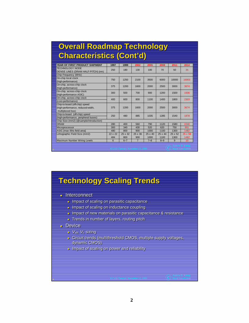
22
3
Andrew B. KahngMajid SarrafzadehICCAD Tutorial: November 11, 1999 C
Overall Roadma p Technolo gyCharacteristics (Cont’d )Overall Roadma p Technolo gyOverall Roadma p Technolo gyCharacteristics (Characteristics (Cont’dCont’d ))
YEAR OF FIRST PRODUCT SHIPMENT 1997 1999 2002 2005 2008 2011 2014TECHNOLOGY NODEDENSE LINES (DRAM HALF-PITCH) (nm)
On-chip local clock (high-performance) On-chip, across-chip clock (high-performance) On-chip, across-chip clock (high-performance ASIC)On-chip, across-chip clock (cost-performance)Chip-to-board (off-chip) speed (high-performance, reduced-width, multiplexed bus) Chip-to-board (off-chip) speed (high-performance, peripheral buses)
DRAM 280 400 560 790 1120 1580 2240Microprocessor 300 340 430 520 620 750 901ASIC [max litho field area] 480 800 900 1000 1100 1300 1482Lithographic Field Size (mm2) 22 x 22 25 x 32 25 x 36 25 x 40 25 x 44 25 x 52 25 x 59
484 800 900 1000 1100 1300 1482Maximum Number Wiring Levels 6 6–7 7 7–8 8–9 9 10
Chip Size (mm2) (@sample/introduction)
2500 3000 3674
250 480 885 1035 1285 1540 1878
375 1200 1600 2000
1200 1500 1936
400 600 800 1100 1400 1800 2303
300 500 700 900
6000 10000 16903
375 1200 1600 2000 2500 3000 3674
750 1250 2100 3500
70 50 35
Chip Frequency (MHz)
250 180 130 100
4
Andrew B. KahngMajid SarrafzadehICCAD Tutorial: November 11, 1999 C
Technolo gy Scalin g TrendsTechnolo gy Scalin g TrendsTechnolo gy Scalin g Trends
z Interconnectz Impact of scaling on parasitic capacitance
z Impact of scaling on inductance coupling
z Impact of new materials on parasitic capacitance & resistance
z Trends in number of layers, routing pitch
z Devicez Vdd, Vt, sizing
z Circuit trends (multithreshold CMOS, multiple supply voltages,dynamic CMOS)
z Impact of scaling on power and reliability

33
5
Andrew B. KahngMajid SarrafzadehICCAD Tutorial: November 11, 1999 C
Technolo gy Scalin g TrendsTechnolo gy Scalin g TrendsTechnolo gy Scalin g Trends
25 x 25 mm chip
Reachability in τcrit = 80 psReachability in τcrit = 80 ps
6
Andrew B. KahngMajid SarrafzadehICCAD Tutorial: November 11, 1999 C
Technolo gy Scalin g TrendsTechnolo gy Scalin g TrendsTechnolo gy Scalin g Trends
z Scaling of x0.7 every three yearsz .25u .18u .13u .10u .07u .05uz 1997 1999 2002 2005 2008 2011z 5LM 6LM 7LM 7LM 8LM 9LM
z Interconnect delay dominates system performancez consumes 70% of clock cycle
z cross coupling capacitance is dominatingz cross capacitance → 100%, ground capacitance → 0%z 90% in .18uz huge signal integrity implications (e.g., guardbands in static
analysis approaches)
44
7
Andrew B. KahngMajid SarrafzadehICCAD Tutorial: November 11, 1999 C
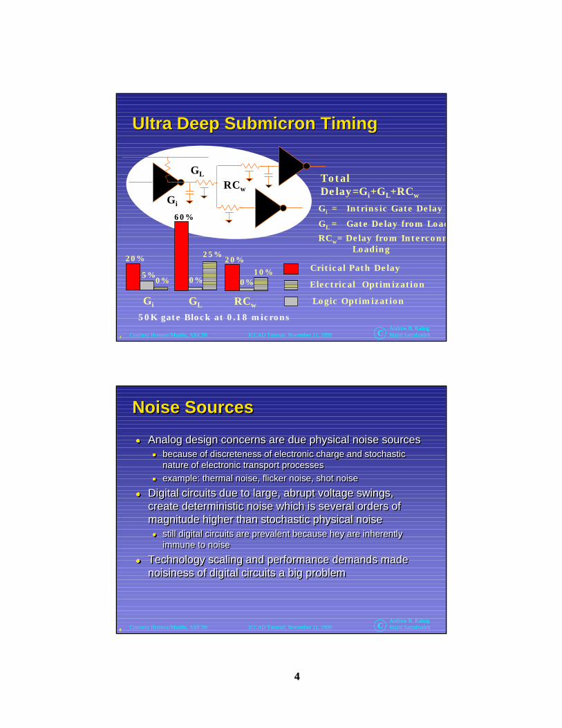
Ultra Dee pUltra Dee p Submicron Submicron Timin g Timin g
Gi
GL
RCw
Gi = Intrinsic Gate Delay
GL = Gate Delay from Load
RCw= Delay from Interconn Loading
TotalDelay=Gi+GL+RCw
Gi GL RCw
20%
60%
20%
5%
25%
10%0% 0%0%
50K gate Block at 0.18 microns
Critical Path Delay
Logic Optimization
Electrical Optimization
Courtesy Hormoz/Muddu, ASIC99
8
Andrew B. KahngMajid SarrafzadehICCAD Tutorial: November 11, 1999 CCourtesy Hormoz/Muddu, ASIC99
Noise SourcesNoise SourcesNoise Sources
z Analog design concerns are due physical noise sourcesz because of discreteness of electronic charge and stochastic
nature of electronic transport processesz example: thermal noise, flicker noise, shot noise
z Digital circuits due to large, abrupt voltage swings,create deterministic noise which is several orders ofmagnitude higher than stochastic physical noisez still digital circuits are prevalent because hey are inherently
immune to noise
z Technology scaling and performance demands madenoisiness of digital circuits a big problem

55
9
Andrew B. KahngMajid SarrafzadehICCAD Tutorial: November 11, 1999 C
0.13
0.18
0.25
0.35
0.5 0
2
4
6
8
10
12
14
16
18
Estimated Number of Nets At-Risk
At-
Ris
k N
ets
(mill
ions
)
Technology (µ)
Risk Factors:Interconnect DelaySignal IntegrityElectromigrationProcess Variations
Courtesy Hormoz/Muddu, ASIC99
Deep-Submicron InterconnectComplexityDeep-Deep-SubmicronSubmicron Interconnect InterconnectComplexityComplexity
10
Andrew B. KahngMajid SarrafzadehICCAD Tutorial: November 11, 1999 CCourtesy Hormoz/Muddu, ASIC99
Scaling of Noise with ProcessScaling of Noise with ProcessScaling of Noise with Process
z Cross coupling noise increases withz process shrinkz frequency of operation
z Propagated noise increases with decrease in noisemarginsz decrease in supply voltagez more extreme P/N ratios for high speed operation
z IR drop noise increases withz complexity of chip sizez frequency of chipz shrinking of metal layers
66
11
Andrew B. KahngMajid SarrafzadehICCAD Tutorial: November 11, 1999 C
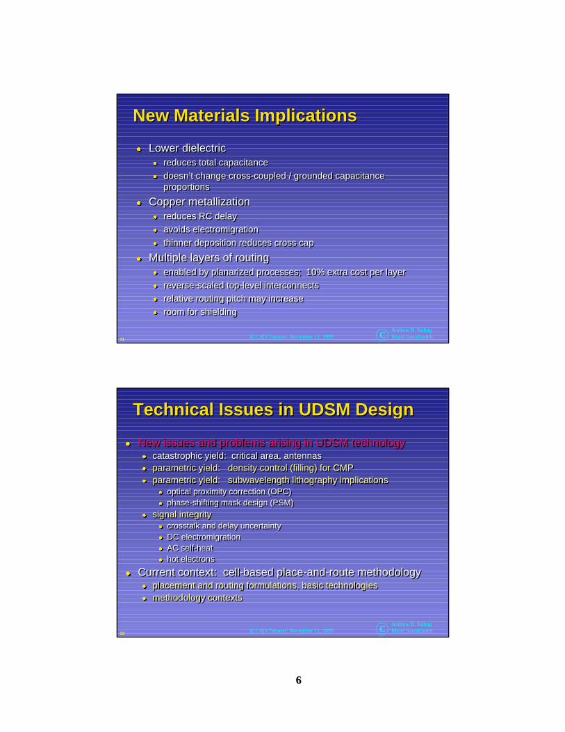
New Materials Im plicationsNew Materials Im plicationsNew Materials Im plications
z Lower dielectricz reduces total capacitancez doesn’t change cross-coupled / grounded capacitance
proportions
z Copper metallizationz reduces RC delayz avoids electromigrationz thinner deposition reduces cross cap
z Multiple layers of routingz enabled by planarized processes; 10% extra cost per layerz reverse-scaled top-level interconnectsz relative routing pitch may increasez room for shielding
12
Andrew B. KahngMajid SarrafzadehICCAD Tutorial: November 11, 1999 C
Technical Issues in UDSM Desi gnTechnical Issues in UDSM Desi gnTechnical Issues in UDSM Desi gn
z New issues and problems arising in UDSM technologyz catastrophic yield: critical area, antennasz parametric yield: density control (filling) for CMPz parametric yield: subwavelength lithography implications
z optical proximity correction (OPC)z phase-shifting mask design (PSM)
z signal integrityz crosstalk and delay uncertaintyz DC electromigrationz AC self-heatz hot electrons
z Current context: cell-based place-and-route methodologyz placement and routing formulations, basic technologiesz methodology contexts

77
13
Andrew B. KahngMajid SarrafzadehICCAD Tutorial: November 11, 1999 C
Technical Issues in UDSM Desi gnTechnical Issues in UDSM Desi gnTechnical Issues in UDSM Desi gn
z Manufacturability (chip can't be built)z antenna rulesz minimum area rules for stacked viasz CMP (chemical mechanical polishing) area fill rulesz layout corrections for optical proximity effects in subwavelength
lithography; associated verification issues
z Signal integrity (failure to meet timing targets)z crosstalk induced errorsz timing dependence on crosstalkz IR drop on power supplies
z Reliability (design failures in the field)z electromigration on power suppliesz hot electron effects on devicesz wire self heat effects on clocks and signals
14
Andrew B. KahngMajid SarrafzadehICCAD Tutorial: November 11, 1999 C
Why Now?Why Now?Why Now?
z These effects have always existed, but become worseat UDSM sizes because of:z finer geometries
z greater wire and via resistancez higher electric fields if supply voltage not scaled
z more metal layersz higher ratio of cross coupling to grounded capacitance
z lower supply voltagesz more current for given power
z lower device thresholdsz smaller noise margins
z Focus on interconnectz susceptible to patterning difficulties
z CMP, optical exposure, resist development/etch, CVD, ...z susceptible to defects
z critical area, critical volume

88
15
Andrew B. KahngMajid SarrafzadehICCAD Tutorial: November 11, 1999 C
Example: Defect-related Yield LossExample: Defect-related Yield LossExample: Defect-related Yield Loss
z High susceptibility to spot defect-related yield loss,particularly in metallization stages of process
z Most common failure mechanisms: shorts or opens dueto extra or missing material between metal tracks
z Design tools fail to realize that values in design manualsare minimum values, not target values
z Spot defect yield loss modelingz extremely well-studied fieldz first-order yield prediction: Poisson yield modelz critical-area model much more successfulz fatal defect types (two types of short circuits, one type of open)
16
Andrew B. KahngMajid SarrafzadehICCAD Tutorial: November 11, 1999 C
Defect-related Yield LossDefect-related Yield LossDefect-related Yield Loss
fatal defect types (two types of short circuits, one type of open)

99
17
Andrew B. KahngMajid SarrafzadehICCAD Tutorial: November 11, 1999 C
Critical Area for Short CircuitsCritical Area for Short CircuitsCritical Area for Short Circuits
Critical Area for Shorts
18
Andrew B. KahngMajid SarrafzadehICCAD Tutorial: November 11, 1999 C
Critical Area for Short CircuitsCritical Area for Short CircuitsCritical Area for Short Circuits
Critical Areafor Shorts

1010
19
Andrew B. KahngMajid SarrafzadehICCAD Tutorial: November 11, 1999 C
Approaches to S pot Defect YieldLossApproaches to S pot Defect YieldApproaches to S pot Defect YieldLossLossz Modify wire placements to minimize critical areaz Router issue
z router understands critical-area analyses, optimizationsz spread, push/shove (gridless, compaction technology)z layer reassignment, via shifting (standard capabilities)z related: via doubling when available, etc.
z Post-processing approaches in PV are awkwardz breaks performance verification in layout (if layout has been
changed by physical verification)z no easy loop back to physical design: convergence problems
z Modify wire placements to minimize critical areaz Router issue
z router understands critical-area analyses, optimizationsz spread, push/shove (gridless, compaction technology)z layer reassignment, via shifting (standard capabilities)z related: via doubling when available, etc.
z Post-processing approaches in PV are awkwardz breaks performance verification in layout (if layout has been
changed by physical verification)z no easy loop back to physical design: convergence problems
20
Andrew B. KahngMajid SarrafzadehICCAD Tutorial: November 11, 1999 C
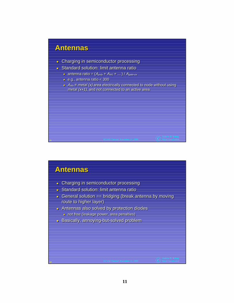
Example: AntennasExample: AntennasExample: Antennas
z Charging in semiconductor processingz many process steps use plasmas, charged particlesz charge collects on conducting poly, metal surfacesz capacitive coupling: large electrical fields over gate oxidesz stresses cause damage, or complete breakdownz induced Vt shifts affect device matching (e.g., in analog)
z Charging in semiconductor processingz many process steps use plasmas, charged particlesz charge collects on conducting poly, metal surfacesz capacitive coupling: large electrical fields over gate oxidesz stresses cause damage, or complete breakdownz induced Vt shifts affect device matching (e.g., in analog)
1111
21
Andrew B. KahngMajid SarrafzadehICCAD Tutorial: November 11, 1999 C
AntennasAntennasAntennas
z Charging in semiconductor processingz Standard solution: limit antenna ratio
z antenna ratio = (Apoly + AM1 + ... ) / Agate-ox
z e.g., antenna ratio < 300
z AMx ≡ metal (x) area electrically connected to node without usingmetal (x+1), and not connected to an active area
z Charging in semiconductor processingz Standard solution: limit antenna ratio
z antenna ratio = (Apoly + AM1 + ... ) / Agate-ox
z e.g., antenna ratio < 300
z AMx ≡ metal (x) area electrically connected to node without usingmetal (x+1), and not connected to an active area
22
Andrew B. KahngMajid SarrafzadehICCAD Tutorial: November 11, 1999 C
AntennasAntennasAntennas
z Charging in semiconductor processingz Standard solution: limit antenna ratioz General solution == bridging (break antenna by moving
route to higher layer)z Antennas also solved by protection diodes
z not free (leakage power, area penalties)
z Basically, annoying-but-solved problem
z Charging in semiconductor processingz Standard solution: limit antenna ratioz General solution == bridging (break antenna by moving
route to higher layer)z Antennas also solved by protection diodes
z not free (leakage power, area penalties)
z Basically, annoying-but-solved problem
1212
23
Andrew B. KahngMajid SarrafzadehICCAD Tutorial: November 11, 1999 C
Silicon Com plexit y and Desi gnComplexit ySilicon Com plexit y and Desi gnSilicon Com plexit y and Desi gnComplexit yComplexit yz Silicon complexity: physical effects cannot be ignored
z fast but weak gates; resistive and cross-coupled interconnectsz subwavelength lithography from 350nm generation onwardz delay, power, signal integrity, manufacturability, reliability all
become first-class objectives along with area
z Design complexity: more functionality andcustomization, in less timez reuse-based design methodologies for SOC
z Interactions increase complexityz need robust, top-down, convergent design methodology
z Silicon complexity: physical effects cannot be ignoredz fast but weak gates; resistive and cross-coupled interconnectsz subwavelength lithography from 350nm generation onwardz delay, power, signal integrity, manufacturability, reliability all
become first-class objectives along with area
z Design complexity: more functionality andcustomization, in less timez reuse-based design methodologies for SOC
z Interactions increase complexityz need robust, top-down, convergent design methodology
24
Andrew B. KahngMajid SarrafzadehICCAD Tutorial: November 11, 1999 C
Guidin g Philoso phy in the Back-EndGuidin g Philoso phy in the Back-EndGuidin g Philoso phy in the Back-End
z Many opportunities to leave $$$ on tablez physical effects of process, migratabilityz design rules more conservative, design waivers upz device-level layout optimizations in cell-based methodologies
z Verification cost increasesz Prevention becomes necessary complement to
checkingz Successive approximation = design convergence
z upstream activities pass intentions, assumptions downstreamz downstream activities must be predictablez models of analysis/verification = objectives for synthesis
z More “custom” bias in automated methodologies

1313
25
Andrew B. KahngMajid SarrafzadehICCAD Tutorial: November 11, 1999 C
Implications of Com plexit yImplications of Com plexit yImplications of Com plexit y
z UDSM: Silicon complexity + Design complexityz convergent design: must abstract what’s beneath
z prevention with respect to analysis/verification checksz many issues to worry about (all are “first-class citizens”z apply methodology (P/G/clock design, circuit tricks, …) whenever possible
z must concede loss of clean abstractions: need unificationsz synthesis and analysis in tight loopz logic and layout : chip implementation planning methodologiesz layout and manufacturing : CMP/OPC/PSM, yield, reliability, SI, statistical
design, …
z must hit function/cost/TAT points that maximize $/waferz reuse-based methodology
z need for differentiating IP → custom -ization
26
Andrew B. KahngMajid SarrafzadehICCAD Tutorial: November 11, 1999 C
Wire Spacin g and La yout Methodolo gyWire Spacin g and La yout Methodolo gyWire Spacin g and La yout Methodolo gy
z Routing tools do not always optimize for spacingz Stand-alone spacing
z layout (GDSII/DEF) -> layout (GDSII/DEF)z Need tight interface to extraction and timing simulationz Future: built-in extraction and timing estimates
z Routing tools do not always optimize for spacingz Stand-alone spacing
z layout (GDSII/DEF) -> layout (GDSII/DEF)z Need tight interface to extraction and timing simulationz Future: built-in extraction and timing estimates
Courtesy M. Berkens, DAC99

1414
27
Andrew B. KahngMajid SarrafzadehICCAD Tutorial: November 11, 1999 C
Data Aspects of Post La yout OptimizationData Aspects of Post La yout OptimizationData Aspects of Post La yout Optimization
z Jogging increases amount of data significantlyz Massive data needs striping
z minor loss of optimality for large stripesz need work across hierarchyz fix boundary location, “look” beyond cut-linez need propagate net information
z Must support multi-processing for reasonable TAT
z Jogging increases amount of data significantlyz Massive data needs striping
z minor loss of optimality for large stripesz need work across hierarchyz fix boundary location, “look” beyond cut-linez need propagate net information
z Must support multi-processing for reasonable TAT
Courtesy M. Berkens, DAC99
28
Andrew B. KahngMajid SarrafzadehICCAD Tutorial: November 11, 1999 C
Wire Spacin g and Shieldin gWire Spacin g and Shieldin gWire Spacin g and Shieldin g
z Pre routing specificationz convenient, handled by routerz robust but conservativez may consume big area
z Post routing specificationz area efficient-shield only where needed & have spacez ease task of routerz sufficient shielding is not guaranteed
z Pre routing specificationz convenient, handled by routerz robust but conservativez may consume big area
z Post routing specificationz area efficient-shield only where needed & have spacez ease task of routerz sufficient shielding is not guaranteed
Courtesy M. Berkens, DAC99
1515
29
Andrew B. KahngMajid SarrafzadehICCAD Tutorial: November 11, 1999 C
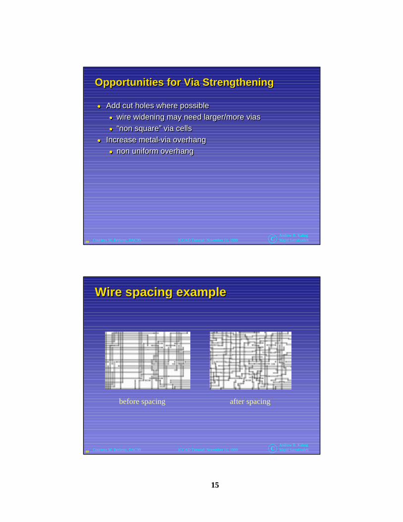
Opportunities for Via Stren gthenin gOpportunities for Via Stren gthenin gOpportunities for Via Stren gthenin g
z Add cut holes where possiblez wire widening may need larger/more viasz “non square” via cells
z Increase metal-via overhangz non uniform overhang
z Add cut holes where possiblez wire widening may need larger/more viasz “non square” via cells
z Increase metal-via overhangz non uniform overhang
Courtesy M. Berkens, DAC99
30
Andrew B. KahngMajid SarrafzadehICCAD Tutorial: November 11, 1999 C
Wire s pacin g exampleWire s pacin g exampleWire s pacin g example
before spacing after spacing
Courtesy M. Berkens, DAC99

1616
31
Andrew B. KahngMajid SarrafzadehICCAD Tutorial: November 11, 1999 C
Performance Optimization Methodolo gyDesign TradeoffsPerformance Optimization Methodolo gyPerformance Optimization Methodolo gyDesign TradeoffsDesign Tradeoffs
z Speed / Power / Areaz Must compromise and choose between often competing
criteriaz For given criteria (constraints) on some variables, make
best choice for free variables (min cost) => Need to beon boundary of feasible region
z Speed / Power / Areaz Must compromise and choose between often competing
criteriaz For given criteria (constraints) on some variables, make
best choice for free variables (min cost) => Need to beon boundary of feasible region
Courtesy Bamji, DAC99
32
Andrew B. KahngMajid SarrafzadehICCAD Tutorial: November 11, 1999 C
OptimizationMethodsOptimizationOptimizationMethodsMethods
z Many different kinds of delay/area optimization arepossible
z Many optimizations are somewhat independentz use several different optimizations. Apply whichever ones are
applicable
z Many different kinds of delay/area optimization arepossible
z Many optimizations are somewhat independentz use several different optimizations. Apply whichever ones are
applicable
Reorganize Logic
Buffer
Size
Space
Retime
Courtesy Bamji, DAC99
1717
33
Andrew B. KahngMajid SarrafzadehICCAD Tutorial: November 11, 1999 C
Optimization at La yout LevelOptimization at La yout LevelOptimization at La yout Level
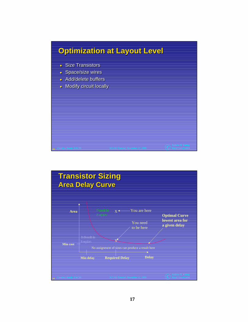
z Size Transistorsz Space/size wiresz Add/delete buffersz Modify circuit locally
z Size Transistorsz Space/size wiresz Add/delete buffersz Modify circuit locally
Courtesy Bamji, DAC99
34
Andrew B. KahngMajid SarrafzadehICCAD Tutorial: November 11, 1999 C
Transistor Sizin gArea Dela y CurveTransistor Sizin gTransistor Sizin gArea Dela y CurveArea Dela y Curve
Min delay
Min cost
Required Delay Delay
Area
Infeasi bleRegion
Feasi bleRegion
No assignment of sizes can produce a result here
Optimal Curvelowest area fora given delay
You are hereX
You needto be here
X
Courtesy Bamji, DAC99

1818
35
Andrew B. KahngMajid SarrafzadehICCAD Tutorial: November 11, 1999 C
Transistor sizin gWhat will it bu y me?Transistor sizin gTransistor sizin gWhat will it bu y me?What will it bu y me?z Scenario: Lots of capacitance in wires
z will it buy me speed: Yesz will is save me power: “Yes” (qualified)
z Scenario: Lots of capacitance in wiresz will it buy me speed: Yesz will is save me power: “Yes” (qualified)
Delay
Area Architecture isan overkill forthis application
Architecture cannotsatisfy application(increase parallelism)
Delay can be improvedat almost no cost
Delay cannotbe improvedat any cost
Architecture andapplication arewell matched
Courtesy Bamji, DAC99
36
Andrew B. KahngMajid SarrafzadehICCAD Tutorial: November 11, 1999 C
Transistor Sizin gConvexit y + Dual GoalsTransistor Sizin gTransistor Sizin gConvexit y + Dual GoalsConvexit y + Dual Goals
Circuits of constant cost W1 +W2 = Cte
W1(size of Xtr1)
W2(size of Xtr2)
5ns 10ns
Circuits of constant delay:15nsFaster circuits inside this curve
Note: Actually circuit delay is Posynomial ~ Convex
Optimalpoint for10ns
Courtesy Bamji, DAC99
1919
37
Andrew B. KahngMajid SarrafzadehICCAD Tutorial: November 11, 1999 C
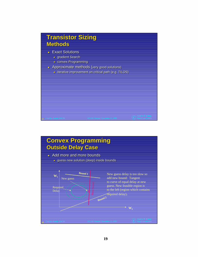
Transistor Sizin gMethodsTransistor Sizin gTransistor Sizin gMethodsMethodsz Exact Solutions
z gradient Searchz convex Programming
z Approximate methods (very good solutions)
z iterative improvement on critical path (e.g. TILOS)
z Exact Solutionsz gradient Searchz convex Programming
z Approximate methods (very good solutions)
z iterative improvement on critical path (e.g. TILOS)
Courtesy Bamji, DAC99
38
Andrew B. KahngMajid SarrafzadehICCAD Tutorial: November 11, 1999 C
Convex Pro grammin gOutside Dela y CaseConvex Pro grammin gConvex Pro grammin gOutside Dela y CaseOutside Dela y Casez Add more and more bounds
z guess new solution (deep) inside bounds
z Add more and more boundsz guess new solution (deep) inside bounds
W1
W2
Bound 1
Bound 2
New guess
X
RequiredDelay
New
bou
nd
New guess delay is too slow soadd new bound: Tangentto curve of equal delay at newguess. New feasible region isto the left (region which contains
required delay).
Courtesy Bamji, DAC99

2020
39
Andrew B. KahngMajid SarrafzadehICCAD Tutorial: November 11, 1999 C
Convex Pro grammin gInside Dela y CaseConvex Pro grammin gConvex Pro grammin gInside Dela y CaseInside Dela y Casez New guess delay is adequate but try and improve costz New guess delay is adequate but try and improve cost
Add a bound to forcesearch into regionof lower cost. New boundis constant cost curvepassing through newguess. New feasibleregion is below newbound.
W1
W2
Bound 1
Bound 2
New guess
RequiredDelay
Bou
nd 3
X New boundConstant cost
Courtesy Bamji, DAC99
40
Andrew B. KahngMajid SarrafzadehICCAD Tutorial: November 11, 1999 C
Transistor Sizin gApproximate SolutionsTransistor Sizin gTransistor Sizin gApproximate SolutionsApproximate Solutions
W1
W2
Move minimally in thisdirection D2 to reduce cost
Move maximally in thisdirection D1 to improve delay
Constant
cost
Constant Delay
Circuit delay affectedonly by delay ofcritical path. Upsize bysmall amounttransistors on crit pathwith biggest D1/D2 =improvement/cost.Repeat until timing met
Courtesy Bamji, DAC99

2121
41
Andrew B. KahngMajid SarrafzadehICCAD Tutorial: November 11, 1999 C
Transistor Sizin gTILOS methodTransistor Sizin gTransistor Sizin gTILOS methodTILOS method
z Increase Xtr on critical path with largest per uniteffective speedup: T
z Increase Xtr on critical path with largest per uniteffective speedup: T
3
4
5
Critical Path
T
Effective speedupper unit area
δ1= speedup of Tδ2 = slowdown of T
Effective speedup ofT = δ1 - δ2 = 5
Courtesy Bamji, DAC99
42
Andrew B. KahngMajid SarrafzadehICCAD Tutorial: November 11, 1999 C
Short Circuit Power OptimizationShort Circuit Power OptimizationShort Circuit Power Optimization
z Critical path methods miss short circuit power
z Increase Islow until capacitive power increase for driving Islow is morethan decrease in S.C. powerz sweep circuit from outputs to inputs
z Critical path methods miss short circuit power
z Increase Islow until capacitive power increase for driving Islow is morethan decrease in S.C. powerz sweep circuit from outputs to inputs
Short circuit power burnedin all of these gates due toslow input rise time. Gates noton critical pathSlow node
Critical path
Islow
Courtesy Bamji, DAC99

2222
43
Andrew B. KahngMajid SarrafzadehICCAD Tutorial: November 11, 1999 C
TILOS Optimization Tra jector yTILOS Optimization Tra jector yTILOS Optimization Tra jector y
Delay
Power
Infeasi bleRegion
Starting Point.
X
XX
X
ReduceS.C.
downsize
fix timing
Red
uce
S. C
ircui
t.
Feasi bleRegion
Required delay
Note:Min Size != Min Power
Courtesy Bamji, DAC99
44
Andrew B. KahngMajid SarrafzadehICCAD Tutorial: November 11, 1999 C
Buffer InsertionArea dela y tradeoffsBuffer InsertionBuffer InsertionArea dela y tradeoffsArea dela y tradeoffs
z Optimal curve is envelope of curvesz jump to buffered curve during timing optimization
z Optimal curve is envelope of curvesz jump to buffered curve during timing optimization
Delay
Area
With buffer
Without buffer
OptimizationTrajectory
Add buffer atthis point
Feasi ble RegionIs the Union of bothfeasible regions
Area of MinSize buffer
Courtesy Bamji, DAC99
2323
45
Andrew B. KahngMajid SarrafzadehICCAD Tutorial: November 11, 1999 C
Local Re-s ynthesisLocal Re-s ynthesisLocal Re-s ynthesis
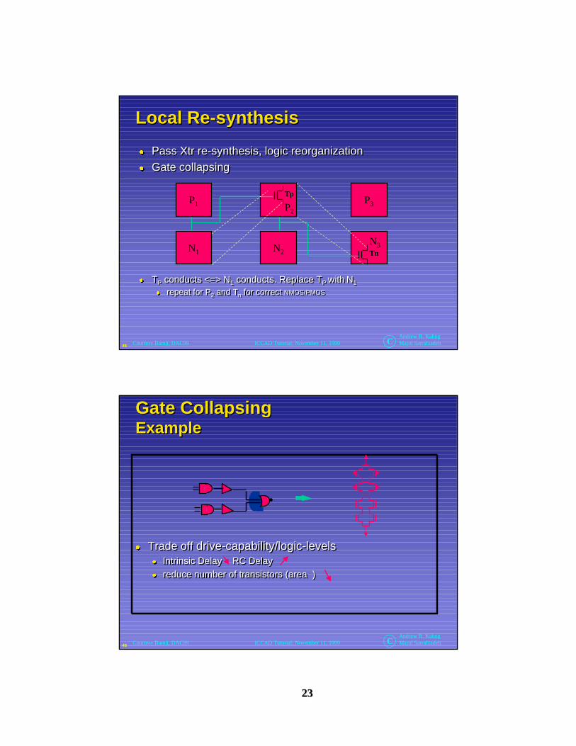
z Pass Xtr re-synthesis, logic reorganizationz Gate collapsing
z TP conducts <=> N1 conducts. Replace TP with N1
z repeat for P2 and Tn for correct NMOS/PMOS
z Pass Xtr re-synthesis, logic reorganizationz Gate collapsing
z TP conducts <=> N1 conducts. Replace TP with N1
z repeat for P2 and Tn for correct NMOS/PMOS
N2
P3P1
N1
P2
N3
Tp
Tn
Courtesy Bamji, DAC99
46
Andrew B. KahngMajid SarrafzadehICCAD Tutorial: November 11, 1999 C
Gate Colla psin gExampleGate Colla psin gGate Colla psin gExampleExample
z Trade off drive-capability/logic-levelsz Intrinsic Delay RC Delayz reduce number of transistors (area )
z Trade off drive-capability/logic-levelsz Intrinsic Delay RC Delayz reduce number of transistors (area )
Courtesy Bamji, DAC99

2424
47
Andrew B. KahngMajid SarrafzadehICCAD Tutorial: November 11, 1999 C
Performance Optimization Methodolo gyPerformance Optimization Methodolo gyPerformance Optimization Methodolo gyz Design Optimization
z global restructuring optimization -- logic optimization on layoutusing actual RC, noise peak values etc.
z localized optimization -- with no structural changes and leastlayout impact
z repeater/buffer insertion for global wires
z Physical optimizationz high fanout net synthesis (eg. for clock nets); buffer trees to meet
delay/skew and fanout requirementsz automatically determine network topology (# levels, #buffers, and
type of buffers)z wire sizing, spacing, shielding etc.
z Fixing timing violations automaticallyz fix setup/hold time violationsz fix maximum slew and fanout violations
z Design Optimizationz global restructuring optimization -- logic optimization on layout
using actual RC, noise peak values etc.z localized optimization -- with no structural changes and least
layout impactz repeater/buffer insertion for global wires
z Physical optimizationz high fanout net synthesis (eg. for clock nets); buffer trees to meet
delay/skew and fanout requirementsz automatically determine network topology (# levels, #buffers, and
type of buffers)z wire sizing, spacing, shielding etc.
z Fixing timing violations automaticallyz fix setup/hold time violationsz fix maximum slew and fanout violations
Courtesy Hormoz/Muddu, ASIC99
48
Andrew B. KahngMajid SarrafzadehICCAD Tutorial: November 11, 1999 C
Performance Optimization Tool FlowPerformance Optimization Tool FlowPerformance Optimization Tool FlowArchitectural/ Behavioral Design
Extraction
Timing Analysis
Signal Integrity Analysis
RTL Design
Optimization
Floor Planning
Placement
Logic Synthesis
Global Routing Detailed Routing
Electrical Analysis/Estimation
EM Analysis
Power Analysis
ClockAnalysis
Courtesy Hormoz/Muddu, ASIC99

2525
49
Andrew B. KahngMajid SarrafzadehICCAD Tutorial: November 11, 1999 C
Custom Methodolo gy in ASIC(?) / COTCustom Methodolo gy in ASIC(?) / COTCustom Methodolo gy in ASIC(?) / COT
z How much is on the table w.r.t. performance?z 4x speed, 1/3x area, 1/10x power (Alpha vs. Strongarm vs. “ASIC”)z layout methodology spans RTL syn, auto P&R, tiling/generation,
manual
z library methodology spans gate array, std cell, rich std cell, liquid lib,…
z Traditional view of cell-based ASICz Advantages: high productivity, TTM, portability (soft IP, gates)z Disadvantages: slower, more power, more area, slow production
of std cell library
z Traditional view of Customz Advantages: faster, less power, less area, more circuit stylesz Disadvantages: low productivity, longer TTM, limited reuse
50
Andrew B. KahngMajid SarrafzadehICCAD Tutorial: November 11, 1999 C
Custom Methodolo gy in ASIC(?) / COTCustom Methodolo gy in ASIC(?) / COTCustom Methodolo gy in ASIC(?) / COT
z With sub-wavelength lithography:z how much more guardbanding will standard cells need?z composability is difficult to guarantee at edges of PSM layouts,
when PSM layouts are routed, when hard IPs are made withdifferent density targets, etc.
z context-independent composability is the foundation of cell-based methodology!
z With variant process flavors:z hard layouts (including cells) will be more difficult to reuse
z → Relative cost of custom decreasesz On the other hand, productivity is always an issue...

2626
51
Andrew B. KahngMajid SarrafzadehICCAD Tutorial: November 11, 1999 C
Custom Methodolo gy in ASIC(?) / COTCustom Methodolo gy in ASIC(?) / COTCustom Methodolo gy in ASIC(?) / COT
z Architecturez heavy pipeliningz fewer logic levels between latches
z Dynamic logicz used on all critical paths
z Hand-crafted circuit topologies, sizing and layoutz good attention to design reduces guardbands
The last seems to be the lowest-han ging fruit for ASIC
z Architecturez heavy pipeliningz fewer logic levels between latches
z Dynamic logicz used on all critical paths
z Hand-crafted circuit topologies, sizing and layoutz good attention to design reduces guardbands
The last seems to be the lowest-han ging fruit for ASIC
52
Andrew B. KahngMajid SarrafzadehICCAD Tutorial: November 11, 1999 C
Custom Methodolo gy in ASIC(?) / COTCustom Methodolo gy in ASIC(?) / COTCustom Methodolo gy in ASIC(?) / COTz ASIC market forces (IP differentiation) will define needs
for xtor-level analyses and synthesesz Flexible-hierarchical top-down methodology
z basic strategy: iteratively re-optimize chunks of the design asdefined by the layout, i.e., cut out a piece of physical hierarchy,reoptimize it (“peephole optimization”)z for timing/power/area (e.g., for mismatched input arrival times,
slews)z for auto-layout (e.g., pin access and cell porosity for router)z for manufacturability (density control, critical area, phase-
assignability)z DOF’s: diffusion sharing, sizing, new mapping / circuit topology
sol’sz chunk size: as large as possible (tradeoff between near-optimality,
CPU time)
z antecedents: IBM C5M, Motorola CELLERITY, DEC CLEOz “infinite library”recovers performance, density that a 300-cell
library and classic cell-based flow leave on the table
z ASIC market forces (IP differentiation) will define needsfor xtor-level analyses and syntheses
z Flexible-hierarchical top-down methodologyz basic strategy: iteratively re-optimize chunks of the design as
defined by the layout, i.e., cut out a piece of physical hierarchy,reoptimize it (“peephole optimization”)z for timing/power/area (e.g., for mismatched input arrival times,
slews)z for auto-layout (e.g., pin access and cell porosity for router)z for manufacturability (density control, critical area, phase-
assignability)z DOF’s: diffusion sharing, sizing, new mapping / circuit topology
sol’sz chunk size: as large as possible (tradeoff between near-optimality,
CPU time)
z antecedents: IBM C5M, Motorola CELLERITY, DEC CLEOz “infinite library”recovers performance, density that a 300-cell
library and classic cell-based flow leave on the table

2727
53
Andrew B. KahngMajid SarrafzadehICCAD Tutorial: November 11, 1999 C
Custom Methodolo gy in ASIC(?) / COTCustom Methodolo gy in ASIC(?) / COTCustom Methodolo gy in ASIC(?) / COTz Supporting belief: characterization and verification are
increasingly a non-issuez CPUs get faster; size of layout chunks (O(100-1000) xtors) stay
samez natural instance complexity limits due to hierarchy, layers of
interest
z Compactor-based migration tools are an ingredient ?z migration perspective can infer too many constraints that aren’t
there (consequence of compaction mindset)z little clue about integrated performance analyses
z Tuners are an ingredient ? (size, dual-Vt, multi-supply)z limit DOFs (e.g., repeater insertion and clustering, inverter optsz cannot handle modern design rules, all-angle geometriesz not intended to do high-quality layout synthesis
z Layout synthesis is an ingredient ?z requires optimizations based on detailed analyses (routability,
signal integrity, manufacturability), transparent links tocharacterization and verification
z Supporting belief: characterization and verification areincreasingly a non-issue
z CPUs get faster; size of layout chunks (O(100-1000) xtors) staysame
z natural instance complexity limits due to hierarchy, layers ofinterest
z Compactor-based migration tools are an ingredient ?z migration perspective can infer too many constraints that aren’t
there (consequence of compaction mindset)z little clue about integrated performance analyses
z Tuners are an ingredient ? (size, dual-Vt, multi-supply)z limit DOFs (e.g., repeater insertion and clustering, inverter optsz cannot handle modern design rules, all-angle geometriesz not intended to do high-quality layout synthesis
z Layout synthesis is an ingredient ?z requires optimizations based on detailed analyses (routability,
signal integrity, manufacturability), transparent links tocharacterization and verification
54
Andrew B. KahngMajid SarrafzadehICCAD Tutorial: November 11, 1999 C
Custom Methodolo gy in ASIC(?) / COTCustom Methodolo gy in ASIC(?) / COTCustom Methodolo gy in ASIC(?) / COT
z “Layout or re-layout on the fly” is an element ofperformance- and cost-driven ASIC methodology goingforward
z “Polygon layout as a DOF in circuit optimization” is avery small step from “polygon layout as a DOF inprocess migration”z designers are already reconciled to the latter
z “Layout or re-layout on the fly” is an element ofperformance- and cost-driven ASIC methodology goingforward
z “Polygon layout as a DOF in circuit optimization” is avery small step from “polygon layout as a DOF inprocess migration”z designers are already reconciled to the latter

2828
55
Andrew B. KahngMajid SarrafzadehICCAD Tutorial: November 11, 1999 C
Cell-Based P&R: Classic ContextCell-Based P&R: Classic ContextCell-Based P&R: Classic Context
z Architecture designz golden microarchitecture design, behavioral model, RT-level structural
HDL passed to chip planningz cycle time and cycle-accurate timing boundaries established
z hierarchy correspondences (structural-functional, logical (schematic)and physical) well-established
z Chip planningz hierarchical floorplan, mixed hard-soft block placementz block context-sensitivity: no-fly, layer usage, other routing constraints
z route planning of all global nets (control/data signals, clock, P/G)z induces pin assignments/orderings, hard (partial) pre-routes, etc.
z Individual block design -- various P&R methodologiesz Chip assembly -- possibly implicit in above stepsz What follows: qualitative review of key goals, purposes
56
Andrew B. KahngMajid SarrafzadehICCAD Tutorial: November 11, 1999 C
Placement DirectionsPlacement DirectionsPlacement Directions
z Global placementz engines (analytic, top-down partitioning based, (iterative annealing
based) remain the same; all support “anytime” convergent solutionz becomes more hierarchical
z block placement, latch placement before “cell placement”z support placement of partially/probabilistically specified design
z Detailed placementz LEQ/EEQ substitutionz shifting, spacing and alignment for routabilityz ECOs for timing, signal integrity, reliabilityz closely tied to performance analysis backplane (STA/PV)z support incremental “construct by correction” use model

2929
57
Andrew B. KahngMajid SarrafzadehICCAD Tutorial: November 11, 1999 C
Out-of-Box Uses of Routin g ResultsOut-of-Box Uses of Routin g ResultsOut-of-Box Uses of Routin g Results
z Modify floorplanz floorplan compaction, pin assignments derived from top-level route
planning
z Determine synthesis constraintsz budgets for intra-block delay, block input/output boundary conditions
z Modify netlistz driver sizing, repeater insertion, buffer clustering
z Placement directives for block layoutz over-block route planning affects utilization factors within blocks
z Performance-driven routing directivesz wire tapering/spacing/shielding choices, assumed layer assignments,
etc.
58
Andrew B. KahngMajid SarrafzadehICCAD Tutorial: November 11, 1999 C
Function of a UDSM RouterFunction of a UDSMFunction of a UDSM Router Router
z Ultimately responsible for meeting specs/assumptionsz slew, noise, delay, critical-area, antenna ratio, PSM-amenable …
z Checks performability throughout top-down physical impl.z actively understands, invokes analysis engines and macromodels
z Many functionsz circuit-level IP generation: clock, power, test, package substrate
routingz pin assignment and track ordering enginesz monolithic topology optimization enginesz owns key DOFs: small re-mapping, incremental placement,
device-level layout resynthesisz is hierarchical, scalable, incremental, controllable, well-
characterized (well-modeled), detunable (e.g., coarse/quickrouting), ...
3030
59
Andrew B. KahngMajid SarrafzadehICCAD Tutorial: November 11, 1999 C
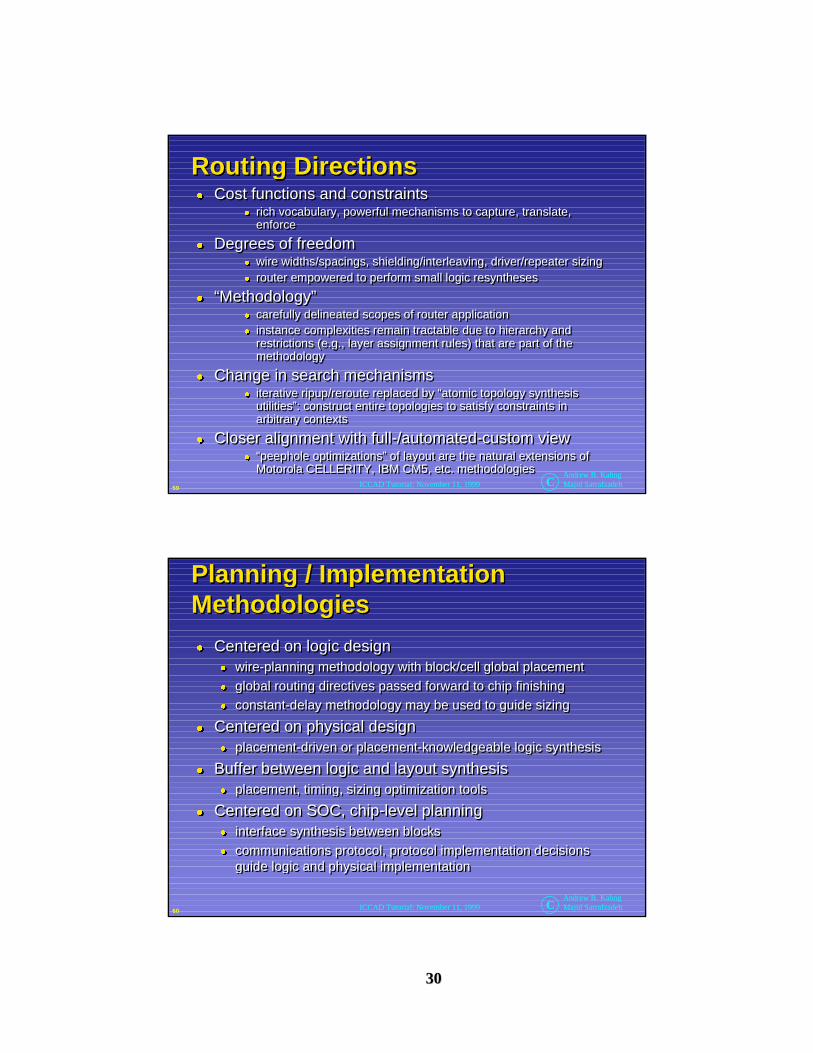
Routin g DirectionsRoutin g DirectionsRoutin g Directionsz Cost functions and constraints
z rich vocabulary, powerful mechanisms to capture, translate,enforce
z Degrees of freedomz wire widths/spacings, shielding/interleaving, driver/repeater sizingz router empowered to perform small logic resyntheses
z “Methodology”z carefully delineated scopes of router applicationz instance complexities remain tractable due to hierarchy and
restrictions (e.g., layer assignment rules) that are part of themethodology
z Change in search mechanismsz iterative ripup/reroute replaced by “atomic topology synthesis
utilities”: construct entire topologies to satisfy constraints inarbitrary contexts
z Closer alignment with full-/automated-custom viewz “peephole optimizations” of layout are the natural extensions of
Motorola CELLERITY, IBM CM5, etc. methodologies
z Cost functions and constraintsz rich vocabulary, powerful mechanisms to capture, translate,
enforce
z Degrees of freedomz wire widths/spacings, shielding/interleaving, driver/repeater sizingz router empowered to perform small logic resyntheses
z “Methodology”z carefully delineated scopes of router applicationz instance complexities remain tractable due to hierarchy and
restrictions (e.g., layer assignment rules) that are part of themethodology
z Change in search mechanismsz iterative ripup/reroute replaced by “atomic topology synthesis
utilities”: construct entire topologies to satisfy constraints inarbitrary contexts
z Closer alignment with full-/automated-custom viewz “peephole optimizations” of layout are the natural extensions of
Motorola CELLERITY, IBM CM5, etc. methodologies
60
Andrew B. KahngMajid SarrafzadehICCAD Tutorial: November 11, 1999 C
Plannin g / ImplementationMethodolo giesPlannin g / ImplementationPlannin g / ImplementationMethodolo giesMethodolo gies
z Centered on logic designz wire-planning methodology with block/cell global placementz global routing directives passed forward to chip finishingz constant-delay methodology may be used to guide sizing
z Centered on physical designz placement-driven or placement-knowledgeable logic synthesis
z Buffer between logic and layout synthesisz placement, timing, sizing optimization tools
z Centered on SOC, chip-level planningz interface synthesis between blocksz communications protocol, protocol implementation decisions
guide logic and physical implementation


