www.iap.uni-jena.de
Metrology and Sensing
Lecture 3: Sensors
2017-11-02
Herbert Gross
Winter term 2017

2
Preliminary Schedule
No Date Subject Detailed Content
1 19.10. Introduction Introduction, optical measurements, shape measurements, errors,
definition of the meter, sampling theorem
2 26.10. Wave optics Basics, polarization, wave aberrations, PSF, OTF
3 02.11. Sensors Introduction, basic properties, CCDs, filtering, noise
4 09.11. Fringe projection Moire principle, illumination coding, fringe projection, deflectometry
5 16.11. Interferometry I Introduction, interference, types of interferometers, miscellaneous
6 23.11. Interferometry II Examples, interferogram interpretation, fringe evaluation methods
7 30.11. Wavefront sensors Hartmann-Shack WFS, Hartmann method, miscellaneous methods
8 07.12. Geometrical methods Tactile measurement, photogrammetry, triangulation, time of flight,
Scheimpflug setup
9 14.12. Speckle methods Spatial and temporal coherence, speckle, properties, speckle metrology
10 21.12. Holography Introduction, holographic interferometry, applications, miscellaneous
11 11.01. Measurement of basic
system properties Bssic properties, knife edge, slit scan, MTF measurement
12 18.01. Phase retrieval Introduction, algorithms, practical aspects, accuracy
13 25.01. Metrology of aspheres
and freeforms Aspheres, null lens tests, CGH method, freeforms, metrology of freeforms
14 01.02. OCT Principle of OCT, tissue optics, Fourier domain OCT, miscellaneous
15 08.02. Confocal sensors Principle, resolution and PSF, microscopy, chromatical confocal method

3
Content
Introduction
Basic properties
CCD
Filtering
Noise

Signal chain
Optical signal detection
T : transfer function
B : signal conversion
N : noise
Signal Chain
),(),(),(),(),( yxNyxCombyxTyxBKyxS D
record of
image pixels
sensorelectronic
systemcomputer
digital data
processing
image
processingdisplay
reproduction
of image pixels
signal detection signal processing reproduction
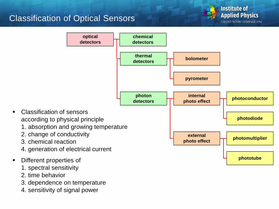
Classification of sensors
according to physical principle
1. absorption and growing temperature
2. change of conductivity
3. chemical reaction
4. generation of electrical current
Different properties of
1. spectral sensitivity
2. time behavior
3. dependence on temperature
4. sensitivity of signal power
Classification of Optical Sensors
chemical
detectors
bolometer
pyrometer
internal
photo effectphotoconductor
external
photo effect
photodiode
photomultiplier
phototube
optical
detectors
thermal
detectors
photon
detectors

Recording of a signal
Dependencies: 1. space coordinate and angle 2. time 3. wavelength
Signal Recording
radiation field
image B(x,y,t,)
image detection
sensor system
sensistivity
discretization
noisesignal
S(x,y,t,)
signal
coding
quantization
noisecoded signal
Se(x,y,t,)
signal
processing
filtering
noise
processingdigital image
I(x,y,t,)
display
discretization
noise
OTF
radiation field
object O(x,y,t,)
optical system
correction
OTF
disturbances
information

2D sensor: Discrete pixel of finite size
Dead zones between pixels: finite effective area of signal collection
Discretizaion and Pixelation
2
pixelD
p
geometric
sensor area
row
columnpixel
pixel
size
Dpixelactive pixel
area
pixel size
p
size of
the grid
element
Dpixel
dead area
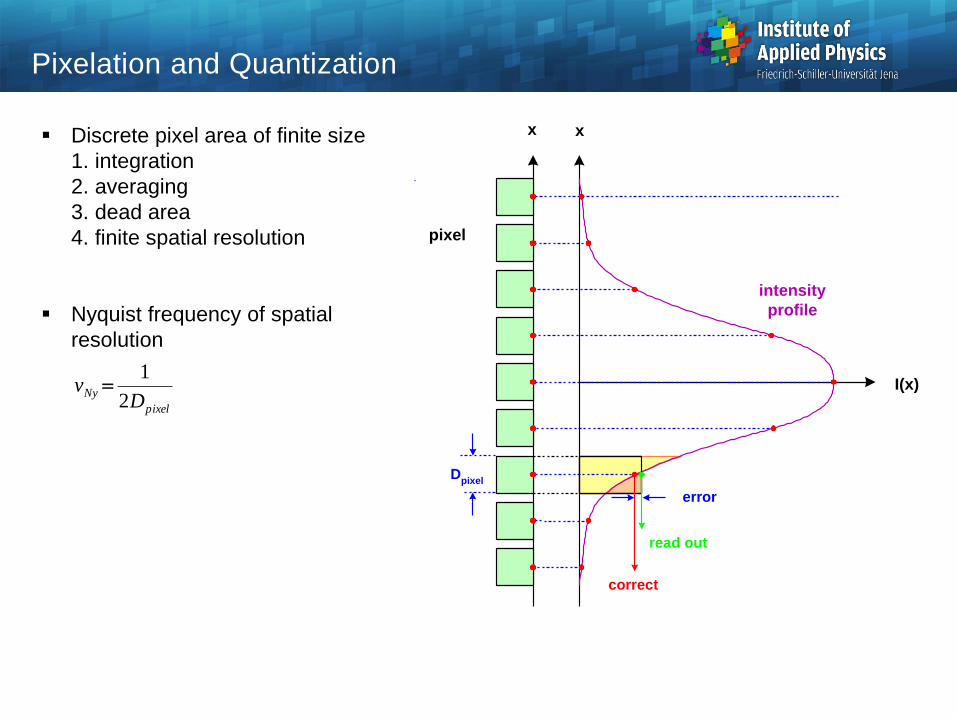
Discrete pixel area of finite size 1. integration 2. averaging 3. dead area 4. finite spatial resolution
Nyquist frequency of spatial resolution
Pixelation and Quantization
pixel
NyD
v2
1
x
I(x)
error
read out
correct
pixel
intensity
profile
x
Dpixel
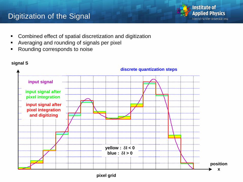
Combined effect of spatial discretization and digitization
Averaging and rounding of signals per pixel
Rounding corresponds to noise
Digitization of the Signal
signal S
position
x
discrete quantization steps
pixel grid
input signal
input signal after
pixel integration
input signal after
pixel integration
and digitizing
yellow : I < 0
blue : I > 0

Acceptance angle of optical sensor
Sensitivity of the response on the incidence angle
Empirical description:
generalized cos-law
Largest sensitivity for normal incidence
Sensitivity on Direction
mss cos)( 0
m = 0.5
m = 1
m = 2
m = 4
m =8
m = 14
m = 50
30
60
90-90
-60
-30
0

Wavelength sensitive detection with CCD:
- array structures with different spectral sensitivity
- reduced spatial resolution
Alternatives:
- depth resolved layers
- time multiplexing
- spatial separation by filter
Detection of Color
Bayer Color Filter Array
R
G B
G
G
G
G G
G
G
G
G
G
GR
R
R
RR
B B
B B
B
Sony Color Filter Array
G B
G
G
G R
R
B
G B
G
G
G R
R
B
G B
G
G
G R
R
B
Hitachi Color Filter Array
G
G
C
G
G
W
C W
G
G
C
G
G
W
C W
G
G
C
G
G
W
C W

Spectral properties:
sensitive in VIS and NIR
Degrading effects:
1. diffusion of electrons, blooming
2. dead zones, reduced efficiency
3. noise of reading process
4. dark current
5. quantum efficiency, 80%
6. time delay, hysteresis
CCD Sensors
200 400 600 800 1000 1200
0
0.2
0.4
0.6
0.8
1
visible
range

Spectral Sensitivity of a CCD Sensor
Typical sensor of a SLR photo camera:
Canon 5D
RGB sensitivity curves at daylight
Ref: D. Gängler
sensitivity
wavelength
in [nm]
thin lines:
ISO norm
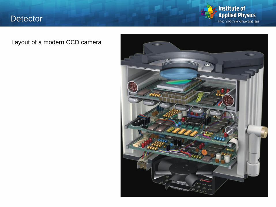
Detector
Layout of a modern CCD camera

The spot position is more accurate, if its size is larger than the pixel width
The signal is changed in many pixels, this is more accurate
Spot inside one pixel: exact position cannot be distinguished
Resolution and Spot size
signal S
x
x1
Pixel
signal S
x
x2
pixel
small spot :
equal signal
x = x2 - x
1 not measurable
Dspot
Dpixel
signal S
x
x1
signal S
x
x2
large spot :
different signal
x = x2 - x
1 is measurable
Dspot
signal changes

Optical system with fixed camera position
Change of object distance:
- s too small: broadening of spot
- focussed: optimal signal transfer
- s too large: broadening of spot, saturation for extreme distances
Gain of Information
a
s's
focussed
receiver
planes too large s too small
spot Dspot

Gain of information as a function of the object distance
Gain of Information
10-2
10-1
100
information
density
ideal
NA large
ideal
NA small
stopped
down
10-2 100 10+2 10+4 10+6object
distance
s in a.u.

Quantization of signal in intervals of finite size I
Typical powers of 2 are used
8 bit corresponds to 256 value of the signal
Rounding of real numbers is equivalent to signal noise
Noise equivalent power
Representation of discretized black-white image as gray levels
Discretization of the Signal
I
IM B
max2
12
2
,
IkP quantnoise
dBBN
S6
grey tone division
0 25612864 192
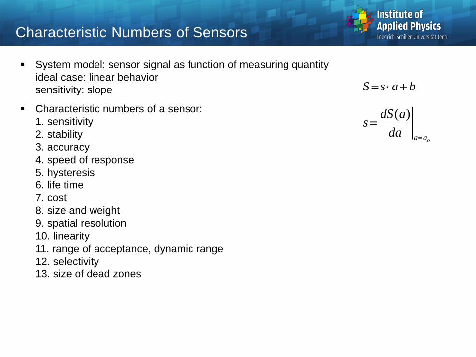
System model: sensor signal as function of measuring quantity
ideal case: linear behavior
sensitivity: slope
Characteristic numbers of a sensor:
1. sensitivity
2. stability
3. accuracy
4. speed of response
5. hysteresis
6. life time
7. cost
8. size and weight
9. spatial resolution
10. linearity
11. range of acceptance, dynamic range
12. selectivity
13. size of dead zones
Characteristic Numbers of Sensors
basS
oaada
adSs
)(

Accuracy of a sensor:
error of signal for a given input
to be distinguished:
1. calibration
2. hysteresis
3. reproduction
4. sample scatter
Accuracy
S
a
range of acceptance
specified
precision
intervalideal linear
transfer
functionreal transfer
function
error interval
error a
error
S
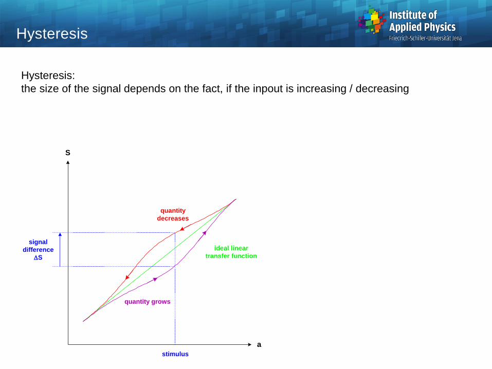
Hysteresis:
the size of the signal depends on the fact, if the inpout is increasing / decreasing
Hysteresis
S
a
ideal linear
transfer function
stimulus
signal
difference
S
quantity
decreases
quantity grows

Every sensor has a finite range of operation for the input stimulus
Limitations:
- upper limit: saturation
- lower limit: noise
Dynamic Range
signal S
0
stimulus a
dead
arealinear
range
saturation
range
amin
amax
Smax
Smin

Removed input:
- sensor reacts with a delay
- switch-on curve with characteristic
delay time
Alternative description:
- frequency response for periodic activation
- maximum acceptance frequency
Time Response
signal S
0time t
stimulus a
tstart
T
Smax
0.9 Smax
signal S
signal S
0
frequency ffmax90
Smax
0.9 Smax
signal S0.7 Smax
fmax70
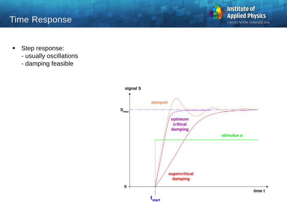
Step response: - usually oscillations - damping feasible
Time Response
signal S
0time t
stimulus a
tstart
Smax
supercritical
damping
optimum
critical
damping
damped

Photoconductive sensors:
inner and outer photo effect
photon extracts electron out of the binding
photo current measured
Important:
- materials
- gain
- geometry
Photo Diode
)(
e
Jph
s
1
0.5
0
400 600 800 1000 1200 1400
GaAs-
photocathode
CdS-
photoresistor
Si-
photoresistor
Ge-
photoresistor
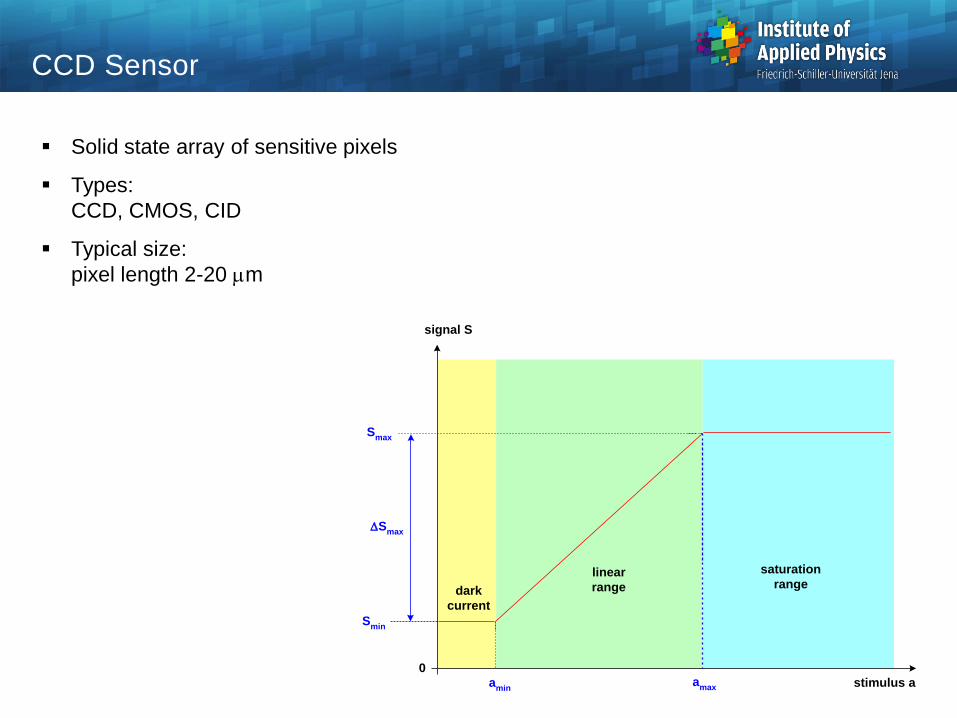
Solid state array of sensitive pixels
Types:
CCD, CMOS, CID
Typical size:
pixel length 2-20 mm
CCD Sensor
signal S
0
stimulus a
dark
current
linear
range
saturation
range
amin
amax
Smax
Smin
Smax

Color Sensor
Bayer mask of color sensor
Possible algorithms in signal processing:
Non-adaptive Adaptive
Nearest neighbor replication Edge scaling interpolation
Bilinear interpolation Interpolation with color
correction
Cubic convolution Variable number gradient
method
Smooth hue transition Pattern recognition
Smooth logarithmic hue
transition
Pattern matching interpolation
Ref: E. Derndinger
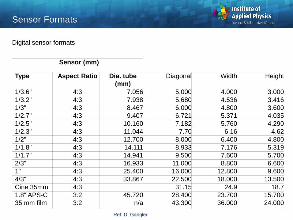
Sensor Formats
Digital sensor formats
Sensor (mm)
Type Aspect Ratio Dia. tube
(mm)
Diagonal Width Height
1/3.6" 4:3 7.056 5.000 4.000 3.000
1/3.2" 4:3 7.938 5.680 4.536 3.416
1/3" 4:3 8.467 6.000 4.800 3.600
1/2.7" 4:3 9.407 6.721 5.371 4.035
1/2.5" 4:3 10.160 7.182 5.760 4.290
1/2.3" 4:3 11.044 7.70 6.16 4.62
1/2" 4:3 12.700 8.000 6.400 4.800
1/1.8" 4:3 14.111 8.933 7.176 5.319
1/1.7" 4:3 14.941 9.500 7.600 5.700
2/3" 4:3 16.933 11.000 8.800 6.600
1" 4:3 25.400 16.000 12.800 9.600
4/3" 4:3 33.867 22.500 18.000 13.500
Cine 35mm 4:3 31.15 24.9 18.7
1.8" APS-C 3:2 45.720 28.400 23.700 15.700
35 mm film 3:2 n/a 43.300 36.000 24.000
Ref: D. Gängler

Architecture:
3 different types of carrier transport
1. full frame
2. interline
3. frame transfer
CCD Sensor
full frame interline transfer
2. read out serially
pixel by pixel
frame transfer
1. shift row-wise
downwards
1. shift to the right
by one column
2. shift read out
columns
downwards
not optically
active
1. shift row-wise
downwards
2. shift row-wise
downwards
3. read out serially
pixel by pixel
3. read out serially
pixel by pixel

Typical dimensions
Optical effect of arrays:
dead zone and change of acceptance angle
CCD-Sensors
Size
[mm]
Diagonal
[mm]
Pixel size
[mm]
Pixel number
12.8 9.6 16 16.7 20 768 480
8.8 6.6 11 11.4 13.8 768 480
6.4 4.8 8 8.33 10 768 480
4.8 3.6 6 6.25 7.5 768 480
3.2 2.4 4 4.17 5 768 480
active detector areas
CCD CCD CCD CCD
signal / loss
CCD CCD CCD CCD
signal
active detector areas
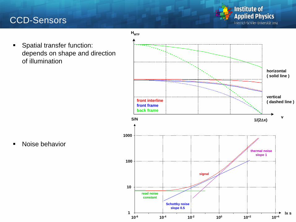
Spatial transfer function:
depends on shape and direction
of illumination
Noise behavior
CCD-Sensors
HMTF
v1/(2x)
front interline
front frame
back frame
horizontal
( solid line )
vertical
( dashed line )
10-6 10-4 10-2 100 10+2 10+4lx s1
S/N
10
100
1000
read noise
constant
Schottky noise
slope 0.5
thermal noise
slope 1
signal
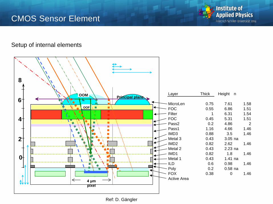
CMOS Sensor Element
Setup of internal elements
Layer Thick Height n
MicroLen 0.75 7.61 1.58
FOC 0.55 6.86 1.51
Filter 1 6.31 1.54
FOC 0.45 5.31 1.51
Pass2 0.2 4.86 2
Pass1 1.16 4.66 1.46
IMD3 0.88 3.5 1.46
Metal 3 0.43 3.05 na
IMD2 0.82 2.62 1.46
Metal 2 0.43 2.23 na
IMD1 0.82 1.8 1.46
Metal 1 0.43 1.41 na
ILD 0.6 0.98 1.46
Poly 0.2 0.58 na
FOX 0.38 0 1.46
Active Area
OOM
L
OOF
Principal plane
0
2
4
6
8
4 μm
pixel
Ref: D. Gängler

Chemical detector
Photons change silver salt atom
Size of grains defines spatial resolution
MTF depends on spectrum
Typical:
50% contrast at 100 Lp/mm
Contrast for limiting frequency
1000 Lp/mm
Photografic Film
HMTF
1
0.5
010 20 50 100 200
Log s in LP/mm
0.75

Photolayer darkening
Linearity in medium range of brightness
Description of sensitivity with the optical density D
Solarization at higher density
Photo Layer
)(HLog
D
D
log H
in Lux
fog
linear
range
solarization
= tan
0.1

Discrete pixelized detector:
sinc-transfer function
Detector Sampling
0.2 0.4 0.6 0.8 1 1.2 1.4 1.6 1.8 2 2.20
0.2
0.4
0.6
0.8
1
HMTF
cutoff
frequency
Nyquist-
frequency
1/Dpix
0
0.64

Low-pass filtering:
suppression of high-frequency signals
Numerical realization:
- Fourier spectrum limited
- smooth truncations filters to avoid
oszillations
Typical effects:
- side lobes
- reduced gradients
- higher frequencies damped
Well known filter solutions:
- rectangle
- Hanning
- Hamming
- Blackman
- Bartlett, Dreieck
Signal Filtering
I(x)
-1 -0.8 -0.6 -0.4 -0.2 0 0.2 0.4 0.6 0.8 1
0
0.2
0.4
0.6
0.8
1
x
measured
data
weak
smoothing
strong
smoothing

Signal Filtering
filter spectrum W() filter function W(x) linearfilter function log W(x)
logarithmic1
10-2
10-4
10-6
1
10-2
10-4
10-6
1
10-2
10-4
10-6
1
10-2
10-4
10-6
1
10-2
10-4
10-6
rectangle
Hanning
triangle
Hamming
Blackman

Fit of polynomial with order k and N points
Good conservation
of gradients
Features with higher
frequency content
preserved
Savitzky-Golay Filter
k = 15 k = 35 k = 61
N = 41
N = 81
N = 151
N = 251
N = 351
N = 491

Optimization of
1. polynomial order k
2. number of points N
Savitzky-Golay Filtering
N
5 10 15 20 25 30 35 40 45 50
20
40
60
80
100
120
140
160
180
200
220
240
k
limit
Nmin
limit
k = N
limit
N = Nges/4
k
N
Rms
Grenze
k = NGrenze
Nmin
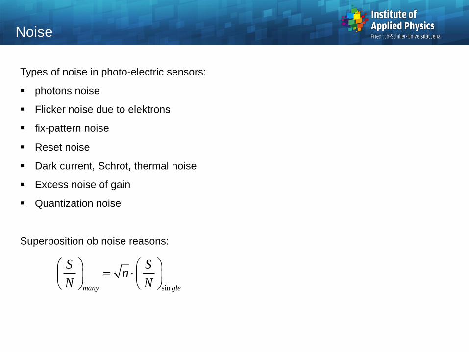
Types of noise in photo-electric sensors:
photons noise
Flicker noise due to elektrons
fix-pattern noise
Reset noise
Dark current, Schrot, thermal noise
Excess noise of gain
Quantization noise
Superposition ob noise reasons:
Noise
sinmany gle
S Sn
N N

Generation of noise in photo-eletric sensors
Noise
signal
quantum
noise
photo current
photo
effect
photoelectron.
noise
fixed pattern +
reset noise
electron
current
optional for
diode arrays
optional for
amplification
noise
thermal dark-
current noise
quantization
optional for
digitization
transit time
noise
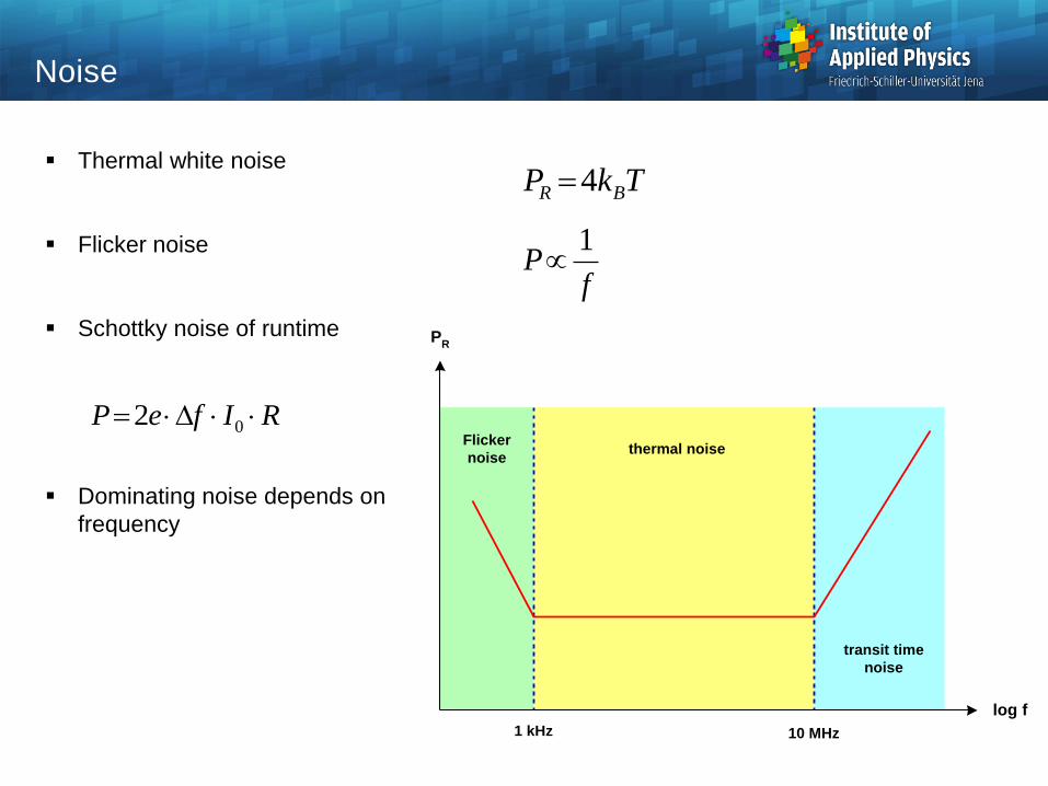
Thermal white noise
Flicker noise
Schottky noise of runtime
Dominating noise depends on
frequency
Noise
TkP BR 4
fP
1
RIfeP 02
log f
PR
Flicker
noisethermal noise
transit time
noise
1 kHz 10 MHz

Poisson statistics of photons:
quantum noise for small signal strengths
Width of distribution
Lock-in:
imprtovement of signal to noise ratio
by transform into low-noise band
Quantum Noise and Lock-in
NN N
f(N)
<N>
N = N
f
f(N)
1/f - noise
thermal noisesignal
bevor
signal
after
modulation
frequency
lock-in
transformation

Poisson noise
and white noise
Quantum Noise
10 % white
noise
10 % Photon
noise
original
signal

Characteristic:
Noise grows with
1. time of integration
2. size of detector area
Noise
1 10 100
1
10
100
Adetect
tintegral
SNR

Noise reduction and subtraction of background
Background Noise
0.1 0.2 0.3 0.4 0.5 0.6 0.7 0.8 0.9 1
10-4
10-3
10-2
10-1
100
10-4
10-3
10-2
10-1
100
filtered
data
original
data
intensity
Log w
signals
noise below
10 %


