
MANIPAL INSTITUTE OF TECHNOLOGY
Manipal – 576 104
DEPARTMENT OF ELECTRICAL & ELECTRONICS ENGG.
CERTIFICATE
This is to certify that Ms./Mr. …………………...……………………………………
Reg. No. …..…………………… Section: ……………… Roll No: ………………... has
satisfactorily completed the lab exercises prescribed for Electrical Circuits Lab
[E&E 2111] of Second Year B. Tech. Degree at MIT, Manipal, in the academic year
2015-2016.
Date: ……...................................
Signature Signature
Faculty in Charge Head of the Department

CONTENTS
LAB
NO. TITLE
PAGE
NO. REMARKS
COURSE OBJECTIVES AND OUTCOMES i
EVALUATION PLAN & INSTRUCTIONS TO THE STUDENTS i
COURSE PLAN ii
SIMULATION EXPERIMENTS
MODULE 1-MATLAB 1-14
1 MATLAB – TUTORIAL 1 15-18
2 MATLAB – TUTORIAL 2 19-25
3 MODELING WITH SIMULINK 26-28
MODULE 2-PSPICE 29-32
4 PSPICE-NETLIST 33-38
5 PSPICE -SCHEMATICS 39-41
HARDWARE EXPERIMENTS
6 SUPERPOSITION AND RECIPROCITY THEOREMS 42-46
7 THEVENIN‘S AND NORTON‘S THEOREMS 47-52
8 MAXIMUM POWER TRANSFER THEOREM 53-56
9
A. SELF AND MUTUAL INDUCTANCE OF A COIL
B. POWER, POWER FACTOR AND POWER FACTOR
IMPROVEMENT.
57-60
61-63
10 THREE PHASE POWER MEASUREMENT 64-68

Electrical Circuits Laboratory
i
Course Objectives
Use simulation tools like MATLAB/SIMULINK and PSPICE to solve
engineering problem
Apply network theorems for the analysis of given electrical systems
Measure power consumed by a three phase star/delta connected load
Improve power factor of the load using capacitor
Course Outcomes
At the end of this course, students will be able to
Implement simple electric circuits in MATLAB/SIMULINK platform to perform
steady state analysis and transient analysis
Design GUI using MATLAB
Implement electric circuits in PSPICE to perform steady state analysis and
transient analysis.
Verify network theorems like Thevenin, Superposition etc.
Measure self and mutual inductance of a coil and improve power factor of the coil
Measure 3 phase power for balanced and unbalanced load
Evaluation plan
Internal Assessment Marks : 60%
Continuous evaluation component (for each experiment):10 marks
The assessment will depend on punctuality, preparation, conduction, maintaining
the observation note and answering the questions in viva voce
Total marks of the10 experiments will be reduced to marks out of 60
End semester assessment of 3 hour duration: 40 %
INSTRUCTIONS TO THE STUDENTS
1. Students should carry the Lab Manual Book and Observation Book to every lab
session.
2. Be in time and follow the institution dress code.
3. Show the results to the instructors on completion of experiments and copy the
results in the Lab record.
4. For Hardware experiments, Get the circuit verified by the instructor before
switching on the supply.
5. The students should not go out of the lab without permission

Electrical Circuits Laboratory
Dept of E&E, MIT Manipal ii
Course Plan
ELE 2111: ELECTRICAL CIRCUITS LABORATORY [0 0 3 1]
Module I Circuit Simulation using MATLAB /
SIMULINK Introduction to MATLAB: Interactive computation,
script files, function files. Steady-state analysis of
circuits: Solution of algebraic equation.
Transient analysis of circuits: Solution of system
equations using ODE solvers. Introduction to GUIDE.
Introduction to SIMULINK and SIMSCAPE.
Week 1-3
Module II Circuit Simulation using PSPICE
Introduction to PSPICE, Steady state analysis of DC
circuits, single & three-phase AC circuits, and coupled
circuits.
Frequency response of circuits – series & parallel
resonance.
Week 4-5
Module III Circuits Hardware Experiments
Verification of Theorems: Superposition, Reciprocity,
Thevenin‘s, Norton‘s and Maximum power transfer
theorems.
Measurement of self and mutual inductances
Power, power factor and pf improvement, Three phase
power measurement
Week 6-10
Repetition Week 11
Test Week 12

Electrical Circuits Laboratory
Dept of E&E, MIT Manipal 1
Module I
CIRCUIT SIMULATION USING MATLAB/ SIMULINK
Introduction to MATLAB
MATLAB is a high-level language and interactive environment for numerical computation,
visualization, and programming. MATLAB helps to analyze data, develop algorithms, and
create models and applications. The language, tools, and built-in math functions enable to
explore multiple approaches and reach a solution faster than with spreadsheets or traditional
programming languages. MATLAB can be used for a range of applications, including signal
processing and communications, image and video processing, control systems, test and
measurement, computational finance, and computational biology. More than a million
engineers and scientists in industry and academia use MATLAB, the language of technical
computing.
Simulink is a block diagram environment for multi domain simulation and Model-Based
Design. It supports system-level design, simulation, automatic code generation, and
continuous test and verification of embedded systems. Simulink provides a graphical editor,
customizable block libraries, and solvers for modeling and simulating dynamic systems. It is
integrated with MATLAB, enable to incorporate MATLAB algorithms into models and
export simulation results to MATLAB for further analysis.
Getting started
Using Windows Explorer, create a folder user_name in the directory
c:\eclab\batch_index
For uniformity, let the batch_index be A1, A2, A3, B1, B2, or B3 and user_name be the
roll number
Invoke MATLAB
Running MATLAB opens the Matlab Desktop on your monitor. Of these the
Command window is the primary place where you interact with MATLAB. The
prompt >> is displayed in the Command window and when the Command window is
active, a blinking cursor should appear to the right of the prompt.
>> cd c:\eclab\batch_index\roll number % sets working directory
The working directory can also be selected using the Browse for folder icon on the
desktop
The desktop includes these panels: Current Folder — Access your files.
Command Window — Enter commands at the command line, indicated by the prompt (>>).
Workspace — Explore data that you create or import from files.
Command History — View or rerun commands that you entered at the command line.

Electrical Circuits Laboratory
Dept of E&E, MIT Manipal 2
MATLAB is available on a number of computing environments: Microsoft Windows, UNIX
operating systems such as Linux and Macintosh.
Number Display Formats
When MATLAB displays numerical results, it follows several rules. By default an integer
will be displayed as an integer and real number as real number with four digits to the right of
the decimal point. We can override this default behavior by specifying different formats as
given in the table below.
Table1: examples of number display formats
MATLAB Command pi comments
format short 3.1416 4 digits after decimal point
format long 3.141592653589793 15 digits after decimal point
format shortE 3.1416e+000 4 digits after decimal point plus
exponent
format longE 3.141592653589793e+000 15 digits after decimal point
plus exponent
format shortEng 3.1416 Best of format short or shortE
format longEng 3.141592653589793 Best of format long or longE
format hex 400921fb54442d18 Hexadecimal
Format blank 3.14 2 decimal digits
MATLAB Help
>> help inv
The online help system is accessible using the help command. Help is available for
functions eg. help inv. Demos and help can be invoked using the Help Menu at the top
of the window and from the Start icon at the bottom left of the Matlab Desktop.
Table 2: Common MATLAB functions Availability
Elementary math functions doc elfun
Data Analysis and Fourier transforms doc datafun
Elementary matrices and matrix manipulation doc elmat
Specialized math functions doc specfun
Help topics helpwin
Various MATLAB functions along with syntax and description can be obtained by typing
commands given in Table 2 to the command window.

Electrical Circuits Laboratory
Dept of E&E, MIT Manipal 3
Elementary Matrix Operations
To enter a matrix with real elements
A = [ 5 3 7; 8 9 2; 1 4.2 6e-2] A is a 3x3 real matrix
To enter a matrix with complex elements
B = [5+3j 7+8j; 9+2j 1+4j] B is a 2x2 complex matrix
Transpose of a matrix A_trans = A'
Determinant of a matrix A_det = det(A)
Inverse of a matrix A_inv = inv(A)
Matrix multiplication C = A * A_trans
Operators
Arithmetic operators
+ : Addition - : Subtraction
* : Multiplication / : Division
\ : Left Division ^ : Power
Relational operators
< : Less than <= : Less than or equal to
> : Greater than >= : Greater than or equal to
== : Equal ~= : Not equal
Logical operators
& : AND | : OR ~ : NOT
Array operations
Matrix operations preceded by a . (dot) indicates array operation.
Simple math functions
sin, cos, tan, asin, acos, atan, sinh, cosh ….
log, log10, exp, sqrt …
Special constants
pi, inf, i, j, eps …..
Control Flow Statements
for loop : for k = 1:m
.....
Electrical Circuits Laboratory
Dept of E&E, MIT Manipal 4
end
while loop : while condition
.....
end
if statement : if condition1
.....
else if condition2
.....
else
.....
end
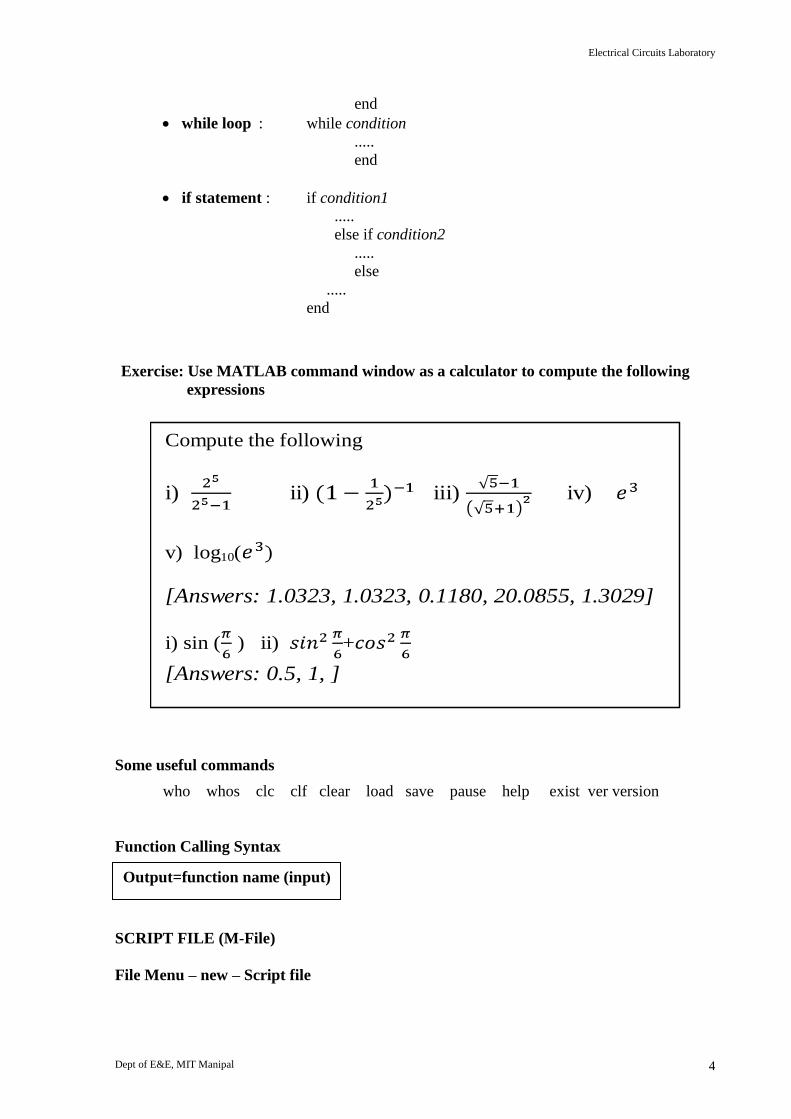
Exercise: Use MATLAB command window as a calculator to compute the following
expressions
Compute the following
i) ii) iii) iv)
v) log10(
[Answers: 1.0323, 1.0323, 0.1180, 20.0855, 1.3029]
i) sin ( ) ii) +
[Answers: 0.5, 1, ]
Some useful commands
who whos clc clf clear load save pause help exist ver version
Function Calling Syntax
SCRIPT FILE (M-File)
File Menu – new – Script file
Output=function name (input)

Electrical Circuits Laboratory
Dept of E&E, MIT Manipal 5
Will open a new M – file where one can type the program save as ex_eclab1.m (end with an
extension .m)
Note: It is important to note that an existing function name should not be used as a file
name.
Example: Find the power and energy 0.1H when the current and voltages are given by
Plot current, voltage, power and energy
% to plot current, voltage, power and energy
clear; clc;
t=0:0.01:2;
for i=1:length(t)
if t(i)<=0
I(i) = 0;
v(i)=0;
elseif t(i)>0 &t(i)<=1
I(i)=20*t(i);
v(i)=2;
else t(i)>=1
I(i)=20;
v(i)=0;
end
end
L=0.1;
I;v;P=I.*v; W=0.5*L*I.^2; plot(t,I,t,v,t,P,t,W)
The script file can also be executed from the Save and Run command in Debug Menu of the
MATLAB Editor.
Exercise: plot the power and energy stored in a 0.1H inductor when
for
The ‘DOT’ preceding the standard *, /, ^… gives element by element operation
The colon is one of the most useful operators in MATLAB. It can create vectors,
subscript arrays, and specify for iterations.

Electrical Circuits Laboratory
Dept of E&E, MIT Manipal 6
Array operations
EXAMPLE:
Example: enter a 5x5 matrix using the function ‗magic‘ and do the following
A(:,j) jth
column of A
A(i,:) ith
row of A
A(:,:) same as A
A(j:k) A(j), A(j+1),...,A(k)
A(:,j:k) A(:,j), A(:,j+1),...,A(:,k).
A(:,:,k) kth
page of three-dimensional array A.
A(i,j,k,:)
vector in four-dimensional array A. The vector
includes A(i,j,k,1), A(i,j,k,2), A(i,j,k,3), and so on.
A(:) all the elements of A, regarded as a single column.
A(:,2)=[] A (1,:)=[] Deletion of rows and columns
B = A(5, 1:5); Read columns 1-5 of row 5
B = A(2:2:4, 1:5);
Read columns 1-5 of rows 2 & 4.
B = A(:, 1:5);
Read columns 1-5 of all rows
%array-array mathematics
Q1=A+A;Q2=A-A;Q3=A.*A;Q4=A./A;
%array Element by element
%exponentiation
P=A.^2
%reciprocal
R=1./A
%raise 2 to the power of each element
%of array
T=2.^A
size(A)
ones(size(A))
zeros(size(A))
zeros(2,5)
%identity matrix
eye(3)
%uniformly distributed random array
%b/w 0 &1
rand(3)
%optimum array addressing
d=pi;
O=repmat(d,3,4)
%Array Manipulation
A=[1 2 3;5 6 7;8 9 2]
%set element in 2nd
row 3rd
column to 0
A(2,3)=0
clc; clear;
%array operations
%enter row vector
A=[0 2 4 6 8 10 12 14 16 18 20]
%or
A=0:2:20
%column vector
A1=A'
A2=[0;2;4;6;8;10;12;14;16;18;20]
%array elements can be accessed using subscripts
B=A(5)
% access a block of elements at one time
C=A(1:5)
D=A(6:end)
%reverse order
E=A(3:-1:1)
%to extract the elements in any order
F=A([4 8 1 10])
A3=linspace(0,20,11)
A4=logspace(-1,2,10)
%complex column vector
G=A2+A2*j
%array of 2 rows and 4 columns
H=[2 3 4 5;7 8 9 6]
%scalar - array operations
%apply the operation to all elements of the array
S1=2*A; S2=2-A; S3=2+A;S4=A/2;

Electrical Circuits Laboratory
Dept of E&E, MIT Manipal 7
Relational Operators
The relational operators are <, >, <=, >=, ==, and ~=. Relational operators perform element-
by-element comparisons between two arrays. They return a logical array of the same size,
with elements set to logical 1 (true) where the relation is true, and elements set to logical 0
(false) where it is not. If one of the operands is a scalar and the other a matrix, the scalar
expands to the size of the matrix.
Examples :
Logical Operators: AND ( &), OR( |), NOT( ~)
These operators are commonly used in conditional statements. The expression operands for
AND, OR, and NOT are often arrays of non-singleton dimensions. The MATLAB software
performs the logical operation on each element of the arrays. The output is an array that is the
same size as the input array or arrays. Table 3 shows the output of AND, OR, and NOT
statements that use scalar and/or array inputs. In the table, S is a scalar array, A is a non-
scalar array, and R is the resulting array. If two or more operations have the same precedence,
the expression is executed in order from left to right. In order to avoid compatibility problem
between different versions of MATLAB, it is better to practice parentheses according to the
precedence. Table 4 shows the operation and order of precedence.
%relational operations
A = [0.53 0.67 0.01 0.38 0.07 0.42 0.69];
X=0.02; X>=A;
all(A>=X)
any(A>=X)
find(A)%non-zero elements
find(A>X)
find(0 < A & A < 0.1*pi)
strcmp('Yes', 'No')%returns 0
strcmp('Yes', 'Yes') %returns 1
A = {'MATLAB','SIMULINK'; ...
'Toolboxes', 'MathWorks'};
B = {'Handle Graphics', 'Real Time Workshop'; ...
'Toolboxes', 'MathWorks'};
C = {'handle graphics', 'Signal Processing'; ...
' Toolboxes', 'MATHWORKS'};
strcmp(A,C)%compare with sensitivity to case
strcmpi(B,C)%compare without sensitivity to case

Electrical Circuits Laboratory
Dept of E&E, MIT Manipal 8
Table 3: Description and output of logical operators
Operation Result Description
S1 & S2 R = S1 & S2 AND
If both are true ,the result is
true(1), otherwise the result
is false(0)
S & A R(1) = S & A(1); ...
R(2) = S & A(2); ...
A1 & A2 R(1) = A1(1) & A2(1);
R(2) = A1(2) & A2(2); ...
S1 | S2 R = S1 | S2 OR
If either one or both are true
the result is true(1),
otherwise the result is
false(0)
S | A R(1) = S | A(1);
R(2) = S | A(2); ...
A1 | A2 R(1) = A1(1) | A2(1);
R(2) = A1(2) | A2(2); ...
~S R = ~S NOT
Give 1 if the operand is
false(0) and 0 if the operand
is true(1)
~A R(1) = ~A(1);
R(2) = ~A(2), ...
xor(A1,A2) R(1)=xor(A1(1),A2(1)),
R(2)=xor(A1(2),A2(2)),…
Give 1 if one operand only
is true , otherwise 0
A&&B
Short circuit operators B is evaluated only of A is true
Returns logical 1 (true) if
both inputs evaluate to true,
and logical 0 (false) if they
do not.
A||B Returns logical 1 (true) if
either input, or both, evaluate
to true, and logical 0 (false)
if they do not.
Table 4: Order of Precedence of Operation
Operation Order of
precedence Parentheses ( for nested parentheses , inner
have precedence)
1 (highest)
Transpose (.'), power (.^), complex
conjugate transpose ('), matrix power (^)
2
Exponentiation 3
Logical NOT (~) 4
Multiplication , Division 5
Addition , subtraction 6
Relational operators (<, >, >=, <=, ==,~=) 7
Logical AND (&) 8
Logical OR (|) 9
Short circuit AND 10
Short Circuit OR 11

Electrical Circuits Laboratory
Dept of E&E, MIT Manipal 9
Examples on logical operators
Graphics Using MATLAB MATLAB is capable of producing two dimensional x-y plots and three-dimensional plots,
displaying images and even creating and playing movies. MATLAB plotting functions and
tools direct their output to a figure window. Each figure is a separate window that can dock in
the desktop, and collect together with other plots in a Figure Group. The most common for
plotting 2 dimensional data is the plot function which sets of data arrays on appropriate axes
and connects the points with straight line. The plot function uses a default line style and color
to distinguish the data sets plotted in the graph. Change the appearance of these graphic
components or add annotations to the graph helps to present the data in a particular way. The
following code illustrates the basic components of a graph.
Examples:
% examples of logical operators
x=-3; y=6;
-5<x<-1 %returns 0
-5<x&x<-1 % returns 1
~(y<7) % returns 0
~y<7 %returns 1
~((y>=8)|(x<-1))% returns 0
~(y>=8)|(x<-1)% returns 1
A = [0 1 1 0 1];
B = [1 1 0 0 1];
A&B
A|B
~A
xor(A,B)
P=28;Q=21
C=bitand(A,B)% bitwise and operation
b=1;a=20
x = (b ~= 0) && (a/b > 18.5)
b=0;a=20
x = (b ~= 0) && (a/b > 18.5)
% To plot y = 2x for -10 x 10
clear; clc;
x=-10:0.01:10;
y=x.^2;
plot(x,y,'r')
xlabel('x')
ylabel('y')
title('plot of y=x^2')

Electrical Circuits Laboratory
Dept of E&E, MIT Manipal 10
Exercise: Create line plot using specific line width, marker color, and marker size by
programming also using interactive plottools
Functions to generate data points x=linspace(1,100,10), generates 10 equally spaced points between 1 &100
x=logspace(-1,2,100), generates 100 logarithmically equally spaced points between to
Try the following 2D plotting functions Line Graphs: plot, plotyy, loglog, semilogx,semilogy,stairs, contour,ezplot,ezcontour
Bar Graphs: bar, barh, hist, pareto, errorbar,stem
Area Graphs: area, pie, fill, contour, image, pcolor, ezcontourf
Direction Graphs: feather, quiver, comet
Radial Graphs: polar, rose, compass, ezpolar
Scatter Graphs: scatter, spy, plotmatrix
Example of a filled circle
Exercise: obtain the following as subplots using suitable functions
-4 -2 0 2 40
0.2
0.4
0.6
0.8
1
0 1 2 3 4-0.2
0
0.2
0.4
0.6
0.25
0.5
30
210
60
240
90
270
120
300
150
330
180 0
11%
33%
6%
28%
22%
clc;clear;
t=0:pi/20:2*pi;
fill(cos(t),sin(t),'r',0.8*cos(t),0.8*sin(t),'y')
axis square
Electrical Circuits Laboratory
Dept of E&E, MIT Manipal 11
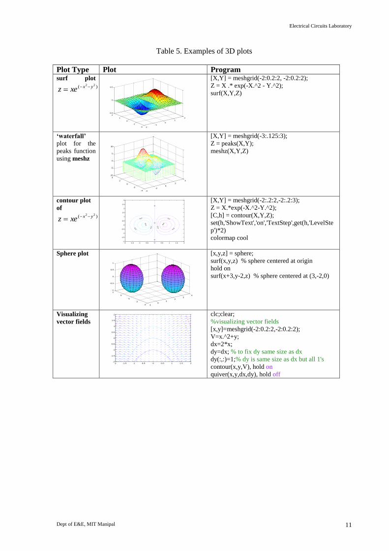
Table 5. Examples of 3D plots
Plot Type Plot Program surf plot
)( 22 yxxez
-2
-1
0
1
2
-2
-1
0
1
2-0.5
0
0.5
[X,Y] = meshgrid(-2:0.2:2, -2:0.2:2);
Z = X .* exp(-X.^2 - Y.^2);
surf(X,Y,Z)
‘waterfall’
plot for the
peaks function
using meshz
-4
-2
0
2
4
-4
-2
0
2
4-10
-5
0
5
10
[X,Y] = meshgrid(-3:.125:3);
Z = peaks(X,Y);
meshz(X,Y,Z)
contour plot
of
)( 22 yxxez
-0.4
-0.2 -0.2
-0.2
00
0
0.2
0.2
0.2
0.4
-2 -1.5 -1 -0.5 0 0.5 1 1.5 2-2
-1.5
-1
-0.5
0
0.5
1
1.5
2
2.5
3
[X,Y] = meshgrid(-2:.2:2,-2:.2:3);
Z = X.*exp(-X.^2-Y.^2);
[C,h] = contour(X,Y,Z);
set(h,'ShowText','on','TextStep',get(h,'LevelSte
p')*2)
colormap cool
Sphere plot
-10
12
34
-3
-2
-1
0
1-1
-0.5
0
0.5
1
[x,y,z] = sphere;
surf(x,y,z) % sphere centered at origin
hold on
surf(x+3,y-2,z) % sphere centered at (3,-2,0)
Visualizing
vector fields
-2 -1.5 -1 -0.5 0 0.5 1 1.5 2-2
-1.5
-1
-0.5
0
0.5
1
1.5
2
clc;clear;
%visualizing vector fields
[x,y]=meshgrid(-2:0.2:2,-2:0.2:2);
V=x.^2+y;
dx=2*x;
dy=dx; % to fix dy same size as dx
dy(:,:)=1;% dy is same size as dx but all 1's
contour(x,y,V), hold on
quiver(x,y,dx,dy), hold off

Electrical Circuits Laboratory
Dept of E&E, MIT Manipal 12
Polynomials, Curve Fitting & interpolation Example: Consider the polynomial
Curve fitting
Note: Also use Basic Fitting tool & Curve fitting App
Examples on Interpolation
Function Type Example
Interp1
Y1=Interp1(X,Y,XI)
1D interpolation x = 0:10; y = sin(x); xi = 0:.25:10;
yi = interp1(x,y,xi);
plot(x,y,'o',xi,yi)
Interp2
ZI = interp2(X,Y,Z,XI,YI)
2D interpolation [x,y,z] = peaks(10); [xi,yi] = meshgrid(-
3:.1:3,-3:.1:3);
zi = interp2(x,y,z,xi,yi);
mesh(xi,yi,zi)
%Polynomials with MATLAB
P=[1 -10 50 -20 -70 40]; %enter the polynomial coefficients
polyval(P,5); %evaluate the polynomial for x=5
x=-2:0.01:4;
y=polyval(P,x); % generate y for x = -2 to 4
plot(x,y); %plot the polynomial
R=roots(P); %roots of the polynomial
poly(R); % to find polynomial coefficients
P1=[0 0 2 0 -4 -8];
P2=P+P1; %addition
P3=conv(P,P1); %multiplication
[q,r]=deconv(P3,P); %division
k=polyder(P); %Derivative
k1=polyder(P,P1); %derivative of P*P1
[N,D]=polyder(P3,P); %Derivative of P3/P
I=polyint(P); %integrate the polynomial
clc; clear;
%example of curve fitting
x=[-5 -4 -2.2 -1 0 1 2.2 4 5 6 7];
y=[0.1 0.2 0.8 2.6 3.9 5.4 3.6 2.2 3.3 6.7 8.9];
p=polyfit(x,y,6);
f=polyval(p,x);
plot(x,y,'b',x,f,'r')
table=[x; y; f;y-f]'

Electrical Circuits Laboratory
Dept of E&E, MIT Manipal 13
Example 2:
%To plot a function its integral
and derivative
syms x;
f=sin(x)/x;
figure(1)
ezplot(f,[-15, 15])
F=int(f,x);
figure(2)
ezplot(F,[-15, 15])
G=diff(F)
figure(3)
ezplot(G,[-15, 15])
Symbolic Computation Symbolic Math Toolbox provides functions for solving and manipulating symbolic math
expressions and performing variable-precision arithmetic. It allows analytically perform
differentiation, integration, simplification, transforms, and equation solving. Also generate
code for MATLAB, Simulink, and Simscape from symbolic math expressions.
To declare variables x and y as symbolic objects use the syms command:
syms x y
diff; int ;solve; ezplot; ezplot3;ezsurf; dsolve;
Example 1
clc; clear;
%to declare the variables
syms x y w s z n S
(x-y)*(x+y)
expand(ans)
factor(ans)
w=(x-y)*(x+y)
subs(w,{x,y},{[1,2]})
%inverse laplace transform
ilaplace(1/(s-1))
%inverse z transform
iztrans(z/(z-2))
[x,y] = solve('x^2*y^2 - 2*x - 1 = 0','x^2 - y^2 - 1 = 0')
x=double(x); y=double(y);

Electrical Circuits Laboratory
Dept of E&E, MIT Manipal 14
Example: Current signal is given; find the voltage across the capacitor of 2F
Hint:
%generate a test signal
[u,t]=gensig('square',5,30,0.1);
H=tf(1,[2 0]);
lsim(H,u,t)
REFERENCES
1. William Palm III, Introduction to MATLAB 7.4 for Engineers, MGH 2007.
2. D. Hanselman and B. Littlefield, Mastering MATLAB , Prentice Hall, 2011
3. Brian R. Hunt, Ronald L. Lipsman, Jonathan M. Rosengurg, A Guide to MATLAB,
Cambridge University Press, 2011.
4. Amos Gilat, MATLAB - An Introduction with Applications, Wiley India Edition, 2010.
5. Rudra Pratap, Getting Started with MATLAB – A Quick Introduction for Scientists and
Engineers, Oxford University Press, 2010.
6. Shampine I.F, Solving ODEs with MATLAB, Cambridge University Press, 2003.
7. www.mathworks.com
TAH & Installation Manipal Institute of Technology is the first Institute in the country that has implemented a
campus-wide license for the MATLAB and Simulink product families. The campus-wide
license ensures access to world-class research infrastructure for our students, research
scholars and faculty members.

Electrical Circuits Laboratory
Dept of E&E, MIT Manipal 15
TUTORIAL 1
Objective: Solution of first and second order system equations using MATLAB(numerical)
and symbolic math toolbox(symbolic)
1. Find the loop currents of the circuit given in Fig. 1.1
VVo 10
+-
1I 2I
101R 103R
52R 204R
Fig. 1.1 Using Mesh Analysis
0
10
355
515
2
1
I
I
Sample Solution (using command line editor)
Z = [15 -5;-5 35]; v = [10; 0]; i = inv(Z) * v; Results: I1= 07, I2= 0.1
Using Symbolic math toolbox
syms I1 I2;
e1='15*I1-5*I2=10'; e2='-5*I1+35*I2=0'; s=solve(e1,e2,'I1','I2'); I=[s.I1,s.I2];

Electrical Circuits Laboratory
Dept of E&E, MIT Manipal 16
i(t)V=1
R =1
t=0
10 mF
2. Find the loop currents & node voltages of the circuit given in Fig. 1.2
(Write script files for solution) using command ‘inv’ and also using ‘solve’
Fig. 1.2
3. Find the transient response of the circuit given in Fig. 1.3
Given:
Sample Solution : (illustration of for loop)
clear; clc; disp(' RC transient analysis') v = input(' Enter source voltage : '); r = input(' Enter value of resistance :'); c = input(' Enter value of capacitor: '); T = r*c;
fprintf('\n The results are : \n\n') disp('t (sec) i (A) v_c (V)') for n = 1:10
t(n) = (n-1)*T/2; Fig.1.3
i(n) = (v/r)* exp(-t(n)/T); v_c(n) = v* (1 - exp(-t(n)/T)); fprintf('%6.4f\t%6.4f\t%6.4f\n', t(n),i(n),v_c(n))
end;
Colon operator: The colon operator is useful for creating index arrays, creating vectors of
evenly spaced values, and accessing sub-matrices. A regularly spaced vector of numbers is
obtained by means of
n = initial value : increment : final value
RCwhereeVtv
eR
Vti
t
c
t
1)(
)(

Electrical Circuits Laboratory
Dept of E&E, MIT Manipal 17
Sample Solution : (generating vectors)
clear; clc;
disp(' RC transient analysis')
v = input(' Enter source voltage : '); r = input(' Enter value of resistance : '); c = input(' Enter value of capacitor : '); T = r*c; fprintf('\n The results are : \n\n') disp('t (sec) i (A) v_c (V)') t = 0 : 0.5*T : 5*T; % start value : increment : final value i = (v/r) * exp(-t/T); v_c = v * (1 - exp(-t/T)); % To output the results in tabular form A = [t; i; v_c]; % concatenates the vectors fprintf('%6.4f\t%6.4f\t%6.4f\n', A);
4. The switch shown in the diagram in Fig.1.4 has been in position ‘a’ for long time.
At t = 0, the switch is moved to position ‘b’ where it remains for 2 s and then moves
back to position ‘a’, where it remain indefinitely.
i. Obtain analytical expression for vc(t) and ic(t) for all t
ii. Use MATLAB to obtain plots vc(t) versus time and current ic(t) versus time over
the range 0 s ≤ t ≤ 10 s
Fig 1.4
5. Plot the inductor current and the capacitor voltage for time, 0 t 10s, of an RLC
series circuit with R = 1, L = 1H, & C = 10mF connected to a dc source of 10V
through a switch. The switch is closed at t = 0 & the circuit elements are initially
relaxed.
Discussion:
The RLC circuit can be described by the following KVL equations in terms of the state
variables vc and i, where vc is the voltage across the capacitor and i is the current through
the inductor.
+-
71R
12R33R
FC 5.0
VVo 100
a
b )(tic

Electrical Circuits Laboratory
Dept of E&E, MIT Manipal 18
'
'
c
c
Cvi
VvLiRi
%solution
clc;clear;
syms I(t) vc(t)
V=10;R=1;C=.01;L=1;
[I(t),vc(t)]=dsolve(diff(I)==(V/L)-(R/L)*I-(vc/L),diff(vc)==(1/C)*I,...
I(0)==0,vc(0)==0);
%[I(t),vc(t)]=dsolve(diff(I)==1-I-vc,diff(vc)==I,I(0)==0,vc(0)==1)
I=simplify(I)
vc=simplify(vc)
figure(1)
ezplot(I)
figure(2)
ezplot(vc)

Electrical Circuits Laboratory
Dept of E&E, MIT Manipal 19
TUTORIAL 2
Objective: Solution of first and second order system equations using Ordinary Differential
Equation (ODE) solvers and introduction to GUIDE.
Function File:
A function file is also an m-file, just like a script file except it has a function definition line at
the top that defines the input and output explicitly. function <output_list> = fname <input_list>
Save the function file as fname.m The filename will become the name of the new command
for MATLAB. Variables inside a function are local. Use global declaration to share variables.
1. Plot the dc transient response of a series RL circuit with R = 1 , L = 1 H, and
V=10 V. Switch is closed at t = 0.
Discussion:
The RL circuit can be described by the following KVL equations in terms of the state
variable i, where i is the current through the inductor.
VLiRi '
In order to use the MATLAB function ode23, the first order differential equations must be
placed in a .m file that returns the derivative of the state variable. The equation is:
ixwhereLRxVx /)('
Sample Solution
% Transient analysis RL series circuit % Solution using Ordinary Differential Equation (ODE) solver "ode23" % This program uses the function "rl_sys" global V R L; % define circuit parameters V=10; R=1; L=1; % define initial conditions IL0 x0=0; % define solution parameters t0=0; tf=10; tspan=[t0,tf]; % Numerical integration using MATLAB function "ode23" % User defined function "rl_sys" describes the system [t,x]=ode23('rl_sys',tspan,x0); % o/p results plot(t,x); %************************************************************************************

Electrical Circuits Laboratory
Dept of E&E, MIT Manipal 20
% open a new function file by name rl_sys.m % function "rl_sys" describes the system function xdot = rl_sys(t,x); global V R L; xdot=(V-R*x)/L; %************************************************************************************
2. Plot the dc transient response of a series RC circuit with R = 1 , C = 1mF, and
V = 1V. Switch is closed at t = 0. Measure Vc at t = 1s.
global V R C V=1; R=1; C=1e-3; options = odeset('RelTol',1e-4,'AbsTol',1e-4); [t,VC] = ode23(@RC,[0 10],[0],options); % o/p results plot(t,VC); %************************************************************************************ %function file %rc.m function vcdot=RC(t,VC) global V R C; vcdot=(V-VC)/(R*C);
%************************************************************************************
3. Obtain the capacitor voltage vo(t) and the current i(t) for 0 t 2 second. Circuit is
initially relaxed. At t=0, the switch is closed to position 1 and at t=0.5s the switch is
moved to position 2.
Fig.2.1
%Example: RC with switch clc; clear; global V R C; V=10;R=1;C=100e-3; options=odeset('RelTol',1e-6,'AbsTol',1e-6); %switch in position 1 VCi1=0; [t1,VC1]=ode45(@RC,[0 0.5],VCi1,options); I1=(V-VC1)./R; %switch in position 2 V=-20;
1
2
10 V 20 V
1 ohm
100 mFi(t)
Fig 9_2

Electrical Circuits Laboratory
Dept of E&E, MIT Manipal 21
for k=1:length(t1) if (t1(k)==0.5) VCi2=VC1(k); end end [t2,VC2]=ode45(@RC,[0.5 2],VCi2,options); I2=(V-VC2)./R; VC=[VC1;VC2];t=[t1;t2];I=[I1;I2]; plot(t,I,t,VC) grid;
Exercise: Use Publish to get the report in html/ pdf format
4. Plot the dc transient response of a series RC circuit with R = 1 , C = 1 F, and
V = 10 V. Switch is closed at t = 0 and Vc(0) = -5 V. Measure Vc at t = 2s.
ixvxwhereLRxxVx
Cxx
c
2121
2
, ,/)(
/
'
2
'
1
global V R L C; % define circuit parameters V=10; R=1; L=1; C=10e-3; % define initial conditions VC0=0; IL0=0; x0=[VC0;IL0]; % define solution parameters t0=0; tf=10; tspan=[t0,tf]; % Numerical integration using MATLAB function "ode23" % User defined function "rlc_sys" describes the system [t,x]=ode23('rlc_sys',tspan,x0); % o/p results plot(t,x); grid; %********************************************************************** % rlc_sys.m % function "rlc_sys" describes the system function xdot = rlc_sys(t,x); global V R L C; xdot=[x(2)/C;(-x(1)-R*x(2)+V)/L]; %************************************************************************************
Graphical User Interface (GUI) Design a GUI that will add together two input numbers and displays answer in a designated
text field.
GUIDE - Graphical User Interface Development Environment.
To invoke GUIDE from MATLAB command window
>>guide
Create a blank GUI and drag & drop the required objects on to the layout editor.

Electrical Circuits Laboratory
Dept of E&E, MIT Manipal 22
GUI Design Steps:
1. Type guide in the command window and this will open the GUIDE QUICK START
window. Choose the first option Blank GUI (Default) and click OK to open the layout
editor.
2. Drag and drop Two Edit Text components (for two input numbers), Three Static
Text components (for +, = and result field) and a Pushbutton component (for
addition operation) to the GUI by clicking on the respective component icon.
Rearrange the components accordingly.
3. Edit the properties of each of the components by double clicking on it. This will open
the Property Inspector Window. In the Property Inspector Window, edit the string
parameter appropriately (say the string parameter of two Edit Text components must
be set to 0, the static Text components to +, = and 0 and Pushbutton to Add). Also
observe the tag parameter of each of these components as these will be used in GUI
callbacks code.
4. Save the designed GUI and this will open the automatically generated .m file.
5. Within the .m file, go to function pushbutton1_Callback and type the
following code: Finally, execute the GUI program by pressing the icon on the GUIDE editor
and test the GUI by inputting some numbers.
Congratulations on creating your first GUI!!!!

Electrical Circuits Laboratory
Dept of E&E, MIT Manipal 23
Num1= get(handles.edit1,'String');
Num2 = get(handles.edit2,'String');
total = str2num(Num1) + str2num(Num2);
c = num2str(total);
set(handles.text3,'String',c);
6. Modify the above GUI and make a scientific calculator arithmetic, trigonometric
and logarithmic functions.
7. Create a GUI to show the addition of two sinusoidal components with different
frequencies.

Electrical Circuits Laboratory
Dept of E&E, MIT Manipal 24
% Get user input from GUI
f1 = str2double(get(handles.f1_input,'String'));
f2 = str2double(get(handles.f2_input,'String'));
t = eval(get(handles.t_input,'String'));
% Calculate data
x = sin(2*pi*f1*t) + sin(2*pi*f2*t);
y = fft(x,512);
m = y.*conj(y)/512;
f = 1000*(0:256)/512;
% Create frequency plot in proper axes
plot(handles.frequency_axes,f,m(1:257))
set(handles.frequency_axes,'XMinorTick','on')
grid on
% Create time plot in proper axes
plot(handles.time_axes,t,x)
set(handles.time_axes,'XMinorTick','on')
grid on
8. Create a GUI as given below to plot different 3D graphs with options to change
shading, colormap and axis

Electrical Circuits Laboratory
Dept of E&E, MIT Manipal 25
Assignment:
1. Plot the inductor current and the capacitor voltage for time, 0 t 10s, of an RLC
series circuit with R = 1, L = 1H, & C = 10mF connected to a dc source of 10V
through a switch. The switch is closed at t = 0 & the circuit elements are initially
relaxed.( using ode solver)
2. Steady- state condition exist in the network shown in figure below at t = 0-, when
the V2 =10 V is connected to the RL circuit. At t = 0+, the switch is moved
downward and the source V1 is then connected to the RL circuit, where it remains
for t ≥ 0.
i. Write and solve theoretically the differential loop equation for current i(t), and
the voltage vR(t) and vL(t) for t ≥ 0.
ii. Create the script file RL_IC that returns the solution for part 1 by using
MATLAB symbolic solver dsolve.
iii. Repeat part 2 by using the MATLAB numerical solver ode45.
iv. Also obtain the plots of i(t), vR(t) and vL(t) versus t.
+-
2R
HL 1
VV 201
b
)(ti+-VV 102
0t
Fig 2.2
3. Create GUI for transient analysis with one pushbutton for RL, one for RC and one
for RLC circuit. Enter the filename which is used to solve RL circuit (Q.No 1) in the
pushbutton callback meant for RL. Use global declaration to share variables.

Electrical Circuits Laboratory
Dept of E&E, MIT Manipal 26
TUTORIAL 3
Objectives: Transient Analysis of simple circuits using SIMULINK and SIMSCAPE.
SIMULINK - Graphical modeling, dynamic system simulation
To invoke SIMULINK from MATLAB Command Window
>> simulink or
In File menu, Select New Model
Draw the block schematic in the worksheet by copying the components from
Simulink library.
Set simulation parameters and then start simulation. After the simulation click on
scope to view the result.
1. An RLC series circuit with R = 1, L = 1H, & C = 10mF is connected to a dc
source of 10V through a switch. Plot the inductor current and the capacitor voltage
for time, 0 t 10s, if the switch is closed at t = 1s & the circuit elements are
initially relaxed. Repeat the question taking R=20 and 100.
Fig. 3.1
2. Using SIMULINK, obtain the capacitor voltage vo (t) and the current i(t) for
0 t 2s. Circuit is initially relaxed. At t=0, the switch is closed to position 1 and at
t=0.5s the switch is moved to position 2.
Fig.3.2
output
To WorkspaceStep
Scope
Mux
s
1
Integrator1
s
1
Integrator
1/C
Gain2R
Gain1
1/L
Gain
1
2
10 V 20 V
1 ohm
100 mFi(t)
Fig 9_2

Electrical Circuits Laboratory
Dept of E&E, MIT Manipal 27
Fig.3.2.1
3. Find the inductor current and capacitor voltage if the switch is moved to position 1
at time t=0s and switched to position 2 at time t=2s. Initial capacitor voltage
Vc(0)= -20 V.
+-VVo 100
I
FC 001.0
200cR
HL 5513.0
1LR
a
b
Fig.3.3
Fig.3.3.1
Electrical Circuits Laboratory
Dept of E&E, MIT Manipal 28
4. Plot the transient response (0 t 10s) of a series RL circuit with R = 1 ,
L = 100mH and square wave excitation with V= 10V, period 1s and 50% duty cycle.
5. Plot the dc transient response of a series RC circuit with R = 1, C = 1 F and
V= 10 V. Switch is closed at t = 0 and Vc (0) = -5 V. Measure Vc at t = 2s. Create
subsystem and mask it.
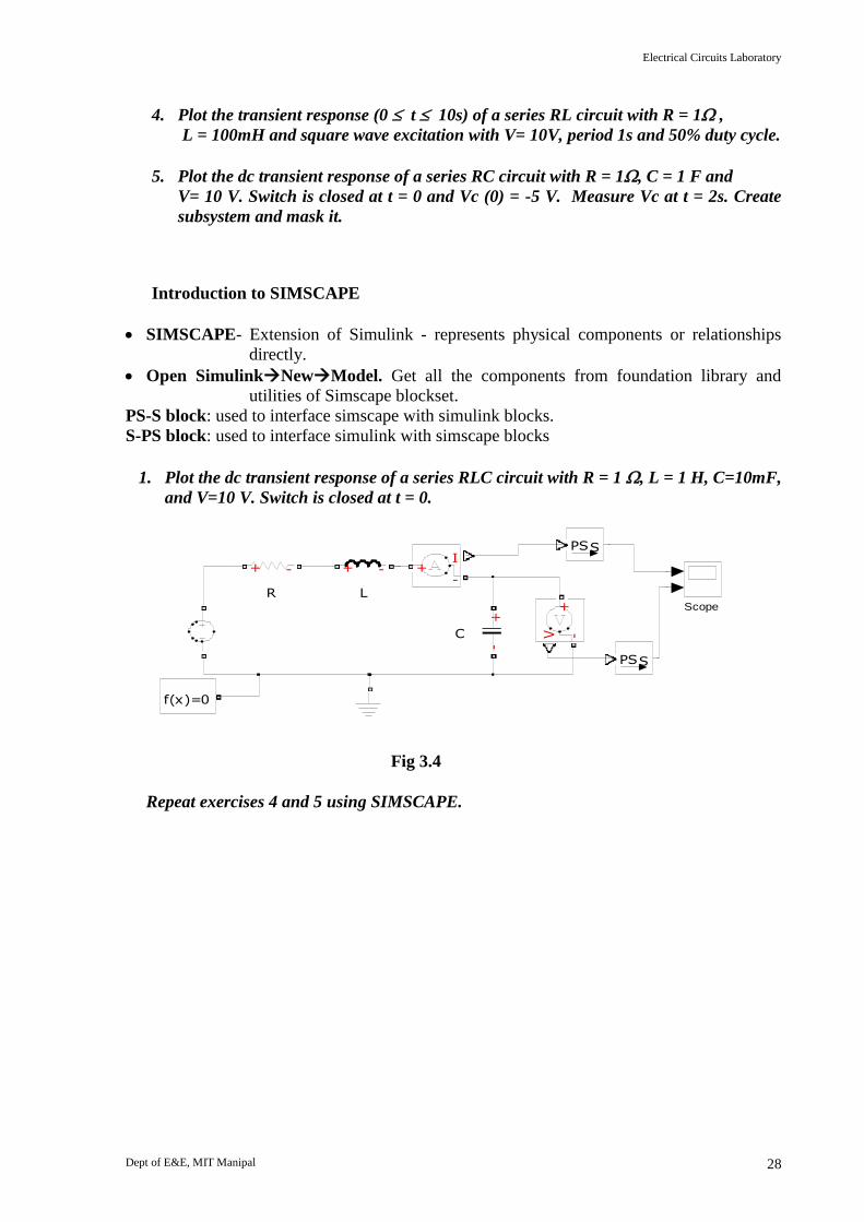
Introduction to SIMSCAPE
SIMSCAPE- Extension of Simulink - represents physical components or relationships
directly.
Open SimulinkNewModel. Get all the components from foundation library and
utilities of Simscape blockset.
PS-S block: used to interface simscape with simulink blocks.
S-PS block: used to interface simulink with simscape blocks
1. Plot the dc transient response of a series RLC circuit with R = 1 , L = 1 H, C=10mF,
and V=10 V. Switch is closed at t = 0.
FIFf
Fig 3.4
Repeat exercises 4 and 5 using SIMSCAPE.
+V -
f(x)=0
Scope
R
+ -
PSS
PSS
L
+ - +I
-
C
+-
Electrical Circuits Laboratory
Dept of E&E, MIT Manipal 29
Module II
CIRCUIT SIMULATION USING PSPICE What is PSPICE?
SPICE is an acronym for Simulation Program with Integrated Circuit Emphasis and
PSPICE is a PC version of SPICE. The program SPICE was developed at University of
California; Berkeley in early 1970‘s and has become a standard tool in the area of circuit
simulation. Over the years many mainframe and PC versions of SPICE have evolved.
PSPICE contains circuit models for common circuit elements, active as well as passive,
analog as well as digital, and is capable of simulating most of the electrical and electronic
circuits. The software forms a set of analysis equations from the circuit description and is
solved using numerical methods.
OrCAD PSPICE, a Windows based package, comes as part of Cadence PCB System
Division's OrCAD series products consisting of tools for analog and digital circuit simulation,
waveform analysis, and PCB design. In this laboratory module we will be using OrCAD
PSPICE Student version 9.2 for circuit simulation. This public domain software has most of
the capabilities of its full version, except for a limitation on circuit size. In OrCAD PSPICE,
the circuit can be described either as a netlist or as a schematic. However, we will be using
the netlist approach for this laboratory module. The circuit is then analyzed and the waveform
are displayed interactively using the waveform viewer, Probe. If we visualize PSPICE as a
software breadboard, then the Probe can be viewed as a software oscilloscope.
References:
1. Rashid M.H, Spice for Circuits and Electronics using PSPICE, PHI, 2004
2. Conant Roger., Engineering Circuit Analysis with Pspice and Probe, MGH, 1993
3. Al Hashimi Bashir, Art of Simulation using pspice analog and digital, CRC, 1995.
4. Tuinenga P.W.SPICE a Guide to circuit simulation and analysis using PSPICE, PHI, 1990

Electrical Circuits Laboratory
Dept of E&E, MIT Manipal 30
A Quick Reference to OrCAD PSPICE Format of Input Data file
The input data file is to be created with extension .cir. It consists of 5 modules
1. Title and comment statements
Title statement - first line of the file, serves as identification
Comments - * as first character
2. Data statements - netlist
3. Solution control statements
4. Output specification statement
5. END statement
Format of Data Statements
Passive elements
Resistor : Rname node1 node2 value
Capacitor : Cname node1 node2 value IC = value
Inductor : Lname node1 node2 value IC = value
Coupled ckt : Kname L1 L2 value
- Initial condition, IC = value, is optional
- Suffixes for specifying value:
P - pico, N - nano, U - micro, M - milli, K - kilo, MEG - mega
- Units optional
- Coupled circuits, value – coefficient of coupling, dot end should be the first node of L1
and L2.
Independent sources
Voltage source : Vname +node -node type value
Current source : Iname +node -node type value
Type - options
- DC value
- AC magnitude phase

Electrical Circuits Laboratory
Dept of E&E, MIT Manipal 31
- PWL (t1 v1 t2 v2 ....)
v(t)
t t1,v1
t2,v2
t3,v3
t4,v4
- PULSE(v1 v2 td tr tf tw per)
v(t)
t
v1
v2
td tr tw tf
per
- SIN(Vo Va freq td alpha theta)
Vo
td
Vo+Va
t
V0(t)=Vo + Va Sin(2. (freq.(t-td)-theta/360)). exp(- alpha.(t-td))
- EXP(V1 V2 td1 tau1 td2 tau2)

Electrical Circuits Laboratory
Dept of E&E, MIT Manipal 32
Dépendent sources
VCVS Ename +node -node +nc -nc value VCCS Gname +node -node +nc -nc value CCVS Hname +node -node vn value CCCS Fname +node -node vn value
Electronic devices
Diode D(name) n1 n2 DNAME
.model DNAME D model parameters
BJT Q(name) NC NB NE QNAME
.model QNAME NPN model parameters
FET J(name) ND NG NS JNAME
.model JNAME NJF model parameters
Format of Solution Control Statement
DC operating point . OP
DC Analysis .DC Sname ivalue fvalue inc
AC Analysis .AC options npoints fstart fstop
options : LIN, DEC and OCT
Transient Analysis .TRAN tstep tstop SKIPBP
Transfer function .TF Vout Vin
Fourier Analysis .FOUR freq N V1 V2 …..
Format of Output Specification Statement
. PRINT type list
type - type of analysis
list - variable list
. PROBE invokes software oscilloscope for interactive display
Note: All the exercises can be simulated either by describing the netlist or using the
schematic capture mode. Students are advised to use the netlist mode for Tutorial 4 and
Schematic capture mode for Tutorial 5.

Electrical Circuits Laboratory
Dept of E&E, MIT Manipal 33
TUTORIAL 4
Getting started with PSPICE AD:
Invoke PSpice AD Lite Edition OrCAD PSpice A/D Demo window appears.
Open text editor File Menu New Text File. Edit the PSpice input data file. Save the file in
your directory with file extension .cir
Now the circuit described as a netlist is ready for simulation.
Simulating the circuit
File Open Simulation and open
Simulation Run
Simulation complete message appears if the netlist was free from errors.
Viewing output file
View Output file
Electrical Circuit Simulation using PSPICE
Objective: This tutorial aims at introducing PSPICE as an electrical circuit simulation tool.
Exercises: DC Circuit Steady State Analysis
1. Find the load voltage and load current of the circuit given in Fig. 4.1(a).
+
-
2
1
2
4A 1
RL=2
2A
12V
Fig.4.1(a)
+-
2
1
2
4A 1
2A
Fig. 4.1(b)
1
RL=2
2
3 4
0
Name all circuit elements.
Mark all the nodes of the network.
Choose a reference node (0) see Fig. 4.1(b) .
Create input file dc_ckt1.cir as listed.

Electrical Circuits Laboratory
Dept of E&E, MIT Manipal 34
Sample solution (using dc_ckt1.cir)
* DC steady state analysis * CIRCUIT DESCRIPTION V1 1 0 DC 12 I1 2 4 DC 2 I2 0 3 DC 4 R1 2 1 2 R2 2 3 1 R3 3 4 2 R4 4 0 1 RL 2 0 2 * SOLUTION CONTROL STATEMENT .DC V1 12 12 1 * OUTPUT SPECIFICATION STATEMENT .PRINT DC I(RL) V(2) * END STATEMENT .END
Simulate dc_ckt1.cir and view the output file dc_ckt1.out.
Results: V1 I(RL) V(2) 1.200E+01 3.000E+00 6.000E+00
Repeat the problem using. .OP statement instead of .PRINT and compare the outputs.
Results: NODE VOLTAGE NODE VOLTAGE NODE VOLTAGE NODE VOLTAGE (1) 12.0000 (2) 6.0000 (3) 8.0000 (4) 4.0000 VOLTAGE SOURCE CURRENTS NAME CURRENT V1 -3.000E+00 TOTAL POWER DISSIPATION 3.60E+01 WATTS
In PSpice, source current is defined as current flowing into the source.
2. Find the galvanometer current in the circuit given in Fig. 4.2. (Given Rg = 100 )
Fig. 4.2
Electrical Circuits Laboratory
Dept of E&E, MIT Manipal 35
Exercises:AC Circuit Steady State Analysis
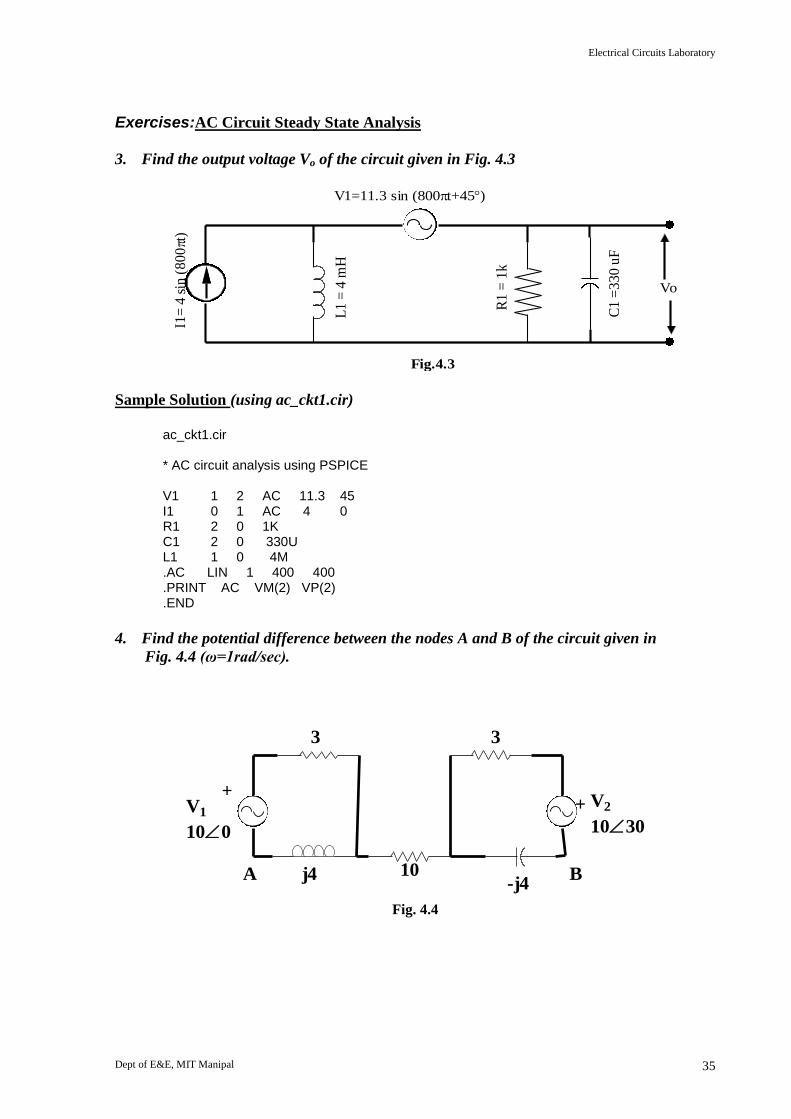
3. Find the output voltage Vo of the circuit given in Fig. 4.3
C1
=3
30 u
F
V1=11.3 sin (800t+45)
L1
= 4
mH
R1
= 1
k
Vo
Fig.4.3
I1=
4 s
in (
80
0t
)
Sample Solution (using ac_ckt1.cir)
ac_ckt1.cir * AC circuit analysis using PSPICE V1 1 2 AC 11.3 45 I1 0 1 AC 4 0 R1 2 0 1K C1 2 0 330U L1 1 0 4M .AC LIN 1 400 400 .PRINT AC VM(2) VP(2) .END
4. Find the potential difference between the nodes A and B of the circuit given in
Fig. 4.4 (ω=1rad/sec).
3 3
V1
100
V2
1030
j4 10-j4
A B
+
+
Fig. 4.4

Electrical Circuits Laboratory
Dept of E&E, MIT Manipal 36
Exercises:Three-phase AC Steady State Analysis
5. Find the neutral shift Von of the circuit given in Fig. 4.5 (ω=1rad/sec).
Fig. 6.5
220240
+
++
2200
220120
R1 = 10
R2 = 5 R3 = 6
XC = -j12 XL = j8
1
0
32
4
5 6
Fig. 4.5
Sample Solution (using ac_3ph1.cir) ac_3ph1.cir * Three phase AC analysis V1 1 0 AC 220 0 V2 2 0 AC 220 240 V3 3 0 AC 220 120 R1 1 4 10 R2 4 5 5 R3 4 6 6 L1 6 2 8 C1 5 3 0.08333 .AC LIN 1 0.159115 0.159115 .PRINT AC VM(4) VP(4) .END
6. A three phase, three wire, star connected 415V symmetrical ABC system supplies a
delta connected load where Zab = 5 , Zbc = 5 + j12 , Zca = 6 - j8 . Find the line
currents.
Exercises: Analysis of Coupled Circuits
7. Find the voltage across the capacitor in the circuit given in Fig. 4.6 (ω=1rad/sec)
Fig. 6.6
1001090
V1V2
++R1
5 5
R2
XC
-j10
XL1 = j5 XL2 = j5
XM = j2
Fig. 4.6

Electrical Circuits Laboratory
Dept of E&E, MIT Manipal 37
Sample Solution (using cup_ckt1.cir) cup_ckt1.cir * Analysis of coupled circuits using PSPICE V1 1 0 AC 10 0 V2 5 0 AC 10 90 R1 1 2 5 R2 4 5 5 L1 2 3 5 C1 3 0 0.1 L2 4 3 5 K1 L1 L2 0.4 .AC LIN 1 0.159115 0.159115 .PRINT AC VM(3) VP(3) .END
8. Find the current delivered by the source in the circuit given in Fig. 4.7 (ω=1rad/sec)
5
500
+
j8
Fig. 6.7
j3
2 4
M = j4
Fig. 4.7
Exercises:Analysis of Circuits with Controlled Sources
9. Find the output voltage Vo of the circuit given in Fig. 4.8 (ω=1rad/sec)
V1
120
V2
00
2Ix
C1
1F
C2
1F
Ix
R1 = 1 R2 = 1 L1 = 1H
Vo
+
+
R3
1
Fig. 4.8
Sample Solution (using ctl_ckt1.cir) ctl_ckt1.cir * Analysis of controlled circuits using PSPICE V1 1 0 AC 12 0 V2 5 0 AC 0 0 F1 0 3 V2 2 R1 1 2 1

Electrical Circuits Laboratory
Dept of E&E, MIT Manipal 38
R2 2 3 1 R3 4 0 1 C1 2 0 1 C2 4 5 1 L1 3 4 1 .AC LIN 1 0.159115 0.159115 .PRINT AC VM(4) VP(4) .END
10. Find the current Io of the circuit given in Fig. 4.9 (ω=1rad/sec)
-j1
0
0
1 1
1
j1
Io
Ia
+
+
2Ia
Fig. 4.9

Electrical Circuits Laboratory
Dept of E&E, MIT Manipal 39
TUTORIAL 5 Familiarization of PSPICE schematic
Invoke Pspice Capture Lite Edition OrCAD PSpice Capture Demo window appears.
A. Drawing the schematic
File New Project; Create a new project: Analog or Mixed A/D; Specify name of
project and location (user directory) – create blank project-Worksheet appears
i. Get all components and place them on the worksheet.
Place Part Part - R (analog.olb library) To change the resistance value double click on the value on the screen, type the value
required in value dialog box.
Get the source from source.olb library. The schematic should have GND as a reference node.
Place Ground (capsym). Change its name to 0
ii. Connect all components as in circuit diagram Place Wire
iii. Save the schematic in your directory.
B. Analysis
i. Pspice Create netlist
ii. PSpice New Simulation Profile-specify the name-click the type of analysis you want to
perform. Ex: click transient analysis for performing transient analysis, click AC sweep analysis for getting frequency response etc.
iii.Pspice Run
C. Results
To see the waveforms, place the voltage and current markers on the circuit. Trace Add Trace
Exercises: DC Transient Analysis
1. Observe the DC transients of the RLC series circuit of Fig. 5.1 for 10s in steps of 0.01
when the switch is closed at t=0 s.
+-10 V
R = 1 L = 1H
C =
10
mF
1
0
2 3
Fig. 7.1
Fig. 5.1
2. Repeat the above problem with resistance equal to (i) 20 and (ii) 100 for 10s in steps of
0.01s. Observe the differences.

Electrical Circuits Laboratory
Dept of E&E, MIT Manipal 40
3. Observe the various voltage and current transients of the circuit given in Fig. 5.2 for
2s in steps of 1ms. The switch is closed to position 1 at t=0 and it is changed to position
2 at t=0.5s.
10 V
R = 200
C =
1m
F
Fig. 7.2
a
b
1
0
2
10 V
Fig. 5.2
4. Observe the various voltages and current in the circuit given in Fig. 5.3.
R = 200C
= 1
mF
Fig.7.3
1
0
2
v(t)
-10
10per = 100 m
tw = 50 m
tr = tf = 1n
t
v(t)
IC =
10V
+
Fig. 5.3
Exercises: AC Transient Analysis
5. Observe two cycles of the AC transient response of the RL series circuit given in
Fig. 5.4. The switch is closed at = 60o.
+
Fig. 7.4
100
0.55
133
H
10si
n(1
00t
+60
0)
Fig. 5.4
Also observe the active, reactive, and apparent power associated with the above circuit.
Exercises: Frequency Response of Circuits
6. Observe the frequency response of the RLC series circuit of Fig. 5.5 as the frequency
is varied from 100Hz to 100kHz.Plot the frequency response of the current in the loop
and the voltage across the capacitor. From the current plot, find the resonant
frequency (fr), half power frequencies (fL, fU), and bandwidth (BW). Compare with the
theoretical values.

Electrical Circuits Laboratory
Dept of E&E, MIT Manipal 41
10 V
R = 2 L = 50H
C
10F
Fig. 10.5
f
+
Fig. 5.5
Observations
Trace the following waveform - I vs f ; Vc vs f, XL vs f ; XC vs f ; R vs f ; Z vs f ; impedance
angle vs f.
Mathematical Expressions for theoretical verification
For current response
i. Resonant frequency, fLC
r 1
2
ii. Q factor, QR
L
C
f L
R f RC
r
r
1 2 1
2
iii. Lower half-power frequency, f fQ QL r
1
2
1
21
2
iv. Upper half-power frequency, f fQ QU r
1
2
1
21
2
v. Bandwidth, BW f ff
QU L
r
2
7. Observe the frequency response of the circuit given in Fig.5.6 as the frequency is varied
from 300 to 3kHz. Plot the frequency response of the voltage across the capacitor and
find the resonant frequency, half power frequencies and bandwidth. Repeat for R=1
and R=6 and comment on the responses obtained.
1A
1mH
22F
Fig. 7.6
f
2
Fig 5.6
Observations
Trace the following waveform - V vs f ; BL vs f ; BC vs f ; G vs f ; Y vs f ; impedance angle
vs f.

Electrical Circuits Laboratory
Dept of E&E, MIT Manipal 42
Module III
Experiment No.1
SUPER POSITION & RECIPROCITY THEOREMS
OBJECTIVE:
To verify (a) super position theorem and (b) reciprocity theorems as applied to
electric circuits.
APPARATUS:
Sl. No. Apparatus Type Range Quantity
1 Standard resistors of different ranges - - 4
2 Milliammeters D.C. Suitable 2
3 Voltmeter D.C. 0 – 10V 1
4 T.P.S. Units D.C - 2
CIRCUIT DIAGRAM:
a) Superposition theorem:
(i) With both energy sources acting:
Fig. (i)
Current Source
0- 10v
R 1 = 100
R 2 = 100 R 3 = 50
R L = 25
TPS - 1
-
+
-
+
-
+
A
V
A
TPS - 2
Voltage Source

Electrical Circuits Laboratory
Dept of E&E, MIT Manipal 43
ii) With only current source acting:
Fig. i(a)
iii) With only the Voltage source acting:
Fig. i(b)
b) Reciprocity theorem:
Voltage excitation & Current response:
Fig. ii(a)
Voltage
source
Current
Source
RL
R3R2
R1
TPS - 1
-
+
-
+-
+
A
V
A
TPS - 2
R1
Voltage
Source
R3R2
RL=
-
+-
+
A
V
R2= _____ R3= _____
I1
-
+
A
R1= ___
R4= _____
TPS -
+
V

Electrical Circuits Laboratory
Dept of E&E, MIT Manipal 44
After exchanging the excitation and response
Fig. ii(b)
STATEMENTS:
a) Superposition theorem: It states that the response in any element of a linear, bilateral,
active network containing two or more energy sources is the sum of the responses
obtainable when each source is acting separately and all other energy sources set to
zero with their internal impedances, if any, remaining in the circuit.
b) Reciprocity theorem: It states that in a linear, bilateral, single source network, the
ratio of excitation to the response is constant, even when the positions of excitation
and response are interchanged.
PROCEDURE:
a) Superposition theorem:
1. Connect the circuit as shown in Fig. (i), after selecting suitable standard resistors
and milliammeter ranges.
2. Switch on both the voltage and current sources (TPS-1&2) and set them to
convenient values.
3. Note down the current through the load resistance RL and voltage across it.
4. Repeat the experiment for different voltage & current settings on the two energy
sources.
5. Rewire the circuit as shown in Fig. i(a).[ Here only the current source is acting in
the circuit and the voltage source is suppressed].
6. Switch on the current source, set it to previous fixed values and note down the
current through & voltage across the load resistance RL) each time.
7. Rewire the circuit as shown in Fig. i(b). [Here only the voltage source is acting in
the circuit and the current source is suppressed].
8. Switch on the voltage source, set it to previous fixed values and each time, note
down the current through and voltage across the load resistance RL.
0-10V
+
V
I2
R1
R2 R3
R4 TPS+
-
A
Electrical Circuits Laboratory
Dept of E&E, MIT Manipal 45
(b) Reciprocity theorem:
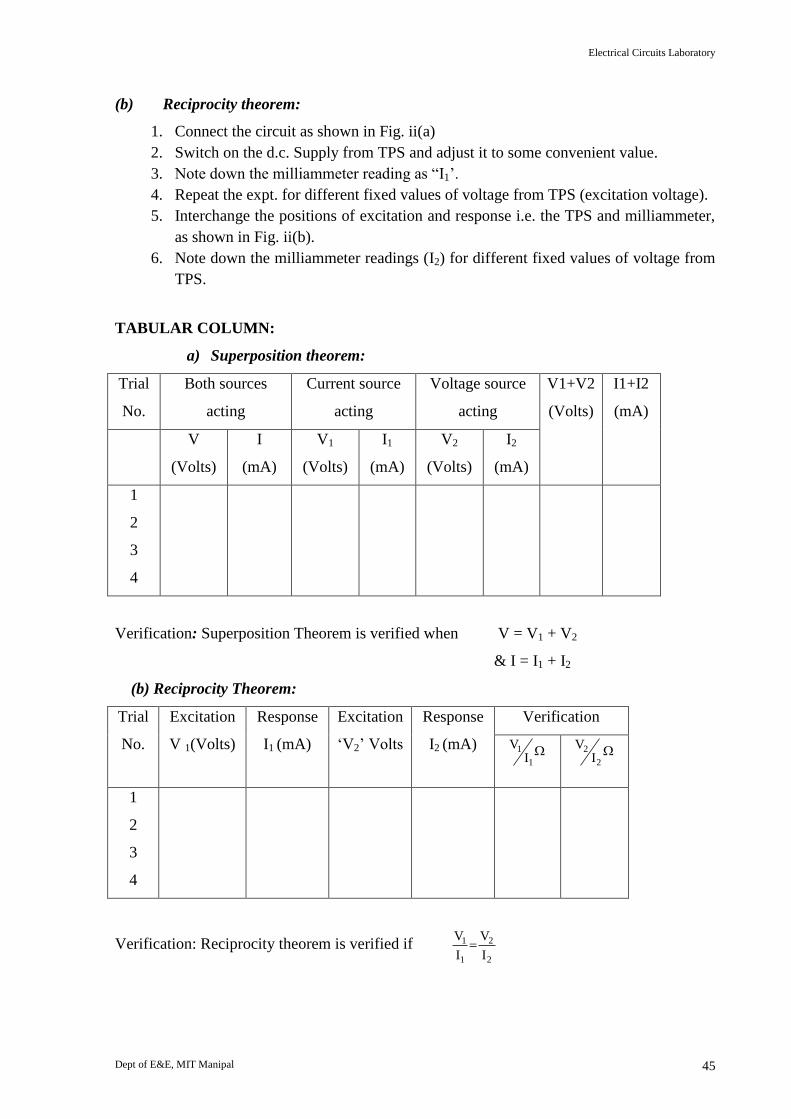
1. Connect the circuit as shown in Fig. ii(a)
2. Switch on the d.c. Supply from TPS and adjust it to some convenient value.
3. Note down the milliammeter reading as ―I1‘.
4. Repeat the expt. for different fixed values of voltage from TPS (excitation voltage).
5. Interchange the positions of excitation and response i.e. the TPS and milliammeter,
as shown in Fig. ii(b).
6. Note down the milliammeter readings (I2) for different fixed values of voltage from
TPS.
TABULAR COLUMN:
a) Superposition theorem:
Trial
No.
Both sources
acting
Current source
acting
Voltage source
acting
V1+V2
(Volts)
I1+I2
(mA)
V
(Volts)
I
(mA)
V1
(Volts)
I1
(mA)
V2
(Volts)
I2
(mA)
1
2
3
4
Verification: Superposition Theorem is verified when V = V1 + V2
& I = I1 + I2
(b) Reciprocity Theorem:
Trial
No.
Excitation
V 1(Volts)
Response
I1 (mA)
Excitation
‗V2‘ Volts
Response
I2 (mA)
Verification
1
1I
V 2
2I
V
1
2
3
4
Verification: Reciprocity theorem is verified if 2
2
1
1
I
V
I
V

Electrical Circuits Laboratory
Dept of E&E, MIT Manipal 46
CALCULATIONS:
Verify the practical results obtained, analytically by theoretical calculations.
SUPPLEMENTARY STUDY:
1. Can Superposition theorem be applied to determine the power consumed by an element?
Discuss.
2. Can Superposition and reciprocity theorems be applied to networks with dependent
sources? Discuss.
3. What are the applications of Superposition and Reciprocity theorems?
4. Verify the practical results obtained using PSPICE analysis.
-----------------------------------------------******-----------------------------------------------
Electrical Circuits Laboratory
Dept of E&E, MIT Manipal 47
R4=50 R3=25
R2=100 R1=50
TPS R5=10
B
A
RL=25
Experiment No.2
THEVENIN’S & NORTON’S THEOREMS
OBJECTIVE:
To verify (a) Thevenin‘s theorem and (b) Norton‘s theorem, as applied to electric
circuits.
APPARATUS:
Sl. No. Apparatus Type Range Quantity
1 Standard resistors - Suitable
ranges
5
2 Decade resistance box - 1
3 TPS Unit D.C - 1
4 Voltmeter D.C. 0 - 10V 2
5 Milliammeters D.C. Suitable
Ranges 2
CIRCUIT DIAGRAM:
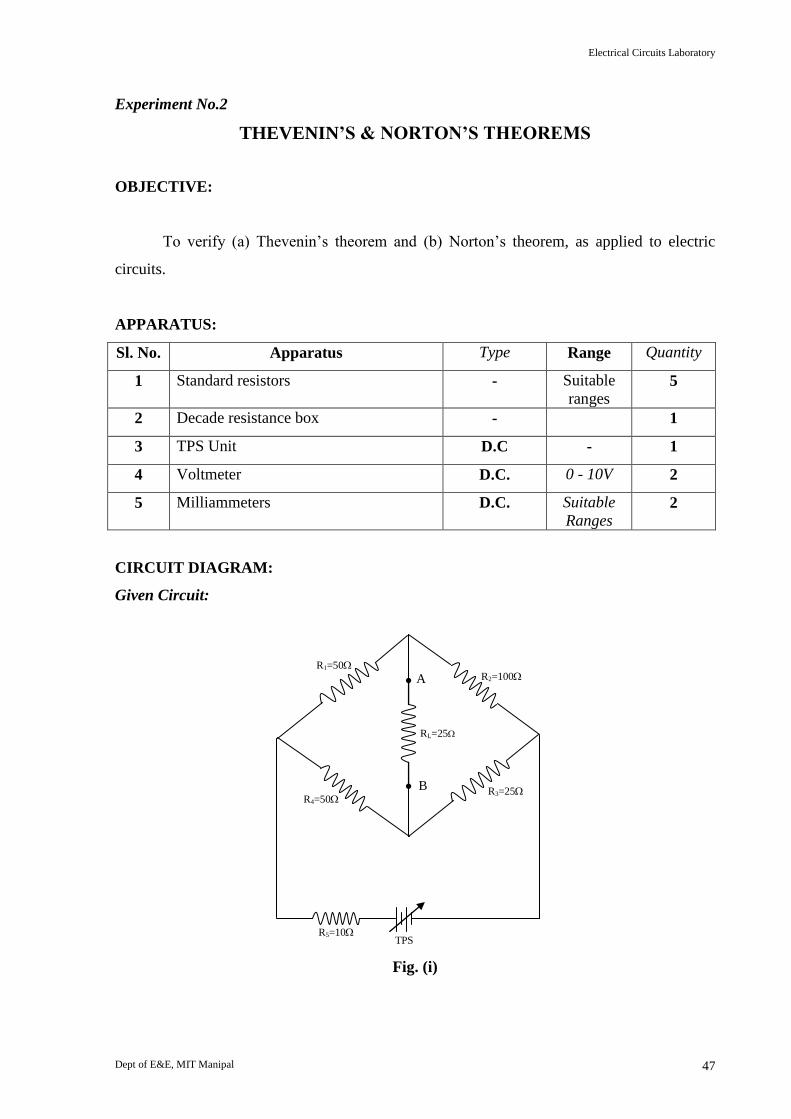
Given Circuit:
Fig. (i)

Electrical Circuits Laboratory
Dept of E&E, MIT Manipal 48
Verification of Thevenin’s theorem:
i. To find Load current in the Original circuit:
Fig. i(a)
ii. To find Open circuit Voltage ‘VTh:
Fig. i(b)
0-10V
R3 R4
RL
IL
B
TPS R5
+ A
R2 R1
A
+ V
R3 R4
TPS R5
B
R2 R1
VTh
-
+
V
0-10V
+ V
A

Electrical Circuits Laboratory
Dept of E&E, MIT Manipal 49
iii. To determine Thevenin’s equivalent resistance, ‘RTh’:
Fig. i(c)
iv. To find load current from Thevenin’s equivalent circuit:
Fig. i(d)
v. To find load current from Norton’s equivalent circuit:
RL
Rth
TPS - 1
-
+
-
+-
+
A
V
A
Isc
Fig. i(e)
+
-
V1
I1
R5
R3 R4
R2 R1
TPS
A1
B1
- +
0-10V V
A
RTh
IL1
RL
-
+
A
B
A A1 B
1
VTh
-
+
V
TPS

Electrical Circuits Laboratory
Dept of E&E, MIT Manipal 50
STATEMENTS:
a) Thevenin’s theorem:
In a linear bilateral active network containing many independent and controlled
sources, the current through the load can be obtained by replacing the entire network
by a single voltage source in series with an impedance, the voltage being equal to the
open circuit voltage across the load terminals, with the load removed and the
impedance is equal to the equivalent impedance of the network with respect to the
load terminals, with the load removed and with all the internal independent sources
set equal to zero.
b) Norton’s Theorem:
In a linear bilateral active network containing many independent and controlled
sources, the current through the load can be obtained by replacing the entire network
by a single current source in parallel with an impedance, the current being equal to
the short circuit current through the load terminals, with the load removed and the
impedance is equal to the equivalent impedance of the network with respect to the
load terminals, with the load removed and with all the internal independent sources
set equal to zero.
PROCEDURE:
a) Thevenin’s theorem:
1. Rig up the circuit as shown in Fig. i(a)., after selecting proper ranges for the meters.
2. Apply a convenient voltage from TPS and note down the load current ‗IL‘.
3. Repeat the above step for different fixed source voltage magnitudes.
4. Rig up the circuit as shown in Fig. i(b) & note down the value of open circuit voltage
VTH, across the terminals A&B for each fixed value of source voltage.
5. Rig up the circuit, as shown in Fig. i(c). Apply a reduced voltage from TPS and note
down the voltmeter and milliammeter readings. Calculate the value of Thevenin‘s
equivalent resistance.
6. Rewire the Thevenin‘s equivalent circuit, as shown in Fig. i(d). Note down the value
of load current IL1 for each value of VTh obtained from circuit in Fig. i(b).
b) Norton’s Theorem:
1. Rig up the circuit as shown in Fig. i(a)., after selecting proper ranges for the meters.
2. Apply a convenient voltage from TPS and note down the load current ‗IL‘.
3. Repeat the above step for different fixed source voltage magnitudes.
4. Rig up the circuit as shown in Fig. i(b) and replace the voltmeter connected across
terminals A & B by an ammeter.

Electrical Circuits Laboratory
Dept of E&E, MIT Manipal 51
5. Note down the value of short circuit current ISC, through the terminals A&B for each
fixed value of source voltage.
6. Rig up the circuit, as shown in Fig.i(c). Apply a reduced voltage from TPS and note
down the voltmeter and milliammeter readings. Calculate the value of Thevenin‘s
equivalent resistance.
7. Rewire the Norton‘s equivalent circuit, as shown in Fig. i(e). Note down the value of
load current IL1 for each value of ISC obtained from circuit in Fig. i(b).
TABULAR COLUMN:
(a) Thevenin’s Theorem:
Table (i) Table (ii)
Mean RTh =
Table (iii) Table (iv)
Trial
No.
Source voltage
‗V‘ in volts
‗IL‘ in mA
1
2
3
Trial
No.
‗V‘ in
volts
‗I‘ in
mA
RTh =
V/I in
Ohms
1
2
3
Trial
No.
Source voltage
‗V‘ in volts
VTh in volts
1
2
3
Trial
No.
‗VTh‘ in volts ‗IL1‘ in mA
1
2
3

Electrical Circuits Laboratory
Dept of E&E, MIT Manipal 52
Verification: Thevenin‘s theorem is verified if IL = IL1
(b) Norton’s Theorem:
Table (v) Table (vi)
Verification: Norton‘s theorem is verified if IL = IL1
Trial
No.
Source voltage
‗V‘ in volts
ISC in mA
1
2
3
Trial
No.
‗ISC‘ in volts ‗IL1‘ in mA
1
2
3

Electrical Circuits Laboratory
Dept of E&E, MIT Manipal 53
R4=50 R3=25
R2=100 R1=50
TPS R5=10
B
A
RL=25
Experiment No.3
MAXIMUM POWER TRANSFER THEOREM
OBJECTIVE:
To verify Maximum power transfer theorem, as applied to electric circuits.
APPARATUS:
Sl. No. Apparatus Type Range Quantity
1 Standard resistors - Suitable
ranges
5
2 Decade resistance box - 1
3 TPS Unit D.C - 1
4 Voltmeter D.C. 0 - 10V 1
5 Milliammeter D.C. Suitable
Ranges 1
CIRCUIT DIAGRAM:
Given Circuit:
Fig. (i)

Electrical Circuits Laboratory
Dept of E&E, MIT Manipal 54
Maximum power transfer theorem:
Fig. i(a)
STATEMENT:
It states that in any linear, active, bilateral network, maximum power is transferred
from the source to the load, when the load impedance becomes equal to the complex
conjugate of the Thevenin‘s impedance. As applied to D.C. circuits, it can be stated
that max. Power transfer takes place when the load resistance equals the Thevenin‘s
resistance (RTh) of the network.
PROCEDURE:
1. Connect the circuit, as shown in Fig. i(a).
2. Switch on the D.C. supply from TPS and keep it fixed at some convenient value.
3. Vary load resistance RL (decade resistance box) in steps, from minimum value and
note down the corresponding milliammeter and voltmeter readings.
4. Continue the variation of load resistance so that the readings are taken both before and
after the maximum power transfer.
5. Draw the graph of Power transferred verses load resistance.
R3 R4
RL
IL
B
TPS R5
+ A
R2 R1
-
A
+
V V

Electrical Circuits Laboratory
Dept of E&E, MIT Manipal 55
TABULAR COLUMN:
Trial
No.
V
(Volts)
IL in
(mA) L
LI
VR
()
LL RIP 2( )
(mW)

Electrical Circuits Laboratory
Dept of E&E, MIT Manipal 56
Verification:
From the graph, find out the value of load resistance RL corresponding to maximum power as
Rcr. At max. power transfer, this particular value of RL must be equal to equivalent internal
resistance of the network as viewed from the output terminals A&B, which is nothing but the
already calculated Thevenin‘s (or Norton‘s) equivalent resistance ‗RTH‘. Verify the same.
Also verify the practically determined max. power value with the theoretical value,
Pmax=Th
Th
R
V
4
2
= ___________ mW.
Load resistance, RL in
Specimen curve for Maximum power transfer theorem
SUPPLEMENTARY STUDY:
1. Verify the practical results obtained using PSPICE analysis.
2. What are the applications of Maximum Power Transfer theorem?
Rcr = RTh
Pmax
P in mW

Electrical Circuits Laboratory
Dept of E&E, MIT Manipal 57
Experiment No.4A
MEASUREMENT OF SELF & MUTUAL INDUCTANCE
OBJECTIVE:
To measure the self and mutual inductances of the given two inductive coils
APPARATUS:
Sl. No. Apparatus Type Range Quantity
1 Voltmeter D.C. 0 - 5V 1
2 Ammeter D.C. 0 – 500mA 1
3 Regulated power supply unit D.C - 1
4 Inductive coils - - 2
5 Autotransformer Single phase
- 1
6 Voltmeter A.C. 0 – 100V 1
7 Ammeter A.C. 0 – 1A 1
CIRCUIT DIAGRAM:
(i) To find d.c. resistances of the two coils :
Fig. (i)
+
0-5V
Coil
TPS
+
V
0-500mA
A

Electrical Circuits Laboratory
Dept of E&E, MIT Manipal 58
(ii) To find self inductances of the two coils :
Fig. (ii)
(iii) To find mutual inductance between the two coils :
a) Series Addition:
Fig. iii(a)
b) Series Opposition:
Fig. iii(b)
E
0 - 1A
N
P
C
B
A
0 - 100V
Coil
1Ph.
50Hz
230V
Supply
A
V
A
B Coil - 2
0–100V
Coil - 1
E
C
N
0-1A
4 3 2 1
1 Ph.
50Hz
230V
Supply
P
V
A
0 – 100V
0 - 1A
4 3 2 1
A
E
C
B
N
P
1 Ph.
50Hz
230V
Supply
V
Coil - 2
Coil - 1
A

Electrical Circuits Laboratory
Dept of E&E, MIT Manipal 59
PROCEDURE:
1) Connect the circuit as shown in Fig.(i).
2) Apply a low voltage d.c. and note down the d.c. meter readings to determine d.c.
resistance R1 of the first coil.
3) Repeat the steps (1) & (2) with the second coil to determine its d.c. resistance ‗R2‘
4) Rig up the circuit as shown in Fig. (ii) using coil-1.
5) Keeping the autotransformer in zero output position, switch on the a.c. supply.
6) Adjusting the autotransformer, apply a reduced voltage and note down the a.c. meter
readings to calculate the self-inductance L1 of the first coil.
7) Repeat the steps (5) & (6) with coil-2, to determine its self-inductance ‗L2‘.
8) Connect both the coils in series addition, as shown in Fig.iii(a). and repeat the steps (5)
& (6) to determine the reactance ‗m1‘. Care must be taken to see that the two coils are
co-axial by keeping them exactly one above the other.
9) Connect both the coils in series opposition, as shown in Fig. iii(b) and repeat the steps
(5) & (6) to determine the reactance ‗m2‘.
TABULATION & CALCULATIONS:
(i) To find D.C. resistances of the two coils
COIL - 1 COIL - 2
V1 Volts I1 Amp
1
11
I
VR
V2 Volts I2 Amp
2
22
I
VR

Electrical Circuits Laboratory
Dept of E&E, MIT Manipal 60
(ii) To find Self inductances of the two coils :
COIL – 1 COIL - 2
V1 (
Volt
s)
I 1 (
Am
p)
1
11
I
VZ
()
2
1
2
11 RZX L
()
f
XL L
2
11
(H)
V2 (
Volt
s)
I 2 (
Am
p)
2
22
I
VZ
()
2
2
2
22 RZX L
() f
XL L
2
22
(H)
(iii) To find mutual inductance between the two coils:
Series Addition Series Opposition
'
1V Volts '
1I Amps
'
1
'
1'
1I
VZ
'
2V Volts '
2I Amps
'
2
'
2'
2I
VZ
Here 2
21
2
21
'
1 )2()( MXXRRZ LL
2
21
2'
1 )()(221
RRZMXX LL = m1 = _________ ----------------(1)
Similarly, 22
21
1
2 )2()(21
MXXRRZ LL
2
21
2'
2 )()(221
RRZMXX LL = m2 = _________ ----------------(2)
Equations (1) – (2) gives, 4M = m1 m2
Mutual inductance ‗M‘ = 4
21 mm =
f
mm
8
21 = __________ H.
RESULTS:
1. Self inductance of coil-1 = ___________ H
2. Self inductance of coil-2 = ___________ H
3. Mutual inductance between the two coils = ___________ H
Electrical Circuits Laboratory
Dept of E&E, MIT Manipal 61
Experiment No.4B
POWER, POWER FACTOR & P.F. IMPROVEMENT
OBJECTIVE:
To measure the power consumed by fluorescent lamp, determine the operating power
factor, striking voltage, holding voltage and study the power factor improvement.
APPARATUS:
Sl. No. Apparatus Type Range Quantity
1 Fluorescent tube with choke and starter - - 1
2 Ammeter A.C. 0 – 1A 1
3 Voltmeter A.C. 0 – 300V 1
4 Wattmeter L.P.F. 1A/300V 1
5 Auto transformer Single phase 5A, 230V 1
6 Capacitor box - - 1
7 Switch S.P.S.T. - 1
8 Connecting wires - - -
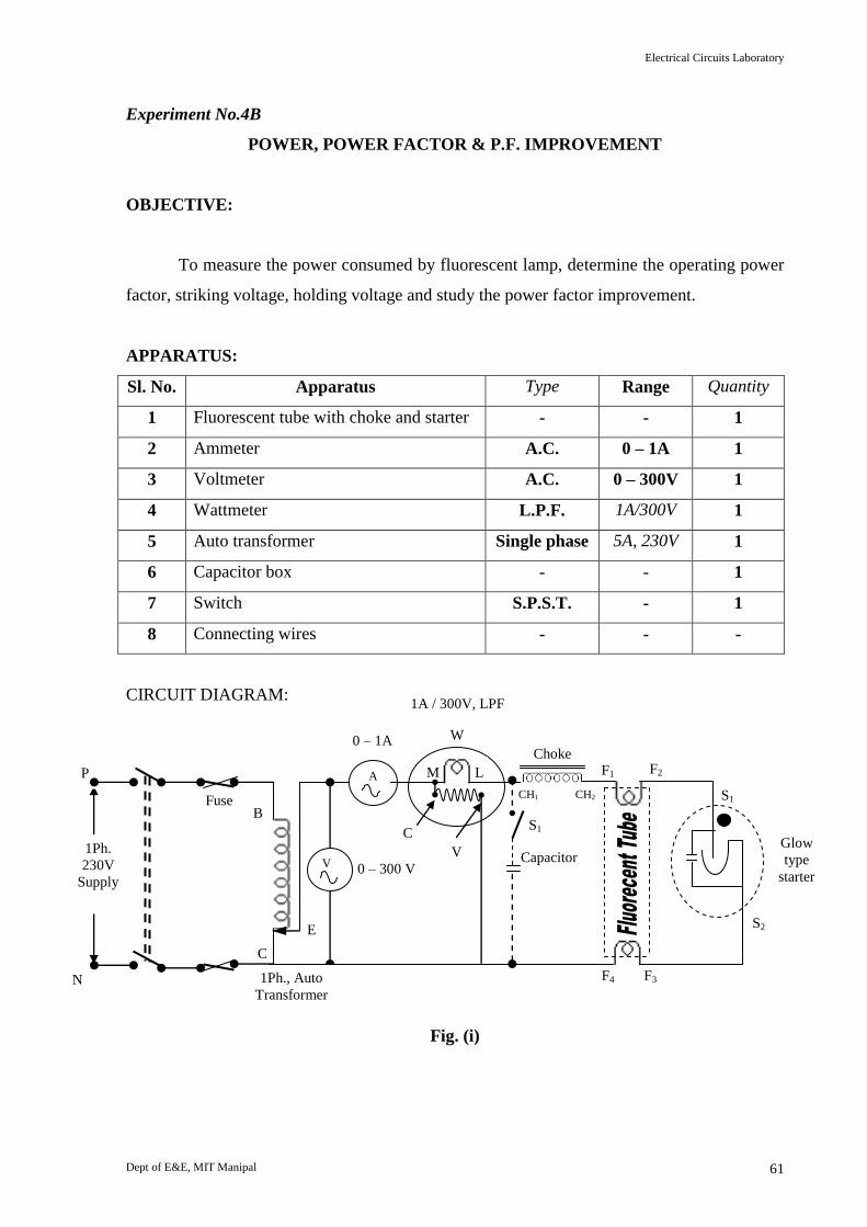
CIRCUIT DIAGRAM:
Fig. (i)
Capacitor
C
CH2 CH1
B
C
F3 F4
S2
S1
Glow
type
starter
F2 F1
E
W
1Ph., Auto
Transformer
Fuse
Choke
V
N
P A
1Ph.
230V
Supply
0 – 1A
0 – 300 V
1A / 300V, LPF
S1
M L
V

Electrical Circuits Laboratory
Dept of E&E, MIT Manipal 62
PROCEDURE:
1) Rig up the circuit as shown in the circuit diagram
2) Keeping the S.P.S.T. switch ‗S1‘ in open position and the autotransformer in zero output
position, switch on the supply.
3) Adjust the Autotransformer till the fluorescent lamp just strikes and note down the
striking voltage.
4) Increase the voltage up to rated value of 230V and note down all the meter readings.
5) Decrease the autotransformer voltage gradually till the fluorescent lamp goes off. Note
down the corresponding holding voltage.
6) Close the S.P.S.T. switch and take down all the meter readings at rated voltage.
7) Repeat the experiment for different values of capacitances.
8) Bring the autotransformer setting to zero output position and switch off the supply.
TABULAR COLUMN:
readingDeflectionScaleFull
FactorPowernCalibratioCCofRangeCoilessureofRange
Wattmeterthe
offactortionMultiplicai
..Pr)(
=
(ii) Striking Voltage = Volts.
(iii) Holding Voltage = Volts
Trail
No.
V
Volts
I
amps
W
Watts
Power factor
cos VI
W
Remarks
With out capacitor
With capacitor:
C1 = F

Electrical Circuits Laboratory
Dept of E&E, MIT Manipal 63
ANALYSIS OF POWER FACTOR IMPROVEMENT:
Referring to the power triangle shown below, let ‗P‘ be the active power consumed by the
lamp circuit at rated voltage V. Let cos1 be the original power factor and cos2 be the
improved p.f. Without the external capacitor, the lagging reactive power drawn by the circuit,
Q1= P tan1.
With the capacitor, the reactive power is reduced to
Q2= P tan 2
The leading reactive power of the capacitor is
given by
Q1 Q2= cX
V 2
where ‗Xc‘ is the capacitive reactance
Xc = 21
2
V
or
Capacitance ‗C‘ = cfX2
1Farads.
Thus, given the value to which the power factor is to be improved, the required capacitance
can be determined and compared with the practical values.
RESULTS:
(i) The power consumed by the fluorescent lamp at rated voltage = __________Watts
(ii) Corresponding power factor, ‗cos1‘ = _________
(iii) Improved power factor ―cos2‖ = _______ with C = _________ F.
(iv) Corresponding theoretical value of ‗C‘ = _________ F
SUPPLEMENTARY STUDY:
1. Discuss the other methods used for determination of self-inductance of a coil?
2. Discuss the causes of low power factor, disadvantages of low power factor and
methods of improving power factor.
-----------------------------------------------******-----------------------------------------------
2
S2
1 Q2
S1
P
(Q1 – Q2 )
Q1

Electrical Circuits Laboratory
Dept of E&E, MIT Manipal 64
Experiment No.5
THREE PHASE POWER MEASUREMENT
OBJECTVE:
To measure the active power in three phase star and delta connected circuits by Two
Wattmeter method.
APPARATUS:
Sl. No. Apparatus Type Range Quantity
1 Voltmeter A.C. 0 – 300V 1
2 Voltmeter A.C. 0 – 600V 2
3 Voltmeter A.C 0 - 100V 1
4 Ammeter A.C. 0 – 10A 4
5 Wattmeter U.P.F. 10A/600V 2
6 Resistive load 3 phase - -
CIRCUIT DIAGRAM:
(i) Star Connection :
Fig. (i)
O
0–600V
W1
0–10A
IB
IA
0–300V
VA V
B1
0–10A
10A/600V, UPF
IC
V C
L M
W2
V C
L M
10A/600V, UPF
3Ph., Star Connected
Load
C1
B2 C2
A2
A1 0–10A
VL
F
F
F
C
A
B
3Ph.
400V
50Hz
Supply
TPST
Mains
A
A
A
V
N

Electrical Circuits Laboratory
Dept of E&E, MIT Manipal 65
(ii) Delta Connection:
Fig. (ii)
PROCEDURE:
(i) Star connection:
1) Rig up the circuit as shown in Fig (i).
2) Keep the load switches off and switch on the three-phase supply.
3) Switch on the load in steps such that same current flows through all the ammeters
(balanced load) included in the three phases. Note down all the meter readings.
4) Now, switch on the load in such a way that unequal currents flow through the
ammeters connected in the three phases (unbalanced load). Note down all the meter
readings. Also note down the neutral shift voltage between the load star point ‗O‘
and supply neutral ‗N‘ (in case of 3 Ph., 3 wire, star connection only).
5) Switch off the load and then switch off the three phase mains.
(ii) Delta connection:
6) Rig up the Circuit as shown in Fig (ii).
7) Repeat the steps marked (2) to (5).
3Ph., Delta
Connected Load
0–10A
IC A
B2 B1 0–10A
IB
A
C2
C1
A2
A1
IA
0–10A
A
IL
0–10A
A
0–600V
V
F
F
F
C
A
B
3Ph.
400V
50Hz
Supply
TPST
Mains
V C
W1
L M
10A/600V, UPF
V C
L M
W2
10A/600V, UPF

Electrical Circuits Laboratory
Dept of E&E, MIT Manipal 66
TABULAR COLUMN:
Multiplication factor of wattmeter, wattmeterofreadingDSF
ncalibratiooffpCCofrangeCurrentCPofrangeVoltageW
...
......1
= _____________
Multiplication factor of wattmeter, W2 = ___________
Trial
No.
Star Connected Load (Assuming power factor of resistive load to be unity)
Line
Voltage
VL Volts
Phase voltages PhV.3
volts
Phase or line
currents
W1
watts
W2
watts
Total Power
W=(W1+W2)
watts
Total
power
consumed
W=(VAIA+
VBIB+
VCIC)
watts
Power factor, cos =
21
211 3tancos
WW
WW
VA
Volts
VB
Volts
VC
Volts
IA
Amp
IB
Amp
IC
Amp
Balanced Load
1
2
Unbalanced Load
1
2
Neutral
shift
voltage
(volts)

Electrical Circuits Laboratory
Dept of E&E, MIT Manipal 67
Trial
No.
Delta Connected Load (Assuming power factor of resistive load to be unity)
Line
Voltage
VL = phase
voltage, VPh =
VA=VB=VC
Volts
Line
Current
IL amp
Phase currents
PhI.3
amps
W1
watts
W2
watts
Total Power
W=(W1+W2)
watts
Total power
consumed
W=(VAIA+
VBIB+ VCIC)
watts
Power factor, cos
21
211 3tancos
WW
WW
IA
amps
IB
amps
IC
amps
Balanced load:
1
2
Unbalanced load:
1
2

Circuits Lab
Dept of E&E, MIT Manipal 1
RESULTS:
To be verified:
(i) For Star Connected balanced load, VL = PhV3
(ii) For Delta Connected balanced load, IL = PhI3
(iii) Star & Delta Connections – balanced & unbalanced loads,
(W1+W2) = (VAIA+VBIB+VCIC)
SUPPLEMENTARY STUDY:
1. Draw and explain the phasor diagrams for
a) Star connected, balanced, lagging p.f. load being supplied with
3 Ph., balanced, ABC sequence of supply.
b) Delta connected, balanced, U.P.F. load being supplied with 3 Ph.,
balanced, ABC sequence of supply.
2. While measuring three phase power by two wattmeter method, following
observations were made. Indicate the type of load and load power factor in
each case. Justify your answer.
i) One wattmeter reads negative and the other positive.
ii) Both meters read positive.
iii) Both the meters show same reading.
iv) One of the wattmeter shows zero reading.
v) One meter shows double the other.
-----------------------------------------------******--------------------------------------


