
D A T A S H E E T
M9421A VXT PXIe Vector Transceiver60 MHz to 3.8, or 6 GHz

Page 2Find us at www.keysight.com
Table of ContentsOverview ................................................................................................................................... 3Technical specifications ........................................................................................................... 4Vector signal analyzer performance ....................................................................................... 5Vector signal generator performance ................................................................................... 10General specifications ........................................................................................................... 14Front panel ............................................................................................................................. 14System requirements ............................................................................................................. 15Application specifications ..................................................................................................... 15N9063EM0D analog demodulation measurement application key specifications ............ 15N9069EM0D noise figure measurement application key specifications ............................ 16N9071EM0D GSM/EDGE/Evo measurement application key specifications .................... 18GSM/EDGE/Evo source key specifications .......................................................................... 19N9073EM0D W-CDMA/HSPA+ measurement application key specifications .................. 19W-CDMA/HSPA+ source key specifications ........................................................................ 20N9072EM0D cdma2000® measurement application and N9076EM0D 1xEV-DO measurement application key specifications ....................................................................... 22cdma2000 and 1xEV-DO source key specifications ............................................................ 22N9080EM0E LTE/LTE-Advanced FDD & N9082EM0E LTE/LTE-Advanced TDD measurement application key specifications ....................................................................... 22LTE source key specifications ............................................................................................... 23N9081EM0D Bluetooth® measurement application key specifications ............................. 23Bluetooth source key specifications ..................................................................................... 23N9079EM0D TD-SCDMA measurement application key specifications ............................ 24TD-SCDMA source key specifications .................................................................................. 24N9077EM0E and N9077EM1E WLAN measurement application key specifications ........ 25WLAN source key specifications........................................................................................... 26Software ................................................................................................................................. 27Related literature ................................................................................................................... 28Web ......................................................................................................................................... 28

Page 3Find us at www.keysight.com
M9421A VXT PXIe vector transceiver placed inside the M9018A PXIe chassis
Overview
Compress time, compress testThe best solution for a specific problem is a focused tool you simply fine-tune. Keysight’s M9421A PXIe vector transceiver (VXT) is purpose-built for rapid solution creation and faster throughput in manufacturing test of wireless components, power amplifiers, and RF front-end modules. With FPGA-accelerated measurements and deep software, the ready-to-run VXT lets you start closer to your finish line.
Product descriptionThe M9421A VXT is a four-slot PXIe vector signal generator and analyzer, ranging from 60 MHz to 3.8 or 6 GHz with modulation and analysis bandwidth up to 160 MHz. Up to four VXT’s can be configured in a single 18-slot PXI chassis, with only a single M9300A frequency reference required. Alternatively, a versatile single-chassis custom solution can be created from Keysight’s modular portfolio, dramatically reducing test footprint.
Applications – Power amplifier and front-end-module design validation
and manufacturing – Radio transceiver design validation and production test – Development, design validation, and manufacturing test for radios and other IoT
connected devices
Reference solutions Application-specific reference solutions, a combination of recommended hardware, soft-ware, and measurement expertise, provide the essential components of a test system. The following reference solutions include the M9421A PXIe VXT vector transceiver as a hardware component:
– RF power amplifier/front end module characterization and test, Reference Solution for the industry’s fastest power amplifier test solution including rapid waveform download, tight synchronization, automated calibration, and FPGA-accelerated power servo and fast power measurements. For more information, see www.keysight.com/find/solution-padvt

Page 4Find us at www.keysight.com
Technical Specifications
Definitions and conditions Specifications describe the warranted performance of calibrated instruments. Data represented in this document are specifications under the following conditions unless otherwise noted.
– Specifications are valid from 40 to 65 °C for individual module temperature, as reported by the module, and 20 to 35 °C for environment temperature unless otherwise noted
– Calibrated instrument has been stored for a minimum of 2 hours within the allowed operating range
– If instrument has previously been stored at a temperature range inside the allowed storage range, but outside the allowed operating range, instrument must have been stored for a minimum of 2 hours within the allowed operating range before turn-on
– 45-minute warm-up time – Calibration cycle maintained – An ALL Alignment has been run:
– Within the previous 3 days – If the temperature has changed more than 5 °C from the previous “ALL”
alignment
Typical describes additional product performance information that is not covered by the product warranty. It is performance beyond specifications that 95 percent of the units exhibit with a 95 percent confidence level. This data, shown in italics, does not include measurement uncertainty, and is valid only at room temperature (approximately 25 °C) after alignment within the stated alignment time and temperature limits.
Nominal values indicate expected performance, or describe product performance that is useful in the application of the product, but are not covered by the product warranty.
Recommended best practices in use – Use slot blockers and EMC filler panels in empty module slots to ensure proper
operating temperatures. Keysight chassis and slot blockers optimize module temperature performance and reliability of test.
– Set chassis fan to high at environmental temperatures above 45 °C.
Page 5Find us at www.keysight.com
Vector Signal Analyzer Performance
Performance
Capture depth
Standard 256 MSa of IQ data
Option M9421A-M05 512 MSa of IQ data
Frequency and Time Specifications
Frequency range
Option M9421A-504 60 MHz to 3.8 GHz
Option M9421A-506 60 MHz to 6 GHz
Frequency Reference
Accuracy, aging rate, stability refer to M9300A specifications
CW Measurement Frequency Accuracy
Accuracy (Transmitter frequency x frequency reference accuracy) ± 50 Hz typically
Resolution 1 Hz typical
Analysis Bandwidth
Maximum bandwidth Standard 60 to 70 MHz
70 to 80 MHz80 MHz to 6 GHz
10 MHz20 MHz40 MHz
Option M9421A-B85 60 to 70 MHz70 to 80 MHz80 to 230 MHz230 MHz to 6 GHz
10 MHz20 MHz40 MHz80 MHz
Option M9421A-B1X 60 to 70 MHz70 to 80 MHz80 to 230 MHz230 to 400 MHz400 MHz to 6 GHz
10 MHz20 MHz40 MHz80 MHz160 MHz
Triggering
Trigger IQ analyzer Free run, external 1, external 2, RF burst, video, periodic, PXI, internal
Trigger delay range –150 to 500 ms
Resolution 0.1 μs
Amplitude Accuracy and Range Specifications
Maximum average power input
RF input port +27 dBm
Option M9421A-HDX, Half duplex port +30 dBm

Page 6Find us at www.keysight.com
CW absolute amplitude accuracy
RF input port (in specified frequencies)
Frequency Range Input level ≤ –8 dBm to –70 dBm Input level > –8 dBm to +24 dBm
60 MHz to 230 MHz < ± 0.55 dB, < ± 0.20 dB typical < ± 0.65 dB, < ± 0.30 dB typical
230 MHz to 400 MHz 40 MHz BW 80 MHz BW
< ± 0.55 dB, < ± 0.20 dB typical< ± 0.65 dB, < ± 0.35 dB typical
< ± 0.55 dB, < ± 0.25 dB typical< ± 0.70 dB, < ± 0.30 dB typical
400 MHz to 510 MHz 40 MHz BW 80 MHz BW 160 MHz BW
< ± 0.50 dB, < ± 0.15 dB typical< ± 0.65 dB, < ± 0.35 dB typical< ± 0.60 dB, < ± 0.25 dB typical
< ± 0.55 dB, < ± 0.25 dB typical< ± 0.70 dB, < ± 0.30 dB typical< ± 0.70 dB, < ± 0.35 dB typical
510 MHz to 820 MHz 40 MHz BW 80 MHz BW 160 MHz BW
< ± 0.45 dB, < ± 0.20 dB typical< ± 0.55 dB, < ± 0.20 dB typical< ± 0.50 dB, < ± 0.20 dB typical
< ± 0.55 dB, < ± 0.30 dB typical< ± 0.50 dB, < ± 0.20 dB typical< ± 0.50 dB, < ± 0.20 dB typical
820 MHz to 1000 MHz 40 MHz BW 80 MHz BW 160 MHz BW
< ± 0.50 dB, < ± 0.20 dB typical< ± 0.45 dB, < ± 0.15 dB typical< ± 0.50 dB, < ± 0.15 dB typical
< ± 0.50 dB, < ± 0.30 dB typical< ± 0.50 dB, < ± 0.20 dB typical< ± 0.60 dB, < ± 0.25 dB typical
1000 MHz to 2110 MHz 40 MHz BW 80 MHz BW 160 MHz BW
< ± 0.50 dB, < ± 0.20 dB typical< ± 0.60 dB, < ± 0.25 dB typical< ± 0.60 dB, < ± 0.20 dB typical
< ± 0.65 dB, < ± 0.35 dB typical< ± 0.60 dB, < ± 0.20 dB typical< ± 0.60 dB, < ± 0.25 dB typical
2110 MHz to 3200 MHz 40 MHz BW 80 MHz BW 160 MHz BW
< ± 0.60 dB, < ± 0.25 dB typical< ± 0.65 dB, < ± 0.30 dB typical< ± 0.65 dB, < ± 0.30 dB typical
< ± 0.70 dB, < ± 0.35 dB typical< ± 0.60 dB, < ± 0.20 dB typical< ± 0.70 dB, < ± 0.30 dB typical
3200 MHz to 3310 MHz 40 MHz BW 80 MHz BW 160 MHz BW
< ± 0.65 dB, < ± 0.25 dB typical< ± 0.65 dB, < ± 0.30 dB typical< ± 0.70 dB, < ± 0.30 dB typical
< ± 0.70 dB, < ± 0.40 dB typical< ± 0.70 dB, < ± 0.25 dB typical< ± 0.85 dB, < ± 0.40 dB typical
3310 MHz to 3620 MHz 40 MHz BW 80 MHz BW 160 MHz BW
< ± 0.70 dB, < ± 0.35 dB typical< ± 0.70 dB, < ± 0.35 dB typical< ± 0.70 dB, < ± 0.35 dB typical
< ± 0.65 dB, < ± 0.35 dB typical< ± 0.65 dB, < ± 0.25 dB typical< ± 0.75 dB, < ± 0.40 dB typical
3620 MHz to 3900 MHz 40 MHz BW 80 MHz BW 160 MHz BW
< ± 0.65 dB, < ± 0.35 dB typical< ± 0.65 dB, < ± 0.45 dB typical< ± 0.70 dB, < ± 0.30 dB typical
< ± 0.70 dB, < ± 0.40 dB typical< ± 0.70 dB, < ± 0.30 dB typical< ± 0.85 dB, < ± 0.40 dB typical
3900 MHz to 4500 MHz 40 MHz BW 80 MHz BW 160 MHz BW
< ± 0.80 dB, < ± 0.40 dB typical< ± 0.80 dB, < ± 0.35 dB typical< ± 0.70 dB, < ± 0.35 dB typical
< ± 1.00 dB, < ± 0.55 dB typical< ± 0.80 dB, < ± 0.30 dB typical< ± 0.80 dB, < ± 0.35 dB typical
4500 MHz to 6000 MHz 40 MHz BW 80 MHz BW 160 MHz BW
< ± 0.90 dB, < ± 0.40 dB typical< ± 0.80 dB, < ± 0.35 dB typical< ± 0.80 dB, < ± 0.35 dB typical
< ± 1.00 dB, < ± 0.55 dB typical< ± 0.80 dB, < ± 0.35 dB typical< ± 0.80 dB, < ± 0.35 dB typical
Page 7Find us at www.keysight.com
Half duplex port, Option M9421A-HDX (in specified frequencies)
Frequency range Input level ≤ –8 dBm to –70 dBm Input level > –8 dBm to +24 dBm
60 MHz to 230 MHz < ± 0.50 dB, < ± 0.20 dB typical < ± 0.55 dB, < ± 0.25 dB typical
230 MHz to 400 MHz < ± 0.55 dB, < ± 0.25 dB typical < ± 0.60 dB, < ± 0.30 dB typical
400 MHz to 510 MHz 40 MHz BW 80 MHz BW 160 MHz BW
< ± 0.50 dB, < ± 0.20 dB typical< ± 0.50 dB, < ± 0.15 dB typical< ± 0.60 dB, < ± 0.25 dB typical
< ± 0.55 dB, < ± 0.25 dB typical< ± 0.60 dB, < ± 0.25 dB typical< ± 0.65 dB, < ± 0.30 dB typical
510 MHz to 820 MHz < ± 0.50 dB, < ± 0.20 dB typical < ± 0.55 dB, < ± 0.25 dB typical
820 MHz to 1000 MHz < ± 0.55 dB, < ± 0.25 dB typical < ± 0.55 dB, < ± 0.25 dB typical
1000 MHz to 2110MHz 40 MHz BW 80 MHz BW 160 MHz BW
< ± 0.60 dB, < ± 0.30 dB typical< ± 0.60 dB, < ± 0.25 dB typical< ± 0.60 dB, < ± 0.20 dB typical
< ± 0.60 dB, < ± 0.30 dB typical< ± 0.60 dB, < ± 0.30 dB typical< ± 0.65 dB, < ± 0.30 dB typical
2110 MHz to 3200 MHz 40 MHz BW 80 MHz BW 160 MHz BW
< ± 0.65 dB, < ± 0.30 dB typical< ± 0.65 dB, < ± 0.25 dB typical< ± 0.65 dB, < ± 0.30 dB typical
< ± 0.70 dB, < ± 0.40 dB typical< ± 0.70 dB, < ± 0.35 dB typical< ± 0.70 dB, < ± 0.35 dB typical
3200 MHz to 3310 MHz 40 MHz BW 80 MHz BW 160 MHz BW
< ± 0.60 dB, < ± 0.30 dB typical< ± 0.60 dB, < ± 0.20 dB typical< ± 0.60 dB, < ± 0.20 dB typical
< ± 0.65 dB, < ± 0.35 dB typical< ± 0.70 dB, < ± 0.35 dB typical< ± 0.70 dB, < ± 0.35 dB typical
3310 MHz to 3620 MHz 40 MHz BW 80 MHz BW 160 MHz BW
< ± 0.70 dB, < ± 0.35 dB typical< ± 0.70 dB, < ± 0.25 dB typical< ± 0.70 dB, < ± 0.30 dB typical
< ± 0.70 dB, < ± 0.35 dB typical< ± 0.70 dB, < ± 0.35 dB typical< ± 0.75 dB, < ± 0.40 dB typical
3620 MHz to 3900 MHz 40 MHz BW 80 MHz BW 160 MHz BW
< ± 0.70 dB, < ± 0.35 dB typical< ± 0.70 dB, < ± 0.30 dB typical< ± 0.85 dB, < ± 0.40 dB typical
< ± 0.75 dB, < ± 0.40 dB typical< ± 0.75 dB, < ± 0.40 dB typical< ± 0.75 dB, < ± 0.35 dB typical
3900 MHz to 4500 MHz < ± 0.85 dB, < ± 0.35 dB typical < ± 0.90 dB, < ± 0.50 dB typical
4500 MHz to 6000 MHz < ± 0.95 dB, < ± 0.5 dB typical < ± 1.00 dB, < ± 0.55 dB typical
Page 8Find us at www.keysight.com
Input voltage standing wave ratio (VSWR)
RF input port (in specified frequencies) 60 to 800 MHz 800 MHz to 1.3 GHz 1.3 to 3 GHz 3 to 4.2 GHz 4.2 to 6 GHz
< 2.0:1 nominal< 1.7:1 nominal< 1.5:1 nominal< 1.4:1 nominal< 1.9:1 nominal
Option M9421A-HDX, half duplex port (configured to input mode in specified frequencies)
60 MHz to 3 GHz 3 to 6 GHz
< 1.5:1 nominal< 1.7:1 nominal
Spurious responses (in specified frequencies)
Residual responses in specified frequency ranges
RF input port with analyzer range = 0 dBm 60 MHz to 230 MHz 230 MHz to 3.3 GHz 3.3 to 3.9 GHz 3.9 to 6 GHz
< –77 dBm typical< –90 dBm typical< –80 dBm typical< –87 dBm typical
Half duplex port with analyzer ranged to < –30 dBm 60 MHz to 6 GHz < –90 dBm typical
Other spurious, for offsets from 10 MHz up to half the maximum analysis bandwidth from the signal in specified frequency bands
< –62 dBc typical with analyzer ranged to signal peak power level
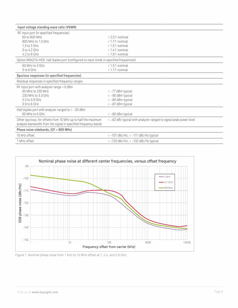
Phase noise sidebands, (CF = 900 MHz)
10 kHz offset < –107 dBc/Hz, < –111 dBc/Hz typical
1 MHz offset < –129 dBc/Hz, < –132 dBc/Hz typical
Figure 1. Nominal phase noise from 1 kHz to 10 MHz offset at 1, 2.4, and 5.8 GHz.

Page 9Find us at www.keysight.com
Displayed average noise floor (DANL)1
RF input port (in specified frequencies, with analyzer ranged to -70 dBm)
60 to 510 MHz 510 to 820 MHz 820 MHz to 1 GHz 1 to 2.11 GHz 2.11 to 3.2 GHz 3.2 to 3.31 GHz 3.31 to 3.62 GHz 3.62 to 3.9 GHz 3.9 to 4.5 GHz 4.5 to 6 GHz
–160 dBm, –164 dBm typical–159 dBm, –163 dBm typical–156 dBm, –160 dBm typical–154 dBm, –159 dBm typical–151 dBm, –156 dBm typical–156 dBm, –160 dBm typical–154 dBm, –158 dBm typical–153 dBm, –157 dBm typical–153 dBm, –158 dBm typical–150 dBm, –154 dBm typical
Half duplex port, option M9421A-HDX (in specified frequencies, with analyzer ranged to –70 dBm)
60 to 510 MHz 510 to 820 MHz 820 MHz to 1 GHz 1 to 2.11 GHz 2.11 to 3.2 GHz 3.2 to 3.31 GHz 3.31 to 3.62 GHz 3.62 to 4.5 GHz 4.5 to 6 GHz
–156 dBm, –161 dBm typical–155 dBm, –160 dBm typical–152 dBm, –157 dBm typical–150 dBm, –155 dBm typical–147 dBm, –152 dBm typical–152 dBm, –157 dBm typical–150 dBm, –154 dBm typical–149 dBm, –154 dBm typical–146 dBm, –151 dBm typical
Third-order intermodulation distortion (TOI)
60 MHz to 6 GHz +25 dBm nominal with analyzer ranged to 0 dBm+33 dBm nominal with analyzer ranged to +10 dBm
IF flatness
Center frequency (GHz) Span (MHz) Max. error (nominal)
≤ 6.0 ≤ 160 ± 0.30 dB
1. Input terminated, log power average, and normalized to 1 Hz bandwidth

Page 10Find us at www.keysight.com
Vector Signal Generator Performance
Performance
Arb baseband bandwidth
Standard M9421A-B40 60 to 70 MHz70 to 230 MHz230 MHz to 6 GHz
10 MHz20 MHz40 MHz
Option M9421A-B85 60 to 70 MHz70 to 230 MHz230 to 340 MHz340 MHz to 6 GHz
10 MHz20 MHz40 MHz80 MHz
Option M9421A-B1X 60 to 70 MHz70 to 230 MHz230 to 340 MHz340 to 400 MHz400 MHz to 6 GHz
10 MHz20 MHz40 MHz80 MHz160 MHz
Arb sample memory (storage capacity)
StandardOption M9421A-M05
256 MSa of IQ data512 MSa of IQ data
Frequency Specifications
Frequency range
Option M9421A-504Option M9421A-506
60 MHz to 3.8 GHz60 MHz to 6 GHz
Frequency reference
Accuracy, aging rate, stability Refer to M9300A specifications
Frequency Switching Speed1
Baseband frequency offset change2 ≤ 400 µs, nominal
Arbitrary frequency change3 ≤ 2 ms, nominal
1. Switching speed depends highly upon the hardware and controller that is used. Measurements were made with the M9421A in an M9018A chassis with the M9037A embedded controller.
2. Mean time from IVI command until baseband frequency changed from 0 to 1 kHz3. Mean time from IVI command until RF frequency changed from 1.8 to 1.0 GHz

Page 11Find us at www.keysight.com
Output Level Range
RF output port
60 MHz to 6 GHz –120 to +10 dBm
Option M9421A-HDX (configured to output mode)
60 MHz to 6 GHz –120 to +5 dBm ( –120 to +10 dBm CW typical)
Option M9421A-1EA
RF output port
60 MHz to 6 GHz –120 to +20 dBm (+25 dBm settable)
Option M9421A-HDX (configured to output mode)
60 MHz to 6 GHz –120 to +5 dBm (–120 to +15 dBm CW typical)
Amplitude Switching Speed1
Baseband power level change2 ≤ 400 μs, nominal
Arbitrary power level change3 ≤ 2 ms, nominal
1. Switching speed depends highly upon the hardware and controller that is used. Measurements were made with the M9421A in an M9018A chassis with the M9037A embedded controller.
2. Mean time from IVI command until baseband amplitude changed by 5 dB3. Mean time from IVI command until RF amplitude changed from 0 to -10 dBm

Page 12Find us at www.keysight.com
Absolute Level Accuracy (specified frequencies, CW)
RF output port
60 MHz to 380 MHz Level ≤ +20 dBm to –15 dBm Level ≤ –15 dBm to –80 dBm Level ≤ –80 dBm to –120 dBm
< ± 0.50 dB, < ± 0.15 dB typical< ± 0.55 dB, < ± 0.25 dB typical< ± 0.85 dB, < ± 0.50 dB typical
380 MHz to 1325 MHz Level ≤ +20 dBm to –15 dBm Level ≤ –15 dBm to –80 dBm Level ≤ –80 dBm to –120 dBm
< ± 0.50 dB, < ± 0.20 dB typical< ± 0.50 dB, < ± 0.20 dB typical< ± 0.85 dB, < ± 0.50 dB typical
1325 MHz to 2700 MHz Level ≤ +20 dBm to –15 dBm Level ≤ –15 dBm to –80 dBm Level ≤ –80 dBm to –120 dBm
< ± 0.50 dB, < ± 0.15 dB typical< ± 0.55 dB, < ± 0.25 dB typical< ± 0.90 dB, < ± 0.45 dB typical
2700 MHz to 3900 MHz Level ≤ +20 dBm to –15 dBm Level ≤ –15 dBm to –80 dBm Level ≤ –80 dBm to –110 dBm
< ± 0.70 dB, < ± 0.25 dB typical< ± 0.70 dB, < ± 0.30 dB typical< ± 1.10 dB, < ± 0.55 dB typical
3900 MHz to 6000 MHz Level ≤ +20 dBm to –15 dBm Level ≤ –15 dBm to –80 dBm Level ≤ –80 dBm to –100 dBm
< ± 0.65 dB, < ± 0.20 dB typical< ± 1.0 dB, < ± 0.50 dB typical< ± 1.10 dB, < ± 0.60 dB typical
Option M9421A-HDX, half duplex port
60 MHz to 380 MHz Level ≤ +5 dBm to –15 dBm Level ≤ –15 dBm to –80 dBm Level ≤ –80 dBm to –120 dBm
< ± 0.55 dB, < ± 0.20 dB typical< ± 0.50 dB, < ± 0.25 dB typical< ± 0.80 dB, < ± 0.40 dB typical
380 MHz to 1325 MHz Level ≤ +5 dBm to –15 dBm Level ≤ –15 dBm to –80 dBm Level ≤ –80 dBm to –120 dBm
< ± 0.55 dB, < ± 0.20 dB typical< ± 0.50 dB, < ± 0.20 dB typical< ± 0.85 dB, < ± 0.45 dB typical
1325 MHz to 2700 MHz Level ≤ +5 dBm to –15 dBm Level ≤ –15 dBm to –80 dBm Level ≤ –80 dBm to –120 dBm
< ± 0.55 dB, < ± 0.15 dB typical< ± 0.75 dB, < ± 0.35 dB typical< ± 0.95 dB, < ± 0.45 dB typical
2700 MHz to 3900 MHz Level ≤ +5 dBm to –15 dBm Level ≤ –15 dBm to –80 dBm Level ≤ –80 dBm to –110 dBm
< ± 0.65 dB, < ± 0.15 dB typical< ± 0.65 dB, < ± 0.30 dB typical< ± 1.10 dB, < ± 0.55 dB typical
3900 MHz to 6000 MHz Level ≤ +5 dBm to –15 dBm Level ≤ –15 dBm to –80 dBm Level ≤ –80 dBm to –100 dBm
< ± 0.70 dB, < ± 0.20 dB typical< ± 0.90 dB, < ± 0.45 dB typical< ± 1.10 dB, < ± 0.50 dB typical

Page 13Find us at www.keysight.com
Setting resolution
0.01 dB
Output voltage standing wave ratio (VSWR)
RF output port (in specified frequencies)
60 to 600 MHz 600 MHz to 2.8 GHz 2.8 to 5 GHz 5 to 6 GHz
< 1.6:1 nominal< 1.5:1 nominal< 1.5:1 nominal< 1.6:1 nominal
Option M9421A-HDX, half duplex port (configured to output mode in specified frequencies)
60 MHz to 2.9 GHz 2.9 to 6 GHz
< 1.4:1 nominal< 1.8:1 nominal
Harmonics and spurious
RF output port; harmonics and sub-harmonics
+10 dBm output power < –40 dBc nominal
Option M9421A-HDX, half duplex port; harmonics and sub-harmonics
+0 dBm output power < –40 dBc nominal
All ports; non-harmonic spurious (CW mode, specified frequency ranges)
60 MHz to 3.8 GHz 3.8 to 6 GHz
< –62 dBc nominal< –58 dBc nominal
Phase noise
Option M9421A-HDX, half duplex port, +5 dBm; RF output port, +15 dBm, CF = 900 MHz
10 kHz offset 100 kHz offset 1 MHz offset 10 MHz offset
≤ –106 dBc, –112 dBc typical≤ –109 dBc, –113 dBc typical≤ –128 dBc, –134 dBc typical≤ –131 dBc, –135 dBc typical
Broadband noise floor
RF output port Output level = +18 dBm Output level = –30 dBm
60 MHz to 3.5 GHz 3.5 to 5.5 GHz 5.5 to 6 GHz
–125 dBm, typical–120 dBm, typical–114 dBm, typical
–159 dBm, typical–161 dBm, typical–156 dBm, typical
Option M9421A-HDX, half duplex port Output level = +5 dBm Output level = –30 dBm
60 to 380 MHz 380 MHz to 5.5 GHz 5.5 to 6 GHz
–128 dBm, typical–130 dBm, typical–124 dBm, typical
–159 dBm, typical–160 dBm, typical–158 dBm, typical

Page 14Find us at www.keysight.com
General Specifications
Environmental Characteristics
Operating temperature +5 to +45 °C
Storage temperature –40 to +70 °C
EMC Complies with European EMC Directive 2004/108/EC – IEC/EN 61326-1 – CISPR Pub 11 Group 1, class A – AS/NZS CISPR 11 – ICES/NMB-001
This ISM device complies with Canadian ICES-001
Environmental stress Samples of this product have been type tested in accordance with the Keysight Environmental Test Manual and verified to be robust against the environmental stresses of storage, transportation, and end-use; those stresses include, but are not limited to, temperature, humidity, shock, vibration, altitude, and power line conditions; test methods are aligned with IEC 60068-2 and levels are similar to MILPRF-28800F Class 3.
Safety – Complies with European Low Voltage Directive 2006/95/EC – IEC/EN 61010-1 – Canada: CSA C22.2 No. 61010-1-04 – USA: UL Std. 61010-1
Power Requirement
Power drawn from chassis ≤ 120 W
Weight
NetShipping
1.6 kg (3.6 lbs)3.8 kg (8.4 lbs)
Dimensions
HeightWidthLength
130 mm (5.1 in)82 mm (3.2 in)209.5 mm (8.25 in)
Warranty
The VXT PXIe vector transceiver is supplied with a one-year warranty
Calibration Cycle
The recommended calibration cycle is two year; calibration services are available through Keysight service centers
Front Panel
Ref In
Connector SMB male, 50 Ω nominal
RF Connections
RF Input SMA female, 50 Ω nominal
RF Output SMA female, 50 Ω nominal
RFHD SMA female, 50 Ω nominal
Trigger Connections
Trigger In 1, Trigger In 2 Connector: SMB maleImpedance: 10 kΩ nominalTrigger level range: -3.5 to +3.5 V
Trigger Out 1, Trigger Out 2 Connector: SMB maleImpedance: 50 Ω nominalTrigger level range: 3.3 V LVTTL
Page 15Find us at www.keysight.com
System Requirements
Operating system Windows 7 (32 & 64 bit)
Processor speed 1.86 GHz minimum,2.4 GHz recommended
Available memory 4 GB minimum8 GB recommended
Available disk space 4 GB
Video Support for DirectX 9 graphics with 128 MB graphics recommended (SuperVGA supported)
Browser Microsoft Internet Explorer 7.0 or greater
Application Specifications
N9063EM0D analog demodulation measurement application key specifications1
Frequency Modulation2
FM Deviation Peak deviation5 ≥ 200 Hz to 400 kHz
FM Deviation Accuracy ± 0.5% × (rate + deviation) (nominal)
FM Rate 20 Hz to 50 kHz
FM Rate Accuracy ± 0.1 Hz (nominal)
Residual Distortion6 0.3% (nominal)
Amplitude Modulation3
AM Depth 1% to 99%
AM Depth Accuracy ± 0.2% + 0.002 × measured value (nominal)
AM Rate 50 Hz to 100 kHz
AM Rate Accuracy ± (0.01% × Reading) (nominal)
Residual Distortion6 0.25% (nominal)
Phase Modulation4
PM Deviation 0.2 to 100 rad
PM Deviation Accuracy ± (1 rad × (0.005 + (rate/1 MHz))) (nominal)
PM Rate 20 Hz to 50 kHz
PM Rate Accuracy ± 0.25 Hz (nominal)
Residual Distortion6 0.3% (nominal)
1. For specified frequency ranges between 60 and 3000 MHz, Channel BW ≤ 1 MHz.2. FM Rate: 400 Hz, 1 kHz, 10 kHz; FM Modulation Index: 1 to 20003. AM Rate: 400 Hz, 1 kHz, 10 kHz; AM Depth: 1% to 99%4. PM Rate: 400 Hz, 1 kHz, 10 kHz; PM Deviation: 1 to 100 rad5. Peak deviation, modulation index (“beta”), and modulation rate are related by Peak Deviation = Modulation Index × Rate.6. SINAD [dB] can be derived by 20 x log10 (1/Distortion), SINAD bandwidth: (Channel BW)/2.
Page 16Find us at www.keysight.com
Analog modulation source key specifications1
Frequency Modulation2
FM Deviation 200 Hz to 100 kHz
FM Deviation Accuracy ± 1% (nominal)
FM Rate 20 Hz to 40 kHz
FM Rate Accuracy Same as RF reference source, nominal
Residual Distortion5 1% (nominal)
Amplitude Modulation3
AM Depth 1% to 99%
AM Depth Accuracy ± 1% (nominal)
AM Rate 50 Hz to 40 kHz
AM Rate Accuracy Same as RF reference source, nominal
Residual Distortion5 0.25% (nominal)
Phase Modulation4
PM Deviation 0.2 to 20 rad
PM Deviation Accuracy ± 1% (nominal)
PM Rate 20 Hz to 40 kHz
PM Rate Accuracy Same as RF reference source, nominal
Residual Distortion5 0.5% (nominal)
1. For specified frequency ranges between 60 and 3000 MHz.2. FM Rate: 400 Hz, 1 kHz, 10 kHz; FM Modulation Index: 1 to 20003. AM Rate: 400 Hz, 1 kHz, 10 kHz; AM Depth: 5% to 95%4. PM Rate: 400 Hz, 1 kHz, 10 kHz; PM Deviation: 1 to 20 rad5. SINAD [dB] can be derived by 20 x log10 (1/Distortion).
N9069EM0D noise figure measurement application key specificationsThe specifications apply in the frequency range documented in the table 1. For the other frequency bands, external pre-selection filter is recommended.
Noise figure (60 MHz to 6 GHz)
Noise Source ENR Measurement Range Instrument Uncertainty
4 to 6.5 dB 0 to 20 dB ± 0.044 dB
12 to 17 dB 0 to 30 dB ± 0.095 dB
20 to 22 dB 0 to 35 dB ± 0.102 dB
Gain
Instrument uncertainty (DUT gain range = –20 to +40 dB)
60 MHz to 6 GHz ± 0.13 dB

Page 17Find us at www.keysight.com
Figure 2. Nominal instrument noise figure
Figure 3. Nominal instrument input VSWR
Nominal Instrument NF, 0.06 to 6 GHz, Range = –32 dBm
VSWR, Range = –32 dBm, 3 units
NF (dB)
GHz
17.5
15.5
13.5
11.5
9.5
7.5
5.50 1 2 3 4 5 6
GHz3 4 5 6210
2.2
1.8
1.6
1.4
1.2
1
2

Page 18Find us at www.keysight.com
N9071EM0D GSM/EDGE/Evo measurement application key specifications1
Power versus time (PvT)
Absolute power accuracy ± 0.36 dB nominal at 0 dBm input power
Phase error (GMSK modulation)
Phase error Average floor Peak floor
0.30º typical at 0 dBm input power0.85º typical at 0 dBm input power
EDGE error vector magnitude (EVM)
EVM RMS floor Peak floor
0.65% typical at 0 dBm input power2.0% typical at 0 dBm input power
Output RF spectrum (ORFS for GMSK and 8PSk modulation)
Residual relative power, spectrum due to modulation
Offset frequency 600 kHz 1.2 MHz 1.8 MHz
–70 dBc typical at 0 dBm input power–75 dBc typical at 0 dBm input power–73 dBc typical at 0 dBm input power
Residual relative power, spectrum due to switching
Offset frequency 600 kHz 1.2 MHz 1.8 MHz
–67 dBc typical at 0 dBm input power–74 dBc typical at 0 dBm input power–76 dBc typical at 0 dBm input power
1. For frequencies from 450 to 490 MHz, 820 to 920 MHz, and 1710 to 1910 MHz
Table 1. Frequency range for noise figure measurement
Frequency Band
60 MHz to 1000 MHz
1425 MHz to 1560 MHz
1620 MHz to 2030 MHz
2105 MHz to 2200 MHz
2300 MHz to 2700 MHz
3205 MHz to 3310 MHz
3400 MHz to 4300 MHz
4900 MHz to 5900 MHz

Page 19Find us at www.keysight.com
GSM/EDGE/Evo source key specifications1
Signal quality (RF output port: +15 dBm, Half duplex port: 0 dBm)
Phase error (GMSK)
RMS < 0.3° nominal
Peak < 2.0° nominal
EVM (EDGE)
RMS < 1% nominal
Output RF spectrum (ORFS)
Residual relative power, spectrum due to modulation
N9073EM0D W-CDMA/HSPA+ measurement application key specifications1
Channel power
Absolute power accuracy ± 0.36 dB nominal at 0 dBm input power
QPSK EVM
Residual EVM 0.85% typical at –10 dBm input power
Adjacent channel leakage ratio (ACLR) and adjacent channel power ratio (ACPR)
Residual relative power in 3.84 MHz BW 5 MHz offsets –65 dBc nominal at 0 dBm input power
Spectrum Emission Mask (SEM)
Residual relative power (offset)Downlink 2.515 to 2.715 MHz 2.715 to 3.515 MHz 3.515 to 4 MHz 4 to 8 MHz 8 to 12.5 MHz
–75 dBc in a 30 kHz BW typical at 0 dBm input power–77 dBc in a 1 MHz BW typical at 0 dBm input power–77 dBc in a 1 MHz BW typical at 0 dBm input power–67 dBc in a 1 MHz BW typical at 0 dBm input power–67 dBc in a 1 MHz BW typical at 0 dBm input power
Uplink 2.515 to 3.485 MHz 4 to 7.5 MHz 7.5 MHz to 8.5 MHz 8.5 to 12 MHz
–80 dBc in a 30 kHz BW typical at 0 dBm input power–65 dBc in a 1 MHz BW typical at 0 dBm input power–70 dBc in a 1 MHz BW typical at 0 dBm input power–70 dBc in a 1 MHz BW typical at 0 dBm input power
1. For frequencies from 695 MHz to 920 MHz and specified ranges from 1425 MHz to 2700 MHz
Offset GSM, nominalHalf duplext/RF output (0 dBm)
EDGE, nominalHalf duplext/RF output (0 dBm)
200 kHz400 kHz600 kHz1200 kHz1800 kHz
–35 dBc–68 dBc–76 dBc–81 dBc–77 dBc
–36 dBc–68 dBc–76 dBc–81 dBc–76 dBc
1. For frequencies from 380 to 490 MHz, 695 to 960 MHz, and 1425 to 2180 MHz
Page 20Find us at www.keysight.com
W-CDMA/HSPA+ source key specifications1
Signal quality (RF output port: +15 dBm, Half duplex port: 0 dBm)
Composite EVM
RMS < 1% nominal
Adjacent channel leakage ratio (ACLR)
Offset Port power levelconfiguration
Frequency (MHz) RF output/Half duplex0 dBm nominal (dB)
Adjacent 5 MHzAdjacent 10 MHzAdjacent 5 MHzAdjacent 10 MHzAdjacent 5 MHzAdjacent 10 MHzAdjacent 5 MHzAdjacent 10 MHz
1 DPCH 1 carrier
64 DPCH 1 carrier
900
1800 to 2200
900
1800 to 2200
–70–71–70–71–70–71–69–71
1. For frequencies from 695 MHz to 960 MHz, and 1425 MHz to 2180 MHz
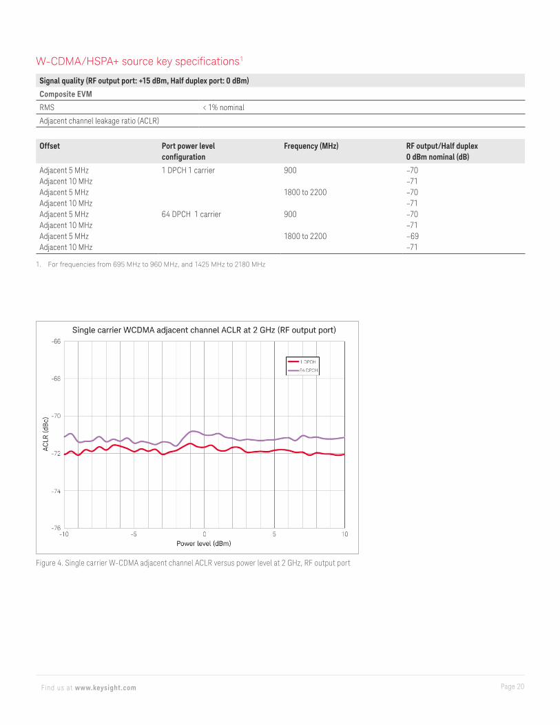
Figure 4. Single carrier W-CDMA adjacent channel ACLR versus power level at 2 GHz, RF output port
Page 21Find us at www.keysight.com
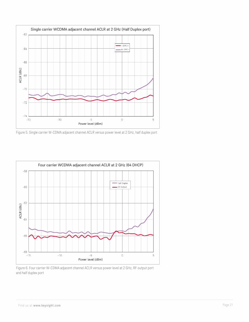
Figure 5. Single carrier W-CDMA adjacent channel ACLR versus power level at 2 GHz, half duplex port
Figure 6. Four carrier W-CDMA adjacent channel ACLR versus power level at 2 GHz, RF output port and half duplex port

Page 22Find us at www.keysight.com
N9072EM0D cdma2000 Measurement Application and N9076EM0D 1xEV-DO Measurement Application Key Specifications1
Channel power
Absolute power accuracy ± 0.36 dB nominal at 0 dBm input power
Error vector magnitude (EVM)
Residual EVM 0.85% typical at –10 dBm input power
Adjacent channel power (ACP)
Residual relative power in 30 kHz BW (offset) 750 kHz (DL), 885 kHz (UL) 1.98 MHz 4.0 MHz
–71 dBc typical at 0 dBm input power–83 dBc typical at 0 dBm input power–82 dBc typical at 0 dBm input power
1. For frequencies from 410 MHz to 484 MHz, 776 MHz to 920 MHz, and 1710 to 1980 MHz
cdma2000 and 1xEV-DO Source Key Specifications1
Signal quality (RF output port: +15 dBm, half duplex port: 0 dBm)
Composite EVM
RMS < 1.1% nominal
Adjacent channel power (ACP)
Residual relative power in 30 kHz BW (offset)
750 kHz (DL), 885 kHz (UL) –71 dBc nominal at 0 dBm input power
1.98 MHz –83 dBc nominal at 0 dBm input power
4.0 MHz –82 dBc nominal at 0 dBm input power
1. For frequencies from 380 MHz to 490 MHz, 695 MHz to 960 MHz, and 1425 MHz to 2180 MHz
N9080EM0E LTE/LTE-Advanced FDD & N9082EM0E LTE/LTE-Advanced TDD Measurement Application Key Specifications1
Transmit power
Absolute power accuracy ± 0.36 dB nominal at 0 dBm input power
Error vector magnitude (EVM)
Residual EVM
5 MHz, 10 MHz, 15 MHz, 20 MHz BW 0.8% typical at –10 dBm input power
Adjacent channel power
Minimum carrier power at RF input RF input port Half duplex port
–20 dBm–20 dBm
Dynamic range E-UTRA UTRA
Uplink, nominal –58 dBc–60 dBc
Downlink, nominal–56 dBc–58 dBc
1. For specified frequency ranges between 695 and 3800 MHz

Page 23Find us at www.keysight.com
N9081EM0D Bluetooth Measurement Application Key Specifications1
Transmit power
Absolute power accuracy ± 0.26 dB nominal at 0 dBm input power
Modulation characteristics
Deviation range ± 250 kHz nominal
EDR modulation accuracy
Range (rms DEVM) 0 to 12% nominal
Floor 0.6% typical at –20 dBm input power
1. Specifications apply for frequencies between 2400 and 2486 MHz.
Bluetooth Source Key Specifications1
Bluetooth signal using Signal Studio waveform
Basic Data Rate (ACL) FSK error at –10 dBm at half duplex port or RF output port 0.65% nominal, DH1 packet, GFSK, standard packet, 2402 MHz
Enhanced Data Rate ACP for –10 dBm signal at half duplex port or RF output port 3-DH1 packet, GFSK +D8PSK, standard packet, 2402 MHz
–69 dBm nominal, k=2; –72 dBm nominal, k= 3, 4, 5, …78
EDR rms DEVM error < 1% nominal
1. For specified frequency ranges between 1620 and 2700 MHz
LTE Source Key Specifications1
Signal quality (RF output port: +15 dBm, half duplex port: 0 dBm)
Composite EVM
RMS < 1.1% nominal
Adjacent channel power (ACP)
Adjacent, nominal Alternate, nominal
RF output/half duplex (0 dBm) RF output/half duplex (0 dBm)
900 MHz2 GHz
–64–65
–64–65
1. For specified frequency ranges between 695 and 3800 MHz
Page 24Find us at www.keysight.com
N9079EM0D TD-SCDMA Measurement Application Key Specifications1
Channel power
Absolute power accuracy ± 0.36 dB nominal at 0 dBm input power
Error vector magnitude (EVM)
Residual EVM, 1.6 MHz channel BW 0.75% typical at 0 dBm input power
Adjacent channel leakage ratio (ACLR) and adjacent channel power ratio (ACPR)
Residual relative power in 1.28 MHz BW 1.6 MHz offset 3.2 MHz offset
–55 dBc typical at 0 dBm input power–70 dBc typical at 0 dBm input power
Spectrum emission mask (SEM)
Residual relative power (offset)Downlink 815 kHz to 1.015 MHz 1.015 to 1.815 MHz 1.815 to 2.3 MHz 2.3 to 4 MHz
–60 dBc in a 30 kHz BW nominal at 0 dBm input power–68 dBc in a 1 MHz BW nominal at 0 dBm input power–71 dBc in a 1 MHz BW nominal at 0 dBm input power–58 dBc in a 1 MHz BW nominal at 0 dBm input power
Uplink 815 kHz to 1.8 MHz 1.8 to 2.385 MHz 2.9 to 3.5 MHz
–54 dBc in a 30 kHz BW typical at 0 dBm input power–68 dBc in a 1 MHz BW typical at 0 dBm input power–71 dBc in a 1 MHz BW typical at 0 dBm input power
1. For specified frequency ranges between 1620 and 2700 MHz
TD-SCDMA Source Key Specifications1
Signal quality (RF output port: +15 dBm, half duplex port: 0 dBm, full duplex port: –20 dBm)
Composite EVM
RMS < 0.5% nominal
Adjacent channel power (ACP)
Residual relative power in 30 kHz BW 1.6 MHz offset 3.2 MHz offset
–65 dBc nominal at 0 dBm input power–68 dBc nominal at 0 dBm input power
1. For specified frequency ranges between 1620 and 2700 MHz

Page 25Find us at www.keysight.com
Figure 7. 802.11 a/g SEM nominal performance at 2.4 GHz with 20 MHz BW
Figure 8. 802.11 a/g SEM nominal performance at 5.8 GHz with 20 MHz BW
Figure 9. 802.11 n SEM nominal performance at 5.8 GHz with 40 MHz BW
Figure 10. 802.11 ac SEM nominal performance at 5.8 GHz with 80 MHz BW
N9077EM0E and N9077EM1E WLAN Measurement Application Key Specifications1
Modulated Power
Absolute power accuracy 2400 MHz to 2483.5 MHz 5150 MHz to 5185 MHz
± 0.27 dB nominal at 0 dBm input power± 0.49 dB nominal at 0 dBm input power
Error Vector Magnitude (EVM)
EVM floor conditions Phase Tracking on, pre-amble only, Half duplex port
802.11b 2.4 GHz < –40.9 dB typical at –20 dBm input power
802.11g 2.4 GHz < –47 dB typical at –20 dBm input power
802.11a 5.8 GHz < –48 dB typical at –20 dBm input power
802.11n 5.8 GHz 20 MHz802.11n 5.8 GHz 40 MHz
< –48 dB typical at –20 dBm input power< –44 dB typical at –20 dBm input power
802.11ac 5.8 GHz 80 MHz802.11ac 5.8 GHz 80 MHz802.11ac 5.8 GHz 160 MHz
< –45 dB typical at –20 dBm input power< –48 dB nominal at –5 dBm input power< –43 dB typical at –20 dBm input power
802.11ax 5.8 GHz 80 MHz < –49 dB nominal at -10 dBm input power
SEM
802.11a/g at 2. 4GHz with 20 MHz BW See Figure 5
802.11a/g at 5.8 GHz with 20 MHz BW See Figure 6
802.11n at 5.8 GHz with 40 MHz BW See Figure 7
802.11ac at 5.8 GHz with 80 MHz BW See Figure 8
1. SEM Transmitter test signal generated by Agilent N5182B MXG signal generator

Page 26Find us at www.keysight.com
Figure 11. 802.11 ac EVM nominal performance versus power level at 5.8 GHz for 160 MHz signal bandwidth with equalization on the preamble
WLAN Source Key Specifications
Error Vector Magnitude (EVM)
Wireless LAN error vector magnitude (EVM Performance (using Signal Studio signal noted)) half duplex port, RF output port
802.11b 2.4GHz < –28 dB typical (0 dBm to –30 dBm)
802.11a 5.8 GHz < –44 dB typical (–5 dBm to –15 dBm)
802.11n 5.8 GHz 20MHz802.11n 5.8 GHz 40MHz
< –43 dB typical (–5 dBm to –15 dBm)< –44 dB typical (–5 dBm to –15 dBm)
802.11ac 5.57GHz 80MHz802.11ac 5.8 GHz 80 MHz802.11ac 5.57GHz 160MHz
< –47 dB typical (–5 dBm to –15 dBm)< –49 dB nominal (–5 dBm)< –45 dB typical (–5 dBm to –15 dBm)
802.11ax 5.8 GHz 80 MHz < –50 dB nominal (–10 dBm)

Page 27Find us at www.keysight.com
Software
Instrument connection software
Keysight I/O library The I/O library suite offers a single entry point for connection to the most common instruments including AXIe, PXI, GPIB, USB, Ethernet/LAN, RS-232, and VXI test instruments from Keysight and other vendors. It automatically discovers interfaces, chassis, and instruments. The graphi-cal user interface allows you to search for, verify, and update IVI instrument and soft front panel drivers for modular and traditional instruments. The IO suite safely installs in side-by-side mode with NI I/O software.
Free software download atwww.keysight.com/find/iosuite
Module setup and usage
Keysight soft front panel The VXT includes a soft front panel (SFP), a software-based graphical user interface (GUI) which enables the instrument’s capabilities from your PC.
Included on CD-ROM shipped with module or online
Module management
Keysight connection expert Connection expert is the graphical user interface included in the I/O libraries suite that allows you to search for, verify and update IVI instrument and soft front panel drivers for modular and traditional instruments
Free software download atwww.keysight.com/find/iosuite
Programming
DriverIVI-COMIVI-CMATLAB
Development environmentsVisual Studio (VB .NET, C#, C/C++), VEE, LabVIEW, LabWindows/CVI, MATLAB
Included on CD-ROM shipped with module or online
Programming assistance
Command expert Assists in finding the right instrument commands and setting correct parameters. A simple interface includes documentation, examples, syntax checking, command execution, and debug tools to build sequences for integration in Excel, MATLAB, Visual Studio, and VEE.
Free software download atwww.keysight.com/find/commandexpert
Signal analysis software
X-Series measurement applications Provides measurements for analog demodulation, noise figure, phase noise and others.
Licensed software. For more information, visit www.keysight.com/find/x-series_apps

This information is subject to change without notice. © Keysight Technologies, 2019, Published in USA, June 7, 2019, 5992-1646EN
Page 28Find us at www.keysight.com
Learn more at: For more information on Keysight Technologies’ products, applications or services,
please contact your local Keysight office. The complete list is available at:
www.keysight.com/find/contactus
Related Literature
Literature Pub number
M9421A VXT PXIe Vector Transceiver - Configuration Guide 5992-1641EN
M9018A PXIe 18 slot Chassis - Data Sheet 5990-6583EN
M9037A PXIe High Performance Embedded Controller - Data Sheet 5991-3661EN
M9036A PXIe Embedded Controller - Data Sheet 5990-8465EN
Web
Product page: www.keysight.com/find/M9421A X-Series measurement applications: www.keysight.com/find/X-Series_Apps
For more information or literature resources please visit the web:www.keysight.com/find/vxt
cdma2000 is a US registered certification mark of the Telecommunications Industry Association.
Bluetooth and the Bluetooth logos are trademarks owned by Bluetooth SIG, Inc., U.S.A. and licensed to Keysight Technologies, Inc.


