
Linköping University Post Print
Low-Temperature Superionic Conductivity in
Strained Yttria-Stabilized Zirconia
Michael Sillassen, Per Eklund, Nini Pryds, Erik Johnson, Ulf Helmersson and Jorgen Bottiger
N.B.: When citing this work, cite the original article.
Original Publication:
Michael Sillassen, Per Eklund, Nini Pryds, Erik Johnson, Ulf Helmersson and Jorgen
Bottiger, Low-Temperature Superionic Conductivity in Strained Yttria-Stabilized Zirconia,
2010, ADVANCED FUNCTIONAL MATERIALS, (20), 13, 2071-2076.
http://dx.doi.org/10.1002/adfm.201000071
Copyright: John Wiley & Sons, Ltd
http://eu.wiley.com/WileyCDA/Brand/id-35.html
Postprint available at: Linköping University Electronic Press
http://urn.kb.se/resolve?urn=urn:nbn:se:liu:diva-58538
1 1
Low temperature superionic conductivity in strained yttria-
stabilized zirconia
Michael Sillassen*, Per Eklund, Nini Pryds, Erik Johnson, Ulf Helmersson, and Jørgen
Bøttiger*
[*] M. Sillassen, Prof. J. Bøttiger
Interdisciplinary Nanoscience Center (iNANO) and Department of Physics and Astronomy,
University of Aarhus, DK-8000 Aarhus C, Denmark
E-mail: [email protected], [email protected]
Dr. P. Eklund, Prof. U. Helmersson
Department of Physics, Chemistry, and Biology, IFM,
Linköping University, SE-581 83 Linköping, Sweden
Dr. N. Pryds, Dr. E. Johnson
Risø National Laboratory for Sustainable Energy Technical University of Denmark - DTU,
DK-4000 Roskilde, Denmark
Keywords: YSZ, solid electrolytes, epitaxy, interfaces, sputtering
Abstract
We report very high lateral ionic conductivities in epitaxial cubic yttria-stabilized zirconia
synthesized on single crystal SrTiO3 and MgO substrates by reactive direct current magnetron
sputtering. Superionic conductivities (i.e., ionic conductivities of the order ~1 Ω-1
cm-1
) are
observed at 500 ºC for 58-nm-thick films on MgO. Our results indicate a superposition of two
parallel contributions – one due to bulk and one attributable to the film-substrate interface.
Interfacial effects dominate the conductivity at low temperatures (<350 oC), showing more
than three orders of magnitude enhancement compared to bulk YSZ. At higher temperatures,
a more bulk-like conductivity is observed. The films have a negligible grain-boundary
network, thus ruling out grain boundaries as a pathway for ionic conduction. The observed
enhancement in lateral ionic conductivity is caused by a combination of misfit dislocation
density and elastic strain in the interface. These very high ionic conductivities in the
temperature range 150 – 500 ºC are of great fundamental importance but may also be
technologically relevant for low-temperature applications.

2 2
1. Introduction
The field of nanoionics studies nanoscale and interfacial effects on ionic conductors. A
number of studies have indicated that the migration of ions in nanocrystalline materials is
mainly affected by grain boundaries and interfaces,[1-4]
which can exhibit orders of magnitude
greater diffusivity than that of the lattice.[5,6]
In simplified model systems such as
superlattices,[7-9]
or highly textured thin films,[10,11]
these effects have been demonstrated. Of
particular interest to the present work is the cubic yttria-stabilized zirconia (YSZ) system due
to the large-scale application potential as electrolytes in solid oxide fuel cells (SOFCs).[12-14]
We have previously demonstrated a mixed bulk- and grain-boundary conduction mechanism
in sputtered nanocrystalline (nc) YSZ films,[15]
reporting increasing ionic conductivity with
decreasing grain size. However, in order to benefit from nanoionic effects in practical SOFCs,
these effects need to be demonstrated at low temperatures, since a key step towards improving
the technology is the reduction of the operating temperature, which is currently above 600 ºC.
Relevant literature only presents few cases in which the origin of the enhanced
diffusion at grain boundaries and interfaces has been well established, and usually these
studies have been carried out at elevated temperatures.[16]
In the present study, we search for
interfacial effects at lower temperatures in the simplest model system possible, i.e., epitaxial
YSZ films devoid of grain boundaries fabricated on various single crystals with different
orientation and lattice mismatch. In this way, we are able to separate contributions associated
with grain boundaries, interfaces, and bulk (lattice) processes.
In the present paper, we report the enhancement in lateral ionic conductivity of up to
3.5 orders of magnitude as compared to bulk YSZ at temperatures as low as 150 ºC due to
interfacial effects. At temperatures above 350 ºC, a more bulk-like conductivity is observed
for all samples. Superionic conductivities (~1 Ω-1
cm-1
) are ultimately obtained for 58-nm-
thick YSZ films on MgO at a temperature of 500 ºC. These very high ionic conductivities in
the temperature range 150 – 500 ºC are of great fundamental importance but may also be
3 3
technologically relevant especially for unconventional low-temperature micro-SOFC
applications.
2. Results and Discussion
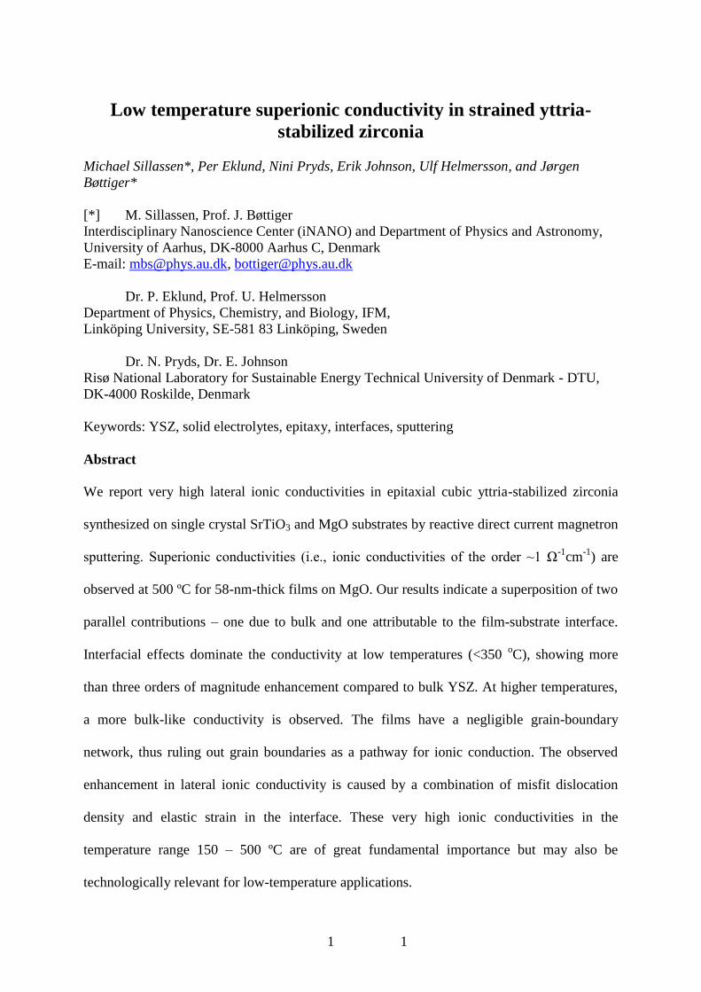
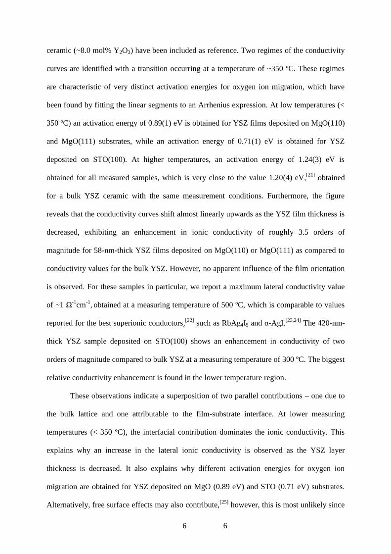
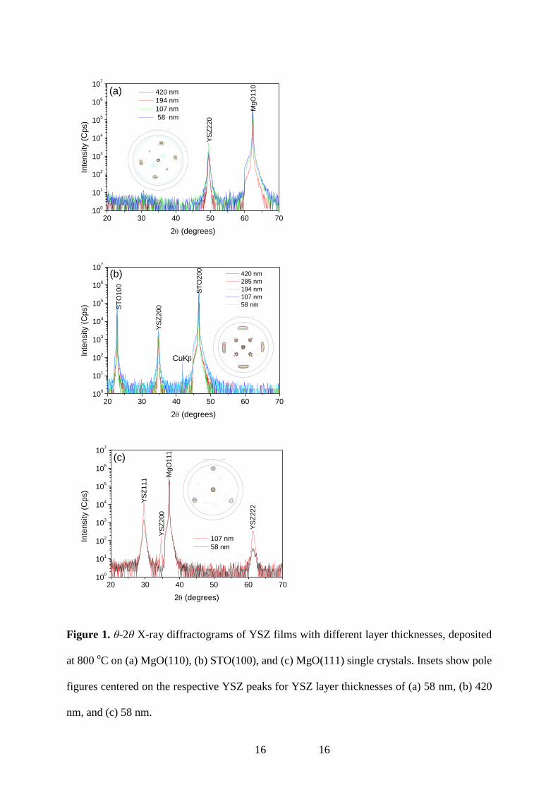
Fig. 1(a), 1(b), and 1(c) show θ-2θ X-ray diffractograms of YSZ films with different
thicknesses deposited on MgO(110), STO(100), and MgO(111), respectively, with a substrate
temperature of 800 oC. For depositions made on MgO, the observed peaks, corresponding to
cubic YSZ, are shifted towards larger d-values in the out-of-plane direction, compared to
powder diffractograms.[17]
This shift corresponds to in-plane elastic (compressive) strain of
the order -1%. For depositions made on (a) MgO(110) and (b) STO(100), the θ-2θ scans
reveal a high degree of out-of-plane alignment of the cubic YSZ films to the respective
substrates, regardless of layer thickness. In Fig. 1(c), alignment to the MgO(111) substrate is
only observed at a YSZ layer thickness of 58 nm.
The inset in Fig. 1(a) shows a pole-figure plot of the YSZ 220 peak for an YSZ layer
thickness of 58 nm, identical to the pole figure (not shown) of the bare MgO(110) substrate,
thus confirming epitaxial growth of the YSZ(220) film on MgO(110). A predominant 220
peak can be seen at zero χ, with four additional peaks at χ = 60o due to the fourfold symmetry
of {110} planes. The two peaks at χ = 45o originate from the MgO 200 peak. The full epitaxy
is lost at a layer thickness of 420 nm, where small contributions from the YSZ 311 peak are
observed (pole figure not shown). The inset in Fig. 1(b) shows a pole figure centered on the
YSZ 200 peak for a layer thickness of 420 nm deposited on STO(100). A predominant 200
peak is observed at zero χ. All other peaks are identified as belonging to the substrate. The
four peaks at χ = 45o originate from the STO 110 peak. The four peaks at χ ≈ 35.3º and the
eight peaks (four double peaks) at χ ≈ 65.9º originate from the STO 211 peak. In the inset of
Fig. 1(c), the pole-figure plot of the YSZ 111 peak is shown for a layer thickness of 58 nm. A
4 4
predominant 111 peak is observed at zero χ, with three additional peaks at χ ≈ 70.5o due to the
threefold symmetry of {111} planes.
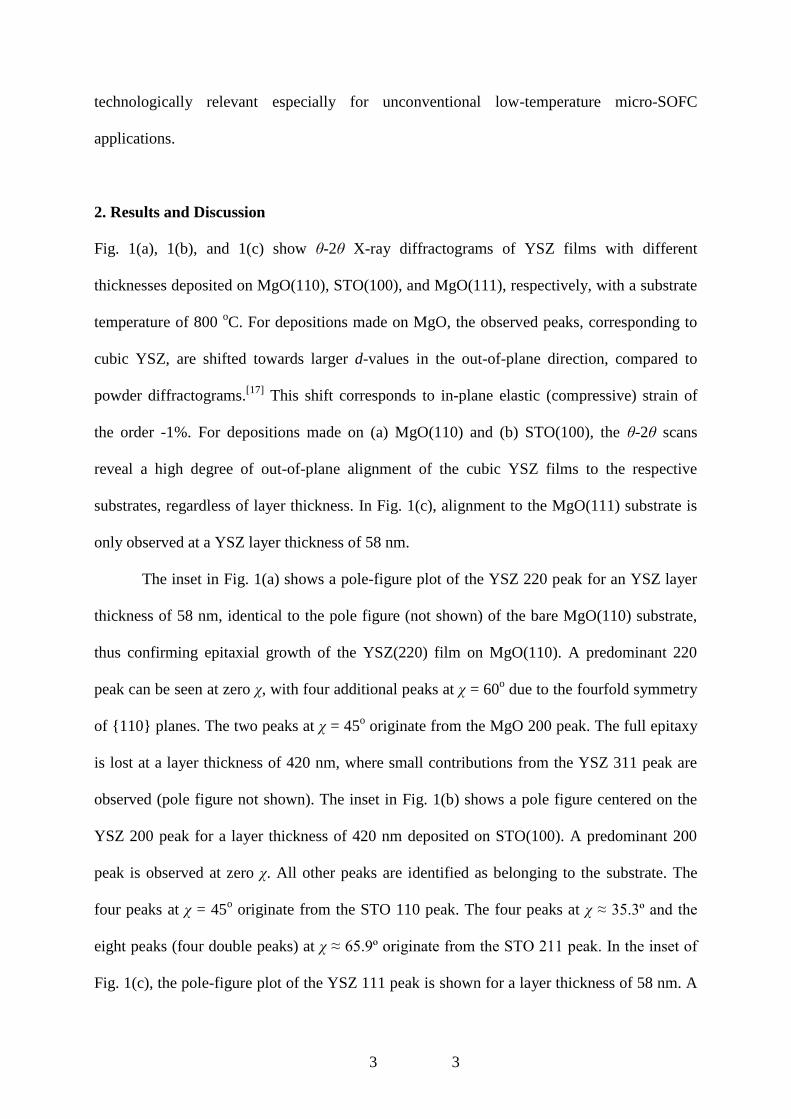
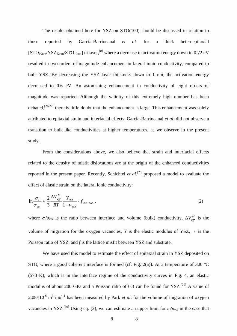
Fig. 2(a) displays a representative high-resolution TEM (HRTEM) image of the
YSZ/STO interface region, showing good crystalline quality of the sample, and (inset) the
selected area electron diffraction (SAED) pattern across the interface along the (110) direction.
The YSZ/STO interface is seen to be continuous and flat but with some slight distortion of the
first atomic layers of the YSZ interface region. Most importantly, the YSZ shows good
structural coherence with the STO crystal, in agreement with the X-ray diffraction (XRD)
results (cf. Fig. 1(b)), meaning that the YSZ layer grows rotated by 45º around the c-axis and
strains to match the STO lattice in the ab-plane. This ensures a large, in-plane expansive
strain in the YSZ interface layer of 7.37% (aYSZ/ 2 = 3.64 Å, aSTO = 3.90 Å), thereby
creating distortion of the first atomic layers of YSZ. The epitaxial strain results in periodic
strain contours, which can be seen from low-magnification images of the YSZ/STO TEM
cross section (not shown). Fig. 2(b) shows a HRTEM image of the interface region of YSZ
deposited onto MgO(110) (the highlighted region marked (c) in Fig. 2(b) is shown magnified
in Fig. 2(c)). The inset in Fig. 2(b) shows an SAED pattern across the YSZ/MgO interface
along the (001) direction, thus confirming the cube-on-cube growth. However, compared to
the relatively flat YSZ/STO interface in Fig. 2(a), a more open and disordered YSZ/MgO
interface region is revealed in the main of Fig. 2(b). The very large lattice misfit (-18.01%)
between YSZ (aYSZ = 5.14 Å) and MgO (aMgO = 4.22 Å) cannot be compensated solely by
elastic strain. Hence, relaxation occurs by the introduction of misfit dislocations at the
YSZ/MgO interface, as shown in Fig. 2(c). An irregular, high density misfit dislocation
network extends along the entire YSZ/MgO interface, which reduces the residual elastic strain
to the order -1% (cf. Fig. 1(a)). Consequently, the growth mode of the YSZ layer is relaxed
heteroepitaxial growth through the formation of a semicoherent YSZ/MgO phase boundary.
5 5
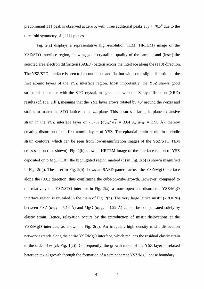
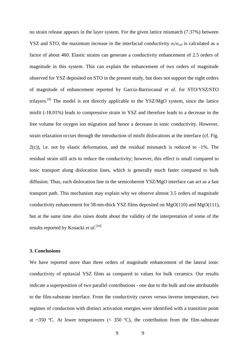
The TEM and X-ray studies confirm the epitaxial growth of the YSZ thin films which
appear to have negligible grain boundaries parallel to the substrate. This ensures that the
lateral current flow is not influenced by grain boundaries. For the usual frequency range f = 1
Hz to 1 MHz, and assuming the absence of inductive effects, many ionic conductors obey the
following relation:[18]
)()0(' fp , (1)
where σ' is the real part of the ac conductivity, σ(0) is the extrapolation of the ac conductivity
to zero frequency, i.e. the dc conductivity σdc, and σp(f) is the polarization conductivity. We
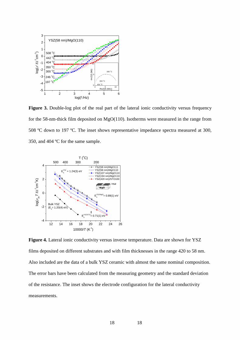
have plotted isotherms of the lateral conductivity (real part σ') of the thinnest YSZ layer on
MgO(110) versus frequency in a double logarithmic plot (Fig. 3). A typical response of ionic
conductors is observed in the figure.[19,20]
The σdc value is found to be thermally activated. At
high temperatures, the dc conductivity dominates almost over the entire frequency range, and
at lower temperatures, the conductivity curves are shifted downwards, and the dc conductivity
is only found at lower frequencies. At a measuring temperature of 197 ºC, the conductivity is
entirely polarized throughout the frequency range. No blocking effects due to grain
boundaries or electrodes are observed in Fig. 3. The inset in Fig. 3 shows representative
impedance spectra at 300, 350, and 404 ºC for the same sample. The spectra consist of only
one semicircle, attributed to the sample response, which is slightly asymmetric in the low
frequency range. An equivalent (RQ)R circuit was used in the fitting procedure to obtain the
resistances, R, with Q representing a constant phase element.
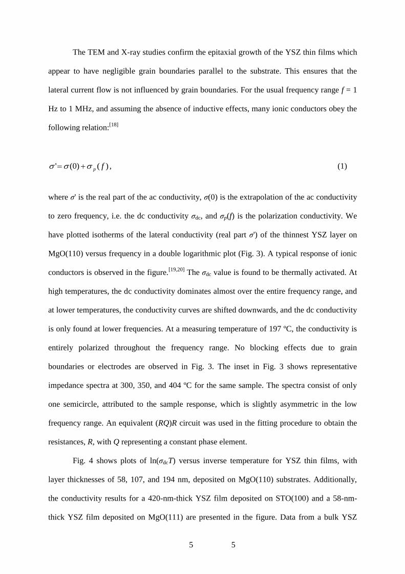
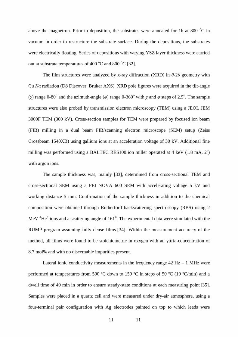
Fig. 4 shows plots of ln(σdcT) versus inverse temperature for YSZ thin films, with
layer thicknesses of 58, 107, and 194 nm, deposited on MgO(110) substrates. Additionally,
the conductivity results for a 420-nm-thick YSZ film deposited on STO(100) and a 58-nm-
thick YSZ film deposited on MgO(111) are presented in the figure. Data from a bulk YSZ
6 6
ceramic (~8.0 mol% Y2O3) have been included as reference. Two regimes of the conductivity
curves are identified with a transition occurring at a temperature of ~350 ºC. These regimes
are characteristic of very distinct activation energies for oxygen ion migration, which have
been found by fitting the linear segments to an Arrhenius expression. At low temperatures (<
350 ºC) an activation energy of 0.89(1) eV is obtained for YSZ films deposited on MgO(110)
and MgO(111) substrates, while an activation energy of 0.71(1) eV is obtained for YSZ
deposited on STO(100). At higher temperatures, an activation energy of 1.24(3) eV is
obtained for all measured samples, which is very close to the value 1.20(4) eV,[21]
obtained
for a bulk YSZ ceramic with the same measurement conditions. Furthermore, the figure
reveals that the conductivity curves shift almost linearly upwards as the YSZ film thickness is
decreased, exhibiting an enhancement in ionic conductivity of roughly 3.5 orders of
magnitude for 58-nm-thick YSZ films deposited on MgO(110) or MgO(111) as compared to
conductivity values for the bulk YSZ. However, no apparent influence of the film orientation
is observed. For these samples in particular, we report a maximum lateral conductivity value
of ~1 Ω-1
cm-1
, obtained at a measuring temperature of 500 ºC, which is comparable to values
reported for the best superionic conductors,[22]
such as RbAg4I5 and α-AgI.[23,24]
The 420-nm-
thick YSZ sample deposited on STO(100) shows an enhancement in conductivity of two
orders of magnitude compared to bulk YSZ at a measuring temperature of 300 ºC. The biggest
relative conductivity enhancement is found in the lower temperature region.
These observations indicate a superposition of two parallel contributions – one due to
the bulk lattice and one attributable to the film-substrate interface. At lower measuring
temperatures (< 350 ºC), the interfacial contribution dominates the ionic conductivity. This
explains why an increase in the lateral ionic conductivity is observed as the YSZ layer
thickness is decreased. It also explains why different activation energies for oxygen ion
migration are obtained for YSZ deposited on MgO (0.89 eV) and STO (0.71 eV) substrates.
Alternatively, free surface effects may also contribute,[25]
however, this is most unlikely since

7 7
different results are obtained on STO and MgO. At higher temperatures, the O2-
-ions gain
enough thermal energy to overcome the energy barrier (1.24 eV) for ionic conduction through
vacancies in the lattice, hence a more “bulk-like” conductivity is obtained. Even though the
conductivity is dominated by bulk lattice diffusion at higher measuring temperatures, still an
interface contribution is present.
The conductivity values found here for 58-nm-thick YSZ films on MgO are
approximately one order of magnitude higher than those obtained by Kosacki et al.[10]
for
ultra-thin (15 nm) YSZ films grown on MgO(100) substrates, when comparing conductivities
obtained in the mutual temperature range between 400 ºC and 500 ºC. Kosacki et al.
discussed a transition from lattice to interface controlled diffusivity for film thicknesses below
60 nm, yielding an enhancement in in-plane conductivity. However, for a film thickness of 29
nm, Kosacki et al. observed a transition from bulk conductivity at lower temperatures to
interface-controlled conductivity at a temperature of 650 ºC or higher, accompanied by a
decrease in activation energy (~0.62 eV). In the present work, we observe interfacial
contributions at low temperatures (< 350 ºC) for all samples in the thickness range 420 to 58
nm. Furthermore, it seems intuitively reasonable that the transition from interface-controlled
conductivity to a “bulk-like” conductivity will occur as the temperature increases, since the
O2-
-ions gain enough thermal energy to overcome the energy barrier (1.24 eV) for migration
via the oxygen vacancies in the lattice. Our view is supported by the results obtained by Sata
et al.[7]
for BaF2/CaF2 superlattices, where an enhancement in ionic conductivity of over three
orders of magnitude related to the number of interfaces was reported. At low temperatures the
interfaces control the conductivity, but as the temperature is increased, the F--ions can
overcome the energy barrier for migration through interstitials in the CaF2 lattice. The
discussed discrepancies may be related to the fact that Kosacki et al. state that no indication
for a dislocation network in the interface was found,[10]
which is most surprising given the
lattice misfit of -18.01%.
8 8
The results obtained here for YSZ on STO(100) should be discussed in relation to
those reported by Garcia-Barriocanal et al. for a thick heteroepitaxial
[STO10nm/YSZ62nm/STO10nm] trilayer,[8]
where a decrease in activation energy down to 0.72 eV
resulted in two orders of magnitude enhancement in lateral ionic conductivity, compared to
bulk YSZ. By decreasing the YSZ layer thickness down to 1 nm, the activation energy
decreased to 0.6 eV. An astonishing enhancement in conductivity of eight orders of
magnitude was reported. Although the validity of this extremely high number has been
debated,[26,27]
there is little doubt that the enhancement is large. This enhancement was solely
attributed to epitaxial strain and interfacial effects. Garcia-Barriocanal et al. did not observe a
transition to bulk-like conductivities at higher temperatures, as we observe in the present
study.
From the considerations above, we also believe that strain and interfacial effects
related to the density of misfit dislocations are at the origin of the enhanced conductivities
reported in the present paper. Recently, Schichtel et al.[28]
proposed a model to evaluate the
effect of elastic strain on the lateral ionic conductivity:
./13
2ln SubYSZ
YSZ
YSZ
M
V
vol
i fY
RT
VO
, (2)
where σi/σvol is the ratio between interface and volume (bulk) conductivity, M
VO
V is the
volume of migration for the oxygen vacancies, Y is the elastic modulus of YSZ, ν is the
Poisson ratio of YSZ, and f is the lattice misfit between YSZ and substrate.
We have used this model to estimate the effect of epitaxial strain in YSZ deposited on
STO, where a good coherent interface is formed (cf. Fig. 2(a)). At a temperature of 300 ºC
(573 K), which is in the interface regime of the conductivity curves in Fig. 4, an elastic
modulus of about 200 GPa and a Poisson ratio of 0.3 can be found for YSZ.[29]
A value of
2.08×10⁻⁶
m3 mol
-1 has been measured by Park et al. for the volume of migration of oxygen
vacancies in YSZ.[30]
Using eq. (2), we can estimate an upper limit for σi/σvol in the case that
9 9
no strain release appears in the layer system. For the given lattice mismatch (7.37%) between
YSZ and STO, the maximum increase in the interfacial conductivity σi/σvol is calculated as a
factor of about 460. Elastic strains can generate a conductivity enhancement of 2.5 orders of
magnitude in this system. This can explain the enhancement of two orders of magnitude
observed for YSZ deposited on STO in the present study, but does not support the eight orders
of magnitude of enhancement reported by Garcia-Barriocanal et al. for STO/YSZ/STO
trilayers.[8]
The model is not directly applicable to the YSZ/MgO system, since the lattice
misfit (-18.01%) leads to compressive strain in YSZ and therefore leads to a decrease in the
free volume for oxygen ion migration and hence a decrease in ionic conductivity. However,
strain relaxation occurs through the introduction of misfit dislocations at the interface (cf. Fig.
2(c)), i.e. not by elastic deformation, and the residual mismatch is reduced to -1%. The
residual strain still acts to reduce the conductivity; however, this effect is small compared to
ionic transport along dislocation lines, which is generally much faster compared to bulk
diffusion. Thus, each dislocation line in the semicoherent YSZ/MgO interface can act as a fast
transport path. This mechanism may explain why we observe almost 3.5 orders of magnitude
conductivity enhancement for 58-nm-thick YSZ films deposited on MgO(110) and MgO(111),
but at the same time also raises doubt about the validity of the interpretation of some of the
results reported by Kosacki et al.[10]
3. Conclusions
We have reported more than three orders of magnitude enhancement of the lateral ionic
conductivity of epitaxial YSZ films as compared to values for bulk ceramics. Our results
indicate a superposition of two parallel contributions - one due to the bulk and one attributable
to the film-substrate interface. From the conductivity curves versus inverse temperature, two
regimes of conduction with distinct activation energies were identified with a transition point
at ~350 ºC. At lower temperatures (< 350 ºC), the contribution from the film-substrate

10 10
interface is dominating, accompanied by a decrease in activation energy, whereas at higher
temperatures a more “bulk-like” conductivity is observed with activation energies comparable
to the activation energy obtained for a bulk YSZ ceramic. The effect of epitaxial strain on the
lateral ionic conductivity was estimated by the strain model proposed by Schichtel et al,[28]
and may fully explain the observed enhancement in conductivity for YSZ deposited on STO.
In the YSZ/MgO system, a high density of misfit dislocations at the semicoherent interface
leads to even larger conductivity enhancements and even superionic conductivities (~1 Ω-1
cm-
1) are achieved.
Our results show that the lateral ionic properties of epitaxial nanoscale YSZ films can
be tailored by controlling the layer thickness and lattice mismatch to the substrate. These very
high ionic conductivities in the temperature range 150 – 500 ºC are of great fundamental
interest and of potential relevance for low-to-medium-temperature applications.
4. Experimental
Depositions were carried out in an ultra high vacuum system with a base pressure < 1×10⁻⁷
Pa,
using reactive direct current (DC) magnetron sputtering of a Zr-Y alloy (84 - 16 at.%) target
with a diameter of 50.8 mm and a thickness of 4 mm mounted facing the target at a constant
power of 75 W. The target-to-substrate distance was 11 cm. A deposition rate of ~9 nm/ min
was obtained at a working pressure of 0.5 Pa with a gas mixture of Ar (99.9997%) and O2
(99.9995%) with an Ar:O2 flow ratio of 68:3.6 sccm. No hysteresis was observed in the
system due to large pumping speeds and relatively small targets. Further details concerning
the growth chamber can be found elsewhere [31].
Cubic perovskite SrTiO3(100) (STO), and face-centered cubic MgO(110), and
MgO(111) single crystals were used as substrates for the YSZ depositions. The substrates
were ultrasonically cleaned in acetone and 2-isopropanol, and dried in pure N2 before they
were inserted into the vacuum chamber. The substrates were mounted on a rotating holder
11 11
above the magnetron. Prior to deposition, the substrates were annealed for 1h at 800 oC in
vacuum in order to restructure the substrate surface. During the depositions, the substrates
were electrically floating. Series of depositions with varying YSZ layer thickness were carried
out at substrate temperatures of 400 oC and 800
oC [32].
The film structures were analyzed by x-ray diffraction (XRD) in θ-2θ geometry with
Cu Kα radiation (D8 Discover, Bruker AXS). XRD pole figures were acquired in the tilt-angle
(χ) range 0-80o and the azimuth-angle (φ) range 0-360
o with χ and φ steps of 2.5
o. The sample
structures were also probed by transmission electron microscopy (TEM) using a JEOL JEM
3000F TEM (300 kV). Cross-section samples for TEM were prepared by focused ion beam
(FIB) milling in a dual beam FIB/scanning electron microscope (SEM) setup (Zeiss
Crossbeam 1540XB) using gallium ions at an acceleration voltage of 30 kV. Additional fine
milling was performed using a BALTEC RES100 ion miller operated at 4 keV (1.8 mA, 2º)
with argon ions.
The sample thickness was, mainly [33], determined from cross-sectional TEM and
cross-sectional SEM using a FEI NOVA 600 SEM with accelerating voltage 5 kV and
working distance 5 mm. Confirmation of the sample thickness in addition to the chemical
composition were obtained through Rutherford backscattering spectroscopy (RBS) using 2
MeV 4He
+ ions and a scattering angle of 161
o. The experimental data were simulated with the
RUMP program assuming fully dense films [34]. Within the measurement accuracy of the
method, all films were found to be stoichiometric in oxygen with an yttria-concentration of
8.7 mol% and with no discernable impurities present.
Lateral ionic conductivity measurements in the frequency range 42 Hz – 1 MHz were
performed at temperatures from 500 ºC down to 150 ºC in steps of 50 ºC (10 ºC/min) and a
dwell time of 40 min in order to ensure steady-state conditions at each measuring point [35].
Samples were placed in a quartz cell and were measured under dry-air atmosphere, using a
four-terminal pair configuration with Ag electrodes painted on top to which leads were
12 12
attached. The separation between the Ag electrodes was 1.5 mm. A Hioki 3250-50 frequency
analyzer was used and the impedance data were analyzed with the software ZSimpWin 3.21
using equivalent circuit fitting [36]. At measurement temperatures of 500 oC and below,
problems related to possible Ag diffusivity could be ruled out.
To evaluate possible substrate contributions, the same setup was used to perform
lateral conductivity measurements on bare MgO(110) and STO(100) substrates. The MgO
substrates yielded resistances beyond the upper range of the frequency analyzer (~1010
Ω).
This shows that the contribution of the MgO substrate on the total resistance was negligible.
The as-prepared STO crystal substrates were stoichiometric and insulating. During vacuum
annealing, prior to YSZ deposition, the STO substrates blackened corresponding to a change
in the material band gap. The modified STO substrates exhibited metallic behavior in terms of
temperature dependence and absolute resistance values. This type of metallic conduction in
STO has been correlated to oxygen deficiencies in the top layer of the STO crystals [37,38].
Allowing a sufficient oxygen flow during pre-deposition annealing of the STO substrates
made it possible to retain the insulating nature of STO to the order ~109 Ω.
Acknowledgements
The authors would like to thank Jacques Chevallier for technical assistance, Karl Thyden of
Risø - DTU for TEM sample preparation, and the Danish Ministry of Science, Technology,
and Development for financial support. P. E. acknowledges funding from the Carlsberg
Foundation, the Swedish Research Council (VR), and the Swedish Foundation for Strategic
Research (SSF).
13 13
References
[1] J. Maier, Solid State Ionics 2000, 131, 13.
[2] M. G. Bellino, D. G. Lamas, and N. E. Walsöe de Reca, Adv. Funct. Mater. 2006, 16,
107.
[3] J. Maier, J. Eur. Ceram. Soc. 2004, 24, 1251.
[4] A. V. Chadwick, Phys. Stat. Sol. A 2007, 204, 631.
[5] G. Knöner, K. Reimann, R. Röwer, U. Södervall, H.-E. Schaefer, Proc. Natl. Acad.
Sci. U.S.A. 2003, 100, 3870.
[6] U. Brossman, G. Knöner, H.-E. Schaefer, R. Würschum, Rev. Adv. Mater. Sci. 2004,
6, 7.
[7] N. Sata, K. Eberman, K. Eberl, and J. Maier, Nature 2000, 408, 946.
[8] J. Garcia-Barriocanal, A. Rivera-Calzada, M. Varela, Z. Sefrioui, E. Iborra, C. Leon,
S. J. Pennycook, J. Santamaria, Science 2008, 321, 676.
[9] S. Ramanathan, J. Vac. Sci. Technol. A 2009, 27, 1126.
[10] I. Kosacki, C. M. Rouleau, P. F. Becher, J. Bentley, D. H. Lowndes, Solid State Ionics
2005, 176, 1319.
[11] L. Chen, C. L. Chen, X. Chen, W. Donner, S. W. Liu, Y. Lin, D. X. Huang, A. J.
Jacobson, Appl. Phys. Lett. 2003, 83, 4737.
[12] B. C. H. Steele, J. Power Sources 1994, 49, 1.
[13] S. P. S. Badwal, K. Foger, Ceram. Int. 1996, 22, 257.
[14] J. B. Goodenough, Annu. Rev. Mater. Res. 2003, 33, 91.
[15] M. Sillassen, P. Eklund, M. Sridharan, N. Pryds, N. Bonanos, J. Bøttiger, J. Appl.
Phys. 2009, 105, 10.
[16] H. L. Tuller, Solid State Ionics 2000, 131, 143.
[17] JCPDS Card No. 82-1246.

14 14
[18] F. E. G. Henn, R. M. Buchanan, N. Jiang, D. A. Stevenson, Appl. Phys. A 1995, 60,
515.
[19] A. K. Jonscher, Nature 1977, 267, 673.
[20] C. A. Angell, Chem Rev. 1990, 90, 523.
[21] This value is slightly higher than those reported in literature for bulk YSZ (~1.1 eV).
This is likely due to the choice of atmosphere during measurements. Generally, the
lowest activation energies are obtained in pure oxygen atmospheres.
[22] Although regarded a misnomer by some, “superionic” conductors are usually defined
as solid state systems that display ionic conductivities that are typical of those found in
molten salts, i.e., σ ~1 Ω-1
cm-1
.[23]
[23] J. B. Boyce, B. A. Huberman, Phys. Rep. 1979, 51, 189.
[24] A. R. West, in Basic Solid State Chemistry, 2nd Ed., John Wiley & Sons, Chichester,
England 1999, Ch. 7.
[25] A. Karthikeyan, C.-L. Chang, S. Ramanathan, Appl. Phys. Lett. 2006, 89, 183116.
[26] X. Guo, Science 2009, 324, 465-a.
[27] J. Garcia-Barriocanal, A. Rivera-Calzada, M. Varela, Z. Sefrioui, E. Iborra, C. Leon,
S. J. Pennycook, J. Santamaria, Science 2009, 324, 465-b.
[28] N. Schichtel, C. Korte, D. Hesse, J. Janek, Phys. Chem. Chem. Phys. 2009, 11, 3043.
[29] H. M. Kandil, J. D. Greiner, J. F. Smith, J. Am. Ceram. Soc. 1984, 67, 341.
[30] E. T. Park, J.-H. Park, in Proceedings of the 3rd
International Meeting of Pacific Rim
Ceramic Societies, Kyungju, Korea 1998.
[31] E. Wallin, J. M. Andersson, M. Latteman, U. Helmersson, Thin Solid Films 2008, 516,
3877.

15 15
[32] At a substrate temperature of 400 oC, epitaxial YSZ films could only be grown on
MgO(110) substrates, but with much less X-ray intensity of the observed YSZ 220
peaks (not shown). Depositions made on STO(100) and MgO(111) at a substrate
temperature of 400 oC yielded polycrystalline YSZ films with a preferred <111>
texture for all layer thicknesses.
[33] Film thicknesses less than 100 nm were determined by X-ray reflectivity (XRR)
measurements.
[34] L. R. Doolittle, Nucl. Instrum. Methods Phys. Res., B Beam Interact. Mater. Atoms
1985, 9, 344.
[35] Measurements on the sample deposited on MgO(111) were performed from 450 ºC
down to 200 ºC in steps of 25 ºC.
[36] ZSimpWin 3.21, EChem Software, Bruno Deum, Ann Arbor, Michigan, USA, 1999-
2005.
[37] D. Kan, T. Terashima, R. Kanda, A. Masuno, K. Tanaka, S. Chu, H. Kan, A. Ishizumi,
Y. Kanemitsu, Y. Shimakawa, M. Takano, Nature Mater. 2005, 4, 816.
[38] J. C. C. Abrantes, J. A. Labrincha, J. R. Frade, J. Eur. Ceram. Soc. 2002, 22, 1683.
16 16
20 30 40 50 60 7010
0
101
102
103
104
105
106
107
Measured PF 220
Inte
nsity (
Cps)
2 (degrees)
420 nm
194 nm
107 nm
58 nm
YS
Z220
MgO
110
(a)
20 30 40 50 60 7010
0
101
102
103
104
105
106
107
Measured PF 200
CuK
YS
Z200
ST
O200
ST
O100
Inte
nsity (
Cp
s)
2 (degrees)
420 nm
285 nm
194 nm
107 nm
58 nm
(b)
20 30 40 50 60 7010
0
101
102
103
104
105
106
107
Measured PF 111
YS
Z222
YS
Z200
MgO
111
Inte
nsity (
Cp
s)
2 (degrees)
107 nm
58 nm
YS
Z111
(c)
Figure 1. θ-2θ X-ray diffractograms of YSZ films with different layer thicknesses, deposited
at 800 oC on (a) MgO(110), (b) STO(100), and (c) MgO(111) single crystals. Insets show pole
figures centered on the respective YSZ peaks for YSZ layer thicknesses of (a) 58 nm, (b) 420
nm, and (c) 58 nm.

17 17
Figure 2. (a) HRTEM image of the YSZ/STO interface region. The inset in (a) shows the
SAED pattern across the YSZ/STO interface along the YSZ(110) direction. (b) HRTEM
image of the YSZ/MgO interface region. The inset in (b) shows the SAED pattern across the
YSZ/MgO interface along the YSZ(100) direction. (c) Magnification of the area marked in (b).
Misfit dislocations are indicated by T symbols in (c).
18 18
1 2 3 4 5 6-5
-4
-3
-2
-1
0
1
2
3
0 5 100
5
10
-Im
Z(f
) (M
)ReZ(f) (M)
404 oC
350 oC
300 oC
197 oC
246 oC
300 oC
350 oC
404 oC
442 oC
log(
' /
-1cm
-1)
log(f /Hz)
508 oC
YSZ(58 nm)/MgO(110)
Figure 3. Double-log plot of the real part of the lateral ionic conductivity versus frequency
for the 58-nm-thick film deposited on MgO(110). Isotherms were measured in the range from
508 ºC down to 197 ºC. The inset shows representative impedance spectra measured at 300,
350, and 404 ºC for the same sample.
12 14 16 18 20 22 24 26-4
-2
0
2
4200300400
M gO
YSZ
M gOM gO
YSZ
EYSZ/STO
a= 0.71(1) eV
EYSZ/MgO
a= 0.89(1) eV
EYSZ
a = 1.24(3) eV
log
(d
cT
/
-1cm
-1K
)
10000/T (K-1)
YSZ(58 nm)/MgO111
YSZ(58 nm)/MgO110
YSZ(107 nm)/MgO110
YSZ(194 nm)/MgO110
YSZ(420 nm)/STO100
500
T (oC)
Bulk YSZ
(Ea= 1.20(4) eV)
Figure 4. Lateral ionic conductivity versus inverse temperature. Data are shown for YSZ
films deposited on different substrates and with film thicknesses in the range 420 to 58 nm.
Also included are the data of a bulk YSZ ceramic with almost the same nominal composition.
The error bars have been calculated from the measuring geometry and the standard deviation
of the resistance. The inset shows the electrode configuration for the lateral conductivity
measurements.

19 19


