LM6181100 mA, 100 MHz Current Feedback AmplifierGeneral DescriptionThe LM6181 current-feedback amplifier offers an unparal-leled combination of bandwidth, slew-rate, and output cur-rent. The amplifier can directly drive up to 100 pF capacitiveloads without oscillating and a 10V signal into a 50Ω or 75Ωback-terminated coax cable system over the full industrialtemperature range. This represents a radical enhancementin output drive capability for an 8-pin DIP high-speed ampli-fier making it ideal for video applications.
Built on National’s advanced high-speed VIP™ II (VerticallyIntegrated PNP) process, the LM6181 employs current-feedback providing bandwidth that does not vary dramati-cally with gain; 100 MHz at AV = −1, 60 MHz at AV = −10.With a slew rate of 2000V/µs, 2nd harmonic distortion of −50dBc at 10 MHz and settling time of 50 ns (0.1%) the LM6181dynamic performance makes it ideal for data acquisition,high speed ATE, and precision pulse amplifier applications.
Features(Typical unless otherwise noted)n Slew rate: 2000 V/µsn Settling time (0.1%): 50 nsn Characterized for supply ranges: ±5V and ±15Vn Low differential gain and phase error: 0.05%, 0.04˚n High output drive: ±10V into 100Ωn Guaranteed bandwidth and slew raten Improved performance over EL2020, OP160, AD844,
LT1223 and HA5004
Applicationsn Coax cable drivern Video amplifiern Flash ADC buffern High frequency filtern Scanner and Imaging systems
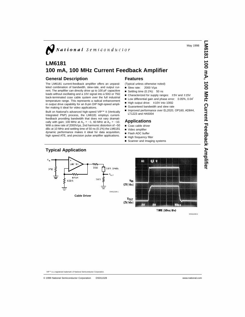
Typical Application
VIP™ is a registered trademark of National Semiconductor Corporation.
DS011328-1
Cable Driver
DS011328-2
May 1998
LM6181
100m
A,100
MH
zC
urrentFeedbackA
mplifier
© 1999 National Semiconductor Corporation DS011328 www.national.com
Absolute Maximum Ratings (Note 1)
If Military/Aerospace specified devices are required,please contact the National Semiconductor Sales Office/Distributors for availability and specifications.
Supply Voltage ±18VDifferential Input Voltage ±6VInput Voltage ±Supply VoltageInverting Input Current 15 mASoldering Information
Dual-In-Line Package (N)Soldering (10 sec) 260˚C
Small Outline Package (M)Vapor Phase (60 seconds) 215˚CInfrared (15 seconds) 220˚C
Output Short Circuit (Note 7)
Storage Temperature Range −65˚C ≤ TJ ≤ +150˚CMaximum Junction Temperature 150˚CESD Rating (Note 2) ±3000V
Operating RatingsSupply Voltage Range 7V to 32VJunction Temperature Range (Note 3)
LM6181AM −55˚C ≤ TJ ≤ +125˚CLM6181AI, LM6181I −40˚C ≤ TJ ≤ +85˚C
Thermal Resistance (θJA, θJC)8-pin DIP (N) 102˚C/W, 42˚C/W8-pin SO (M-8) 153˚C/W, 42˚C/W
16-pin SO (M) 70˚C/W, 38˚C/W
±15V DC Electrical CharacteristicsThe following specifications apply for Supply Voltage = ±15V, RF = 820Ω, and RL = 1 kΩ unless otherwise noted. Boldfacelimits apply at the temperature extremes; all other limits TJ = 25˚C.
Symbol Parameter Conditions LM6181AM LM6181AI LM6181I Units
Typical Limit Typical Limit Typical Limit
(Note 4) (Note 5) (Note 4) (Note 5) (Note 4) (Note 5)
VOS Input Offset Voltage 2.0 3.0 2.0 3.0 3.5 5.0 mV
4.0 3.5 5.5 max
TCVOS
Input Offset Voltage Drift 5.0 5.0 5.0 µV/˚C
IB Inverting Input Bias Current 2.0 5.0 2.0 5.0 5.0 10 µAmax
12.0 12.0 17.0
Non-Inverting Input Bias Current 0.5 1.5 0.5 1.5 2.0 3.0
3.0 3.0 5.0
TC IB Inverting Input Bias Current Drift 30 30 30 nA/˚C
Non-Inverting Input Bias 10 10 10
Current Drift
IB Inverting Input Bias Current VS = ±4.5V, ±16V 0.3 0.5 0.3 0.5 0.3 0.75 µA/Vmax
PSR Power Supply Rejection 3.0 3.0 4.5
Non-Inverting Input Bias Current VS = ±4.5V, ±16V 0.05 0.5 0.05 0.5 0.05 0.5
Power Supply Rejection 1.5 1.5 3.0
IB Inverting Input Bias Current −10V ≤ VCM ≤ +10V 0.3 0.5 0.3 0.5 0.3 0.75
CMR Common Mode Rejection 0.75 0.75 1.0
Non-Inverting Input Bias Current −10V ≤ VCM ≤ +10V 0.1 0.5 0.1 0.5 0.1 0.5
Common Mode Rejection 0.5 0.5 0.5
CMRR Common Mode Rejection Ratio −10V ≤ VCM ≤ +10V 60 50 60 50 60 50 dB
50 50 50 min
PSRR Power Supply Rejection Ratio VS = ±4.5V, ±16V 80 70 80 70 80 70 dB
70 70 65 min
RO Output Resistance AV = −1, f = 300 kHz 0.2 0.2 0.2 Ω
RIN Non-Inverting Input Resistance 10 10 10 MΩ
min
VO Output Voltage Swing RL = 1 kΩ 12 11 12 11 12 11 Vmin
11 11 11
RL = 100Ω 11 10 11 10 11 10
7.5 8.0 8.0
ISC Output Short Circuit Current 130 100 130 100 130 100 mA
75 85 85 min
www.national.com 2
±15V DC Electrical Characteristics (Continued)
The following specifications apply for Supply Voltage = ±15V, RF = 820Ω, and RL = 1 kΩ unless otherwise noted. Boldfacelimits apply at the temperature extremes; all other limits TJ = 25˚C.
Symbol Parameter Conditions LM6181AM LM6181AI LM6181I Units
Typical Limit Typical Limit Typical Limit
(Note 4) (Note 5) (Note 4) (Note 5) (Note 4) (Note 5)
ZT Transimpedance RL = 1 kΩ 1.8 1.0 1.8 1.0 1.8 0.8
0.5 0.5 0.4 MΩ
RL = 100Ω 1.4 0.8 1.4 0.8 1.4 0.7 min
0.4 0.4 0.35
IS Supply Current No Load, VO = 0V 7.5 10 7.5 10 7.5 10 mA
10 10 10 max
VCM Input Common Mode V+ − 1.7V V+ − 1.7V V+ − 1.7V V
Voltage Range V− + 1.7V V− + 1.7V V− + 1.7V
±15V AC Electrical CharacteristicsThe following specifications apply for Supply Voltage = ±15V, RF = 820Ω, RL = 1 kΩ unless otherwise noted. Boldface limitsapply at the temperature extremes; all other limits TJ = 25˚C.
Symbol Parameter Conditions LM6181AM LM6181AI LM6181I Units
Typical Limit Typical Limit Typical Limit
(Note 4) (Note 5) (Note 4) (Note 5) (Note 4) (Note 5)
BW Closed Loop Bandwidth AV = +2 100 100 100 MHzmin
−3 dB AV = +10 80 80 80
AV = −1 100 80 100 80 100 80
AV = −10 60 60 60
PBW Power Bandwidth AV = −1, VO = 5 VPP 60 60 60
SR Slew Rate Overdriven 2000 2000 2000 V/µsmin
AV = −1, VO = ±10V, 1400 1000 1400 1000 1400 1000
RL = 150Ω (Note 6)
ts Settling Time (0.1%) AV = −1, VO = ±5V 50 50 50 ns
RL = 150Ω
tr, tf Rise and Fall Time VO = 1 VPP 5 5 5
tp Propagation Delay Time VO = 1 VPP 6 6 6
in(+) Non-Inverting Input Noise f = 1 kHz 3 3 3
Current Density
in(−) Inverting Input Noise f = 1 kHz 16 16 16
Current Density
en Input Noise VoltageDensity
f = 1 kHz 4 4 4
Second Harmonic Distortion 2 VPP, 10 MHz −50 −50 −50 dBc
Third Harmonic Distortion 2 VPP, 10 MHz −55 −55 −50
Differential Gain RL = 150Ω
AV = +2 0.05 0.05 0.05 %
NTSC
Differential Phase RL = 150Ω
AV = +2 0.04 0.04 0.04 Deg
NTSC
www.national.com3
±5V DC Electrical CharacteristicsThe following specifications apply for Supply Voltage = ±5V, RF = 820Ω, and RL = 1 kΩ unless otherwise noted. Boldfacelimits apply at the temperature extremes; all other limits TJ = 25˚C.
Symbol Parameter Conditions LM6181AM LM6181AI LM6181I Units
Typical Limit Typical Limit Typical Limit
(Note 4) (Note 5) (Note 4) (Note 5) (Note 4) (Note 5)
VOS Input Offset Voltage 1.0 2.0 1.0 2.0 1.0 3.0 mV
3.0 2.5 3.5 max
TCVOS
Input Offset Voltage Drift 2.5 2.5 2.5 µV/˚C
IB Inverting Input 5.0 10 5.0 10 5.0 17.5 µAmax
Bias Current 22 22 27.0
Non-Inverting Input 0.25 1.5 0.25 1.5 0.25 3.0
Bias Current 1.5 1.5 5.0
TC IB Inverting Input Bias 50 50 50 nA/˚C
Current Drift
Non-Inverting Input 3.0 3.0 3.0
Bias Current Drift
IB Inverting Input Bias Current VS = ±4.0V, ±6.0V 0.3 0.5 0.3 0.5 0.3 1.0 µA/Vmax
PSR Power Supply Rejection 0.5 0.5 1.0
Non-Inverting Input VS = ±4.0V, ±6.0V 0.05 0.5 0.05 0.5 0.05 0.5
Bias Current
Power Supply Rejection 0.5 0.5 0.5
IB Inverting Input Bias Current −2.5V ≤ VCM ≤ +2.5V 0.3 0.5 0.3 0.5 0.3 1.0
CMR Common Mode Rejection 1.0 1.0 1.5
Non-Inverting Input −2.5V ≤ VCM ≤ +2.5V 0.12 0.5 0.12 0.5 0.12 0.5
Bias Current
Common Mode Rejection 1.0 0.5 0.5
CMRR Common Mode −2.5V ≤ VCM ≤ +2.5V 57 50 57 50 57 50 dBmin
Rejection Ratio 47 47 47
PSRR Power Supply VS = ±4.0V, ±6.0V 80 70 80 70 80 64
Rejection Ratio 70 70 64
RO Output Resistance AV = −1, f = 300 kHz 0.25 0.25 0.25 Ω
RIN Non-Inverting 8 8 8 MΩ
Input Resistance min
VO Output Voltage Swing RL = 1 kΩ 2.6 2.25 2.6 2.25 2.6 2.25 Vmin
2.2 2.25 2.25
RL = 100Ω 2.2 2.0 2.2 2.0 2.2 2.0
2.0 2.0 2.0
ISC Output Short 100 75 100 75 100 75 mA
Circuit Current 70 70 70 min
ZT Transimpedance RL = 1 kΩ 1.4 0.75 1.4 0.75 1.0 0.6
0.35 0.4 0.3 MΩ
RL = 100Ω 1.0 0.5 1.0 0.5 1.0 0.4 min
0.25 0.25 0.2
IS Supply Current No Load, VO = 0V 6.5 8.5 6.5 8.5 6.5 8.5 mA
8.5 8.5 8.5 max
VCM Input Common Mode V+ − 1.7V V+ − 1.7V V+ − 1.7V V
Voltage Range V− + 1.7V V− + 1.7V V− + 1.7V
www.national.com 4

±5V AC Electrical CharacteristicsThe following specifications apply for Supply Voltage = ±5V, RF = 820Ω, and RL = 1 kΩ unless otherwise noted. Boldfacelimits apply at the temperature extremes; all other limits TJ = 25˚C.
Symbol Parameter Conditions LM6181AM LM6181AI LM6181I Units
Typical Limit Typical Limit Typical Limit
(Note 4) (Note 5) (Note 4) (Note 5) (Note 4) (Note 5)
BW Closed Loop Bandwidth −3 dB AV = +2 50 50 50 MHzmin
AV = +10 40 40 40
AV = −1 55 35 55 35 55 35
AV = −10 35 35 35
PBW Power Bandwidth AV = −1, VO = 4 VPP 40 40 40
SR Slew Rate AV = −1, VO = ±2V, 500 375 500 375 500 375 V/µs
RL = 150Ω (Note 6) min
ts Settling Time (0.1%) AV = −1, VO = ±2V 50 50 50 ns
RL = 150Ω
tr, tf Rise and Fall Time VO = 1 VPP 8.5 8.5 8.5
tp Propagation Delay Time VO = 1 VPP 8 8 8
in(+) Non-Inverting Input Noise f = 1 kHz 3 3 3
Current Density
in(−) Inverting Input Noise f = 1 kHz 16 16 16
Current Density
en Input Noise VoltageDensity
f = 1 kHz 4 4 4
Second Harmonic Distortion 2 VPP, 10 MHz −45 −45 −45 dBc
Third Harmonic Distortion 2 VPP, 10 MHz −55 −55 −55
Differential Gain RL = 150Ω
AV = +2 0.063 0.063 0.063 %
NTSC
Differential Phase RL = 150Ω
AV = +2 0.16 0.16 0.16 Deg
NTSC
Note 1: Absolute Maximum Ratings indicate limits beyond which damage to the device may occur. Operating ratings indicate conditions the device is intended tobe functional, but device parameter specifications may not be guaranteed under these conditions. For guaranteed specifications and test conditions, see the ElectricalCharacteristics.
Note 2: Human body model 100 pF and 1.5 kΩ.
Note 3: The typical junction-to-ambient thermal resistance of the molded plastic DIP(N) package soldered directly into a PC board is 102˚C/W. Thejunction-to-ambient thermal resistance of the S.O. surface mount (M) package mounted flush to the PC board is 70˚C/W when pins 1, 4, 8, 9 and 16 are solderedto a total 2 in2 1 oz. copper trace. The 16-pin S.O. (M) package must have pin 4 and at least one of pins 1, 8, 9, or 16 connected to V− for proper operation. The typicaljunction-to-ambient thermal resistance of the S.O. (M-8) package soldered directly into a PC board is 153˚C/W.
Note 4: Typical values represent the most likely parametric norm.
Note 5: All limits guaranteed at room temperature (standard type face) or at operating temperature extremes (bold face type) .
Note 6: Measured from +25% to +75% of output waveform.
Note 7: Continuous short circuit operation at elevated ambient temperature can result in exceeding the maximum allowed junction temperature of 150˚C. Output cur-rents in excess of ±130 mA over a long term basis may adversely affect reliability.
Note 8: For guaranteed Military Temperature Range parameters see RETS6181X.
www.national.com5
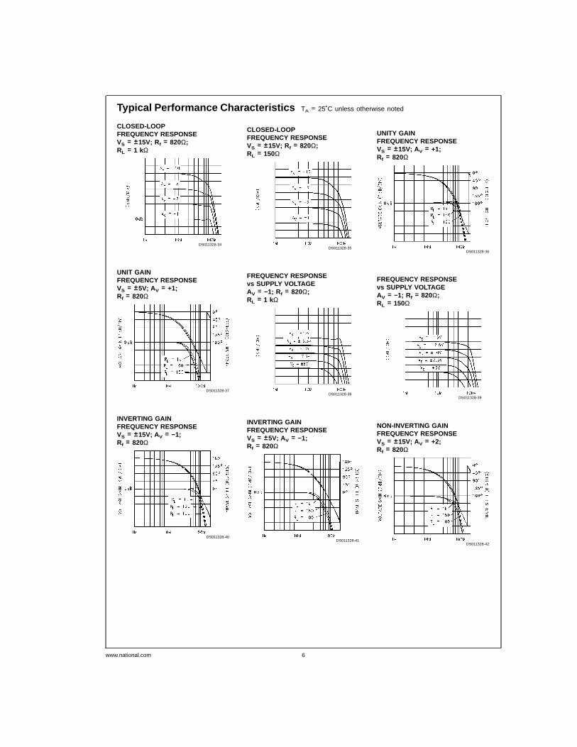
Typical Performance Characteristics TA = 25˚C unless otherwise noted
CLOSED-LOOPFREQUENCY RESPONSEVS = ±15V; Rf = 820Ω;RL = 1 kΩ
DS011328-34
CLOSED-LOOPFREQUENCY RESPONSEVS = ±15V; Rf = 820Ω;RL = 150Ω
DS011328-35
UNITY GAINFREQUENCY RESPONSEVS = ±15V; AV = +1;Rf = 820Ω
DS011328-36
UNIT GAINFREQUENCY RESPONSEVS = ±5V; AV = +1;Rf = 820Ω
DS011328-37
FREQUENCY RESPONSEvs SUPPLY VOLTAGEAV = −1; Rf = 820Ω;RL = 1 kΩ
DS011328-38
FREQUENCY RESPONSEvs SUPPLY VOLTAGEAV = −1; Rf = 820Ω;RL = 150Ω
DS011328-39
INVERTING GAINFREQUENCY RESPONSEVS = ±15V; AV = −1;Rf = 820Ω
DS011328-40
INVERTING GAINFREQUENCY RESPONSEVS = ±5V; AV = −1;Rf = 820Ω
DS011328-41
NON-INVERTING GAINFREQUENCY RESPONSEVS = ±15V; AV = +2;Rf = 820Ω
DS011328-42
www.national.com 6
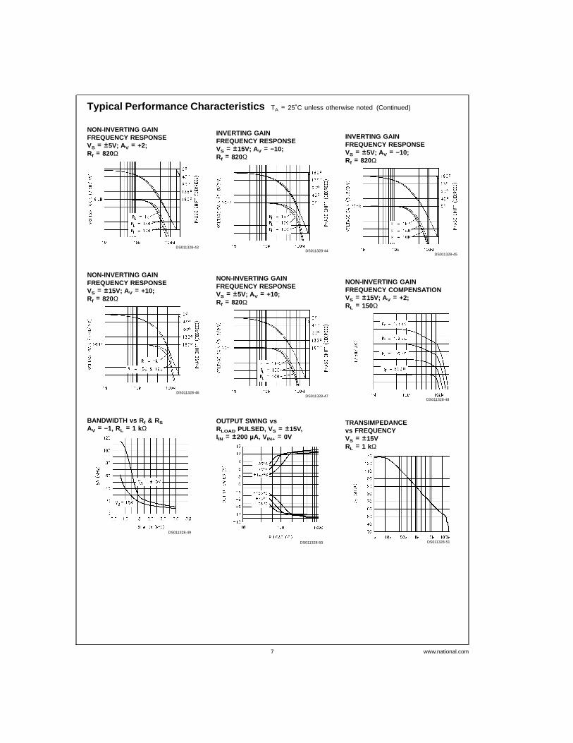
Typical Performance Characteristics TA = 25˚C unless otherwise noted (Continued)
NON-INVERTING GAINFREQUENCY RESPONSEVS = ±5V; AV = +2;Rf = 820Ω
DS011328-43
INVERTING GAINFREQUENCY RESPONSEVS = ±15V; AV = −10;Rf = 820Ω
DS011328-44
INVERTING GAINFREQUENCY RESPONSEVS = ±5V; AV = −10;Rf = 820Ω
DS011328-45
NON-INVERTING GAINFREQUENCY RESPONSEVS = ±15V; AV = +10;Rf = 820Ω
DS011328-46
NON-INVERTING GAINFREQUENCY RESPONSEVS = ±5V; AV = +10;Rf = 820Ω
DS011328-47
NON-INVERTING GAINFREQUENCY COMPENSATIONVS = ±15V; AV = +2;RL = 150Ω
DS011328-48
BANDWIDTH vs R f & RS
AV = −1, RL = 1 kΩ
DS011328-49
OUTPUT SWING vsRLOAD PULSED, VS = ±15V,IIN = ±200 µA, VIN+ = 0V
DS011328-50
TRANSIMPEDANCEvs FREQUENCYVS = ±15VRL = 1 kΩ
DS011328-51
www.national.com7
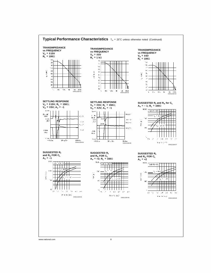
Typical Performance Characteristics TA = 25˚C unless otherwise noted (Continued)
TRANSIMPEDANCEvs FREQUENCYVS = ±15VRL = 100Ω
DS011328-52
TRANSIMPEDANCEvs FREQUENCYVS = ±5VRL = 1 kΩ
DS011328-53
TRANSIMPEDANCEvs FREQUENCYVS = ±5VRL = 100Ω
DS011328-54
SETTLING RESPONSEVS = ±15V; RL = 150Ω;VO = ±5V; AV = −1
DS011328-55
SETTLING RESPONSEVS = ±5V; RL = 150Ω;VO = ±2V; AV = −1
DS011328-56
SUGGESTED Rf and RS for C L
AV = − 1; RL = 150Ω
DS011328-57
SUGGESTED Rf
and RS FOR CL
AV = −1
DS011328-58
SUGGESTED Rf
and RS FOR CL
AV = +2; RL = 150Ω
DS011328-59
SUGGESTED Rf
and RS FOR CL
AV = +2
DS011328-60
www.national.com 8

Typical Performance Characteristics TA = 25˚C unless otherwise noted (Continued)
OUTPUT IMPEDANCEvs FREQVS = ±15V; AV = −1Rf = 820Ω
DS011328-61
OUTPUT IMPEDANCEvs FREQVS = ±5V; AV = −1Rf = 820Ω
DS011328-62
PSRR (VS+) vs FREQUENCY
DS011328-63
PSRR (VS−) vs FREQUENCY
DS011328-64
CMRR vs FREQUENCY
DS011328-65
INPUT VOLTAGE NOISEvs FREQUENCY
DS011328-66
INPUT CURRENTNOISE vs FREQUENCY
DS011328-67
SLEW RATE vsTEMPERATURE AV = −1;RL = 150Ω, VS = ±15V
DS011328-68
SLEW RATE vsTEMPERATURE AV = −1;RL = 150Ω, VS = ±5V
DS011328-69
www.national.com9
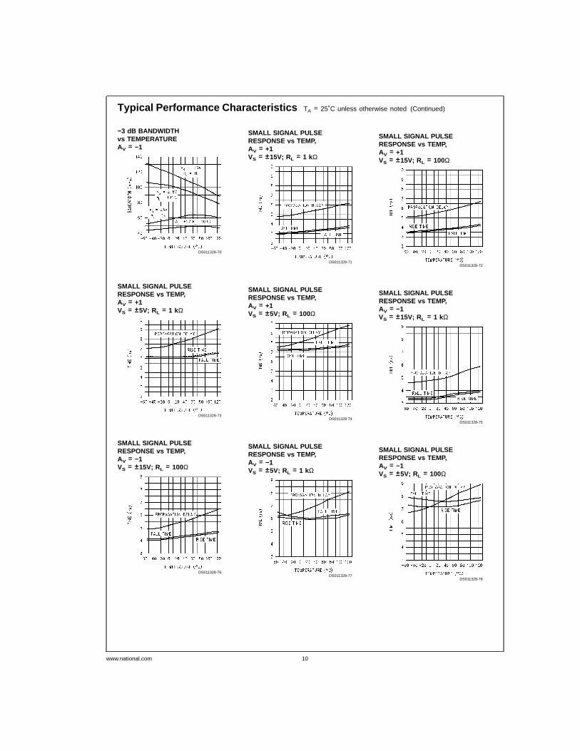
Typical Performance Characteristics TA = 25˚C unless otherwise noted (Continued)
−3 dB BANDWIDTHvs TEMPERATUREAV = −1
DS011328-70
SMALL SIGNAL PULSERESPONSE vs TEMP,AV = +1VS = ±15V; RL = 1 kΩ
DS011328-71
SMALL SIGNAL PULSERESPONSE vs TEMP,AV = +1VS = ±15V; RL = 100Ω
DS011328-72
SMALL SIGNAL PULSERESPONSE vs TEMP,AV = +1VS = ±5V; RL = 1 kΩ
DS011328-73
SMALL SIGNAL PULSERESPONSE vs TEMP,AV = +1VS = ±5V; RL = 100Ω
DS011328-74
SMALL SIGNAL PULSERESPONSE vs TEMP,AV = −1VS = ±15V; RL = 1 kΩ
DS011328-75
SMALL SIGNAL PULSERESPONSE vs TEMP,AV = −1VS = ±15V; RL = 100Ω
DS011328-76
SMALL SIGNAL PULSERESPONSE vs TEMP,AV = −1VS = ±5V; RL = 1 kΩ
DS011328-77
SMALL SIGNAL PULSERESPONSE vs TEMP,AV = −1VS = ±5V; RL = 100Ω
DS011328-78
www.national.com 10
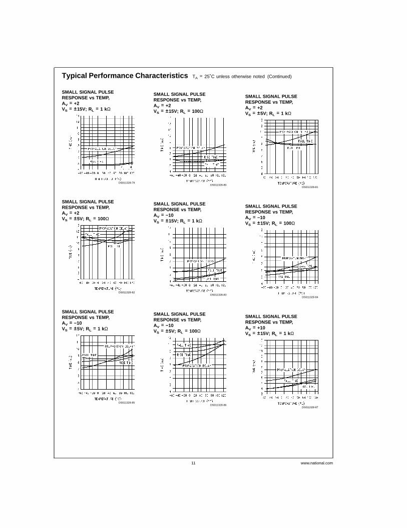
Typical Performance Characteristics TA = 25˚C unless otherwise noted (Continued)
SMALL SIGNAL PULSERESPONSE vs TEMP,AV = +2VS = ±15V; RL = 1 kΩ
DS011328-79
SMALL SIGNAL PULSERESPONSE vs TEMP,AV = +2VS = ±15V; RL = 100Ω
DS011328-80
SMALL SIGNAL PULSERESPONSE vs TEMP,AV = +2VS = ±5V; RL = 1 kΩ
DS011328-81
SMALL SIGNAL PULSERESPONSE vs TEMP,AV = +2VS = ±5V; RL = 100Ω
DS011328-82
SMALL SIGNAL PULSERESPONSE vs TEMP,AV = −10VS = ±15V; RL = 1 kΩ
DS011328-83
SMALL SIGNAL PULSERESPONSE vs TEMP,AV = −10VS = ±15V; RL = 100Ω
DS011328-84
SMALL SIGNAL PULSERESPONSE vs TEMP,AV = −10VS = ±5V; RL = 1 kΩ
DS011328-85
SMALL SIGNAL PULSERESPONSE vs TEMP,AV = −10VS = ±5V; RL = 100Ω
DS011328-86
SMALL SIGNAL PULSERESPONSE vs TEMP,AV = +10VS = ±15V; RL = 1 kΩ
DS011328-87
www.national.com11
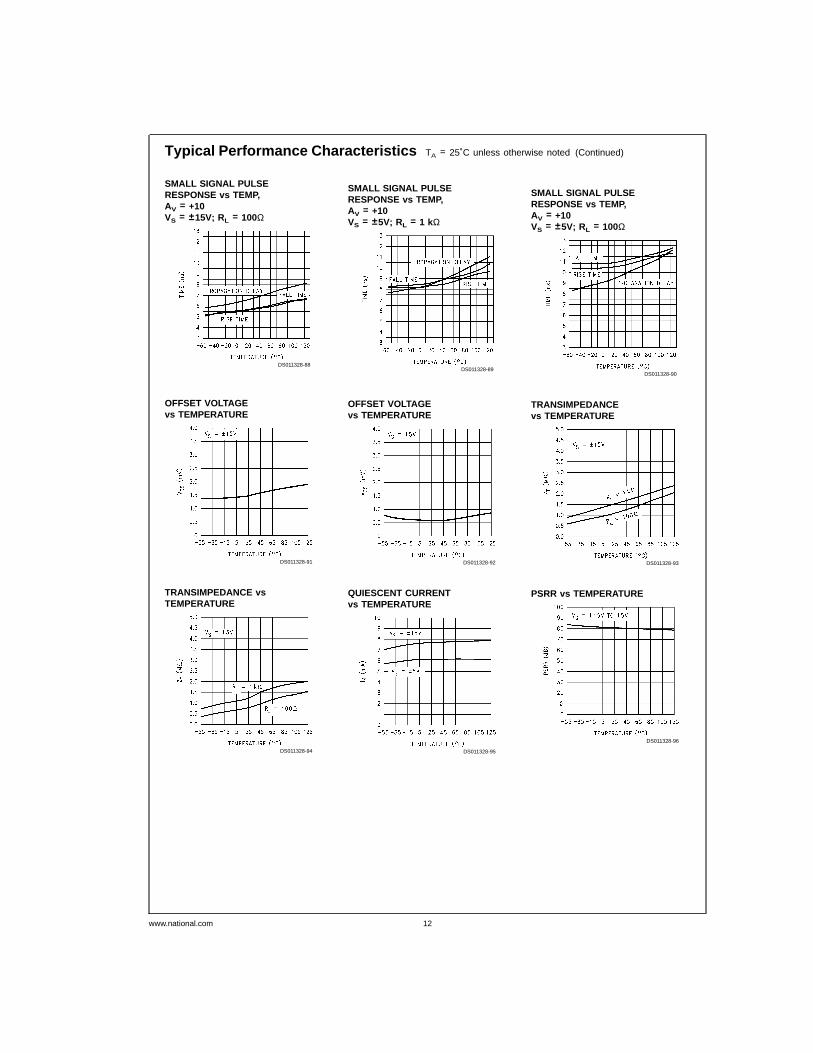
Typical Performance Characteristics TA = 25˚C unless otherwise noted (Continued)
SMALL SIGNAL PULSERESPONSE vs TEMP,AV = +10VS = ±15V; RL = 100Ω
DS011328-88
SMALL SIGNAL PULSERESPONSE vs TEMP,AV = +10VS = ±5V; RL = 1 kΩ
DS011328-89
SMALL SIGNAL PULSERESPONSE vs TEMP,AV = +10VS = ±5V; RL = 100Ω
DS011328-90
OFFSET VOLTAGEvs TEMPERATURE
DS011328-91
OFFSET VOLTAGEvs TEMPERATURE
DS011328-92
TRANSIMPEDANCEvs TEMPERATURE
DS011328-93
TRANSIMPEDANCE vsTEMPERATURE
DS011328-94
QUIESCENT CURRENTvs TEMPERATURE
DS011328-95
PSRR vs TEMPERATURE
DS011328-96
www.national.com 12
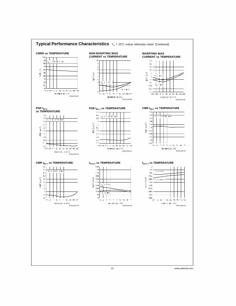
Typical Performance Characteristics TA = 25˚C unless otherwise noted (Continued)
CMRR vs TEMPERATURE
DS011328-97
NON-INVERTING BIASCURRENT vs TEMPERATURE
DS011328-98
INVERTING BIASCURRENT vs TEMPERATURE
DS011328-99
PSR IB(+)
vs TEMPERATURE
DS011328-A0
PSR IB(−) vs TEMPERATURE
DS011328-A1
CMR IB(+) vs TEMPERATURE
DS011328-A2
CMR IB(−) vs TEMPERATURE
DS011328-A3
ISC(+) vs TEMPERATURE
DS011328-A6
ISC(−) vs TEMPERATURE
DS011328-A4
www.national.com13
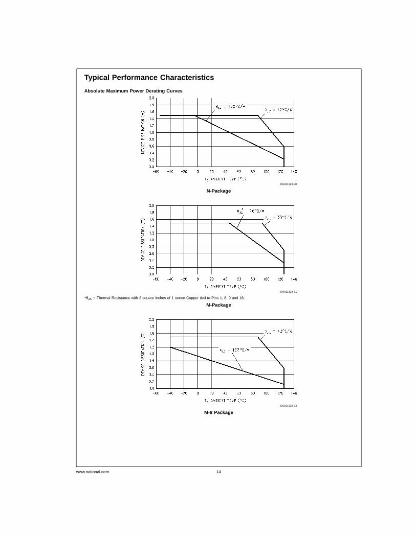
Typical Performance Characteristics
Absolute Maximum Power Derating Curves
DS011328-30
N-Package
DS011328-31
*θJA = Thermal Resistance with 2 square inches of 1 ounce Copper tied to Pins 1, 8, 9 and 16.
M-Package
DS011328-33
M-8 Package
www.national.com 14

Typical Performance Characteristics (Continued)
Simplified Schematic
DS011328-32
www.national.com15
Typical Applications
CURRENT FEEDBACK TOPOLOGY
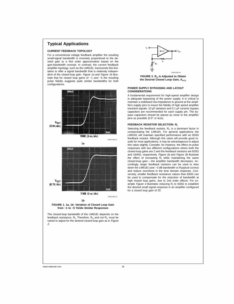
For a conventional voltage feedback amplifier the resultingsmall-signal bandwidth is inversely proportional to the de-sired gain to a first order approximation based on thegain-bandwidth concept. In contrast, the current feedbackamplifier topology, such as the LM6181, transcends this limi-tation to offer a signal bandwidth that is relatively indepen-dent of the closed-loop gain. Figure 1a and Figure 1b illus-trate that for closed loop gains of −1 and −5 the resultingpulse fidelity suggests quite similar bandwidths for bothconfigurations.
The closed-loop bandwidth of the LM6181 depends on thefeedback resistance, Rf. Therefore, RS and not Rf, must bevaried to adjust for the desired closed-loop gain as in Figure2.
POWER SUPPLY BYPASSING AND LAYOUTCONSIDERATIONS
A fundamental requirement for high-speed amplifier designis adequate bypassing of the power supply. It is critical tomaintain a wideband low-impedance to ground at the ampli-fiers supply pins to insure the fidelity of high speed amplifiertransient signals. 10 µF tantalum and 0.1 µF ceramic bypasscapacitors are recommended for each supply pin. The by-pass capacitors should be placed as close to the amplifierpins as possible (0.5" or less).
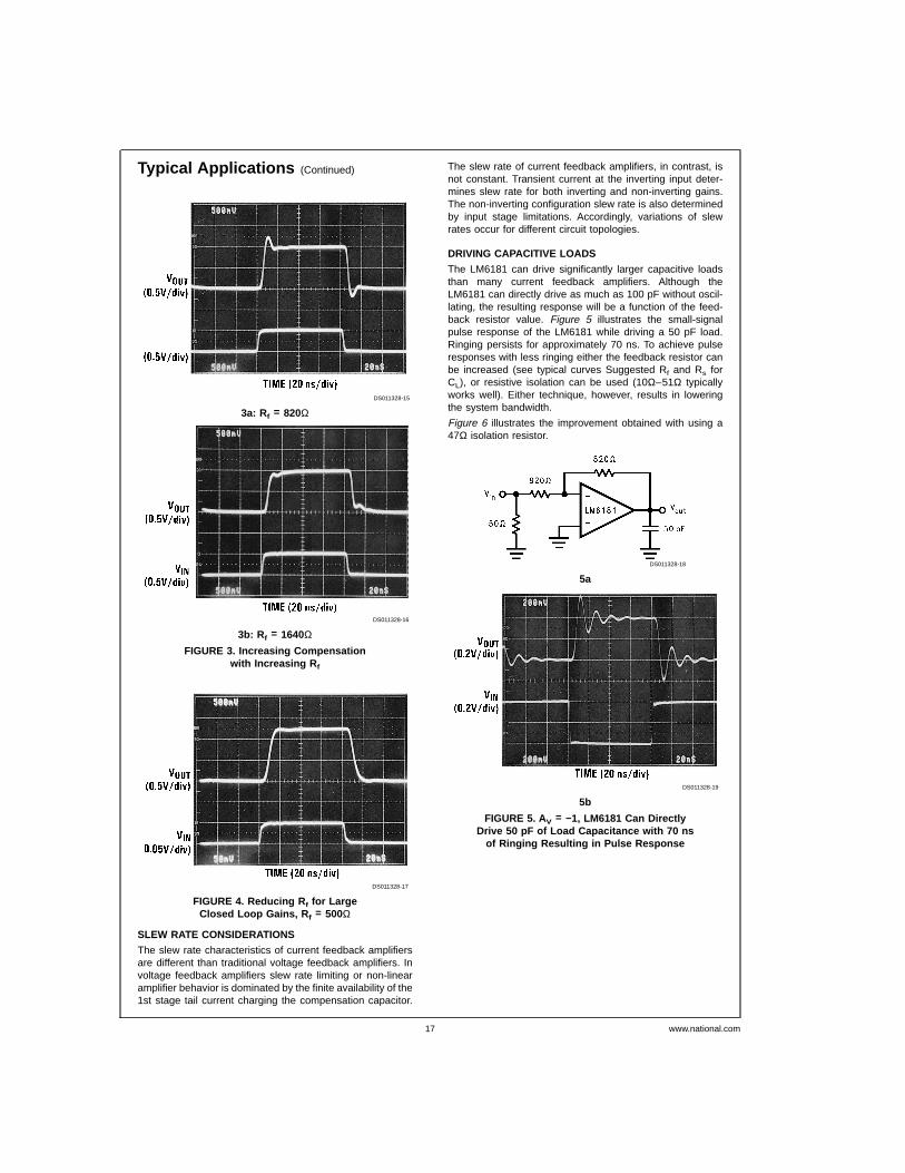
FEEDBACK RESISTOR SELECTION: R f
Selecting the feedback resistor, Rf, is a dominant factor incompensating the LM6181. For general applications theLM6181 will maintain specified performance with an 820Ωfeedback resistor. Although this value will provide good re-sults for most applications, it may be advantageous to adjustthis value slightly. Consider, for instance, the effect on pulseresponses with two different configurations where both theclosed-loop gains are 2 and the feedback resistors are 820Ωand 1640Ω, respectively. Figure 3a and Figure 3b illustratethe effect of increasing Rf while maintaining the sameclosed-loop gain — the amplifier bandwidth decreases. Ac-cordingly, larger feedback resistors can be used to slowdown the LM6181 (see −3 dB bandwidth vs Rftypical curves)and reduce overshoot in the time domain response. Con-versely, smaller feedback resistance values than 820Ω canbe used to compensate for the reduction of bandwidth athigh closed loop gains, due to 2nd order effects. For ex-ample Figure 4 illustrates reducing Rf to 500Ω to establishthe desired small signal response in an amplifier configuredfor a closed loop gain of 25.
DS011328-12
1a
DS011328-13
1b
FIGURE 1. 1a, 1b: Variation of Closed Loop Gainfrom −1 to −5 Yields Similar Responses
DS011328-14
FIGURE 2. RS Is Adjusted to Obtainthe Desired Closed Loop Gain, A VCL
www.national.com 16
Typical Applications (Continued)
SLEW RATE CONSIDERATIONS
The slew rate characteristics of current feedback amplifiersare different than traditional voltage feedback amplifiers. Involtage feedback amplifiers slew rate limiting or non-linearamplifier behavior is dominated by the finite availability of the1st stage tail current charging the compensation capacitor.
The slew rate of current feedback amplifiers, in contrast, isnot constant. Transient current at the inverting input deter-mines slew rate for both inverting and non-inverting gains.The non-inverting configuration slew rate is also determinedby input stage limitations. Accordingly, variations of slewrates occur for different circuit topologies.
DRIVING CAPACITIVE LOADS
The LM6181 can drive significantly larger capacitive loadsthan many current feedback amplifiers. Although theLM6181 can directly drive as much as 100 pF without oscil-lating, the resulting response will be a function of the feed-back resistor value. Figure 5 illustrates the small-signalpulse response of the LM6181 while driving a 50 pF load.Ringing persists for approximately 70 ns. To achieve pulseresponses with less ringing either the feedback resistor canbe increased (see typical curves Suggested Rf and Rs forCL), or resistive isolation can be used (10Ω–51Ω typicallyworks well). Either technique, however, results in loweringthe system bandwidth.
Figure 6 illustrates the improvement obtained with using a47Ω isolation resistor.
DS011328-15
3a: Rf = 820Ω
DS011328-16
3b: Rf = 1640ΩFIGURE 3. Increasing Compensation
with Increasing R f
DS011328-17
FIGURE 4. Reducing R f for LargeClosed Loop Gains, R f = 500Ω
DS011328-18
5a
DS011328-19
5b
FIGURE 5. AV = −1, LM6181 Can DirectlyDrive 50 pF of Load Capacitance with 70 ns
of Ringing Resulting in Pulse Response
www.national.com17
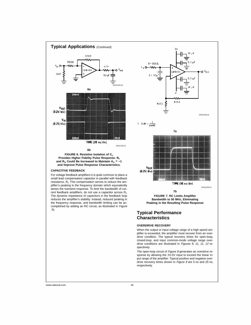
Typical Applications (Continued)
CAPACITIVE FEEDBACK
For voltage feedback amplifiers it is quite common to place asmall lead compensation capacitor in parallel with feedbackresistance, Rf. This compensation serves to reduce the am-plifier’s peaking in the frequency domain which equivalentlytames the transient response. To limit the bandwidth of cur-rent feedback amplifiers, do not use a capacitor across Rf.The dynamic impedance of capacitors in the feedback loopreduces the amplifier’s stability. Instead, reduced peaking inthe frequency response, and bandwidth limiting can be ac-complished by adding an RC circuit, as illustrated in Figure7b.
Typical PerformanceCharacteristics
OVERDRIVE RECOVERY
When the output or input voltage range of a high speed am-plifier is exceeded, the amplifier must recover from an over-drive condition. The typical recovery times for open-loop,closed-loop, and input common-mode voltage range over-drive conditions are illustrated in Figures 9, 11, 11, 12 re-spectively.
The open-loop circuit of Figure 8 generates an overdrive re-sponse by allowing the ±0.5V input to exceed the linear in-put range of the amplifier. Typical positive and negative over-drive recovery times shown in Figure 9 are 5 ns and 25 ns,respectively.
DS011328-20
6a
DS011328-21
6b
FIGURE 6. Resistive Isolation of C L
Provides Higher Fidelity Pulse Response. R f
and RS Could Be Increased to Maintain A V = −1and Improve Pulse Response Characteristics.
DS011328-22
7a
DS011328-23
7b
FIGURE 7. RC Limits AmplifierBandwidth to 50 MHz, Eliminating
Peaking in the Resulting Pulse Response
www.national.com 18
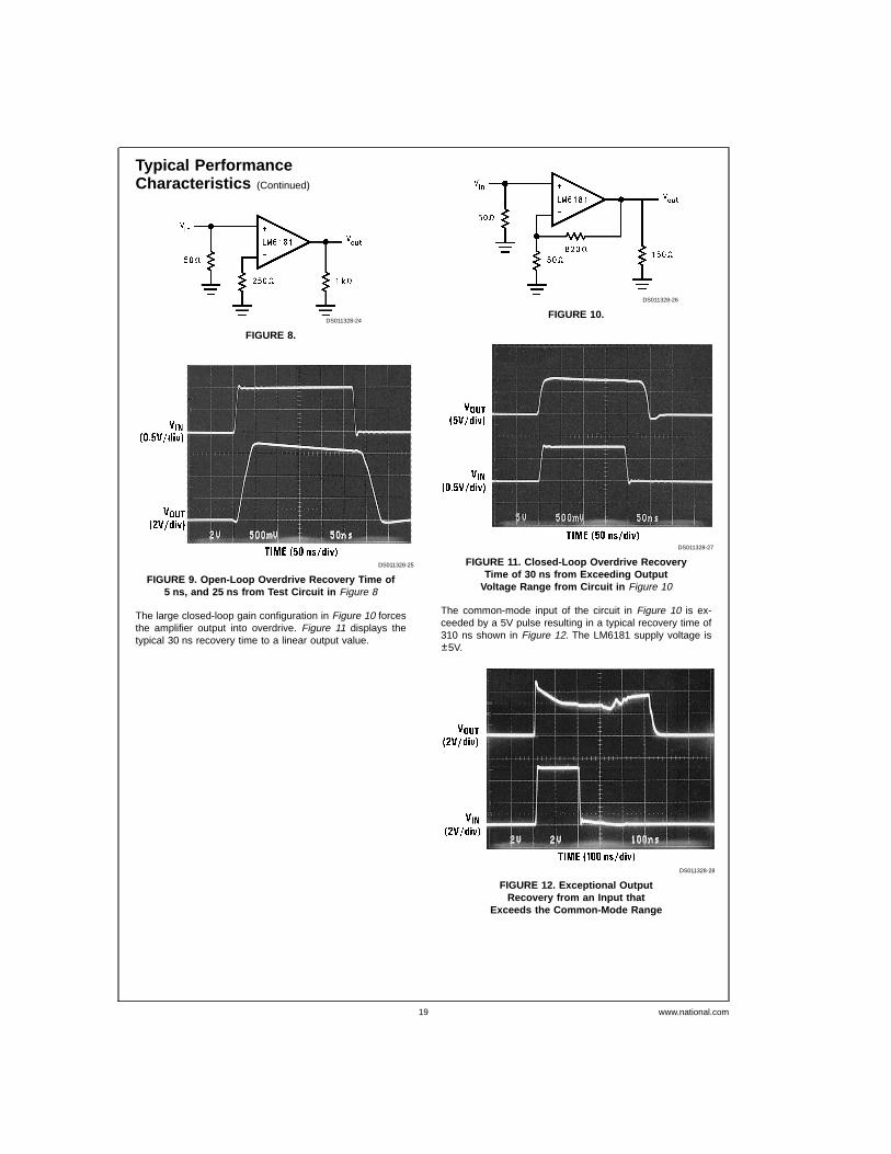
Typical PerformanceCharacteristics (Continued)
The large closed-loop gain configuration in Figure 10 forcesthe amplifier output into overdrive. Figure 11 displays thetypical 30 ns recovery time to a linear output value.
The common-mode input of the circuit in Figure 10 is ex-ceeded by a 5V pulse resulting in a typical recovery time of310 ns shown in Figure 12. The LM6181 supply voltage is±5V.
DS011328-24
FIGURE 8.
DS011328-25
FIGURE 9. Open-Loop Overdrive Recovery Time of5 ns, and 25 ns from Test Circuit in Figure 8
DS011328-26
FIGURE 10.
DS011328-27
FIGURE 11. Closed-Loop Overdrive RecoveryTime of 30 ns from Exceeding Output
Voltage Range from Circuit in Figure 10
DS011328-28
FIGURE 12. Exceptional OutputRecovery from an Input that
Exceeds the Common-Mode Range
www.national.com19
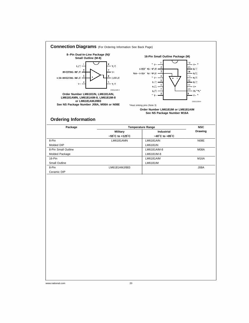
Connection Diagrams (For Ordering Information See Back Page)
Ordering Information
Package Temperature Range NSCDrawingMilitary Industrial
−55˚C to +125˚C −40˚C to +85˚C
8-Pin LM6181AMN LM6181AIN N08E
Molded DIP LM6181IN
8-Pin Small Outline LM6181AIM-8 M08A
Molded Package LM6181IM-8
16-Pin LM6181AIM M16A
Small Outline LM6181IM
8-Pin LM6181AMJ/883 J08A
Ceramic DIP
8–Pin Dual-In-Line Package (N)/Small Outline (M-8)
DS011328-3
Order Number LM6181IN, LM6181AIN,LM6181AMN, LM6181AIM-8, LM6181IM-8
or LM6181AMJ/883See NS Package Number J08A, M08A or N08E
16-Pin Small Outline Package (M)
DS011328-4
*Heat sinking pins (Note 3)
Order Number LM6181IM or LM6181AIMSee NS Package Number M16A
www.national.com 20
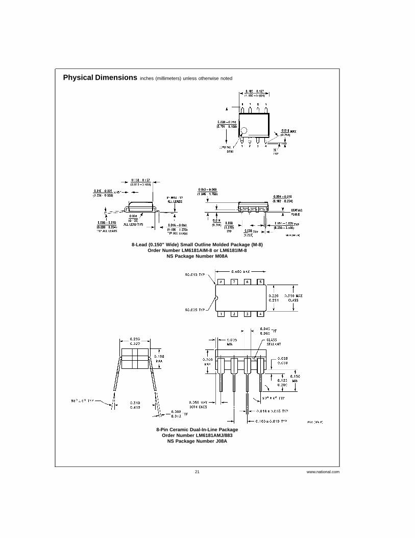
Physical Dimensions inches (millimeters) unless otherwise noted
8-Lead (0.150" Wide) Small Outline Molded Package (M-8)Order Number LM6181AIM-8 or LM6181IM-8
NS Package Number M08A
8-Pin Ceramic Dual-In-Line PackageOrder Number LM6181AMJ/883
NS Package Number J08A
www.national.com21
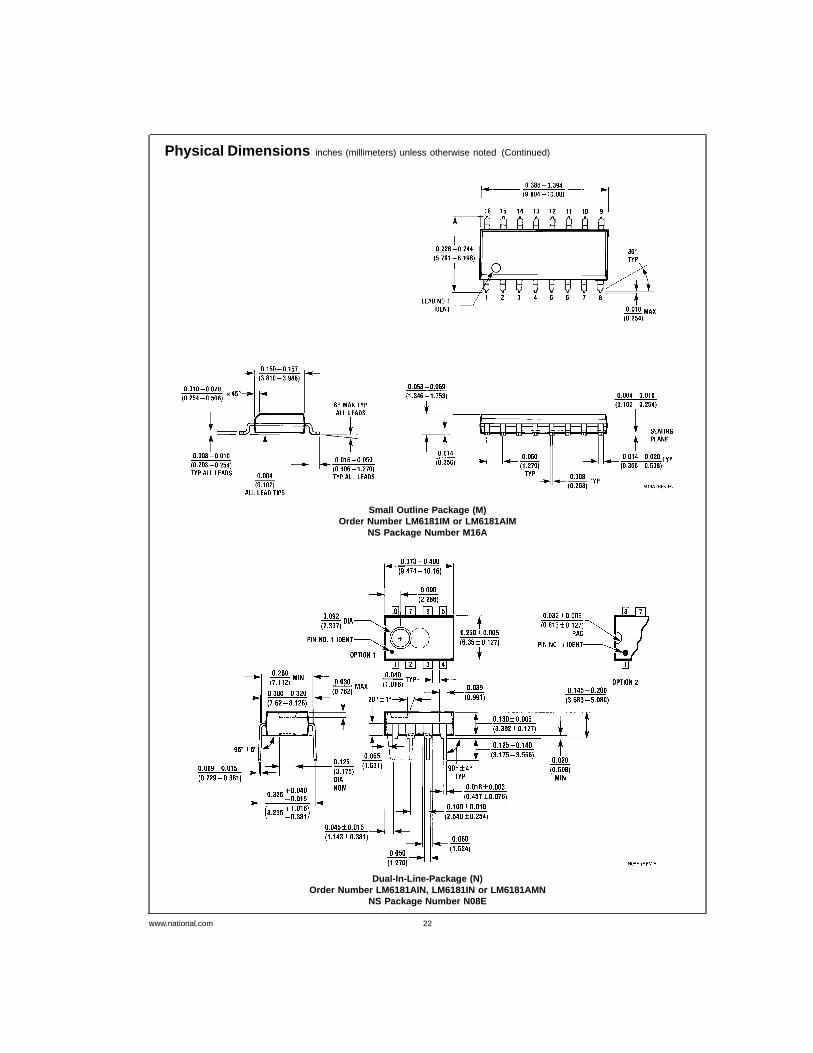
Physical Dimensions inches (millimeters) unless otherwise noted (Continued)
Small Outline Package (M)Order Number LM6181IM or LM6181AIM
NS Package Number M16A
Dual-In-Line-Package (N)Order Number LM6181AIN, LM6181IN or LM6181AMN
NS Package Number N08E
www.national.com 22
Physical Dimensions inches (millimeters) unless otherwise noted (Continued)
LIFE SUPPORT POLICY
NATIONAL’S PRODUCTS ARE NOT AUTHORIZED FOR USE AS CRITICAL COMPONENTS IN LIFE SUPPORTDEVICES OR SYSTEMS WITHOUT THE EXPRESS WRITTEN APPROVAL OF THE PRESIDENT OF NATIONALSEMICONDUCTOR CORPORATION. As used herein:
1. Life support devices or systems are devices orsystems which, (a) are intended for surgical implantinto the body, or (b) support or sustain life, andwhose failure to perform when properly used inaccordance with instructions for use provided in thelabeling, can be reasonably expected to result in asignificant injury to the user.
2. A critical component is any component of a lifesupport device or system whose failure to performcan be reasonably expected to cause the failure ofthe life support device or system, or to affect itssafety or effectiveness.
National SemiconductorCorporationAmericasTel: 1-800-272-9959Fax: 1-800-737-7018Email: [email protected]
National SemiconductorEurope
Fax: +49 (0) 1 80-530 85 86Email: [email protected]
Deutsch Tel: +49 (0) 1 80-530 85 85English Tel: +49 (0) 1 80-532 78 32Français Tel: +49 (0) 1 80-532 93 58Italiano Tel: +49 (0) 1 80-534 16 80
National SemiconductorAsia Pacific CustomerResponse GroupTel: 65-2544466Fax: 65-2504466Email: [email protected]
National SemiconductorJapan Ltd.Tel: 81-3-5639-7560Fax: 81-3-5639-7507
www.national.com
LM6181
100m
A,100
MH
zC
urrentFeedbackA
mplifier
National does not assume any responsibility for use of any circuitry described, no circuit patent licenses are implied and National reserves the right at any time without notice to change said circuitry and specifications.


