
INPUT 1 OUTPUT HARMONIC FREE CURRENT LINK THREE-PHASE AC POWER SUPPLY
Hamid Reza Karshenas
A thesis submitted in conformity with the requirements for the degree of Doctor of Philosophy
Department of Elecmcal and Cornputer Engineering University of Toronto
O Copyright by Hamid Reza Karshenas 1997

National Library I * m of Canada Bibliothèque nationale du Canada
Acquisitions and Acquisitions et Bibliographie Services services bibliographiques
395 Wellington Street 395, nie Wellington OttawaON K1AON4 OttawaON K1A ON4 Canada Canada
Your Ne Votre f f f m C B
Our fi& Noire relerence
The author has granted a non- exclusive Licence allowing the National Library of Canada to reproduce, loan, distribute or sell copies of this thesis in microfom, paper or electronic formats.
The author retains ownership of the copyright in this thesis. Neither the thesis nor substantial extracts fiom it may be printed or otherwise reproduced without the author's permission.
L'auteur a accordé une licence non exclusive permettant à la Bibliothèque nationale du Canada de reproduire, prêter, distribuer ou vendre des copies de cette thèse sous la forme de microfichelfilm, de reproduction sur papier ou sur format électronique.
L'auteur conserve la propriété du droit d'auteur qui protège cette thèse. Ni la thèse ni des extraits substantiels de celle-ci ne doivent être imprimés ou autrement reproduits sans son autorisation.

IN THE NAME OF GOD, THE BENEFICENT, THE MERCIFUL.

To my parents, m y wife,
and my son.
iii

INPUT 1 OUTPUT HARMONIC FREE CURRENT LINK
THREE-PHASE AC POWER SUPPLY
A Thesis for the Degree of Ph.D., 1997
Hamid Reza Karshenas Department of Electrical and Cornputer Engineering
University of Toronto
ABSTRACT
The three-phase current link AC to AC power supply. a relatively new topolog for AC
power supply application, has severai potentiai advantages such as srnalIer nurnber of
magnetic components, lower switching frequency and more rugged operation. Despite this.
i t has received very Iittle attention by the researchers, and the rnajority of work found in the
Iiterature is confined to the application of voltage type converten in this area.
This thesis presents a cornprehensive systematic approach for sready state/dynamic
analysis and design of diree-phase current link AC to AC power supplies.
Concept of P W methods in three-phase current type converters (CTC) is explainrd
and the associated constraints in PWM pattern generation are addressed. Szvercil P W
techniques are described and their performance from different aspects are compared.
A steady state analysis is presented based on the Fourier representation of P W
waveforms which dlows an accurate prediction of the relationships benveen the
fui~dament~larmonic components of the waveforms and other systcm parameters.
Expressions governing various steady state characteristics of the system are denved.

A dynamic model using the concept of local average of signals is established. The
agreement between the dynamic behavior of switching system and derived model is
illustrated. Phenornenon of multiple crossing is explained and the necessary requirement for
avoiding such a phenornenon is obtained. The concept of intemal model controllers is
introduced and its application in the inverter control system for achieving zero steady state
error is descnbed.
A detailed design procedure is presented. Root-locus method is used to design the
system controllers. The applicability of different rnodels in different design problems is
discussed. All s-domain designs are venfied by tirne-domain simulations.
Expenments are conducted on a 2 KVA. 60 Hz to 50 Hz power supply. A 32 bit DSP-
base nigh performance controller is used to implement the control system. The predicted
steady state and dynarnic resuits as well as the time-domain simulations are experimentally
verified.

Acknowledgments
1 wish to express rny deep gratitude to Prof. Shashi B. Dewan. my thesis supervisor. for
his invaluable guidance and suppon. His insight, intuition and supervision helped me to
make my work with him a most gratifying and constnictive experience.
My special thanks go to the rnembers of my Ph-D. defense cornmittee. Professors ;M.R.
Iravani, R. Bonert, R. Pankaj, P. Jain and D.E. Cormack.
1 wish to thank my fellow graduate students at the Power Group for their helpful
discussions and suggestions.
Financial süpport by the [ranian Ministry of Culture and Higher Education and the
National Science and Engineering Research Council (NSERC) of Canada is acknowledged. I
also would like to thank my supervisor for his financial assistance.
1 am wholly indebted to my parents in Iran for their sincere. endless and pure love and
affection. They have always given me their generous support and encouragement. and
always inspired me to set my goals high. 1 can never thank them enough for al1 the values
they have bestowed upon me.
The last but certainly not the least, 1 have a great debt of gratitude to express towards
my wife, Maryarn, for her intense care and devotion. Without her understanding and support.
this work wouldn't have been possible.

TABLE OF CONTENTS
ABSTRACT
ACKNOWLEDGMENT
TABLE OF CONTENTS
LIST OF SYMBOLS
Chapter 1 INTRODUCTION
1.1 Currently Available AC to AC Power Supplies
1.2 S inusoidal Input/Output Power Suppl y
1.2.1 Direct AC to AC Power Supply
1.2.2 Voltage Type AC to AC Power Supply
1.2.3 Current Type AC to AC Power Supply
1.2.4 Cornparison
1.3 Description of the Proposed System
1.4 Thesis Objectives
1.5 Thesis Outline
Chapter 2 SYSTEM DESCRIPTION
2.1 System Structure
2.1.1 System Block Diagram
2.1.1 Power Circuit Structure
i v
vi
vii
xii

2.1.3 Experimental Setup 2.6
2.2 Concepts of Pulse-width Modulation in CTC 2.9
2.2.1 PWM Pattern Generation constraints in CTC 2.1 1.
2.2.2 Basic Definitions 2.13
2.2.3 Selected Harmonic Elirnination PWM (SHE-PWM) Method 1.15
2.2.4 Space Vector PWM ( S V - P m ) Method 2.16
2.2.5 Sinusoïdal PWM (SIN-PWM) Method 2.20
2.2.6 Cornparison and Selection 2.25
2.3 Basic System Operation 2.28
2.4 Operation Under Unbalanced and Nonlinear Loads 2.3 1
Chapter 3 STEADY STATE ANALYSIS OF A CURRENT LINK AC TO .AC
P O W R SUPPLY
3.1 Basic Assumptions
3.2 Rectifier Steady State Analysis
3.2.1 S teady State Modeling
3.2.2 Unity Power Factor Operation
3.2.3 Input Filter Analysis
3.2.4 Component Rating
3.3 Inverter Steady State Analysis
3.1. t Steady S tate Modeiing
3.3.2 Relationship Between Fundamental Quantities
3.3.3 Output Filter Analysis
3.3.4 DC Current Amplitude
viii

3.3.5 Component Rating
3.4 Intermediate DC Link
3.4.1 S teady State Modeling
3.4.2 Basic AUDC Relationships
3.4.2.1 Fundamental A U D C Relationship
3.4.3 Harmonic and DC Filter Analysis
3.5 Theoretical and Expenmentai Verifications
3.6 Input/Output Relationship as an AC CO AC Power Supply
Chapter 4 DYNAMIC ANALYSIS OF A CURRENT LINK AC TO AC
P O W R SUPPLY
4.1 Simplifjhg Assumptions
4.2 Averaging Technique For Modeling S wi tc hing Circuits
4.2.1 Concept Of Local Average of Signals
4.2.2 Modeling of the Basic Switching Function Generator
4.3 Rectifier Dynamic Analysis
4.3.1 Rectifier Dynamic Modeling
4.3.2 Rectifier Control Strategy
4.3.3 Closed Loop Gain Considerations
4.4 Inverter Dynamic Analysis
4.4.1 Inverter Dynamic ModeIing
4.4.2 Inverter Control System Structure and Strategy
4.4.2.1 Concept of Intemal Model in Control systems
4.4.3 Gain Calculation and Multiple Crossing Phenornenon

4.5 Interpretation of Systern Bandwidth
4.6 Control S ystem Decoupling
4.7 IlIustrative Example
4.7.1 System Description
4.7.2 Dynamic Performance
4.7.3 Modeling Verification
4.7.4 Interna1 Mode1 Versus PI Controller
4.7.5 Multiple Crossing Phenornenon
4.8 Experimental Verification
Chapter 5 DESIGN OF A'CURRENT LINK AC TO AC POWER SUPPLY
5.1 Design Criteria 5.2
5.2 Design Procedure 5.3
5.2.1 Calculation of Steady State Parameters
5.2.2 Controller Design
5.2.3 Time Domain Simulation
5.3 Design Example 1
5.3.1 Calculation of Steady State Parameters
5.3.2 Controller Design
5.3.3 Time Domain Simulation
5.4 Design Example 2: Experimentai System Design
5.4.1 Calculation of Steady State Parameters
5.4.2 Controller Design
5.4.3 Time Domain Simulation

Chapter 6 CONCLUSION
REFERENCES
APPENDIX

LIST OF SYMBOLS
In this thesis, lower-case letters normally refer CO instantaneous quantities and the
upper-case letters to constants or rms values. Also. bar notation refers to local average of
signals and hat notation refers the peak value of quanrities. Characters in boid print refer to
phasor or space vector quantities.
General Subscripts
i
n
I
max
O
S
A
three phase quantities.
transformed two phase quantities.
ms value of variables.
DC value of variables or variables corresponding to intermediate DC Iink.
base value of corresponding variable.
variables corresponding to the rectifier.
variables corresponding to the inverter.
nth harmonic cornponent
fundamentai component.
maximum value.
denoting values corresponding to system output, Le. load side.
denoting values corresponding to input supply.
denoting peak value of signals.
xii

Voltages
Currents
rectifier input voltage across filter capacitor.
supply voltage.
rectifier output voltaa.
inverter input voltage.
output voltage across filter capacitor.
reference voltage.
modulating signal (aiso expressed by m).
carrier signal.
phase voltages.
line voltages.
phase voltage.
Iine voltage.
peak value of modulating signal.
peak value of carrier signal.
rectifier input (P WM) current.
supply current.
intennediate DC current.
inverter output (PWM) current.
output (load) current.
filter capacitor current.

iM magnetizing current of isolating transformer.
lriPple ripple current in intermediate link.
te-,P current template.
if total output dlter current ( including capacitor and magnetizing inductor).
I . current reference.
Control Variables
e error signal.
u controller output signaI.
rn rnodulating signal.
Circuit Components
L , input filter inductance.
Cr input filter capacitance.
LDC inductance of intermediate DC filter.
R~~ resistance of intermediate DC filter.
ci output filter capacitance.
LM magnetizing inductance of isolating transformer.
4 load inductance.
RI Ioad resistance.
xiv

Frequencies, Tirne and Time Constants
frequency (radian Vsecond).
fundamental frequency.
carrier frequency.
switching frequency.
sarnpling frequency.
times associated with SV-PWM pattern generation.
time constant of the rectifier PI controller.
time constant of the inverter PI controller.
Gains, Constants and Coefficients
N number of hmonics to be eIiminated.
Kpv Kv, K, coefficients for perunit base transformation.
K.s simplifying constant (rectifier steady-state operation).
A k Fourier coefficients of switching function.
Kr rectifier controlier gain.
Ki inverter controller gain.
a09al coefficients of numerator of inverter controller.
~ 1 ~ ~ 2 inverter controller zeros.
Transfer Functions
Cr rectifier transfer funetion.
GDC trmsfer function of the intermediate DC link.

Gi inverter transfer function (including filter and load).
6 transfer function of rectifier controller.
Hi transfer function of inverter controller.
Hf transfer function of the output filter.
Mransfer function introduced by phase decouplinp.
Miscellaneous
THD total hmonic disronion.
S switching hinction.
m and M modulation index.
mf frequency modulation ratio.
Y angle between PWM current and voltage.
0 angle between filtered current and voltage.
D distortion factor.

CHAPTER 1
INTRODUCTION
Fixed frequency power supplies are mainly used when the frequency of existing .AC
source is different from the frequency required by the load. Major applications of such sys-
tems are in remote power supplies with high-speed high-frequency generators. off-board test-
ing of aircraft power supplies, marine power supplies. windmill generators. etc. Research
work reported in this area in the literature is mainly confined t o the application of voltage
source inverters (VST). The application of current link configuration in such systems. on the
other hand, has received very littie attention in the literature. This thesis is primarily con-
cemed with steady-state/dynarnic analysis and design of a current link AC to AC power sup-
ply and its implementation with a high performance DSP-based digital controller.
The conventional fixed frequency AC to AC power supplies employ diode or phase
controlled rectifiers as the front end converter. This results in injection of substantial har-
monics into the supply grid, which in tum leads to voltage distortion throughout power grid
because of the finite impedance of distribution systerns. This is not desirable since power
systems generally have harmonic sensitive loads. Furthemore, in case of using front end
phase controlled rectifiers, the system has poor power factor at light loads which increases
reactive power requirement. Therefore, the demand for drawing sinusoidai near unity power
factor current from the network is currently becoMng more stringent [l]. On the other hand.
a power supply must have a fast transient response and reliable operation. Again. it is

difficult to meet these requirements in the conventional fixed frequency power supplies.
The research done in this thesis work is intended to minirnize the above mentioned
problems by proposing a three-phase fixed frequency AC to AC power supply with .
sinusoidal input/output current. The topology adopted for the proposed system is based on
indirect frequency conversion schernes with intermediare DC current link. in which the
energy is fint transferred into the intermediate DC current link and then to the load. With
such a stmcnire, the folIowing features cm be achieved:
Neither input nor output filter needs an inductor.
Since the current is basically conuolled by the front end rectifier, the inverter stage can
operate with lower switching frequency. This increases the potential for medium and
high power applications.
The system is inherently more reliable since the current is controlled and limited by the
front end stage.
Difference between on-state switch voltage drops does not cause imbalance andor DC
component at the output voltage.
As mentioned above, such a configuration has not been investigated in the literature as a
fixed frequency AC to AC power supply, and hence its potential advantages have not been
hilly explored. This is the main motivation for conducting a comprehensive study for
steady-state/dynamic analysis and design of such a system. Further, the analysis presented in
this thesis is verified by:
( I ) time-domain simulations, and
(2) an experimental 2 KVA laboratory set-up with a 32 bit DSP-based digital controller.
In this chapter, the structure of currently available AC to AC power dong with associ-
ated problems are described. The qualitative requirements for an AC to AC power supply
with sinusoidal inputloutput current are mentioned. Some proposed schemes for achieving

such requirements are bnefly described and compared. The potential advantages of the pro-
posed system are explained and its block diagram is described. The objectives and outline of
this thesis conclude this c hapter.
1.1. Currently Available AC to AC Power Supplies
The structure of a conventional three-phase static AC io AC power supplies is shown in
Fig. I.1.a. The front end stage which is a diode or phase controlled rectifier has the following
disadvantages:
0 The input current contains low frequency harmonics with significant amplitude which are
difficult to filter out. The current harmonics lead to voltage harmonics in the power system
which is undesirable for many sensitive loads in the input power supply.
a In phase controlled rectifiers, the system operates with poor power factor at light loads
which increases the reactive power demand of the system.
a In case of need for intermediate DC voltage control. the transient response is relatively
slow.
The inverter is a pulse-width modulated Voltage Source Invener (VSI) which is the
rnost established scheme both in the Iiterature and market. The inverter switching cells con-
sist of a unidirectional controlled switch plus an anti-parallel diode. as shown in Fig. 1.l.b.
The voltage regulation in such systems is norrndly achieved-by an average voltage control
scheme and the overcurrent protection is performed by current trip feature, i.e., the gating
signals are disabled in case of overcurrent. The existing problems with the inverter section
are as follows:

Figure 1.1. (a) Power circuit structure of a conventionai AC to AC power supply with front end diode rectifier and (b) typical switch realization.
*The voltage regulation scheme is inherently sluggish due to a low pass filter normally
employed in the feedback path. This. in ~ r n , results in a poor transient performance dur-
ing disturbances. Moreover, slow transient response normally causes high peak current
during transients.
a The overcurrent protection strategy normally results in total system shutdown. Further. the
system recovery is slow. Tnerefore. the system is not fault-tolerated, i.e.. it cannot ride
through disturbances.
8 Any imbalance in the PWM patterns or forward switch drop causes DC component at the
output voltage. This component can increase the magnetizing current of transfomers at

the load side,
a Voltage imbalance occurs during unbalanced loads.
Therefore, the cunently available power supplies do not meet the performance
specifications of a high quality AC to AC power supply with sinusoidal input/output current.
1.2. Sinusoidal Input/Output Power Supply
The qualitative performance specifications for a fixed frequency AC to AC power sup-
ply with sinusoidal input /output current are the following:
0 Satisfactory steady-state characteristic such as low distortion and balanced output voltages
during al1 operating conditions, low distonion n e z unity power factor input current. and
voltage and frequency stability.
a Fast transient response and minimum distonion in case of load disturbances.
0 Reliable performance and self protection.
In sumrnary, the system must function as an ideal AC voltage source when seen from
the load side, and as a resistive load when seen from the input side.
The above requirements are the main motivations to propose an AC to AC converter
with low distortion near unity power factor input current and high quality output voltage.
With the current and prospective power electronics technology, the following schemes c m
be proposed to realize such a system:
(1) Direct AC to AC converters, dso known as Force Commutated Cycloconverten (FCC)
or Ventunni Converter or Matrix Converter [3,4,5] in the Iiterature; in which the input
and output lines are directly connected together by a properly operated set of switches.

(2) Indirect AC to AC converters with front end PWM rectifiers and
(3) Indirect AC to AC converters with front end active filter.
Indirect PWM converters are also grouped into two major categories:
( 1) Indirect converters with intermediate voltage link and
(2) indirect converters with intermediate current link.
Traditionally, inverters with input DC current are called current source inverter (CSI).
primarily because they hinction as an AC current source as seen from the load side. In the
proposed system, on the other hand, the inverter is characterized by a voltage source as seen
from the load side, and yet has a DC current input. Therefore. it is called current type
inverter (m. Consequently, the front end rectifier which has the sarne structure is called
current type rectifier (CTR). For consistency, voltage source inverterhectifier (VSYR) is also
termed voltage type inverterlrectifier (VTVR).
1.2.1. Direct AC to AC Power Supply
The structure of a direct AC to AC power supply with associated filter components is
shown in Fig. 1.2.a. The input and output filters are the inûinsic part of the circuit and neces-
sary for proper circuit operation. Each switching cel; in this structure must be a bidirectional
switch with the capability of voltage blocking in both directions. An example of practical
implementation of such a switch using hsulated Gate Bipolar Transistors (IGBT) is shown
in Fig. 1.2.b. Based on this figure, 18 controlled and 18 uncontrolled switches are required in
this structure. The output voltages and input currents are synthesized by proper selection of
conducting switches. The ratio of output/input voltage is inainsically limited to f i l 2 [ 5 ] .
There is no published literature regarding the performance investigation of a direct AC
to AC power supply. However, the following problems associated with this scheme cm be

Figure 1.2. (a) Power circuit stmcnire of a direct AC to AC converter and (b) typical switch redization.

recognized from the existing iiterature:
The switch count is high.
r The realization of bidirectional switches suffen from practical difficuities such as gate -
drive isolation and high dvldt blocking requirement[S].
0 The ratio of outputlinput voltage is intrinsically [imited to i%2. resulting in low switch
utilization.
rn The PWM generation schemes in these converters are more complicated than those in
other systems, and small timing inaccuracies Iead CO uncharacteristic hmonics and DC
component ar both sides. Moreover. the input/output harmonics affect each other. i.e. the
inherent decoupling effect of indirect conversion schemes does not present in direct
schemes.
1.2.2. Voltage Type AC to AC Power Supply
The stmcture of a voltage type AC to AC power supply with sinusoidal inputIoutput
current using a PWM rectifier at the front end is shown in Fig. 1.3.
To eliminate the input current distortion and achieve unity power factor operation. a
voltage type PWM rectifier (VTR) is employed as the front end rectifier. This scheme is also
known as voltage source converter or boost PWM rectifier or synchrono~s rectifier [6,7.8].
The power circuit structure and switch requirements of the rectifier are sirnilar to those of the
inverter. The inductors at the input terminal are an intrinsic part of the circuit and necessary
for system opention.
A voltage type rectifier (VTR) always requires closed loop control for proper operation.
Further, because of the susceptibility to input line disturbances, this control has to be fast and
precise. The performance of this rectifier resembles boost converters. i.e. the output voltage
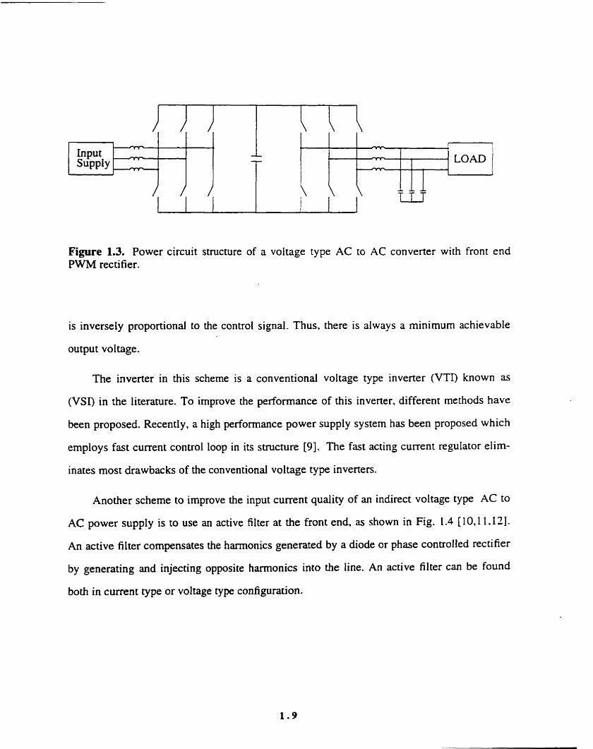
Figure 1.3. Power circuit structure of a voltage type AC ta AC converter with front end PWM rectifier.
is inversely proportional to the control signal. Thus. there is always a minimum achievable
output voltage.
The inverter in this scheme is a conventional voltage type inverter (VTI) known as
(VSI) in the literanire. To improve the performance of this inverter. different methods have
been proposed. Recently, a high performance power supply system has been proposed which
employs fast current control loop in its structure [9] . The fast acting current regulator elim-
inates most drawbacks of the conventional voltage type inverters.
Another scheme to improve the input current quality of an indirect voltage type AC to
AC power supply is to use an active filter at the front end, as shown in Fig. 1.4 [IO. 1 1.121.
An active filter compensates the harmonics generated by a diode or phase controlled rectifier
by generating and injecting opposite harmonics into the line. An active filter can be found
both in current type or voltage type configuration.

- INPUT SUPPLY
ACTIVE FlLTER
Figure 1.4. Power circuit structure of a voltage type AC to AC converter with front end ac- tive filter.
1.2.3. Current Type AC to AC Power Supply
The structure of a current type AC to AC power supply is illustrated in Fig. 1 S.3 [39].
As can be seen, the rectifier and inverter have sirnikir power circuit structures. The switch-
ing cells are unidirectional for current conduction with reverse voltage blocking capability.
Typical realization of such a switch is shown in Fig. 1.5.b. The capaciton at the inputloutput
terminais absorb current harmonics and also suppress the voltage spikes caused by current .
commutation in inductive parts of circuit.
The front end current type PWM rectifier [13.14] maintains the DC current through the
intermediate link while drawing low distortion unity power factor current from the source.
The input filter is necessary to absorb the high frequency hmonics of the rectifier input
current. This fiker is prone to oscillation caused by uncharacteristic harmonics of the rectifier
input current.
The input DC current is pulse-width modulated by the inverter and converted to PWM
AC currents. The output filter integrates the current pulses to realize the output voltage. The
iündarnentai output voltage is conuolled by controlling the fundamental output current. This
stmcture is more common in AC motor drives, and hence its application and performance as

SUPPLY - I - LOXD 1
Figure 1.5. (a) Power circuit structure of a current type AC to AC converter with front end PWM rectifier ( C m ) and (b) typicd switch reaiization.
a fixed frequency power supply has received very little attention in the literature. As a result.
its advantages and disadvantages are not fully explored.
The active filter solution is not applicable in this structure since the rectifier output vol-
tage has to be controlled in a fast manner in order to control the DC current in the link.
13.4. Cornparison
The structure of the proposed AC to AC converters can be found in the literature. How-
ever, their performance as an AC to AC power supply has not been fully investigated. and
dius the cornparison and selection at this stage cannot be made based on their performance.
Therefore, to select one of the proposed systems. the following criteria are taken into

consideration:
( 1) S witching frequency
(2) Switch count
(3) Number and size of magnetic components
(4) Reliability and self protection
Switching frequency is an imponant issue in power electronic systems. It is generally
desirable to shift dominant harmonies of the PWM waveforms to higher frequencies by
employing higher switching frequencies. This reduces the filter size and enhances the
dynamic performance. On the other hand. switching Iosses become the main source of
power dissipation at high switching frequencies and cause system derating. Funher. because
of the stray inductances in the circuit layout. fast switching normally causes substantial
overshoots across switches during turn odoff instants. Unless properly darnped. these
ovenhoots degrade the switch performance. This phenornenon becomes more noticeable in
high power applicat~ons where the current rating is hjgh.
n i e current regulation scheme in the high performance VTI [9] needs a relatively high
switching frequency for adequate performance. This requirement is not so stringent in CTI.
as the current regulation is performed in the front end rectifier. Therefore. for the same per-
formance, lower switching fiequency could be selected in CTC.
The switch count in direct converters is the highest among other structures. The switch
count in voltage type and current type converters is the same. When an active filter is
employed at the front end stage. the switch count would be higher. although the switch rating
in active filter is lower.
The number of magnetic components is important since they are bulky and expensive.
As a matter of fact. with the recent advances in manufacturing high power semiconductors,

magnetic components play a major role in determining the system cost. The number of rnag-
netic components is the highest in a direct voltage type converter. Note again that inductors
both at the input and output tenninals in Fig. 1.2 and Fig. 1.3. are intrinsic pans of the
input/output filters and essentiai in system operation. The current type converter normally
uses oniy one inductor in the DC link. whose size c m be reduced by using high switching
frequencies in the converters. The input fiiter inductance is very small and normaily the
source inductance is satisfactory.
Reliability and robustness are crucial factors in al1 power supply systems. Mrnost d l
proposed methods for improving the performance of a VTI are based on controlling the out-
put (inductor) current in a rapid manner [9]. In other words, the inverter is forced to behave
as a current source. On the other hand, it can be intuitively said that a current type inverter
with inherent current control has dl the features mentioned in [9] without the need for inner
current loop. For instance, over current protection would becorne more straightfonvard and
the system cm sustain faults without total shutdown. Furthemore. overcurrents due to DC
voltage component are eliminated. Protection in direct converters is difficult. particularly
because of the problems in impiementation of bilateral switches [5] .
Table 1.1 sumrnerizes the above cornparison.
1.3. Description of The Proposed System
Figure 1.6 illustrates the block diagram of the proposed system which is composed of
two main subsystems, i.e. a current type PWM rectifier (CTR) and a current type inverter
(0. Two converters have their own control circuits, i-.e. the control systerns are decoupled
as will be explained in Chapter 4.
As already explained, both the inverter and rectifier have the structure of a conventional
three-phase bridge consisting of six self-comrnutated unilateral switches with the capability

Table 1.1. Cornparison of different AC to AC power supplies.
switch 1 magnetic switching protection
Direct Converter
high / n e e d s fast 1 ! switching fre- 1 ! 1 quency 1
!
count' II cornponents frequency'" , feasibiIi~y i I I ! I
1 1
6 i
18 / I high difficult ; 1
voltage type converter with front end PWM rectifier - - - - - - -
i 1 1 60r1'~) 1 t voltage type converter high 1 needs fast 1 with front end active , ; switching fre-
filter I
i i qLIenCy i I
12
( 1 ) Only controlled switches are counted.
current type converter
( 2 ) Switching frequency for the s m e performance.
(3) Depending on the configuration of the active filter. (4) The supply inductance is norrnally sufficient for filter inductance, and thus additional
inductance is not necessary or will be very srnall.
12
of reverse voltage blocking. The capaciton at the AC terminais (Fig. 1.5) absorb high fre-
quency cument and suppress the voltage spikes caused by current commutation in the circuit.
I I medium 1 straightforwardj
I
The system operates with fixed intemediate DC current. The DClAC conversion is per-
formed by means of pulse-width modulation (PWM) techniques. and the amplitude of tünda-
mental quantities is controlled by modulation index control. In this way, there are some con-
cepnial constraints associated with PWM generation techniques in the-phase CTC which
have to be taken into consideration. The employed PWM method is carrier-based sinusoidal
Pw in which the PWM patterns are generated by comparing the modulating (sinusoidd)
signals with a viangular or sawtooth carier waveform.
1 . 14


The inverter control strategy is based on tracking control systems [15]. i.e. the output
voltage is forced to track a sinusoidal reference signal. The output voltage v, is cornpared
with the reference voltage v ' and the error ej is sent to the controller. The controller output
ui which is the sarne as the inverter modulating signal mi is fed to the PWM generatlng block
to generate the proper gating patterns. This signal controls the fundamental output current
which consequently adjusü the fundarnental output voltage. This control strategy dong with
high system bandwidth provides a good dynarnic response for the system. as compared to the
conventionai regulation schemes discussed earlier.
A common problem in tracking control systems with sinusoidal reference signal is the
non-zero steady-state tracking enor. To eliminate this. the concept of interna1 mode1 con-
troiiers is used in the design of inverter control system. that is. the controller structure is
selected to be similar to the structure of the reference signals [16.17].
The rectifier control strategy is based on conventional regulator systems [ 15). The DC
current iDc is compared with the reference current 1' and the error e , is fed to the controller.
The controller output u, is muitipiied by the current template signals i,,, to generate the
modulating signals rn, for the PWM generating block. The amplitude of these signals is such '
that a fixed DC current is maintained in the link, and their phases are adjusted such that near
unity power factor operation is achieved.
Al1 the control and PWM generating blocks shown in Fig. 1.6 are implemented using a
32 bit DSP-based high performance digital controller developed at the Power Group at the
University of Toronto [Hl. The detailed description of this experimental setup is &en in
Chapter 2 and Appendix A.

1.4. Thesis Objectives
The main objective of this thesis is to perform a comprehensive study and expenrnental
verification for steady-state/dynamic analysis and design of a current link AC to AC power
supply with sinusoidal input/ output current. As mentioned in rhe literature review. such a
system has received little attention in the literanire and consequently its performance has not
been fully explored. Therefore. this thesis attempts to provide the basic tools and guidelines
for analysis and design of such a system. to identify its advantages and disadvantages. and to
venfy the analysis by cornparison of theoretical and expenmental resuits. More specitically.
the thesis objectives are as follows:
(1) To identify the existing constraints in generating PWM patterns associated with three-
phase current type converters. Further, to investigate the performance of PWM tech-
niques adaptable for three-phase CTC.
(2) To present a comprehensive steady-state analysis of the system. which includes deriv-
ing relevant expressions for filter design in different stages. obtaining voltage and
current distortion in terrns of system parameters, calculating components rating, and so
on.
(3) To establish an appropriate modeling approach in order to model the nonlinea. switch-
ing converten for proper dynamic analysis. Specifically, such a model should have the
capability of k i n g handled by existing tools for linear conwl systems.
(4) To propose a control strategy in order to achieve al1 steady-state and transient perfor-
mance specifications.
(5) To develop a systematic design procedure based on the steady-state and dynamic ana-
lyses and given performance specifications.

(6) To conduct experiments on
digital controller in order to
a laboratory setup by using a high performance DSP-based
verify the theoretical results.
1.5. Thesis Outline
This thesis consists of six chapters outlined as follows:
In Chapter 2, an overall description of the system is presented. The general structure of
the power circuit is described. The experirnental setup is shown and its block diagram is
described. The concept of PWM rnethods in three-phase current type converters is
explained. Different PWM schemes are explsined and. their performance is compared. The
basic system operation is explained with the help of illusrrative examples.
Chapter 3 presents a detailed steady-state analysis of the system. The bais for this
analysis is representation of PWM waveforms by their Fourier series. The
input/intemediate/output filter anaiysis is camied out based on dominant harmonies of the
PWM waveforms. Various expressions and graphs are provided for filter design. General-
ized expressions between fundamental/harmonic components of ACDC currents and vol-
tages are obtained. Theoretical and experimental verifications are given. The system opera-
tion as an AC voltage booster is explained and discussed.
Chapter 4 presents the dynamic anaiysis of the system. The concept of local average of
signais is introduced and the system modeling is carried out. The control strategy for the
inverter and rectifier is eiaborated. The concept of interna1 rnodel controllers is introduced.
and its application for tracking a sinusoidal signal with zero steady-state error is explained.
The multiple crossing phenornenon and its effect on limiting the closed loop gain is
described. nlustrative examples are presented to provide insight into various aspects of SYS-
tem operation. Theoretical and experimen ta1 verifications are given.

In chapter 5, a systematic design procedure is presented based on the analysis per-
formed in Chapter 3 and 4. Two illustrative design examples are presented to highlight
important aspects of the system design. The design of the experimental system is described.
Chapter 6 presents the thesis conclusions and major contributions.

CHAPTER 2
SYSTEM DESCRIPTION
Introduction
This chapter presents a general description of the indirect AC to AC power supply with
intermediate DC current Iink which was proposed in Chapter 1 . The description includes the
system block diagram, power circuit structure and the experimental set-up. Also. the concept
of PWM methods in three-phase current type conveners is discussed in detail.
Pulse-width Modulation techniques are widely used in power electronic systems [19].
Application of these techniques in three-phase current type converters (CTC). however.
suffers from some restrictions mainly due to the fact that the DC current must not be inter-
rupted in the circuit [20] . In this chapter. the basic requirements for generating PWM pat-
terns in a 3-phase CTC are introduced. Various PWM rnethods are described and their per-
formance is compared. This cornparison is prirnarily based on open-loop and closed-loop
characteristics, switching frequency, low order harmonies etc.
This chapter is organized as follows:
Section 2.1 descnbes the system configuration. The overail system block diagram and
power circuit structure are described. The basic requirernents for power switches are dis-
cussed. The experimental set-up is described and the function of different blocks is briefly
explained. The detailed description of the experimental system is given in Appendix A.

In section 2.2. the concept of pulse-width modulation (PWM) techniques as applied in
current type converters is explained and the associated constraints are addressed. Different
PWM methods are briefly explained and their characteristics are mentioned. The implernen-
tation of carrier-based sinusoidal PWM (SIN-PWM) employed in the proposed system is
described.
Section 2.3 presents the basic system operation. Different illustrative wavefoms in this
section provide better insight into system operation.
In Section 2.4, the system operation with unbalanced and nonlinear load is illustrated.
2.1. System Structure
In this section, an overview of the system structure is presented including the system
block diagram and power circuit structure. Also, the experirnental setup is shown and briefly
described.
2.1.1. System Block Diagram
The overall block diagram of the system is shown in Fig. 2.1. Two major sections can
be recognizeci from this diagram: (1) The front end current type rectifier (CTR) plus inter-
mediate DC link and (2) the voltage controlled current type inverter (CTT). A brief descrip-
tion of each block is presented in the following.
The front end rectifier functions basically as a current regulator to maintain fixed DC
current in the intermediate DC link. It also keeps the input current i, in phase with the input
voltage v, to achieve unity power factor operation. In doing so. the error signal e, between
the output current iDc and the reference current I * is sent to the rectifier controller. The con-
troller output u, is multiplied by the current template ikVT resulting in the rectifier PWM
control signals m,. These signals, after being processed by the PWM pattern generator. gen-
erate the appropriate gating patterns for the rectifier switches. As a result, the output DC
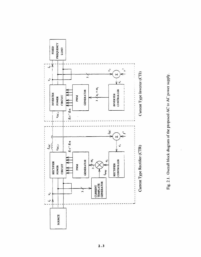

current is regulated. and at the same time the input current remains in phase with the input
voltage.
The hnciion of the inverter is to regulate the output voltage v,. The instantaneous error
signal ei between the output voltage v, and the reference voltage v' is sent to the inverter
controller. The controller directly produces the PWM control sipnals mi for the invener.
These signais are processed in a PWM generator circuit which is basically similar to that of
the rectifier. This block produces appropriate gating patterns for the inverter. which eventu-
ally results in fixed output AC voltage. Since the current is inherently controlled and limited
by the rectifier. there is no need for current control loop in the inverter section.
2.1.2. Power Circuit Structure
The detailed structure of the power circuit is shown in Fig. 2.3.a. Both the rectifier and
inverter have the structure of a conventional three-phase bridge. The ernployed switches in
the circuit must be unidirectional with reverse voltage blocking capability. This means that
they m u t be able to conduct the current in one direction. but withstand the voltage in either
direction .
The inductive nature of DC link does not allow any current interruption in the circuit.
As a result, any uncontrolled open circuit must be avoided in the circuit. Therefore. addi-
tional crowbar switches Sa,, 1 to SaUV 3 are aiso incorporated in the circuit to bypass the DC
current in case of uncontrolled open circuit conditions.
Typical choices for the switches in a current type converter (CTC) are GTO for high
voltage or IGBT for medium voltage applications. If the switch does not have the reverse
voltage blocking capability, a diode is implemented in series with the main switch a s shown
in Fig. 2.2.b.

Li-
1 9
CC-

The input filter is a low pass LC filter. This filter attenuates the high frequency harmon-
ics of the rectifier input current i,. which is a train of PWM current pulses. and results in low
distortion input current i,. The filter capacitor also suppresses the voltage spikes caused by
current commutation in the inductive elements of the circuit.
The intermediate DC filter is a DC inductor. This filter demonstrates high impedance to
high frequency voltage harmonics existing in the rectifier output voltage v ~ = - , and invener
input voltage V ~ c i , resulting in smooth DC current in the link. The filter inductance deter-
mines the DC ripple current and its resistance Iimits the average link current &.
The output filter is a first order capacitive filter. It absorbs the high frequency harmonics
of the inverrer output current ii, resulting in smooth output voltage at the output terminais.
The voltage spikes due to current commutation are also suppressed by this filter.
A transformer is sometimes implernented at the system output for voltage matching
ancilor isolation. The magnetizing inductance of this transformer is often tuned with the out-
put capacitor at the fundamentai frequency. In this way, a parallel tuned LC filter is formed
at the system output which theoretically draws no Fundamental current from the system. and
hence reduces the system current rating.
2.1.3. Experimental Setup
A laboratory expenmental setup was built in order to examine the basic operation of the
system and also veriQ the analysis perforrned in this research work. Fig. 2.3 shows the block
diagram of the experimental setup. The detailed structure of the experimental senip and the
corresponding softwares are given in Appendix A.
The CTC Power Modules. shown in Fig. 2.4.a. are two identical three-phase bridges
consisting of Isolated Gate Bipolar Transistors (IGBT) and al1 necessary gate driving circuits
[21]. The heart of control system is UHP-40 [18], shown in Fig. 2.4.b. which is a 32 bit DSP


Figure 2.4. 2 KVA expenmental current link AC to AC power supply. (a) Power modules and (b) high performance general purpose digital controller (UHP4O).

based digital controller developed at The Power Group at The University of Toronto. LJHP-
40 has meam of fast data acquisition, and at the sarne time the user can perform on-line con-
trol through serial communication port with PC. As shown in Fig. 2.4. al1 feedback sipals
are sent to the DSP via appropriate senson and Analog to Digital (AID) Boards [El. The
DSP performs ail control tasks and calculates the desired modulating signals for the rectifier
and inverter, Le. m, and mi. These signais are then sent to a Field Programmable Gate Array
(FPGA) [23] which can be directiy accessed via the DSP. The main purpose of this chip is
the generation of PWM patterns with respect to the modulating signals provided by DSP.
Fig. 2.5 shows the interna1 structure of the WGA designed for the proposed system. The Bus
Interface is irnplemented in order to dlow the communication with the DSP. To save the
FPGA hardware resources, only one carrier signal is generated for the rectifier and inverter.
The modulating signals are compared with the carrier signal and sent to the Gating Pattern
Synthesizer. This block generates the required gating patterns based on the line current
PWM pattems. as will be explained in Sec. 3.3.3. The FPGA outputs are then sent to the
level shifter boards and finally to the driver boards in the.CTC Power Modules.
2.2. Concepts of Pulse-width Modulation in CTC
As the most popular and practical rnethod for modulating a DC quantity in power elec-
tronic systems. the Pulse Width Modulation (PWM) technique is employed in the proposed
system in order to convert the intermediate DC current to AC waveforms. In the following
section. a bnef introduction about the PWM techniques in current type converters (CTC) is
presented . Different proposed PWM techniques for CTC are discussed and their perfor-
mance under open loop operation is discussed and compared.

To Level Shifter To Levei Shifter
Overlap Generator
From DSP
r
Overlap Generator ! I
mi ,
Figure 2.5. Intemal structure of the Field Programmable Gate Array (FPGA) employed to synthesis the PWM patterns.
i
Bus Interface
Gating Pattem S ynthesizer
~ l f ,
Gating Pattern
S ynthesizer
P
Tnangular Generator

2.2.1. PWM Pattern Generation Constraints in CTC
As stated in the power circuit description, A DC inductor is incorporated in the inter-
mediate link in order to maintain a smootb DC current. As a result, the DC current must not
be intermpted in the process of pulse-width modulation in the CTC. This imposes some res-
trictions on the CTC-PWM pattern generation rnethods as compared with the voltage type
converter PWM (VTC-PM) methods [20]. Before addressing these restrictions. it is worth
mentioning that dl the PWM patterns discussed throughout this thesis are in conjunction
with a three-phase CTC bridge shown in Fig. 2.6.
As the basic criterion to ensure current continuity in the DC link. the PWM pattemsof
al1 three legs in a three-phase CTC must be generared with respect to each other. In doing
so, one, and only one upper or lower switch in Fig. 2.6 must be conducting at each instant.
Alternatively, this constraint can be expressed by the following rules in terms of AC line
currents i,, ib and i , shown in Fig. 2.6:
Figure 2.6. A ihree-phase current type converter.

(1) Only one line current at each instant cm have the amplitude of +ID=. This is an obvious
result of the Kirchhoff's Current LAW (KCL) in the circuit.
(2) With the same reasoning, only one line current at each instant c m have the amplitude of
-IDc.
(3) As a result of the above rules, at least one line current h a to be zero at each instant-
Note that the last rule implies that al1 line currents cm be simultaneously zero. This
condition is one of the charactenstics of the cTC-PWM techniques and is created by simul-
taneous conduction of switches in one leg, i.e. short circuit condition. Since the duration of
these short circuit periods is relatively small, the intemediate DC inductor prevents any
current build up in the circuit. Needless to Say that the mentioned short circuit pulses cannot
be present in the VTC-PWM patterns.
Figure 2.7 illustrates typical PWM waveforms in a CTC in which the mentioned niles
may be examined at different instants. Various PWM techniques may be adapted for CTC.
provided they comply with the above mentioned rules. In the following, some major methods
are brie fi y explained an discussed. These include:
( 1 ) Selected Harmonic Elimination PWM (SHE-PWM) method,
(2) Space Vector PWM (SV-PWM) method.
(3) Sinusoidal PWM (SIN-PWM) method.
The first method is categorized as off-line PWM method, whereas other two methods
are based on on-line PWM generation techniques. Before describing the above rnethods.
some basic definitions and general comments in conjunction with PWM methods are men-
tioned.

Figure 2.7. Typical P V M waveforms in a current type converter.
2.2.2. Basic Definitions
Al1 AC PWM wavefoms are charactenzed by the fundamentai component plus addi-
tional high frequency harmonics. To quantify the amplitude of these harmonics. a quantity
called The Total Harmonic Distortion ( T m ) is defined as
where In denotes the norrnalized
THD = i amplitude of the nth h m o n i c with respect to the maximum

fundarnental value. Note that THD does not specio the location and amplitude of individual
harmonics, which are important parameters for filter design. Thus, the amplitude and fre-
quency of first dominant harmonics must be also considered beside THD.
In the PWM techniques
of the fundamental AC to the
Index
where I l is the rms value of
associated with ACDC conversion. the ratio of the amplitude
DC amplitude is expressed by a quantity called the Modulation
the fundarnental AC component, and ID= is the amplitudes of
DC quantity. With a given amplitude of DC current, it is obvious that the pulse-width modu-
lation process can be perforrned only up to a certain amplitude of the fundarnental AC.
Beyond this level, which is called overmodulation region, low frequency harmonics with
large amplitudes appear in the PWM waveform. Aiso, the linear relationship between I I and
modulation index rn is not maintained any longer. The border of ovemodulation region is
determined by the maximum modulation index m m , which is dependent on the PWM
method.
Among various on-line PWM generation techniques, only carrier based PWM methods
are discussed in this thesis. In these methods. a certain number of switchings takes place in a
1 subcycle Tc=-, where f, is called the carrier frequency. Therefore the number of switch-
fc
ings over one period, i.e. the average switching frequency f,. becomes a function of carrier
frequency fc. The ratio of the carrier frequency fc to the fundamental frequency f o is cailed
the Frequency Modulation Ratio ml and defined by
The harmonie spectra of al1 camer based PWM rnethods are generdly characterized by the
fundamental frequency plus sideband harmonics around the switching frequency and its

integer multiples.
Generally speaking, mf could be chosen either an integer or a non-integer. In case of
integer r n ~ the amplitude of harmonics is not a function of mf, although ml defines the fre-
quency at which they appear. Therefore, a generalized harmonic analysis cm be carried out
in this case without any knowledge about mf or switching frequency. Furthemore. uncharac-
teristic and low frequency harmonics are not present in the resuitant PWM waveform.
On the other hand. when mf is a non-integer. the amplitude of harmonics is a function
of r n ~ and hence the switching frequency. As a result, the switching frequency should be
known prior to peïfoming an accurate harmonic anaiysis on this method. Presence of low
frequency harmonics is another disadvantage of this method. in ihis thesis. dl harmonic
analysis 'are camied out assurning mf is an integer.
2.2.3. Selected Harmonic Elimination PWM (SHE-PWM) Method
The Selected Harmonic Elirnination PWM (SHE-PWM) method first was introduced by
Patel and Hoft [24]. In this method. the switching or commutation angles are precalculated
based on sorne given cnteria. e.g. elimination of certain harmonics. In doing so. a set of non-
linear transcendentai equations is solved. and the results are stored in look-up tables and
properly applied to the switches.
SHE-PWM methods can be applied to synthesize CTC-PWM patterns with the con-
straints mentioned in Sec. 2.3.1. However. when this constraints are embodied in the calcula-
tion of switching angles. the nonlinear equations fail to produce rneaningful solution when
the number of harmonics to be eliminated is more than three [13,25]. However, it has been
recently shown that by introducing and proper placement of shon circuit pulses in the pat-
terns. any number of harmonics may be eliminated in the CTC-PWM patterns 1261.

It is shown [26] that the average switching frequency f, in the SHE-PWM method is
given by
f W = 2 ( N + 1 ) (2.4)
where N is the number of harmonics to be eliminated. The maximum modulation index m m
is aiso given by
Since the switching angles are well defined in the SHE-PWM method. the amplitude of al1
existing harmonics and hence THD can be analytically calculated.
2.2.4. Space Vector PWM (SV-PWM) Method
As mentioned in Sec. 2.3.1, the SV-PWM is an on-Iine PWM method, in which the
switching fimes are calculated in real time and applied to the converter switches [ 2 7 . In this
method, the modulating waveforms are sarnpled with constant frequency f, and then syn-
thesized by existing switching states.
To synthesize the three-phase modulating signals in SV-PWM method, they are usually
transformed into space vector quantity by
- 7
I = m ( i , + a i b + a - i , ) (2.6) - where a = e ~ ' ~ ; ia, ib and i, are three-phase modulating signals; and I is the corresponding
space vector. The same transformation is applied to al1 possible switching states. resulting in
nine space vectors corresponding to nine switching states, as shown in Table 2.1 and Fig.
2.8. For instance, the vector corresponding to the switching state when switches 1 and 6 are
on is obtained as

Table 2.1. Nine switching states in a three-phase current type converter.
State Number
Figure 2.8. Nine space vectors corresponding to switching states in a three-phase current type converter.
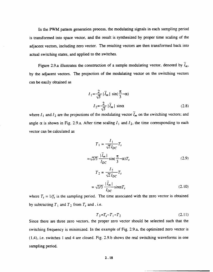
In the PWM pattern generation process, the moduiating signals in each sarnpling penod
is transformed into space vector, and the result is synthesized by proper time scaiing of the
adjacent vectors, including zero vector. The resulting vectors are then ~ansformed back inro
actual switching States, and applied to the switches.
Figure 2.9.a illustrates the construction of a sample modulating vector. denoted by Ï,,
by the adjacent vectors. The projection of the modulating vector on the switching vectors
can be easily obtained as
2 - 12=- 1 Im 1 sina fi
(2.8)
where I l and I 2 are the projections of the moduiating vector Ïm on the switching vectors; and
angle a is shown in Fig. 2.9.a. After time scaling I I and I I , the tirne corresponding to each
vector can be calculated as
~ D C
where Ts = l/fs is the sarnpling period. The time associated with the zero vector is obtained
by subtracting T l and T 2 from T, and . i.e.
Since there are three zero vecton. the proper zero vector should be selected such that the
switching frequency is minimized. In the example of Fig. 2.9.a. the optimized zero vector is
(1,4), i.e. switches 1 and 4 are closed. Fig. 2.9.b shows the real switching waveforms in one
sarnpling period.

Figure 2.9. (a) Synthesizing a space vector by adjacent vecton and (b) the actuai switching waveforms.
To calculate the maximum modulation index in this rnethod, one may note that the sum
of T I and T 2 should be less than or equai to the sampling penod Tx, Le.
TI+T2<T, Substituting Eqn. 2.9 and 2.10 in 2.12 yields
The maximum achievable amplitude of the modulating vector now can be obtained as
which based on Eqn. 2.6 is corresponding to the maximum fundamental amplitude of
i
This results in the maximum modulation index equal to

rn ,, a.707 (2.15)
Based on Fig. 2.9.b, one switching action takes place for the switches 2.4 and 6 in each
sampling period. Since each switch is active just during hdf of the fundamental period. it can
be realized that the average switching frequency f, in the SV-PWM method is half of the
carrier (sampling) frequency, i.e.
Unlike the SHE-PWM method, no analytical expression exists for the amplitude of har-
monics in the SV-PWM methods, and so they have to be obtained by empirical methods.
It is clear that SV-PWM rnethod has on-line computational tasks. Although these com-
putations can be implemented entirely by hardware and by using look up tables. this rnethod
is mostly suited for the applications in which rnicrocontroilers or Digital signal Processors
(DSP) are employed in the control circuit.
2.2.5. Sinusoidal PWM (SIN-PWM) Method
In carrier based SIN-PWM methods. the PWM patterns are generated by cornparing the
modulating waveform with a carrier signal. as shown in Fig. 2.10 for two types of carrier sig-
nais. namely triangular and sawtwth. In these methods, the modulation index is sometimes
defined as the ratio of peak modulating signal to the peak camer signal. i.e.
where cm and G, are the peak modulating and carrier waveforms respectively. Note that
based on this definition. M > 1 corresponds to overmodulation.
It was pointed out in Sec. 2.3.1 that the PWM patterns of three legs in a three-phase
bridge CTC (Fig. 2.5) must be generated with respect to each other. As a result. unlike
VTC-PWM. the SIN-PWM generation technique cannot be independently applied to each

Figure 2.10. Generation of PWM signals in SIN-PWM method with (a) tnangular carrier signal and (b) sawtooth carrier signal.
leg in a three-phase CTC. However. by considenng the duality concepts between VTC and
CTC, and inspecting the AC line currents depicted in Fig. 2.6, a sirnilarity could be recog-
nized between line voltages in a VTC and line currents in a CTC as will be explained in the
following [28].
The possible combinations of 2-level PWM patterns (corresponding to pole voltages in
a VTC) and the resulting 3-level PWM patterns (corresponding to line voltages in a VTC)
are shown in Table 3.2. Close inspection of 3-level PWM patterns shows that they comply
with the basic niles mentioned in Sec. 2.3, i.e at each instant the logical level of only one line
voltage is either 1 or - 1. and in some instants al1 three line voltages are zero. An immediate

but important result of this similarity is that the PWM pattems for line currents in CTC cm
be generated in the sarne way as the PWM pattems for line voltages are generated in VTC:
Le., by subsequent subtraction of three 120' phase shifted 2-level PWM pattems. as illus-
trated in Fig. 2.1 I. Using the proposed method, the basic PWM patterns for the line currents
in a CTC can be generated. It should be noted, however, that these pattems are not the gating
pattems which are to be applied to the switches. To convert the line PWM patterns to six
gating patterns corresponding to converter switches, an additional circuitry is to be used.
Using niangular waveform as the carrier signal in the SIN-PWM method resuits in
hdf-wave symmetry and thus no even harmonics appear in the PWM waveforms. It can be
shown that the average switching frequency in this case is equal to the carrier frequency, i.e.
fw,m = f c (2.18)
On the other hand, when sawtooth waveform is employed as the carrier frequency. the
half wave symmetry is not preserved anyrnore. resulting in even harmonics in the PWM
waveforms. (However, as long as the frequency of these harmonics is high. they are
attenuated by the inputloutput low pas filters and thus their adverse effect can be neglected.
An interesting prOpeRy of the SIN-PWM technique with sawtooth carrier is that the
average switching frequency is half of the carrier frequency, i.e.
This reduction in the switching frequency cm be explained by inspecting Fig. 2.12. It cari be
seen that the intermediate 2-level signals in this figure have one coinciding transition, which
is not reflected on the line PWM patterns, and consequently on the gating patterns.
Like other carrier based PWM methods, the harmonic spectra of the PWM waveforms
in the SIN-PWM method consist of fundamental frequency plus side band harmonics around
the camer frequency and its integer multiples. The amplitudes of these harmonics are
independent of rnf and cm be analytically expressed in tems of modulation index M, as will


Figure 2.12. Illustration of the reduction of switching frequency in SIN-PWM method when the c h e r is a sawtooth signal. (a) Carrier and modulating waveforms. (b) and (c) two-level PWM patterns and (d) resultant three-level PWM patterns corresponding to line current pat- terns.
be explained in Chapter 3.
To calculate the maximum achievable fundamental AC current corresponding to m,
in SIN-PWM method. consider Fig. 2.9 in which the peak fundamental AC component in the
2-level PWM waveforms is given by
A M ~ . ~ e v e ! = - (2.20) 2
where M is given by Eqn. 2.17. Note that the 2-level signals have a DC component equal to
0.5. Therefore. the resultant 3-level signals. derived by subsequent subtraction of 120' phase
shifted 2-level signals. have the peak fundamental value of

L
The actual PWM waveforms, i.e. the AC line currents, have the amplitude of idDc
fore. the rrns value of the fundamental line currents in terms of rn and IDc is given by
The maximum fundamental line current corresponding to M = I is then obtained as
Consequently the maximum modulation index rn, is given by
The relationship between m and M is dso obtained as
(2.21)
There-
7 37) (-.-a
(2.23)
(2.24)
(2.25)
To increase the maximum modulation index in the SIN-PWM method, it has been pro-
posed to add the third harmonic to the modulating waveforms [29]. This method. called
SIN#-PWM hereafter. produces flat top modutating signals with higher fundamental value.
while the additional third harmonic does not appear in the output three-phase waveforms. It
is shown that by adding the third harmonic with the amplitude of 1 / 6 of the fundamentai.
the amplitude of the fundamenral PWM waveform can be increased as much as
2 / fi =15.5%. Thus. the maximum modulation index with this method is given by
which is identical to SHE-PWM and SV-PWM methods.
2.2.6. Cornparison and Selection
In this section. the performance of CTC-PWM techniques expiained earlier is discussed
and compared. h this way, the following performance criteria are considered:

Potential dynamic performance of the system in which the PWM technique is
employed.
The average switching frequency f,.
The maximum modulation index rn ,, . Overmodulation capability, Le., the performance of the method when the moduiauon
index m is set to be higher than m ,, . Low frequency characteristic of the method during open loop and closed loop opera-
tion.
Table 2.3 surnrnarizes the performance of the described CTC-PWM techniques.
Generally speaking, the implementaûon of SHE-PWM methods results in slow dynamic
response. Different methods have been proposed to overcome this slupgish performance,
however they usually sacrifice the main feature of the method, i-e. defined harmonic spec-
trum. Since fast dynarnic response is one of the key performance specifications in the pro-
posed system, the SHE-PWM method is not considered as a potential PWM method in this
thesis.
As stated in Sec. 2-32, operation in overmodulation region results in large low fre-
quency hmonics. Since the filter design is generaiiy carried out based on high frequency
hmonics. the overmodulation operation then cannot be tolerated. On the other hand. over-
moduiation is possible to some extent in closed loop operation of SIN-PWM methods. as will
be explained in Chapter 4.
Based on Table 2.3, it can be seen that mm, is the highest for SV-PWM and SIN3-
PWM methods. On the other hand. the switching frequency is the lowest for SV-PWM and
sawtooth based SIN-PWM rnethods. Therefore, both SV-PWM and SIN3-PWM methods
demonstrate the same performance from the switching frequency and maximum modulation
index point of view. While SIN3-PWM method can be ernployed in the proposed rectifier


control system, its implementation is not feasible in the inverter control system. Therefore.
only SV-PWM method is suited for implementation in the inverter control system. However.
this method shows relatively large low frequency harmonics, which are hard to filter out.
Sarne characteristic appears in closed loop operation of sawtooth carrier based SIN-PWM
methods. This phenomenon in both techniques can be contributed to the unsymmetrical
nature of PWM waveforms.
Triangular carrier based SIN-PWM shows lower rn, and higher switching frequency
than other methods. However, it has the best closed loop performance arnong other methods
from the low frequency harmonics point of view . Moreover, its overmodulation capability
without substantial increase of low frequency harmonics is advantageous in overload condi-
tions. As a result, this method is the best choice for low distortion CTC based power supply
applications.
2.3. Basic System Operation
In this section. the basic operation of the system is explained by the help of illustrative
waveforms obtained from the theoretical venfications. These waveforms are. obtained using, a
cornputer program for time-domain simulation of different stages of the proposed system.
The system operates with constant DC current under al1 operating conditions. To main-
tain constant DC current, the average DC voltage across the DC inductor (LDc in Fig. 7-11
must be kept constant. The voltage across the DC inductor is the difference between the
rectifier output voltage voc,, and the inverter input voltage v ~ c i . The average inverter input
voltage VDc,i is a load dependent quantity and hence not controllable. Therefore to control
the average DC voltage across the DC inductor, the rectifier average output voltage Voc,,
has to be controlled. Thus. any change in the average inverter input voltage VDc,i due to sys-
tem load change is compensated by the average rectifier output voltage VDc, such that the
fixed DC current is maintained in the intermediate link.

It will be shown in Chapter 3 that with unity power factor operation. the average
rectifier output voltage is given by
V D c = k M (3.37)
where k is constant dependent on both the amplinide of AC voltage and PWM method: and
M is the modulation index. As a result, the average rectifier output voltage VDc,, can be
linearly controlled by the rectifier modulation index M,. Now considering Fig. 2.1. the
rectifier modulating signal m, is the product of current template signals iRmp and the rectifier
controller output u,. This means that the rectifier modulation index M, is proportional to the
rectifier controller output u,, and therefore based on Eqn. 2.27 the average rectifier output
voltage VDc, cm be linearly controlled by this signal. Under closed loop operation. the
rectifier controller detects the error signal between the Iink current iK and the reference
current I * , and adjusts its output u, (corresponding to M,) such that the average DC current
remains constant.
Figure 2.13 indicates the rectifier response to a step load change. As explained above.
the output load change is reflected on the rectifier by rneans of a change in the average vol-
tage in the intermediate Iink. A decrease in the output load follows by a decrease in the aver-
age inverter input voltage VDcSi (Fig. 2.13.b). This change tends to increase the current in the
DC link. which is consequently detected by the rectifier control system. and causes the aver-
age rectifier output voltage to be decreased (Fig. 2 . 1 3 . ~ ) . The amplitude of input current i, is
also decreased as a result of power balance. whereas the unity power factor is aiways main-
tained (Fig. 2.13.g). Noce that how the average rectifier output voltage follows the controller
output signal, which in tum is proportional to the rectifier modulation index M,.
The output voltage v, is controlled by controlling the fundamental inverter output
current ii. 1 . Since the DC current is fixed in the system. then based on Eqn. 2.2 the funda-
mental AC current should be controlled by rneans of modulation index. Concerning Fig. 2.1.
the inverter modulating signals rn, directly corne from the inverter controller output ui.

Figure 2.13. Rectifier response to the step load change. (a) Load current i,, (b) average in- verter input voltage VDci , (c) average rectifier output voltage VDc,,, (d) rectifier controller output u,, (e) Dc current iDc. (f) input voltage v, and (g) input current i,.

Under closed loop operation, the amplitude of these signais and hence the inverter modula-
tion index Mi is adjusted such that the desired output voltage is maintained.
Fig. 2.14 shows the inverter response to a step load change. As can be seen. when the
load is decreased. the amplitude of modulating signal mi is decreased as well. and therefore
the fundamentai inverter output current ii, 1 is reduced as a consequence. This. in turn. results
in fixed output voltage.
2.4. Operation Under Unbalanced and Noniinear Loads
This thesis is focused on the system operation under balanced and Iinear loads. There-
fore. the system analysis and design is carried out based on this assumption. Despite that, the
system performance under unbalanced and noniinear loads is also demonstrated in this sec-
tion. The following results are obtained from time domain simulation of the system
descnbed in Design Example 1 presented in Chapter 5.
Figure 2.15 indicates the system response to an unbalanced condition when one phase is
open. The measured rms value of line voltages is equd to the rated value for al1 three
phases. showing that there is no imbdance at the output voltages. The measured THDVt, for
dl phase voltages is also less than the given value.
Figure 2.16 dernonstrates the system response to a nonlinear load when it is exposed to
a three-phase diode rectifier. Nonlinear loads usudly inject low order and non-characteristic
h m o n i c currents into the output terminais. Since the output filter is generally designed with
respect to high frequency harmonics around the switching frequency, these harmonics are
not filtered out and result in distoned output voltage. On the other hand. closed loop opera-
tion of the system dong with its fast transient response causes the modulating signals mi to
change in such a way that the low order and non-charactenstic harmonics are compensated,
as shown in Fig. 1.16.~. Therefore, the voltage distortion under closed loop operation is

(dl
Figure 2.14. Invener response to the step load change. (a) Load voltage v,. (b) load current, ( c ) inverter modulating signal mi. (d) inverter output current ii and (e) fundamental inverter Output CUITent ii, 1 .

much less than that in open loop. The measured THDVo in this case is 1.7%. Le. 70% more
than the calculated value for linear loads.
(b) Time (2 rnsecJdiv.)
Figure 2.15. Steady state system response to unbalanced load when one phase is open. (a) Output voltages and (b) output currents.
Time (2 msecJdiv.)
Figure 2.16. Steady state system response to a nonlinear load consisting of a diode rectifier. (a) Output voltage v,. (b) output current i, and (c) inverter modulating signal mi.

CHAPTER 3
STEADY STATE ANALYSIS OF
A CURRENT LINK AC TO AC POWER SUPPLY
Introduction
The basic operation and the structure of the proposed AC to AC power supply dong
with the charactenstics of PWM techniques in current type converters were studied in
Chapter 2. This chapter presents a comprehensive steady-state analysis to provide the basic
understanding of the steady-state characteristics and performance of the system.
Specificalty, the essential relationships between fundamentaVharmonic components of
ACDC voltages and currents are derived and input/intermediate/output filters are analyzed.
Therefore. this chapter is the b a i s for the steady-state system design presented in Chapter 5.
The anaiysis in this chapter is based on the simplifying assumptions mentioned in Sec 3.1.
The steady-state analysis in this chapter relies on the representation of PWM
wavefoms by their corresponding Fourier Series. It was explained in Chapter 2 that SIN-
PWM technique is adapted for both rectifier and inverter in the proposed system. In such
techniques, the Fourier coefficients of the PWM wavefoms, which also represent the ampli-
tude of the corresponding harmonics, can be calculated by andytical or empirical approaches
[30]. As will be seen. the amplitude of harmonics in the employed PWM technique is
independent of the switching frequency. and thus a generalized h m o n i c anaiysis can be

performed without any knowledge about the switching frequency.
The first step in the steady-state analysis is steady-state system modeling. Like any
other power elecuonics circuit, the system model consists of linear circuit elements plus
non-sinusoidal (PWM) sources. Using Fourier anaiysis. these non-sinusoidal sources are
replaced by a series of sinusoidai sources. As a result, a set of linear models at the funda-
mental and harmonic frequencies is obtained. The fundamental model is used to srudy the
relationships between hindamental quantities and the basic power transfer scheme in the sys-
tem. The harmonic models, on the other hand, are employed to denve the relevant relation-
ships between the harmonic distortion. filter components and PWM parameters.
The content of this chapter is organized as follows.
In Section 1. the basic simplifying assumptions for the steady-state analysis are men-
tioned.
In Section 2. the steady-state analysis of the rectifier is camied out. The rectifier model
as seen from the AC side is obtained. Requiremenü for unity power factor operation are
derived in terms of system parameters. A closed form expression is denved for distortion of
the input current in rems of input filter and system parameters. Ratings of the components
are calculated.
Section 3 presents the steady-state analysis of the inverter. The inverter mode1 from the
AC side is denved. Impact of output filter on the system rating is studied. The output voltage
distortion is calculated in a closed form in terms of output filter and system parameten. The
components' ratings are calculated. Two configurations considered in this analysis are: ( 1 )
System without isolating transfomer at the output terrninals and (2) system with isolating
transformer. Characteristics of each configuration are mentioned.
In Section 4, the
The fundamentai and
steady-state characteristics of the intermediate DC link are studied.
hmonic models are derived. General relationships between the

fundamental and harmonies of the DUAC quantities in a current type converter are derived.
The ripple current in the DC link is calculated in terms of DC filter and other systern parame-
ters.
Section 5 presents the theoreticai and experimental verifications of the predicted results.
The time domain simulation of the system provides the theoretical results, and the expen-
mental setup explained in Chapter 2 is employed to obtain the experimental wavefonns.
In Section 6, the overall system performance as an AC to AC converter is exarnined.
The system operation as an AC voltage booster is described. The advantages and disadvan-
tages of such an operating condition are mentioned.
3.1. Simpiifying Assumptions
The steady-state anaiysis in this chapter is carried out based on the following simplify-
ing assumptions, unless otherwise stated:
- The intermediate DC link current is ripple free.
- The commutation times and on-state voltage drops in the switching devices are
neglected. Further. the effect of snubber circuits employed in a real system is not con-
sidered.
- A11 modulating signals are sinusoidal waveforms.
- The modulation is performed only in the linear region, i.e. overmodulation is not con-
sidered (O I M 4 1 ).
- Only balanced operation is considered.
- Al1 circuit elements such as capacitors, inductors and sources are ideal.

- Only dominant harmonics of the PWM wavefonns are taken into consideration.
subscripts r and i in this thesis chapter are used to avoid clutter between rectifier and
inverter related quantities. In some designated sections, however. this notation is omitted for
simplicity.
The bold capital letters like V and I generally denote phasor quantiues. and the normal
capital letters like V and I denote their corresponding amplitudes. Further. subscript 1 and n
denote the fundamental and harmonic components respectively. Subscript 1 is not used for
reactances at hindamental frequency.
Most of the calculations in this chapter are performed in permit- basis with load side
quantities as the base vaiues.
3.2. Rectifier Steady-State Analysis
The rectifier operation was described in Chapter 2. The main objective of this section is
to derive the basic steady-state expressions which govern the rectifier operation. To avoid
unnecessary lengthy subscripts. subscript r i s not used for filter components in this section.
The rectifier model for the fundamental and h m o n i c frequencies is obtained. Balanced
operation ailows using single phase equivalent model for the purpose of analysis. Relevant
graphs and expressions for unity power factor operation and input filter design are provided.
The components ratings are calcuïated. Theoretical and experimental verifications are given.
3.2.1. Steady-State Modeling
The power circuit structure of the front end current type rectifier is shown in Fig. 3.1.
The rectifier input current i K j =a. b. c ) is a PWM current which contains harmonics
around the carrier frequency and its integer multiples. Therefore. if seen €rom the AC side,
the rectifier can be modeled by a harmonic current source and its associated filter corn-

ponents, as indicated in Fig. 3.2.a for a single phase equivalent circuit. In this model. i,
represents the instantaneous value of the rectifier input current. For the purpose of steady-
state analysis, the model of Fig. 3.2.a is further broken up into two equivalent circuits respec-
tively reprcsenting the fundarnental and harmonic currenü. as shown in Fig. 3.2.b.c. Note
that in these models. the instantaneous values are replaced by the phasor quantities. in which
subscript 1 denotes the fundamental values and subscnpt n denotes the nth harmonic corn-
ponent.
3.2.2. Unity Power Factor Operation
One of the major functions of the front end rectifier is to maintain unity power factor
input current. This is basically achieved by controlling the phase angle between the rectifier
input current i, and the source voltage v, (Fig. 3.1). which is investigated in this section.
Considenng the equivalent circuit of Fig. 3.2.b. and taking the supply voltage Vs as the
reference. the fundamental supply current I , 1 can be obtained by using superposition as
where X,= l/ o,C and X,= o r L are the filter capacitor and filter inductor reactances respec-
tively. o, is the fundamental frequency. and I , 1 and Ir, 1 are the corresponding fûndamental
phasors quantities. Note that subscnpt 1 is not used for V,, because the input supply is
assumed to be an ideal sinusoidal source at the fundarnental frequency. Fig. 3.3 shows the
phasor diagrarn representing the fundamental quantities. in which $s and y, are the phase
angles of the supply current k 1 and rectifier input current Ir, respectively. Based on Eqn.
3.1 and Fig. 3.3. Q, can be obtained as

Figure 3.1. Power circuit structure of a current current type rectifier (CTR).
Figure 3.2. Single phase equivalent circuits of a current type rectifier (CTR) representing (a) instantaneous quantities. (b) fundamental phasor quantities and (c) harmonic phasor quanti- ties.
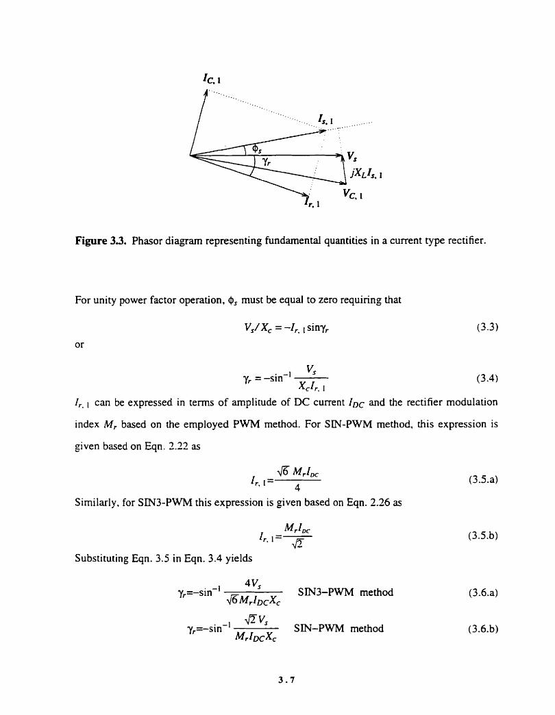
Figure 3.3. Phasor diagrarn representing fundamentai quantities in a current type rectifier.
For unity power factor operation, Q, must be equal to zero requiring that
, c m be expressed in tems of amplitude of DC current IDc and the rectifier modulation
index Mr based on the employed PWM method. For SN-PWM method, this expression is
given based on Eqn. 2.22 as
Similarly, for SIN3-PWM this expression is given based on Eqn. 2.26 as
Substituting Eqn. 3.5 in Eqn. 3.4 yields
y,=-sin-' 4 v s
SIN3-PWM rnethod J ~ M ~ I D c X C
yr=-sin-' v s
SN-PWM method M r r ~ ~ &

Neglecting input voltage variations, ail the parameten but M, in Eqn. 3:6 are constant. there-
fore it can be written as
in which
- - 3
Ks= 6 ID& SIN-PWM method
4% K,=- SIN3-PWM method (3.8.b) ID&
Eqn. 3.7 expresses the requirement for having unity power factor input current. Fig. 3.4
shows the phasor diagram corresponding to this operating condition. It is ncteworthy that
Eqn. 3.7 is independent of the filter inauctance, i.e. the source interna1 impedance.
Eqn 3.7 may not be satisfied for M, < Ks. In this case if y, is set to -90 O . the amplitude
of the fundamental supply current is computed based on Eqn. 3.1. as
Figure 3.4. Phasor diagram representing fundamental quantities corresponding to unity power factor operation (i.e. @, = O) in a current type rectifier.

Note that in this case 1,1 is pure capacitive.
As another special case, if yr is set to zero for al1 operating conditions. then based on
Eqn. 3.2 Qs is given by
= tan- 1 v s w
1, In this case and for high switching frequency applications in which C is relatively srnaIl. @,
becomes smail for operating conditions close to the rated load. For light loads. Ir becomes
small and qS starts becoming large as a consequence. i.e. the supply current tends to become
more capacitive. n ie phasor diagrarns corresponding to this operating condition is illustrated
in Fig. 3.5.
3.2.3. Input Filter Analysis
The rectifier input filter is studied in this section based on the Fourier anaiysis of the
PWM waveforms. The objective of this section is to obtain relevant graphs andor expres-
sions for the input filter design. This analysis is systematically performed for the SIN3-
Figure 3.5. Phasor diagrarn representing fundamental quantities corresponding to the rectifier operation when Ir, 1 is in phase with V'.

PWM method with sawtooth carrier based on the information provided in Chapter 2. how-
ever, the method can be applied to any other PWM scheme.
As stated in Sec. 2.2. the amplitude of harmonics in SIN3-PWM method is independent
of the switching frequency and can be given as a function of modulation index M, and the
amplitude of DC current IDc. Using andytical or empirical approaches [30], the normalized
amplitude of dominant harmnics in the rectifier input current ir cm be obtained as tabulated
in Table 3.1. The quantities in this table are normalized with respect to the maximum funda-
mental value corresponding to M,=l. Note that the entries in this table are not a function of
ml. but mf defines the frequencies at which they occur.
The primary function of the input filter is to attenuate the harmonics of the rectifier
input current ir and provide low distortion supply current i, (Fig. 3.1). As explained in Sec.
2.3, the current distortion c m be quantified by a quantity called the total harmonic distortion
THD. Thus. expressing Eqn. 2.1 for the supply current i, yields
where n is the harmonic number, THDIT is the total harmonic distonion in the supply current.
and I,., is the normalized amplitude of the nth h m o n i c in the supply current i,. The
rectifier input filter is designed such that THDI, does not exceed a given level under al1
operating conditions. In this analysis, therefore, the worst case should be taken into con-
sideration to ensure satisfactory results for al1 other operating conditions.
Using the harmonic equivalent
h m o n i c components of the rectifier
mode1 of Fig. 3.2.c. Ir,, cm be expressed in terms of
input current ir and the input filter parameters as
where X,, and XLn are the corresponding reactances at the nth h m o n i c frequency. and Ir,,
is the normalized amplitude of the nth harmonic in the rectifier input current. Considering

Table 3.1. Normalized amplitude of harmonics with respect to the maximum fundamental value (2 i,m) for SIN3-PWM method with sawtooth carrier.
Modulation index M
Figure 3.6. Total current harrnonic distonion of the rectifier input current (THDL) versus M, for sawtooth based SIN3-PWM.

that
yields
where n is the harmonic number. To find the worst case from the current distortion point of
view, consider Fig. 3.6 which illustrates the variation of total current harmonic distortion in
the rectifier input current, denoted by THDIr. versus M,. This graph shows that the maximum
THDb occurs around M,= 0.6, which can be considered as the worst case. Therefore. using
the numerical values from Table 3.1 corresponding to M 4 . 6 , the maximum THDl, can be
calculated. On the other hand, by proper simpliQing assumptions, a closed expression can be
obtained for the maximum THDIr as will be explained in the following.
Based on Table 3.1. the harmonics around mf have the major contribution in high
current distonion around M,=û.6. Therefore. considering the fact that the harmonics around
Zmfi 3 9 - and - - - have iower amplitudes. and that they are anenuated by the power of two
by the second order input filter, their impact on THDI, cm be neglected without noticeable
error. Doing this. and substituting Eqn. 3.14 for dominant harmonics into Eqn. 3.1 1 results in
~ h e r e Imrl , I,,.+l - . . are the normalized amplitude of dominant h m o n i c s around ml.
Also. for large mf it can be assumed that
r n ~ = rnfk 1 = mfk2 = m f 3 = mlk4 = m f ~
which further simplifies Eqn. 3.15 to

Note that Imp1=ITI, Ims=l+ and so on. The above sum is maximized around M = 0.6
as mentioned earlier, and thus can be calculated using entries of Table 3.1. To do this. how-
ever, the normalized entries of ~ i ib le 3.1 must be transformed into the system perunit bais.
Based on Eqn 2.26. the maximum rms value of the fundamental rectifier input current is a
function of amplitude of the DC current and is given by
where IDc is the amplitude of DC current. Therefore, to express the entries of Table 3.1 in
the system perunit basis, they should be multiplied by
Kpu = I D C / ~
(3.19) IB
where IB is the base current in the system perunit basis. Note that K,, is typically very close
to 1. Now substituting the numerical values corresponding to M, = 0.6 from Table 3.1 into
Eqn. (3.17) yieids
0.376 X, ID, THDI, = (3.20)
Is ( m; X,-Xc )
which is a closed formula for THD!, in terms of system parameters. Eqn. 3.20 can be also
expressed in terms of input filter capacitance and inductance as
where or is the fundamental supply frequency and L and C are the filter inductance and
capacitance respectively. For different PWM schemes, the same expression with different
coefficient can be obtained.
THDI, Figure 3.7 shows the variation of - versus mf for different values of w f LC for
Kr
two cases; one by using Eqn. 3.1 1 and taking al1 hmonic currents listed in Table 3.1 into

Figure 3.7. Variation of THD,,/K,, versus mf for different values of of^^ for two cases; one based on Eqn. 3.1 1 and using Table 3.1. and the other based on Eqn. 3.2 1.
consideration. and the other by using Eqn. 3.21. The mal1 difference shows the validity of
the above approximation within the illustrated range.
3.2.4. Component Rating
Generally speaking. the current rating of the components in the system is a function of
amplitude of DC current. which in tum is dependent on the system power rating and inverter
output fitter structure. The voltage rating. on the other hand, is dependent on the AC side
voltage amplitude. In this section. the curreni rating of different components in the rectifier
section is calculated. The cornponents should be able to withstand the worst operating con-
ditions, therefore the worst case is considered in the following calculations.

(i) Filter inductor
The filter inductor current is the same as the supply current and its m s value is given by
where I,,, is the nth harmonic component in the supply current. Assuming normalized quan-
tities, the second term in Eqn. 3.22 is equd to the squared total current harmonic distonion in
the supply current. thus
1/2 I~, , .=[I: + T H D ~ ] pemnit
Since the maximum THDI, is normally much srnaller than the maximum I,, 1 (in the pemnit
basis), then Eqn. 3.23 with a good approximation is equal to * - -
IL.-=~. 1 (3 -24) That is. the rms value of the filter inductor current is equal to the rated input current.
(ii) Filter capacitor
With the similar procedure. the rms value of the filter capacitor current km in the
permit bais is obtained as
where THDI, is the total current harmonic distortion of the capacitor current &. The reac-
tance of the filter capacitance in harmonic frequencies is much smaller than the reactance of
the filter inductance. Therefore. i t can be assumed that al1 current harmonics in the rectifier
input current i, flow inro the capacitor. and thus
THD,,=THD,, pemnit (3.26)
On the other hand based on Fig. 3.4. the fundamental capacitor current is given by

Since X, is usually srndl, Eqn. 3.27 can be written as
Substituting into Eqn. 3.25 yields
in which the maximum THDl should be considered as the worst case. Based on Fig. 3.6. the
maximum THDIr is
perunit basis. Doing
0.64 which should be rnultiplied by Kp to be expressed in the system
so, Eqn. 3.28 can be written as
Ic,,=7+0.64 Kpu perunit [4 21'n where %, is given by Eqn. 3.19.
(iii) Semiconductor switches
To calculate the current rating of the semiconductor switches, the DC current is written
in tems of switch currents as
ioc=is, +iS, +irs (3.30)
where iDc, is, , is, and is, are the instantaneous values of currents. Squaring and integrating
Eqn. 3.30 over one period yields
The left hand side and the first three tenns in the right hand side of Eqn. 3.3 1 denote the
squared rms value of the cuments. On the other hand. the last three terms in the right hand
side of Eqn. 3.3 1 are zero, because two upper switches in a three-phase bridge CTC cannot
conduct simultaneously. Further, since the npple current in the DC link is small, its rms
value is very close to its DC value. Therefore

2 &=d, .-4,. -+h,. M (3.32)
Finally, because of the symmetry, the rms value of the currents in al1 switches is equal, and
thus it cm be written as
Similarly by averaging Eqn. 3.30 over one period, the DC value of the switch currents
is obtained as
3.3. Inverter Steady-State Analysis
The intermediate DC current is converted to PWM AC currents by means of a current
type inverter (0. These AC PWM currents charge/discharge output capacitors and result
output AC voltages. The main objective of this section is to study the steady-state charac-
tenstics of this conversion. Subscript i is not used for the filter components in this section.
The inverter modeling is performed when seen from the AC terminals. Balanced opera-
tion allows use of single phase models for analysis. The fundamental model is used to inves-
tigate the relationships hetween the fundamental quantities. and the harmonic model is used
for output filter anaiysis. The application of isolating transformer and its impact on the fun-
damental quantities is considered in detail. The cornponents rating is calculated.
3.3.1. S teady-S tate Modeling
Figure 3.8 shows the inverter power circuit structure. As in the rectifier case. the PWM
AC currents ii,, CI-. b. c) contain harmonies around the integer multiples of the frequency
modulation ratio mf. Therefore. the inverter can be modeled by a harmonic current source
and its associated output filter capacitor, as shown in Fig. 3.9.a for the single phase
equivalent circuit. Note that in this model ii represents the instantaneous value of the inverter

Figure 3.8. Power circuit structure of a current type inverter (CTI).
Figure 3.9. Single phase equivalent circuits of a current type inverter ((JI?) representing (a) instantaneous quantities. (b) fundamental phasor quantities and (c) h m o n i c phasor quanti- ties.
output current. This mode1 can be broken up into two equivalent circuits representing the
hindamental and harmonic quantities, as shown in Fig. 3.9.b.c. Again the quantities in Fig.
3.9.b.c are phasor quantities with subscnpt I and n denoting the fundarnental and harmonic
components respectively.
An isolating transformer is sometimes employed at the system output for voltage
matching andlor isolation. The rnagnetizing inductance of this transformer is sometimes
tuned with the filter capacitance at the fundarnental frequency ai. Doing sa. the output capa-
citor does not draw fundarnental current from the system, resulting in lower system current
rating. The leakage inductance of this transformer is normally small, and its influence on the
steady-state operation can be neglected. Therefore the transformer can be modeled by a
shunt reactance representing the magnetizing inductance. as shown in Fig. 3-10. Note that in
Figure 3.10. Single phase equivalent circuits of a current type inverter (CTI) with isolating transformer representing (a) instantaneous quantities, (b) fundamental phasor quantities and (c) harmonic phasor quantities.

this mode1 the core losses are not also taken into account for their negligible effect on the
steady-state operation. Based on the above assumption, the magnetizing inductance of the
isolating transformer c m be obtained as
1 LM=- ofc
where is the fundamental output frequency.
3.3.2. Relationship Between Fundamental Quantities
The fundamental inverter (system) output voltage V,, 1 is a function of fundamental
inverter output current Ii, 1 and the output filter configuration. Assuming no isolating
transformer at the system output and taking the Fundamental output voltage V,, 1 as the refer-
ence. then based on the equivalent circuit of Fig. 3.9.b the fundarnental invener output
current is given by
where Xc=l/oiC is the perunit reactance of the filter capacitor. The phasor diagram
representing fundamental components is shown in Fig. 3.1 La. Based on Eqn. 3.36. the fun-
darnental inverter output current 1,. ] is a function of output capacitor reactance. The varia-
tion of I,, 1 versus Xc is shown in Fig. 3.12 for the rated load with different power factors. It
can be seen that the fundamental invener output current Ii. can be as much as twice the
rated output current in this case.
In the case of using isolating transformer with tuned magnetizing inductance, the funda-
mental capacitor current Ic* 1 is compensated by the fundamental magnetizing current IM. 1.
and ihus the invener does not supply fondamental current to the output filter. As a conse-
quence. the fundamental invener output current li, 1 is always equal to the fundarnental load
current Io, 1 . i.e.
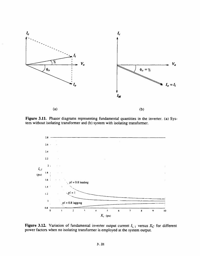
Figure 3.11. Phasor diagrams representing fiindamental quantities in the inverter. (a) Sys- tem without isolating transformer and (b) system with isolating transformer.
1 . 6 ; . . ., pf = 0.8 leading
Figure 3.12. Variation of fundamental inverter output current Ii, versus Xc for different power factors when no isolating transformer is employed at the system output.

The phasor diagrarn corresponding to this operating condition is shown in Fig. 3.1 I .b. As
can be seen, one of the advantages of using isolating transformer is that the impact of output
filter on the fundamental currents can be eliminated, resulting in lower system current rating.
33.3. Output Filter Analysis
Sirnilar to the analysis of Sec. 3.1. the inverter output current ii can be represented by
its fundamental value plus a set of harmonic current sources. The amplitude of these harmon-
ics is a function of employed P W scherne. It was shown in Chapter 2 that SIN-PWM
method has the best performance in elimination of low frequency harmonics. Furthemore.
usïng triangular carrier waveform ensures symmetry and minimum distortion at the output
voltage. Therefore, the harmonic analysis in this section is performed based on SIN-PWM
scheme with triangular carrier. Needless to Say, this analysis can be extended to any other
PWM scheme.
The amplitude of harmonics in SIN-PWM scheme with triangular carrier can be analyt-
ically expressed as a function of modulation index Mi and the amplitude of DC current [30]
as
21Dc M i j x I,=-Jk( 7 ) k is odd)
J X - where j.k = 0.1.2, - . . , h=jm$k. II, is a Bessel function of the first kind of the order of k
Mi jx: and argument - , In is the amplitude of the nth hamonic current. and IDc is the ampli-
2
tude of the DC current. Note that Eqn. 3.38 holds for large ml, namely mf>9.
Theoretically, rnf can take on any integer value for the synchronized PWM scheme.
However. an odd integer is commonly chosen such that even harmonics at the output
waveforms are eliminated. Besides, by choosing ml a multiple of 3 in 3 phase systems, the
dominant harmonic at m~ can be also elirninated using only one carrier signal for ail three-

phases. In this thesis, it is assumed that rnf is an odd multiple of 3 hereafter. Table 3.2 shows
the normdized amplitude of the fint dominant harmonics in the line current with respect to
the maximum fundamental value corresponding to Mi= 1. Consequently. the total current har-
monic distortion in the iine currents ii, denoted by THDI,, is given by Eqn. 2.1 and depicted
in Fig. 3.13 versus modulation index Mi.
The function of the output filter is to absorb the high frequency harmonics of the
rectifier output current ii and provide low distortion output voltage. The voltage distortion in
the output voltage is expressed by the total voltage harmonic distortion THDv and defined
where V,,, is the normalized amplitude of the nth harmonic voltage. The output filter is
designed such that 77YDVn requirement is maintained for al1 operating conditions. Therefore.
the foilowing analysis is performed for the worsr case.
Considering the equivalent hamonic mode1 shown in Fig. 3.9.c and 3.10.c. the reac-
tance of the output capacitor seen by the high frequency current harmonics is smaller rhan
the load impedance and magnetizing reactance. Therefore. almost ail current harmonics flow
through the capacitor. and the output voltage distonion becomes rnainly due to the voltage
drops across the output capacitor caused by the current harmonics. As a result, the equivalent
circuit of Fig. 3.9.c is adequate for the purpose of THDy calculation. Based on this
simplification. Eqn. 3.39 can be wrinen in terms of harmonic content components of the
inverter output current and the output filter panmeten as

Table 3.2. Normaiized amplitude of harmonies wirh respect to the maximum fundamental value ( I for SIN-PWM method with triangular carrier.
Modulation index M
Figure 3.13. Total current h m o n i c distortion of the invener output current (THDG ) versus Mi for triangular based SIN-PWM.

where Xc.,=Xc/n is the perunit capacitor reactance of the output filter at the nth hannonic
frequency, Xc is the perunit reactance of the filter capacitor at the fundamental frequency.
and lie, is the perunit amplitude of the nth current harmonic.
To detexmine the loading condition corresponding to the highest Tmv (i.e. the wont
case). consider Fig. 3.14 which illustrates the variation of T ' D y , venus Mi with Xc as the
parameter. Cornpared tu Fig. 3.14. it can be seen that the maximum ï7fDVn happens at the
maximum Mi, Le. Mi = 1, uniike the THDI which is maximized around M, = 0.7. This is
Figure 3.14. Total voltage harmonic distonion of the output voltage (TH&) versus invert- er modulation index Mi with m l = 45 for different values of output capacitor reactance Xc (XCI > xcz > Xc3).

because of the fact that high THDIr around Mi = 0.7 is rnainly caused by the higher order
harmonics, particularly at 2mfk1, which are more attenuated by the output filter and thus
their contribution in THDVa is srnall. Therefore. the maximum modulation index always pro-
duces the highest T m V o , and hence it can be taken as the worst case. That is. if THDv,,
requirement is satisfied for Mi = 1. it will be met for al1 other loading conditions.
It is clear that the higher the frequency of the current harmonics, the more they are
attenuated by the output filter. Furthemore, based on Table 3.2, only a few components of
the low frequency harmonics in ii, narnely ImfS and Izmfti, have signifiant amplitude corn-
pared to other ones. Therefore, taking onIy the mentioned dominant harmonics into con-
sideration. Eqn. 3.40 is reduced to
THDv=Xc
in which it is assumed that for large rnf
m f t 2 = m f (3.32.a)
2mf f 1 = 2mf (3.42.b)
Also note that ImP2=lmrr and Izm,,l =IhrI . Fig. 3-15 shows the variation of T m v versus
r n ~ for two cases; one based on Eqn. 3.40 and the other by taking al1 the harmonics up to
n = 50 into account. The small difference shows the validity of the above approximation spe-
cially for high mf
Using Table 3.2. the perunit amplitude of the dominant harmonics corresponding to
Mi = f can be obtained as
Ih,II=û.1812 permit (3.43. b)
Again the perunit quantities in Table 3.2 are normalized based on the maximum fundamental
inverter output current I , , 1 .,, (corresponding to Mi= 1 ). and thus should be properly scaled.

Figure 3.15. ïïYDv,, versus frequency modulation ratio mf for two cases. (a) Eqn. 3.42. (b) Eqn. 3.40 with n 1 50.
To do this. two cases are considered separately as follows.
Case 1: System Without Isolating Transformer
The fundamental inverter output current in this case is given by Eqn. 3.36. Further.
based on Fig. 3.12 the maximum fundamental invener output current I j , 1 ,,, corresponds to
the loads with highest leading power factor. Therefore. rewriting Eqn. 3.36 for such a condi-
tion yields
4. i.-=Io. I b o . m a r + L 1 (3.44) where $,,- corresponds to the maximum leading power factor. Consequently. the permit
amplitude of the maximum fundamental inverter output current can be calcuiated as

Therefore, in order to obtain the entries of Table 3.2 in system perunit basis. they should be
multiplied by Eqn. 3.45. Substituting the numerical values from Eqn. 3.43 to Eqn. 3.41 and
considering the scaling factor of Eqn. 3.45 yields
As a speciai case, if the system is to operate only with resistive and inductive loads, then the
rated resistive load will correspond to the maximum modulation index and thus @,,-, = O. In
this case, Eqn. 3.46 is reduced to
which expresses THDVn in t e m of system parameters, i.e. the pemnit reactance of the filter
capacitor Xc and the frequency modulation ratio r n ~ As expected, Eqn. 3.47 shows that the
higher the switching frequency and the capacitor value (i.e. the lower Xc). the lower the
THDV,, will be. An important result of Eqn. 3.47 is that- with a given ml, THOv cannot be
reduced below a certain level. regardless of how large the capacitor is. This is a very deter-
mining issue specially in high frequency power supplies. in which mf cannot be chosen very
large due to the switching frequency limitation, and thus THDv cannot be reduced below a
cenain level. Nevertheless, for medium and low frequency power supplies, namely 60 Hz
and below. and with the recent advances in fast high power switching devices. high m l and
small T m v can be achieved.
Case 2: System with Isolating Transformer
Based on Eqn. 3.37. the maximum fundamental inverter output current 1,. 1.- in case
of employing isolating transformer is always I perunit at rated load, irrespective of the load
power factor. Consequently. the entries of Table 3.2 are in the system perunit bais and cm
be directly substituted in Eqn. 3.42. Doing this

Eqn. 3.48 shows that unlike the previous case. THDv c m be unrestrictedly made small
by choosing Xc small, i.e. large capacitor. This is one of the advantages of using isolation
transformer at the system output. Needless to Say. practical considerations still limits the
capacitor size.
3.3.4. DC Current Amplitude
As stated in Sec. 3.2.4. the current rating of the components in the system is a function
of amplitude of DC current lDc The amplitude of DC current is in nirn determined with
respect to the maximum hindamentd inverter output current Ii, 1,- (corresponding to
Mi=l), which based on Eqn. 2.23 is given by
IDc=l .6331i, 1,- (3 -49)
When no isolating transformer is employed at the systern output, then based on Eqn. 3.46 the
maximum fundamental inverter output current Ii, 1,- is given by
Consequently, the amplitude of DC current is calculated as
perunit
Again as a special case. the DC current amplitude with resistive and inductive loads is given
On the other hand. in the case of using isolating transformer at the system output. the
fundamental inverter output current is always 1 pemnit, and thus the amplitude of the DC
current is calculated as

IDc= 1 .6331i, 1 ,-
= 1.633 permit
3.3.5. Component Rathg
The inverter component rating is detemiined in a rnanner sirnilar to what was done in
Sec. 3.3.4. Namely, the rms current rating of the capacitor is given by
- -+THD~,,, perunit km- [: ]* in which the maximum THD$ is considered as the worst case.
The current rating of the semiconductor switches in the inverter is exactly similar to
those calculated for the rectifier and given by Eqn. 3.33 and 3.34. The voltage rating, how-
ever, is dependent on the output voltage amplitude.
3.4. Intermediate DC Link
The steady-state analysis and modeling of the rectifier and inverter was carried out in
the previous sections when the converters are seen from the AC side. The DC side of these
converters are connected together via the intermediate DC link. The steady-state characteris-
tics of the quantities in the link are function of converters PWM methods, the amplitude and
frequency of AC side voltages. converters modulation indexes and the intermediate DC filter.
The objective of this section is to study these characteristics.
In this section. the steady-state mode1 of the intermediate DC link is obtained. The basic
relationships between the ACfDC voltages and currents in a current type converter are
derived based on the Fourier analysis of the waveforms. Further, the relationship between the
DC filter size and the ripple current and other system parameten is obtained.

34.1. Steady-State Modehg
Fig. 3.16.a shows the steady-state modei of the intermediate DC link. nie model con-
sists of two voltage sources representing the instantaneous value of Mi side voltage of each
converter plus the associated DC filter. Sirnilar to previous analysis, this model can be
divided into two models. one representing the average quantities, and the other representing
the harmonic compontnts of the voltage sources, as shown in Fig. 3.16.b.c.
The average mode1 comprises the average value of the DC side voltages. denoted by
VDc,, and VDcVi, and the resistance of the DC inductor, denoted by RDc These parameten
determine the average value of the link current, denoted by IDc.
Figure 3.16. Single phase equivalent model of the intermediate DC link representing (a) in- stantaneous quantities. (b) fundamental phasor quantities and (c) harrnonic phasor quanti- ties.

The harmonic model consists of harmonic voltage sources corresponding to the har-
monic components of the DC side voltages, denoted by v ~ c , , and v ~ c i . ~ The DC inductor
in this model is shown by its inductance LDc because its reactance is dependent on the fun-
damental frequency and the frequency modulation ratio of each converter.
3-43. Basic AC/DC Relationships
The DC current in the intermediate link has an average value, denoted by IDc. plus
some npple or harmonic currents caused by the harmonic voltages present in the DC side
voltages. The average value of the link current is a function of net average voltage across
the DC inductor and its resistance. and is determined using the average model of Fig. 3.16.b.
On the other hand, npple or harmonic currents are dependent on the amplitude and frequency
of the voltage harmonics and the inductance of the DC filter. In this section, the generalized
relationships between the fundamental and harmonics of the AUDC quantities in a current
type converter are obtained. Also. the relationship existing between the intermediate filter
size and other system parameters is obtained.
Generally speaking. the DC voltage in a three-phase AC/DC converter comprises por-
tions of three-phase AC voltages. These portions are determined by the converter switching
functions. i.e. the on and off states of switches. Typical waveforms of the AC and DC side
voltages in a CTC are illustrated in Fig. 3.17. A close inspection of these wavefoms indi-
cates that the DC voltage may be expressed in terms of phase voltages and switching func-
tions as
VDC (1 = & ~b~ +Sb vbo +Sc kfco (3.55)
where va,, vb, and 1;" are phase voltages and Sa. Sb and Sc are switching functions defined

i 1 if the upper switch in one leg is on Si = -1 if the lower switch in one leg is on ( i=a b, c ) (3.56)
O if both switches in one leg are on or off
Considering Fig. 3.17, it cm be reaiized that the switching functions have the sarne pattern as
the line currents, but with the amplitude of t l . Therefore. they have similar harmonic spectra
to the iine currents.
Time (2 msec./div)
Figure 3.17. Phase voltages va. vb and i?, with peak amplitude of Gv'; switching functions Sa. Sb and Sc and DC side voltage voc in a current type converter.

Assuming the AC phase voltages are balanced sinusoidals with the rms value of Vp and
phase angle of y with respect to the fundamental AC currents I I . then Eqn 3.56 c m be writ-
ten as
0
s,v,=l xAksin ( kat+ mk / [$TV, sin (or - y 1 2n: 2n
[ k ( w - - ) + ek 1 \RV, sin (ut--- 3 3 3 (3.57.b)
where Ak and & are the amplitude and phase corresponding to the Fourier senes of the
swîtching functions Si* and o is the fundamental frequency. Expansion of the tngonornetric
expressions in 3.57 yields
For k = 31 - 1 where 1 is an integer. the first terms in Eqn. 3.58 are 120 a phase shifted. thus
cancel out after adding up. For this value of k, the second terms happen to be in phase. so al1
add up. Similarly for k = 31 + 1. the first terms add up while the second tems cancel out.
Thus. after adding 3.58.a. 3.58.b and 3.58.c and sorting out
Eqn. 3.59 shows that only harmonics of the multiple of 3 may exist in v ~ c . Furthemore.
since the amplitude of these harmonics is dependent on the amplitude of harmonics in the
switching functions. it is reasonable to expect that they appear only around the integer multi-
ples of mf This can be verified by expressing parameter 1 in Eqn. 3.59 in terrns of frequency
modulation ratio mf. For instance. the AC side harmonics at 31-1 =mrl and 31+1 = mpl

give nse to the DC side harmonic at 31 = mf,which is given by
Similarly, the AC side harmonies at 31 -1 = m e 2 and 31+1 = m p 4 produce the DC side har-
monic at 31 = m p 3 and so on.
3.4.2.1. Fundamental AUDC Relationship
The fundamental component of the switching functions leads to the DC or average
component of vDc(t), denoted by VDc. This can be obtained by computing Eqn. 3.58 for
k = 1, which yields
which is a function of A 1 , i.e. the fundamental component of
that c m be always set to zero by proper choice of the origin.
(3 -62)
the switching function. Note
As mentioned in the beginning of this section. the switching iûnctions have the sarne
harmonic spectra as the line currents. Specifically, A 1 corresponds to peak fundamental CL
PWM current denoted by 1 , . The relation ship between Il.,, and IDc for SIN3-PWM. SV-
PWM and SHE-PWM methods (Sec. 2.35) is given by
and for SIN-PWM this relationship is
Consequentiy, noting that the switching functions have unity amplitude by definition. A 1 for
SIN3-PWM. SV-PWM and SHE-PWM methods is given by
A I = M
and for SIN-PWM
- Substituting Eqn. 3.65 (corresponding to SIN3-PWM. SV-PWM and SHE-PWM methods)

into Eqn. 3.62 yields
or in terms of line voltage
The pemnit value of the DC voltage in the AC side basis is thus given by
The maximum achievable DC voltage (corresponding to M = 1) is
V D , - = 1.225 VI
which is almost 9% less than that of a phase controlled rectifier.
~ i ~ h i l a r l ~ . substituting Eqn. 3.66 into Eqn. 3.62 provides the corresponding expressions
for SIN-PWM method. namely the average DC voltage is given by
or in terms of line voltage
The pemnit value of the DC voltage in the AC side basis is given by
The maximum achievable DC voltage is
VDc- = 1 .O6 1 VL
which is 2 1 % less than chat of a phase controlled rectifier.
3.4.3. Harmonic and DC Filter Analysis
The DC filter in the inrennediate link of a CTC is selected such that the npple current
does not exceed a cenain level. To calculate the total npple (harmonic) current in the link
current. the amplitude of individual harmonic currents caused by individual voltage

harmonics is calculated first. The total ripple current in the worst case is the sum of indivi-
dual ripple currents.
Taking only dominant harmonics around rnf and 2mf into account. the peak ripple
current caused by each converter is obtained as
where XDc = LDC
is the perunit reactance of the DC inductor, and Vm,, V,+, . . .. are ZB
the normalized amplitude of dominant voltage harmonics. Note again that Vmp3=V,+ and
VhP3 =Vhr3. Also Eqn. 3.75 is obtained assuming
mfk3 = ml and 2 m f S = 2mf Eqn. 3.75 can be written as
where
Parameter D can be calculated based on Eqn. 3.58 and by knowing the h m o n i c spectra of
the employed PWM scheme. Fig. 3.18 shows the variation of D versus modulation index M
for the rectifier (with SIN3-PWM scheme and sawtooth carrier) and the inverter (with SIN-
PWM scheme and triangular carrier). From these graphs. it c m be seen that the maximum
Dr corresponding to the rectifier happens around Mr=û.7, whereas Di is maximized at Mi = 1
for the inverter. Substituting these maximum values in Eqn. 3.76, the permit value of the
maximum peak ripple current comesponding to each convener is obtained as
A - 2.17 Lripple, r . m u - peninit, rectifier basis
X D C ~ ~ .r
- 'ripple. i. mat -
where subscribes r and i denote
1 -44 permit, inverter basis (3 -79) x ~ ~ m f, i
the rectifier and inverter related quantities respective1 y.

O ' O 0 1 0.2 O 3 0 4 O 5 O 6 0 7 O 8 0 9 1
Figure 3.18. Variation of parameter D defined by Eqn. 3.77 versus modulation index for (a) rectifier with sawtooth based SIN3-PWM and (b) inverter with triangular based SIN-PWM method.

Note that each expression is in the perunit ba is of the corresponding converter. It is usually
desirable to have one expression for the ripple current in terms of system parameters. Thus.
expressing irippk,r,mpr in ternis of inverter (system) base values yields
A Kv 2.17 -- lripple.r.mar- perunit. inverter base
K u X ~ c m f . r where
Finally, the maximum peak ripple current in terms of system parameters in the inverter base
is given by
A 1.44 & 2.17 ~ripple.mar= +- perunit
X ~ ~ m f .i KU X ~ ~ m f ,r
3.5. Theoretical and Experimental Verifications
The basic expressions goveming the steady-state operation of different stages of the
system were derived in preceding sections. In this section , these expressions are theoreti-
cally and experimentally verified.
The theoretical verifications are performed using a computer program specifically
developed for the time-domain simulation of the system. The experimen ta1 verifications are
obtained using the experimental setup described in Chapter 2 and Appendix. The system is a
2 KVA. 60 Hz to 50 Hz power supply as shown in Fig. 3.19. Both converters operate at the
switching frequency near 5 KHz. The detailed steady-state design of the system is presented
in Chapter 5. Al1 the waveforms shown in this section correspond to rated resistive Ioad.
The steady-state experirnental wavefoms corresponding to the front end rectifier are
shown in Fig. 3.20. The results obtained from time domain simulation are also shown in Fig.

3.2 1. The oscillations at the corner frequency of the input filter are more noticeable in experi-
mental waveforms.
Figure 3.22 and 3.23 illustrate the harrnonic spectra of the input current i, obtained
from the experimental and theoretical waveforms respectively. The dominant harmonics both
around the switching and resonant frequencies can be observed.
The experimental results corresponding to the inverter are shown in Fig. 3.24. Also
shown in Fig. 3.25 are wavefoms obtained from the time domain simulation. The harmonic
spectra of the inverter output current ii and output voltage v, are shown in Fig. 3.26 to 3.29.
Again, the dominant harmonics around the switching frequency c m be observed.
Fig. 3.30 illustrates the intermediate DC link waveforms obtained from experimental
venfication. The theoretical results are also shown in Fig. 3.3 1. The corresponding harmonic
spectra of the DC side voltages are shown in Fig. 3.32 and 3.33.
Figure 3.19. Power system stmcture and component size in the experimental setup.

Finally Table 3.3 summarizes the cornparison between the predicted values and the
steady-state measurements obtained from the theoretical and experimental verifications. The
corresponding figure or equation employed in obtaining each entry is also shown in
parentheses.
3.6. Input/Output Relationship as an AC to AC Power Supply
So far the steady-state analysis of different stages of the proposed CTC were separately
investigated and the goveming relationships were derived. In this section, the steady-state
charactenstics and performance of the system is investigated as an AC CO AC power supply.
More specificdly, the relationships between input and output AC voltages are derived and
the existing limitations are mentioned.
In voltage type AUDC converters, the DC and (fundarnental) AC voltages are simply
related by the modulation index. and thus the relationships between them cm be easily real-
ized. In other words, with a given DC voltage and known PWM technique. the
maximum/minimum fundarnental AC voltage can be calculated and vice versa. In current
type conveners, on the other hand, the voltage conversion is accomplished by means of DC
current link, and therefore the input/output voltage relationship needs doser consideration.
The maximum output voltage in a CTC is a fûnction of DC current amplitude. Gen-
erally speaking. the higher the DC current. the more capability to elevate the output capacitor
voltage by pushing current into it. and thus the higher the output voltage amplitude. On the
other hand, the amplitude of DC current is dependent on the power rating of the input supply,
and not on its voltage amplitude. This irnplies that as long as the input supply is capable of
supplying enough current in the intemediate link. theoretically there is no limitation
opposed on the amplitude of output AC voltage. Obviously this statement is true as long as
the net DC voltage across the DC inductor can be maintained positive.

ICI Time ( 5 rnsecfdiv.)
Figure 3.20. Experirnental results corresponding to the front end current type rectifier. (a) Input voltage v,, (b) input supply current i, and (c) rectifier input current i,.
-30 1 (c ) Time ( 5 msecfdiv.)
Figure 3.21. -Theoretical results comsponding to the front end current type rectifier. (a) In- put voltage v,. (b) input supply current i, and ( c ) rectifier input current i,.

O ' O 40 80
Hiumonic Numbcr
O JO 80
H m o n i c Numbtr
Figure 3.22. (a) Harmonic spectra of the supply current is obtained from the expenmental verification, (b) detailed view for harmonics around resonance and switching frequency.
O 40 80
Hmonic Numbcr
Figure 3.23. (a) Hmonic spectra of the
O 40 80
Hmonlc Numbcr
supply current i, obtained from the theoretical verification, (b) detailed view for harmonics around resonance and switching frequency.

-120 20
(al
-30 Time (5 msecJdiv.)
Figure 3.24. Expenmental results corresponding to the current type inverter with rated resistive load. (a) Output voltage vo, (b) output current io and (c) inverter current zi.
- 30 (CI Time (5 rnsecldiv.)
Figure 3.25. Theoretical results corresponding to the current type inverter with rated resis- tive load. (a) Output voliage vo. (b) output cumnt io and (c) inverter current ii.

Figure 3.26. (a) H m o n i c spectra of the inverter output current ii obtained from experimen- ta1 verification, (b) expansion around the switching frequency rnf
i ! , .
0-
O 60 170 180
Hiumon~c Nurnbcr
(a1
90 94 98 1 02 IO6 H m o n i c Numbcr
(b)
Figure 3.27. (a) H m o n i c spectra of the inverter output current ii obtained from theoretical venfication. (b) expansion around the switching frequency nzf

O 60 120 180 Harmonic Numkr
(a)
90 94 98 102 106 Hymonic Numbcr
(b)
Figure 3.28. (a) Harmonic spectra of the inverter output voltage v, obtained from experi- mental verification, (b) expansion around the switching frequency mf.
O 1 i j
O
O 60 120 180 H m o n i c Numbcr
(il)
90 94 98 102 106 Harmonic Number
(b)
Figure 3.29. (a) Harmonic spectra of the inverter output voltage vo obtained from theoreti- cal verification, (b) expansion around the switching frequency mf.
Figure 3.30. Experimental results corresponding to the intemediate DC link obtained with rated resistive load. (a) Inverter input voltage v ~ c , i , (b) DC current iDC and (c) rectifier out- put voltage V D C , ~ .
Figure 3.31. Theoretical results corresponding to the intermediate DC link obtained with rated resistive load. (a) Inverter input voltage V ~ c , i , (b) DC current iDc and (c) rectifier out- put voltage V D ~ , ~

O 50 80 120 Hmonic Numbcr
(b)
Figure 3.32. Harmonic spectra of the DC Iink voltages obtained from the experimentai verification. (a) Rectifier output voltage voc,, and (b) inverter input voltage V D C , ~ .
Figure 3.33. Harmonic spectra of the DC link voltages obtained from the theoretical verification. (a) Rectifier output voltage t7~car and (b) inverter input voltage v ~ c , , .

Table 33. Cornparison of predicted and measured results obtained from theoretical and ex- perimen tal verifications.
parameter
Average rectifier output (v~c., >
Average invener input ~ o l ~ g e (v~c.,) Amplitude of the first dominant harmonic in the inverter output current ( I i .m+~ )
AmpIitude of the first dominant harmonic in the inverter input voltage ( v ~ ~ . i . m , k 3 )
L
calcuiation
122 V (Eqn. 3.68)
Output voltage distortion 2.54% mn. 3.47) (THD, II
The above argument can be also expiained quantitatively. Based on the simplified
1
Input power factor ($,)
Inverter fundamental out- put current ( I! . , )
equivalent circuit of the DC link shown in Fig. 3.18, the only requirement for having the sys-
theoreticai verification
108 V (Fig. 3.3 1 )
2.58% (Fig. 3.25)
tem properl y operational is
experirnental venfication
1 18 V (Fig. 3.30)
105 V (Eqn. 3.68)
29% mn. 3.38)
29.7 (Eqn. 3.60)
l
3.12% (Fig. 3.24)
1
0.98 (Eqn. 3.2)
11.0 A (Eqn. 3.36)
V ~ ~ . r > V ~ ~ . i (3 -84) Assuming yr=yi=O for the simplicity, then substituting Eqns. 3.51 and 3.56 in Eqn. 3.84
yields
102 V (Fig. 3.31)
29% (Fig. 3.25)
29.6 V (Fig. 3.31)
1
1 12 V (Fig. 3.30)
29% (Fig. 3.24)
30.6 V (Fig. 3.30)
0.98 (Fig. 3.21)
10.8 A (Fig. 3.25)
0.99 (Fig. 3.20)
10.9 A (Fig. 3.25)

This equation shows that the output/input voltage ratio could be higher than one. Le. the sys-
tem can boost the input voltage, as long as the ratio of rectifier/ inverter modulation index is
adjusted properly. This is an interesting feature which does not exist in voltage type conven-
ers. It should be noted, however, that for very high ratio of output/ input voltage. the inverter
modulation index has to be very low based on Eqn. 3.86. This lirnits the maximum average
inverter input voltage, and thus for a given power and voltage rating the DC current ampli-
tude and hence the system current rating have to be increased. Similar scenario exists when
the output voltage is to be much less than the input voltage.

CHAPTER 4
DYNAMIC ANALYSIS OF A CURRENT LINK
AC TO AC POWER SUPPLY
Introduction
The steady-state analysis of the proposed AC to AC power supply was camed out in
Chapter 3. This chapter presents the dynamic analysis of the system which is the ba is for the
control system design presented in chapter 5. The key aspect in this andysis is the dynamic
modeling of multi-input multi-output noniinear switching systems by an averaging tech-
nique. Also. a new controller is introduced by which a sinusoidal reference signal can be
tracked with zero steady-state error.
As stated in Chapter 3, the proposed power supply system is cornposed of nonlinear
switching elements as well as linear time invariant ( L n ) components. For dynamic analysis
of such a nonlinear system different approaches have been proposed; among them the circuit
averaging technique is the most popular. The dynamic modeling approach employed in this
thesis is also based on the mentioned technique, in which first a moving average of instan-
raneous signals. called the local average of signals, is defined. Then by substituting dl
instantaneous quantities with their corresponding local average values, an average model is
constructed. The denved average model then can be analyzed using linear control tech-
niques.

The dynamic anaiysis in this chapter is carried on assuming the rectifier and inverter
control systems are decoupled. as will be justified in Sec. 4.6.
One of the basic requirements of a high performance power supply is fast transient
response. The AC voltage regulation in the currently available power supply systems is per-
formed using an average rectified voltage scheme. Such a scheme employs a low-pass filter
in the voltage feedback path which makes the transient response sluggish. In the proposed
system. the inverter control system is based on tracking control systems, in which the
instantaneous value of output voltage is forced to track the instantaneous value of reference
voltage. Since the feedback system manipulates the instantaneous quantities. it does not
require Iow pass filter in its structure. and a fast transient response is potentially achievable
as a result.
On the other hand. tracking control systems with conventional controllers cannot pro-
vide zero steady-state tracking enor for a sinusoidat reference. To achieve perfect trac king,
therefore, the inverter control system is designed based on the concept of intemal mode1
controllers in feedback control sy stems [ 16.1 71.
The content of this chapter is organized as follows:
Sec. 4.1 gives the simplifying assumptions based on which the dynamic analysis is per-
forrned.
in Sec. 4.2. the concept of local average of signals is introduced and its application in
modeling a basic switching function generator is described.
Section 4.3 presents the dynamic anaiysis of the rectifier and intermediate DC link. The
A rectifier dynamic modeling is obtained based on averaging technique. The rectifier control
system and its block diagram are explained. The phenornenon of multiple crossing and its
impact on the maximum allowabie closed-loop gain are studied.

Section 4.4 gives the dynamic analysis of the inverter. The inverter average model is
obtained. To simplify the design, the approximate and exact single phase models are also
derived. The structure of inverter control system and its control strategy are described. The
concept of internai model controller is introduced and its application in the inverter control
system is explained.
In Sec. 4.5, the interpretation of system bandwidth in the real switching system is dis-
cussed.
In Sec. 4.6, the control system decoupling is justified.
Section 4.7 provides an illustrative exarnple by which various aspects of dynamic
analysis are demonstrated.
Section 4.8 gives the experimen ta1 and theoretical verifications.
4.1. Sirnplifying Assumptions
The dynamic analysis in this chapter is based on the following simplifying assumpuons:
- The rectifier and invener control systems are decoupled.
- The commutation time. on state voltage drop and effect of snubbers in the switching
devices are neglected.
- Only balanced operation is considered.
- The effect of rectifier input filter is not taken into consideration, that is. the rectifier is
directiy connected to an ideal voltage source.

Averaging Technique for Modeling Switching Circuits
The proposed power supply system. like a large majority of power electronic systems.
consists of linear time-invariant (LTT) components and (ideal) switches. Depending on
switching states, the circuit has different configurations. In principle, the circuit operates in
each switching configurations for certain time. The analysis of such a circuit in each switch-
ing configuration is as simple as the analysis of an LTI circuit. The time associated with
each configuration is controlled by command and/or control inputs. The overall time
response of such systems is the solutions from successive configurations which are put
together. Therefore, in order to investigate the overdl dynamic behavior of the system in
face of disturbances. a systematic modeling and analysis technique is required.
In this thesis, the approach of circuit averaging is employed for dynamic modeling of
the proposed system [3 1,321. In this method, an average model is denved from the original
nonlinear circuit. which is fairly easier to analyze. For this purpose. the concept of local
average of signals is introduced [31] and based on that the modeling of a basic switching
function generator which is the core of nonlinearity in the system is described.
4.2.1. Concept of Local Average of Signals
In many power electronic circuits. of more interest is the average values of sipals
rather than their instantaneous values, provided the nppie or harmonies are sufficiently small.
In the proposed system. for example, the objective is to regulate the average value of the DC
link current while the ripple current is kept srnail. Or in the invener section, the objective is
regdation of the local average of the output voltage around a sinusoidal reference signal
whose frequency is rnuch lower than the switching frequency. Here. the local average of a
signal at a cenain time means the average value of that signal over a small period in the
vicinity of that time.

To find a circuit approach to andyze the local average behavior of circuit variables
even during a trmsient. a moving average is defined as
1 where by definition F is cailed the local average of x. and Tc=- is the period over which
fc
the local average is calculated. The local average is actually a moving average of the origi-
nal signal taken over the preceding interval of length Tc. Hence F is a smoother function than
x and is a continuous function of tirne.
Averaging variables, in a circuit does not change the constraints imposed on them by
Kirchhoff s circuit laws (KVL and KCL). Further, it can be easily shown that the derivative
of the local average is equal to the local average of the derivative. Therefore. in analyzing
power electronic circuits using averaging technique, al1 instantaneous quantities are replaced
by their average values obtained from Eqn. 4.1. In this way. ail LTI components remain
unchanged. whereas nonlinear components like PWM generators are replaced by proper
models. In the following. an application of this modeling technique is demonstrated.
4.2.2. Modeling of the Basic Switching Function Generator
The concept of local average can be used to mode1 a nonlinear switching network
which generates a switching function. iike the basic 2-level PWM generator shown in Fig.
4.1. It will be shown shonly that this circuit is the core of PWM pattern generator blocks in
the proposed system (Fig. 2.1). Concerning Fig. 4.1. in order to generate a switching func-
tion based on the modulating signal m( t ) (which is assumed to be a slow varying signal com-
pared to the carrier wavefonn). it is compared with the carrier signal v, ( t ) (usually a tnangu-
1 lar or sawtooth waveform) with the frequency off,=-.
Tc

Figure 4.1. A basic 2-level PWM generator circuit.
(Cl Time (1 msec./div.)
Figure 4.2. Waveforms corresponding to the basic 2-level PWM generator. (a) Carrier signal v, and modulating signal m ( t ) , (b) resulting switching function which is the basic 2-level PWM waveform and (c) the local average of the switching function superimposed on the modulating waveform.

The result is the switching function S ( t ) which is also the basic 2-level PWM pattern. as
shown in Fig. 4.2.b. Now applying the definition of locai average to the switching waveform
shown in Fig. 4.2.b, and assuming that al1 the signals varies between + 1 and - 1 . it can be
shown that the local average of the switching function S ( t ) taken over Tc is very close to the
modulating signal rn(t) . To illustrate this. the local average of the switching fbnction.
denoted by f ( t ) , is calculated nurnerically and superimposed on the modulating signal in Fig.
4.2.c. It can be seen that how the local average of the switching hinction closely follows the
modulating signal. An immediate and important result of this approximation is that the basic
2-level PWM generating ceIl shown in Fig. 4.1 can be replaced by a unity gain from the
standpoint of local average of signals.
Although the modulating signal in Fig. 4.1 was assumed to be a slow varying signai. it
may also varies at the frequencies in the vicinity of the camer frequency without
significantly changing the local average value of the switching function. This cari be illus-
trated by using Eqn. 4.1 to calculate the local average value of a signal consisting of a slow
varying part plus a component at the c h e r frequency:
where x 1 is the slow varying part of x and x~ is the component of x at the cmier frequency.
It can be easily shown that the second integral is zero over one period, and thus Eqn. 4.2 is
reduced to
- = q ( t ) (4.3 1
That is. the local average of x is equal to the local average of the slow varying portion of x.
In the real control system. the modulating signals are not just slow varying signals but

composed of both slow varying part which is derived from the average.signals. and another
part which is derived from the instantaneous values of the signals and thus contains com-
ponents at the vicinity of switching frequency and its multiples. Despite that. the local aver-
age of the modulating signal always follows the slow varying portion of it.
4.3. Rectifier Dynamic Analysis
The dynarnic analysis of the rectifier control system and the intermediate DC link is
presented in this section. This section begins with dynamic modeling of the rectifier and DC
link. which is carried out based on the local average of variables. The rectifier control stra-
tegy and its structure are explained. The multiple crossing phenornenon and its effect on
the maximum closed-loop gain is discussed.
4.3.1. Rectifier Dynamic Mode1
Figure 4.3 shows the block diagram of the rectifier control system. In this section. the
rectifier dynarnic model is obtained as a linear time invariant ( L n ) transfer function from the
reference current I& to the output current iDc by usine the concept of local average of sig-
nals. As stated in Sec. 4.1. the input supply is considered to be an ideal balanced three-phase
voltage source in this rnodeling.
Figure 4.4 shows the rectifier model representing the instantaneous quantities. Deriva-
tion of this model is descnbed in the following. As explained in Sec. 3.3.1. the line current
3-level PWM patterns are generated by subsequent subtraction of three Xevel PWM pat-
terns which are 120" phase shifted. This is schematically shown in Fig. 4.4 by 3 basic 2-level
- PWM generaton similar to Fig. 4.1 and three adders. The modulating signals in this model
are the rectifier control signal u, multiplied by the current ternplate signds ikmP,,
= a. b. c). Assuming that the comparator outputs take only +1 and -1 values. then it cm
be easily seen that the amplitude of generated 3-level PWM signals are twice the rectifier

SOURCE
I I I
I
I
I t PWM
3 GENERATOR
GENERATOR t+%) i,,
Current Type Rectifier (CTR)
Figure 43. Rectifier control circuit block diagram.
Figure 4.4. Rectifier model representing instantaneous quantities.

switching functions Sr,, (j = a , b, c). Note tha: the fundamental component of 3-Ievel PWM
signals (and correspondingly the input line cuments i,) leads the current template signals
i,emp,j (j = a, b, C) by 30 O. Therefore, in order to have the fundamental component of ir in
phase with v,, the current template signals must lag the input (phase) voltages by 30" which
is taken care of by the current template generator. Having obtained the rectifier switching
functions, the rectifier output voltage voc,, c m be synthesized based on Eqn. 3.54, as shown
in Fig. 4.4.
Now using the concept of local average of signals, the basic 2-level PWM generators
shown in Fig. 4.4 are replaced by unit. gain as explained in the previous section. Doing so.
the-average mode1 of the rectifier cm be obtained as shown in Fig. 4.5. 1n this model. the bar
notation denotes the local average value of the signals. Using trigonometric manipulation
similar to Sec. 3.5.2, the model shown in Fig. 4.5 can be further reduced to a simple gain
from the control signal Zr to the rectifier output DC voltage CDc,,, and thus the overall
rectifier average model is obtained as shown in Fig. 4.6 with Gr given by
- U r
Figure 4.5. Rectifier average model based on the local average value of signals.

L
where Vl*, is the rms value of the input line voltage.
The rectifier supplies the DC current through the intermediate link which consists of a
DC inductor. The link current is determined by the voltage across the inductor. which is the
difference between the rectifier and inverter DC side voltages. Therefore, the intermediate
DC link and the inverter seen by the rectifier can be modeled as shown in Fig. 4.7. The DC
inductor in this model is shown by a fint order transfer function as
where LDc and Roc are the inductance and resistance of the intermediate DC fiiter respec-
tively. The inverter in this model is represented by the .voltage source VDc,i which is sub-
tracted from the rectifier output voltage i&, to produce the net voltage across the DC
inductor.
Figure 4.6. Reduced average model of the rectifier.
Figure 4.7. Rectifier average mode! including DC link and inverter.

43.2. Rectifier Control Strategy
The basic function of the rectifier control circuit is to regulate the current in the inter-
mediate DC Iink and also provide unity power factor input current. The regulation of the link
current is performed by the rectifier current loop, as will be shown shortly. On the other
hand, since the effect of input filter is neglected in this anaiysis, the current template signal
. i,,, is kept fixed with respect to the supply voltage v,, and thus no control action takes place
in the proposed controller for unity power factor operation.
Since al1 control signals in the average mode1 of Fig. 4.7 are DC quantities dunng the
steady-state operation, a conventional PI controller cm be employed in the feedback system
to regulate the average value of the Iink current. The transfer function of this controller is
expressed as
where Kr and 5, are the controller parameters. Finally, the LTI average model of the rectifier
control system can be obtained as illusuated in Fig. 4.8. This model is the bais for the
rectifier control system design explained in Chapter 5.
Figure 4.8. Block diagram of the rectifier control circuit.

4.3.3. Closed loop Gain Considerations
The controller gain Kr in the linear average model of Fig. 4.8 has no theoretical restnc-
tion, however, it must be lirnited in the switching model because of a phenornenon cailed
multiple crossing. The multiple crossing happens in rarnp cornparison modulating tech-
niques when the maximum rate of variation (or slope) of the modulating signal (e.g m,(r) in
Fig. 4.4) exceeds the dope of the segments of c h e r signal. This situation leads to undeter-
mined switching frequencies highe: than the carrier frequency, which is theoretically lirnited
by the hysteresis band of the associated comparator in the PWM generation circuit. In prac-
tice, the maximum switching frequency is Iimited by other means, and thus the multiple
crossing eventually results in loss of control.
Generally speaking, the rate of variation of signals in a linear system is a function of
system bandwidth. On the other hand. for an LTI systern with fixed location of ciosed-loop
zeros and poles. the closed-loop bandwidth increases as gain increases [15], and therefore in
order to avoid multiple crossing the closed-loop gain should be limited. In the following, the
necessary condition for avoiding multiple crossing in the rectifier control circuit is denved in
ternis of controller gain and other system parameters.
The general requirement for avoiding multiple crossing in the rectifier control circuit
can be expressed as
A where rn, is the rectifier modulation signal, vCamcrr. is the rectifier carrier signai. and -
Ai
denotes the rate of variation of a signal. Considering Fig. 4.3, to calculate the maximum
dope of m,. the maximum slope of e, is cdcuiated first. Since the reference signai I * is a
DC quantity. the slope error signal e, is equal to the dope of link current iDc(t) , Le.

The link current ioc is composed of linear portion of exponential current waveforms. The
slope of each portion is a function of net voltage across the DC inductor and the inductance
of the DC inductor, i.e.
where Loc is the inductance of the DC inductor and v ~ c - , and V D C , ~ are the rectifier and
inverter DC side voltages respectively. These voltages cm be as large as the peak line vol-
tage at the corresponding AC side. Therefore. the maximum voltage across the DC inductor
is obtained as
where Vl., and Irl,, are the rms value of the input/output voltages respectively.
On the other hand. it can be shown that the slope of controller output u, is equal to the
dope of its input er rimes the controller gain Kr. i-e.
Furthemore, since the variation of u, is much faster than that of i,,, the slope of m, is very
close to the slope of ur. Therefore. the maximum rate of variation of mr 1s obtained as
On the other hand. assuming that the carrier signal (which is assumed to be a sawtooth
waveform in the rectifier control circuit) varies between + 1 and - 1. the dope of its segments
can be calculated as
where Tc., and f,,, are the period and frequency of the rectifier carrier signal. Substiniting
Equations 4.13 and 4.11 into Eqn. 4.7. the necessary condition to avoid multiple crossing is
obtained as

The multiple crossing phenomenon will be better illustrated in Sec. 4.6.
4.4. Inverter Dynamic Analysis
The dynamic analysis of the inverter is presented in this section. The linear average
model of the inverter is derived based on the local average of signals. The inverter conuol
strategy is explained by which fast dynamic response is potentially achievable. The concept
of interna1 model controller along with its application in the inverter control circuit is dis-
cussed. The maximum allowable gain limited by the multiple crossing phenomenon is calcu-
lated in terms of system parameters.
4.4.1. Inverter Dynamic Mode1
Fig. 4.9 shows the basic structure of the inverter control system. In this section. the
inverter dynamic model is derived as a linear transfer function from the control signal ui to
the output voltage v,.
Fig. 4.10 indicates the inverter mode1 representing the instantaneous quantities under
the assumptions mentioned in Sec. 4.1. Since the invener employs the same PWM genera-
tion scheme as the rectifier. the PWM generator block is modeled in the same way as
explained in Sec. 4.3.1. Le. by three basic 2-Ievel PWM generator and three adders. Simi-
lady. the output of these adders are twice the inverter switching functions Si,, u=a, b. c),
which aiso resemble the inverter output current i i , (j=a. b, c).
Based on the assumption of ideal switching. the inverter power section does not change
the pattern of PWM signals and only alters the amplitude of thern to f iDc. On the other hand,

Current Type Inverter (CT'I)
I , "O
/ 1
1 INVERTER
Figure 4.9. Basic structure of the inverter control system.
1 I
I
I
the ripple in the link current is nomally so small that can be neglected in this analysis.
Therefore. the inverter power section is modeled by a gain whose amplitude is equal to the
average value of the link current, denoted by ID=.
The output filter and load consist of linear elements and thus can be modeled by linear
transfer functions. The filter current is the difference between the inverter output current ii
and the load current io. The filter transfer function Hf (s) is detennined by the output filter
type. When no isolating transformer is employed at the output, the filter transfer function is
simply given by
POWER
, cIRcm I
1
I
I
I
I LOAD
I
I
I
I
I I
t t I 1 l
I
I
I
I
I
1
PWM
GENERATOR

Figure 4.10. Inverter mode1 representing instantaneous quantities.
where C is the filter capacitance. In case of using isolating transformer at the system output.
H/s) is given by
where LAW is the magnetizing inductance of the isolating transformer. usually mned with the
output capacitance at the fundamental frequency. and R, is the core losses resistance usually
calculated based on the quality factor of the isolating transformer as
where QM is the quality factor of the isolating transformer and mi is the fundamentai output
frequency. Assuming inductive loads only, the load and filter transfer functions c m be shown

by the plant transfer function Gi (s) given by
where Lf and RI are the Ioad inductance and resistance respectively. The simplified inverter
model is shown in Fig. 4.1 1.
Now using the concept of local average of signds for circuit averaging, the basic 2-
level PWM generators shown in Fig. 4.1 1 are replaced by a unity gain. while other LTI com-
ponents remain unchanged. This results in the average model shown in Fig. 4.12. It is
noteworthy that this model is linear by itself. although it is not always true in circuit averag-
ing.
The average model shown in Fig. 4.12 is a rnulti-input multi-output system without an
explicit one by one correspondence between the inputs and outputs. This is because of the
special PWM generation technique which introduces inherent dependency between the PWM
Figure 4.1 1. Sirnplified inverter model representing instantaneous quantities.

Figure 4.12. hverter average model based on the local average of signals.
patterns of three-phases. as explained in Chapter 2. To investigate such a system. one may
neglect the interaction between phases. which leads to the single phase approximate model
shown in Fig. 4.13. Note that this block diagrarn resernbles the per-phase block diagram of
the three-phase system shown in Fig.4.12. except that a gain equal to 0 is introduced as a
result of PWM generation technique. This approximation is valid as long as it does not
change the dynamic characteristics of the system. as will be shown in Chapter 5.
In some cases. however, the mentioned approximation causes a significant error in sys-
tem dynarnic behavior, and thus an exact modeling and analysis is required. To do this. first
Figure 4.13. Single phase approximate average model of the inverter.
4.19

Figure 4.14. Two phase average model of the inverter.
the two phase equivalent model of the system is obtained. and then the interaction between
phases is modeled by an appropriate transfer function. Using three-phase to two-phase
transformation (also known as abc to ab transformation), the two phase equivalent model of
the system is obtained as shown in Fig. 4.14. This model is used to derive the exact single
phase average model of the inverter. as will be shown shortly.
4.4.2. Inverter Control System Structure and Strategy
To achieve a fast dynamic response in the inverter. its control strategy is selected based
on tracking control systems. In this strategy. the instantaneous value of the output voltage is
forced to track the sinusoidal reference signal. Sincc no iow-pass filter is incorporated in the
feedback loop in such a control system. a fast dynamic response is potentially achievable.
Fig. 4.15 illustrates the block diagram of the invener control system for both single
phase approximate and two phase models. In such a system. the controller transfer function
HCsi is selected based on the dynamic performance specifications. On the other hand. the
steady-state performance of a tracking feedback system is also affected by the controller
structure and also the nature of the command input. Specifically. in the proposed system
where the objective is to track a sinusoidal reference. conventional controllers are not able to

Figure 4.15. Block diagram of the inverter control system based on (a) Single phase approxi- mate mode1 and (b) two phase model.
maintain the basic steady-state requirement. i.e.. zero steady-state tracking error. This subject
is elaborated in the following section.
4.4.2.1. Concept of Interna1 Mode1 in Control Systems
From the control theory. the system type detemines its ability for ideal tracking of a
specific reference signal 1151. For instance. type 1 systems follow a step input with zero
steady-state error. On the other hand. using conventional controllers such as PI, P D and
lead-lag in a tracking feedback system cannot provide ideal tracking for many kind of sig-
nals, e.g. sinusoidal signals. As an example, assume that the controller in Fig. 4.15 is a con-
ventional PI controller with the transfer function of

b1
where Ki and q are the controller parameters. With such a controller, a nonzero (sinusoidal)
steady-state error must always exist at the controller input such that an adequate (sinusoidal)
signal is generated at its output to excite the plant (invener) input. In other words. a non-
zero error always exists in the system. It will be shown that the amplitude of this error is not
constant but depends on the system parameten. On the other hand, the above argument sug-
gests that if the controller can produce a sinusoidal output signal even with zero excitation.
then zero steady-state tracking error is achievable. From the circuit point of view. a
sinusoidal oscillator can do so. From the system point of view, a transfer function with two
cornplex conjugate poles at the corresponding frequency is a sinusoidal oscillator. This is in
agreement with the following principle from the control theory called interna1 Mode1
Theory [ 1 6,171 :
For perfect asyrnptotic tracking, the loop transfer function must contain an internai
model of the unstable poles of the reference signal.
Based on this. the general expression for the controller transfer function may be wntten
where coi is the fundamental frequency and K i , a , and a0 are the controller parameters.
For the purpose of controller design. the two phase average model shown in Fig. 4.15
can be reduced to a simpler block diagram by using block diagram simplifying rules. Doing
so. and by setting v g = 0. the transfer function from Ga to S , c m be obtained as
Consequently, the single-input single-output equivalent average model of the inverter is
obtained as shown in Fig. 4.16. This model exactly represents the dynarnic charactenstics of

Figure 4.16. Exact single phase equivalent block diagram of the two phase model shown in Fig. 4.15.
the original three-phase system. and is employed in system design presented in Chapter 5.
4.4.3. Gain Calculation and Multiple Crossing Phenornenon
The phenomenon of multiple crossing may dso happen in the invener control system.
and thus the associated maximum allowable gain should be calculated. Considering that the
controller output ui is the same as the modulating signal mi. the basic requirement for avoid-
ing the multiple crossing in the invener c m be expressed as
where Ui is the controller output and vc.i is the inverter carrier signal. Similar to the rectifier
case. it can be shown that for the linear segments of control signals. the dope of controller
output is equal to the slope of its input times the controller gain Ki. i.e.
where ei is the error signal expressed by
Therefore
Since the variations of v* and v, are independent. the maximum slope of the controller input

signal is the sum of the maximum slope of its individual components, i.e.
h i AV max- = max-
Av* + max- At A2 Al
The maximum dope of v is simply given by
A V * dv* max- = -- - ~ ~ f i V ~ Al dt
The maximum slope of vo is a function of maximum rate at which the output capacitor is
charged. This condition happens when al1 the inverter output current flows into the output
capacitor. i.e the instants at which the load cument is zero. Thus. the maximum siope of the
output voltage is given by
Assuming the carrier signal ( which
1 and - 1, the slope of its segments is
is a triangular waveform in the inverter) varies between
given by
Substituting corresponding equations into Eqn. 4.23 yields
which gives the basic criterion for gain calculation in the inverter control system.
4.5. Interpretation of System Bandwidth
The closed-loop system bandwidth is the measures of speed of response in the fre-
quency domain, an thus is similar to the time domain measures like rise time. Calculation of
system bandwidth for the average models shown in Fig. 4.8 or 4.16 c m be easily performed
by looking at their corresponding ciosed-loop Bode plot. Since the maximum gain is limited
by the multiple crossing phenornenon. the maximum achievable bandwidth for the system
cari be calculated consequently .

It should be noted. however. than the calculated bandwidth is meaningful for the aver-
age linear system only, and not for the real switching system. As a matter of fact. the average
model is denved based on certain assumptions mentioned in Sec.4.3. namely with camier fre-
quency well higher than the fundamental frequency. If the hindarnental frequency is
increased. this condition does not hold anymore, and consequently representation of the non-
linear switching systern by the average model would not be accurate. Despite that. provided
the conditions mentioned in Sec. 4.3 hold, the transient response of the average linear mode[
resembles that of the reai switching mode1 with a good approximation. This will be shown in
the illustrative examples.
4.6. Control System Decoupling
The dynamic analysis of the rectifier and inverter control systems were canied out
assuming they are decoupled. In this section, this assumption is justified.
As mentioned in Section 4.4.1, the DC current in the inverter controi system is modeled
by a constant gain. In reality. however. the DC current is not constant during transients and
deviates from its nominal value. Despite that. as long as the variation of DC current (and
consequently inverter forward gain) is not significant. the mentioned assurnption is vaiid. On
the other hand. DC current regulation is performed by the rectifier control system. which
based on Fig. 4.8 is a second order system. Thus. the DC current variation during transient
resembles the response of a second order system[l5]. As a result. by finding the maximum
overshoot/undershoot of the DC current. the maximum variation in the inverter forward gain
can be calculated. As an example. the maximum variation of DC current in the iilustrative
example mentioned in the foilowing section is iess than SW, resulting in a negligible gain
variation in the inverter control system.
4.7. Illustrative Example
In this section, an illustrative exarnple is given io demonstrate the system dynamic per-
formance and provide an insight into various aspects of control system. Specifically, the s-
domain and time-domain results are shown and compared. The s-domain results are
obtained using simulation of linear transfer hinctions, and the tirne-domain results are
obtained from simulation of actual switching system using a computer program specifically
developed for this work. The phenornenon of multiple crossing is shown. The steady-state
results corresponding to PI and interna1 mode1 controllers are shown and discussed.
4.7.1. System Description
Al1 the results shown in this section correspond to a 400 KVA. 60 Hz to 50 Hz system
descnbed in Design Example 1 in Chapter 5. The power circuit and size of components are
shown in Fig. 4.17.
Figure 4.17. Power circuit and size of components associated with Illustrative Example.

4.7.2. Dynamic Performance
Figure 4.18 shows the transient response of the system to +100% resistive step load
change. The inverter bandwidth. obtained from the Bode plot shown in Fig. 4.19. is about 6
KHz. The eniployed tracking control strategy dong with the high system bandwidth results
in very low voltage distortion during transients.
4.73. Modeling Verification
In this section, the s-domain results obtained from the simulation of the linear average
models are compared with the time-domain results obtained from the simulation of the actual
switching system. The inverter gain associated with the following results has been reduced
in order to slow down the transient response of the system.
Figure 4.20 shows the transient response of the linear average model and actual switch-
ing system to a step resistive load change (as much as 1 R = 1.73 permit) superimposed on
each other. The close agreement between the wavefoms confirms the validity of modeling
approach. Furthemore, this agreement indicates that the bandwidth of the average model is
a good measure to predict the dynamic behavior of the actual switching system.
4.7.4, Interna1 Model Versus PI Controller
To illustrate the significance of intemal model controller in the inverter control system.
consider Fig. 4.2 1 showing the output voltage superimposed on the reference signai and the
error signal for three cases: ( i ) PI controller with maximum allowable gain imposed by the
multiple crossing phenornenon. (ii ) PI controller wi th reduced gain and (iii) intemal mode1
controller. It can be seen that a non-zero steady-state error aiways exists in case of using PI
controller. More importantly. this error is dependent on the system gain and loading condi-
tion. On the other hand. the steady-state error for the system with intemal model controller
is zero irrespective of the system gain and loading condition. It should be noted that the man-

- 1 ( C ) Time (2 rnsecJdiv.
Figure 4.18. System transient response to t 1 O0 step load change. (a) Output voltage va, su- perimposed on the reference voltage vi, (b) Output current i,,,, (c) inverter modulating sig- nal mi,,, (d) DC current iDc and (e) rectifier control signal u,.
Figure 4.19. Bode plot of the inverter control system.

-10 ' Time (0.5 mseddiv.)
Figure 4.20. Inverter transient response for the real switching system superimposed on the waveforms obtained from the average linear model. (a) Output voltages v,,, and F,,, super- imposed on reference signal v *, (b) output currents i,, and i,,,, (c) modulating signals mi,, and mi,, and (d) error signals ei,, and ë;,,.

Time (5 msecldiv.)
-60 Time (5 msecfdiv.)
( i i i )
Figure 4.21. -Output voltage and error signal for three different controllers. ( i ) PI controller with high gain, (ii) PI controller with lower gain and ( i i i ) interna1 model controller with gain equal to case (ii).
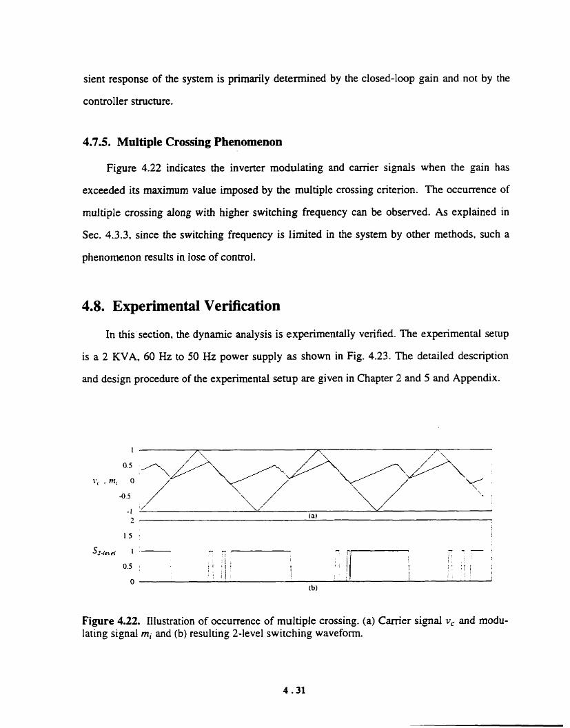
sient response of the system is primarily determined by the closed-loop gain and not by the
controller stmcture.
4.7.5. Multiple Crossing Phenornenon
Figure 4.22 indicates the inverter modulating and cimier signals when the gain has
exceeded its maximum value imposed by the multiple crossing critenon. The occurrence of
multiple crossing dong with higher switching frequency can be observed. As explained in
Sec. 4.3.3, since the switching frequency is limited in the system by other methods, such a
phenornenon results in lose of control.
In this section, the dynamic analysis is experimentally verified. The experimental setup
is a 2 KVA, 60 Hz to 50 Hz power supply as shown in Fig. 4.23. The detailed description
and design procedure of the experimental setup are given in Chapter 2 and 5 and Appendix.
Figure 4.22. Illustration of occurrence of multiple crossing. (a) Carrier signal v, and modu- lating signal mi and (b) resulting 2-level switching waveform.

Le-29 rnH 1 ~ 2 0 A
I = I W
~ I S V . M ) H ~ - -
\\ 11 ( C T 2 KVA
SUPP~Y 4 1 ? 110V. 50 Hz
4 -1 RL Load
c,= IOOpF
Figure 4.23. Power circuit structure and components size of the experimental setup.
Figure 4.24 shows the transient response of the front end rectifier to 70% step load
change. Both experimental and simulation results are obtained under the sarne conditions and
shown on the same scales. The controller gain in this test has been intentionally reduced in.
order to slow down the transient.
Shown in Fig. 4.25 is the invener transient response to 70% load change. Again the
conditions for both experimental and simulation are the same. The close agreement between
the results verifies the analysis.
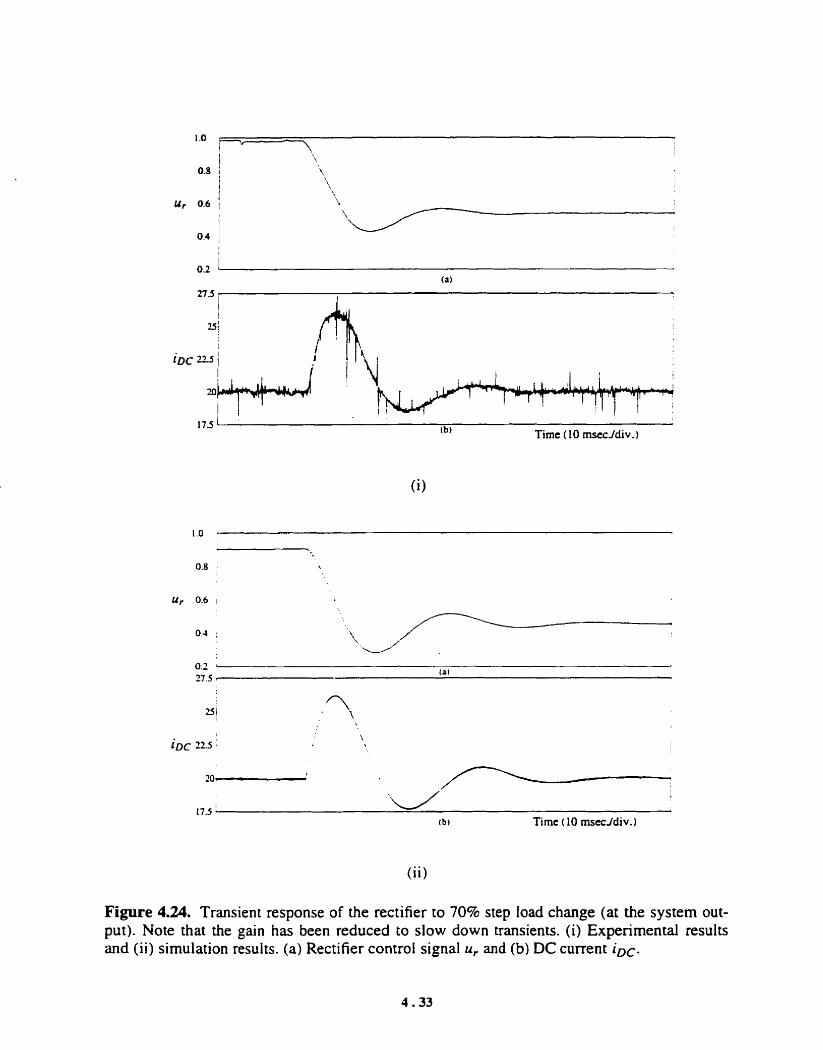
Timc ( 1 O msecldiv .
0.2 (ai
77.5 1
( i i )
Figure 4.24. Transient response of the rectifier to 70% step load change (at the system out- put). Note that the gain has been reduced to slow down transienü. (i) Experimental results and ( i i ) simulation results. (a) Rectifier control signal u, and (b) DC current iDc
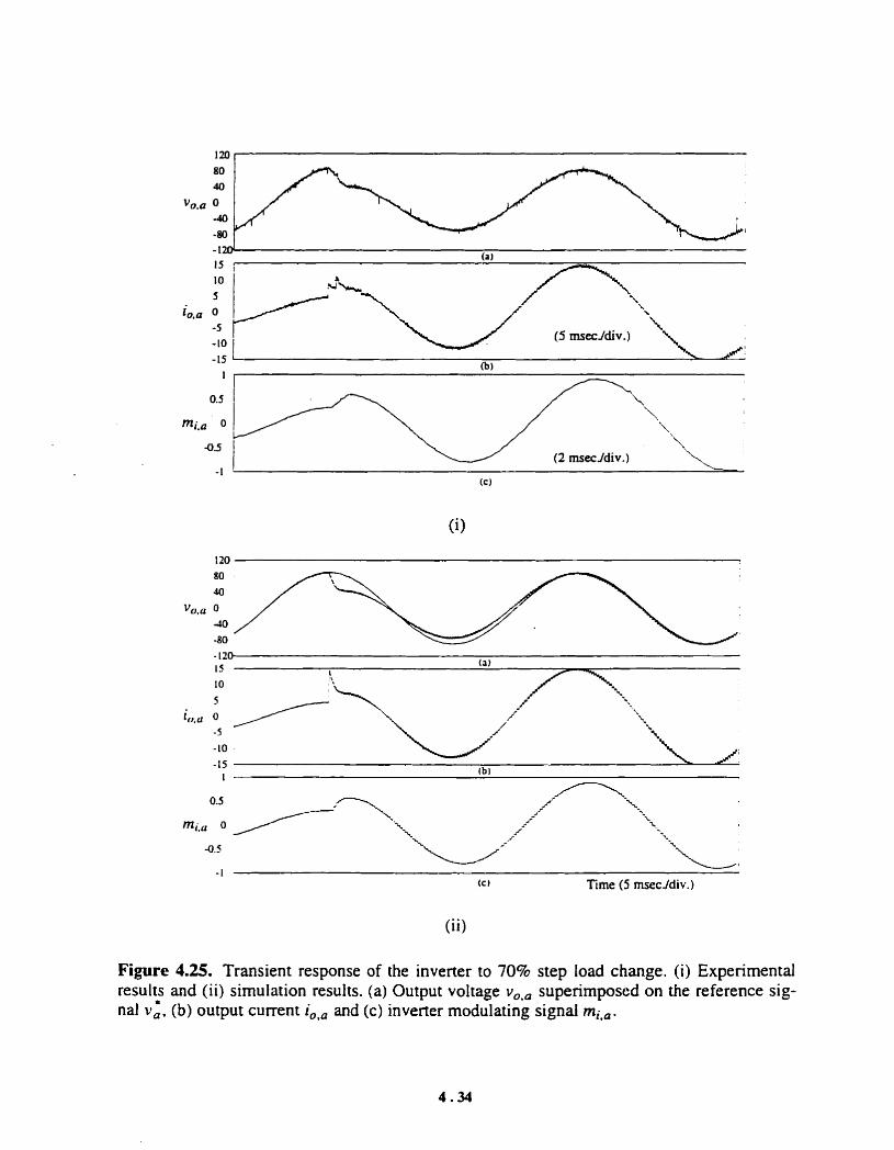
- 1 --p. -p.
(c Time ( 5 msecldiv.)
Figure 4.25. Transient response of the inverter to 70% step load change. ( i ) Experirnental results and (ii) simulation results. (a) Output voltage v,,, superimposcd on the reference sig- nal v i . (b) output current i,,, and ( c ) inverter modulating signai mi,,.

CHAPTER 5
DESIGN OF A CURRENT LINK AC TO AC
POWER SUPPLY
Introduction
The objective of this chapter is to develop a systematic design procedure for a three-
phase current link AC to AC power supply based on the anaiysis presented in Chapters 3 and
4. Two illustrative examples are presented to highlight various aspects of system design.
A linearized mode1 of the inverterlrectifier was obrained in Chapter 4. The agreement
between the dynamic behavior of the linear average models and actual switching systems
was also illustrated. In this chapter, root-locus approach is employed for the design of
rectifierlinverter control systems. In this approach. the loci of closed-loop poles are attained
in s-plane as a selected parameter varying and thus the impact of that parameter on the sys-
tem modes is investigâted.
The implementation of control law in the expenmental setup is perfomed using a
discretized method. Such a method results in a sampled-data system in nature. The cntena
for selection of sampling rate and its correlation with system gain are discussed. Further.

this method imposes additional constraints on the system design by introducing inherent time
delay in the systern response. Therefore, the exact single phase model derived in Chapter 4
has to be used.
Al1 the simpliQing assumptions mentioned in Sec. 3.1 and 4.1 also hold in this chapter.
Specificaily, the design is performed based on loss-less assumption.
The content of this chapter is organized as follows:
In Sec. 5.1, the design criteria are rnentioned in terms of some general qualitative per-
formance specifications.
Section. 5.2 gives the design procedure, including steady-state design for calculating
the size cf components, formulation of transfer hinctions, s-domain design and rime-domain
verification.
A design example for a 400 KVA 60 Hz to 50 Hz power supply is presented in Sec. 5.3.
The design procedure is examined in detail and the controllers are designed using the root-
locus method. The application of approximate single phase mode[ is shown. The design is
verified by time-domain simulation.
In Sec. 5.4, the design of experimental senip is presented in detail. The criteria for
selecting sarnpling rate for discretization of the original system are rnentioned. The necessity
of using exact single phase model is shown. The modeling of time delays introduced by the
controllers is described. The design is theoretically and experimentally verified.
5.1. Design Criteria
The quantitative design criteria are dependent on the systern applications. However.
general qualitative performance specifications c m be proposed for the system as follows:

(i) The system should be stable under dl operating conditions.
(i) The transient response of the system to various disturbances should be made as fast as
possible.
(iii) The steady-state error should be zero.
5.2. Design Procedure
This section gives a systematic procedure for the design of a current link AC to AC
power supply. The procedure is divided into three parts:
( 1 ) Calculation of steady-state system parameten and size of components.
(2) Design of rectifierhnverter controller based on root-locus method.
(3) Time-domain verification.
The following gives the detailed procedure of the design.
5.2.1. Calculation of Steady State System Parameters
The controller design and formulation of system transfer functions are based on the
knowledge of the steady-state system parameters. Therefore, the steady-state design is per-
formed as the first step in the design procedure.
Step 1: Determinhg Base Quantities For Pemnit Calculations
Since most expressions are given in permit basis, the base quantities for the system to
be designed must be determined.
Step 2: Selection of Switching Frequency and Frequency Modulation Ratio
The first parameter to be selected in the system design is the switching frequency of the
converters. The maximum switching frequency of semiconductor devices is nomally deter-

mined with respect to their switching characteristics, namely mm-on/tum-off times. The fre-
quency modulation ratio of each converter is then calculated based on the maximum switch-
ing frequency and employed PWM method. Chapter 2 gives the relevant information in this
context.
Step 3: Selection of Output Filter Configuration
The steady-state system parameters are generdly dependent on the output filter
configuration. If an isolating transformer is employed for isolation of input/output lines, then
proper voltage matching is also possible. If the isolation of input/output terminais is not
required, then voltage matching might not be necessary provided the difference between the
amplitude of input/output voltages is not far from unity. Thus, the next step in the steady-
state design is to identify the necessity of isolating transformer. Section 3.6 provides the
basic guidelines for selection of isolating transformer at the system output.
Step 4: Inverter Output Filter Design
The size of invener output capacitor size is determined based on total harmonic
tion of the output voltage and inverter frequency modulation ratio. Equation 3.16 or
distor-
3.48 is
used for this purpose depending on the output filter configuration. In case of using isolating
transformer, the size of rnagnetizing inductance of the transformer is calculated using Eqn.
3.35.
Step 5: Calculation of DC Current Amplitude
The amplitude of DC current is calculated using Eqn. 3.52 or 3.53, depending on the
output filter configuration.
Step 6: Rectifier Input Filter Design
The size of rectifier input filter is detemined based on total harmonic distortion of the
supply current and the rectifier frequency modulation ratio by using Eqn. 3.20 or 3.2 1. The

rating of the associated cornponents is also obtained using the expressions derived in Sec.
3.2.4.
Step 7: Intermediate DC füter design
The size of intermediate DC filter is calculated based on Eqn. 3.83 and with respect to
the maximum allowable ripple current in the intermediate link. The peak to peak ripple
current is norrnally selected such that the steady-state characteristics are not deteriorated.
5.22. Controiier Design
The controller design begins with the formulation of transfer functions. The main pan
of controller design, however, is the calculation of controller parameters.
Step 8: Formulation of Trader Functions
The rectifier open-loop transfer function is obtained based on Fig. 4.7 as
where VI*, is the r m s value of the supply iine voltage, LDc is the inductance of the intermedi-
ate DC filter and RDc is the resistance of the intemediate DC filter. The transfer function of
the rectifier controller is given by
where Kr and r, are the rectifier controller parameters to be calculated.
S imilarl y, the open-loop transfer function of the inverter single phase approximate
mode1 can be obtained based on Fig. 4-13 as
where IDc is the magnitude of DC current and Gi is the transfer function of the output filter
and load given by Eqn. 4.19. If the exact single phase mode1 is to be used. then based on Fig.

4.16 the open-loop transfer function of the inverter is given by
where D ( s ) is given by Eqn. 4.22. The transfer function of the inverter controller is given by
where mi is the output frequency and ao, a 1 and Ki are the inverter controller parameters to
be caiculated.
Step 9: Calculation of Controllers Parameters
In this step, the root-locus method is employed to inv estig ate the effect
parameters on the ciosed-loop poles. The detailed procedure of parameter selection will be
discussed in design examples.
5.2.3. Time Domain Vedication
The s-domain design is exarnined by time-domain simulation of the linear transfer hnc-
tions. This design is eventually verified by tirne-domain simulation of the acmal switching
system. Funher. these simulations are used to verify the steady-state performance
specifications. The tirne-domain simulation of the actual switching system is performed
using a cornputer program specificall y developed for this research work.
5.3. Design Example 1
This section gives an example for the design of a 400 KVA 60 Hz to 50 Hz power sup-
ply. The design citena are given as foliows:
Output: three-phase 480 V M.58. 50 Hz, THD 5 1 8

Rated power: 400 KVA, unity to 0.8 lagging power factor
Input supply: 1 MVA. 460 V f 10%. 60 Hz
0 Maximum input current distortion: 4 5% (in the supply basis)
Input supply Short Circuit Ratio (SCR): IO (in the supply basis)
Based on the given specification for the serniconductor switches, the average switching
frequency (Sec. 2.3.2) should not exceed 7.5 KHz.
5.3.1. Calculation of Steady State System Parameters
Step 1: Determining Base Quantities For Perunit Calculations
The system base values are given as
S&00 KVA
V&80 V
Step 2: Selection of Switching Frequency and Frequency Modulation Ratio
Assuming the rectifier has sawtooth carrier. then its carrier frequency is selected to be
14940 Hz. which based on Eqn. 2.19 results in switching frequency equal to 7470 Hz and
frequency modulation ration equal to 249. Similarly, assuming the inverter employs triane-
Iar carrier, its carrier frequency is selected to be 7350 Hz, resulting in the same switching fre-
quency and frequency modulation ratio of 147.
Step 3: Selection of Output Filter Configuration
In this design example. the amplitude of input/output voltages are close together. Thus,
based on the discussion given in Sec. 3.6, an isolating transformer is not necessary for the

voltage rnatching.
Step 4: Inverter Output Füter Design
Using Eqn. 3.47, the size of output capacitor is calculated as
Xc=2.96 perunit
=l.72 i2
giving
C=1850p F
Step 5: Caiculation of DC Current Amplitude
Since no isolating transformer is employed at the system output, then based on Eqn.
3.52 the.DC current amplitude is given by
= 1.724 perunit
giving
bc=830 A (5.9)
To check the necessity of isolating transformer for voltage matching, the maximum average
value of the inverter input DC voltage is calculated based on the power balance in the system
V ~ ~ . i . m a r I ~ ~ = P o u i . m a r
giving
v ~ c . i ,mar=482 (5.1 1) Based on lossless analysis. the rectifier must be able to maintain this average voltage under
wont operating condition. which is 108 undervoltage. Based on Eqn. 3.70, this value is cal-
culated as
giving

v ~ ~ . r.mar'507 v which is greater than VDCi,-, and thus the primary assumption is vaiid.
Step 6: Rectifier Input Filter Design
Based on the Short Circuit Ratio (SCR) of the input supply, its intemal impedance is
0.1 perunit in the supply basis. which is equal to O. lx 400 KVA = 0.04 pemnit in the system 1 MVA
basis. Sirnilarly, 5% harmonic distortion in the supply basis is equal to
1 MVA 5%~-- = 12.5% distortion in the system basis. Now substituting the numerical 400 KVA
values based on the given specifications into Eqn. 3.20 yields
giving
or
Xc=401 perunit
=232 R
Step 7: Intemediate DC Filter Design
The peak to peak ripple current in the intermediate DC link is chosen not to exceed 5 6 .
Thus. substituting the numerical values into Eqn. 3.83 and solving for XDc yields
giving
Figure 5.1 indicates the power circuit along with the steady-staie parameters.

Figure 5.1 Power circuit dong with size of components for Design Exarnple 1 .
5.3.2. Controller Design
Step 8: Formulation of Transfer Functions
Based on Eqn. 5.1. the rectifier open-loop transfer function is obtained as
It will be shown shonly that the single phase approxirnate mode1 is satisfactory for the
design of inverter controller in this example. Thus. the inverter open-loop transfer function is
obtained using Eqn. 5.3 as
Step 9: Calculation of Controllers Parameters
The rectifier and inverter are considered separately in this step.

(i) Rectifier Controller Design
There are two parameters to be calculated in the rectifier PI controller. narnely the con-
troller gain Kr and time constant t,. In this design example, the gain is set to its maximum
value limited by the multiple crossing phenomenon, and then the time constant is calculated.
Substituting numerical values in Eqn. 4.15 yields
giving
Kr < 0.014 (5.22)
Thus, the rectifier gain is set to 0.013. The selection of controller time constant is trivial. and
it is set to 0.00 1.
(ii) Inverter controller design
It was observed that the single phase approximate mode1 provides acceptable results in
design of inverter control system. and thus it is used in this design example. There are three
parameters to be calculated in the inverter control system design, narneiy Ki. a and a 0. As
in the rectifier case, in this design the gain is caiculated and fixed based on the constraint
imposed by the multiple crossing phenomenon. and the coefficients of the controller nurnera-
tor are calculated consequently. In doing so. therefore. the mot-locus is plotted versus the
variation of zeros instead of variation of gain.
Substituting numerical values in Eqn. 4.3 1 yields
giving

Ki < 0.051 (524) In the following design course. the controller gain is set to 0.05. Note that practical con-
siderations such as noise may further limit the controller gain. Nevertheless. the design
approach is the same.
Before calculating the controller parameters. it is worth noting that while the poles are
the inherent part of the inverter controller based on the discussion presented in Sec. 4.42. the
controller zeros are incorporated for adequate system performance. To illustrate this, con-
sider Fig. 5.2 in which the root loci are plotted venus gain when the controller has no zero
and one zero respectively. As can be seen, the system is unstable in both cases.
. To inspect the effect of controller zeros on the system root-locus, the controller transfer
function is re-written as
In this way, the Iocation of zeros and their impact on the root-locus cm be better realized and
investigated. Figure 5.3 shows the root-loci versus z 1 with zz as the parameter for different
combination of controller zeros. Concerning these loci. the following notes can be made:
The higher the magnitude of the zeros. the farther the closed-loop poles from the ima-
ginary axis, and hence the faster the transient response.
If the magnitude of both zeros are greater than about 3000. two complex poles appear in
the closed-loop system. The damping of these poles decreases as the zeros become
larger.
One low magnitude zero always results in a slow mode. However, it was observed that
if the magnitude of other zero is large. then the ratio of the residue to the pole for this
mode is relatively smaller than those of faster modes. and thus the impact of slow mode
is insignificant.

Figure 5.2 Invener closed-loop root-locus when (a) the controller has no zero and gain varies from O to 0.05 and (b) the controller has one zero which varies from -100 to -500 and the gain is fixed to 0.05.

(a) zl=-100, z2= -100 to -5000
-2500 a -2 -1.5 - t -0.5 O
Real x 10'
(e) ;l=-lOûû, z2=- lûû to -5000
8 -
6 -
4 -
2 -
,E O .
-2
4-
4-
-8-
-101 -1MO - t 000 -500
Real
I
K - -
I
(0 ; -1 000, z z= - 100 to -5000 (expanded)
-'& -1 50 -100 -50 O Real
(b) z 1=-10(l, r z= - 100 to -5000 (expanded)
Figure 5.3 Root-loci of the invener control system for different combinations of controller zeros when the gain is fixed. "O" and "x" signs show the start and end of the locus respective- IY.

( i ) zl=-5000, z7= -100 to -5000
Figure 5.3. (Continued)
Choosing complex conjugate zeros has no particular advantage on the system response.
The above observations demonstrates that large zeros generally provide better transient
perfomance. On the other hand. if the magnitude of both zeros is selected to be high. Say
greater than 3000, then the system becomes unstable for small gains. This is illustrated in
Fig. 5.4.a in which the root-locus is piotted versus the gain with hvo large zeros at s=-6000
and s=-8000. This instability does not exist when the magnitude of just one zero is high.
The final selection will be made after examination of time domain response of the linear

o O -eo'oo -6Wo -40'00 -2000 1
O Real Axis
Figure 5.4 Root-locus versus gain when the magnitude of both zeros is larger than about 3 0 . The instability for srnail gains can be observed.
transfer functions.
5.3.3. T h e Domain Verification
In this section. the s-domain design is venfied by cime-dornain simulation of the actual
switching system. In this way. first the s-domain design is examined by illustrating the simu-
lation results of the linear transfer functions.
Figure 5.5 illustrates the response of the invener average model to the step load change
with different combination of controller zeros. As expected. when both zeros are small. the
transient response is relatively slow (Fig. 5.5.a). If the magnitude of one zero is increased.
the effect of slow mode alrnost disappears (Fig. 5.5.b). As the magnitude of zeros increases.
the transient response becomes faster (Figure 5.5.c to 5.5.f).

On the other hand, inspection of Fig. 5.5 shows that as long as the amplitude of one
zero is large, Say greater than 2000. then the transient response of the system does not
significantly change with the variation of zeros. An important result of this observation 1s
that the system is robust with respect to the controller parameter variation.
Based on these observations, the conuolier zeros are selected to be ; 1 = -300 and
z 2 = -3000. This ensures stable operation in al1 operating conditions and satisfactory tran-
sient response.
Figure 5.6 illustrates the transient response of both exact and approximate single phase
models. It can be seen that the general dynamic behavior of both system is the sarne. show-
ing that the approximate mode1 is satisfactory for design purpose.
The final step in verification of controller design is the cornparison benveen the s-
domain results and tirne-domain simulation of the actud switching system. In this way, the
validity of modeling is also venfied. Figure 5.7 shows the transient response of the system to
k100% step load change. The fast transient response and negligible voltage distortion can be
observed. Shown in Fig. 5.8 is the expanded transient response of the inverter to step load
change ( 1 R = 1.73 permit resistive load) for both linear average mode1 and actual switch-
ing system. The gain in this test has been reduced to 0.01 in order to slow down the tran-
sients. The agreement between results shows the validity of rnodeling.
As stated in the beginning of this section. the time domain verification is also used to
examine the steady-state design. Table 5.1 shows the cornparison between the predicted and
rneasured steady-state results. The close agreement verify the vdidity of analysis and design.

(a) z , =- 100, z *= -200
Timc ( 1 rnsccldiv.)
i'
Tirne ( 1 rnsccldiv.)
Time ( 1 msecldiv.i
Y
Time ( 1 msecldiv.)
Figure 5.5 Transient response of inverter average linear mode1 to a step load change for dif- ferent combinations of zeros.

Figure 5.6 Cornparison between transient response (shown for error signal) of average and exact single phase models. Top: exact model. Bottom: approximate model.
lm- ( C l
Figure 5.7 System transient response to + 1 0 0 1 step load change. (a) Output voltage v,., su- perimposed on the reference voltage v z . (b) Output current i,,,. ( c ) inverter modulating sig- nal mi,,, (d) DC current iDc and (e) rectifier control signal u,.

-IO Time (0.5 rnsecldiv. )
Figure 5.8 Inverter transient response for the rea! switching system superimposed on the wavefoms obtained from - the average Iinear model. (a) Output voltages v,., and F,,,, (b) output currents i,., and i,,,. (c) modulating signals m,, and mi,, and (d) error signais ei,,
and Ziia-

Table 5.1. Cornparison between predicted and measured steady-state results.
parame ter
Average rectifier out- put voltage ( VDC, r)
- -- -- - - --
Average inverter in- put voltage ( V D c i )
Amplitude of the first dominant harmonic in the inverter output current (li,mf&i )
Amplitude of the first dominant harmonic in the inverter input vol- tage (VDC, i,mf&3 )
Output voltage. distor- tion ( T m V )
Inverter fundamen ta1 output current (Ii* 1 )
482 V (Eqn. 3.68)
cakulation
490 V (Eqn. 3.68)
3 1.8% (Eqn. 3.38)
theore tical verification
487 V
176 V (Eqn. 3.60)
1 % (Eqn. 3.47)
715 A (Eqn. 3.36)

5.4. Design Example 2: Experimental System Design
In this section, the design of experimental system is presented. The detailed structure of
the experirnental setup is given in Chapter 2 and Appendix A. The system specifications and
the design cntena are as foliows:
Output: three-phase 110 V +0.5%, 50 Hz, THD S 3%
Rated power: 2 KVA, unity to 0.8 lagging power factor
Input supply: three-phase, 1 15 V, 60 Hz
Measured supply impedance: 40 pH
Maximum input current distortion: 15% (in system basis)
Switching frequency : 1 5 KHz.
The rated power was selected based on the rating of the components in the experimental
setup. The switching frequency was selected based on the given specifications of the sem-
iconductor switches and existing snubber circuits.
5.4.1. Calculation of Steady State System Parameters
Step 1: Determining Base Quantities For Perunit Calculations
The base values are caiculated as
SB=? KVA
V,=llO v

S e p 2: Selection of Switching Frequency and Frequency Modulation Ratio
As discussed in Chapter 2. both the inverter and rectifier in the experimental setup use
the same carrier signal. The frequency of the carrier is synchronized with respect to the
inverter fundamental frequency, and thus the rectifier operates in free running mode. Le. rn f - ,
is not an integer. Despitethat, the calculations performed in Chapter 3 are still valid with
acceptable accuracy. Now based on the given critenon for the switching frequency, the fre-
quency modulation ratio for the inverter is selected to be 99. This results in carrier frequency
equal to 4950 Hz.
Step 3: Selection of Output Fiiter Codguration
The experimental setup was implemented without using isolating transformer because
the amplitude of inputfoutput voltages are close together.
Step 4: Inverter Output Füter Design
Using Eqn. 3.47, the size of output capacitor is calcuiated as
Xc=6.24 pemnit
giving
The CIO
Step 5:
sest value is 100 pF which results in THDv equal t
Calculation of DC Current Amplitude
Since no isolating transformer is employed at the system output, then based on Eqn.
3.52 the DC current amplitude is given by

giving
IDc=17.8 A (5.29)
To cover the losses, the DC current is selected to be 10% higher, and thus is set to be 20 A.
Step 6: Rectifier Input Filter Design
Selecting the input filter capacitor to be 100 pF and substituting into Eqn. 3.30 yields
giving
A portion of input filter inductance equal to 40 pH presents in the Iine. The res
(5.3 1 )
t of the
required inductance is provided by a 100 pH three-phase inductor. Recalculating Eqn. 5.31
results in THDI to be equal to 7%.
Step 7: Intermediate DC Filter Design
The peak to peak ripple current in the intermediate DC link is chosen not to exceed 5%.
Thus. substituting the numerical values in Eqn. 3.79 and solving for XDc yields
XDc= 1 -5 petunit (inverter base)
=9.1 R giving
5.4.2. Controller Design
As stated in Chapter 2, the controllers in the experimental setup are designed in ccn-
tinuous time (Le. in s-domain). but are digitally implernented using a DSP-based digital con-
troller. This approach. described in Appendix A. is sometimes called emulation method. as
opposed to direct digital design.

The emulation method resulü in a sampled-data system [15]. For proper design of such
a system, the following important factors are to be taken into consideration:
( 1 ) The sampling frequency used in the controller discretization should be well higher than
the system bandwidth in order to have satisfactory agreement between the dynarnic
behavior of original and discretized systems. As a mle of thurnb. a factor of at leas 10
ensures this requirement. On the other hand. the maximum sarnpling frequency in a
digital controller is practically restricted [34]. Moreover, the switching frequency is
also a function of sampling frequency in the employed control scherne. These interre-
lated pararneters make the choice of sampling frequency very crucial.
(2) The digital controller holds the controller output until the next data anives. This is
analogous to a zero order hold action. Sampled data systems with zero order hold at the
output produce an inherent time delay equal to T'/2 in the system [15], where Ts is the
sarnpling period. Furthemore. the data transfer mechanism creates an additional delay
equal to one sampling period. as explained in Appendix A. The mentioned time delays
should be properIy taken into consideration.
Based on the above mentioned factors, and to take into account the effect of new
pararneters associated with the impiementation of controllers. the following steps are to be
foIlowed:
( 1 ) The sampling frequency should be selected primarily with respect to the hardware and
software limitations. Generally speaking. the higher the sarnpling frequency. the higher
the system bandwidth. and the faster the transient response. After selection of sampling
frequency. the system gain should be calculated accordingly. The sarnpling frequency
is usually more burdensome than the multiple crossing phenornenon in calculation of
controIler gain.
(2) The time delays associated with the zero order hold and data transfer rnechanism should
be properly taken into account. A common method is to mode1 the time delay by a

transfer function and incorporate it in the original continuous model [15]. The total
time delay associated with the system discretization is equal to TsR + Ts = 3 7 ' 3 . This
time delay is modeled by a first order transfer function given by [x]
It was observed that this step is very crucial in design of the inv
( 5 -34)
erter control system,
however, it can be skipped in the rectifier control system design due to its simple struc-
ture.
(3) For the design of inverter control system, and for low sampling frequencies in which
time delays are significant. the single phase approximated mode1 does not con-ectly
represents the dynamic behavior of the actual switching system. Therefore. the exact
single phase modei must be used in the design of inverter control system.
(4) Al1 the s-domain designs should be eventually verified by time-domain simulation.
To illustrate the significance of the above mentioned factors. the design of invener con-
trol system in the experimentai setup was performed using the following modeis:
( i ) The single phase approxirnate mode1 shown in Fig. 4.15.a with time delay.
( i i ) The single phase exact model shown in Fig. 4.16 without time delay.
(iii) The single phase exact model shown in Fig. 4.16 with time delay.
Table 5.2 shows the inverter closed-loop poles corresponding to three models with
sirnilar controllers. The controller parameters are intentiondl y selected such that the actual
sampled-data system is unstable. It can be seen that only the third model demonstrates this
instability, i.e.. other models cannot precisely represent dynarnic system behavior.

Table 5.2. Closed loop poles of the inverter control system for three different models with
approximate single phase model with tirne delay
exact single phase mode1 without time delay
exact single phase mode1 with tirne delay
On the other hand, the mentioned factors do not have a significant impact on the
rectifier control system. Therefore, the mentioned considerations are taken into account only
for the inverter control system in the experimental senip..
Based on the performance of the digital controller. the sampling frequency was selected
equal to the switching frequency. i.e. 4950 Hz. Therefore based on the above mentioned cri-
teria. the bandwidth of the inverter control systems has to be 500 Hz or less.
The modified block diagrarn of the invener control systems including the time delay
transfer function is shown in Fig. 5.9. Based on the maximum system bandwidth. the con-
troller gain is cdculated to be less than 0.005.
Using root-locus approach. the controller design can be camed out in a similar way
explained in Design Example 5.1. Figure 5.10 shows the root-locus of the dominant poles in
the inverter control system versus the variation of one zero when the gain and other zero are
fixed. After examining different combination of zeros, they are selected to be z 1 = -200 and
z z = -300.

Figure 5.9 Exact single phase block diagram of the inverter control system including time delay associated with digital conuoller.
Figure 5.10 Expanded root-locus for the inverter control system when Ki = 0.005. c 1 = -200 and ; 2 varies between - 100 and - 1000.

5.4.3. Time Domain Verification
In this section, the s-domain results are verified by time domain simulation of the acnial
switching system. Figure 5.1 1 .a and 5.1 1 .b show the results obtained from the time-domain
simulation of the linear transfer functions (s-domain results) and the actual switching system
respectively. The agreement between results shows the vdidity of modeling. The steady-
state and dynamic experimental results are shown in Chapter 3 and 4 respectively.
-20 Time (5 msecjdiv.)
Figure 5.11 Inverter transient response for the linear average mode1 (top) and real experi- mental system (bottom).

CHAPTER 6
CONCLUSIONS
In this thesis, a comprehensive snidy of the analysis. design and expimental
verification of a current link AC to AC power supply has been presented. This subject has
not been properly explored in the literature. Considering the decreasing prices of power
semiconductor devices. the cost of power electronic systems is dominated by magnetic corn-
ponents. It has been shown here that the proposed configuration has a smailer number of
magnetic components and therefore is Iess costly as cornpared to other configurations.
Further, it has been proved that this approach is a practical and reliable method for building
an AC to AC power supply with sinusoidal input/ourput current.
The main contributions and conciusions of this thesis may be summârized as follows.
1. The restrictions existing in PWM pattern generation in three-phase current type con-
verten have been identified and expressed in a simple manner. Three conceptually dif-
ferent PWM methods have been explained, and their performance in ternis of open-loop
and closed-loop charactenstics, switching frequency and low frequency hmonics have
been identified. It has been shown that the SIN-PWM method with triangular carrier has
the best perfomance for high quality low distortion output voltage. The SIN-PWM
technique and its on-line implementation in the proposed system has been described.
2. The steady state modeling and analysis of the system have been presented. The steady
state relationships between fundamental components of AClDC currents and voltages in

a CTC have k e n derived. The PWM wavefom have been represented by their
corresponding Fourier series for precise filter design. Closed f o m expressions and
graphs have been provided to simplify the design. The analysis has ken carried out
both for a system without and a system with isolating transformer at the output. The
impact of output isolating transformer with tuned magnetizing inductance on system
rating has been discussed.
3. A systematic dynamic modeling has been presented based on the concept of local aver-
age of signais. It has k e n shown that, by using this method, a nonlinear switching sys-
tem cm be modeled by a linear system having similar dynamic characteristics. Close
agreement between the actual switching system and the linear models has been illus-
trated. The approxirnate and exact single phase models have been obtained. The appli-
cability of each model in a specific design example has k e n discussed. The interpreta-
tion of bandwidth in the linear model and actual nonlinear switching system has been
explained.
4. The concept of interna1 model controlier has been introduced and employed in the
design of inverter control system. It has been demonstrated that unlike conventional
controllers in tracking control systems, the proposed controller can provide zero steady
state error for al1 operating conditions irrespective of the controller gain.
5 . A systematic design procedure for current link AC to AC power supply systems has
been developed. The time delay associated with digital implementation of the conaoll-
ers has been identified and the associated modification in the original model has been
suggested. The impact of this time delay on the closed loop system design has been
shown. The correlation between sampling frequency and system design has been

explained
6. A 2 KVA, 60 Hz to 50 Hz experimental setup has been implemented in the laboratory
with a high performance DSP-based digital controller. After proper modeling and sys-
tem design, al1 the control laws have k e n discretized and then realized by the above
mentioned digital controller. Redicted steady state and dynarnic results have been
experimentally verified.
The future work is suggested as follows:
1. The feasibility of implernentation of the proposed system was expenmentally verified in
this thesis at low power level. Various aspects of high power systerri implementation
need to be investigated.
2. The proposed configuration needs switching ce11 with the capability of reverse voltage
blocking. Currently. such a switch is not commercially available, and hence has to be
implemented using an IGBT and a series diode. A matched pair of IGBT and diode is
expected to have better performance specidly at high current levels.
3. The proposed configuration can potentially have a wide application in systems such as
variable frequency AC drives. The control system for these applications should be
investigated.
4. Regenerative operation of the system needs to be investigated. The focus in this thesis
is on power supply applications where the regenerative operation is not required. For
applications such as parallel processing power supply systems. however, the system
must operate in regenerating mode. Thcrefore. the control strategy and dynamic
behavior of the system in this mode should be studied.

5. A sustained oscillation is observed if the damping in the input filter is not sufficient.
Use of an active damping scheme to bnng these oscillations under control without
excessive losses should be Iooked into.

[ l ] IEEE Std. 5 19-1992, "Recornmended Practices and Requirements for Harmonic Con-
trol in Electrical Power Systems".
[2] A. Alesina, and M.G. B. Venturini, "Analysis and Design of Optimum-Amplitude
Nine-S witch Direct AC-AC Converters," IEEE Trans. Power Electronics, vol. PE-4,
no. 1, pp. 101; Jan. 1989.
[3] M. Venturini, "A New Sin Wave In, Sin Wave Oui, Conversion Technique Elim-
inates Reactive Elements," inProc. Powercon 7, San Diego, Ca, 1980, pp. E3-bE3-
15.
[4] L. Huber, and D. Borojevic. "Space Vector Modulation With Unity Power Factor For
Forced Commutated Cycloconvenen," in IEEE IAS Annual Meeting. 199 1 , pp.
1032-1041.
[5] R. R. Beasant. W. C. Beattie, and A. Refsum, "An approach to the Realization of a
High-Power Venturini Converter." IEEE Power Electronics Specialists Conference
Record (PESC), 1990. pp. 291-297.
[6] R. Wu, S . B. Dewan, and G. R. Slemon. "Anaiysis of an AC-to-AC Voltage Source
Converter Using PWM wi th Phase and Amplitude Control," IEEE Trans. Ind. AppL,
vol. LA-27, no. 2. pp. 355-364. 199 1.
[7] B. T. Ooi. J. C. Salmon. J. W. Dixon. and A. B. Kulkarri, "A 3-phase Controlled
Current PWM Convener With Leading Power Factor," in IEEE IAS Annual Meeting.
1985, pp. 1008-1014.

L. Moran, P. D. Ziogas, and G. Joos. "Design Aspects of Synchronous PWM
Rectifier-hverter Systems Under Unbdanced Input Voltage Conditions." in IEEE
IAS Annual Meeting, 1989, pp. 877-884.
A. Tripathi, S.B. Dewan. "Modeling And Design of a Novel Voltage Control System
For Three Phase Fixed Frequency Static Power Supplies." in IEEE IAS Annual
Meeting. 1 995, pp. 264 1 -2645.
L. Gyugyi and E. C. Strycula, "Active AC Power Filters," in IEEE IAS Annual
Meeting, 1976, pp. 529.
H. Akagi, A. Nabae, and S. Atoh, "Control Strategy of Active Power Filters Using
Multiple Voltage-Source PWM Converters," IEEE Trans. Ind. Appl.. vol. IA-22. no.
3, pp. 460-465 1986.
S. M. Williams. and R. G. Hoft, "Irnplementation of Current Source Inverter for
Power Line conditioning," IEEE Trans. Ind. AppL., vol. IA-27, no. 4. pp. 773-779
1991.
M. Iwahori and K. Kousaka. "Three-phase current source GTO rectifier adopting new
PWM control techniques", in IEEE IAS Annual Meeting. 1989, pp. 855-860.
L. Malesani and P. Tenti, "Three-phase AC/DC PWM converter With SInusoidal AC
Currenü and Minimum filter Requirements." IEEE Trans. I d Appl., vol. IA-23, no.
l.pp.71-77, 1987.
G. F. Franklin. J. D. Powell. and A. emami-Naeini, "Feedback Control of Dynamic
Systems," Third Edition. Addison-Wesley Publishing Co.. 1994.
B. A. Francis and W. M. Wonham, "The Interna1 Mode1 Pnnciple of Control
Theory," Automatica. vol. 1 2. pp. 457-465, 1976.

J. C. Doyle, B. A. Francis, and A. R. Tannenbaum, "Feedback Control Theory."
Maxwell Macmillan International, 1992.
S. Krebs, "UHP40 User's Manual," University of Toronto, Dec. 1995.
J. Hola. "Pulsewidth Modulation - a survey," IEEE Trans. Ind. Electronics. vol. IE-
39, no. 5, pp. 410-420, Oct. 1992.
C. Namuduri, and P.C. Sen, "Optimal pulse width modulation for current source
inverters," IEEE Trnns. Ind. AppL, vol. IA-22, no. 6, pp. 1052-1072
~ovemberl~ecember 1986.
"IGBTMOD and lntellirnodM - Intelligent Power Modules Applications and Techni-
cal Data BOOK," First Edition, Powerex, Inc., 1994.
Toronto, Dec. 1995.
M. Pande, "Design of a Fast Quad Channel AfD Converter Board," uni ver si^ of
and
Altera Data Book, Altera corporation, 1995.
H. S. Patel and R. G. Hoft. "Generalized Techniqi ies of Harrnonic Elimination
Voltage Control in Thyristor Inverters: Part 1 -Harmonie Elimination." i E E Trans.
Ind. Appl.. vol. iA-9, no. 3, pp. 3 10-3 17, 1973.
B. Wu, S. B. Dewan, and G. R. Slemon, "PWM-CS1 inverter Induction Motor
Drives," IEEE Trnns. Ind. Appl., vol. IA-28, no. 1, pp. 64.71, 1992.
H. R. Karshenas, H. A. Kojori and S. B. Dewan, "Generalized Techniques of Selec-
tive Harmonic Elimination and Current Controi in Current Source
Inverters/Converters." IEEE Trans. Power Electronics, vol. PE-IO, no. 5, pp. 566-
573, Sept. 1995.
H. W. Van Der Broeck, H. C. Skudelny, and G. V. Stanke, "Analysis and Realization
of a Pulsewidth Modulator Based on Voltage Space Vectors," IEEE Truns. Ind. Appl..
vol. IA-24, no. 1, pp. 142- 150, 1988.
S. R. Bowes and R. Bultough, "PWM Switching Strategies for Current-Fed Inverter
Drives." in IEE Proceedings, vol. 13 1, Pt. B, no. 5, pp. 195-202, 1 984.
J. A. Houldsworth and D. A. Grant, "The Use of Harmonic Distortion to Increase the
Output voltage of a Three-phase PWM Inverter." IEEE Trans. Ind. A&. vol. IA-20,
no. 5 , pp. 1224- 1227, 1984.
J. W. A. Wilson and J. A. Yeamans, "Intrinsic Harmonies of Idealized Inverter PWM
Systems," in IEEEE IAS Annuul Meeting, 1976, pp. 967-973.
LG. Kassakian, M.F. Sshlecht, G.C. Verghese, "Principles of Power Electronics,"
Addison-Wesley, 199 1.
R. D. Middlebrook and S. Cuk, "A General Unified approach to Modeling Switching
Converter Power Stages, " FIIEEE Power Electronics Specialists Conference Record
(PESC), 1976. pp. 18-34.
P. C. Krause, "Analysis of Electric Machinery." McGraw-hi11 book Co., 1986.
K. J. Astrom and B. Wittenmark. "Computer Controlled Systerns." Printice Hall.
1990.
A. Baronian, "Design of an ATM Interface Board for the PC." University of Toronto.
Dec. 1995.
F. Neukam. "Developement of a Monitor Program under OS-2 WARP for Visualiza-
tion and Test," Diplorna Prijecr. Universi- of TorontdET7, Oct. 1995.
[37] F. Amelink and A. Tnpathi, "Introduction io the DSP-Kemel and the User Interface:
User's Manual," University of Toronto, Dec. 1995.
[38] Altera Corporation, "Max+Plus II Programming Logic Development System: Getting
Started," July 1994.
1391 J.R. Espiniza, G. Joos and P.D. Ziogas. "Voltage Controlled Current Source Inverter."
Conf. Rec. IECON' 92, Nov. 1992, pp. 5 12-5 17.
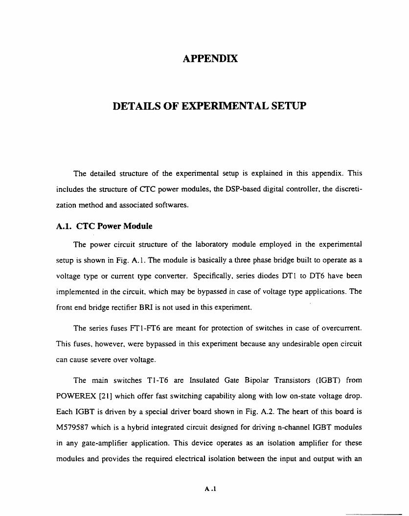
APPENDM
DETAILS OF EXPERIMENTAL SETUP
The detailed structure of the experimental setup is explained in this appendix. This
includes the structure of CTC power modules, the DSP-based digital controller, the discreti-
zation method and associated softwares.
A.1. CTC Power Module
The power circuit stmcture of the laboratory module employed in the experimental
setup is shown in Fig. A. 1. The module is basicaily a three phase bridge built to operate as a
voltage type or current type converter. Specifically, senes diodes DTl to DT6 have been
implemented in the circuit. which may be bypassed in case of voltage type applications. The
front end bridge rectifier BRI is not used in this experiment.
The series fuses FT1-FT6 are meant for protection of switches in case of overcurrent.
This fuses, however. were bypassed in this expenment because any undesirable open circuit
can cause severe over voltage.
The main switches Tl-T6 are Insulated Gate Bipolar Transistors (IGBT) from
POWEREX [21] which offer fast switching capability dong with low on-state voltage drop.
Each IGBT is driven by a special driver board shown in Fig. A.2. The hem of this board is
M579587 which is a hybrid integrated circuit designed for driving nchannel IGBT modules
in any gate-amplifier application. This device operates as an isolation amplifier for these
modules and provides the required electrical isolation between the input and output with an

opto-coupler. Each driver board is supplied by two I l 0 volts isolated power supply.
Other passive components around switching devices are the standard snubber network.
A.2. Digital Controller Unit
As mentioned in Chapter 2, the control unit in the experimental setup is UHP-40 [18]
which is a high performance 32 bit DSP-based digital controller developed at The Power
Group at The University of Toronto. An overall structure of this controller is shown in Fig.
A.3. A bnef description of each block is presented in the following.
The heart of UHP-40 is the DSP TMS32K40 (c40) from Texas Instrument. The inter-
nai structure of c40 is 32 bit for d l address and data paths. Two static RAM modules (Bank 1
and Bank 2) with standard size c m be connected via SIMM-socket to the local bus. At least
Bank 1 is usuaily populated to provide a minimum amount of RAM space. A third RAM
module (Bank 3) is connected in a similar way to the global bus.
The unit has VMEbus interface capability. which is one of the most popular indusmial.
standardized interfaces. The VMEbus circuit uses its own CPU which is the Motorolla
MC68030, The circuit around this CPU consists of another 32-bit wide bus which accesses a
forth SRAM module (Bank 4). Besides Bank 4 an in-circuit programmable Flash-PROM is
also connected to the bus. It uses only 8 data lines but can be directly accessed by the CPU
using its capability of dynamic bus sizing. The SCV64 chip is a complete VMEbus interface
and performs al1 common types of VMEbus transfer cycles and therefore guarantees full
VMEbus compatibility of UHP4O. A dual as y nc hronous receivedtransmitter (DU ART)
with 8 bit bus interface provides a serial RS-232 interface.
UHP-40 has six high speed interfaces called ComPon. The CornPorts provide 8 bit
asynchronous data paths with handshake mechanism. Four of these CornPorts are accessible
through connectors in order to mount up io four AID board directly on the main board [22].
Two CornPorts have additional circuitry to provide an Asynchronous Transfer Interface

(ATM-interface) via HotLink [35] for a reliable, electrically decoupled data transfer over
longer distances to a Personai Computer (PC) or another UHP-40.
In case of a connected PC, prograrns can be downloaded or a prograrn called DSP-
Monitor [36] can be used to visualize incorning data in real time or to adjust parameters on-
line, set desired values etc. The corresponding prograrn on the DSP, which provides a
software interface for the user, is called DSP-Kernel [37] and has k e n optimized in order to
keep the software overhead as low as possible.
UHP-40 has also a Field Programmable Gate Array (FPGA) [23] which c m be directly
accessed via DSP. The main purpose of this chip is the generation of PWM patterns directly
frorn the controller output signals. Since the prograrn for the design of the FPGA algorithm
allows graphicd entry. the user can easily combine the specific design with already available
design modules [38]. Figure A.4 shows two sarnple Graphical Design File (GDF) created by
Max+Plus II [38] software.
Data acquisition in the expenmental setup is perfomed by Analogue to Digital ( A D )
boards custornized for UHP-40 [22] . Each board is mounted on the CornPort sockets and
consists of 4 A/D channels with fast data acquisition capability.
A.3. Control Law Implementation
As discussed in Chapter 5. the design of control system in the experimental setup is car-
ried out using continuous methods. but the implementation of control law is performed by
digital techniques. Therefore. the control system has the structure of sampled data systems.
This method is sometimes called emulation. as opposed to discrete design which is directly
performed in z-domain.

To discretized a continuous time control law, the Bilinear or Tustin's approximation is
employed [15,34]. It cm be shown that substituting
for every occurrence of
tion corresponding to a
(A. 1)
s in any s-domain transfer function yields a z-domain transfer func-
difference equation. Ts in the above equation is the sampling time.
Using this technique, the inverter control law expressed by
'can be written as
from which the corresponding difference equation can be obtained.
The control law wntten by the user is executed by UHP-40 at each sampling time. Upon
the receipt of data via A/D boards at the beginning of each sampling penod, die DSP-Kemel
does necessary initializations and communications with PC. Then the control law is exe-
cuted, and the results are sent to the output with no delay. The bus interface at the FPGA
input. however, stores the data and releases them at the beginning of next sampling perïod.
This results in a synchronized data transfer but leads to a time delay equal to one sampling
period. This delay, in addition to the delay introduced by the sample and hold mechanism,
should be properly taken into consideration in the system design.
The listing of the associated software is included at the end of appendix.
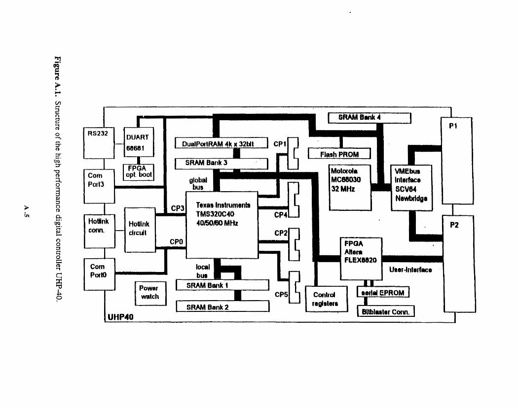
Cm* - drcuit CP2 CPO I
I *
Corn Porto
b POWO~
I

Figure A.2. (a) Block diaagaam of the IGBT driver boards and (b) internai circuitry of M579587.

Figure A.3. Power circuit structure of the CTC power module.

Figure A.4. Two sample Graphical Design Files created by Max+Plus II software [38]. (a) Three basic comparators which genenre 2-level PWivI waveforms (Fi;. 4-10), and (b) inter- na1 structure of each comparator.

Software for initialization of UFlP-40 and implementation of control laws
#de fine 1-ref desired-values [ 1 ] #define v-m desired-values[2]
#define K-r pararneters[l] I* overall pi transfer function gain of the rectifier*/ #define T-r parameten[2] I* rectifier integrator time constant */
#define m-i parameters[3] /* inverter modulation index */ #de fine z l parameters[4] #define z2 pararneters[S] #de fine k-cont parameters [6]
#define m-r-a signais[l] /* Three modulating signals */ #define m-r-b signais(21 #define m-r-c signals[3]
#define u-r signals[4] /* controller output */ #define i-dc signals[5]
#define i tempa signals[7] #de fine m-i-a signals[8] #define m-i-b signals[9] #de fine m-ic signais [ 1 O]
#de fine v-refa signais[ 141 #define v-ref-b signais[ 151 #de fine v-refc signals[l6]
#define ena-pwm (switches & 0x01) I* enable pwm pattern by bit 0, i.e first bit */ #define ena-inv (switches & 0x02) /* starting the inverter */ #define inv-pi (switches & 0x04) /*enabhg inverter with PI controller *I
/* address definitions for the FPGA */
#define mr-a-ptr (long *) 0x83000008 #de fine i b - p t r (long *) Ox8~Oûo 10 #define rnr-c-ptr (long *) 0x83000020

#define ena-inv-pu (long *) 0x83000040
/* constants for PWM generation *I
#define FPGA-clk (long) 20 /* fpga clock frequency, 20 MHz */ #de fine bit-shift (long) 16 /* limit, desired values are to be lefi shifted */
I* by 16 bits */ #define PWMJimit (((long) ((FPGAclk * (((long) (sarnplingpenod))/4.0)) - ((long) 30.0))) << 16) /* carrier signal lirnit value */ /*******************************************************************************/
#define table-length (int) 99
float pi; Koat root3; float sineftable-length] ; float cosine[table-length] ;
/* SINE WAVEFORM LOOK UP TABLE FUNCTION DEFINITION */ I* STORES A SINE WAVEFORM IN AN ARRAY OF LENGTH "table-length" */
void sine-init(void)
int index = 0; int i; double x;
for (i=O;i < tab1eJength:itt) { x = ((2.0 * pi) * (float) index) / (float) table-length:
sine[index] = (float) sin(x); index = index + 1; 1
1
/* COSINE WAVEFORM LOOK UP TABLE FUNCTION DEFINUION */ I* STORES A COSME WAVEFORM IN AN ARRAY OF LENGTH "table-length" */
void cosine_init(void)
t int index = O; int i; double x;
for (i=û:i < table-length;i+t) { x = ((2.0 * pi) * (float) index) / (float) table-length;
cosine[index] = (float) cos(x);

index = index + 1; } 1
void funct 1 (void)
float Iirnit; signed long data-1, data-2, data-3, ad-1-temp, ad-2_temp, ad_3temp,
ad-3-a, ad-3-b; float INT-MAX-FLOAT = 2 147483646.0; static fioa? er-r- 1 = O, u-r-l = 0; float i-tempb, itempc; fioat e r r ; static int count = 0; float u-i-a, u-ib, u-ic; float er-i-a, er-ib, er-ic; static float erj-a-1 = 0, er-i-b-1 = 0, er-ic-1 = 0; static float er-i-a-2 = 0, er_ib-2 = 0, er-ic-2 = 0; static fioat u-i-a-1 = 0, u-i-b- 1 = 0, u-ic-1 = 0; static fioat u-j-a-2 = 0, u-i-b-2 = 0, u-ic-2 = 0; float sum, mult; float omega, k-aux; float T s ; float kl, k2, k3, k4, k5;
/* The limit value of the controllers is 1.5 tirnes higher than */ / * the triangular amplitude*/
limit = ((20 * (sampling_penod/4.0))) * 1.5;
/********* getting source voltages & dc link current from a/d converter ****************/
data- 1 = in-word(5); /* voltages */ data-2 = in-word(4); /* dc link current */
/*In the following. the current templates are derived and their amplitudes*/ /*are adjusted to unity*/
ad- 1 -temp = ((data- 1 & OxOûûûffff) cc 1 6); /* V-ac in 12 bit pattern */ i-tempa = (5.014.0) * (((float) ad- 1 -temp)/INT-MAX-FLOAT);
a d 2 ~ e m p = ((data- 1 & Oxffff0000)); /* V-ba in 12 bit pattern */

i-tempb = (5.0/4.0) * (((fioat) ad-2-temp)/INT/INTMAXMAXFLOAT);
I* getiing DC current and scaling it */ ad-3-temp = ((data-2 & 0 x 0 cc 16); i-dc = 5.0 * 5.0 * (((float) -3-temp)m-MAX-EOAT);
/* getîing output voltages *I data-3 = in-word( 1);
ad-3a = ((data-3 & OxO000ffff) << 16); /* v-a */ ad-3-b = ((dam3 & Oxffffûûûû)); /* v-b */
v -oa = 200.0 * (((fioat) ad-3a) / DIT-MAX-FLOAT); v-O-b = 200.0 * (((float) ad-3-b) / INT-MAX-FLOAT); v o c = - (vo-a + v-O-b);
er-r = 1-ref - i-dc; u-r = u-r-1 + (K-r + (K-r*T-s/(2.O*T-r))) * er-r + ((K-r*T-s/(2.0*T-r)) - K-r) * er-r-1;
if (u-r >= limit)
i u-r = limit;
1 if (u-r < limit/80.0) ( u-r = hmit/80.0; }
er-r- 1 = er-r: u-r- l = u-r;
m-r-a = u-r * i-tempa; m-r-b = u-r * i-tempb; m-r-c = -(m-r-a + m-r-b):
/* * * */ /******** end of pi reguiator which provides the modulating signals ****/

count = count + 1 ; if (count > 98) { count = 0;)
/** end of geaing voltage references **********/
/********* calculating error signals *t**t**t*t**/
er-i-a = (v-ref-a) - v-oa; er-i-b = (v-ref-b) - v-O-b; er-ic = (v-ref-c) - v-O-c;
/* coefficients for controller design */
sum = z 1 + 22; /* sum of controller's zeros */ mult = z 1 * z2; /* product of controller's zeros */ omega = 2.*pi*50.;
k-aux = 4.0 + omega * omega * T-s* T-s; kl = (8.0 - 2.0 * omega *ornega * T-s * T-s)/k_aux; k2 = -1.0; k3 = ((4.0 + 2.0 * sum * T-s + mult * T-s* T-s)/k_aux) * kcont; . k4 = ((2.0 * mult* T-s * T-s - 8.0)k-aux) * k-cont; k5 = ((4.0 - 2.0 * sum * T-s + mult * T-s * T-s)k-aux) * k-cont;
u-i-a = k 1 * u-i-a 1 + k2 * u-i-a-2 + k3 * er-i-a + k4*er-i-a-1 + kS*er-i-a-2; u-i-b = kl * u-i-b-1 + k3 * u-i-b-2 + k3 * er-i-b + k4*er-i-b-I + k5*er-i-b-2; u- ic = k l * u-ic-1 + k2 * u-ic-2 + k3 * er-ic + k4*er-ic-1 + k5*er-ic-2;
u-ic = - (u-i-a + u-i-b);
/***+*+* PI controller for the inverter ******/
u-i-a = u-i-a-1 + (kcont + (k-cont*T-s/(2.0*T-r))) * e r j a + ((kcont*T-s/(2.0*T-r)) - K-r) * er-i-al; u-Lb = u-ib-1 + (k-cont + (k-cont*~-s/(2.0*~-r))) * er-ib + ((kcont*T-s/(2.O*T-r)) - K-r) * er-ib- 1 ; u-ic = - (u-i-a + u-i-b);
1

if (u-i-a >= limit) { u-i-a = limit; } if (u-ia < -1irnit) {u-i-a = -1imit; ) er-i-a-2 = er-i-a- 1 ; er-i-a-1 = er-i-a; u-i-a-2 = u-i-a- 1 ; u-i-a-1 = u-i-a;
if (u-i-b >= limit) ( u-i-b = limit; } if (u-i-b c -1imit) { u-i-b = -1imit; } er-i-b-2 = er-i-b- 1 ; er-i-b-1 = er-i-b; u-i-b-2 = u-i-b- 1 ; u-i-b- 1 = u-i-b;
if (u-ic >= limit) (u- ic = limit; } if ( u j c < -1imit) { u-ic = -1imit; )
l* er-ic-2 = er-i-c- 1 ; er-ic-l = er-ic; u-i-c-2 = u-i-c- 1 ; u-ic-1 = u-ic; */
*mr-a-ptr = (((long) rn-r-a) bit-shift); I* writes the desired value for phase a */ *-b-ptr = (((long) m-r-b) cc bit-shift): I* wntes the desired value for phase b *I *mr-c-ptr = (((long) m-r-c) cc bit-shift); /* writes the desired value for phase c *I
*mi-a-ptr = (((long) m-i-a) cc bit-shift); 1* writes the desired value for phase a *I *mi_b-ptr = (((long) m-i-b) « bit-shift); l* writes the desired value for phase b *I *mi-c-ptr = (((long) rn-ic) « bit-shift): I* writes the desired value for phase c */
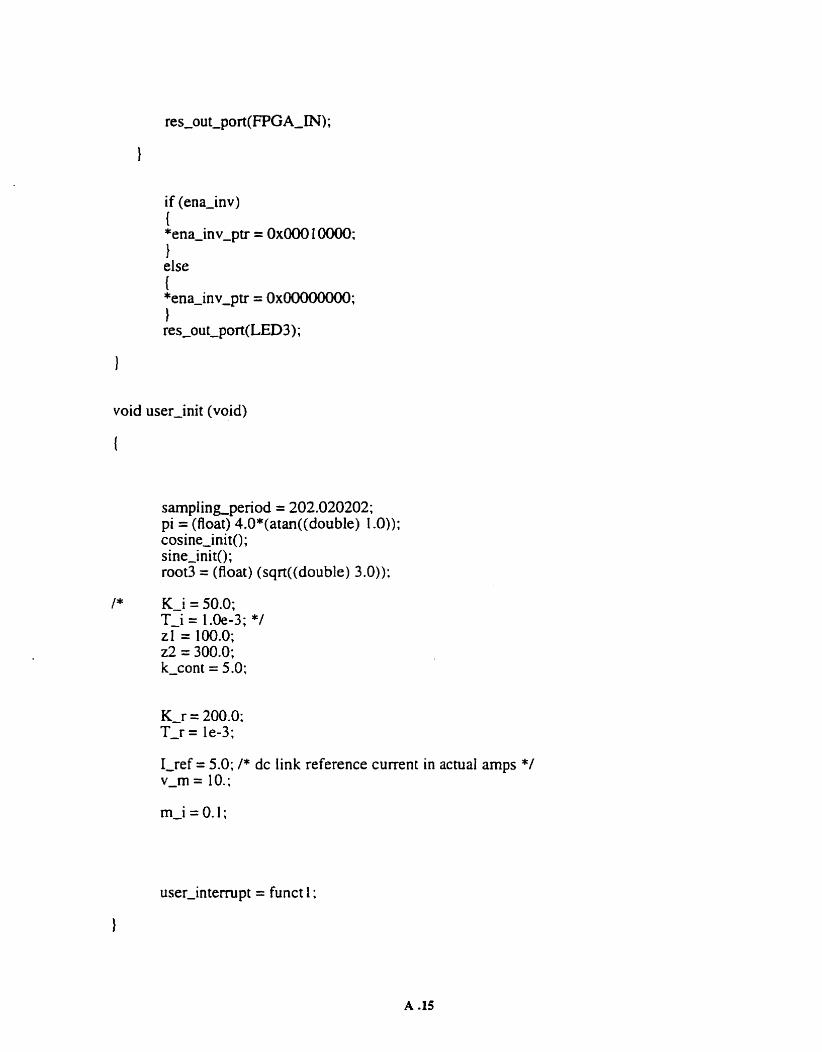
void user-init (void)
samplingperiod = 202.020202; pi = (float) 4.0*(atan((double) 1 .O)); cosine-init(); sine-init(); root3 = (float) (sqrt((doub1e) 3.0));
1-ref = 5.0; 1* dc link reference current in actual amps */ v-rn = 10.;
user-intempt = funct 1 ;

IMAGE NALUATION TEST TARGET (QA-3)
APPLIED A IMAGE . lnc a 1653 East Main Street - -. , - Rochester. NY 14609 USA -- --= Phone: 71 61482-0300 -- --II Fax: 71 6î288-5989
O 1993, Applied Image. Inc.. Ail Rights Reserved


