
IEEE Santa Clara Valley Chapter, Components, Packaging and Manufacturing Technology Society
February 21, 2013
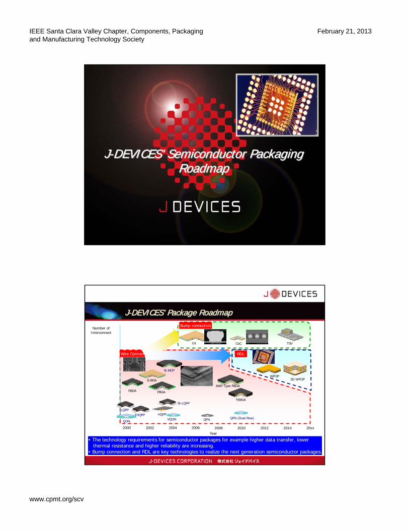
www.cpmt.org/scv
New Embedded Package Technology New Embedded Package Technology using Largeusing Large--Scale Panel AssemblyScale Panel Assembly((FOFO--WLP)WLP)
JJ--DEVICES CORPORATIONDEVICES CORPORATIONPackaging Research & Development CenterPackaging Research & Development Center
Akio KatsumataAkio Katsumata
About JAbout J--DEVICESDEVICES

IEEE Santa Clara Valley Chapter, Components, Packaging and Manufacturing Technology Society
February 21, 2013
www.cpmt.org/scv
About JAbout J--DEVICESDEVICES
Foundation・Established with capital from NAKAYA Micro Devices, Amkor and Toshibain 2009.・Merged Fujitsu Semiconductor’s assembly and test division (FIM) in 2012.・Will merge Renesas three assembly and test factories in 2013.
Goal・To become one of the leading global companies in the semiconductor backend business.
Focus・R&D is focused on developing new connecting technologies and has the experience to manufacture using new connecting technologies.
ex. Three years experience with 40um bump pitch CoC manufacturing.・Automotive product experience
Contents1. J-DEVICES’ Semiconductor Packaging Roadmap2. F0-WLP Market Trend & J-DEVICES’ Development
Concept3. WFOP Characteristics & Reliability4. Design Rule5. Target Applications & Roadmap6. Conclusion
ContentsContents
1. J1. J--DEVICESDEVICES’’ Semiconductor Packaging RoadmapSemiconductor Packaging Roadmap2. F02. F0--WLP Market Trend & JWLP Market Trend & J--DEVICESDEVICES’’ DevelopmentDevelopment
ConceptConcept3. WFOP Characteristics & Reliability3. WFOP Characteristics & Reliability4. Design Rule4. Design Rule5. Target Applications5. Target Applications & Roadmap& Roadmap6. Conclusion6. Conclusion
IEEE Santa Clara Valley Chapter, Components, Packaging and Manufacturing Technology Society
February 21, 2013
www.cpmt.org/scv
JJ--DEVICESDEVICES’’ Semiconductor PackagingSemiconductor PackagingRoadmap Roadmap
JJ--DEVICESDEVICES’’ Package RoadmapPackage Roadmap
St-MCP
VQONQONQFN (Dual Row)
HQFP
2000 2004 20102006Year
20082002 2012 2014
QFN
20xx
TEBGA
TSV
MAP Type PBGA
LQFP
PBGA
E-BGA
FBGA
St-LQFP
THQFP
CoCC4
Bump connection
Wire Connection RDL
WFOP3D WFOP
Number ofInterconnect
• The technology requirements for semiconductor packages for example higher data transfer, lowerthermal resistance and higher reliability are increasing.
• Bump connection and RDL are key technologies to realize the next generation semiconductor packages.

IEEE Santa Clara Valley Chapter, Components, Packaging and Manufacturing Technology Society
February 21, 2013
www.cpmt.org/scv
FOFO--WLP Market Trend & JWLP Market Trend & J--DEVICESDEVICES’’Development Concept Development Concept
Validity of FOValidity of FO--WLP TechnologyWLP Technology
Paradigm Paradigm ShiftShift
ONE by ONE Large panel assembly
Package design of FO-WLP is INDEPENDENT from chip size Fan-In WLPs are chip size package. All balls must fit UNDER chip shadow.
Large panel assembly Larger throughput
The pin unit price of a package falls drastically with enlargement of the panel size.
Design flexibility Redistribution layer easily forms 2D & 3D design.
Suitable for low package profile demand No need for wire bonding height and substrate thickness.

IEEE Santa Clara Valley Chapter, Components, Packaging and Manufacturing Technology Society
February 21, 2013
www.cpmt.org/scv
Market expectation of FOMarket expectation of FO--WLPWLPData Source : Data Source : YoleYole DevelopmentDevelopment
• The market is formed focusing on Mobile application and FO-WLP will be developed in Automotive and the Industrial market from 2014.
Data Source : Data Source : YoleYole DevelopmentDevelopmentMarket expectation of FOMarket expectation of FO--WLPWLP
• Firstly the markets is formed by Logic, RF, Power, Analog and Mixed signal devices.• Secondly the markets for Memory devices will be formed beginning 2015.

IEEE Santa Clara Valley Chapter, Components, Packaging and Manufacturing Technology Society
February 21, 2013
www.cpmt.org/scv
JJ--DEVICESDEVICES’’ FOFO--WLP Development Concept WLP Development Concept
Connect to Finer Pad Pitch50um Pad Pitch is achievable
Higher density RDLL/S=20/20(um) is achievable
Better thermal performancethan molded BGA
Better EMI Shielding effect
3D Packaging capability
Die stack structure is achievable
JJ--DEVICESDEVICES’’ WFOP TechnologyWFOP Technology
Backside view
Pad interconection SEM imageTop view of chip area
(Line width:20 um)
Resin
Metal Base Plate
Die Solder Ball
Redistribution layer
Adhesive
Package StructurePanel appearance
JJ--DEVICESDEVICES’’ AdvaAdvanntagetage
RDL is directly connected to the pad.
RDL technology is based on PCB technology which makes it cost-competitive.
Manufacturing work uses large panel.
50um pad pitch interconnection technology is already developed.

IEEE Santa Clara Valley Chapter, Components, Packaging and Manufacturing Technology Society
February 21, 2013
www.cpmt.org/scv
JJ--DEVICESDEVICES’’ WFOP TechnologyWFOP Technology
JJ--DEVICESDEVICES’’ WFOP TechnologyWFOP Technology
Pad interconection
Resin
Metal Plate
Die Solder Ball
Redistribution layerAdhesive
Metal Plate
Die
Redistribution layerAdhesive
Solder Ball Resin
Pad interconection1) Peripheral PAD interconnection
2) Area PAD interconnection • WFOP has two kinds of interconnection methods. (Lead-finger type and Via type)• The purpose of developing Lead-finger type is to realize finer connection to device pad.• The purpose of developing Via type is selection flexibility to insulator resin.

IEEE Santa Clara Valley Chapter, Components, Packaging and Manufacturing Technology Society
February 21, 2013
www.cpmt.org/scv
WFOPWFOP :: Redistribution layer Redistribution layer forfor 50um50um--pitch pitch padpads s
Lead-finger type connection
Seed layer formation (Ti/Cu)
Photo-resist coating for Copper wiring
Exposure and / Development
Copper plating
Resist removing
Seed layer etching
Insulating layer formation
Solder ball mounting
Singulation
Die attach to metal plate
Embedded dies by insulator resin
Via formation
Semi-additive process
Process Flow Process Flow

IEEE Santa Clara Valley Chapter, Components, Packaging and Manufacturing Technology Society
February 21, 2013
www.cpmt.org/scv
Comparison table of WFOP and Comparison table of WFOP and eWLBeWLB
WFOPTM eWLB
Package structure
RDL (Redistribution Line) formation technology
PCB semi-additive technologySemiconductor photolithography
Manufacturing work sizePanel (Large Size)
Wafer(200mmφ/300mmφ)
Minimum device pad pitch
50um
70umInfluence of die shift problem
caused by mold resin shrinkage
Resin
Metal Base Plate
Die Solder Ball
Redistribution layer
Adhesive
Cost competitive
Cost competitive
WFOP Characteristics & ReliabilityWFOP Characteristics & Reliability

IEEE Santa Clara Valley Chapter, Components, Packaging and Manufacturing Technology Society
February 21, 2013
www.cpmt.org/scv
⊿40%
⊿15%
⊿67%
⊿84%
FBGA > WFOP
FBGAWFOP
WFOP
FBGA
WFOP
FBGA
MotifBody size : 17mm□Ball counts : 529pinBase plate : Cu @WFOP
Thermal Characteristic of WFOPThermal Characteristic of WFOP
• The thermal resistance of WFOP is decreased because metal plateeffectively functions as a heat-spreader.
1mm
Probe
Sample
Amplifier
Network Analyzer
50Ω
Probe
sample
Magnetic field
Shield boxAmplifier
Measurement Condition
Samples & results
Package sample structure (No die, only Cu trace) Magnetic field strength
FBGA (Ref.) Reference
WFOP
WithoutGND metal plate
Reference -10dB
WithGND metal plate
Reference -30dB
Measurement results
* -10dB = 1/101, -30dB = 1/103
WFOP WFOP ::““EMI shieldingEMI shielding”” Effect of Metal Plate Effect of Metal Plate
• WFOP provides a better EMI shielding effect than FBGA.

IEEE Santa Clara Valley Chapter, Components, Packaging and Manufacturing Technology Society
February 21, 2013
www.cpmt.org/scv
WFOP
FBGA
Simulation results (Magnetic field)
Package size : 12 x 18mmDie size : 1.4 x 4.5mmFrequency : 1GHz
X-Z plane
Package
Package
-40dB
RDL
Power feeding
Bonding wire
Power feeding
WFOP WFOP ::““EMI shieldingEMI shielding”” Effect of Metal Plate Effect of Metal Plate
• The better shielding effect of WFOP is verified bysimulation.
-40
-20
0
20
40
60
80
-25 -15 -5 5 15 25X coordinate[mm]
Elec
tric
field
[dB]
WFOP
FBGA
Simulation results (Electric field)Package size : 12 x 18mmDie size : 1.4 x 4.5mmFrequency : 1GHz
X-Z plane
Package
Package
-76dB
RDL
Power feeding
Bonding wire
Power feeding
WFOP WFOP ::““EMI shieldingEMI shielding”” Effect of Metal Plate Effect of Metal Plate
• The better shielding effect of WFOP is verified bysimulation.

IEEE Santa Clara Valley Chapter, Components, Packaging and Manufacturing Technology Society
February 21, 2013
www.cpmt.org/scv
Warpage problem of current BGA PackageTh
erm
al e
xpan
sion
[ppm
]
HighLow
High
α1
α2
Low
TgTemp. [℃]
Cry
Smile
Open
Connection Failure
- Warpage direction is different because of environment temperature.- Shape of solder joint is affected by warpage.
→ To get higher solder joint reliability, it is necessary to reduce thewarpage caused by the environment temperature change.
The relationship between environment temperature and package warpage
Solder Joint Reliability Solder Joint Reliability
Advantage of WFOP
Deformed Shape at -25℃ (Corner Ball)
Warpage Variation on TCT Condition (125⇔-25℃)
1) The package warpage caused by the environment temperature changeis small because the metal plate has high elasticity.
2) C.T.E of the metal plate is adjustable to that of the mother board.
-4
-2
0
2
4
6
8
10
12
0 2 4 6 8 10 12
FBGA_125⇔-25℃
WFOP_125⇔-25℃
DNP [mm]
Pack
age
Dis
plac
emen
t [u
m]
MotifPackage size : 12x18Die size : 10x16mmSolder ball : 132pin
WFOP < FBGA
WFOP
FBGAWFOPFBGATemp.
125℃
-25℃
*Comparison with original shape
WFOP achieves improved solder joint reliabilityby optimizing the material property of metal plate.
Solder Joint Reliability Solder Joint Reliability

IEEE Santa Clara Valley Chapter, Components, Packaging and Manufacturing Technology Society
February 21, 2013
www.cpmt.org/scv
Z X
Y
WFOP
FBGA
Board
Base Plate
Board
Mold Resin
Die
Die
△εp maximum point
1.34%
2.14%
△εp maximum point
△εp : Equivalent plastic strain range
Solder Joint Reliability Solder Joint Reliability Strain Range Distribution Results using simulation(Temperature condition:-25℃125℃)
• Based on the difference of △εp, WFOP has a more than two times longer TCT life using Coffin-Manson equation.
Table1. Package Reliability
Items Result
TCT(MRT → -55ºC/125ºC)
> 1000 cycl.
PCT(MRT
→110ºC/1.2atm/85%)> 1000 hrs.
Items Result
THB mounted on PCB board(85°C/85%RH Vcc=3.6V) > 1000 hrs.
TCT mounted on PCB board(-25/125°C) > 2000 cycl.
PreconditionMRT: Soak:30ºC/70% x 216h
Reflow: 263ºC Max. x3
Table2. Board Level Reliability
6 mm SQ.
2 mm SQ.0.6mm (Chip size)
WFOP129-0606-0.40
0.4mm
(Pitch)
WFOP WFOP ::Package and Board level reliabilityPackage and Board level reliability
• WFOP provides sufficient “Package-level” and “Board-level” reliability.

IEEE Santa Clara Valley Chapter, Components, Packaging and Manufacturing Technology Society
February 21, 2013
www.cpmt.org/scv
Design RuleDesign Rule
MetalSiResin1
Resin2Cu LayerSolder resistBall
aa
d1d1
ffee
gg
bb
cc
PPII
d2d2
Parts Nominal(mm)
a Base Plate 0.300
b DAF 0.010
c Die 0.050
d1 Resin 1 0.070
d2 Resin 2 0.010
e Solder resit 0.010
f Cu layer 0.020
g Stand off 0.200
Pakcage height 0.600
CrossCross--section Design Rulesection Design Rule

IEEE Santa Clara Valley Chapter, Components, Packaging and Manufacturing Technology Society
February 21, 2013
www.cpmt.org/scv
Design Rule to connect Peripheral Pad Design Rule to connect Peripheral Pad
Current Design Rule Next generation
Die
Die pad
Pad opening (opening collectively)
L1 Copper patternL/S = 20um/ 20um
Via land [80um dia.](adjacent solder ball)
50um
50um pitch 45um pitch
Die
Die pad
Pad opening (opening collectively)
L1 Copper patternL/S 15um/ 15um*1
18um/ 18um*2
Via land [70um*1/ 65um*2 dia.](adjacent solder ball)
45um
*1:option-1 ,*2:option-2
Via (Interlayer connect) Ball land
EF
G
H
Pad connect(Area pad)
CD
I
K
J K’
Zoom
Die
Die pad
Pad opening (opening separately)
L1 Cu pattern
Via land (adjacent solder ball)
Symbol ItemDesign value
CurrentNext generation
Option-1 Option-2Line width 20um 15um 18umLine space 20um 15um 18um
C Die pad opening diameter 50um 40um 40umD Via land diameter 80um 70um 65umE Via land diameter 80um 70um 65umF Via diameter 50um 40um 40umG Via land -line space 20um 15um 18umH Via pitch 100um 85um 83umI Ball land diameter Refer other page J Ball land - line space 20um 15um 18umK Ball land – via land space
(Same NET) 0um
K’ Ball land – via land space (Different NET)
20um 15um 18um
Design Rule to connect Area Pad Design Rule to connect Area Pad

IEEE Santa Clara Valley Chapter, Components, Packaging and Manufacturing Technology Society
February 21, 2013
www.cpmt.org/scv
Target Applications & RoadmapTarget Applications & Roadmap
Application RF System LSI Memory
Replace Package
FBGA FC-BGA MCP
WFOP Structure
AdvantageEMI shielding effect
Better Electrical performanceReduce Thermal resistance
ThinnerBetter Electrical performance
Multi-ChannelReduce Thermal Resistance
JJ--DEVICESDEVICES’’ WFOP Package StructureWFOP Package Structure

IEEE Santa Clara Valley Chapter, Components, Packaging and Manufacturing Technology Society
February 21, 2013
www.cpmt.org/scv
• No need for bump and package substrate.• Like core-less substrate structure. Reduced capacitance and
inductance of wiring.
Material Thickness(Height)
Metal base plate 300um
Ball Stand-off(1mm pitch)
500um
Die 50um
Cu wiring 12um
Interlayer insulator 18um
RDL 2layers RDL 3layers
Package Total Height 935um 965um
Metal Base Plate Insulator-1
Solder BallRDL (Cu):
Single ~ Multi-layer
Die DAF
Solder Resist
Insulator-2
High Performance FCBGAHigh Performance FCBGA
WFOP FC-BGA
Base plate Die
RDL
Solder ball
Solder bump
Die
LID
Substrate
TIM
Solder ball
1mm
High Performance FCBGAHigh Performance FCBGA

IEEE Santa Clara Valley Chapter, Components, Packaging and Manufacturing Technology Society
February 21, 2013
www.cpmt.org/scv
MotifBody size : 35mm□Die size : 10mm□Ball counts : 900pinCu layers : 6Layers @FCBGA
3Layers @WFOPFCBGA TIM : 2.9W/MkWFOP DAF :15umMother board : JEDEC 4Layers
Thermal Characteristic of WFOPThermal Characteristic of WFOP
• WFOP (Copper) has the same heat resistance as FCBGA about ΘJA.• WFOP (Stainless) has similar heat resistance to FCBGA about θJC.
2013 2014 2015
Peripheral Pad Pitch
Routing layers
Minimum Line / Space
Noise guard
150 area
20/20 15/15
4layers
GND Lid
40 peripheral
Structure
Area Pad Connection PoP
Area Pad pitch 120 area
45um
Peripheral PAD Connection
High Performance FCBGA RoadmapHigh Performance FCBGA Roadmap

IEEE Santa Clara Valley Chapter, Components, Packaging and Manufacturing Technology Society
February 21, 2013
www.cpmt.org/scv
• Enables “Die stack module” without TSV structure.• Enables higher multi-channel memory module without custom memory devices.• Lower Thermal Resistance and high EMI shielding performance.
Material Thickness(Height)
Metal base plate 300um
Ball Stand-off(1.0mm pitch)
320um
Die 50um
Cu wiring 12um
Interlayer insulator 15um
RDL 3layers
Package Total Height 1055um
High Performance Flash Memory ModuleHigh Performance Flash Memory ModuleDie
2013 2014 2015
Min Line / Space
150um
40/40 20/20
Number of Dies
Number of Channels
4 dies /PKG 16 dies / PKG
Pad pitch 120um
8 dies / PKG
Total thickness 1.2mm / 4dies stack 1.0 mm / 8 dies stack1.2mm / 8 dies stack
Die thickness 50um 25um40um
4 Channels 16 Channels8 Channels
Structure
High Performance Flash Memory Module RoadmapHigh Performance Flash Memory Module Roadmap

IEEE Santa Clara Valley Chapter, Components, Packaging and Manufacturing Technology Society
February 21, 2013
www.cpmt.org/scv
Internal Reliability Test PlanInternal Reliability Test Plan
Item Condition
MSL (Pre-conditioning) Soak:30C/70%RH/192HReflow:260C, 4times
PCT (with Pre-conditioning) 110C/1.2atm/85%/500H
TCT (with Pre-conditioning) -55C/125C/1000cycles
HTS 150C/1000H
HAST (with Pre-conditioning) 110C/85%/3.6V/300H
THB 85C/85%RH/3.6V/1000H
Board level TCT TBD
Drop test TBD
Item Condition
MSL (Pre-conditioning) Soak:30C/70%RH/216HReflow:260C, 3times
PCT (with Pre-conditioning) 110C/1.2atm/85%/500H
TCT (with Pre-conditioning) -55C/125C/500cycles
HTS 150C/1000H
THB (with Pre-conditioning) Pre-conditioning 85C/85%RH/5.5V/1000H
FC-BGA Type.
Memory Type.
ConclusionConclusion
•The technology requirements for semiconductor packages for example higher datatransfer, lower thermal resistance and higher reliability are increasing.Bump connection and RDL are key technologies to realize next generation packages.
•Panel scale assembly is a new solution to change the packaging manufacture style. (from One by One to Batch Processing)
•The development concept of WFOP is connect to finer pad pitch, thermalperformance, EMI shielding and 3D packaging capability.
•Internal reliability test will be finished by end of April using the high performanceFCBGA and high performance flash memory module structure.

IEEE Santa Clara Valley Chapter, Components, Packaging and Manufacturing Technology Society
February 21, 2013
www.cpmt.org/scv


