Download - iCE40 UltraPlus Mobile Development Platform

iCE40 UltraPlus Mobile Development Platform
Evaluation Board User Guide
FPGA-EB-02007 Version 1.2
October 2018

iCE40 UltraPlus Mobile Development Platform Evaluation Board User Guide
© 2017-2018 Lattice Semiconductor Corp. All Lattice trademarks, registered trademarks, patents, and disclaimers are as listed at www.latticesemi.com/legal. All other brand or product names are trademarks or registered trademarks of their respective holders. The specifications and information herein are subject to change without notice.
2 FPGA-EB-02007-1.2
Contents 1. Introduction ................................................................................................................................................................. 4 2. Features ....................................................................................................................................................................... 5 3. Power and Battery ....................................................................................................................................................... 8
3.1. Power Source ...................................................................................................................................................... 8 3.2. Current Measurement Test Points ...................................................................................................................... 8 3.3. Battery Management and 4.2 V Regulator .......................................................................................................... 8
4. Clock Sources ............................................................................................................................................................... 9 5. Software Requirements ............................................................................................................................................. 10 6. Demonstrations ......................................................................................................................................................... 11
6.1. Mobile Display Demonstration on U1 ............................................................................................................... 11 6.2. Audio Microphone Demonstrations on U2 ....................................................................................................... 11 6.3. RGB LED Demonstration on U3 ......................................................................................................................... 11 6.4. Sensor Demonstrations on U3 .......................................................................................................................... 12 6.5. Face Recognition Demonstration on U4 ........................................................................................................... 12
7. Board Configuration and Programming ..................................................................................................................... 14 7.1. Jumpers and Switches ....................................................................................................................................... 14 7.2. Programming the iCE40 Devices Configuration Memory (CRAM) .................................................................... 17 7.3. Programming Onboard SPI Flash ....................................................................................................................... 18
8. Communication Channels .......................................................................................................................................... 20 8.1. USB .................................................................................................................................................................... 20 8.2. Bluetooth ........................................................................................................................................................... 20
9. Ordering Information ................................................................................................................................................. 20 10. PCB Revision History .................................................................................................................................................. 20 References .......................................................................................................................................................................... 21
Standards Documents ..................................................................................................................................................... 21 Lattice Semiconductor Documents ................................................................................................................................. 21
Technical Support Assistance ............................................................................................................................................. 21 Appendix A. iCE40 UltraPlus Mobile Development Board Schematics ............................................................................... 22 Appendix B. iCE40 UltraPlus Mobile Development Board Bill of Materials ........................................................................ 36
Accessories ..................................................................................................................................................................... 42 Revision History ................................................................................................................................................................... 43

iCE40 UltraPlus Mobile Development Platform Evaluation Board User Guide
© 2017-2018 Lattice Semiconductor Corp. All Lattice trademarks, registered trademarks, patents, and disclaimers are as listed at www.latticesemi.com/legal. All other brand or product names are trademarks or registered trademarks of their respective holders. The specifications and information herein are subject to change without notice.
FPGA-EB-02007-1.2 3
Figures Figure 2.1. iCE40 UltraPlus Mobile Development Platform Board (Top Side) ...................................................................... 6 Figure 2.2. iCE40 UltraPlus Mobile Development Platform Board (Bottom Side) ................................................................ 7 Figure 3.1. Power Block Diagram .......................................................................................................................................... 8 Figure 4.1. Clock Sources for the iCE40 UltraPlus MDP Board ............................................................................................. 9 Figure 6.1. Rework Resistor Positions Described in Parallel Video Bus Configuration ....................................................... 13 Figure 7.1. Board Configuration for Programming iCE40 UltraPlus Device “UI” ................................................................ 15 Figure 7.2. Programming iCE40 Devices on Board.............................................................................................................. 17 Figure 7.3. Programming SPI Flash on Board ...................................................................................................................... 18 Figure A.1. Block Diagram ................................................................................................................................................... 22 Figure A.2. iCE40UP5K FPGA A - Display ............................................................................................................................. 23 Figure A.3. iCE40UP5K FPGA B - Audio ............................................................................................................................... 24 Figure A.4. iCE40UP5K FPGA C - Sensor .............................................................................................................................. 25 Figure A.5. iCE40UP5K FPGA D - Camera ............................................................................................................................ 26 Figure A.6. Common Components- SPI ............................................................................................................................... 27 Figure A.7. Display Circuitry ................................................................................................................................................ 28 Figure A.8. Audio Circuitry .................................................................................................................................................. 29 Figure A.9. Sensor & RGB Circuitry ..................................................................................................................................... 30 Figure A.10. Camera Circuitry ............................................................................................................................................. 31 Figure A.11. USB Programming .......................................................................................................................................... 32 Figure A.12. Power Supplies ............................................................................................................................................... 33 Figure A.13. Common Components .................................................................................................................................... 34 Figure A.14. Battery Connector & Charger ......................................................................................................................... 35
Tables Table 7.1. iCE40 UltraPlus Device Selection ....................................................................................................................... 14 Table 7.2. iCE40 UltraPlus Device Selection Summary ....................................................................................................... 16

iCE40 UltraPlus Mobile Development Platform Evaluation Board User Guide
© 2017-2018 Lattice Semiconductor Corp. All Lattice trademarks, registered trademarks, patents, and disclaimers are as listed at www.latticesemi.com/legal. All other brand or product names are trademarks or registered trademarks of their respective holders. The specifications and information herein are subject to change without notice.
4 FPGA-EB-02007-1.2
1. Introduction Thank you for choosing the Lattice iCE40 UltraPlus™ Mobile Development Platform (MDP) Board.
This MDP board is an easy-to-use platform for demonstrating various features of the iCE40 UltraPlus for mobile applications. The MDP form-factor is similar to a mobile device (cell phone), with various sensors, display, Bluetooth communication, and others. The board contains four individual iCE40 UltraPlus devices, each configured with a unique set of interfaces to support multiple demonstrations.
Features that can be demonstrated using this board include:
Mobile Display (Onboard 1.54 inch 240 x 240 RGB wearable type display with MIPI DSI interface)
Camera (Onboard VGA 640 x 480 sensor with CSI and parallel video interface option)
Image and facial recognition
Microphones (Onboard Dual I2S and Dual PDM microphones with audio amp, 3.5 mm and expansion connectors)
Voice recognition
Audio beam forming capabilities
Sensors (Various Mobile Type Sensors with expansion connector)
RGB LED
Pressure Sensor
Compass Sensor
Gyroscope Sensor
Accelerometer Sensor
This guide describes how to begin using the MDP. The contents of this user guide include top-level functional descriptions of the various portions of the evaluation board, a summary of demonstrations, descriptions of the onboard connectors, switches, jumpers, configuration options, along with a complete set of schematics and the bill of materials.
Note: Static electricity can severely shorten the lifespan of electronic components. Be careful to follow proper ESD prevention handling standards when handling and using the iCE40 UltraPlus Mobile Development Platform Board.

iCE40 UltraPlus Mobile Development Platform Evaluation Board User Guide
© 2017-2018 Lattice Semiconductor Corp. All Lattice trademarks, registered trademarks, patents, and disclaimers are as listed at www.latticesemi.com/legal. All other brand or product names are trademarks or registered trademarks of their respective holders. The specifications and information herein are subject to change without notice.
FPGA-EB-02007-1.2 5
2. Features The iCE40 UltraPlus Mobile Development Platform development kit includes the items below.
iCE40 UltraPlus Mobile Development Platform– PCB, case, and integrated Li-ion battery featuring:
Four iCE40 UltraPlus devices (U1-U4 iCE40UP5K-UWG30) in 30-Ball WLCSP packages
Large capacity of onboard SPI Flash memory (U37 Micron M25P80 8Mb) to store the FPGA demo bitstream for all four iCE40 UltraPlus devices
Example of a PCB design using 0.40 mm Ball Pitch package
Control switches to select which of the four devices is active (only one device is active at a time)
Standard USB cable for device programming (Lattice part number HW-USBN-2A, HW-USBN-2B or equivalent)
RoHS-compliant packaging and process
Key Components
iCE40UP5K-UWG30 (4 pieces)
Power Regulation
Bluetooth module
MIPI LCD Mobile Display (1.54 inch 240 x 240 RGB LH154Q01)
Camera image sensor OVM7692 VGA 640 x 480 (CSI and parallel video interface option)
Microphones (Dual I2S and Dual PDM microphones with audio amp, connectors for 3.5 mm and expansion)
RGB LED
Sensors that include:
– Barometric pressure sensor
– Compass sensor
– 3D accelerometer and 3D gyroscope sensor
– Three-axis linear accelerometer sensor
Pre-loaded Demo – The kit includes a pre-loaded MIPI LCD Mobile Display demo.
USB Connector Cable – A mini-B USB port provides power, a programming interface and communication channel for a PC to communicate directly to iCE40 devices.
iCE40 UltraPlus Mobile Development Platform Evaluation Board User Guide
© 2017-2018 Lattice Semiconductor Corp. All Lattice trademarks, registered trademarks, patents, and disclaimers are as listed at www.latticesemi.com/legal. All other brand or product names are trademarks or registered trademarks of their respective holders. The specifications and information herein are subject to change without notice.
6 FPGA-EB-02007-1.2
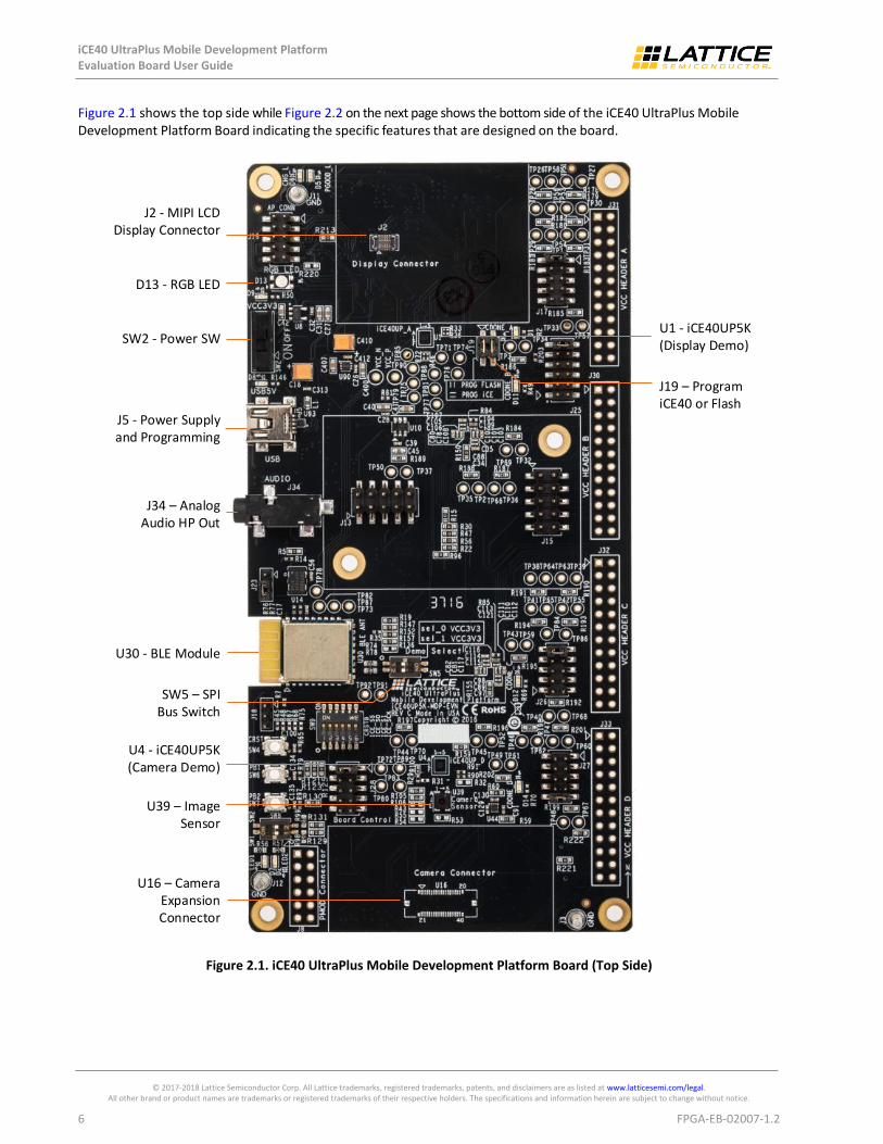
Figure 2.1 shows the top side while Figure 2.2 on the next page shows the bottom side of the iCE40 UltraPlus Mobile Development Platform Board indicating the specific features that are designed on the board.
J2 - MIPI LCDDisplay Connector
U1 - iCE40UP5K(Display Demo)
J19 – ProgramiCE40 or Flash
D13 - RGB LED
SW2 - Power SW
J5 - Power Supplyand Programming
J34 – AnalogAudio HP Out
U30 - BLE Module
SW5 – SPIBus Switch
U4 - iCE40UP5K(Camera Demo)
U39 – Image Sensor
U16 – CameraExpansion Connector
Figure 2.1. iCE40 UltraPlus Mobile Development Platform Board (Top Side)

iCE40 UltraPlus Mobile Development Platform Evaluation Board User Guide
© 2017-2018 Lattice Semiconductor Corp. All Lattice trademarks, registered trademarks, patents, and disclaimers are as listed at www.latticesemi.com/legal. All other brand or product names are trademarks or registered trademarks of their respective holders. The specifications and information herein are subject to change without notice.
FPGA-EB-02007-1.2 7
Battery
U94/19 – I2S
Microphones
U9 – FTDI
(USB to SPI)
U37 – SPI
Flash
U43 – Audio DAC
(I2S to Analog)
U2 – iCE40UP5K
(Audio Demo)
U95/12 – I2S
Microphones
U3 – iCE40UP5K
(Sensor Demo)
U35/22/36/38 –
Various Sensors
in Sensor Demo
Figure 2.2. iCE40 UltraPlus Mobile Development Platform Board (Bottom Side)

iCE40 UltraPlus Mobile Development Platform Evaluation Board User Guide
© 2017-2018 Lattice Semiconductor Corp. All Lattice trademarks, registered trademarks, patents, and disclaimers are as listed at www.latticesemi.com/legal. All other brand or product names are trademarks or registered trademarks of their respective holders. The specifications and information herein are subject to change without notice.
8 FPGA-EB-02007-1.2
3. Power and Battery
3.1. Power Source The MDP board can be powered by three sources:
External USB Connector J5 (5 V). Green LED D8 and Yellow LED D5 lights up when power is supplied.
External AP Header Connector J16-8 (5 V) and J16-9 (GND). Yellow LED D5 lights up when power is supplied.
Internal 250 mAH Li-ion battery contained internal to the MDP case.
External power from USB connector J5 and AP header connector J16 are 'Diode-ORd'. If power is supplied to both connectors, the higher voltage powers the board. When external power is not supplied, the internal Li-ion battery contained in the case powers the board.
Power switch SW2 turns the board ON and OFF by enabling/disabling the main voltage regulator outputs of 3.3 V, 2.5 V, and 1.2 V. Green LED D9 lights up when the 3.3 V rail is active and indicates that the board is powered ON.
USB
J16CONN
Li-ionBATT
BQ24232VSUPPLY 4.2 V
POWERSWITCH
VREG 3.3 V
VREG 2.5 V
VREG 1.2 V & 1.8 V
VREG 1.5 V & 2.8 V
VREG 1.8 V & 3.0 V
FLASH, BLE,GYRO, FGDI
VREG LEDBACKLIGHT
FPGAs VPP2V5
FPGAs VCC
FPGAs VCCIO
CAMERA SENSOROVM7692
DISPLAYDIODES 3.3 V
2.5 V
1.2 V
1.8 V
1.5 V
2.8 V
1.8 V
3.0 V
Figure 3.1. Power Block Diagram
3.2. Current Measurement Test Points Each of the four FPGAs have six 1 Ω resistors in series with their power inputs to allow easy current measurements using a voltmeter and to ease reworking VCCIO voltage rails. See Appendix A. iCE40 UltraPlus Mobile Development Board Schematics for details.
3.3. Battery Management and 4.2 V Regulator Chip BQ24232 U15 provides automatic battery management and the board's 4.2 V regulated voltage rail. The 4.2 V rail (VSUPPLY) is used to generate all of the board's other voltages. The management chip is always ON (not controlled by power switch SW2).
When external power is not available, the management chip uses the 250 mAH Li-ion battery internal to MDP case to generate the 4.2 V rail.
When external 5 V is supplied (4.6 V to 6.0 V), the battery is automatically charged as required. The Green LED D6 lights during charging and turns OFF when charging is complete. Additionally, external power is used to generate the 4.2 V rail. The BQ24232 battery charging is configured with external resistors.
Default resistor configuration:
500 mA input current limit
200 mA charging current
25 mA end of charging termination current threshold
5-hour fast charge time and 30-minute pre-charge

iCE40 UltraPlus Mobile Development Platform Evaluation Board User Guide
© 2017-2018 Lattice Semiconductor Corp. All Lattice trademarks, registered trademarks, patents, and disclaimers are as listed at www.latticesemi.com/legal. All other brand or product names are trademarks or registered trademarks of their respective holders. The specifications and information herein are subject to change without notice.
FPGA-EB-02007-1.2 9
4. Clock Sources A 27 MHz oscillator is built on the Mobile Development Platform board. External clock input can also be provided to this board depending on the J23 settings.
There are six devices sharing the same clock source that are available at the same time. These include four iCE40UP5K-UWG30 (U1~U4) devices that are responsible for various demos, U43 which is a stereo audio DAC with direct drive headphone amplifier, and U39 which is an ultra-compact size 640 x 480 image sensor.
Short Pins 2-3 leads the onboard 27 MHz clock to these devices and provides external clock source through Pin 2 and Pin 3 (GND).
U14
On Board
27 MHz
External
Clock
Source
U1 ICE40UP5K – A
(Display Demo)
U2 ICE40UP5K – B
(Audio Demo)
U3 ICE40UP5K – C
(Sensor Demo)
U4 ICE40UP5K – D
(Camera Demo)
U43 Max9850
(Audio DAC&Amplifier, Audio Demo)
U39 OVM7692
(Image Sensor, Camera Demo)
Figure 4.1. Clock Sources for the iCE40 UltraPlus MDP Board

iCE40 UltraPlus Mobile Development Platform Evaluation Board User Guide
© 2017-2018 Lattice Semiconductor Corp. All Lattice trademarks, registered trademarks, patents, and disclaimers are as listed at www.latticesemi.com/legal. All other brand or product names are trademarks or registered trademarks of their respective holders. The specifications and information herein are subject to change without notice.
10 FPGA-EB-02007-1.2
5. Software Requirements Install the following software before you begin developing designs for the board:
Lattice iCEcube2 2017.01 (or higher) Used for developing your own custom designs for the iCE40 UltraPlus FPGA.
Diamond Programmer® 3. 8 (or higher) Used to program the iCE40 UltraPlus FPGA.
These software programs are available at the www.latticesemi.com/software. Make sure you log in to www.latticesemi.com, otherwise these software downloads will not be visible.

iCE40 UltraPlus Mobile Development Platform Evaluation Board User Guide
© 2017-2018 Lattice Semiconductor Corp. All Lattice trademarks, registered trademarks, patents, and disclaimers are as listed at www.latticesemi.com/legal. All other brand or product names are trademarks or registered trademarks of their respective holders. The specifications and information herein are subject to change without notice.
FPGA-EB-02007-1.2 11
6. Demonstrations Four iCE40UP5K-UWG30 (U1-U4) devices are used on the Mobile Development Platform board. The devices are responsible for specific demonstrations. Lattice provides separate user guides that describe each demo in detail. The documents cover board configuration and step-by-step instructions. Please refer to the relevant documents for more details.
The following sections describe the Mobile Development Platform board demos.
6.1. Mobile Display Demonstration on U1 This demo showcases the ability of iCE40 UltraPlus to drive a small wearable display and buffer one full image frame.
Key components for this demo include:
U1 iCE40UP5K-UWG30
J2 Display connector for MIPI LCD display (MIPI LCD Display, 1.4” LH154Q01 is included in the kit.)
U11 Display backlight driver
U13 1.8 V and 3.0 V voltage regulator
Note: Be careful with the LCD display ribbon, it is fragile and can be damaged!
6.2. Audio Microphone Demonstrations on U2 FPGA U2 is optimized for microphone related demonstrations, such as audio beam. The board contains two I2S microphones, two PDM microphones, a 3.5 mm audio jack driven by a MAX9850 headphone audio amplifier, and an expansion connector allowing up to seven microphones used in an array. This demo shows the capability of picking up human voice and driving the output on the speaker with the same quality, irrespective of where the voice is originating from within a room.
Key components for this demo include:
U2 iCE40UP5K-UWG30
U12/U19 I2S omnidirectional microphone with Bottom Port and Analog Output
U94/U95 PDM omnidirectional microphone with Bottom Port and Analog Output
U43 Audio DAC with headphone amplifier.
J34 3.5 mm audio jack for analog output
J15 Expansion connector supporting up to seven microphones.
J25 Header used to configure FPGA to microphone connections
6.3. RGB LED Demonstration on U3 This demo showcases the capability of ICE40-UltraPlus to control and drive an RGB LED. A mobile app software GUI tool is provided to allow a user to remotely control the LED via a phone or tablet over Bluetooth. The features of the demo include:
Ability to control the color of the LED from a color palette.
Ability to control the brightness of the LED.
Ability to control the ON/OFF time of the LED – thereby creating a pulsating breathing effect.
Key components for this demo include:
U3 iCE40UP5K-UWG30
D13 RGB LED
U30 Bluetooth Module used for remote control

iCE40 UltraPlus Mobile Development Platform Evaluation Board User Guide
© 2017-2018 Lattice Semiconductor Corp. All Lattice trademarks, registered trademarks, patents, and disclaimers are as listed at www.latticesemi.com/legal. All other brand or product names are trademarks or registered trademarks of their respective holders. The specifications and information herein are subject to change without notice.
12 FPGA-EB-02007-1.2
It is recommended to download the RGB LED software GUI which interfaces with the MDP. This GUI allows you to control the RGB LED for color, brightness, blinking and ‘breathing’. Download the PC or MAC version of the GUI at www.latticesemi.com/ice40ultraplusmdp.
6.4. Sensor Demonstrations on U3 This demo showcases the capability of iCE40 UltraPlus to act as a sensor hub.
Key components for this demo include:
U3 iCE40UP5K-UWG30
U22 Digital barometric pressure sensor
U35 High performance e-compass 3D accelerometer and 3D magnetometer
U36 3D accelerometer and 3D gyroscope
U38 3-axis "pico" accelerometer
6.5. Face Recognition Demonstration on U4 This demo showcases the capability of ICE40-UltraPlus to detect and react to a general human face.
Key components for this demo include:
U4 iCE40UP5K-UWG30
U39 Image Sensor OVM7692
U16 Camera Expansion Connector
U44 1.5 V and 2.8 V voltage regulator
This demo uses the VGA (640 x 480) sensor OVM7692 U39 or the camera expansion connector U16. The default interface uses CSI2, however, the interface can be configured for 3.3 V parallel video interface to support the facial recognition demo with the following rework:
1. Remove resistors: R15, R29, R30, R47, R73, R90, R91, R100, R125, R126, R127, R142, R143, R149, R150, R154, R155.
2. Install 0 Ω resistors (or short with solder blob): R31, R32, R43, R52, R53, R54, R55, R56.
3. Verify resistors installed: R22, R159, R160.
4. If using Xtal U14 as clock source Jumper J23-2 and 3 else J23-2 should be open.

iCE40 UltraPlus Mobile Development Platform Evaluation Board User Guide
© 2017-2018 Lattice Semiconductor Corp. All Lattice trademarks, registered trademarks, patents, and disclaimers are as listed at www.latticesemi.com/legal. All other brand or product names are trademarks or registered trademarks of their respective holders. The specifications and information herein are subject to change without notice.
FPGA-EB-02007-1.2 13
Figure 6.1 shows the resistors of the rework. Resistors highlighted in red rectangle need to be removed; resistors highlighted in green rectangle need to install 0 Ω resistors; blue highlights show the resistors needing installation verification.
J23
U14 Xtal
U4 iCE40
U39 OVM7692
U16
Camera
Connector
J33
R142
U37
Flash
Figure 6.1. Rework Resistor Positions Described in Parallel Video Bus Configuration
iCE40 UltraPlus Mobile Development Platform Evaluation Board User Guide
© 2017-2018 Lattice Semiconductor Corp. All Lattice trademarks, registered trademarks, patents, and disclaimers are as listed at www.latticesemi.com/legal. All other brand or product names are trademarks or registered trademarks of their respective holders. The specifications and information herein are subject to change without notice.
14 FPGA-EB-02007-1.2
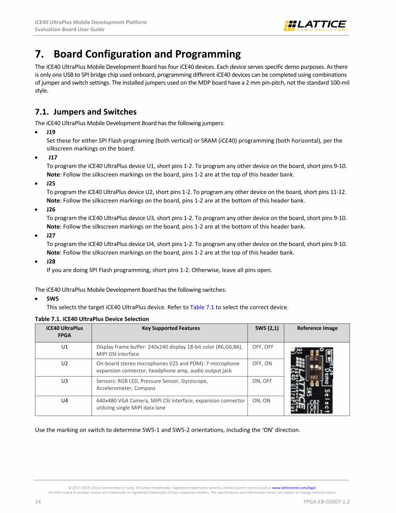
7. Board Configuration and Programming The iCE40 UltraPlus Mobile Development Board has four iCE40 devices. Each device serves specific demo purposes. As there is only one USB to SPI bridge chip used onboard, programming different iCE40 devices can be completed using combinations of jumper and switch settings. The installed jumpers used on the MDP board have a 2 mm pin-pitch, not the standard 100-mil style.
7.1. Jumpers and Switches The iCE40 UltraPlus Mobile Development Board has the following jumpers:
J19
Set these for either SPI Flash programing (both vertical) or SRAM (iCE40) programming (both horizontal), per the silkscreen markings on the board.
J17
To program the iCE40 UltraPlus device U1, short pins 1-2. To program any other device on the board, short pins 9-10.
Note: Follow the silkscreen markings on the board, pins 1-2 are at the top of this header bank.
J25
To program the iCE40 UltraPlus device U2, short pins 1-2. To program any other device on the board, short pins 11-12.
Note: Follow the silkscreen markings on the board, pins 1-2 are at the bottom of this header bank.
J26
To program the iCE40 UltraPlus device U3, short pins 1-2. To program any other device on the board, short pins 9-10.
Note: Follow the silkscreen markings on the board, pins 1-2 are at the bottom of this header bank.
J27
To program the iCE40 UltraPlus device U4, short pins 1-2. To program any other device on the board, short pins 9-10.
Note: Follow the silkscreen markings on the board, pins 1-2 are at the top of this header bank.
J28
If you are doing SPI Flash programming, short pins 1-2. Otherwise, leave all pins open.
The iCE40 UltraPlus Mobile Development Board has the following switches:
SW5
This selects the target iCE40 UltraPlus device. Refer to Table 7.1 to select the correct device.
Table 7.1. iCE40 UltraPlus Device Selection
iCE40 UltraPlus FPGA
Key Supported Features SW5 (2,1) Reference Image
U1 Display frame buffer: 240x240 display 18-bit color (R6,G6,B6), MIPI DSI interface
OFF, OFF
U2 On-board stereo microphones (I2S and PDM): 7-microphone expansion connector, headphone amp, audio output jack
OFF, ON
U3 Sensors: RGB LED, Pressure Sensor, Gyroscope, Accelerometer, Compass
ON, OFF
U4 640x480 VGA Camera, MIPI CSI interface, expansion connector utilizing single MIPI data lane
ON, ON
Use the marking on switch to determine SW5-1 and SW5-2 orientations, including the ‘ON’ direction.
iCE40 UltraPlus Mobile Development Platform Evaluation Board User Guide
© 2017-2018 Lattice Semiconductor Corp. All Lattice trademarks, registered trademarks, patents, and disclaimers are as listed at www.latticesemi.com/legal. All other brand or product names are trademarks or registered trademarks of their respective holders. The specifications and information herein are subject to change without notice.
FPGA-EB-02007-1.2 15
SW9
This switch is used to add/remove the BLE module from the SPI bus. It is recommended that the BLE module be removed from the SPI bus when the module is not in demo use.
Figure 7.1 shows the setting of jumpers and switches while trying to program iCE40 device “U1”directly.
J17 – Short pins 1-2programming iCE40 device UI
SW2 – Slide on to power on board
J5 – Power Supplyand Programming
J25 – Short pins 11-12
J17 – Short pins 1-2programming iCE40 device UI
J19 – Put jumpers horizontal to directlyprogram iCE40 device
J26 – Short pins 9-10
J27 – Short pins 9-10
J28 – Short pins 1-2 to program SPI Flash
SW9 – Set all pins in SW9 to OFF to remove
BLE from SPI Bus
SW5 – Set 2 pins both to OFF to select iCE40
device “UI”
Figure 7.1. Board Configuration for Programming iCE40 UltraPlus Device “UI”

iCE40 UltraPlus Mobile Development Platform Evaluation Board User Guide
© 2017-2018 Lattice Semiconductor Corp. All Lattice trademarks, registered trademarks, patents, and disclaimers are as listed at www.latticesemi.com/legal. All other brand or product names are trademarks or registered trademarks of their respective holders. The specifications and information herein are subject to change without notice.
16 FPGA-EB-02007-1.2
Table 7.2. iCE40 UltraPlus Device Selection Summary
SPI Flash Demux
CRESET Boot Control Jumper Placement
Section iCE40 UltraPlus
RefDes SW5 (2,1) J17 J25 J26 J27
Camera U1 OFF,OFF 1-2 11-12 9-10 9-10
Audio U2 OFF, ON 9-10 1-2 9-10 9-10
Sensor/RGB U3 ON, OFF 9-10 11-12 1-2 9-10
Display U4 ON, ON 9-10 11-12 9-10 1-2
iCE40 UltraPlus Mobile Development Platform Evaluation Board User Guide
© 2017-2018 Lattice Semiconductor Corp. All Lattice trademarks, registered trademarks, patents, and disclaimers are as listed at www.latticesemi.com/legal. All other brand or product names are trademarks or registered trademarks of their respective holders. The specifications and information herein are subject to change without notice.
FPGA-EB-02007-1.2 17
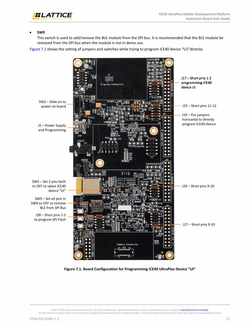
7.2. Programming the iCE40 Devices Configuration Memory (CRAM) To program iCE40 UltraPlus devices’ CRAM in Diamond Programmer:
1. Set board jumpers on J19 horizontally for CRAM programming.
2. Remove board jumper J28: 1-2 for CRAM programming.
3. Use Diamond Programmer 3.8 or later.
4. Connect the iCE40 UltraPlus Mobile Development Platform board via the USB cable to a PC or MAC.
5. Start Diamond Programmer.
6. Set Device Family to iCE40 UltraPlus” and Device to “iCE40UP5K”. Refer Figure 7.2 below.
7. Be sure to perform the “Program, Verify” operation. If you select only the “Program” operation, you may get a false positive that the device has programmed.
8. Field Programming Speed Settings should be set to “Use customer Clock Divider” and appropriate value “5” should be set in the text box below.
9. Open the Device Properties dialog. Apply the settings highlighted.
10. Access mode: set to “CRAM programming” to allow directly programming iCE40 devices.
11. Operation: set to “Fast Program” mode.
12. Programming File: load bit stream file for demo.
13. Click OK to exit Device Properties dialog.
14. Click the Program button in Diamond Programmer to download the bit stream file.
Figure 7.2. Programming iCE40 Devices on Board

iCE40 UltraPlus Mobile Development Platform Evaluation Board User Guide
© 2017-2018 Lattice Semiconductor Corp. All Lattice trademarks, registered trademarks, patents, and disclaimers are as listed at www.latticesemi.com/legal. All other brand or product names are trademarks or registered trademarks of their respective holders. The specifications and information herein are subject to change without notice.
18 FPGA-EB-02007-1.2
7.3. Programming Onboard SPI Flash To program SPI flash in Diamond Programmer:
1. Set board jumpers on J19 vertically for SPI Flash programming.
2. Install board jumper J28: 1-2 for SPI Flash programming.
3. Start Diamond Programmer.
4. Set Device Family to iCE40 UltraPlus” and Device to “iCE40UP5K”.
5. Be sure to do the “Program, Verify” operation. If you select only the “Program” operation, you may get a false positive that the device has programmed.
6. Field Programming Speed Settings should be set to “Use customer Clock Divider” and appropriate value “5” should be set in the text box below.
7. Open the Device Properties dialog. Apply the settings highlighted.
Access mode: set to “SPI Flash Programming”.
Operation: set to “SPI Flash Erase, Program, Verify” mode.
Programming File: load bit stream file for demo.
SPI Flash Options: select correct Flash chip as shown in Figure 7.3 blow.
Load from File button should be used to refresh fields such as “Data file size” and “End address(Hex)”.
8. Click OK to exit Device Properties dialog.
9. Click the Program button in Diamond Programmer to download the bit stream file.
Figure 7.3. Programming SPI Flash on Board

iCE40 UltraPlus Mobile Development Platform Evaluation Board User Guide
© 2017-2018 Lattice Semiconductor Corp. All Lattice trademarks, registered trademarks, patents, and disclaimers are as listed at www.latticesemi.com/legal. All other brand or product names are trademarks or registered trademarks of their respective holders. The specifications and information herein are subject to change without notice.
FPGA-EB-02007-1.2 19
The main differences between programming ICE40 UltraPlus devices and programming SPI Flash are:
1. Board jumpers on J19: Vertical for CRAM programming and horizontal for SPI Flash programming.
2. Board jumpers J28: 1-2: Remove for CRAM programming and install for SPI Flash programming.
3. The settings in the Device Properties dialog box in Diamond Programmer.
For more information on Diamond Programmer, please refer to its user guide.

iCE40 UltraPlus Mobile Development Platform Evaluation Board User Guide
© 2017-2018 Lattice Semiconductor Corp. All Lattice trademarks, registered trademarks, patents, and disclaimers are as listed at www.latticesemi.com/legal. All other brand or product names are trademarks or registered trademarks of their respective holders. The specifications and information herein are subject to change without notice.
20 FPGA-EB-02007-1.2
8. Communication Channels To enable communication with external tools, devices or Apps on Smart phone, this board features a number of communication channels.
8.1. USB A USB cable from PC needs to be connected to J5 on board. This communication channel through U9 (FT2232H) is mainly used for programing the SPI flash on board, or program the ICE devices directly depends on settings on jumper J19.
8.2. Bluetooth This board features a Bluetooth module U30 to enable wireless communication with external devices like smart phones, which is very useful while need to run some APPs on smart phone in demos. This Bluetooth provide UART channel to communicate with ICE40 devices on board.
The operating range of the BLE module is up to 100 meters.
9. Ordering Information Description Ordering Part Number China RoHS Environment- Friendly Use Period (EFUP)
iCE40 UltraPlus Mobile Development Platform iCE40UP5K-MDP-EVN
10. PCB Revision History PCB Revision Notes
Rev A, Rev B Prototype revisions, unreleased
Rev C Production revision
Includes two wires added during assembly to connect the UART of the FT2232HL to test points. Specifically, these are U9-38 to J33-1 and U9-39 to J33-3.
Rev D Production revision
Implements the wires from Rev C as PCB traces.
Rev C and Rev D schematics are identical.

iCE40 UltraPlus Mobile Development Platform Evaluation Board User Guide
© 2017-2018 Lattice Semiconductor Corp. All Lattice trademarks, registered trademarks, patents, and disclaimers are as listed at www.latticesemi.com/legal. All other brand or product names are trademarks or registered trademarks of their respective holders. The specifications and information herein are subject to change without notice.
FPGA-EB-02007-1.2 21
References Standards Documents The standards used in this document and their abbreviations are listed on the table below.
Abbreviation Standards Publication, Organization, and Date
MIPI MIPI Alliance, Mobile Industry Processor Interface
CSI2 MIPI Alliance, Camera Serial Interface
For more information on the specifications that are applied in this document, contact the responsible standards groups listed on the table below.
Standards Group Web URL
MIPI Alliance http://www.mipi.org
Lattice Semiconductor Documents Related documents available from your Lattice Semiconductor sales representative are listed on the table below.
Document Title
Data Sheet DS1056 iCE40 UltraPlus Family Data Sheet
Technical Support Assistance Submit a technical support case through www.latticesemi.com/techsupport.

iCE40 UltraPlus Mobile Development Platform Evaluation Board User Guide
© 2017-2018 Lattice Semiconductor Corp. All Lattice trademarks, registered trademarks, patents, and disclaimers are as listed at www.latticesemi.com/legal. All other brand or product names are trademarks or registered trademarks of their respective holders. The specifications and information herein are subject to change without notice.
22 FPGA-EB-02007-1.2
Appendix A. iCE40 UltraPlus Mobile Development Board Schematics
Figure A.1. Block Diagram
5
5
4
4
3
3
2
2
1
1
D D
C C
B B
A A
LATTICE SEMICONDUCTOR CORPORATION CONFIDENTIAL
Revision History
Rev A - First Draft
iCE40 UltraPlus Mobile Development PlatformRevisi on DJune 27 2017
iCE40 UltraPlus Mobile Development Platform
iCE40UP5K_A: Display FPGASheet 2
iCE40UP5K_B: Audio FPGASheet 3
iCE40UP5K_C: Sensor / RGB FPGASheet 4
iCE40UP5K_D: Camera FPGASheet 5
DisplaySheet 7
MicrophonesAmplifierSheet 8
SensorsRGBSheet 9
CameraSheet 10
SPIMUXSheet 6
FTDISheet 11
AP ConnSheet 6
SPIFlashSheet 6
SwitchesSheet 6
BLEModuleSheet 6
CommonComponentsSheet 13
BatterySheet 14
Power SuppliesSheet 12
All pages
Rev C - Changed Gryroscope i2c address by grounding U36-27
- Inserted 2 more pins to iCEA control J25 header, pin 7 & 8
- Added 4 resistors to allow swap of GLED & BLED on U3 device
- Added FT_RESETb on J16.7 - AP INTERCONNECT to allow bypassing of FTDI Chip
- Added 2 PDM Microphones
- Added ESD protection for J5 USB
- Changed D2 - LED2 to GREEN from RED
- Changed R42 resistor value to 18ohm from 12ohm
- Changed U41 and U42 to DG409LDQ-T1-E3 device
- Changed U41 and U42 power to VSUPPLY
Title
Size Document Number Rev
Date: Sheet of
D
Block Diagram / Cover Page
B
1 14Thursday, November 02, 2017
Title
Size Document Number Rev
Date: Sheet of
D
Block Diagram / Cover Page
B
1 14Thursday, November 02, 2017
Title
Size Document Number Rev
Date: Sheet of
D
Block Diagram / Cover Page
B
1 14Thursday, November 02, 2017

iCE40 UltraPlus Mobile Development Platform Evaluation Board User Guide
© 2017-2018 Lattice Semiconductor Corp. All Lattice trademarks, registered trademarks, patents, and disclaimers are as listed at www.latticesemi.com/legal. All other brand or product names are trademarks or registered trademarks of their respective holders. The specifications and information herein are subject to change without notice.
FPGA-EB-02007-1.2 23
Figure A.2. iCE40UP5K FPGA A - Display
5
5
4
4
3
3
2
2
1
1
D D
C C
B B
A A
LATTICE SEMICONDUCTOR CORPORATION CONFIDENTIAL
iCE40 UltraPlus Mobile Development Platform
VCC Sense Resistors - 1 Ohm 0603Add test points on both sides
Note: Place close to DUT
Note: Place close to DUT
DONE_A
Function Mapping from iCE40UP to Board
Note: Place close to DUT
Note: Place close to DUT
Note: Place close to DUT To Interconnects Page
0201
To Display Connect Page
Place close to ICE40
Note :1) Match length within pair as well as other pairs with +/- 5% tolerence2)Differential impedance should be 100 Ohms and 50 Ohms as a single ended signals3)All the power rails should be capable of carrying 1A current4)Place MIPI TX resistor network as close to bank 1 as possible.Trace match *HS* P & N channels as well as individual pairs.Minimize routing and trace match *LP* signals..
VCC1V2
VCC2V5
VCC3V3
VCC3V3
VCC1V2
VCC_iCE_A
VCCPLL_IN_A
VPP2V5_A
VCCIO0_iCE_A
SPIVCCIO1_iCE_A
VCCIO2_iCE_A
VCC_iCE_A
VPP2V5_A
VCCPLL_IN_A
SPIVCCIO1_iCE_A
VCCIO2_iCE_A
SPIVCCIO1_iCE_A
VCCIO0_iCE_A
VCC3V3
iCE_SS_A{6}
CDONE{3,4,5,6,11}
iCE_SCK_A{6}iCE_SI_A{6}iCE_SO_A{6}
DSI_D0N {7}
DSI_CLKP {7}
DSI_CLKN {7}
DSI_D0P {7}
SPARE_A1 {7,13}
SPARE_A2 {7,13}
SPARE_A0 {7,13}
OSC_CLK {3,4,5,8,10,13}
UART_TX {3,4,5,6,10,13}UART_RX {3,4,5,6,10,13}
proc_cs {3,4,5,6,10}proc_intr {3,4,5,6,10}
CRSTb {3,4,5,6,10,11,13}I2S_SD_mic7 {3,8}
Title
Size Document Number Rev
Date: Sheet of
D
iCE40UP5K FPGA A - Display
B
2 14Friday, November 03, 2017
Title
Size Document Number Rev
Date: Sheet of
D
iCE40UP5K FPGA A - Display
B
2 14Friday, November 03, 2017
Title
Size Document Number Rev
Date: Sheet of
D
iCE40UP5K FPGA A - Display
B
2 14Friday, November 03, 2017
C130.1u
C31u
30R36 R0201
5%
R178 1
C80.1u
R22k2
R19 0
C50.1u
TP31
1KR38
5%R0201
J17
iCEA Control
246810
13579
R15 0
C100.1u
D1GREEN
21
R180 1
30R72 R0201
5%
30R33 R0201
5%
R142 0 DNI
TP1J31
CON24A
1 23 45 67 89 10
11 1213 1415 1617 1819 2021 2223 24
R1100
C20.1u
R141 0
R143 0 DNI
C910n
C141u
R182 1
1KR71
5%R0201
TP26TP52
TP29TP28TP27
TP2
R179 1
Bank2
Bank1
Bank0
iCEUP5K-WLCSP30
iCE40UP5K-UWG30
U1
IOB_0AE5
IOB_2AD5
IOB_3B_G6F5
IOB_9BE4
IOB_10AC3
IOB_11B_G5F4
CRESET_BF3
IOB_12A_G4_CDONED3
IOB_13BE3
IOB_24AB1
IOB_25B_G3F2
IOB_32A_SPI_SOF1IOB_33B_SPI_SIE1IOB_34A_SPI_SCKD1IOB_35B_SPI_SSC1
VCCPLLB2
IOT_36BA1 IOT_37AA2
IOT_46B_G0B3
IOT_47AA4
RGB2A5
RGB1B5
RGB0C5
GN
DB
4
GN
DE
2
VCCC2
VCCIO_0A3
SPI_VCCIO1D2
VCCIO_2C4
VPP_2V5D4
C710u
1KR34
5%R0201
TP3
30R46 R0201
5%
C1210n
C610n
1KR39
5%R0201
TP50
C110n
TP30
C111u
R183 1
R181 1
C41u
TP51
VCCPLL_ACDONE_A
CDONE
iCE_SS_AiCE_SCK_AiCE_SI_AiCE_SO_A
VCCPLL_A iCE_SS_AiCE_SCK_AiCE_SI_AiCE_SO_A
UART_TX_AUART_RX_A
OSC_CLK_A
CDONE_A
CRSTb_A
proc_cs_A
SPARE_A0SPARE_A1SPARE_A2
DSI_HS_CLKPDSI_HS_D0P
proc_intr_A
DSI_HS_D0N
DSI_HS_CLKN
DSI_LP_CLKPDSI_LP_CLKNDSI_LP_D0PDSI_LP_D0N
DSI_HS_D0P
DSI_HS_D0N
DSI_HS_CLKP
DSI_HS_CLKN
DSI_D0P
DSI_CLKN
DSI_LP_D0P
DSI_LP_D0N
DSI_LP_CLKP
DSI_LP_CLKN
DSI_D0N
DSI_CLKP
SPARE_A0
SPARE_A1
SPARE_A2
OSC_CLK_A
UART_TX_AUART_RX_A
proc_cs_Aproc_intr_A
UART_TX_AUART_RX_A
OSC_CLK_Aproc_cs_A
iCE_SS_AiCE_SCK_AiCE_SI_AiCE_SO_ACRSTb_A
SPARE_A0SPARE_A1SPARE_A2
proc_intr_A
CDONECDONE_ACRSTb_A
CRSTb_ASPARE_A2

iCE40 UltraPlus Mobile Development Platform Evaluation Board User Guide
© 2017-2018 Lattice Semiconductor Corp. All Lattice trademarks, registered trademarks, patents, and disclaimers are as listed at www.latticesemi.com/legal. All other brand or product names are trademarks or registered trademarks of their respective holders. The specifications and information herein are subject to change without notice.
24 FPGA-EB-02007-1.2
Figure A.3. iCE40UP5K FPGA B - Audio
5
5
4
4
3
3
2
2
1
1
D D
C C
B B
A A
LATTICE SEMICONDUCTOR CORPORATION CONFIDENTIAL
Note: Place close to DUT
iCE40 UltraPlus Mobile Development Platform
DONE_B
Note: Place close to DUT
Note: Place close to DUT
Note: Place close to DUT
Note: Place close to DUT
VCC Sense Resistors - 1 Ohm 0603Add test points on both sides
SPIVCCIO1_iCE_B
SPIVCCIO1_iCE_BVCC_iCE_B
VPP2V5_B
VCCIO2_iCE_B
VCCIO0_iCE_B
VCCPLL_IN_B
VCC3V3
VCC2V5
VCC1V2
VCC3V3
VCC_iCE_B
VCCPLL_IN_B
VPP2V5_B
VCCIO0_iCE_B
SPIVCCIO1_iCE_B
VCCIO2_iCE_B
VCC3V3
VCC3V3
I2S_SCK_mic {8}I2S_WS_mic {8}
I2S_SD_mic3_mic4 {8}
I2C_amp_sda {8}
I2S_SD_mic1_mic2_onboard {8}
CDONE{2,4,5,6,11}
I2S_WS_amp {8}I2S_SCK_amp {8}I2S_SD_amp {8}
iCE_SI_B{6}iCE_SO_B{6}
iCE_SS_B{6}iCE_SCK_B{6}
I2C_amp_scl {8}
I2S_SD_mic1_mic2_card {8}
I2S_SD_mic5_mic6 {8}I2S_SD_mic7 {2,8}
OSC_CLK {2,4,5,8,10,13}
UART_TX {2,4,5,6,10,13}UART_RX {2,4,5,6,10,13}
proc_cs {2,4,5,6,10}proc_intr {2,4,5,6,10}
CRSTb {2,4,5,6,10,11,13}
PDM_SD_mic1_mic2_onboard{8}
Title
Size Document Number Rev
Date: Sheet of
D
iCE40UP5K FPGA B - Audio
B
3 14Friday, November 03, 2017
Title
Size Document Number Rev
Date: Sheet of
D
iCE40UP5K FPGA B - Audio
B
3 14Friday, November 03, 2017
Title
Size Document Number Rev
Date: Sheet of
D
iCE40UP5K FPGA B - Audio
B
3 14Friday, November 03, 2017
C10210n
D11GREEN
21
C1090.1u
R185 1
TP53
TP55
TP33
C1050.1u
R147 0
TP36
J25iCEA Control
13579
246810
11 12
R148 0
R169 0
J30
CON24A
DNL
1 23 45 67 89 10
11 1213 1415 1617 1819 2021 2223 24
R150 0 DNI
C351u
C780.1u
C1071u
R84100
TP57TP32
C10810n
Bank2
Bank1
Bank0
iCEUP5K-WLCSP30
iCE40UP5K-UWG30
U2
IOB_0AE5
IOB_2AD5
IOB_3B_G6F5
IOB_9BE4
IOB_10AC3
IOB_11B_G5F4
CRESET_BF3
IOB_12A_G4_CDONED3
IOB_13BE3
IOB_24AB1
IOB_25B_G3F2
IOB_32A_SPI_SOF1IOB_33B_SPI_SIE1IOB_34A_SPI_SCKD1IOB_35B_SPI_SSC1
VCCPLLB2
IOT_36BA1 IOT_37AA2
IOT_46B_G0B3
IOT_47AA4
RGB2A5
RGB1B5
RGB0C5
GN
DB
4
GN
DE
2
VCCC2
VCCIO_0A3
SPI_VCCIO1D2
VCCIO_2C4
VPP_2V5D4
R188 1
TP34
C1031u
R186 1
R149 0 DNI
C1010.1u
R184 1
TP37
TP56
C10610n
TP58
TP54
C10410u
R203100k
R170 0
R168 0
TP35
C340.1u
C8810n
R492k2
R189 1
C801u
R300
R187 1
I2S_SCK_micI2S_WS_mic
CDONE
I2S_WS_amp
VCCPLL_B
iCE_SS_BiCE_SCK_B
iCE_SI_BiCE_SO_B
UART_TX_BUART_RX_B
OSC_CLK_B
CDONE_B
CRSTb_B
proc_cs_B
I2S_SD_mic3_mic4I2S_SD_mic5_mic6I2S_SD_mic7
I2S_SCK_micI2S_SD_mic1_mic2
proc_intr_B
I2S_WS_amp
I2S_WS_mic
I2C_amp_sdaI2C_amp_sclI2S_SCK_ampI2S_SD_amp
I2S_SCK_amp
I2C_amp_sda
I2S_SD_mic3_mic4
CDONE_B
I2S_SD_amp
I2S_SD_mic1_mic2_onboardiCE_SS_BiCE_SCK_BiCE_SI_BiCE_SO_B
I2C_amp_scl
I2S_SD_mic1_mic2_card
I2S_SD_mic5_mic6I2S_SD_mic7
OSC_CLK_B
VCCPLL_B
UART_TX_BUART_RX_B
OSC_CLK_Bproc_cs_BI2S_WS_ampI2S_SCK_ampI2S_SD_ampI2C_amp_sdaI2C_amp_sclI2S_SD_mic5_mic6I2S_SD_mic7
iCE_SS_BiCE_SCK_BiCE_SI_BiCE_SO_BCRSTb_BI2S_SCK_micI2S_SD_mic1_mic2I2S_SD_mic3_mic4proc_intr_BI2S_WS_mic
UART_TX_BUART_RX_B
proc_cs_Bproc_intr_B
CRSTb_BI2S_SD_mic1_mic2_onboardI2S_SD_mic1_mic2_card I2S_SD_mic1_mic2
I2S_SD_mic1_mic2
CDONE_B CDONECRSTb_B
I2S_SD_mic1_mic2PDM_SD_mic1_mic2_onboard

iCE40 UltraPlus Mobile Development Platform Evaluation Board User Guide
© 2017-2018 Lattice Semiconductor Corp. All Lattice trademarks, registered trademarks, patents, and disclaimers are as listed at www.latticesemi.com/legal. All other brand or product names are trademarks or registered trademarks of their respective holders. The specifications and information herein are subject to change without notice.
FPGA-EB-02007-1.2 25
Figure A.4. iCE40UP5K FPGA C - Sensor
5
5
4
4
3
3
2
2
1
1
D D
C C
B B
A A
Note: Place close to DUT
DONE_C
LATTICE SEMICONDUCTOR CORPORATION CONFIDENTIAL
iCE40 UltraPlus Mobile Development Platform
Note: Place close to DUT
Note: Place close to DUT
Note: Place close to DUT
Note: Place close to DUT
VCC Sense Resistors - 1 Ohm 0603Add test points on both sides
100mA track100mA track
SPIVCCIO1_iCE_C
SPIVCCIO1_iCE_CVCC_iCE_C
VPP2V5_C
VCCIO2_iCE_C
VCCIO0_iCE_C
VCCPLL_IN_C
VCC3V3VCC2V5
VCC1V2
VCC3V3
VCC_iCE_C
VCCPLL_IN_C
VPP2V5_C
VCCIO0_iCE_CSPIVCCIO1_iCE_C
VCCIO2_iCE_C
VCC1V8
VCC3V3
VCC3V3VCC3V3HP VCC3V3_PMOD
iCE_SI_C{6}iCE_SO_C{6}
iCE_SS_C{6}iCE_SCK_C{6}
I2C_sensor_SCL {9}
SPARE_C0 {9,13}SPARE_C1 {9,13}
I2C_sensor_SDA {9}
CDONE{2,3,5,6,11}
RLED {9}GLED {9}BLED {9}RGB_Anode {9}
SPARE_C2 {9,13}SPARE_C3 {9,13}SPARE_C4 {9,13}SPARE_C5 {9,13}
OSC_CLK {2,3,5,8,10,13}
UART_TX {2,3,5,6,10,13}UART_RX {2,3,5,6,10,13}
proc_cs {2,3,5,6,10}proc_intr {2,3,5,6,10}
CRSTb {2,3,5,6,10,11,13}
Title
Size Document Number Rev
Date: Sheet of
D
iCE40UP5K FPGA C - Sensor
B
4 14Friday, November 03, 2017
Title
Size Document Number Rev
Date: Sheet of
D
iCE40UP5K FPGA C - Sensor
B
4 14Friday, November 03, 2017
Title
Size Document Number Rev
Date: Sheet of
D
iCE40UP5K FPGA C - Sensor
B
4 14Friday, November 03, 2017
D12GREEN
21
TP60
R205 0
C971u
TP63 TP39
J26
iCEA Control
246810
13579
TP42
R207 0DNI
C1121u
C1140.1u
TP62
R85100
C1100.1u
C1210.1u
TP38
C810.1u
R192 1
TP59
R190 1
R47 0
C1161u
TP64
TP40
C11710n
R206 0
R154 0 DNIR155 0 DNI
R194 1
TP43
C890.1u
R692k2
TP61
C9810n
C11510n
Bank2
Bank1
Bank0
iCEUP5K-WLCSP30
iCE40UP5K-UWG30
U3
IOB_0AE5
IOB_2AD5
IOB_3B_G6F5
IOB_9BE4
IOB_10AC3
IOB_11B_G5F4
CRESET_BF3
IOB_12A_G4_CDONED3
IOB_13BE3
IOB_24AB1
IOB_25B_G3F2
IOB_32A_SPI_SOF1IOB_33B_SPI_SIE1IOB_34A_SPI_SCKD1IOB_35B_SPI_SSC1
VCCPLLB2
IOT_36BA1 IOT_37AA2
IOT_46B_G0B3
IOT_47AA4
RGB2A5
RGB1B5
RGB0C5
GN
DB
4
GN
DE
2
VCCC2
VCCIO_0A3
SPI_VCCIO1D2
VCCIO_2C4
VPP_2V5D4
C11110n
R193 1
TP41
R153 0
R191 1J32
CON24A
DNL
1 23 45 67 89 10
11 1213 1415 1617 1819 2021 2223 24
R152 0
R208 0DNI
C11310u
C821u
R195 1
VCCPLL_C
iCE_SS_CiCE_SCK_CiCE_SI_CiCE_SO_C
UART_TX_CUART_RX_C
OSC_CLK_C
CDONE_C
CRSTb_C
proc_cs_C
GLEDRLEDBLED
SPARE_C0SPARE_C1
proc_intr_C
SPARE_C2
SPARE_C3
SPARE_C4I2C_sensor_SDAI2C_sensor_SCLSPARE_C5
CDONE_C
iCE_SS_CiCE_SCK_CiCE_SI_CiCE_SO_C
I2C_sensor_SCL
SPARE_C0SPARE_C1
CDONE
RLEDGLED
I2C_sensor_SDA
BLEDRGB_Anode
SPARE_C2SPARE_C3SPARE_C4SPARE_C5
OSC_CLK_C
VCCPLL_C
UART_TX_CUART_RX_C
proc_cs_Cproc_intr_C
UART_TX_CUART_RX_C
OSC_CLK_Cproc_cs_CGLEDRLEDBLED
iCE_SS_CiCE_SCK_CiCE_SI_CiCE_SO_CCRSTb_CSPARE_C0SPARE_C1SPARE_C2proc_intr_CSPARE_C3
SPARE_C4I2C_sensor_SDAI2C_sensor_SCLSPARE_C5
CDONECDONE_CCRSTb_C
CRSTb_CRGB_Anode

iCE40 UltraPlus Mobile Development Platform Evaluation Board User Guide
© 2017-2018 Lattice Semiconductor Corp. All Lattice trademarks, registered trademarks, patents, and disclaimers are as listed at www.latticesemi.com/legal. All other brand or product names are trademarks or registered trademarks of their respective holders. The specifications and information herein are subject to change without notice.
26 FPGA-EB-02007-1.2
Figure A.5. iCE40UP5K FPGA D - Camera
5
5
4
4
3
3
2
2
1
1
D D
C C
B B
A A
LATTICE SEMICONDUCTOR CORPORATION CONFIDENTIAL
Function Mapping from iCE40UP to Board
Note: Place close to DUT
iCE40 UltraPlus Mobile Development Platform
DONE_D
Note: Place close to DUT
Note: Place close to DUT
Note: Place close to DUT
Note: Place close to DUT
0 Ohm switch to support CameraParallel Mode
Place close to iCE40
T-type resistor switch
Note :1) Match length within pair as well as other pairs with +/- 5% tolerence2)Differential impedance should be 100 Ohms and 50 Ohms as a single ended signals3)Trace match LVDSI* pins between P and N channels as well as individual pairs.
VCC Sense Resistors - 1 Ohm 0603Add test points on both sides
SPIVCCIO1_iCE_D
SPIVCCIO1_iCE_DVCC_iCE_D
VPP2V5_D
VCCIO2_iCE_D
VCCIO0_iCE_D
VCCPLL_IN_D
VCC_iCE_D
VCC3V3
VCC2V5
VCC1V2
VCC3V3
VCC_iCE_D
VCCPLL_IN_D
VPP2V5_D
VCCIO0_iCE_DSPIVCCIO1_iCE_D
VCCIO2_iCE_D
VCC3V3
VCC3V3
VSUPPLY
VSUPPLY_CAM
iCE_SI_D{6,10}iCE_SO_D{6,10}
iCE_SS_D{6,10}iCE_SCK_D{6,10}
CDONE{2,3,4,6,11} CSI_HS_CLKP {10}CSI_HS_CLKN {10}CSI_HS_D0P {10}
OSC_CLK {2,3,4,8,10,13}
CSI_HS_D0N {10}
SPARE_D1 {10,13}SPARE_D2 {10,13}
SPARE_D0 {10,13}
I2C_camera_scl {10}I2C_camera_sda {10}
CAM_D3 {10}CAM_D2 {10}
UART_TX {2,3,4,6,10,13}UART_RX {2,3,4,6,10,13}
proc_cs {2,3,4,6,10}proc_intr {2,3,4,6,10}
CRSTb {2,3,4,6,10,11,13}
UART_RX_D{11}UART_TX_D{11}
Title
Size Document Number Rev
Date: Sheet of
D
iCE40UP5K FPGA D - Camera
B
5 14Friday, November 03, 2017
Title
Size Document Number Rev
Date: Sheet of
D
iCE40UP5K FPGA D - Camera
B
5 14Friday, November 03, 2017
Title
Size Document Number Rev
Date: Sheet of
D
iCE40UP5K FPGA D - Camera
B
5 14Friday, November 03, 2017
D14GREEN
21
R320
C1200.1u
C1330.1u
C1181u
TP69
J27
iCEA Control
246810
13579
R100100R0201DNI
R197 1
TP66
R86100
C12710n
TP44
R73100R0201DNI
R202 1
TP68 TP46
R199 1
C830.1u
R91510kDNI
TP49TP65
TP70
C12410n
R1570
Bank2
Bank1
Bank0
iCEUP5K-WLCSP30
iCE40UP5K-UWG30
U4
IOB_0AE5
IOB_2AD5
IOB_3B_G6F5
IOB_9BE4
IOB_10AC3
IOB_11B_G5F4
CRESET_BF3
IOB_12A_G4_CDONED3
IOB_13BE3
IOB_24AB1
IOB_25B_G3F2
IOB_32A_SPI_SOF1IOB_33B_SPI_SIE1IOB_34A_SPI_SCKD1IOB_35B_SPI_SSC1
VCCPLLB2
IOT_36BA1 IOT_37AA2
IOT_46B_G0B3
IOT_47AA4
RGB2A5
RGB1B5
RGB0C5
GN
DB
4
GN
DE
2
VCCC2
VCCIO_0A3
SPI_VCCIO1D2
VCCIO_2C4
VPP_2V5D4
C12510u
C12210n
R90510kDNI
R1590
R220
C990.1u
R29 0DNI
TP47
R196 1
R1600
C11910n
R702k2
C1260.1u
TP67
R201 1
R310
J33
CON24A
1 23 45 67 89 10
11 1213 1415 1617 1819 2021 2223 24
R1580
R198 1
C1281u
TP45
C1231u
C841u
TP48
VCCPLL_D
iCE_SS_DiCE_SCK_DiCE_SI_DiCE_SO_D
UART_TX_DUART_RX_D
OSC_CLK_D
CDONE_D
CRSTb_D
proc_cs_D
SPARE_D0SPARE_D1SPARE_D2
CSI_HS_CLKPCSI_HS_D0P
proc_intr_D
CSI_HS_D0N
CSI_HS_CLKN
I2C_camera_sdaCSI_D0_CDCSI_D0_CD_REFI2C_camera_scl
CDONE_D
iCE_SS_DiCE_SCK_DiCE_SI_DiCE_SO_D
CDONE CSI_HS_CLKPCSI_HS_CLKNCSI_HS_D0P
OSC_CLK_D
CSI_D0_CD CSI_HS_D0N
CSI_HS_D0N
SPARE_D0SPARE_D1SPARE_D2
I2C_camera_sclI2C_camera_sda
CSI_D0_CD_REF
VCCPLL_D
CSI_HS_CLKP
CSI_HS_CLKN
CSI_HS_D0P
CSI_HS_D0N
CAM_D2
CAM_D2
CSI_D0_CD_REFCAM_D3
CAM_D3
UART_TX_DUART_RX_D
proc_cs_Dproc_intr_D
UART_TX_DUART_RX_D
OSC_CLK_Dproc_cs_DSPARE_D0SPARE_D1SPARE_D2
iCE_SS_DiCE_SCK_DiCE_SI_DiCE_SO_DCRSTb_D
proc_intr_D
I2C_camera_sda
CSI_D0_CD_REFI2C_camera_scl
CDONECDONE_DCRSTb_D
CRSTb_D

iCE40 UltraPlus Mobile Development Platform Evaluation Board User Guide
© 2017-2018 Lattice Semiconductor Corp. All Lattice trademarks, registered trademarks, patents, and disclaimers are as listed at www.latticesemi.com/legal. All other brand or product names are trademarks or registered trademarks of their respective holders. The specifications and information herein are subject to change without notice.
FPGA-EB-02007-1.2 27
Figure A.6. Common Components- SPI
5
5
4
4
3
3
2
2
1
1
D D
C C
B B
A A
To jumper poolDefault: Shunt
Note position of pin#1 in reference board
SPI CONFIGURATION / FLASH
SEEED BLE MODULEAP INTERCONNECT
LATTICE SEMICONDUCTOR CORPORATION CONFIDENTIAL
Jumper for SPI access
For programming Flash - Shunt 1,3 and 2,4 (default)
For programming iCE - Shunt 3,4 and 1,2
CRST
iCE40 UltraPlus Mobile Development Platform
DRGN5V
VCC3V3
VCC3V3
VCC3V3
VCC3V3
VSUPPLY
VSUPPLY
VSUPPLY
VSUPPLY
iCE_SOproc_cs {2,3,4,5,10}iCE_SS {11,13}
iCE_SIiCE_SCK{11}proc_intr{2,3,4,5,10}
CRSTb{2,3,4,5,10,11,13}
flsh_miso {11}
M25P80_CSn{13}
flsh_mosi{11}
UART_RX{2,3,4,5,10,13}
CDONE {2,3,4,5,11}
UART_TX{2,3,4,5,10,13}
iCE_SO_B {3}
iCE_SI_C{4}iCE_SI_A{2}
iCE_SI_D{5,10}iCE_SI_B{3}
iCE_SO_D {5,10}iCE_SO_A {2}
iCE_SO_C {4}
iCE_SS_B {3}
iCE_SCK_C{4}iCE_SCK_A{2}
iCE_SCK_D{5,10}iCE_SCK_B{3}
iCE_SS_D {5,10}iCE_SS_A {2}
iCE_SS_C {4}
SWDIO{13}SWCLK{13}
FT_RESETb {11}
Title
Size Document Number Rev
Date: Sheet of
D
Common Components - SPI
B
6 14Thursday, November 02, 2017
Title
Size Document Number Rev
Date: Sheet of
D
Common Components - SPI
B
6 14Thursday, November 02, 2017
Title
Size Document Number Rev
Date: Sheet of
D
Common Components - SPI
B
6 14Thursday, November 02, 2017
SW9BSW_SPST_6
2 11
TP77
R410k
R710k
J18
BLE PROG SEL
123
TP88
SW9CSW_SPST_6
3 10
R76 0
SW5B2 3
TP78
TP89
M25P80U37
SDI5
SCK6
WP3
CS1
SDO2
HOLD7
8
VCC
4
GND
TP92
TP79R2230DNI
SW9DSW_SPST_6
4 9
TP90
R77 0
C4180.1u
TP80
R37 0
U41
DG409LDQ-T1-E3
Db9
S4b10
S2b12
ENABLE2
GN
D15
A1
16
A0
1
S4a7S1a4Da8S2a5
S3a
6V
+14
S1b
13S
3b11
V-
3
R40 0
C4170.1u
R2240
C4090.1u
C1000.1u
SW9ASW_SPST_6
1 12
TP74
TP81
J16AP INTERCONNECT
2468
10
13579
R35 0
TP75
TP82
U42
DG409LDQ-T1-E3
Db9
S4b10
S2b12
ENABLE2
GN
D15
A1
16
A0
1
S4a7S1a4Da8S2a5
S3a
6V
+14
S1b
13S
3b11
V-
3
C170.1u
TP83
SW9ESW_SPST_6
5 8
R75 0DNI
R6510k
TP71
R67 0DNI
SW9FSW_SPST_6
6 7
R20010k
R68 0DNI
R48 0DNI
TP84
TP72
TP76
TP91
R74 4.7K
TP85
TP73
SW4PB
TP86
R610k
R45 0DNI
J19
A3A-04PA-2SV(71)
34
12
SW5ASW_SPST_2
1 4
TP87
U30
SeeedBLE
GND27
SWCLK26
SWDIO25
VCC24
p1222 p1323
p1121
p919
p818
p717
p616
p515
p414
p313
p212
p111
p010
p298p287p256p245p234p173p182GND1
p1020
p309
R78 4.7K
iCE_SCKiCE_SSproc_intrproc_cs
CRSTb
iCE_SOiCE_SI
flsh_mosi
iCE_SCKflsh_miso
CDONE
iCE_SIiCE_SOflsh_mosiflsh_miso
CRSTb
UART_RXUART_TX
iCE_SI
demo_sel_0demo_sel_1
iCE_SCK
demo_sel_0demo_sel_1
demo_sel_0
demo_sel_1
CRSTb
iCE_SS
iCE_SO
iCE_SI
iCE_SCK
MUX_EN
MUX_EN
iCE_SS
iCE_SO

iCE40 UltraPlus Mobile Development Platform Evaluation Board User Guide
© 2017-2018 Lattice Semiconductor Corp. All Lattice trademarks, registered trademarks, patents, and disclaimers are as listed at www.latticesemi.com/legal. All other brand or product names are trademarks or registered trademarks of their respective holders. The specifications and information herein are subject to change without notice.
28 FPGA-EB-02007-1.2
Figure A.7. Display Circuitry
5
5
4
4
3
3
2
2
1
1
D D
C C
B B
A A
Duty Cycle is = 80%Display Backlight Driver
LATTICE SEMICONDUCTOR CORPORATION CONFIDENTIAL
To Display Connect Page
SPARE_A0 shared with Push Button PB1 (Default)
SPARE_A0 shared with LED1 (Default)
SPARE_A2 shared with LED2 (Default)
iCE40 UltraPlus Mobile Development Platform
Display Connector
3.0V1.8V
LED_3V0 LED_1V8
VSUPPLY
VCC3V3HP VCC3V3HP
LED_1V8LED_3V0
DSI_D0N {2}
DSI_CLKP {2}
DSI_CLKN {2}
DSI_D0P {2}
SPARE_A1 {2,13}
SPARE_A2 {2,13}
SPARE_A0 {2,13}
LDO_CE_VDC {10,12}
Title
Size Document Number Rev
Date: Sheet of
D
Display Circuitry
B
7 14Thursday, November 02, 2017
Title
Size Document Number Rev
Date: Sheet of
D
Display Circuitry
B
7 14Thursday, November 02, 2017
Title
Size Document Number Rev
Date: Sheet of
D
Display Circuitry
B
7 14Thursday, November 02, 2017
C701uF35VC1206
C671uF
C040216V
C711uF16VC0402
R103 0.5
R109 0DNI
C681uFC040216V
TP22
R113 0DNI
U11
TPS61061Manufacturer = TI
PART_NUMBER = TPS61061
SW6
GND1
FB4
VIN8
VOUT7
EP
9
ILED3 EN2
PGND5
J2
503548-1220
Manufacturer = Molex Inc
PART_NUMBER = 5035481220
2468
1012
1357911
TP23
R1170
R4110k
R04025%
R104 0.5
R11910k
TP24
C660.1uF
C040216V
R115 0DNI
TP25
L4 22uHL0805
R4218
R04025%
C691uFC040216VMIC5320
U13
PART_NUMBER = MIC5320-PGYMT TRManufacturer = Micrel Inc
3.0VO6
3.0EN4
1.8EN3
1.8VO5
VIN
1
GN
D2
EP
7
R116 0DNIR44
0R0402
R111 0DNI
R1180
DSI_CLKPDSI_CLKN
DSI_D0PDSI_D0N
B_Sync
LED+LED-
Display_reset
Enable_LED_1V8Enable_LED_3V0
LED+LED-
PWM_CTRL
DSI_D0P
DSI_CLKN
DSI_D0N
DSI_CLKP
SPARE_A0
SPARE_A1
SPARE_A2
SPARE_A0Display_Reset
Enable_LED_1V8
SPARE_A2Enable_LED_3V0
B_sync
PWM_CTRL
SPARE_A1
LDO_CE_VDCLDO_CE_VDC
iCE40 UltraPlus Mobile Development Platform Evaluation Board User Guide
© 2017-2018 Lattice Semiconductor Corp. All Lattice trademarks, registered trademarks, patents, and disclaimers are as listed at www.latticesemi.com/legal. All other brand or product names are trademarks or registered trademarks of their respective holders. The specifications and information herein are subject to change without notice.
FPGA-EB-02007-1.2 29
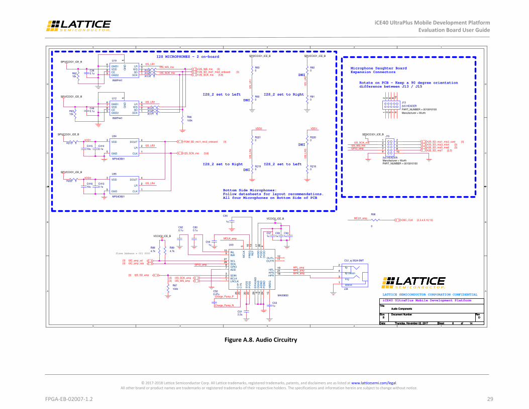
Figure A.8. Audio Circuitry
5
5
4
4
3
3
2
2
1
1
D D
C C
B B
A A
LATTICE SEMICONDUCTOR CORPORATION CONFIDENTIAL
Microphone Daughter BoardExpansion Connectors
iCE40 UltraPlus Mobile Development Platform
Rotate on PCB - Keep a 90 degree orientation difference between J13 / J15
Slave Address = 001 0000
I2S MICROPHONES - 2 on-board
Bottom Side Microphones:Follow datasheets for layout recommendations.All four Microphones on Bottom Side of PCB
DNI
I2S_2 set to Right
DNI
I2S_2 set to Left
DNI
I2S_2 set to Left
DNI
I2S_2 set to Right
VCCIO2_iCE_B
VCCIO2_iCE_B
SPIVCCIO1_iCE_B
SPIVCCIO1_iCE_B SPIVCCIO1_iCE_B
SPIVCCIO1_iCE_B
SPIVCCIO1_iCE_B
SPIVCCIO1_iCE_B
SPIVCCIO1_iCE_B
OSC_CLK {2,3,4,5,10,13}
I2S_SD_mic1_mic2_card {3}I2S_SD_mic3_mic4 {3}I2S_SD_mic5_mic6 {3}I2S_SD_mic7 {2,3}
I2S_SD_amp{3}I2S_SCK_amp{3}I2S_WS_amp{3}
I2C_amp_scl{3}I2C_amp_sda{3}
I2S_SCK_mic {3,8}I2S_SD_mic1_mic2_onboard {3}I2S_WS_mic {3}
I2S_SCK_mic {3,8}
PDM_SD_mic1_mic2_onboard {3}
Title
Size Document Number Rev
Date: Sheet of
D
Audio Components
B
8 14Thursday, November 02, 2017
Title
Size Document Number Rev
Date: Sheet of
D
Audio Components
B
8 14Thursday, November 02, 2017
Title
Size Document Number Rev
Date: Sheet of
D
Audio Components
B
8 14Thursday, November 02, 2017
R175 0
C531u
C41610u
J34
CUI_sj-3524-SMT
1sleeve
3ring
4tip switch
2tip
R66100k
R2180
R894.7k
U95
MP34DB01
CLK1
LR2
GND5
VDD3
DOUT4
R6210k
R2190
R96
0
U19
INMP441
SCK1SD2WS3LR4
GN
D5
GND16
VDD7
CE8
GND29
U43
MAX9850
LRCLK1 BCLK2 SDIN3
DV
DD
4
MC
LK5
DG
ND
6
ADD7 GPIO8
INR9 INL
10
OUTR11OUTL12R
EF
13
AG
ND
14
NR
EG
15
PR
EG
16
AV
DD
17
HPR18
HPL19
SV
SS
20
HPS21
PV
SS
22
C1N
23
PG
ND
24
C1P
25
PV
DD
26SCL
27
SDA28
EP
AG
ND
29
C571u
R800
C360.1u
R6310k
C55
1u
R2200
C600.1u
C4130.1u
C591u
R810
R2210
R171 0
C931u
R820
R222 0
C512.2u
U12
INMP441
SCK1SD2WS3LR4
GN
D5
GND16
VDD7
CE8
GND29
R830
R172 0
C541u
R87100k
R884.7k
U94
MP34DB01
CLK1
LR2
GND5
VDD3
DOUT4
C460.1u
R173 0
C520.47u
C920.1u
R213 0
R174 0
C4140.1u
J132x5 HEADERPART_NUMBER = 0015910100Manufacturer = Wurth
2 4 6 8 1097531
C41510u
J15
2x5 HEADER
PART_NUMBER = 0015910100Manufacturer = Wurth
2468109
7531
R176 0
I2S_SCK_micI2S_WS_mic
HPS_amp
MCLK_amp
MCLK_amp
Charge_Pump_P
Charge_Pump_N
HPR_amp
HPL_amp
GPIO_amp
GPIO_amp
I2S_LR1I2S_WS_mic
I2S_SCK_mic
I2S
_LR
1
I2S
_LR
2
I2S_LR2
I2S
_LR
4
I2S
_LR
3
I2S_LR3
I2S_LR4
VDD2 VDD1
VDD1
VDD2
iCE40 UltraPlus Mobile Development Platform Evaluation Board User Guide
© 2017-2018 Lattice Semiconductor Corp. All Lattice trademarks, registered trademarks, patents, and disclaimers are as listed at www.latticesemi.com/legal. All other brand or product names are trademarks or registered trademarks of their respective holders. The specifications and information herein are subject to change without notice.
30 FPGA-EB-02007-1.2
Figure A.9. Sensor & RGB Circuitry
5
5
4
4
3
3
2
2
1
1
D D
C C
B B
A A
Notes:- Gyro and Accelerometer interfaces are both set to I2C- I2C address LSB for Gyro is '1' and for Accelerometer is '0' Gyro = 1101011 Accel = 0011000- SPI for both Gyro and Accelerometer is disabled
GYROSCOPE SENSOR
PRESSURE SENSOR
COMPASS SENSOR
LATTICE SEMICONDUCTOR CORPORATION CONFIDENTIAL
ACCELEROMETER w/ FIFO
RGB LED
Resistor switch to SPARE I/O
Slave Address = 001 1101Pull-down can switch to 001 1110
Slave Address = 1110111
Accel Slave Address = 001 1001Magnetometer Slave Address = 001 1110
PMOD Connector
(note VCC is 1V8, PMOD expects 3V3)
iCE40 UltraPlus Mobile Development Platform
VCCIO2_iCE_C
VCC3V3
VCCIO2_iCE_C
VCCIO2_iCE_C
VCC3V3VCCIO2_iCE_C
VCCIO2_iCE_C
VCCIO2_iCE_C
VCCIO2_iCE_C
VCC3V3_PMOD VCC3V3_PMOD
VCCIO2_iCE_C
GLED{4}
RLED{4}
BLED {4}
RGB_ANODE {4}I2C_sensor_SDA {4}I2C_sensor_SCL {4}
SPARE_C0{4,13}SPARE_C1{4,13}
SPARE_C4 {4,13}
SPARE_C5 {4,13}SPARE_C3{4,13}SPARE_C2{4,13}
Title
Size Document Number Rev
Date: Sheet of
D
Sensors & RGB Circuitry
B
9 14Thursday, November 02, 2017
Title
Size Document Number Rev
Date: Sheet of
D
Sensors & RGB Circuitry
B
9 14Thursday, November 02, 2017
Title
Size Document Number Rev
Date: Sheet of
D
Sensors & RGB Circuitry
B
9 14Thursday, November 02, 2017
C770.1u
C5010u
R108 0 DNI
R1210k
C7310u
R132 0 DNI
R162 0 DNI
C630.1u
C74100n
U22
BMP180
NC11
VDD2
VDDIO3
NC44SCL5SDA6
GND7
C644.7u
C791u
C650.22u
R164 0 DNI
LSM303DLHCU35
C16
RES110
RES211
SETP12
SETC13
SCL2
SDA3
INT24
INT15
DRDY9
VD
DIO
1
VD
D14
GN
D7
NC
8
R112 0DNI
C16100n
U36LSM330DLC
RES02
GND01
RE
S8
14
RE
S7
13
RE
S6
12
RE
S5
11
RE
S4
10
VD
D0
7
CAP15
DEN_G16
DRDY_G/INT2_G17
INT1_G18
INT2_A19
INT1_A20
VD
D_I
O_0
21
CS
_G22
CS
_A23
SC
L_A
/G24
VD
D_I
O_1
25
SD
O_G
26
RES13RES24RES35GND16V
DD
18
VD
D2
9
SD
O_A
27
SD
A_A
/G28
R163 0 DNI
R1014.7k
R165 0 DNI
R110 0 DNI
R810k
R13
0
R1024.7k
R114 0
DNI
R9DNP
U38
LIS2DS12
SCL/SPC1
CS2
SDO/SA03
SDA/SDI/SDO4
NC
5G
ND
16
RES7 GND08 VDD9 VDD_IO
10 INT
211
INT
112
C611u
J8
PMOD Connector
DNI
12345
7891011
6 12
D13
150141M173100
A1
R3
G4
B2
C620.1u
R107 0 DNI
C250.1u
C490.1u
C72100nF
I2C_sensor_SDAI2C_sensor_SCL
I2C_sensor_SCLI2C_sensor_SDA
I2C_sensor_SCL
I2C_sensor_SDA
I2C_sensor_SDA
I2C_sensor_SCL
Acc
el_I
nt2
Acc
el_I
nt1
Accel_Int1Accel_Int2
I2C_sensor_SCL I2C_sensor_SDA
I2C_sensor_SDA
I2C_sensor_SCL
I2C_sensor_SDAI2C_sensor_SCL

iCE40 UltraPlus Mobile Development Platform Evaluation Board User Guide
© 2017-2018 Lattice Semiconductor Corp. All Lattice trademarks, registered trademarks, patents, and disclaimers are as listed at www.latticesemi.com/legal. All other brand or product names are trademarks or registered trademarks of their respective holders. The specifications and information herein are subject to change without notice.
FPGA-EB-02007-1.2 31
Figure A.10. Camera Circuitry
5
5
4
4
3
3
2
2
1
1
D D
C C
B B
A A
LATTICE SEMICONDUCTOR CORPORATION CONFIDENTIAL
0201 0201 0201
XVCLK = 27 MHz
EN_HI = 1.3VOVM7692 -> DOVDD then AVDD (10 ms max delay)
iCE40 UltraPlus Mobile Development Platform
Resistor Switch for Parallel Video Support
Slave Address = 011 1100
Camera Expansion Connector
VCCIO2_iCE_D
VCCIO2_iCE_D
VCC1V5
VCC2V8VSUPPLY_CAM
VCC1V5 VCC2V8
VCCIO2_iCE_DVCCIO2_iCE_D
VSUPPLY
VCC3V3
VCC1V8
VSUPPLY VCC3V3 VCC1V8
CSI_HS_CLKP {5}CSI_HS_CLKN {5}CSI_HS_D0P {5}CSI_HS_D0N {5}
SPARE_D1 {5,13}
SPARE_D2 {5,13}
SPARE_D0 {5,13}
I2C_camera_scl {5}I2C_camera_sda {5}
proc_cs {2,3,4,5,6}
proc_intr {2,3,4,5,6}
OSC_CLK {2,3,4,5,8,13}
CAM_D3 {5}
CAM_D2 {5}
iCE_SI_D {5,6}iCE_SO_D {5,6}
LDO_CE_VDC {7,12}
UART_RX {2,3,4,5,6,13}UART_TX {2,3,4,5,6,13}
iCE_SCK_D{5,6}iCE_SS_D{5,6}
CRSTb {2,3,4,5,6,11,13}
Title
Size Document Number Rev
Date: Sheet of
D
Camera Circuitry
B
10 14Friday, November 03, 2017
Title
Size Document Number Rev
Date: Sheet of
D
Camera Circuitry
B
10 14Friday, November 03, 2017
Title
Size Document Number Rev
Date: Sheet of
D
Camera Circuitry
B
10 14Friday, November 03, 2017
C169
0.1uF
DNI
C850.1u
U16
Hirose - FX12 - 40 Pos
DNI
CH0_DCK_P1
CH0_DCK_N2
GND3
CH0_DATA0_P4
CH0_DATA0_N5
GND6
CH0_DATA2_P7
CH0_DATA2_N8
GND9
SN10
SCLK11
PWR_12V12
SDA113
SCL114
GND15
CH2_DATA0_P16
CH2_DATA0_N17
GND18
CH2_DCK_P19
CH2_DCK_N20
PWR_12-0V21
RESETN22
PWR_5-0V23
CH0_DATA1_P24
CH0_DATA1_N25
PWR_3-3V26
CH0_DATA3_P27
CH0_DATA3_N28
PWR_1-8V29
MOSI30
MISO31
PWR_1-8V32
GND33
GND34
PWR_3-3V35
CH2_DATA1_P36
CH2_DATA1_N37
PWR_5-0V38
SDA39
SCL40
Shield141
Shield242
Shield343
Shield444 Shield5
45
Shield646
C1290.47uC86
0.1u
R135 0 DNI
R43 0
R55 0
R138 0 DNI
R1054.7k
C170
0.1uF
DNI
C760.1u
AP7346D-1528FS6-7
U44
1.5VO1
1.5EN6
2.8EN4
2.8VO2
VIN
5G
ND
3
EP
AD
7
R133 0 DNI
C910.47u
R53 0
C750.1u
R136 0 DNI
R52 0
C168
0.1uF
DNI
R56 0
R60 0
R140 0 DNI
R54 0
R1064.7k
R59 0
C1300.47u
R139 0 DNI R134 0 DNI
R137 0 DNI
C870.1u
U39
OVM7692
NC0A1 AVDDA2
NC1B4
VREF1A4
VREF2B3
AGNDA3
DV
DD
E4
DO
VD
DD
4
DO
GN
DC
2
PW
DN
B1
SIO
CC
1
SO
IDB
2
D2E2
D3D2
D4/MCPD5
D5/MCNC5
D6/MDPA5
D7/MDNB5
EGNDC4
XV
CLK
E5
HR
EF
E1
PC
LKD
3
VS
YN
CD
1
D0
E3
D1
C3
11
22
33
44
CA
M_X
CLK
CA
M_H
RE
FC
AM
_PC
LKC
AM
_VS
YN
CC
AM
_D0
CA
M_D
1
CAM_D2CAM_D3CAM_MCP_D4CAM_MCN_D5CAM_MDP_D6CAM_MDN_D7
I2C
_cam
era_
scl
I2C
_cam
era_
sda
CAM_MCP_D4CAM_MCN_D5CAM_MDP_D6CAM_MDN_D7
I2C_camera_sclI2C_camera_sda
CAM_D1
CAM_D0
CAM_PCLK
CAM_VSYNC
CAM_HREF
CAM_XCLK
I2C_camera_sda I2C_camera_scl
CAM_D3
CAM_D2
CAM_XCLK
I2C_camera_sdaI2C_camera_scl
CAM_MCP_D4CAM_MCN_D5
CAM_MDP_D6CAM_MDN_D7
CAM_D2CAM_D3
CAM_D0CAM_D1
CAM_VSYNCCAM_HREF

iCE40 UltraPlus Mobile Development Platform Evaluation Board User Guide
© 2017-2018 Lattice Semiconductor Corp. All Lattice trademarks, registered trademarks, patents, and disclaimers are as listed at www.latticesemi.com/legal. All other brand or product names are trademarks or registered trademarks of their respective holders. The specifications and information herein are subject to change without notice.
32 FPGA-EB-02007-1.2
Figure A.11. USB Programming
5
5
4
4
3
3
2
2
1
1
D D
C C
B B
A A
FTDI PROGRAMMER
USB - POWER & PROGRAMMING
LATTICE SEMICONDUCTOR CORPORATION CONFIDENTIAL
iCE40 UltraPlus Mobile Development Platform
VCC3V3
VCC3V3
VCC3V3
FTVCOR
VCC3V3
FTVCOR
VCC3V3
FTVCOR
FTVCOR
VCC3V3
VCC3V3
VCC3V3
USB5VVCC3V3
USB5VCRSTb{2,3,4,5,6,10,13}
flsh_miso{6}iCE_SCK{6}iCE_SS{6,13}flsh_mosi{6}
CDONE{2,3,4,5,6}
FT_RESETb{6}
UART_RX_D {5}UART_TX_D {5}
Title
Size Document Number Rev
Date: Sheet of
D
USB Programming
B
11 14Thursday, November 02, 2017
Title
Size Document Number Rev
Date: Sheet of
D
USB Programming
B
11 14Thursday, November 02, 2017
Title
Size Document Number Rev
Date: Sheet of
D
USB Programming
B
11 14Thursday, November 02, 2017
R250 C3130.1u
C3733p
C480.1u
C304.7u
C220.1u
C470.1u
Y1
12MHz
R210
R23
470
5VD-D+IDG
USB PWRJ5
1234
S2
5
S1S3
S4
R201k
R16 10
C2333p
U93
ESDR0502PART_NUMBER = ESDR0502NMUTBGManufacturer = ON Semi
GND1
NC22
NC33
D-4
D+5
VBUS6
C2110u
R1110k
R260
C200.1u
L3
600 ohm, 500 mA
R280
R270L1
600 ohm, 500 mA
R1812k
93LC56BT-I/OTU6
GND2
VCC6 DO
1
DI3
CLK4
CS5
R16610k
C290.1u
L2600 ohm, 500 mA
R16710k
C1847u
C190.1u
R240
U9
FT2232H
Gnd_11
OSCI2
OSCO3
VPHY4
Gnd_75
REF6
DM7
DP8
VPLL9
AGnd10
Gnd11
VCORE_112
TEST13
RESET#14
Gnd_215
ADBUS016
AD
BU
S1
17
AD
BU
S2
18
AD
BU
S3
19
VC
CIO
20
AD
BU
S4
21
AD
BU
S5
22
AD
BU
S6
23
AD
BU
S7
24
Gnd
_325
AC
BU
S0
26
AC
BU
S1
27
AC
BU
S2
28
AC
BU
S3
29
AC
BU
S4
30
VC
CIO
_331
AC
BU
S5
32
ACBUS633ACBUS734Gnd_435SUSPEND#36VCORE37BDBUS038BDBUS139BDBUS240BDBUS341VCCIO_242BDBUS443BDBUS544BDBUS645BDBUS746Gnd_547BCBUS048
VR
EG
OU
T49
VR
EG
IN50
Gnd
_651
BC
BU
S1
52B
CB
US
253
BC
BU
S3
54B
CB
US
455
VC
CIO
_156
BC
BU
S5
57B
CB
US
658
BC
BU
S7
59P
WR
EN
#60
EE
DA
TA
61E
EC
LK62
EE
CS
63V
CO
RE
_364
R102k2
C440.1u
C240.1u
R17 10
C380.1u
C434.7u
USB_DM
GND
FT_CRST
EP
_CS
FT_CRST
GN
D
EP_DI
GN
D
EP_CLK
EP_CS
GND
FT_DI
FT_DIFT_SK
FT_SK
FT_CS
EP
_DI
FT_DO
FT_CS
EP
_CLK
GND
USB_DP
GND
FT_DO
GND
GND
US
B_D
P
US
B_D
M
FT_CDONE
FT_CDONE
USB_DP
USB_DM
USB_DP
USB_DM
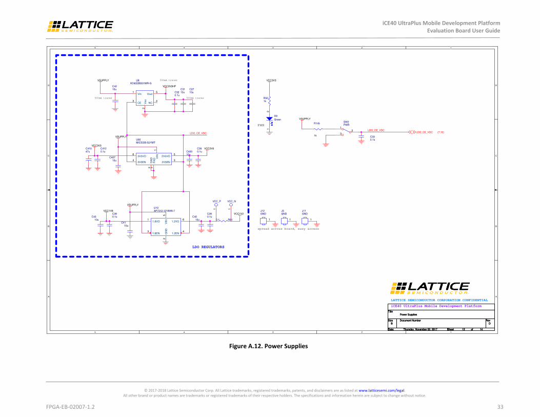
iCE40 UltraPlus Mobile Development Platform Evaluation Board User Guide
© 2017-2018 Lattice Semiconductor Corp. All Lattice trademarks, registered trademarks, patents, and disclaimers are as listed at www.latticesemi.com/legal. All other brand or product names are trademarks or registered trademarks of their respective holders. The specifications and information herein are subject to change without notice.
FPGA-EB-02007-1.2 33
Figure A.12. Power Supplies
5
5
4
4
3
3
2
2
1
1
D D
C C
B B
A A
spread across board, easy access
LDO REGULATORS
500mA traces 500mA traces
500mA traces
PWR
LATTICE SEMICONDUCTOR CORPORATION CONFIDENTIAL
iCE40 UltraPlus Mobile Development Platform
VSUPPLY
VCC1V2VCC1V8
VCC2V5VCC3V3
VSUPPLY
VCC3V3
VCC3V3HP
VSUPPLY
VSUPPLY
LDO_CE_VDC {7,10}
Title
Size Document Number Rev
Date: Sheet of
D
Power Supplies
B
12 14Thursday, November 02, 2017
Title
Size Document Number Rev
Date: Sheet of
D
Power Supplies
B
12 14Thursday, November 02, 2017
Title
Size Document Number Rev
Date: Sheet of
D
Power Supplies
B
12 14Thursday, November 02, 2017
AP7312-1218W6-7U10
1.8VO1
1.8EN3
1.2EN4
1.2VO6
VIN
5G
ND
2
J11GND
1
J12GND
1
C40010u
D9Green
21
VCC_P
1
C260.1u
C4010u
C280.1u
C4210u
VCC_N
1
C4510u
C40710u
C3110u
C4110u
U8XC6222B331MR-G
Vin1
Vss
2
CE3
NC4
Vout5
J3GND
1
R501k
C330.1u
C4120.1u
R145
1k
U90MIC5335-SJYMT
VIN
1
GN
D2
2V5EN3
3V3EN4
2V5VO5
3V3VO6
PA
D7
R610.1
SW2PWR
21
3
C41047u
C390.1u
C320.1u
C2710u
LDO_CE_VDCLDO_CE_VDC

iCE40 UltraPlus Mobile Development Platform Evaluation Board User Guide
© 2017-2018 Lattice Semiconductor Corp. All Lattice trademarks, registered trademarks, patents, and disclaimers are as listed at www.latticesemi.com/legal. All other brand or product names are trademarks or registered trademarks of their respective holders. The specifications and information herein are subject to change without notice.
34 FPGA-EB-02007-1.2
Figure A.13. Common Components
5
5
4
4
3
3
2
2
1
1
D D
C C
B B
A A
LATTICE SEMICONDUCTOR CORPORATION CONFIDENTIAL
PB1
CLOCK OSCILLATOR
PB2
SPARE_A1 shared with Display Controls (LED is default)SPARE_A0 shared with Display Controls (PB is default)
SPARE_A2 shared with Display Controls (LED is default)
SPARE_D1 shared with Camera Parallel Interfaces (LED is default)SPARE_D0 shared with Camera Parallel Interface (PB is default)
SPARE_D2 shared with Camera Parallel Interface (LED is default)
SPARE_C1 shared with Accel interrupt2 (SW is default)SPARE_C0 shared with Accel interrupt1 (PB is default)
SPARE_C2 shared with PMOD (PB is default)SPARE_C0 shared with PMOD (SW is default)SPARE_C0 shared with PMOD (LED is default)SPARE_C0 shared with PMOD (LED is default)
Common Control Headers
iCE40 UltraPlus Mobile Development Platform
FPGA_C GPIO LED2 LED1
Common Spare Signals
VCC3V3
VCC3V3VCCIO2_iCE_C
SPIVCCIO1_iCE_C
VCC3V3
VCCIO2_iCE_C
SPARE_A0 {2,7}SPARE_A1 {2,7}SPARE_A2 {2,7}
SPARE_D0 {5,10}SPARE_D1 {5,10}SPARE_D2 {5,10}
SPARE_C0 {4,9}SPARE_C1 {4,9}SPARE_C2 {4,9}SPARE_C3 {4,9}SPARE_C4 {4,9}SPARE_C5 {4,9}
OSC_CLK {2,3,4,5,8,10}UART_RX {2,3,4,5,6,10}UART_TX{2,3,4,5,6,10}
CRSTb {2,3,4,5,6,10,11}
iCE_SS {6,11}M25P80_CSn{6}
SWCLK{6} SWDIO {6}
Title
Size Document Number Rev
Date: Sheet of
D
Common Components
B
13 14Friday, November 03, 2017
Title
Size Document Number Rev
Date: Sheet of
D
Common Components
B
13 14Friday, November 03, 2017
Title
Size Document Number Rev
Date: Sheet of
D
Common Components
B
13 14Friday, November 03, 2017
R125 0 DNISW8A
SW_SPST_2
1 4
ASFLMB-27.000MHZ-LC-TU14
GND2
VDD4
STDBY#1
OUT3
D7Red
21
R128 0
R58470
R9710k
C1350.1u
R130 0
R98 4.7K
R121 0
R1410k
D2Green
21
J28
Common Control
246810
13579
SW6PB
R126 0 DNI
SW8B2 3
R124 0
R7910k
C560.1u
R50
R123 0
R122 0
R57470
C1340.1u
R99 4.7K
SW7PB
R127 0 DNI
J23Clock Source Sel
123
R129 0
R131 0
R120 0
OSC_CLK_stndby#
PB2
SW1
SW2
LED1
LED1LED2
LED1PB1
LED2
LED2SW1PB2SW2
OSC_CLK_stndby#

iCE40 UltraPlus Mobile Development Platform Evaluation Board User Guide
© 2017-2018 Lattice Semiconductor Corp. All Lattice trademarks, registered trademarks, patents, and disclaimers are as listed at www.latticesemi.com/legal. All other brand or product names are trademarks or registered trademarks of their respective holders. The specifications and information herein are subject to change without notice.
FPGA-EB-02007-1.2 35
Figure A.14. Battery Connector ŀƴŘ Charger
5
5
4
4
3
3
2
2
1
1
D D
C C
B B
A A
Iterm is set to be 25 mA.Default timings are used for timer programming. 5-hour fast charge and 30-minute precharge
Input Current Limit is set to be 500 mAFast-charge current is set to be 200 mA
LATTICE SEMICONDUCTOR CORPORATION CONFIDENTIALLATTICE SEMICONDUCTOR CORPORATION CONFIDENTIAL
iCE40 UltraPlus Mobile Development Platform
Through hole test pads for battery soldering
USB
DRGN5V
USB5V
VSUPPLY
BT_3V7
BT_3V7
USB5VBT_3V7
BT_3V7BT_3V7
Title
Size Document Number Rev
Date: Sheet of
D
Battery Connector & Charger
B
14 14Thursday, November 02, 2017
Title
Size Document Number Rev
Date: Sheet of
D
Battery Connector & Charger
B
14 14Thursday, November 02, 2017
Title
Size Document Number Rev
Date: Sheet of
D
Battery Connector & Charger
B
14 14Thursday, November 02, 2017
R511K
R04025%
TP12 80_MIL_PAD1
TP13 80_MIL_PAD1
BQ24232
U15
BQ24232Manufacturer = TIPART_NUMBER = BQ24232RGTT
TS1
BAT12
BAT23
CE_L4
EN25
EN16
PGOOD_L7
VSS8
CHG_L9
OUT110
OUT211IN
13
EPAD17
TMR14
ITERM15
ILIM12
ISET16
C940.1uF16VC0402
D3PMEG2010AEH
R642K
R04025% R3
10K
R04025%
12
D4PMEG2010AEH
C954.7uF10VC0402
D8Green
21
C960.1uF16VC0402
R924.32K
R04021%
C151uF
C040216V
R932.94K
R04021%
C580.1uF16VC0402
D5YELLOW
Manufacturer = Lite-O
NP
AR
T_N
UM
BE
R = LT
ST
-C193K
SK
T-5A
21
R943.57K
R04021%
R95DNLR0402D6
GREEN
Manufacturer = O
SR
AM
PA
RT
_NU
MB
ER
= LG L29K
-G2J1-24-Z
21
R1461k
C904.7uF10VC0402

iCE40 UltraPlus Mobile Development Platform Evaluation Board User Guide
© 2017-2018 Lattice Semiconductor Corp. All Lattice trademarks, registered trademarks, patents, and disclaimers are as listed at www.latticesemi.com/legal. All other brand or product names are trademarks or registered trademarks of their respective holders. The specifications and information herein are subject to change without notice.
36 FPGA-EB-02007-1.2
Appendix B. iCE40 UltraPlus Mobile Development Board Bill of Materials
Item Reference Qty Part PART_NUMBER Manufacturer Description
1
C1, C6, C9, C12, C88, C98, C102, C106, C108, C111, C115, C117, C119, C122, C124, C127
16 10n GRM033R61C103KA12D Murata CAP CER 10000PF 16V 10% X5R 0201
2
C2, C5, C8, C10, C13, C34, C78, C81, C83, C89, C99, C101, C105, C109, C110, C114, C120, C121, C126, C133
20 0.1u GRM033R61A104KE15D Murata CAP CER 0.1UF 10V X5R 0201
3
C3, C4, C11, C14, C35, C53, C54, C55, C57, C59, C61, C79, C80, C82, C84, C93, C97, C103, C107, C112, C116, C118, C123, C128
24 1u 885012105012 Wurth CAP CER 1UF 10V X5R 0402
4 C7, C73, C104, C113, C125
5 10u CL05A106MP5NUNC Samsung CAP CER 10UF 10V X5R 0402
5 C15 1 1uF C1005X5R1C105K050BC TDK CAP CER 1UF 16V 10% X5R 0402
6 C16 1 100n 885012205037 Wurth CAP CER 0.1UF 16V X7R 0402
7
C17, C19, C20, C22, C24, C25, C26, C28, C29, C32, C33, C36, C38, C39, C44, C47, C48, C49, C56, C60, C62, C63, C75, C76, C77, C85, C86, C87, C92, C100, C134, C135, C313, C409, C412, C414, C417, C418
38 0.1u 885012105010 Wurth CAP CER 0.1UF 10V X5R 0402
8 C18, C410 2 47u TCJB476M010R0070 AVX CAP TANT POLY 47UF 10V 1210
9 C21, C27, C31, C40, C45, C400
6 10u CL10A106MQ8NNNC Samsung CAP CER 10UF 6.3V X5R 0603
10 C23, C37 2 33p 885012005058 Wurth CAP CER 33PF 50V NP0 0402
11 C30, C43, C64 3 4.7u CC0603KRX5R6BB475 Yageo CAP CER 4.7UF 10V X5R 0603
12 C41, C42, C407 3 10u CL10X106MP8NRNC Samsung CAP CER 10UF 10V X6S 0603
13 C46, C413 2 0.1u 885012105010 Wurth CAP CER 0.1UF 10V X5R 0402
14 C50 1 10u CL10X106MP8NRNC Samsung CAP CER 10UF 10V X6S 0603

iCE40 UltraPlus Mobile Development Platform Evaluation Board User Guide
© 2017-2018 Lattice Semiconductor Corp. All Lattice trademarks, registered trademarks, patents, and disclaimers are as listed at www.latticesemi.com/legal. All other brand or product names are trademarks or registered trademarks of their respective holders. The specifications and information herein are subject to change without notice.
FPGA-EB-02007-1.2 37
Item Reference Qty Part PART_NUMBER Manufacturer Description
15 C51 1 2.2u C1005X5R1C225K050BC TDK CAP CER 2.2UF 16V 10% X5R 0402
16 C52, C91, C129, C130
4 0.47u C1005X5R1E474K050BB TK CAP CER 0.47UF 25V X5R 0402
17 C58, C94, C96 3 0.1uF 885012105016 Wurth CAP CER 0.1UF 16V X5R 0402
18 C65 1 0.22u 885012206048 Wurth CAP CER 0.22UF 16V X7R 0603
19 C66 1 0.1uF 885012105016 Wurth CAP CER 0.1UF 16V X5R 0402
20 C67, C68, C69 3 1uF GRM155R61C105KE01D Murata CAP CER 1UF 16V 10% X5R 0402
21 C70 1 1uF 885012208093 Wurth CAP CER 1UF 50V X7R 1206
22 C71 1 1uF GRM155R61C105KE01D Murata CAP CER 1UF 16V 10% X5R 0402
23 C72 1 100nF 885012105016 Wurth CAP CER 0.1UF 16V X5R 0402
24 C74 1 100n 885012105016 Wurth CAP CER 0.1UF 16V X5R 0402
25 C90, C95 2 4.7uF C1005X5R1A475K050BC TDK CAP CER 4.7UF 10V 10% X5R 0402
26 C168, C169, C170 3 0.1uF 885012105016 Wurth CAP CER 0.1UF 16V X5R 0402
27 C415, C416 2 10u CL10X106MP8NRNC Samsung CAP CER 10UF 10V X6S 0603
28 D1, D11, D12, D14 4 GREEN 150060GS75000 Wurth LED GREEN CLEAR 0603 SMD
29 D2 1 Green 150060GS75000 Wurth LED GREEN CLEAR 0603 SMD
30 D3, D4 2 PMEG2010AEH PMEG2010AEH, 115 NXP Semiconductor
DIODE SCHOTTKY 20V 1A SOD123F
31 D5 1 YELLOW 150060YS75000 Wurth LED YELLOW RECT CLEAR 0603
32 D6 1 GREEN 150060GS75000 Wurth LED SMARTLED GREEN 570NM 0603
33 D7 1 Red 150060SS75000 Wurth LED RED CLEAR 0603 SMD
34 D8, D9 2 Green 150060VS75000 Wurth LED SUPER GREEN CLEAR 0603 SMD
35 D13 1 150141M173100 150141M173100 Wurth LED RGB CLEAR 1411 SMD
36 J2 1 503548-1220 5035481220 Molex Inc CONN RCPT BTB 12POS DL VERT SMD
37 J3, J11, J12 3 GND 608001162100 Wurth
38 J5 1 USB PWR 65100516121 Wurth CONN COM TYPE B MINI USB SMD 5P
39 J8 1 PMOD Connector - - CONN HEADER .100 DUAL STR 10POS
40 J13, J15 2 2x5 HEADER 61001021121 Wurth CONN HEADER VERT DUAL 10POS 2.54
41 J16 1 AP INTERCONNECT
62101021921 Wurth 2.00 mm SMT Dual Pin Header
42 J17, J26, J27 3 iCEA Control 62101021921 Wurth 2.00 mm SMT Dual Pin Header
43 J18 1 BLE PROG SEL 62000311121 Wurth 2.00 mm THT Pin Header

iCE40 UltraPlus Mobile Development Platform Evaluation Board User Guide
© 2017-2018 Lattice Semiconductor Corp. All Lattice trademarks, registered trademarks, patents, and disclaimers are as listed at www.latticesemi.com/legal. All other brand or product names are trademarks or registered trademarks of their respective holders. The specifications and information herein are subject to change without notice.
38 FPGA-EB-02007-1.2
Item Reference Qty Part PART_NUMBER Manufacturer Description
44 J19 1 A3A-04PA-2SV(71)
A3A-4PA-2SV(71) Hirose CONN HEADER 2mm DUAL STR 4POS SMT
45 J23 1 Clock Source Sel 62000311121 Wurth 2.00 mm THT Pin Header
46 J25 1 iCEA Control 57202-G52-06LF Amphenol FCI
12 Positions Header, Unshrouded Connector 0.079" (2.00mm) Surface Mount Gold, GXT™
47 J28 1 Common Control 62101021921 Wurth 2.00 mm SMT Dual Pin Header
48 J30, J32 2 CON24A — — —
49 J31, J33 2 CON24A — — —
50 J34 1 CUI_sj-3524-SMT SJ-3524-SMT-TR CUI Inc. CONN AUDIO JACK 3.5MM STEREO SMD
51 L1, L2, L3 3 600 Ohm, 500 mA
MMZ1608R601A TDK FERRITE BEAD 600 OHM 0603 1LN
52 L4 1 22uH AIML-0805HC-220M-T Abracon Corporation
HIGH CURRENT CHIP IND 22.0UH 20%
53 R1, R84, R85, R86 4 100 RC1005J101CS Samsung RES 100 OHM 1/16W 5% 0402
54 R2, R49, R69, R70 4 2k2 RC1005J222CS Samsung RES 2.2K OHM 1/16W 5% 0402
55 R3 1 10K ERJ-2RKF1002X Panasonic RES 10K OHM 1/10W 1% 0402 SMD
56 R4, R6, R7, R8, R12, R62, R63, R65, R200
9 10k ERJ-2RKF1002X Panasonic RES 10K OHM 1/10W 1% 0402 SMD
57 R5 1 0 ERJ-3GEY0R00V Panasonic RES SMD 0.0 OHM JUMPER 1/10W 0603
58 R9 1 DNP — — —
59 R10 1 2k2 RC1005J222CS Samsung RES 2.2K OHM 1/16W 5% 0402
60 R11, R14, R79, R97, R166, R167
6 10k ERJ-2RKF1002X Panasonic RES 10K OHM 1/10W 1% 0402 SMD
61
R13, R29, R35, R37, R40, R76, R77, R205, R206, R224
10 0 ERJ-2GE0R00X Panasonic RES 0.0 OHM 1/10W 0402 SMD
62
R15, R19, R22, R30, R47, R56, R59, R60, R81, R83, R96, R141, R142, R143, R147, R148, R149, R150, R152, R153, R154, R155, R157, R158, R159, R160, R168, R169, R170, R171, R172, R173, R174, R175, R176, R213, R218, R221, R222
39 0 ERJ-3GEY0R00V Panasonic RES SMD 0.0 OHM JUMPER 1/10W 0603

iCE40 UltraPlus Mobile Development Platform Evaluation Board User Guide
© 2017-2018 Lattice Semiconductor Corp. All Lattice trademarks, registered trademarks, patents, and disclaimers are as listed at www.latticesemi.com/legal. All other brand or product names are trademarks or registered trademarks of their respective holders. The specifications and information herein are subject to change without notice.
FPGA-EB-02007-1.2 39
Item Reference Qty Part PART_NUMBER Manufacturer Description
63 R16, R17 2 10 RC1005J100CS Samsung RES 10 OHM 1/16W 5% 0402
64 R18 1 12k RC1005F123CS Samsung RES 12K OHM 1/16W 1% 0402
65 R20, R50, R145, R146
4 1k RC1005J102CS Samsung RES 1K OHM 1/16W 5% 0402
66 R21, R24, R25, R26, R27, R28
6 0 RC1005J000CS Samsung RES 0.0 OHM 1/16W JUMP 0402
67 R23 1 470 RC1005J471CS Samsung RES 470 OHM 1/16W 5% 0402
68 R31 1 0 ERJ-2GE0R00X Panasonic RES 0.0 OHM 1/10W 0402 SMD
69
R32, R43, R52, R53, R54, R55, R107, R108, R110, R132, R133, R134, R135, R136, R137, R138, R139, R140, R162, R163, R164, R165
22 0 ERJ-3GEY0R00V Panasonic RES SMD 0.0 OHM JUMPER 1/10W 0603
70 R33, R36, R72 3 30 ERJ-1GEJ300C Panasonic RES 30 OHM 1/20W 5% 0201 SMD
71 R34, R38, R39, R71 4 1K ERJ-1GEF1001C Panasonic RES SMD 1K OHM 1% 1/20W 0201
72 R41 1 10k ERJ-2GEJ103X Panasonic RES SMD 10K OHM 5% 1/10W 0402
73 R42 1 18 ERJ-2GEJ180X Panasonic RES SMD 18 OHM 5% 1/10W 0402
74 R44 1 0 ERJ-2GE0R00X Panasonic RES SMD 0.0 OHM JUMPER 1/10W 0402
75 R45, R48, R67, R68, R75, R223
6 0 ERJ-2GE0R00X Panasonic RES 0.0 OHM 1/10W 0402 SMD
76 R46 1 30 ERJ-1GEJ300C Panasonic RES 30 OHM 1/20W 5% 0201 SMD
77 R51 1 1K ERJ-2GEJ102X Panasonic RES SMD 1K OHM 5% 1/10W 0402
78 R57, R58 2 470 ERJ-3GEYJ471V Panasonic RES SMD 470 OHM 5% 1/10W 0603
79 R61 1 0.1 RUT1005FR100CS Samsung RES SMD 0.1 OHM 1% 1/10W 0402
80 R64 1 2K ERJ-2GEJ202X Panasonic RES SMD 2K OHM 5% 1/10W 0402
81 R66, R87, R203 3 100k RC1005J104CS Samsung RES SMD 100K OHM 5% 1/16W 0402
82 R73, R100 2 100 ERJ-1GEF1000C Panasonic RES SMD 100 OHM 1% 1/20W 0201
83 R74, R78, R98, R99 4 4.7K ERJ-3EKF4701V Panasonic RES SMD 4.7K OHM 1% 1/10W 0603
84 R80, R82 2 0 ERJ-3GEY0R00V Panasonic RES SMD 0.0 OHM JUMPER 1/10W 0603
85 R88, R89, R101, R102
4 4.7k ERJ-2RKF4701X Panasonic RES SMD 4.7K OHM 1% 1/10W 0402
86 R90, R91 2 510k ERJ-2RKF5103X Panasonic RES SMD 510K OHM 1% 1/10W 0402

iCE40 UltraPlus Mobile Development Platform Evaluation Board User Guide
© 2017-2018 Lattice Semiconductor Corp. All Lattice trademarks, registered trademarks, patents, and disclaimers are as listed at www.latticesemi.com/legal. All other brand or product names are trademarks or registered trademarks of their respective holders. The specifications and information herein are subject to change without notice.
40 FPGA-EB-02007-1.2
Item Reference Qty Part PART_NUMBER Manufacturer Description
87 R92 1 4.32K ERJ-2RKF4321X Panasonic RES SMD 4.32K OHM 1% 1/10W 0402
88 R93 1 2.94K ERJ-2RKF2941X Panasonic RES SMD 2.94K OHM 1% 1/10W 0402
89 R94 1 3.57K ERJ-2RKF3571X Panasonic RES SMD 3.57K OHM 1% 1/10W 0402
90 R95 1 DNL — — —
91 R103, R104 2 0.5 RL0603FR-070R5L Yageo RES SMD 0.5 OHM 1% 1/10W 0603
92 R105, R106 2 4.7k ERJ-3EKF4701V Panasonic RES SMD 4.7K OHM 1% 1/10W 0603
93 R109, R111, R113, R115, R116
5 0 ERJ-3GEY0R00V Panasonic RES SMD 0.0 OHM JUMPER 1/10W 0603
94 R112, R114 2 0 ERJ-3GEY0R00V Panasonic RES SMD 0.0 OHM JUMPER 1/10W 0603
95
R117, R118, R120, R121, R122, R123, R124, R125, R126, R127, R128, R129, R130, R131
14 0 ERJ-3GEY0R00V Panasonic RES SMD 0.0 OHM JUMPER 1/10W 0603
96 R119 1 10k ERJ-3EKF1002V Panasonic RES SMD 10K OHM 1% 1/10W 0603
97
R178, R179, R180, R181, R182, R183, R184, R185, R186, R187, R188, R189, R190, R191, R192, R193, R194, R195, R196, R197, R198, R199, R201, R202
24 1 ERJ-3GEYJ1R0V Panasonic RES SMD 1 OHM 5% 1/10W 0603
98 R207, R208 2 0 ERJ-2GE0R00X Panasonic RES SMD 0.0 OHM JUMPER 1/10W 0402
99 R219, R220 2 0 ERJ-3GEY0R00V Panasonic RES SMD 0.0 OHM JUMPER 1/10W 0603
100 SW2 1 PWR EG1218 E-Switch SWITCH SLIDE SPDT 30V.2A PC MNT
101 SW4, SW6, SW7 3 PB TL1015AF160QG E-Switch SWITCH TACTILE SPST-NO 0.05A 12V
102 SW5, SW8 2 SW_SPST_2 416131160802 Wurth DIP SWITCH 1.27MM PITCH 2POL 24V
103 SW9 1 SW_SPST_6 416131160806 Wurth DIP SWITCH 1.27MM PITCH 6POL 24V
104
TP1, TP2, TP3, TP26, TP27, TP28, TP29, TP30, TP31, TP32, TP33, TP34, TP35, TP36, TP37, TP38, TP39, TP40, TP41, TP42, TP43, TP44, TP45, TP46, TP47, TP48, TP49, TP50, TP51, TP52, TP53, TP54, TP55, TP56, TP57, TP58,
70 T POINT R — — —

iCE40 UltraPlus Mobile Development Platform Evaluation Board User Guide
© 2017-2018 Lattice Semiconductor Corp. All Lattice trademarks, registered trademarks, patents, and disclaimers are as listed at www.latticesemi.com/legal. All other brand or product names are trademarks or registered trademarks of their respective holders. The specifications and information herein are subject to change without notice.
FPGA-EB-02007-1.2 41
Item Reference Qty Part PART_NUMBER Manufacturer Description
TP59, TP60, TP61, TP62, TP63, TP64, TP65, TP66, TP67, TP68, TP69, TP70, TP71, TP72, TP73, TP74, TP75, TP76, TP77, TP78, TP79, TP80, TP81, TP82, TP83, TP84, TP85, TP86, TP87, TP88, TP89, TP90, TP91, TP92
105 TP12, TP13 2 80_MIL_PAD — — TEST POINT PC MINIATURE SMT
106 TP22, TP23, TP24, TP25
4 T POINT R — — —
107 U1, U2, U3, U4 4 iCE40UP5K WLCSP 30
iCE40UP5K-UWG30 Lattice —
108 U6 1 93LC56BT-I/OT 93LC56BT-I/OT Microchip Technology
IC EEPROM 2KBIT 2MHZ SOT23-6
109 U8 1 XC6222B331MR-G
XC6222B331MR-G Torex Semiconductor Ltd
IC REG LDO 3.3V 0.7A SOT25
110 U9 1 FT2232H FT2232HL FTDI IC USB HS DUAL UART/FIFO 64-LQFP
111 U10 1 AP7312-1218W6-7
AP7312-1218W6-7 Diodes Inc IC REG LDO 1.2V/1.8V 0.15A SOT26
112 U11 1 TPS61061 TPS61061DRBR TI IC LED DRIVER WHITE BCKLGT 8SON
113 U12, U19 2 INMP441 INMP441ACEZ Invensense Omnidirectional Microphone with bottom port and I2S digital port
114 U13 1 MIC5320 MIC5320-PGYMT TR Micrel Inc IC REG LDO 3V/1.8V 0.15A 6TMLF
115 U14 1 ASFLMB-27.000MHZ-LC-T
ASFLMB-27.000MHZ-LC-T
ABRACON OSC MEMS 27.000MHZ CMOS SMD
116 U15 1 BQ24232 BQ24232RGTT TI IC LI+ CHARGER PWR MGMT 16QFN
117 U16 1 Hirose - FX12 - 40 Pos
FX12B-40P-0.4SV Hirose CONN PLUG 40POS 0.4MM SMD SHIELD
118 U22 1 BMP180 BMP180 Bosch SENSOR PRESSURE ABS
119 U30 1 SeeedBLE 113050012 Seeed Low cost ARM cortex-m0 based module for Bluetooth module
120 U35 1 LSM303DLHC LSM303DLHC ST Micro ACCELEROMETER/MAGNETOMETER 14LGA
121 U36 1 LSM330DLC LSM330DLC ST Micro ACCELEROMETER/MAGNETOMETER 28LGA
122 U37 1 M25P80 M25P80-VMW6G Micron IC FLASH 8MBIT 75MHZ 8SOW
123 U38 1 LIS2DS12 LIS2DS12TR STMicroelectronics
MEMS DIGITAL OUTPUT MOTION SENSO
124 U39 1 OVM7692 OVM7692-RAAA OmniVision SENSOR IMAGE
125 U41, U42 2 DG409LDQ-T1-E3 DG409LDQ-T1-E3 Vishay 2 Circuit IC Switch 4:1 29 Ohm 16-TSSOP

iCE40 UltraPlus Mobile Development Platform Evaluation Board User Guide
© 2017-2018 Lattice Semiconductor Corp. All Lattice trademarks, registered trademarks, patents, and disclaimers are as listed at www.latticesemi.com/legal. All other brand or product names are trademarks or registered trademarks of their respective holders. The specifications and information herein are subject to change without notice.
42 FPGA-EB-02007-1.2
Item Reference Qty Part PART_NUMBER Manufacturer Description
126 U43 1 MAX9850 MAX9850ETI+T Maxim Integrated
IC AMP AUDIO .095W STER 28TQFN
127 U44 1 AP7346D-1528FS6-7
AP7346D-1528FS6-7 Diodes IC REG LDO 1.5V/2.8V X2-DFN1212
128 U90 1 MIC5335-SJYMT MIC5335-SJYMT Micrel IC REG LDO 3.3V/2.5V 0.3A 6TMLF
129 U93 1 ESDR0502 ESDR0502NMUTBG ON Semi TVS DIODE 5.5VWM 6UDFN
130 U94, U95 2 MP34DB01 MP34DB01 STMicroelectronics
20Hz ~ 20kHz Digital, PDM Microphone MEMS (Silicon) 1.8V Omnidirectional (-26dB ±3dB @ 94dB SPL) Solder Pads
131 VCC_P, VCC_N 2 TP_S_40_63 — — Square test point, 40mil inner diameter, 63mil outer diameter
132 Y1 1 12MHz ABM3-12.000MHZ-B2-T Abracon Corp CRYSTAL 12MHZ 18PF SMD
133
iCE40UP Mobile Development Platform Board PCB
1 — 305-PD-16-0605 PACTRON —
Accessories
Item Reference
Qty Per
Board
Recommended
Purchase
Source
PART_NUMBER Manufacturer Description
1 LCD Display 1
www.vcdisplays.com - David Fontano / [email protected]
LH154Q01-TD01 LG http://vcdisplays.com/index.php/inventory/lg-display/lh154q01-td01-detail
2 Battery 1
http://www.ebay.com/itm/251766536585?_trksid= p2057872.m2749.l2649&ssPageName=STRK%3AMEBIDX%3AIT
S107-19 or 652030 Syma 3.7V 240mAh Li-Po Battery for SYMA S026 RC Remote Quadcopter
3 J17, J19, J25, J26, J27, J28
30 - SPN02SXCN-RC Sullins Connector Solutions
CONN JUMPER SHORTING 2MM GOLD

iCE40 UltraPlus Mobile Development Platform Evaluation Board User Guide
© 2017-2018 Lattice Semiconductor Corp. All Lattice trademarks, registered trademarks, patents, and disclaimers are as listed at www.latticesemi.com/legal. All other brand or product names are trademarks or registered trademarks of their respective holders. The specifications and information herein are subject to change without notice.
FPGA-EB-02007-1.2 43
Revision History
Date Version Change Summary
October 2018 1.2 Corrected part number to iCE40UP5K-UWG30 in the following sections:
Features
Appendix A. iCE40 UltraPlus Mobile Development Board Schematics
Appendix B. iCE40 UltraPlus Mobile Development Board Bill of Materials
April 2018 1.1 Updated Jumpers and Switches section.
Corrected J25 description
Added J27
Updated jumpers in Figure 7.1. Board Configuration for Programming iCE40 UltraPlus Device “UI”.
Added Table 7.2. iCE40 UltraPlus Device Selection Summary.
Corrected step 1 (J19 setting changed to “vertically”) in Programming the iCE40 Devices Configuration Memory (CRAM) section.
Updated Programming the iCE40 Devices Configuration Memory (CRAM) section.
Corrected step 1 (J19 setting changed to “horizontally”)
Corrected step 7 figure reference for SPI Flash Options
Indicated operating range of BLE module in Bluetooth section.
Added PCB Revision History section.
Updated Appendix A. iCE40 UltraPlus Mobile Development Board Schematics.
Changed schematics from Rev C to Rev D
Restored missing Sheet 13
Changed figure numbering format
Made schematics searchable
Improved table format in Appendix B. iCE40 UltraPlus Mobile Development Board Bill of Materials
Updated numbering of headings.
Enhanced resolution of figures.
May 2017 1.0 Initial release.

7th Floor, 111 SW 5th Avenue
Portland, OR 97204, USA
T 503.268.8000
www.latticesemi.com


