GSM Design Library
December 2003

Notice
The information contained in this document is subject to change without notice.
Agilent Technologies makes no warranty of any kind with regard to this material,including, but not limited to, the implied warranties of merchantability and fitnessfor a particular purpose. Agilent Technologies shall not be liable for errors containedherein or for incidental or consequential damages in connection with the furnishing,performance, or use of this material.
Warranty
A copy of the specific warranty terms that apply to this software product is availableupon request from your Agilent Technologies representative.
Restricted Rights Legend
Use, duplication or disclosure by the U. S. Government is subject to restrictions as setforth in subparagraph (c) (1) (ii) of the Rights in Technical Data and ComputerSoftware clause at DFARS 252.227-7013 for DoD agencies, and subparagraphs (c) (1)and (c) (2) of the Commercial Computer Software Restricted Rights clause at FAR52.227-19 for other agencies.
Agilent Technologies395 Page Mill RoadPalo Alto, CA 94304 U.S.A.
Copyright © 1998-2003, Agilent Technologies. All Rights Reserved.
Acknowledgments
Mentor Graphics is a trademark of Mentor Graphics Corporation in the U.S. andother countries.
Microsoft®, Windows®, MS Windows®, Windows NT®, and MS-DOS® are U.S.registered trademarks of Microsoft Corporation.
Pentium® is a U.S. registered trademark of Intel Corporation.
PostScript® and Acrobat® are trademarks of Adobe Systems Incorporated.
UNIX® is a registered trademark of the Open Group.
Java™ is a U.S. trademark of Sun Microsystems, Inc.
ii
Contents1 GSM Design Library
Introduction............................................................................................................... 1-1Overview of Component Libraries ............................................................................ 1-1
Channel Coding.................................................................................................. 1-3Equalization........................................................................................................ 1-5Framing and Deframing...................................................................................... 1-7Measurements.................................................................................................... 1-8Modems.............................................................................................................. 1-9Speech Coding................................................................................................... 1-10Synchronization.................................................................................................. 1-12
Glossary of Terms .................................................................................................... 1-13References ............................................................................................................... 1-14
2 Channel Coding ComponentsGSM_BlockCodeRACH............................................................................................ 2-2GSM_CC_WithTail.................................................................................................... 2-3GSM_Combiner........................................................................................................ 2-5GSM_CycDecoder.................................................................................................... 2-7GSM_CycEncoder.................................................................................................... 2-10GSM_DCC_WithTail ................................................................................................. 2-13GSM_Deinterleaver_4 .............................................................................................. 2-15GSM_Deinterleaver_8 .............................................................................................. 2-16GSM_Deinterleaver_F96.......................................................................................... 2-17GSM_Depuncture..................................................................................................... 2-18GSM_FACCH_Decoder............................................................................................ 2-19GSM_FACCH_Encoder ............................................................................................ 2-21GSM_FireDecoder.................................................................................................... 2-23GSM_Interleaver_4 .................................................................................................. 2-25GSM_Interleaver_8 .................................................................................................. 2-27GSM_Interleaver_F96 .............................................................................................. 2-29GSM_InverseReord .................................................................................................. 2-31GSM_Puncture ......................................................................................................... 2-33GSM_RACH_Decoder.............................................................................................. 2-34GSM_RACH_Encoder .............................................................................................. 2-36GSM_Reorder .......................................................................................................... 2-38GSM_RmvStlFlgs ..................................................................................................... 2-40GSM_SACCH_Decoder ........................................................................................... 2-42GSM_SACCH_Encoder ........................................................................................... 2-44GSM_SCH_Decoder ................................................................................................ 2-46GSM_SCH_Encoder ................................................................................................ 2-48
iii
GSM_Splitter ............................................................................................................ 2-50GSM_TailBits ............................................................................................................ 2-52GSM_TCHF24_Decoder .......................................................................................... 2-54GSM_TCHF24_Encoder .......................................................................................... 2-56GSM_TCHF48_Decoder .......................................................................................... 2-58GSM_TCHF48_Encoder .......................................................................................... 2-60GSM_TCHF96_Decoder .......................................................................................... 2-62GSM_TCHF96_Encoder .......................................................................................... 2-64GSM_TCHFS_Decoder............................................................................................ 2-66GSM_TCHFS_Encoder ............................................................................................ 2-68
3 Equalization ComponentsGSM_ChannelEstimator........................................................................................... 3-2GSM_Derotator ........................................................................................................ 3-4GSM_Equalizer ........................................................................................................ 3-5GSM_EquCombiner ................................................................................................. 3-8GSM_EquComposeAB............................................................................................. 3-10GSM_EquDecomposeAB......................................................................................... 3-12GSM_EquSplitter...................................................................................................... 3-14GSM_Filter ............................................................................................................... 3-17GSM_Receiver ......................................................................................................... 3-19GSM_ReceiverAB .................................................................................................... 3-22
4 Framing ComponentsGSM_AccessBurst ................................................................................................... 4-2GSM_BcchCcch4SdcchDn....................................................................................... 4-4GSM_BcchCcch4SdcchUp....................................................................................... 4-6GSM_BcchCcchDn................................................................................................... 4-8GSM_BcchCcchUp................................................................................................... 4-10GSM_DeAccessBurst............................................................................................... 4-12GSM_DeBcchCcch4SdcchDn .................................................................................. 4-14GSM_DeBcchCcch4SdcchUp .................................................................................. 4-16GSM_DeBcchCcchDn .............................................................................................. 4-18GSM_DeMultiframe26 .............................................................................................. 4-20GSM_DeNormalBurst............................................................................................... 4-22GSM_DeSBurst ........................................................................................................ 4-24GSM_DeSdcch8Dn .................................................................................................. 4-26GSM_DeSdcch8Up .................................................................................................. 4-28GSM_DeTDMA......................................................................................................... 4-30GSM_DummyBurst................................................................................................... 4-32GSM_FBurst............................................................................................................. 4-34GSM_Multiframe26................................................................................................... 4-36GSM_NormalBurst ................................................................................................... 4-38
iv

GSM_SBurst............................................................................................................. 4-40GSM_Sdcch8Dn....................................................................................................... 4-42GSM_Sdcch8Up....................................................................................................... 4-44GSM_TDMA ............................................................................................................. 4-46GSM_TimeBaseCounter .......................................................................................... 4-48
5 Measurement ComponentsGSM_BerFer ............................................................................................................ 5-2GSM_ErrPatternDisplay ........................................................................................... 5-4
6 Modem ComponentsGSM_AQuarterBitAdd .............................................................................................. 6-2GSM_AQuarterBitRmv ............................................................................................. 6-4GSM_Carrier ............................................................................................................ 6-6GSM_DifferDecoder ................................................................................................. 6-8GSM_DifferEncoder ................................................................................................. 6-10GSM_GMSKDemod ................................................................................................. 6-12GSM_GMSKMod...................................................................................................... 6-14GSM_MpyClock........................................................................................................ 6-16GSM_Rom................................................................................................................ 6-18
7 Speech Codec ComponentsGSM_APCM_Quantizer ........................................................................................... 7-2GSM_Autocorrelation ............................................................................................... 7-4GSM_CodeLAR........................................................................................................ 7-6GSM_DecodeLAR.................................................................................................... 7-8GSM_Deemphasis ................................................................................................... 7-10GSM_Deframing....................................................................................................... 7-12GSM_Framing .......................................................................................................... 7-14GSM_Interpolation ................................................................................................... 7-16GSM_InverseAPCM ................................................................................................. 7-18GSM_LARToRefCoe................................................................................................. 7-20GSM_LogAreaRatio ................................................................................................. 7-22GSM_LongTermAnalysis .......................................................................................... 7-24GSM_LongTermSynthesis........................................................................................ 7-26GSM_LTP_Parameter............................................................................................... 7-28GSM_OffsetCompensation....................................................................................... 7-30GSM_Postprocessing ............................................................................................... 7-32GSM_Preemphasis .................................................................................................. 7-34GSM_RPE_GridPosition........................................................................................... 7-36GSM_RPE_GridSelection ........................................................................................ 7-38GSM_ReadFile ......................................................................................................... 7-40GSM_ScaleInput ...................................................................................................... 7-41
v
GSM_Schur .............................................................................................................. 7-43GSM_ShortTermAnalysis ......................................................................................... 7-45GSM_ShortTermPredict ........................................................................................... 7-47GSM_ShortTermSynthesis ....................................................................................... 7-49GSM_SpeechDecoder.............................................................................................. 7-51GSM_SpeechEncoder.............................................................................................. 7-53GSM_WeightingFilter ............................................................................................... 7-56GSM_WriteFile ......................................................................................................... 7-58
8 Synchronization ComponentsGSM_DataSelection ................................................................................................. 8-2GSM_PhaseRecovery .............................................................................................. 8-4GSM_PhsRcvryTrNoMod ......................................................................................... 8-6GSM_Sampler .......................................................................................................... 8-8GSM_SynABurst ...................................................................................................... 8-10GSM_SynNBurst ...................................................................................................... 8-12GSM_SynNBurstTrNoMod........................................................................................ 8-14GSM_SynSBurst ...................................................................................................... 8-16GSM_TrainBitGen..................................................................................................... 8-18
9 GSM Design ExamplesError Distribution Analysis of Adaptive Equalizer in Normal Burst ........................... 9-2Fast Associated Control Channel ............................................................................. 9-5GMSK Modulation Spectrum.................................................................................... 9-9GSM Speech Codec................................................................................................. 9-13GSM Traffic Channel Full Rate Speech Measurement............................................. 9-17Random Access Channel ......................................................................................... 9-23Slow Associated Control Channel ............................................................................ 9-26Synchronization Channel.......................................................................................... 9-29Traffic Channel for Data Transmission at 2.4 kbps ................................................... 9-33Traffic Channel for Data Transmission at 4.8 kbps ................................................... 9-37Traffic Channel for Data Transmission at 9.6 kbps ................................................... 9-41Channel Codec for TCH/FS...................................................................................... 9-47Transmission and Reception of Traffic Channel/Full-Rate Speech........................... 9-51
Index
vi

vii

-viii

Chapter 1: GSM Design Library
IntroductionGSM, the Global System for Mobile Communication, is a digital cellular radio systemfor public land mobile network (PLMN).
The GSM communication system is an important wireless system for the second-generation mobile communication. The GSM Design Library provides models thatenable end-to-end system modeling and simulation for the physical layer of GSMsystems. These models are intended to be a baseline system for designers to get anidea of what a nominal of ideal system performance would be. They also can help theresearchers in this field or GSM system designers to achieve their designs andimprove their work efficiency.
The GSM Design Library includes key features of the GSM system in physical layer,for example RPE-LTP speech codec, channel coding and interleaving (for channelssuch as TCH/FS, SACCH, RACH, SCH), burst assembly, GMSK modulation anddemodulation, bit synchronization, equalization, and FER and BER measurement.
GSM example designs that are shipped with the GSM Design Library software,including schematics, test conditions, and simulation results, are described inChapter 9.
Overview of Component LibrariesThe GSM Design Library includes more than 100 behavioral models andsubnetworks that are organized by their functions in seven libraries:
• Speech Codec is part of the GSM system that provide the basic models requiredby ETSI GSM 06.10, in which the specified transcoding procedure is applicablefor the full-rate traffic channel.
• Channel Coding includes cyclic codes encoder, cyclic codes decoder, reorder, Firecodes encoder and decoder, interleavers and de-interleavers per GSMspecification. With these models, 13 kinds of GSM channels can be set up:TCH/FS, TCH/F9.6, TCH/F4.8, TCH/F2.4, SACCH, BCCH, PCH, AGCH,CBCH, SDCCH, FACCH, RACH, and SCH.
• Equalization includes derotator, splitter (splits one burst into two specificframes for bidirectional equalization), combiner (combines the two input frames
Introduction 1-1
GSM Design Library
into one burst after bidirectional equalization), channel estimator, matchedfilter and equalizer.
• Framing includes bursts, time slots, TDMA frames, multiframe composing andde-composing.
• Measurement includes BER and FER measurement models.
• Modem includes GMSK modulation and demodulation (differential encodingand decoding, Rom for I, Q branch signal).
• Synchronization includes data selection, phase recovery, and downsampler.
Twenty-nine sub-networks speed system construction, such as GMSK modulation,synchronization, receiver.
These models and sub-networks are implemented according to ETSI GSMspecification.
TCH/FS example in Figure 1-1 shows the system simulation structure. After speechcodec, data is split by two splitters; the Ia part is cyclic encoded and the Ib part (132bits) is not cyclic encoded. The combined Ia and Ib are the most critical bits that usehalf-rate convolutional coding after tail bits are added. Combined with the 78 part IIbits, data (entire block length is 456 bits) is fed into the diagonal interleaver thatenhances the error correction capability if a sequence of TDMA frames is corruptedduring radio transmission. The interleaver output is sent to a burst assembly model(for example, normal burst). In the reception side, bit synchronization and MLSE
1-2 Overview of Component Libraries

receiver are used to recover encoded data. The BER and FER can be determined aftercomparing input and output data of the system.
Figure 1-1. Block Diagram of GSM TCH/FS System Simulation
Channel Coding
There are 13 channel types. The relationship between the channels and the modulesare shown in Table 1-1.
Table 1-1. Channel Coding Modules
Channel Type Block Codec
Convolutional
Codec† Interleaving, Deinterleaving
TCH/FS cyc_encoder, cyc_decoder, tailbits,reorder, inverse reorder, splitter,combiner
cc(2,1,5) interleaver_8, deinterleaver_8, (block diagonalinterleaver) Get_stealing_flag
TCH/F96 tailbits punctured cc(2,1,5) interleaver_f96, deinterleaver_f96, (diagonalinterleaver) Get_stealing_flag
TCH/F48 tailbits cc(3,1,5) interleaver_f96,deinterleaver_f96,(diagonal interleaver)Get_stealing_flag
(53, 50)Cyc encoder
(53, 50)Cyc encoder
MultipathFading
MultipathFading
GaussianNoise
GaussianNoise ChannelFER
BERFERBER
RPE-LTPSpeech Decoder
BitReorder
BitReorderSpliterSpliter SpliterSpliter Add
Tail
AddTail
CC Encoder(2, 1, 5)
CC Encoder(2, 1, 5) CombinerCombiner Block Diagonal
Interleaver
Block DiagonalInterleaver
BurstAssembly
BurstAssembly
(53, 50)Cyc Decoder
(53, 50)Cyc Decoder
InverseReorder
InverseReorderCombinerCombiner Cut
Tail
CutTail
CC Decoder(2, 1, 5)
CC Decoder(2, 1, 5) SpliterSpliter Block Diagonal
DeInterleaver
Block DiagonalDeInterleaver
BurstDeassembly
BurstDeassembly
GMSKModulation
GMSKModulation
BitSynchronizer
BitSynchronizer
MLSEEqualizerMLSE
Equalizer
CombinerCombiner
RPE-LTPSpeech Encoder
78 bits of Class II
132 bits of Class Ib
78 bits of Class II
132 bits of Class Ib
50 bits of Class Ia
50 bits of Class Ia
Overview of Component Libraries 1-3

GSM Design Library
Channels are defined by the different frame structures which consists of bursts.Channels can be divided into traffic channels and control channels. Control channelsinclude:
• Dedicated channels such as SDCCH, SACCH, FACCH
• Broadcast channels such as FCCH, SCH, BCCH
• Common control channels such as PCH, AGCH, RACH
Channels can have several combinations, each channel combination requires onesingle physical channel. Full rate channel combinations are:
• TCH/FS+SACCH/FS
• FCCH+SCH+CCCH+BCCH;
• FCCH+SCH+CCCH+BCCH+SDCCH/4+SACCH/4
• CCCH+BCCH
• SDCCH/8+SACCH/8
Figure 1-2 shows the relationship of time frames, time slots and bursts.
TCH/F24 tailbits cc(6,1,5) interleaver_8,deinterleaver_8,(block diagonal interleaver)Get_stealing_flag
SACCH, BCCH, PCH,AGCH, CBCH andSDCCH
cyc_encoder, Fire_decoder,tailbits
cc(2,1,5) interleaver_4, deinterleaver_4,(block rectangular interleaver) Get_stealing_flag
FACCH cyc_encoder, Fire_decoder,tailbits
cc(2,1,5) interleaver_8, deinterleaver_8,(block diagonal interleaver) Get_stealing_flag
RACH cyc_encoder, cyc_decoder,blockcode_RACH, tailbits
cc(2,1,5) (no interleaver)
SCH cyc_encoder, cyc_decoder,tailbits
cc(2,1,5) (no interleaver)
†cc(2,1,5) means convolutional code with rate r = 1/2 and constraint length K=5
Table 1-1. Channel Coding Modules
Channel Type Block Codec
Convolutional
Codec† Interleaving, Deinterleaving
1-4 Overview of Component Libraries

Figure 1-2. Time Frames, Time Slots and Bursts
Equalization
The equalizer is based on the paper by G. Ungerboeck [19]. Maximum-likelihoodsequence estimation and a modified version of Viterbi algorithm are used. Thealgorithm operates directly on the output signal of a complex matched filter, takinginto account the correlation of (non-whitened) noise samples. The Ungerboeckreceiver has several advantages:
• only the matched filter is required before the Viterbi processor
• metric computation in the modified Viterbi algorithm does not require anysquaring operation
0 1 2 3 4 5 6 2042 2043 2044 2045 2046 20
0 1 2 30 1
1 (26-frame) multiframe = 26 TDMA frames (120 ms)
(= 51 (26-frame) multiframes or 26 (51-frame) multiframes)
47 48 49 50
24 25
1 (51-frame) multiframe = 51 TDMA frames (3060/13 ms)
0 1 2 3 46 47 48 49 500 1 2 3 4 22 23 24 25
0 1 2 3 4 5 6 7
1 TDMA frame = 8 time slots (120/26 or 4,615 ms)
1 time slot = 156,25 symbol durations (15/26 or 0,577 ms)
(1 symbol duration = 48/13 or 3,69 s)
TB Encrypted bits Training sequence Encrypted bits TB GP8,2535826583
Fixed bits TB GP8.253
TB Encrypted bits Encrypted bits TB GP8,2539643
TB Encrypted bits TB GP68,25336418
339
142
Normal burst (NB)The number shown are in symbols
Frequency correction burst (FB)
Access burst (AB)
(TB: Tail bits - GP: Guard period)
1 superframe = 1 326 TDMA frames (6,12 s)
Synchronization sequence
Synchronization sequence
Synchronization burst (SB)
1 hyperframe = 2 048 superframes = 2 715 648 TDMA frames (3 h 28 mn 53 s 760 ms)
3TB
E: GMSK modulation: one symbol is one bit 8PSK modulation: one symbol is three bits
Overview of Component Libraries 1-5
GSM Design Library
• it can be implemented in an all-digital form, including the functions needed foradaptation
There are two working modes of the equalizer: training and tracking.
In the training mode, a new estimate of the channel impulse response (CIR) isobtained at each received burst by correlating the received signal with the trainingsequence that is known at the receiver. The CIR estimate is truncated at N samplesby considering the N bit time span where the maximum energy is concentrated. Thematched filter tap gains can then be directly set as the complex conjugates of theestimated CIR coefficients.
In the tracking mode, the matched filter establishes an optimum signal-to-noise ratio,and the Viterbi processor eliminates the intersymbol interference using the modifiedViterbi algorithm. Channel variations are compensated by adjusting the matchedfilter tap gains and the Viterbi processor parameters. They are adjusted using agradient algorithm to minimize the mean-square error.
According to the structure of the GSM bursts (normal and synchronization bursts),that is, the training sequence is in the middle of the burst, the equalizer worksforward from the beginning of the training sequence to the end of the burst, andbackward from the end of the training sequence to the beginning of the burst, asshown in Figure 1-3.
Two equalizers work on the same burst simultaneously; their outputs will be orderedto form the estimated burst. Because the training sequence is equalized twice, onlyone of the estimated training sequences is embedded in the resulting burst.
The structure of the Viterbi adaptive receiver is shown in Figure 1-4.
1-6 Overview of Component Libraries
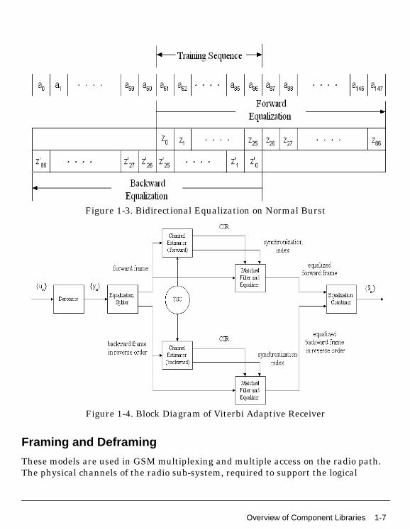
Figure 1-3. Bidirectional Equalization on Normal Burst
Figure 1-4. Block Diagram of Viterbi Adaptive Receiver
Framing and Deframing
These models are used in GSM multiplexing and multiple access on the radio path.The physical channels of the radio sub-system, required to support the logical
Overview of Component Libraries 1-7
GSM Design Library
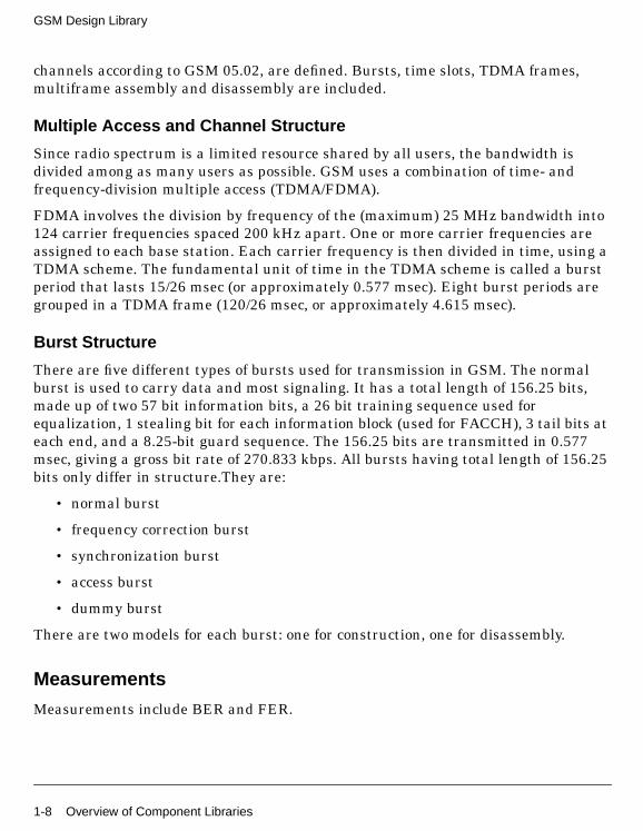
channels according to GSM 05.02, are defined. Bursts, time slots, TDMA frames,multiframe assembly and disassembly are included.
Multiple Access and Channel Structure
Since radio spectrum is a limited resource shared by all users, the bandwidth isdivided among as many users as possible. GSM uses a combination of time- andfrequency-division multiple access (TDMA/FDMA).
FDMA involves the division by frequency of the (maximum) 25 MHz bandwidth into124 carrier frequencies spaced 200 kHz apart. One or more carrier frequencies areassigned to each base station. Each carrier frequency is then divided in time, using aTDMA scheme. The fundamental unit of time in the TDMA scheme is called a burstperiod that lasts 15/26 msec (or approximately 0.577 msec). Eight burst periods aregrouped in a TDMA frame (120/26 msec, or approximately 4.615 msec).
Burst Structure
There are five different types of bursts used for transmission in GSM. The normalburst is used to carry data and most signaling. It has a total length of 156.25 bits,made up of two 57 bit information bits, a 26 bit training sequence used forequalization, 1 stealing bit for each information block (used for FACCH), 3 tail bits ateach end, and a 8.25-bit guard sequence. The 156.25 bits are transmitted in 0.577msec, giving a gross bit rate of 270.833 kbps. All bursts having total length of 156.25bits only differ in structure.They are:
• normal burst
• frequency correction burst
• synchronization burst
• access burst
• dummy burst
There are two models for each burst: one for construction, one for disassembly.
Measurements
Measurements include BER and FER.
1-8 Overview of Component Libraries
Modems
Implementation of modulation and demodulation of a GSM system is based on GSM05.04 and GSM 05.05.
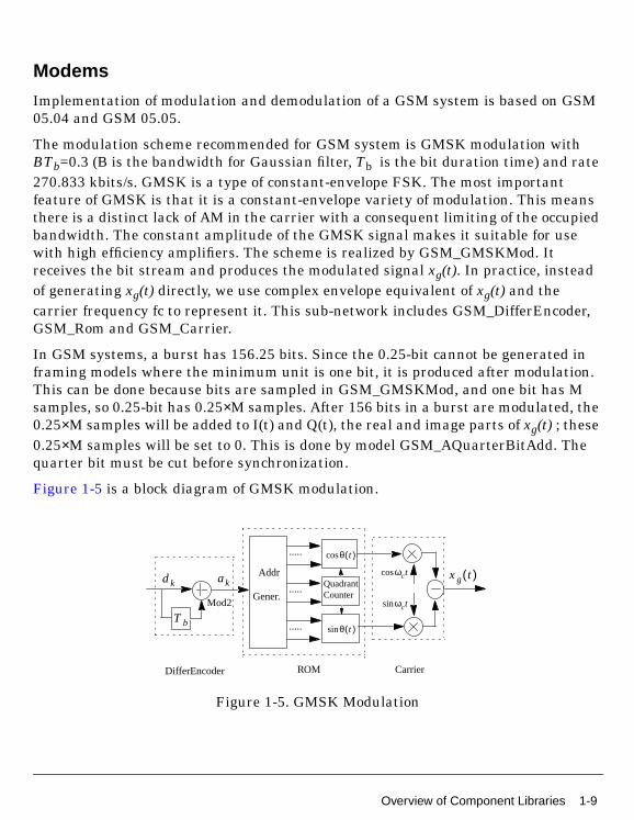
The modulation scheme recommended for GSM system is GMSK modulation withBTb=0.3 (B is the bandwidth for Gaussian filter, Tb is the bit duration time) and rate270.833 kbits/s. GMSK is a type of constant-envelope FSK. The most importantfeature of GMSK is that it is a constant-envelope variety of modulation. This meansthere is a distinct lack of AM in the carrier with a consequent limiting of the occupiedbandwidth. The constant amplitude of the GMSK signal makes it suitable for usewith high efficiency amplifiers. The scheme is realized by GSM_GMSKMod. Itreceives the bit stream and produces the modulated signal xg(t). In practice, insteadof generating xg(t) directly, we use complex envelope equivalent of xg(t) and thecarrier frequency fc to represent it. This sub-network includes GSM_DifferEncoder,GSM_Rom and GSM_Carrier.
In GSM systems, a burst has 156.25 bits. Since the 0.25-bit cannot be generated inframing models where the minimum unit is one bit, it is produced after modulation.This can be done because bits are sampled in GSM_GMSKMod, and one bit has Msamples, so 0.25-bit has 0.25×M samples. After 156 bits in a burst are modulated, the0.25×M samples will be added to I(t) and Q(t), the real and image parts of xg(t) ; these0.25×M samples will be set to 0. This is done by model GSM_AQuarterBitAdd. Thequarter bit must be cut before synchronization.
Figure 1-5 is a block diagram of GMSK modulation.
Figure 1-5. GMSK Modulation
Addr
.....
.....
.....
CounterQuadrant
Gener.Mod2
akdk
Tb
ωctcos
ωcsin t
θsin t( )
θ t( )cos
xg t( )
DifferEncoder ROM Carrier
Overview of Component Libraries 1-9
GSM Design Library
Speech Coding
The basic models are provided as required by ETSI GSM 06.10, in which the specifiedtranscoding procedure is applicable for the full-rate traffic channel (TCH) in GSMsystems. Users can build up the codec described in GSM specification or simulatetheir own speech codec algorithms used in telecommunication systems.
In GSM 06.10, the speech coding scheme called regular pulse excitation - long-termprediction - linear predictive coder (RPE-LTP) is specified. It describes the detailedmapping between input blocks of 160 speech samples in 13-bit uniform PCM formatto encoded blocks of 260 bits and from encoded blocks of 260 bits to output blocks of160 reconstructed speech samples. Basically, information from previous samples,which does not change quickly, is used to predict the current sample. Coefficients ofthe linear combination of the previous samples, plus an encoded form of the residual,the difference between the predicted and actual sample, represent the signal. Speechis divided into 20 msec samples, each of which is encoded as 260 bits, giving a totalbit rate of 13 kbps.
In GSM 06.10, an implementation of the RPE-LTP algorithm in fixed-pointarithmetic is provided using 16- and 32-bit integers. In GSM, the fixed-point class ofAgilent’s Advanced Design System is used.
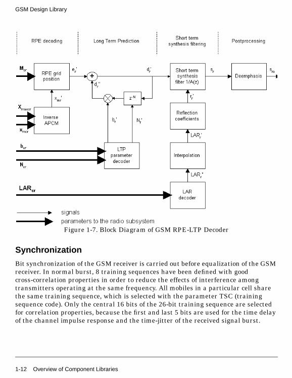
This speech coding scheme can be divided into several small basic signal processingmodels as illustrated in Figure 1-6 and Figure 1-7.
1-10 Overview of Component Libraries
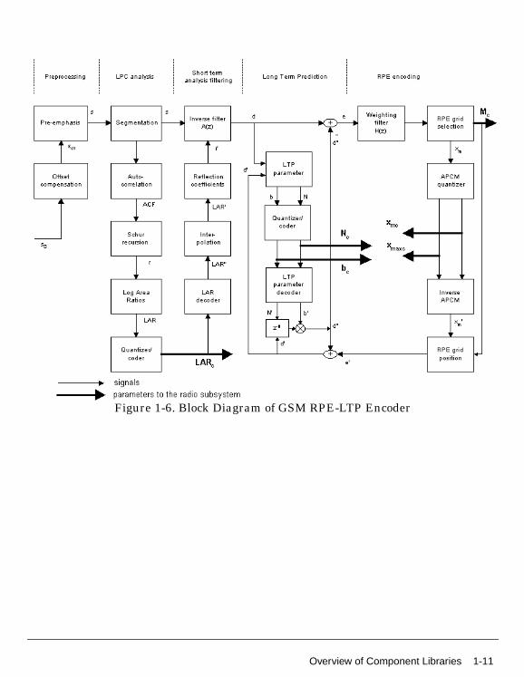
Figure 1-6. Block Diagram of GSM RPE-LTP Encoder
Overview of Component Libraries 1-11
GSM Design Library
Figure 1-7. Block Diagram of GSM RPE-LTP Decoder
Synchronization
Bit synchronization of the GSM receiver is carried out before equalization of the GSMreceiver. In normal burst, 8 training sequences have been defined with goodcross-correlation properties in order to reduce the effects of interference amongtransmitters operating at the same frequency. All mobiles in a particular cell sharethe same training sequence, which is selected with the parameter TSC (trainingsequence code). Only the central 16 bits of the 26-bit training sequence are selectedfor correlation properties, because the first and last 5 bits are used for the time delayof the channel impulse response and the time-jitter of the received signal burst.
1-12 Overview of Component Libraries

After symbol timing is implemented, one of the sample sequences made up of onesample per symbol will be determined, and the 0.25-bit from the 156.25 bits of oneburst will be cut. The output of this part will be 156 bits with one sample per symbol.
Figure 1-8 shows the implementation of GSM bit synchronization. The referencetraining sequence {Pk} can be GMSK modulated before phase recovery.
Figure 1-8. Implementation of the GSM Bit Synchronization
Glossary of Terms
Table 1-2. Glossary of TermsACPR adjacent channel power ratio
AWGN additive white Gaussian noise
BER bit error rate
bps bits per second
BSIC base station identity code
CIR channel impulse response
codec coder and decoder
CRC cyclic redundancy code
EVM error vector magnitude
SynchronizationModels
Glossary of Terms 1-13
GSM Design Library
References[1]D. M. Redl, An Introduction to GSM, Artech House Publishers, Boston
[2] European Telecommunications Standard Institute (ETSI), Rec. ETSI/GSM03.03, Numbering, addressing and identification, version 3.5.1, March 1992.
[3] European Telecommunications Standard Institute (ETSI), Rec. ETSI/GSM04.06, Mobile Station - Base Station System (MS - BSS) interface Data Link(DL) layer specification, version 3.5.1, March 1992.
FACCH fast associated control channel
FER frame error rate
GMSK gaussian minimum shift keying
GSM global system for mobile communications
ISI intersymbol interference
K constraint length
LAR log-area ratio
LPC linear predictive coding
LSB least significant bit
MLSE maximum-likelihood sequence estimation
MS mobile station
MSB most significant bit
NRZ non-return-to-zero
OQPSK offset quadrature phase shift keying
PLMN public land mobile network
QPSK quadrature phase shift keying
RACH random access channel
RPE-LTP regular pulse excitation long term prediction
SACCH slow associated control channel
SCH synchronization channel
SDCCH stand-alone dedicated control channel
SER symbol error rate
SINR signal-to-interference noise ratio
SIR signal-to-interference ratio
TCH/FS traffic channel/full-rate speech
Table 1-2. Glossary of Terms (continued)
1-14 References
[4] European Telecommunications Standard Institute (ETSI), Rec. ETSI/GSM05.01, Physical Layer on the Radio Path General Descriptions, version 3.5.1,March 1992.
[5] European Telecommunications Standard Institute (ETSI), Rec. ETSI/GSM05.02, Multiplexing and Multiple Access on the Radio Path, version 3.5.1, March1992.
[6] European Telecommunications Standard Institute (ETSI), Rec. ETSI/GSM05.03, Channel Coding, version 3.5.1, March 1992.
[7] European Telecommunications Standard Institute (ETSI), Rec. ETSI/GSM05.04, Modulation, version 3.5.1, March 1992.
[8] European Telecommunications Standard Institute (ETSI), Rec. ETSI/GSM05.05, Radio Transmission and Reception, version 3.5.1, March 1992.
[9] European Telecommunications Standard Institute (ETSI), Rec. ETSI/GSM05.10, Radio Subsystem Synchronization, version 3.5.1, March 1992.
[10] European Telecommunications Standard Institute (ETSI), Rec. ETSI/GSM06.01, Full Rate Speech Processing Functions, version 3.5.1,March 1992.
[11] European Telecommunications Standard Institute (ETSI), Rec. ETSI/GSM06.10, Full Rate Speech Transcoding, version 3.5.1, March 1992.
[12] S. Lin, D. J. Costello, JR., ERROR CONTROL CODING FundamentalsandApplications, Prentice Hall, Englewwood Cliffs, NJ, 1983
[13] J. E. Meggit, Error Correcting Codes and Their Implementation, IRE Trans. Inf.Theory, IT-7, October 1961, pp. 232-244.
[14] P. Q. Hua, L. W. Dong, H. Y. Hong, GSM System GMSK Modulator (in Chinese),Journal of Beijing University of Posts and Telecommunications, Vol.17, No.4,Dec., 1994, pp.20-25
[15] P. Q. Hua, G. Yong, L. W. Dong, Synchronization Design Theory OfDemodulation For Digital Land Mobile Radio System (in Chinese), Journal ofBeijing University of Posts and Telecommunications, Vol.18, No.2, Jun., 1995,pp.14-21
[16] G. D’Aria, L. Stola, and V. Zingarelli, Modeling and simulation of thepropagation characteristics of the 900MHz narrowband-TDMA CEPT/GSMmobile radio, in Proc. 39th IEEE Veh. Technol. Conf., San Francisco, CA, April29-May 3, 1989, pp. 631-639
References 1-15

GSM Design Library
[17] G. D’Aria, F. Muratore, Simulation and Performance of the Pan-European LandMobile Radio System, IEEE Trans. on Vehicular Technology, Vol. 41, No.2, May1992
[18] G. Ungerboeck, Adaptive maximum-likelihood receiver for carrier-modulateddata-transmission system, IEEE Trans. Commun., vol. COM-22, May 1974,pp.624-636.
[19] R. D’Avella, L. Moreno, M. Sant’Agostion, An adaptive MLSE receiver forTDMAdigital mobile radio, IEEE Jour. on SAC, vol. 7, NO. 1, Jan 1989, pp.122-129.
1-16 References
Chapter 2: Channel Coding Components
2-1
Channel Coding Components
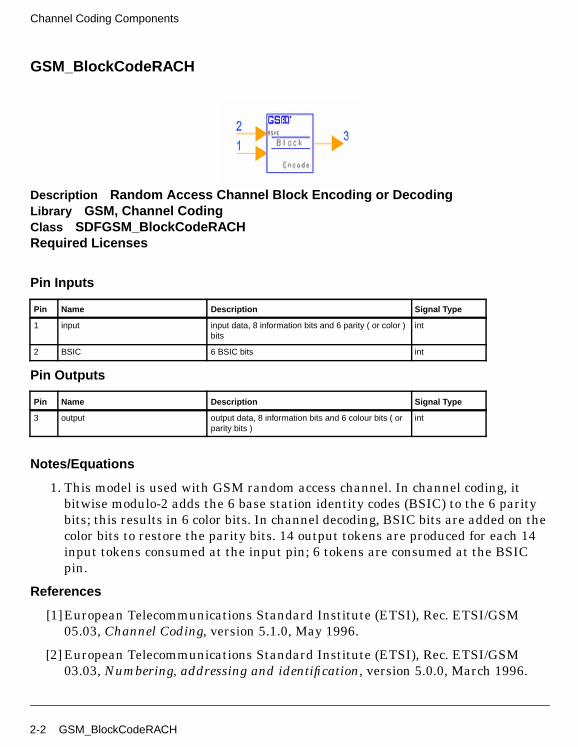
GSM_BlockCodeRACH
Description Random Access Channel Block Encoding or DecodingLibrary GSM, Channel CodingClass SDFGSM_BlockCodeRACHRequired Licenses
Pin Inputs
Pin Outputs
Notes/Equations
1. This model is used with GSM random access channel. In channel coding, itbitwise modulo-2 adds the 6 base station identity codes (BSIC) to the 6 paritybits; this results in 6 color bits. In channel decoding, BSIC bits are added on thecolor bits to restore the parity bits. 14 output tokens are produced for each 14input tokens consumed at the input pin; 6 tokens are consumed at the BSICpin.
References
[1]European Telecommunications Standard Institute (ETSI), Rec. ETSI/GSM05.03, Channel Coding, version 5.1.0, May 1996.
[2] European Telecommunications Standard Institute (ETSI), Rec. ETSI/GSM03.03, Numbering, addressing and identification, version 5.0.0, March 1996.
Pin Name Description Signal Type
1 input input data, 8 information bits and 6 parity ( or color )bits
int
2 BSIC 6 BSIC bits int
Pin Name Description Signal Type
3 output output data, 8 information bits and 6 colour bits ( orparity bits )
int
2-2 GSM_BlockCodeRACH
GSM_CC_WithTail
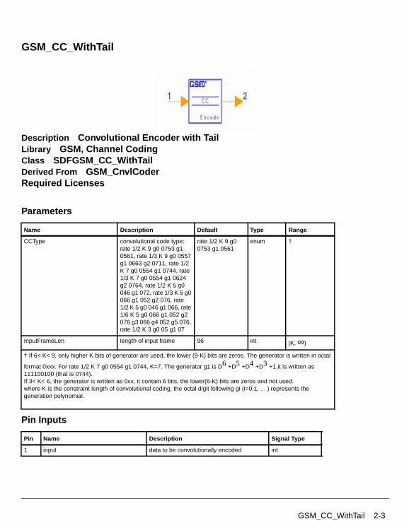
Description Convolutional Encoder with TailLibrary GSM, Channel CodingClass SDFGSM_CC_WithTailDerived From GSM_CnvlCoderRequired Licenses
Parameters
Pin Inputs
Name Description Default Type Range
CCType convolutional code type:rate 1/2 K 9 g0 0753 g10561, rate 1/3 K 9 g0 0557g1 0663 g2 0711, rate 1/2K 7 g0 0554 g1 0744, rate1/3 K 7 g0 0554 g1 0624g2 0764, rate 1/2 K 5 g0046 g1 072, rate 1/3 K 5 g0066 g1 052 g2 076, rate1/2 K 5 g0 046 g1 066, rate1/6 K 5 g0 066 g1 052 g2076 g3 066 g4 052 g5 076,rate 1/2 K 3 g0 05 g1 07
rate 1/2 K 9 g00753 g1 0561
enum †
InputFrameLen length of input frame 96 int [K,∞)
† If 6< K< 9, only higher K bits of generator are used, the lower (9-K) bits are zeros. The generator is written in octal
format 0xxx. For rate 1/2 K 7 g0 0554 g1 0744, K=7. The generator g1 is D6 +D5 +D4 +D3 +1,it is written as111100100 (that is 0744).If 3< K< 6, the generator is written as 0xx, it contain 6 bits, the lower(6-K) bits are zeros and not used.where K is the constraint length of convolutional coding, the octal digit following gi (i=0,1, ... ) represents thegeneration polynomial.
Pin Name Description Signal Type
1 input data to be convolutionally encoded int
GSM_CC_WithTail 2-3

Channel Coding Components
Pin Outputs
Notes/Equations
1. This model is used to convolutionally encode the input tailed frame.
InputFrameLen/rate (specified in CCType) output tokens are produced whenInputFrameLen input tokens are consumed.
References
[1]S. Lin and D. J. Costello, Jr., Error Control Coding Fundamentals andApplications, Prentice Hall, Englewood Cliffs NJ, 1983.
Pin Name Description Signal Type
2 output convolutionally encoded symbols int
2-4 GSM_CC_WithTail
GSM_Combiner
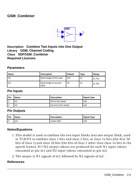
Description Combine Two Inputs into One OutputLibrary GSM, Channel CodingClass SDFGSM_CombinerRequired Licenses
Parameters
Pin Inputs
Pin Outputs
Notes/Equations
1. This model is used to combine the two input blocks into one output block, usedin TCH/FS to combine class 1 bits and class 2 bits, or class 1a bits (the first 50bits of class 1) and class 1b bits (the bits of class 1 other than class 1a bits in thespeech frame). N1+N2 output tokens are produced for each N1 input tokensconsumed at pin in1 and N2 input tokens consumed at pin in2.
2. The output is N1 signals of in1 followed by N2 signals of in2.
References
Name Description Default Type Range
N1 block length of first input 182 int (0,∞)
N2 block length of secondinput
78 int (0,∞)
Pin Name Description Signal Type
1 in1 first of two inputs real
2 in2 second of two inputs real
Pin Name Description Signal Type
3 out output data real
GSM_Combiner 2-5
Channel Coding Components
[1]European Telecommunications Standard Institute (ETSI), Rec. ETSI/GSM05.03, Channel Coding, version 5.1.0, May 1996.
2-6 GSM_Combiner
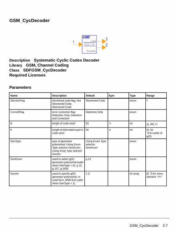
GSM_CycDecoder
Description Systematic Cyclic Codes DecoderLibrary GSM, Channel CodingClass SDFGSM_CycDecoderRequired Licenses
Parameters
Name Description Default Sym Type Range
ShortenFlag shortened code flag: NotShortened Code,Shortened Code
Shortened Code enum †
CorrectFlag error correction flag:Detection Only, Detectionand Correction
Detection Only enum
N length of code word 53 n int (0,∞) ††
K length of information part incode word
50 k int (0, N) N-K=order ofg(D)
GenType type of generatorpolynomial: Using EnumType selector GenEnum,Using Array Type selectorGenArr
Using Enum TypeselectorGenEnum
enum
GenEnum used to select g(D)generator polynomial (validwhen GenType = 0): g 13,g 157, g 2565
g 13 enum
GenArr used to specify g(D)generator polynomial, inoctal form, MSB first (validwhen GenType = 1)
1 3 int array [0, 7] for everyelement †††
GSM_CycDecoder 2-7
Channel Coding Components
Pin Inputs
Pin Outputs
Notes/Equations
1. This model is used to decode cyclically encoded data. K output tokens areproduced for each N input token consumed, where N is the length of the codeword and K is the length of the information in the code word.
2. Implementation
The Meggit decoder [1][2] is used. Figure 2-1 shows the cyclic codes decoderwith received polynomial r(D) is shifted into the syndrome register.
is the polynomial of received code word , i = 0, 1, ... , n−k, are the coefficientsof generator polynomial g(D),
The decoder is designed to correct one error (at most) in a code word
SS number of bits shortened ina code word (if this is ashortened cyclic code)
0 ss int (0,∞) †
† ShortenFlag is not used when CorrectFlag=Detection Only;SS is only used when CorrectFlag=Detection and Correction and ShortenFlag=Shortened Code†† The range of N should also satisfy:
(DN + 1) should be divisible by g(D) when ShortenFlag=Not Shortened Code and CorrectFlag=Detection and Correction, or
(D(N+SS) + 1) should be divisible by g(D) when ShortenFlag=Shortened Code and CorrectFlag=Detection and Correction, whereg(D) is the generator polynomial specified by GenEnum or GenArr.††† The last element of the array must be an odd number.
Pin Name Description Signal Type
1 input received code word int
Pin Name Description Signal Type
2 output decoded information block int
3 errMsg message indicating whether there is a error whichcannot be corrected
int
Name Description Default Sym Type Range
r D( ) r0Dn 1– r1Dn 2– … rn 2– D rn 1–+ + + +=
gi
g D( ) g0Dn k– g1Dn k– 1– … gn k– 1– D gn k–+ + + +=
2-8 GSM_CycDecoder

Figure 2-1. Cyclic Codes Decoder
References
[1]J. E. Meggit, Error Correcting Codes and Their Implementation, IRE Trans. Inf.Theory, IT-7, October 1961, pp. 232-244.
[2] S. Lin and D. J. Costello, Jr., Error Control Coding Fundamentals andApplications, Prentice Hall, Englewood Cliffs NJ, 1983.
GSM_CycDecoder 2-9

Channel Coding Components
GSM_CycEncoder
Description Systematic Cyclic Codes EncoderLibrary GSM, Channel CodingClass SDFGSM_CycEncoderRequired Licenses
Parameters
Pin Inputs
Name Description Default Sym Type Range
N length of code word 53 n int (0,∞) †
K length of information part incode word
50 k int (0, N) N-K=order ofg(D)
GenType type of generatorpolynomial selector: UsingEnum Type selectorGenEnum, Using ArrayType selector GenArr
Using Enum TypeselectorGenEnum
enum
GenEnum g(D) generator polynomial(valid when GenType = 0):g 13, g 157, g 2565, g45045, g 123, g20000440400011
g 13 enum
GenArr g(D) generator polynomial,in octal form, MSB first(valid when GenType = 1)
1 3 int array [0, 7] for everyelement ††
† (DN + 1) must be divisible by g(D) where g(D) is the generator polynomial specified by GenEnum or GenArr.
†† The last element in the array must be an odd number.
Pin Name Description Signal Type
1 input information block to be encoded int
2-10 GSM_CycEncoder
Pin Outputs
Notes/Equations
1. This model is used to encode input data into cyclic codes. N output tokens areproduced for each K tokens consumed.
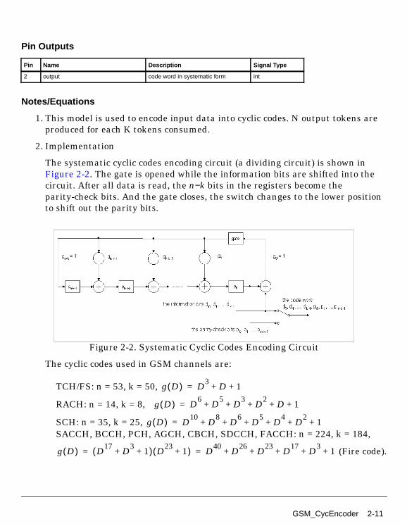
2. Implementation
The systematic cyclic codes encoding circuit (a dividing circuit) is shown inFigure 2-2. The gate is opened while the information bits are shifted into thecircuit. After all data is read, the n−k bits in the registers become theparity-check bits. And the gate closes, the switch changes to the lower positionto shift out the parity bits.
Figure 2-2. Systematic Cyclic Codes Encoding Circuit
The cyclic codes used in GSM channels are:
TCH/FS: n = 53, k = 50,
RACH: n = 14, k = 8,
SCH: n = 35, k = 25,SACCH, BCCH, PCH, AGCH, CBCH, SDCCH, FACCH: n = 224, k = 184,
(Fire code).
Pin Name Description Signal Type
2 output code word in systematic form int
g D( ) D3 D 1+ +=
g D( ) D6 D5 D3 D2 D 1+ + + + +=
g D( ) D10 D8 D6 D5 D4 D21+ + + + + +=
g D( ) D17 D31+ +( ) D23
1+( ) D40 D26 D23 D17 D31+ + + + += =
GSM_CycEncoder 2-11

Channel Coding Components
To agree with GSM05.03 (when divided by g(D) ), the code word yields aremainder equal to 1+D+D2+...+D(N-K-1). The parity-check bits is reversedbefore added at the end of information bits.
References
[1]S. Lin and D. J. Costello, Jr., Error Control Coding Fundamentals andApplications, Prentice Hall, Englewood Cliffs NJ, 1983.
[2] European Telecommunications Standard Institute (ETSI), Rec. ETSI/GSM05.03, Channel Coding, version 5.1.0, May 1996.
2-12 GSM_CycEncoder
GSM_DCC_WithTail
Description Viterbi Decoder for Convolutional Code with TailLibrary GSM, Channel CodingClass SDFGSM_DCC_WithTailDerived From GSM_ViterbiDecoderRequired Licenses
Parameters
Pin Inputs
Name Description Default Type Range
CCType convolutional code type:rate 1/2 K 9 g0 0753 g10561, rate 1/3 K 9 g0 0557g1 0663 g2 0711, rate 1/2K 7 g0 0554 g1 0744, rate1/3 K 7 g0 0554 g1 0624g2 0764, rate 1/2 K 5 g0046 g1 072, rate 1/3 K 5 g0066 g1 052 g2 076, rate1/2 K 5 g0 046 g1 066, rate1/6 K 5 g0 066 g1 052 g2076 g3 066 g4 052 g5 076,rate 1/2 K 3 g0 05 g1 07
rate 1/2 K 9 g00753 g1 0561
enum †
InputFrameLen input frame length 288 int [K+1,∞)
† If 6< K< 9, only higher K generator bits are used, the lower (9-K) bits are all zeros. The generator is written in octalformat 0xxx. For rate 1/2 K 7 g0 0554 g1 0744, K=7.Generator g1 is D6+D5+D4+D3+1, written as 111100100 (that is, 0744).If 3< K< 6, the generator is written as 0xx; it contain 6 bits, the lower(6-K)bits are zeros and is not used.where K is the constraint length of convolutional coding and gi (i=0,1, ... ) followed by an octal digit represents thegeneration polynomial.
Pin Name Description Signal Type
1 input the symbols to be decoded. real
GSM_DCC_WithTail 2-13
Channel Coding Components
Pin Outputs
Notes/Equations
1. This model is used to viterbi-decode convolutional code with tail.
InputFrameLen× rate (specified by CCType) output tokens are produced whenInputFrameLen input tokens are consumed.
References
[1]S. Lin and D. J. Costello, Jr., Error Control Coding Fundamentals andApplications, Prentice Hall, Englewood Cliffs NJ, 1983.
[2] R. Steele, Mobile Radio Communication, London: Pentech Press, 1992.
Pin Name Description Signal Type
2 output the decoded bits. int
2-14 GSM_DCC_WithTail
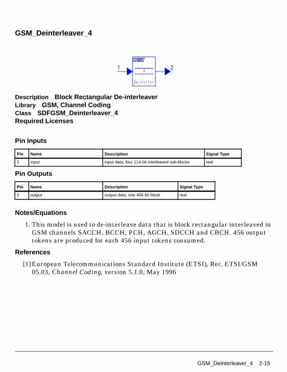
GSM_Deinterleaver_4
Description Block Rectangular De-interleaverLibrary GSM, Channel CodingClass SDFGSM_Deinterleaver_4Required Licenses
Pin Inputs
Pin Outputs
Notes/Equations
1. This model is used to de-interleave data that is block rectangular interleaved inGSM channels SACCH, BCCH, PCH, AGCH, SDCCH and CBCH. 456 outputtokens are produced for each 456 input tokens consumed.
References
[1]European Telecommunications Standard Institute (ETSI), Rec. ETSI/GSM05.03, Channel Coding, version 5.1.0, May 1996
Pin Name Description Signal Type
1 input input data, four 114-bit interleaved sub-blocks real
Pin Name Description Signal Type
2 output output data, one 456-bit block real
GSM_Deinterleaver_4 2-15
Channel Coding Components
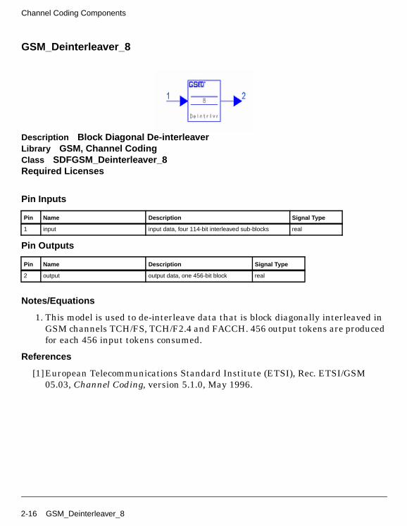
GSM_Deinterleaver_8
Description Block Diagonal De-interleaverLibrary GSM, Channel CodingClass SDFGSM_Deinterleaver_8Required Licenses
Pin Inputs
Pin Outputs
Notes/Equations
1. This model is used to de-interleave data that is block diagonally interleaved inGSM channels TCH/FS, TCH/F2.4 and FACCH. 456 output tokens are producedfor each 456 input tokens consumed.
References
[1]European Telecommunications Standard Institute (ETSI), Rec. ETSI/GSM05.03, Channel Coding, version 5.1.0, May 1996.
Pin Name Description Signal Type
1 input input data, four 114-bit interleaved sub-blocks real
Pin Name Description Signal Type
2 output output data, one 456-bit block real
2-16 GSM_Deinterleaver_8

GSM_Deinterleaver_F96
Description Diagonal De-interleaverLibrary GSM, Channel CodingClass SDFGSM_Deinterleaver_F96Required Licenses
Pin Inputs
Pin Outputs
Notes/Equations
1. This model is used to de-interleave data that is diagonally interleaved in GSMchannels TCH/F9.6, TCH/F4.8, TCH/H4.8, and TCH/H2.4. 114 output tokensare produced for each 114 input consumed.
References
[1]European Telecommunications Standard Institute (ETSI), Rec. ETSI/GSM05.03, Channel Coding, version 5.1.0, May 1996.
Pin Name Description Signal Type
1 input input data, 114-bit interleaved block real
Pin Name Description Signal Type
2 output output data, 114-bit data block real
GSM_Deinterleaver_F96 2-17

Channel Coding Components
GSM_Depuncture
Description Data DepunctureLibrary GSM, Channel CodingClass SDFGSM_DepunctureRequired Licenses
Pin Inputs
Pin Outputs
Notes/Equations
1. This model is used to insert zeros in the input symbols for implementing Viterbidecoding for punctured convolutional code in GSM data channel.
488 output tokens are produced when 456 input tokens consumed.
References
[1]European Telecommunications Standard Institute (ETSI), Rec. ETSI/GSM05.03, Channel Coding, version 5.1.0, May 1996
Pin Name Description Signal Type
1 input punctured convolutionlly encoded symbols real
Pin Name Description Signal Type
2 output depunctured convolutionally encoded symbols real
2-18 GSM_Depuncture
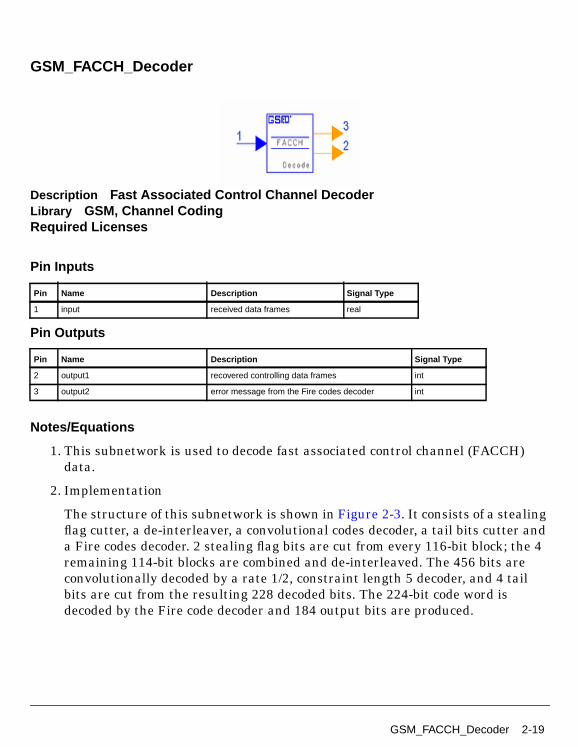
GSM_FACCH_Decoder
Description Fast Associated Control Channel DecoderLibrary GSM, Channel CodingRequired Licenses
Pin Inputs
Pin Outputs
Notes/Equations
1. This subnetwork is used to decode fast associated control channel (FACCH)data.
2. Implementation
The structure of this subnetwork is shown in Figure 2-3. It consists of a stealingflag cutter, a de-interleaver, a convolutional codes decoder, a tail bits cutter anda Fire codes decoder. 2 stealing flag bits are cut from every 116-bit block; the 4remaining 114-bit blocks are combined and de-interleaved. The 456 bits areconvolutionally decoded by a rate 1/2, constraint length 5 decoder, and 4 tailbits are cut from the resulting 228 decoded bits. The 224-bit code word isdecoded by the Fire code decoder and 184 output bits are produced.
Pin Name Description Signal Type
1 input received data frames real
Pin Name Description Signal Type
2 output1 recovered controlling data frames int
3 output2 error message from the Fire codes decoder int
GSM_FACCH_Decoder 2-19

Channel Coding Components
Figure 2-3. GSM_FACCH_Decoder Subnetwork
References
[1]European Telecommunications Standard Institute (ETSI), Rec. ETSI/GSM05.03, Channel Coding, version 5.1.0, May 1996.
2-20 GSM_FACCH_Decoder
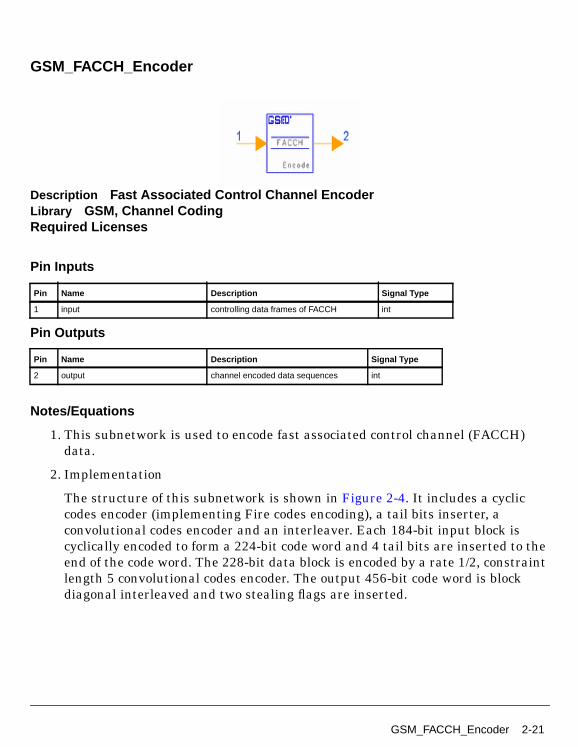
GSM_FACCH_Encoder
Description Fast Associated Control Channel EncoderLibrary GSM, Channel CodingRequired Licenses
Pin Inputs
Pin Outputs
Notes/Equations
1. This subnetwork is used to encode fast associated control channel (FACCH)data.
2. Implementation
The structure of this subnetwork is shown in Figure 2-4. It includes a cycliccodes encoder (implementing Fire codes encoding), a tail bits inserter, aconvolutional codes encoder and an interleaver. Each 184-bit input block iscyclically encoded to form a 224-bit code word and 4 tail bits are inserted to theend of the code word. The 228-bit data block is encoded by a rate 1/2, constraintlength 5 convolutional codes encoder. The output 456-bit code word is blockdiagonal interleaved and two stealing flags are inserted.
Pin Name Description Signal Type
1 input controlling data frames of FACCH int
Pin Name Description Signal Type
2 output channel encoded data sequences int
GSM_FACCH_Encoder 2-21

Channel Coding Components
Figure 2-4. GSM_FACCH_Encoder Subnetwork
References
[1]European Telecommunications Standard Institute (ETSI), Rec. ETSI/GSM05.03, Channel Coding, version 3.5.1, March 1992.
2-22 GSM_FACCH_Encoder
GSM_FireDecoder
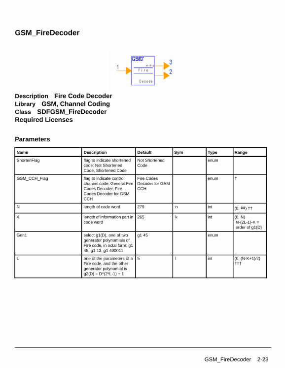
Description Fire Code DecoderLibrary GSM, Channel CodingClass SDFGSM_FireDecoderRequired Licenses
Parameters
Name Description Default Sym Type Range
ShortenFlag flag to indicate shortenedcode: Not ShortenedCode, Shortened Code
Not ShortenedCode
enum
GSM_CCH_Flag flag to indicate controlchannel code: General FireCodes Decoder, FireCodes Decoder for GSMCCH
Fire CodesDecoder for GSMCCH
enum †
N length of code word 279 n int (0,∞) ††
K length of information part incode word
265 k int (0, N) N-(2L-1)-K = order of g1(D)
Gen1 select g1(D), one of twogenerator polynomials ofFire code, in octal form: g145, g1 13, g1 400011
g1 45 enum
L one of the parameters of aFire code, and the othergenerator polynomial isg2(D) = D^(2*L-1) + 1
5 l int (0, (N-K+1)/2)†††
GSM_FireDecoder 2-23
Channel Coding Components
Pin Inputs
Pin Outputs
Notes/Equations
1. This model is used to decode Fire coded data. K output tokens are produced foreach N input token consumed.
References
[1]European Telecommunications Standard Institute (ETSI), Rec. ETSI/GSM05.03, Channel Coding, version 5.1.0, May 1996.
[2] S. Lin and D. J. Costello, Jr., Error Control Coding Fundamentals andApplications, Prentice Hall, Englewood Cliffs NJ, 1983.
SS number of bits shortened ina code word (used onlywhenShortenFlag=ShortenedCode)
0 ss int (0,∞)
† If GSM_CCH_Flag=Fire Codes Decoder for GSM CCH, all other parameters will not be used.†† N must also satisfy:
(DN +1) must be divisible by g(D) when ShortenFlag=Not Shortened Code, or
(D(N+SS) +1) must be divisible by g(D) when ShortenFlag=Shortened Code,
where g(D) is the generator polynomial generated by g1(D) and g2(D), and g1(D) is specified by Gen1, g2(D) = D(2L-1) +1.††† N+SS (when ShortenFlag=Shortened Code) orN (when ShortenFlag=Not Shortened Code)must equal LCM(2L-1, period), where period is the generator polynomial g1(D) period.
Pin Name Description Signal Type
1 input received code word int
Pin Name Description Signal Type
2 output decoded information block int
3 errMsg the message indicating error that cannot becorrected
int
Name Description Default Sym Type Range
2-24 GSM_FireDecoder
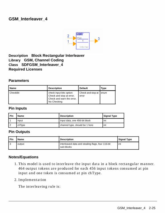
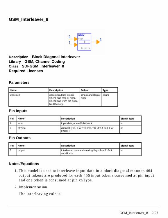
GSM_Interleaver_4
Description Block Rectangular InterleaverLibrary GSM, Channel CodingClass SDFGSM_Interleaver_4Required Licenses
Parameters
Pin Inputs
Pin Outputs
Notes/Equations
1. This model is used to interleave the input data in a block rectangular manner.464 output tokens are produced for each 456 input tokens consumed at pininput and one token is consumed at pin chType.
2. Implementation
The interleaving rule is:
Name Description Default Type
CheckBit check input bits option:Check and stop at error,Check and warn the error,No Checking
Check and stop aterror
enum
Pin Name Description Signal Type
1 input input data, one 456-bit block int
2 chType channel type, should be 1 here int
Pin Name Description Signal Type
3 output interleaved data and stealing flags, four 116-bitsub-blocks
int
GSM_Interleaver_4 2-25
Channel Coding Components
where c(n, k) is the kth bit in the nth 456-bit coded data block, N marks acertain data block, i(B, j) is the jth bit in the Bth 114-bit interleaved sub-block,and is the initial value of B.
The block of coded data is block rectangular interleaved, that is, a new datablock starts every 4th block and is distributed over 4 blocks.
Two stealing flags hu(B) and hl(B) are inserted into each block afterinterleaving. The flags should be equal to 1 here to indicate control channels.
In coding implementation, a preset table is used in converting the index k to theindex j.
References
[1]European Telecommunications Standard Institute (ETSI), Rec. ETSI/GSM05.03, Channel Coding, version 5.1.0, May 1996.
i B j,( ) c n k,( )= k 0 1 … 455n
, , ,0 1 … N N 1 …
B,+, , , ,
B0 4n k mod 4( )j
+ +2 49k( ) mod 57( ) k mod 8( ) div 4+
====
B0
2-26 GSM_Interleaver_4
GSM_Interleaver_8
Description Block Diagonal InterleaverLibrary GSM, Channel CodingClass SDFGSM_Interleaver_8Required Licenses
Parameters
Pin Inputs
Pin Outputs
Notes/Equations
1. This model is used to interleave input data in a block diagonal manner. 464output tokens are produced for each 456 input tokens consumed at pin inputand one token is consumed at pin chType.
2. Implementation
The interleaving rule is:
Name Description Default Type
CheckBit check input bits option:Check and stop at error,Check and warn the error,No Checking
Check and stop aterror
enum
Pin Name Description Signal Type
1 input input data, one 456-bit block int
2 chType channel type, 0 for TCH/FS, TCH/F2.4 and 1 forFACCH
int
Pin Name Description Signal Type
3 output interleaved data and stealing flags, four 116-bitsub-blocks
int
GSM_Interleaver_8 2-27
Channel Coding Components
where c(n, k) is the kth bit in the nth 456-bit coded data block, N marks acertain data block, i(B, j) is the jth bit in the Bth 114-bit interleaved sub-block,and is the initial value of B.
Stealing flags hu(B) and hl(B) are inserted into each block after interleaving;the flags are 0 for TCH/FS or TCH/F2.4 and 1 for FACCH.
In coding implementation, a preset table is used to convert index k to index j.
References
[1]European Telecommunications Standard Institute (ETSI), Rec. ETSI/GSM05.03, Channel Coding, version 5.1.0, May 1996.
i B j,( ) c n k,( )= k 0 1 … 455n
, , ,0 1 … N N 1 …
B,+, , , ,
B0 4n k mod 8( )j
+ +2 49k( ) mod 57( ) k mod 8( ) div 4+
====
B0
2-28 GSM_Interleaver_8
GSM_Interleaver_F96
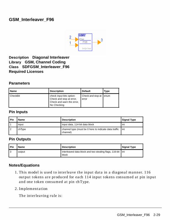
Description Diagonal InterleaverLibrary GSM, Channel CodingClass SDFGSM_Interleaver_F96Required Licenses
Parameters
Pin Inputs
Pin Outputs
Notes/Equations
1. This model is used to interleave the input data in a diagonal manner. 116output tokens are produced for each 114 input tokens consumed at pin inputand one token consumed at pin chType.
2. Implementation
The interleaving rule is:
Name Description Default Type
CheckBit check input bits option:Check and stop at error,Check and warn the error,No Checking
Check and stop aterror
enum
Pin Name Description Signal Type
1 input input data, 114-bit data block int
2 chType channel type (must be 0 here to indicate data trafficchannel)
int
Pin Name Description Signal Type
3 output interleaved data block and two stealing flags, 116-bitblock
int
GSM_Interleaver_F96 2-29
Channel Coding Components
where c(n, k) is the kth bit in the nth 456-bit coded data block, N marks acertain data block, i(B, j) is the jth bit in the Bth 114-bit interleaved sub-block,and is the initial value of B.
By dividing the 456-bit data block into four 114-bit blocks, we can change therule to
where is the index of the new blocks.
Stealing flags hu(B) and hl(B) are inserted into each block after interleaving.The flags must be 0 to indicate traffic channels. In coding implementation, apreset table is used in converting index k to index j.The interleaver output willhave a 114×19 token delay.
References
[1]European Telecommunications Standard Institute (ETSI), Rec. ETSI/GSM05.03, Channel Coding, version 5.1.0, May 1996.
i B j,( ) c n k,( )= k 0 1 … 455n
, , ,0 1 … N N 1 …
B,+, , , ,
B0 4n k mod 19( ) k div 114( )j
+ + +k mod 19 19 k mod 6( )+
====
B0
i B j,( ) c n' k,( )= k 0 1 … 113n'
, , ,0 1 … N N 1 …
B,+, , , ,
B0 n' k mod 19( )j
+ +k mod 19 19 k mod 6( )+
====
n' 4n k div 114( )+=
2-30 GSM_Interleaver_F96
GSM_InverseReord
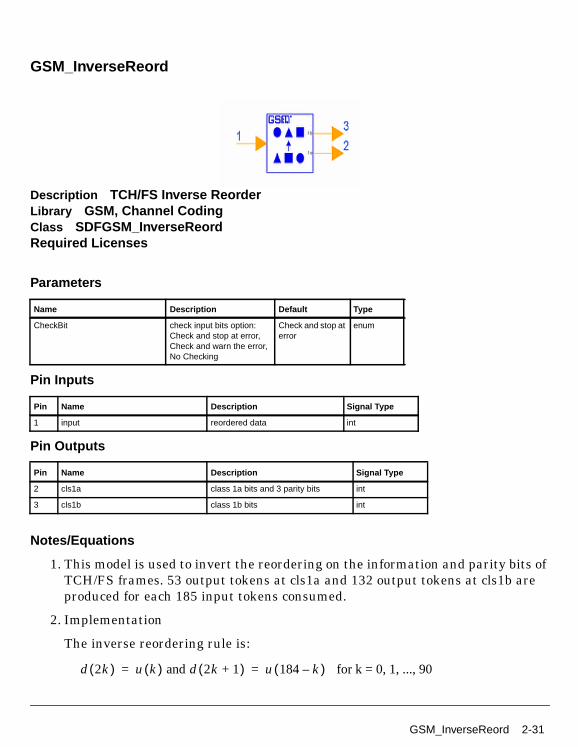
Description TCH/FS Inverse ReorderLibrary GSM, Channel CodingClass SDFGSM_InverseReordRequired Licenses
Parameters
Pin Inputs
Pin Outputs
Notes/Equations
1. This model is used to invert the reordering on the information and parity bits ofTCH/FS frames. 53 output tokens at cls1a and 132 output tokens at cls1b areproduced for each 185 input tokens consumed.
2. Implementation
The inverse reordering rule is:
Name Description Default Type
CheckBit check input bits option:Check and stop at error,Check and warn the error,No Checking
Check and stop aterror
enum
Pin Name Description Signal Type
1 input reordered data int
Pin Name Description Signal Type
2 cls1a class 1a bits and 3 parity bits int
3 cls1b class 1b bits int
d 2k( ) u k( ) and d 2k 1+( ) u 184 k–( ) for k = 0, 1, ..., 90= =
GSM_InverseReord 2-31
Channel Coding Components
where d(k), k = 0, 1, ... , 181 are the bits of class 1, p(k), k = 0, 1, 2 are the paritybits of the class 1a bits, and u(k), k = 0, 1, ... , 184 are the reordered bits.
References
[1]European Telecommunications Standard Institute (ETSI), Rec. ETSI/GSM05.03, Channel Coding, version 5.1.0, May 1996.
p k( ) u 91 k+( ) for k = 0, 1, 2=
2-32 GSM_InverseReord

GSM_Puncture
Description Data PunctureLibrary GSM, Channel CodingClass SDFGSM_PunctureRequired Licenses
Pin Inputs
Pin Outputs
Notes/Equations
1. This model is used to puncture the input stream to implement puncturedconvolutional code for GSM data channel.
456 output tokens are produced when 488 input tokens consumed.
References
[1]European Telecommunications Standard Institute (ETSI), Rec. ETSI/GSM05.03, Channel Coding, version 5.1.0, May 1996.
Pin Name Description Signal Type
1 input convolutionally encoded symbols. int
Pin Name Description Signal Type
2 output punctured Convolutionally encoded symbols. int
GSM_Puncture 2-33

Channel Coding Components
GSM_RACH_Decoder
Description Random Access Channel DecoderLibrary GSM, Channel CodingRequired Licenses
Pin Inputs
Pin Outputs
Notes/Equations
1. This subnetwork is used to decode random access channel data.
2. Implementation
The structure of this subnetwork is shown in Figure 2-5. It consists of aconvolutional codes decoder, a tail bits cutter, base station identity codes (BSIC)adder, and a cyclic codes decoder. The input 36-bit block is convolutionallydecoded by a rate 1/2, constraint length 5 decoder, and 4 tail bits are cut fromthe resulting 18 bits. In the remaining 14 bits, there are 6 color bits that aremasked with the 6 BSIC bits to produce 6 parity check bits. These parity checkbits and the other 8 information bits are cyclically decoded and 8 output bits areproduced.
Pin Name Description Signal Type
1 input1 received data frames real
2 input2 base station identity codes int
Pin Name Description Signal Type
3 output1 recovered controlling data frames int
4 output2 error message from the Fire codes decoder int
2-34 GSM_RACH_Decoder
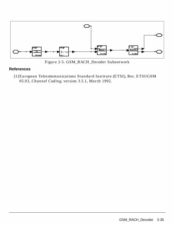
Figure 2-5. GSM_RACH_Decoder Subnetwork
References
[1]European Telecommunications Standard Institute (ETSI), Rec. ETSI/GSM05.03, Channel Coding, version 3.5.1, March 1992.
GSM_RACH_Decoder 2-35
Channel Coding Components
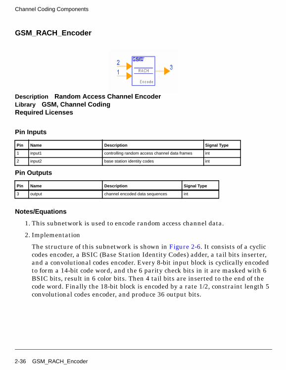
GSM_RACH_Encoder
Description Random Access Channel EncoderLibrary GSM, Channel CodingRequired Licenses
Pin Inputs
Pin Outputs
Notes/Equations
1. This subnetwork is used to encode random access channel data.
2. Implementation
The structure of this subnetwork is shown in Figure 2-6. It consists of a cycliccodes encoder, a BSIC (Base Station Identity Codes) adder, a tail bits inserter,and a convolutional codes encoder. Every 8-bit input block is cyclically encodedto form a 14-bit code word, and the 6 parity check bits in it are masked with 6BSIC bits, result in 6 color bits. Then 4 tail bits are inserted to the end of thecode word. Finally the 18-bit block is encoded by a rate 1/2, constraint length 5convolutional codes encoder, and produce 36 output bits.
Pin Name Description Signal Type
1 input1 controlling random access channel data frames int
2 input2 base station identity codes int
Pin Name Description Signal Type
3 output channel encoded data sequences int
2-36 GSM_RACH_Encoder
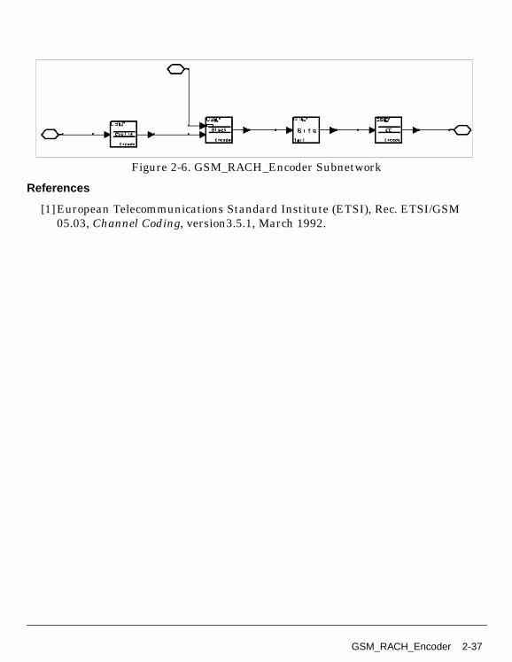
Figure 2-6. GSM_RACH_Encoder Subnetwork
References
[1]European Telecommunications Standard Institute (ETSI), Rec. ETSI/GSM05.03, Channel Coding, version3.5.1, March 1992.
GSM_RACH_Encoder 2-37
Channel Coding Components
GSM_Reorder
Description TCH/FS ReorderLibrary GSM, Channel CodingClass SDFGSM_ReorderRequired Licenses
Parameters
Pin Inputs
Pin Outputs
Notes/Equations
1. This model is used to reorder the information and parity bits of TCH/FS frames.185 output tokens are produced, 53 input tokens are consumed at the cls1a pinand 132 input tokens are consumed at the cls1b pin.
2. Implementation
The reordering rule is:
Name Description Default Type
CheckBit check input bits option:Check and stop at error,Check and warn the error,No Checking
Check and stop aterror
enum
Pin Name Description Signal Type
1 cls1a cyclic encoded class 1a bits and 3 parity bits int
2 cls1b class 1b bits int
Pin Name Description Signal Type
3 out reordered data int
u k( ) d 2k( ) and u 184 k–( ) d 2k 1+( ) for k = 0, 1, ..., 90= =
2-38 GSM_Reorder
where d(k), k=0, 1, ... , 181 are the bits of class 1, p(k), k=0, 1, 2 are the paritybits of the class 1a bits, and u (k), k=0, 1, ... , 184 are the reordered bits.
References
[1]European Telecommunications Standard Institute (ETSI), Rec. ETSI/GSM05.03, Channel Coding, version 5.1.0, May 1996.
u 91 k+( ) p k( ) for k = 0, 1, 2=
GSM_Reorder 2-39

Channel Coding Components
GSM_RmvStlFlgs
Description Remove Stealing FlagsLibrary GSM, Channel CodingClass SDFGSM_RmvStlFlgsRequired Licenses
Pin Inputs
Pin Outputs
Notes/Equations
1. This model removes the two stealing flags from the burst before de-interleaving.144 output, 1 hl and 1 hu tokens are produced for each 116 input tokensconsumed.
2. Implementation
Upper layer models will select an appropriate de-interleaving scheme using thestealing flags. The stealing flags are hl(B) and hu(B), where B is the index of thedata block. Assume d(B, k), B = 0, 1, ... , k = 0, 1, ... , 115, are the bits in block B,then hl(B) = d(B, 57) and hu(B) = d(B, 58).
References
Pin Name Description Signal Type
1 input 116-bit data block of normal burst real
Pin Name Description Signal Type
2 output 114-bit information block without stealing flags real
3 hl stealing flag hl(B) = e(B,57): odd-numbered bits inthe 114-bit block
real
4 hu stealing flag hu(B) = e(B,58): even numbered bits inthe 114-bit block
real
2-40 GSM_RmvStlFlgs

[1]European Telecommunications Standard Institute (ETSI), Rec. ETSI/GSM05.03, Channel Coding, version 5.1.0, May 1996.
GSM_RmvStlFlgs 2-41
Channel Coding Components
GSM_SACCH_Decoder
Description Slow Associated Control Channel DecoderLibrary GSM, Channel CodingRequired Licenses
Pin Inputs
Pin Outputs
Notes/Equations
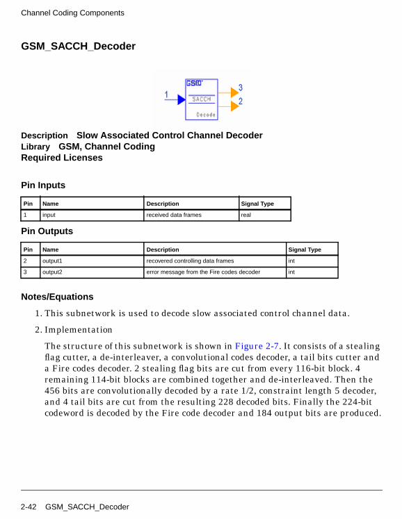
1. This subnetwork is used to decode slow associated control channel data.
2. Implementation
The structure of this subnetwork is shown in Figure 2-7. It consists of a stealingflag cutter, a de-interleaver, a convolutional codes decoder, a tail bits cutter anda Fire codes decoder. 2 stealing flag bits are cut from every 116-bit block. 4remaining 114-bit blocks are combined together and de-interleaved. Then the456 bits are convolutionally decoded by a rate 1/2, constraint length 5 decoder,and 4 tail bits are cut from the resulting 228 decoded bits. Finally the 224-bitcodeword is decoded by the Fire code decoder and 184 output bits are produced.
Pin Name Description Signal Type
1 input received data frames real
Pin Name Description Signal Type
2 output1 recovered controlling data frames int
3 output2 error message from the Fire codes decoder int
2-42 GSM_SACCH_Decoder
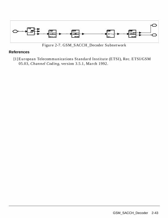
Figure 2-7. GSM_SACCH_Decoder Subnetwork
References
[1]European Telecommunications Standard Institute (ETSI), Rec. ETSI/GSM05.03, Channel Coding, version 3.5.1, March 1992.
GSM_SACCH_Decoder 2-43
Channel Coding Components
GSM_SACCH_Encoder
Description Slow Associated Control Channel EncoderLibrary GSM, Channel CodingRequired Licenses
Pin Inputs
Pin Outputs
Notes/Equations
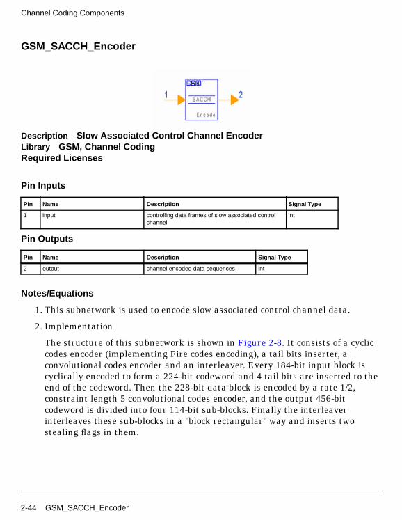
1. This subnetwork is used to encode slow associated control channel data.
2. Implementation
The structure of this subnetwork is shown in Figure 2-8. It consists of a cycliccodes encoder (implementing Fire codes encoding), a tail bits inserter, aconvolutional codes encoder and an interleaver. Every 184-bit input block iscyclically encoded to form a 224-bit codeword and 4 tail bits are inserted to theend of the codeword. Then the 228-bit data block is encoded by a rate 1/2,constraint length 5 convolutional codes encoder, and the output 456-bitcodeword is divided into four 114-bit sub-blocks. Finally the interleaverinterleaves these sub-blocks in a "block rectangular" way and inserts twostealing flags in them.
Pin Name Description Signal Type
1 input controlling data frames of slow associated controlchannel
int
Pin Name Description Signal Type
2 output channel encoded data sequences int
2-44 GSM_SACCH_Encoder
Figure 2-8. GSM_SACCH_Encoder Subnetwork
References
[1]European Telecommunications Standard Institute (ETSI), Rec. ETSI/GSM05.03, Channel Coding, version 3.5.1, March 1992.
GSM_SACCH_Encoder 2-45
Channel Coding Components
GSM_SCH_Decoder
Description Synchronization Channel DecoderLibrary GSM, Channel CodingRequired Licenses
Pin Inputs
Pin Outputs
Notes/Equations
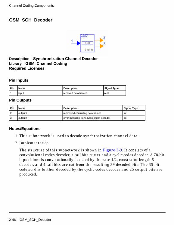
1. This subnetwork is used to decode synchronization channel data.
2. Implementation
The structure of this subnetwork is shown in Figure 2-9. It consists of aconvolutional codes decoder, a tail bits cutter and a cyclic codes decoder. A 78-bitinput block is convolutionally decoded by the rate 1/2, constraint length 5decoder, and 4 tail bits are cut from the resulting 39 decoded bits. The 35-bitcodeword is further decoded by the cyclic codes decoder and 25 output bits areproduced.
Pin Name Description Signal Type
1 input received data frames real
Pin Name Description Signal Type
2 output1 recovered controlling data frames int
3 output2 error message from cyclic codes decoder int
2-46 GSM_SCH_Decoder
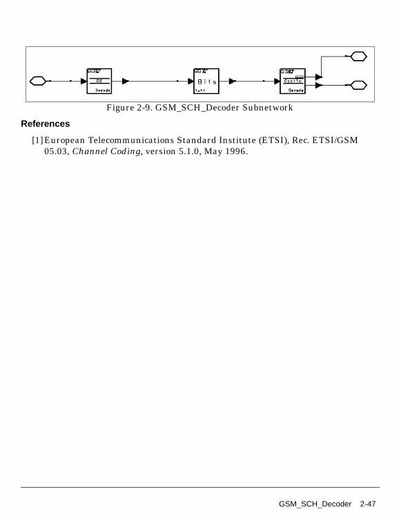
Figure 2-9. GSM_SCH_Decoder Subnetwork
References
[1]European Telecommunications Standard Institute (ETSI), Rec. ETSI/GSM05.03, Channel Coding, version 5.1.0, May 1996.
GSM_SCH_Decoder 2-47
Channel Coding Components
GSM_SCH_Encoder
Description Synchronization Channel EncoderLibrary GSM, Channel CodingRequired Licenses
Pin Inputs
Pin Outputs
Notes/Equations
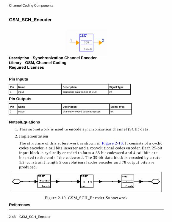
1. This subnetwork is used to encode synchronization channel (SCH) data.
2. Implementation
The structure of this subnetwork is shown in Figure 2-10. It consists of a cycliccodes encoder, a tail bits inserter and a convolutional codes encoder. Each 25-bitinput block is cyclically encoded to form a 35-bit codeword and 4 tail bits areinserted to the end of the codeword. The 39-bit data block is encoded by a rate1/2, constraint length 5 convolutional codes encoder and 78 output bits areproduced.
Figure 2-10. GSM_SCH_Encoder Subnetwork
References
Pin Name Description Signal Type
1 input controlling data frames of SCH int
Pin Name Description Signal Type
2 output channel encoded data sequences int
2-48 GSM_SCH_Encoder

[1]European Telecommunications Standard Institute (ETSI), Rec. ETSI/GSM05.03, Channel Coding, version 5.1.0, May 1996.
GSM_SCH_Encoder 2-49
Channel Coding Components
GSM_Splitter
Description Split Input Block into Two Output BlocksLibrary GSM, Channel CodingClass SDFGSM_SplitterRequired Licenses
Parameters
Pin Inputs
Pin Outputs
Notes/Equations
1. This model is used to split the input block into two output blocks. It is used inTCH/FS to separate class 1 and class 2 bits, or class 1a bits (the first 50 bits ofclass 1) and class 1b bits (the bits of class 1 other than class 1a bits in thespeech frame). Each firing, N1 output tokens at out1 and N2 tokens at out2 areproduced for each N1+N2 input tokens consumed.
References
Name Description Default Type Range
N1 block length of first output 182 int (0,∞)
N2 block length of secondoutput
78 int (0,∞)
Pin Name Description Signal Type
1 in input data real
Pin Name Description Signal Type
2 out1 first of two outputs real
3 out2 second of two outputs real
2-50 GSM_Splitter

[1]European Telecommunications Standard Institute (ETSI), Rec. ETSI/GSM05.03, Channel Coding, version 5.1.0, May 1996.
GSM_Splitter 2-51

Channel Coding Components
GSM_TailBits
Description Add or Remove Tailing BitsLibrary GSM, Channel CodingClass SDFGSM_TailBitsRequired Licenses
Parameters
Pin Inputs
Pin Outputs
Notes/Equations
1. This model is used to add tailing bits to or remove tailing bits from the inputframes.
Name Description Default Type Range
AddRmvSwitch tailing bits option: Adding,Removing
Adding enum
CheckBit check input bits option:Check and stop at error,Check and warn the error,No Checking
Check and stop aterror
enum
N number of tailing bits in aframe
4 int (0,∞)
InfoLen number of information bitsin a frame
185 int (0,∞)
Pin Name Description Signal Type
1 input input frame int
Pin Name Description Signal Type
2 output output frame int
2-52 GSM_TailBits

N+InfoLen output tokens are produced for each InfoLen input token consumedwhen AddRmvSwitch=Adding; InfoLen output tokens are produced for eachN+InfoLen input token consumed when AddRmvSwitch=Removing.
2. Implementation
When AddRmvSwitch=Adding, N tailing bits are added after each InfoLeninformation bits; when AddRmvSwitch=Removing, N tailing bits are removedfrom each N+InfoLen input bits.
References
[1]European Telecommunications Standard Institute (ETSI), Rec. ETSI/GSM05.03, Channel Coding, version 5.1.0, May 1996.
GSM_TailBits 2-53
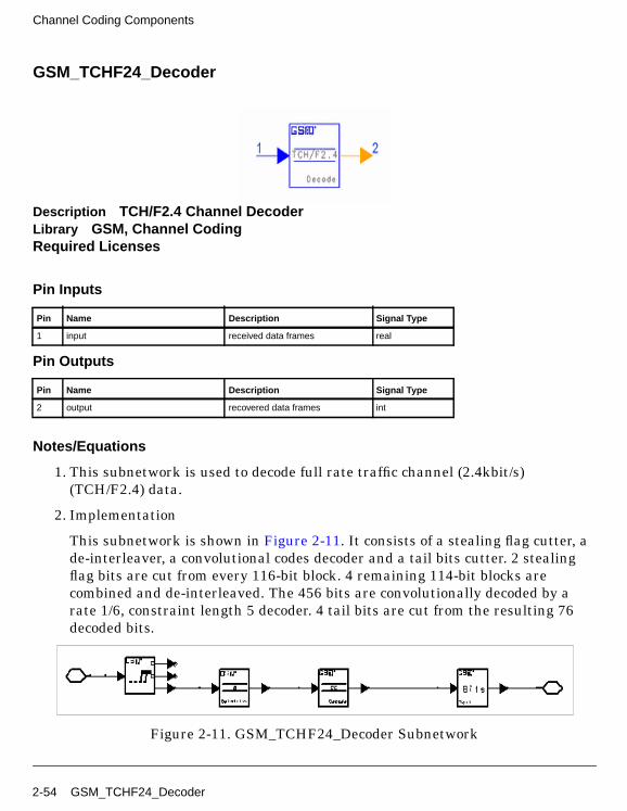
Channel Coding Components
GSM_TCHF24_Decoder
Description TCH/F2.4 Channel DecoderLibrary GSM, Channel CodingRequired Licenses
Pin Inputs
Pin Outputs
Notes/Equations
1. This subnetwork is used to decode full rate traffic channel (2.4kbit/s)(TCH/F2.4) data.
2. Implementation
This subnetwork is shown in Figure 2-11. It consists of a stealing flag cutter, ade-interleaver, a convolutional codes decoder and a tail bits cutter. 2 stealingflag bits are cut from every 116-bit block. 4 remaining 114-bit blocks arecombined and de-interleaved. The 456 bits are convolutionally decoded by arate 1/6, constraint length 5 decoder. 4 tail bits are cut from the resulting 76decoded bits.
Figure 2-11. GSM_TCHF24_Decoder Subnetwork
Pin Name Description Signal Type
1 input received data frames real
Pin Name Description Signal Type
2 output recovered data frames int
2-54 GSM_TCHF24_Decoder
References
[1]European Telecommunications Standard Institute (ETSI), Rec. ETSI/GSM05.03, Channel Coding, version 5.1.0, May 1996.
GSM_TCHF24_Decoder 2-55

Channel Coding Components
GSM_TCHF24_Encoder
Description TCH/F2.4 Channel EncoderLibrary GSM, Channel CodingRequired Licenses
Pin Inputs
Pin Outputs
Notes/Equations
1. This subnetwork is used to encode full rate traffic channel (2.4 kbit/s)(TCH/F2.4) data.
2. Implementation
This subnetwork is shown in Figure 2-12. It consists of a tail bits inserter, aconvolutional codes encoder, and an interleaver. Four tail bits are inserted intoeach 72 input information bits. These 76 bits are convolutionally coded in rate1/6, constraint length 5 encoder and interleaved in a block diagonal manner.
Pin Name Description Signal Type
1 input data frames of TCH/F2.4 int
Pin Name Description Signal Type
2 output channel encoded data sequences int
2-56 GSM_TCHF24_Encoder

Figure 2-12. GSM_TCHF24_Encoder Subnetwork
References
[1]European Telecommunications Standard Institute (ETSI), Rec. ETSI/GSM05.03, Channel Coding, version 5.1.0, May 1996.
GSM_TCHF24_Encoder 2-57

Channel Coding Components
GSM_TCHF48_Decoder
Description TCH/F4.8 Channel DecoderLibrary GSM, Channel CodingRequired Licenses
Pin Inputs
Pin Outputs
Notes/Equations
1. This subnetwork is used to decode full rate traffic channel (4.8kbit/s)(TCH/F4.8) data.
2. Implementation
The subnetwork structure is shown in Figure 2-13. It consists of a stealing flagcutter, a de-interleaver, a convolutional codes decoder, and a tail bits cutter.
Two stealing flag bits are cut from each 116-bit block; the remaining 114-bitblock is de-interleaved in a diagonal manner. A delay of 228 bits is inserted tokeep the bit index consistent. Four 114-bit de-interleaved blocks are combinedand convolutionally decoded by a rate 1/3, constraint length 5 decoder. Four tailbits are cut from each 19 bits.
Pin Name Description Signal Type
1 input received data frames real
Pin Name Description Signal Type
2 output recovered data frames int
2-58 GSM_TCHF48_Decoder
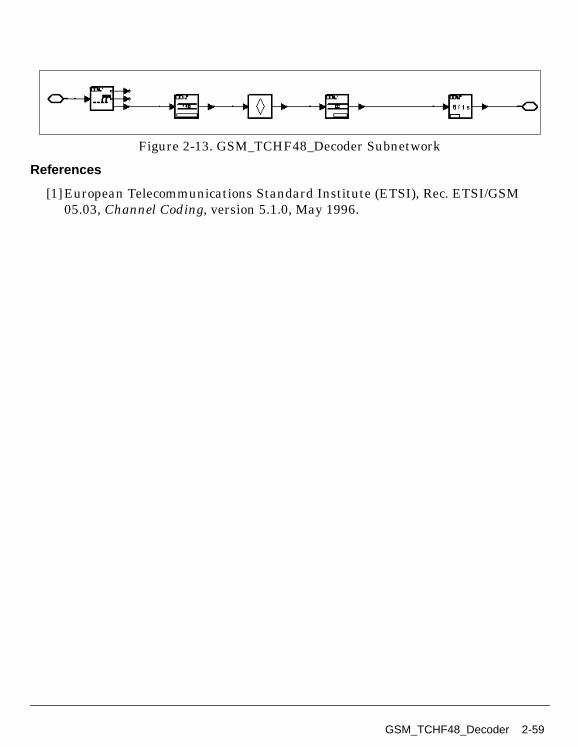
Figure 2-13. GSM_TCHF48_Decoder Subnetwork
References
[1]European Telecommunications Standard Institute (ETSI), Rec. ETSI/GSM05.03, Channel Coding, version 5.1.0, May 1996.
GSM_TCHF48_Decoder 2-59
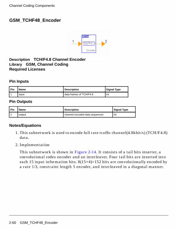
Channel Coding Components
GSM_TCHF48_Encoder
Description TCH/F4.8 Channel EncoderLibrary GSM, Channel CodingRequired Licenses
Pin Inputs
Pin Outputs
Notes/Equations
1. This subnetwork is used to encode full rate traffic channel(4.8kbit/s) (TCH/F4.8)data.
2. Implementation
This subnetwork is shown in Figure 2-14. It consists of a tail bits inserter, aconvolutional codes encoder and an interleaver. Four tail bits are inserted intoeach 15 input information bits. 8(15+4)=152 bits are convolutionally encoded bya rate 1/3, constraint length 5 encoder, and interleaved in a diagonal manner.
Pin Name Description Signal Type
1 input data frames of TCH/F4.8 int
Pin Name Description Signal Type
2 output channel encoded data sequences int
2-60 GSM_TCHF48_Encoder
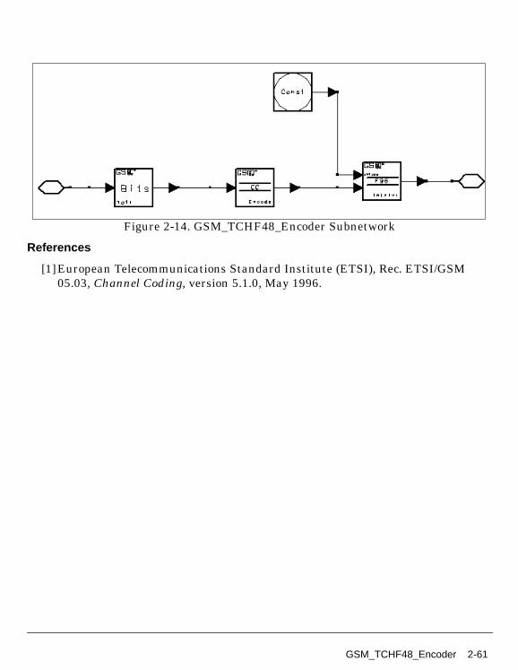
Figure 2-14. GSM_TCHF48_Encoder Subnetwork
References
[1]European Telecommunications Standard Institute (ETSI), Rec. ETSI/GSM05.03, Channel Coding, version 5.1.0, May 1996.
GSM_TCHF48_Encoder 2-61
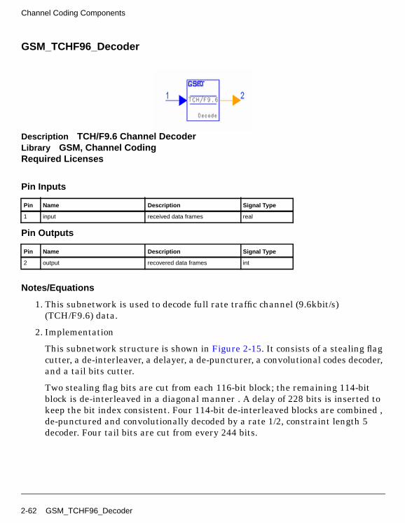
Channel Coding Components
GSM_TCHF96_Decoder
Description TCH/F9.6 Channel DecoderLibrary GSM, Channel CodingRequired Licenses
Pin Inputs
Pin Outputs
Notes/Equations
1. This subnetwork is used to decode full rate traffic channel (9.6kbit/s)(TCH/F9.6) data.
2. Implementation
This subnetwork structure is shown in Figure 2-15. It consists of a stealing flagcutter, a de-interleaver, a delayer, a de-puncturer, a convolutional codes decoder,and a tail bits cutter.
Two stealing flag bits are cut from each 116-bit block; the remaining 114-bitblock is de-interleaved in a diagonal manner . A delay of 228 bits is inserted tokeep the bit index consistent. Four 114-bit de-interleaved blocks are combined ,de-punctured and convolutionally decoded by a rate 1/2, constraint length 5decoder. Four tail bits are cut from every 244 bits.
Pin Name Description Signal Type
1 input received data frames real
Pin Name Description Signal Type
2 output recovered data frames int
2-62 GSM_TCHF96_Decoder
Figure 2-15. GSM_TCHF96_Decoder Subnetwork
References
[1]European Telecommunications Standard Institute (ETSI), Rec. ETSI/GSM05.03, Channel Coding, version 5.1.0, May 1996.
GSM_TCHF96_Decoder 2-63
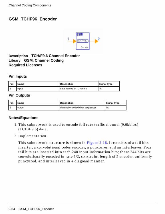
Channel Coding Components
GSM_TCHF96_Encoder
Description TCH/F9.6 Channel EncoderLibrary GSM, Channel CodingRequired Licenses
Pin Inputs
Pin Outputs
Notes/Equations
1. This subnetwork is used to encode full rate traffic channel (9.6kbit/s)(TCH/F9.6) data.
2. Implementation
This subnetwork structure is shown in Figure 2-16. It consists of a tail bitsinserter, a convolutional codes encoder, a puncturer, and an interleaver. Fourtail bits are inserted into each 240 input information bits; these 244 bits areconvolutionally encoded in rate 1/2, constraint length of 5 encoder, uniformlypunctured, and interleaved in a diagonal manner.
Pin Name Description Signal Type
1 input data frames of TCH/F9.6 int
Pin Name Description Signal Type
2 output channel encoded data sequences int
2-64 GSM_TCHF96_Encoder
Figure 2-16. GSM_TCHF96_Encoder Subnetwork
References
[1]European Telecommunications Standard Institute (ETSI), Rec. ETSI/GSM05.03, Channel Coding, version 5.1.0, May 1996.
GSM_TCHF96_Encoder 2-65
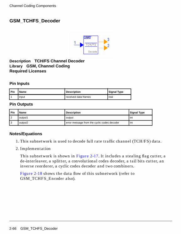
Channel Coding Components
GSM_TCHFS_Decoder
Description TCH/FS Channel DecoderLibrary GSM, Channel CodingRequired Licenses
Pin Inputs
Pin Outputs
Notes/Equations
1. This subnetwork is used to decode full rate traffic channel (TCH/FS) data.
2. Implementation
This subnetwork is shown in Figure 2-17. It includes a stealing flag cutter, ade-interleaver, a splitter, a convolutional codes decoder, a tail bits cutter, aninverse reorderer, a cyclic codes decoder and two combiners.
Figure 2-18 shows the data flow of this subnetwork (refer toGSM_TCHFS_Encoder also).
Pin Name Description Signal Type
1 input received data frames real
Pin Name Description Signal Type
2 output1 output int
3 output2 error message from the cyclic codes decoder int
2-66 GSM_TCHFS_Decoder
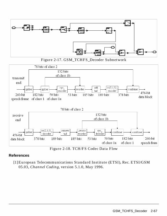
.
Figure 2-17. GSM_TCHFS_Decoder Subnetwork
Figure 2-18. TCH/FS Codec Data Flow
References
[1]European Telecommunications Standard Institute (ETSI), Rec. ETSI/GSM05.03, Channel Coding, version 5.1.0, May 1996.
GSM_TCHFS_Decoder 2-67
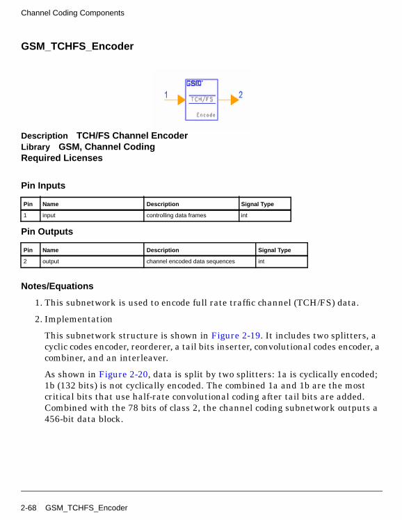
Channel Coding Components
GSM_TCHFS_Encoder
Description TCH/FS Channel EncoderLibrary GSM, Channel CodingRequired Licenses
Pin Inputs
Pin Outputs
Notes/Equations
1. This subnetwork is used to encode full rate traffic channel (TCH/FS) data.
2. Implementation
This subnetwork structure is shown in Figure 2-19. It includes two splitters, acyclic codes encoder, reorderer, a tail bits inserter, convolutional codes encoder, acombiner, and an interleaver.
As shown in Figure 2-20, data is split by two splitters: 1a is cyclically encoded;1b (132 bits) is not cyclically encoded. The combined 1a and 1b are the mostcritical bits that use half-rate convolutional coding after tail bits are added.Combined with the 78 bits of class 2, the channel coding subnetwork outputs a456-bit data block.
Pin Name Description Signal Type
1 input controlling data frames int
Pin Name Description Signal Type
2 output channel encoded data sequences int
2-68 GSM_TCHFS_Encoder
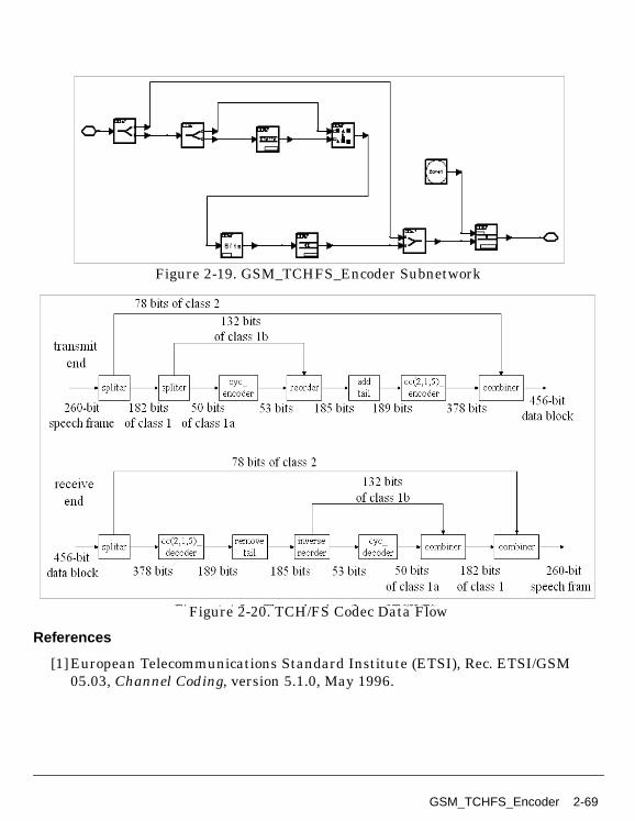
Figure 2-19. GSM_TCHFS_Encoder Subnetwork
Figure 2-20. TCH/FS Codec Data Flow
References
[1]European Telecommunications Standard Institute (ETSI), Rec. ETSI/GSM05.03, Channel Coding, version 5.1.0, May 1996.
GSM_TCHFS_Encoder 2-69
Channel Coding Components
2-70 GSM_TCHFS_Encoder

Chapter 3: Equalization Components
3-1

Equalization Components
GSM_ChannelEstimator
Description Channel Estimator Used in GSM Channel EqualizationLibrary GSM, EqualizationClass SDFGSM_ChannelEstimatorRequired Licenses
Parameters
Pin Inputs
Pin Outputs
Notes/Equations
Name Description Default Type Range
Direction direction of estimation:Forward, Backward
Forward enum
BurstType burst type: Normal Burst,Synchronization Burst,Access Burst
Normal Burst enum
L maximum delay of channel,in bit duration units, Tb
5 int [1, MAX_L] †
† MAX_L, typically ≤ 5, is defined in EquHeader.h
Pin Name Description Signal Type
1 input synchronized and derotated data complex
2 tsc training sequence code, defined by GSM 05.02 int
Pin Name Description Signal Type
3 output estimate of complex channel impluse response complex
4 index index used to correct synchronization int
3-2 GSM_ChannelEstimator
1. This model is used to estimate the impulse response of the equivalent channel,which includes the effect of modulation and derotation. L+1 output tokens areproduced at pin output and one token is produced at pin index for each N inputtokens consumed at pin input and one token consumed at pin tsc, where N isframe length (see Table 3-1) .
References
[1]R. Steele, Mobile Radio Communications, London: Pentech Press, 1992.
[2] European Telecommunications Standard Institute (ETSI), Rec. ETSI/GSM05.02, Multiplexing and Multiple Access on the Radio Path, version 4.8.0, Nov.1996.
Table 3-1. Frame Length N Value
N BurstType
87 + 2 × L Normal Burst
106 + 2 × L Synchronization Burst
80 + 2 × L Access Burst
GSM_ChannelEstimator 3-3
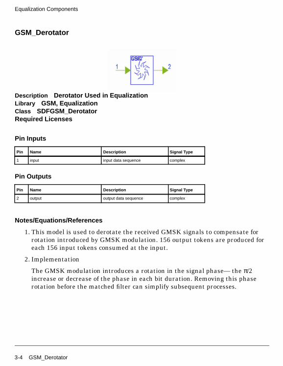
Equalization Components
GSM_Derotator
Description Derotator Used in EqualizationLibrary GSM, EqualizationClass SDFGSM_DerotatorRequired Licenses
Pin Inputs
Pin Outputs
Notes/Equations/References
1. This model is used to derotate the received GMSK signals to compensate forrotation introduced by GMSK modulation. 156 output tokens are produced foreach 156 input tokens consumed at the input.
2. Implementation
The GMSK modulation introduces a rotation in the signal phase— the π/2increase or decrease of the phase in each bit duration. Removing this phaserotation before the matched filter can simplify subsequent processes.
Pin Name Description Signal Type
1 input input data sequence complex
Pin Name Description Signal Type
2 output output data sequence complex
3-4 GSM_Derotator
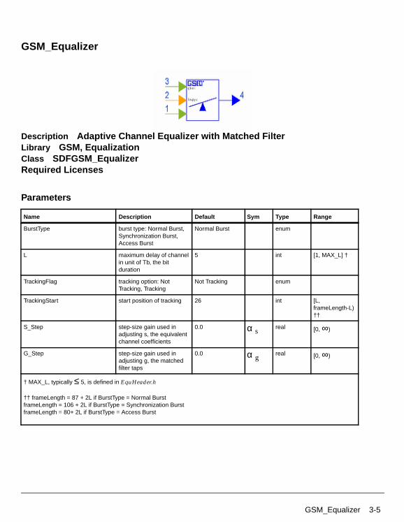
GSM_Equalizer
Description Adaptive Channel Equalizer with Matched FilterLibrary GSM, EqualizationClass SDFGSM_EqualizerRequired Licenses
Parameters
Name Description Default Sym Type Range
BurstType burst type: Normal Burst,Synchronization Burst,Access Burst
Normal Burst enum
L maximum delay of channelin unit of Tb, the bitduration
5 int [1, MAX_L] †
TrackingFlag tracking option: NotTracking, Tracking
Not Tracking enum
TrackingStart start position of tracking 26 int [L,frameLength-L)††
S_Step step-size gain used inadjusting s, the equivalentchannel coefficients
0.0 α sreal [0,∞)
G_Step step-size gain used inadjusting g, the matchedfilter taps
0.0 α greal [0,∞)
† MAX_L, typically ≤ 5, is defined in EquHeader.h
†† frameLength = 87 + 2L if BurstType = Normal BurstframeLength = 106 + 2L if BurstType = Synchronization BurstframeLength = 80+ 2L if BurstType = Access Burst
GSM_Equalizer 3-5
Equalization Components
Pin Inputs
Pin Outputs
Notes/Equations
1. This model is used to adaptively equalize received data. N output tokens areproduced at pin output for each N input token consumed at pin input, L+1 inputtokens consumed at pin chnl and one token consumed at pin index, where N isframe length (see Table 3-2).
2. Implementation
This model includes a matched filter and a Viterbi processor.
The matched filter is used before the Viterbi processor to establish an optimumsignal-to-noise ratio. The number of taps of the matched filter is (L+1). Intraining mode, the matched filter gets its tap coefficients fromGSM_ChannelEstimator, which are the complex conjugates of the reversesequence of the estimated channel impulse response coefficients. In trackingmode, the matched filter establishes an optimum signal-to-noise ratio of itsoutput signals, while adjusting its tap gains adaptively by a gradient algorithm.
The Viterbi processor uses a modified Viterbi algorithm [1] that operatesdirectly on the matched filter output without whitening the noise.
Pin Name Description Signal Type
1 input derotated signal, one sample per bit complex
2 index index used to correct synchronization int
3 chnl estimate of complex channel complex
Pin Name Description Signal Type
4 output equalized data real
Table 3-2. Frame Length N Value
N BurstType
87 + 2 × L Normal Burst
106 + 2 × L Synchronization Burst
80 + 2 × L Access Burst
3-6 GSM_Equalizer
If TrackingFlag is set to Tracking, the entire sequence is equalized withouttracking, then equalized again using the tracking algorithm and the results ofthe first equalization. From this, the tracking performance band can beobtained.
The index input is used on the results of the Viterbi processor to further correctthe synchronization. The results are output from the offset of the value of indexand zeros are added to the end.
References
[1]G. Ungerboeck, Adaptive maximum-likelihood receiver for carrier-modulateddata-transmission system, IEEE Trans. Commun., vol. COM-22, pp. 624-636,May 1974.
[2] R. D’Avella, L. Moreno, M. Sant’Agostion, An adaptive MLSE receiver forTDMA digital mobile radio, IEEE Jour. on SAC, vol. 7, No. 1, pp. 122-129, Jan1989.
[3] P. Qinhua, G. Yong, L. Weidong, Synchronization design theory of demodulationfor digital land mobile radio system, Jour. of Beijing University of Posts andTelecommunications, vol. 18, No. 2, pp. 14-21, Jun 1995.
GSM_Equalizer 3-7
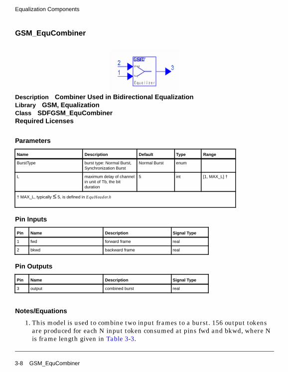
Equalization Components
GSM_EquCombiner
Description Combiner Used in Bidirectional EqualizationLibrary GSM, EqualizationClass SDFGSM_EquCombinerRequired Licenses
Parameters
Pin Inputs
Pin Outputs
Notes/Equations
1. This model is used to combine two input frames to a burst. 156 output tokensare produced for each N input token consumed at pins fwd and bkwd, where Nis frame length given in Table 3-3.
Name Description Default Type Range
BurstType burst type: Normal Burst,Synchronization Burst
Normal Burst enum
L maximum delay of channelin unit of Tb, the bitduration
5 int [1, MAX_L] †
† MAX_L, typically ≤ 5, is defined in EquHeader.h
Pin Name Description Signal Type
1 fwd forward frame real
2 bkwd backward frame real
Pin Name Description Signal Type
3 output combined burst real
3-8 GSM_EquCombiner

2. Implementation
Two input frames are combined to form a burst. Figure 3-1 shows the split of anormal burst. Implementation of the synchronization burst is the same exceptfor the length of training sequence, which is 64 bits.
The forward frame starts from the beginning of the training sequence and endsat the end of the burst; the backward frame starts from the end of the trainingsequence and ends at the beginning of the burst. Since both frames contain atraining sequence, only one of the training sequences (Figure 3-1 shows theforward frame) is embedded in the resulting burst. 8 bits of 0 are added to theend as guard bits to form a normal burst.
Figure 3-1. Bidirectional Equalization for Normal Burst
References
[1]European Telecommunications Standard Institute (ETSI), Rec. ETSI/GSM05.02, Multiplexing and Multiple Access on the Radio Path, version 4.8.0, Nov.1996.
Table 3-3. Value of frame length N
N BurstType
87 + 2 × L Normal Burst
106 + 2 × L Synchronization Burst
GSM_EquCombiner 3-9
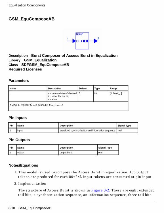
Equalization Components
GSM_EquComposeAB
Description Burst Composer of Access Burst in EqualizationLibrary GSM, EqualizationClass SDFGSM_EquComposeABRequired Licenses
Parameters
Pin Inputs
Pin Outputs
Notes/Equations
1. This model is used to compose the Access Burst in equalization. 156 outputtokens are produced for each 80+2×L input tokens are consumed at pin input.
2. Implementation
The structure of Access Burst is shown in Figure 3-2. There are eight extendedtail bits, a synchronization sequence, an information sequence, three tail bits
Name Description Default Type Range
L maximum delay of channelin unit of Tb, the bitduration
5 int [1, MAX_L] †
† MAX_L, typically ≤ 5, is defined in EquHeader.h
Pin Name Description Signal Type
1 input equalized synchronizaiton and information sequence real
Pin Name Description Signal Type
2 output output burst real
3-10 GSM_EquComposeAB
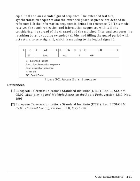
equal to 0 and an extended guard sequence. The extended tail bits,synchronization sequence and the extended guard sequence are defined inreference [1]; the information sequence is defined in reference [2]. This modelreceives the synchronization and information sequences with tail bitsconsidering the spread of the channel and the matched filter, and composes theresulting burst by adding extended tail bits and filling the guard period withnot return to zero signal 1, which is mapping to the logical signal 0.
Figure 3-2. Access Burst Structure
References
[1]European Telecommunications Standard Institute (ETSI), Rec. ETSI/GSM05.02, Multiplexing and Multiple Access on the Radio Path, version 4.8.0, Nov.1996.
[2] European Telecommunications Standard Institute (ETSI), Rec. ETSI/GSM05.03, Channel Coding, version 5.1.0, May 1996.
ET Sync. Info. T GP
8 41 36 3 68
ET: Extended Tail bits
Sync.: Synchronization sequence
Info.: Information sequence
T: Tail bits
GP: Guard Period
GSM_EquComposeAB 3-11

Equalization Components
GSM_EquDecomposeAB
Description Burst Decomposer of Access Burst in EqualizationLibrary GSM, EqualizationClass SDFGSM_EquDecomposeABRequired Licenses
Parameters
Pin Inputs
Pin Outputs
Notes/Equations
1. This model is used to decompose the Access Burst in equalization. 80+2×Loutput tokens are produced for each 156 input tokens consumed at pin input.
2. Implementation
The structure of Access Burst is shown as Figure 3-3. There are eight extendedtail bits, a synchronization sequence, an information sequence, three tail bits
Name Description Default Type Range
L maximum delay of channelin unit of Tb, the bitduration
5 int [1, MAX_L] †
† MAX_L, typically ≤ 5, is defined in EquHeader.h
Pin Name Description Signal Type
1 input input burst complex
Pin Name Description Signal Type
2 output output synchronization and information sequence complex
3-12 GSM_EquDecomposeAB
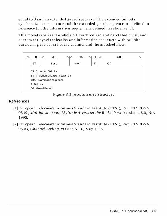
equal to 0 and an extended guard sequence. The extended tail bits,synchronization sequence and the extended guard sequence are defined inreference [1]; the information sequence is defined in reference [2].
This model receives the whole bit synchronized and derotated burst, andoutputs the synchronization and information sequences with tail bitsconsidering the spread of the channel and the matched filter.
Figure 3-3. Access Burst Structure
References
[1]European Telecommunications Standard Institute (ETSI), Rec. ETSI/GSM05.02, Multiplexing and Multiple Access on the Radio Path, version 4.8.0, Nov.1996.
[2] European Telecommunications Standard Institute (ETSI), Rec. ETSI/GSM05.03, Channel Coding, version 5.1.0, May 1996.
ET Sync. Info. T GP
8 41 36 3 68
ET: Extended Tail bits
Sync.: Synchronization sequence
Info.: Information sequence
T: Tail bits
GP: Guard Period
GSM_EquDecomposeAB 3-13
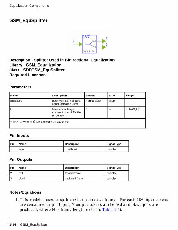
Equalization Components
GSM_EquSplitter
Description Splitter Used in Bidirectional EqualizationLibrary GSM, EqualizationClass SDFGSM_EquSplitterRequired Licenses
Parameters
Pin Inputs
Pin Outputs
Notes/Equations
1. This model is used to split one burst into two frames. For each 156 input tokensare consumed at pin input, N output tokens at the fwd and bkwd pins areproduced, where N is frame length (refer to Table 3-4).
Name Description Default Type Range
BurstType burst type: Normal Burst,Synchronization Burst
Normal Burst enum
L Mmaximum delay ofchannel in unit of Tb, thebit duration
5 int [1, MAX_L] †
† MAX_L, typically ≤ 5, is defined in EquHeader.h
Pin Name Description Signal Type
1 input input burst complex
Pin Name Description Signal Type
2 fwd forward frame complex
3 bkwd backward frame complex
3-14 GSM_EquSplitter
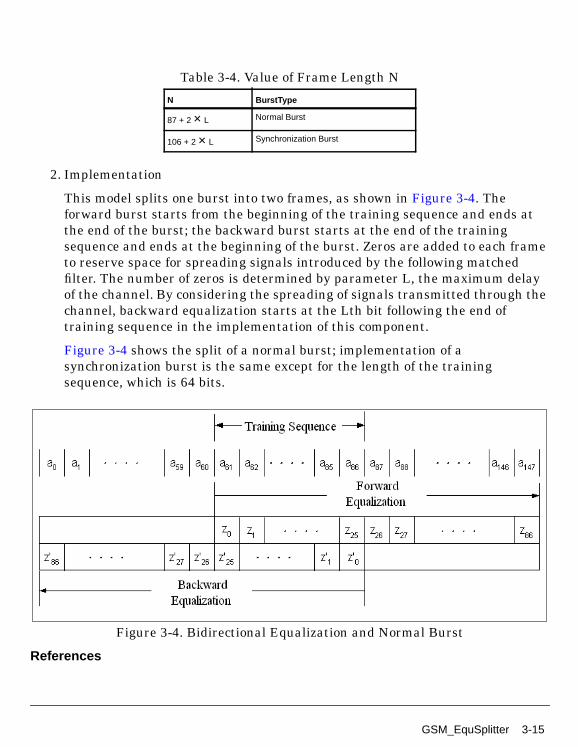
2. Implementation
This model splits one burst into two frames, as shown in Figure 3-4. Theforward burst starts from the beginning of the training sequence and ends atthe end of the burst; the backward burst starts at the end of the trainingsequence and ends at the beginning of the burst. Zeros are added to each frameto reserve space for spreading signals introduced by the following matchedfilter. The number of zeros is determined by parameter L, the maximum delayof the channel. By considering the spreading of signals transmitted through thechannel, backward equalization starts at the Lth bit following the end oftraining sequence in the implementation of this component.
Figure 3-4 shows the split of a normal burst; implementation of asynchronization burst is the same except for the length of the trainingsequence, which is 64 bits.
Figure 3-4. Bidirectional Equalization and Normal Burst
References
Table 3-4. Value of Frame Length N
N BurstType
87 + 2 × L Normal Burst
106 + 2 × L Synchronization Burst
GSM_EquSplitter 3-15
Equalization Components
[1]European Telecommunications Standard Institute (ETSI), Rec. ETSI/GSM05.02, Multiplexing and Multiple Access on the Radio Path, version 4.8.0, Nov.1996.
3-16 GSM_EquSplitter
GSM_Filter
Description 7-Pole Butterworth FilterLibrary GSM, EqualizationRequired Licenses
Pin Inputs
Pin Outputs
Notes/Equations
1. This subnetwork is a 7-pole butterworth filter that is used as a baseband filterin the GSM receiver.
2. Implementation
This subnetwork is designed by Digital Filter Designer of Agilent’s AdvancedDesign System. The 3db bandwidth is 100 kHz.
Figure 3-5 shows the subnetwork structure.
Pin Name Description Signal Type
1 input modulated signal that has passed through thechannel
real
Pin Name Description Signal Type
2 output filtered baseband signal real
GSM_Filter 3-17

Equalization Components
Figure 3-5. GSM_Filter Subnetwork
References
[1]S. M. Redl, Matthias, M. W. Oliphant, An Introduction To GSM, Artech HousePublishers, 1995.
3-18 GSM_Filter
GSM_Receiver
Description Adaptive MLSE ReceiverLibrary GSM, EqualizationRequired Licenses
Parameters
Pin Inputs
Name Description Default Sym Type Range
TSC training sequence code 0 int [0, 7]
BurstType burst type: Normal Burst,Synchronization Burst
Normal Burst enum
L maximum delay of channelin unit of Tb, the bitduration
5 int [1, MAX_L] †
TrackingFlag tracking option: NotTracking, Tracking
Not Tracking enum
TrackingStart start position of tracking 26 int [L,frameLength-L)††
S_Step step-size gain used inadjusting s, the equivalentchannel coefficients
0.0 α sreal [0,∞)
G_Step step-size gain used inadjusting g, the matchedfilter taps
0.0 α greal [0,∞)
† MAX_L, typically ≤ 5, is defined in EquHeader.h
†† if BurstType=Normal Burst, frameLength=87+2L if BurstType=Synchronization Burst, frameLength=106+2L.
Pin Name Description Signal Type
1 input input data sequence complex
GSM_Receiver 3-19
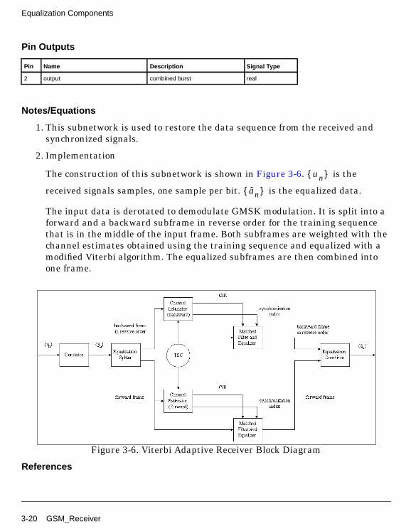
Equalization Components
Pin Outputs
Notes/Equations
1. This subnetwork is used to restore the data sequence from the received andsynchronized signals.
2. Implementation
The construction of this subnetwork is shown in Figure 3-6. is the
received signals samples, one sample per bit. is the equalized data.
The input data is derotated to demodulate GMSK modulation. It is split into aforward and a backward subframe in reverse order for the training sequencethat is in the middle of the input frame. Both subframes are weighted with thechannel estimates obtained using the training sequence and equalized with amodified Viterbi algorithm. The equalized subframes are then combined intoone frame.
Figure 3-6. Viterbi Adaptive Receiver Block Diagram
References
Pin Name Description Signal Type
2 output combined burst real
un{ }
an{ }
3-20 GSM_Receiver
[1]European Telecommunications Standard Institute (ETSI), Rec. ETSI/GSM05.03, Channel Coding, version 5.1.0, May 1996.
[2] R. Steele, Mobile Radio Communications, London: Pentech Press, 1992.
[3] European Telecommunications Standard Institute (ETSI), Rec. ETSI/GSM05.02, Multiplexing and Multiple Access on the Radio Path, version 4.8.0, Nov.1996.
[4] G. Ungerboeck, Adaptive maximum-likelihood receiver for carrier-modulateddata-transmission system, IEEE Trans. Commun., vol. COM-22, May 1974, pp.624-636.
[5] R. D’Avella, L. Moreno, M. Sant’Agostion, An adaptive MLSE receiver forTDMA digital mobile radio, IEEE J. Select. Areas Commun., vol. 7, Jan. 1989,pp. 122-129 .
GSM_Receiver 3-21

Equalization Components
GSM_ReceiverAB
Description Adaptive MLSE Receiver for Access BurstLibrary GSM, EqualizationRequired Licenses
Parameters
Pin Inputs
Pin Outputs
Notes/Equations
1. This subnetwork is used to restore the data sequence from the received andsynchronized signals of access burst.
2. Implementation
The construction of this subnetwork is shown in Figure 3-7. is the
received signals samples, one sample per bit. is the equalized data.
Name Description Default Type Range
L maximum delay of channelin unit of Tb, the bitduration
5 int [1, MAX_L] †
† MAX_L, typically ≤ 5, is defined in EquHeader.h
Pin Name Description Signal Type
1 input input data sequence complex
Pin Name Description Signal Type
2 output combined burst real
un{ }
an{ }
3-22 GSM_ReceiverAB
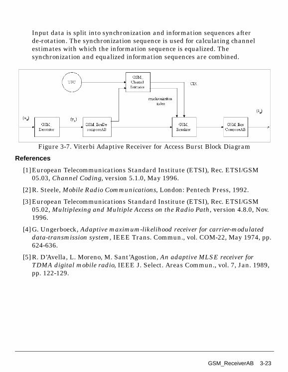
Input data is split into synchronization and information sequences afterde-rotation. The synchronization sequence is used for calculating channelestimates with which the information sequence is equalized. Thesynchronization and equalized information sequences are combined.
Figure 3-7. Viterbi Adaptive Receiver for Access Burst Block Diagram
References
[1]European Telecommunications Standard Institute (ETSI), Rec. ETSI/GSM05.03, Channel Coding, version 5.1.0, May 1996.
[2] R. Steele, Mobile Radio Communications, London: Pentech Press, 1992.
[3] European Telecommunications Standard Institute (ETSI), Rec. ETSI/GSM05.02, Multiplexing and Multiple Access on the Radio Path, version 4.8.0, Nov.1996.
[4] G. Ungerboeck, Adaptive maximum-likelihood receiver for carrier-modulateddata-transmission system, IEEE Trans. Commun., vol. COM-22, May 1974, pp.624-636.
[5] R. D’Avella, L. Moreno, M. Sant’Agostion, An adaptive MLSE receiver forTDMA digital mobile radio, IEEE J. Select. Areas Commun., vol. 7, Jan. 1989,pp. 122-129.
GSM_ReceiverAB 3-23

Chapter 4: Framing Components
4-1
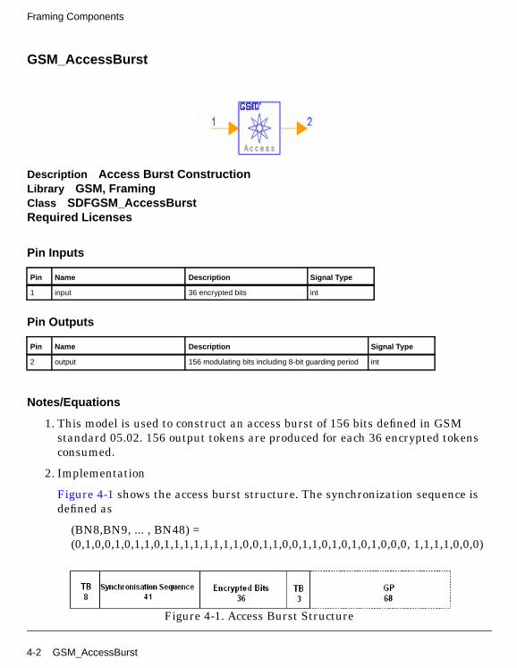
Framing Components
GSM_AccessBurst
Description Access Burst ConstructionLibrary GSM, FramingClass SDFGSM_AccessBurstRequired Licenses
Pin Inputs
Pin Outputs
Notes/Equations
1. This model is used to construct an access burst of 156 bits defined in GSMstandard 05.02. 156 output tokens are produced for each 36 encrypted tokensconsumed.
2. Implementation
Figure 4-1 shows the access burst structure. The synchronization sequence isdefined as
(BN8,BN9, ... , BN48) =(0,1,0,0,1,0,1,1,0,1,1,1,1,1,1,1,1,0,0,1,1,0,0,1,1,0,1,0,1,0,1,0,0,0, 1,1,1,1,0,0,0)
Figure 4-1. Access Burst Structure
Pin Name Description Signal Type
1 input 36 encrypted bits int
Pin Name Description Signal Type
2 output 156 modulating bits including 8-bit guarding period int
4-2 GSM_AccessBurst
References
[1]European Telecommunications Standard Institute (ETSI), Rec. ETSI/GSM05.02, Multiplexing and Multiple Access on the Radio Path, version 3.5.1, March1992.
GSM_AccessBurst 4-3
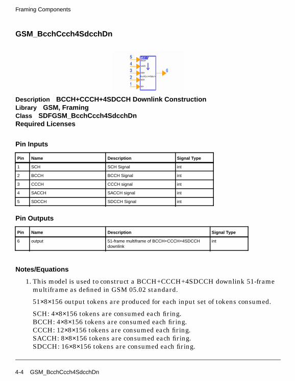
Framing Components
GSM_BcchCcch4SdcchDn
Description BCCH+CCCH+4SDCCH Downlink ConstructionLibrary GSM, FramingClass SDFGSM_BcchCcch4SdcchDnRequired Licenses
Pin Inputs
Pin Outputs
Notes/Equations
1. This model is used to construct a BCCH+CCCH+4SDCCH downlink 51-framemultiframe as defined in GSM 05.02 standard.
51×8×156 output tokens are produced for each input set of tokens consumed.
SCH: 4×8×156 tokens are consumed each firing.BCCH: 4×8×156 tokens are consumed each firing.CCCH: 12×8×156 tokens are consumed each firing.SACCH: 8×8×156 tokens are consumed each firing.SDCCH: 16×8×156 tokens are consumed each firing.
Pin Name Description Signal Type
1 SCH SCH Signal int
2 BCCH BCCH Signal int
3 CCCH CCCH signal int
4 SACCH SACCH signal int
5 SDCCH SDCCH Signal int
Pin Name Description Signal Type
6 output 51-frame multiframe of BCCH+CCCH+4SDCCHdownlink
int
4-4 GSM_BcchCcch4SdcchDn
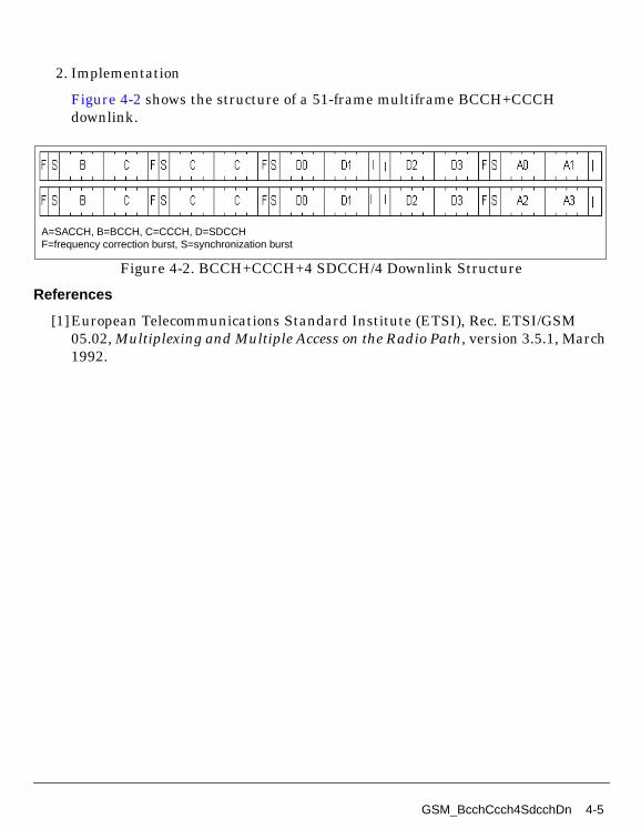
2. Implementation
Figure 4-2 shows the structure of a 51-frame multiframe BCCH+CCCHdownlink.
Figure 4-2. BCCH+CCCH+4 SDCCH/4 Downlink Structure
References
[1]European Telecommunications Standard Institute (ETSI), Rec. ETSI/GSM05.02, Multiplexing and Multiple Access on the Radio Path, version 3.5.1, March1992.
A=SACCH, B=BCCH, C=CCCH, D=SDCCHF=frequency correction burst, S=synchronization burst
GSM_BcchCcch4SdcchDn 4-5
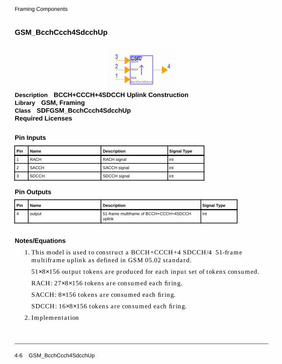
Framing Components
GSM_BcchCcch4SdcchUp
Description BCCH+CCCH+4SDCCH Uplink ConstructionLibrary GSM, FramingClass SDFGSM_BcchCcch4SdcchUpRequired Licenses
Pin Inputs
Pin Outputs
Notes/Equations
1. This model is used to construct a BCCH+CCCH+4 SDCCH/4 51-framemultiframe uplink as defined in GSM 05.02 standard.
51×8×156 output tokens are produced for each input set of tokens consumed.
RACH: 27×8×156 tokens are consumed each firing.
SACCH: 8×156 tokens are consumed each firing.
SDCCH: 16×8×156 tokens are consumed each firing.
2. Implementation
Pin Name Description Signal Type
1 RACH RACH signal int
2 SACCH SACCH signal int
3 SDCCH SDCCH signal int
Pin Name Description Signal Type
4 output 51-frame multiframe of BCCH+CCCH+4SDCCHuplink
int
4-6 GSM_BcchCcch4SdcchUp
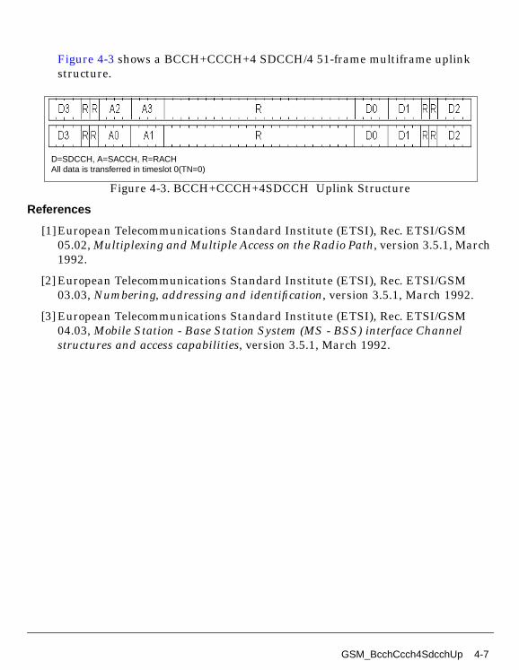
Figure 4-3 shows a BCCH+CCCH+4 SDCCH/4 51-frame multiframe uplinkstructure.
Figure 4-3. BCCH+CCCH+4SDCCH Uplink Structure
References
[1]European Telecommunications Standard Institute (ETSI), Rec. ETSI/GSM05.02, Multiplexing and Multiple Access on the Radio Path, version 3.5.1, March1992.
[2] European Telecommunications Standard Institute (ETSI), Rec. ETSI/GSM03.03, Numbering, addressing and identification, version 3.5.1, March 1992.
[3] European Telecommunications Standard Institute (ETSI), Rec. ETSI/GSM04.03, Mobile Station - Base Station System (MS - BSS) interface Channelstructures and access capabilities, version 3.5.1, March 1992.
D=SDCCH, A=SACCH, R=RACHAll data is transferred in timeslot 0(TN=0)
GSM_BcchCcch4SdcchUp 4-7
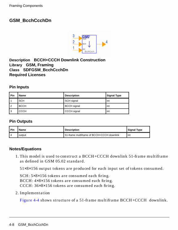
Framing Components
GSM_BcchCcchDn
Description BCCH+CCCH Downlink ConstructionLibrary GSM, FramingClass SDFGSM_BcchCcchDnRequired Licenses
Pin Inputs
Pin Outputs
Notes/Equations
1. This model is used to construct a BCCH+CCCH downlink 51-frame multiframeas defined in GSM 05.02 standard.
51×8×156 output tokens are produced for each input set of tokens consumed.
SCH: 5×8×156 tokens are consumed each firing.BCCH: 4×8×156 tokens are consumed each firing.CCCH: 36×8×156 tokens are consumed each firing.
2. Implementation
Figure 4-4 shows structure of a 51-frame multiframe BCCH+CCCH downlink.
Pin Name Description Signal Type
1 SCH SCH signal int
2 BCCH BCCH signal int
3 CCCH CCCH signal int
Pin Name Description Signal Type
4 output 51-frame multiframe of BCCH+CCCH downlink int
4-8 GSM_BcchCcchDn
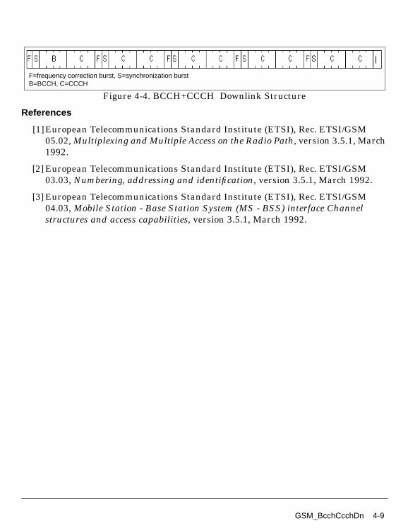
Figure 4-4. BCCH+CCCH Downlink Structure
References
[1]European Telecommunications Standard Institute (ETSI), Rec. ETSI/GSM05.02, Multiplexing and Multiple Access on the Radio Path, version 3.5.1, March1992.
[2] European Telecommunications Standard Institute (ETSI), Rec. ETSI/GSM03.03, Numbering, addressing and identification, version 3.5.1, March 1992.
[3] European Telecommunications Standard Institute (ETSI), Rec. ETSI/GSM04.03, Mobile Station - Base Station System (MS - BSS) interface Channelstructures and access capabilities, version 3.5.1, March 1992.
F=frequency correction burst, S=synchronization burstB=BCCH, C=CCCH
GSM_BcchCcchDn 4-9
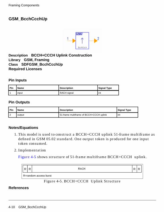
Framing Components
GSM_BcchCcchUp
Description BCCH+CCCH Uplink ConstructionLibrary GSM, FramingClass SDFGSM_BcchCcchUpRequired Licenses
Pin Inputs
Pin Outputs
Notes/Equations
1. This model is used to construct a BCCH+CCCH uplink 51-frame multiframe asdefined in GSM 05.02 standard. One output token is produced for one inputtoken consumed.
2. Implementation
Figure 4-5 shows structure of 51-frame multiframe BCCH+CCCH uplink.
Figure 4-5. BCCH+CCCH Uplink Structure
References
Pin Name Description Signal Type
1 input RACH signal int
Pin Name Description Signal Type
2 output 51-frame multiframe of BCCH+CCCH uplink int
R=random access burst
4-10 GSM_BcchCcchUp
[1]European Telecommunications Standard Institute (ETSI), Rec. ETSI/GSM05.02, Multiplexing and Multiple Access on the Radio Path, version 3.5.1, March1992.
[2] European Telecommunications Standard Institute (ETSI), Rec. ETSI/GSM03.03, Numbering, addressing and identification, version 3.5.1, March 1992.
[3] European Telecommunications Standard Institute (ETSI), Rec. ETSI/GSM04.03, Mobile Station - Base Station System (MS - BSS) interface Channelstructures and access capabilities, version 3.5.1, March 1992.
GSM_BcchCcchUp 4-11

Framing Components
GSM_DeAccessBurst
Description Access Burst DisassemblyLibrary GSM, FramingClass SDFGSM_DeAccessBurstRequired Licenses
Pin Inputs
Pin Outputs
Notes/Equations/References
1. This model is used to disassemble the access burst as defined in GSM 05.02standard.
36 output tokens are produced for each 156 tokens consumed.
2. Implementation
Figure 4-6 shows the access burst structure.
Figure 4-6. Access Burst Structure
References
Pin Name Description Signal Type
1 input 156 bits of access burst real
Pin Name Description Signal Type
2 output 36 encrypted bits real
4-12 GSM_DeAccessBurst
[1]European Telecommunications Standard Institute (ETSI), Rec. ETSI/GSM05.02, Multiplexing and Multiple Access on the Radio Path, version 3.5.1, March1992.
[2] European Telecommunications Standard Institute (ETSI), Rec. ETSI/GSM03.03, Numbering, addressing and identification, version 3.5.1, March 1992.
[3] European Telecommunications Standard Institute (ETSI), Rec. ETSI/GSM04.03, Mobile Station - Base Station System (MS - BSS) interface Channelstructures and access capabilities, version 3.5.1, March 1992.
GSM_DeAccessBurst 4-13
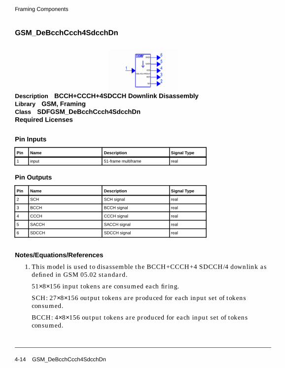
Framing Components
GSM_DeBcchCcch4SdcchDn
Description BCCH+CCCH+4SDCCH Downlink DisassemblyLibrary GSM, FramingClass SDFGSM_DeBcchCcch4SdcchDnRequired Licenses
Pin Inputs
Pin Outputs
Notes/Equations/References
1. This model is used to disassemble the BCCH+CCCH+4 SDCCH/4 downlink asdefined in GSM 05.02 standard.
51×8×156 input tokens are consumed each firing.
SCH: 27×8×156 output tokens are produced for each input set of tokensconsumed.
BCCH: 4×8×156 output tokens are produced for each input set of tokensconsumed.
Pin Name Description Signal Type
1 input 51-frame multiframe real
Pin Name Description Signal Type
2 SCH SCH signal real
3 BCCH BCCH signal real
4 CCCH CCCH signal real
5 SACCH SACCH signal real
6 SDCCH SDCCH signal real
4-14 GSM_DeBcchCcch4SdcchDn

CCCH: 12×8×156 output tokens are produced for each input set of tokensconsumed.
SACCH: 8×8×156 output tokens are produced for each input set of tokensconsumed.
SDCCH: 16×8×156 output tokens are produced for each input set of tokensconsumed.
2. Implementation
Figure 4-7 shows structure of 51-frame multiframe BCCH+CCCH+4SDCCHdownlink.
Figure 4-7. BCCH+CCCH+4 SDCCH/4 Downlink Structure
References
[1]European Telecommunications Standard Institute (ETSI), Rec. ETSI/GSM05.02, Multiplexing and Multiple Access on the Radio Path, version 3.5.1, March1992.
[2] European Telecommunications Standard Institute (ETSI), Rec. ETSI/GSM03.03, Numbering, addressing and identification, version 3.5.1, March 1992.
[3] European Telecommunications Standard Institute (ETSI), Rec. ETSI/GSM04.03, Mobile Station - Base Station System (MS - BSS) interface Channelstructures and access capabilities, version 3.5.1, March 1992.
D=SDCCH, A=SACCH, B=BCCH, C=CCCHF=frequency correction burst, S=synchronization burst
GSM_DeBcchCcch4SdcchDn 4-15
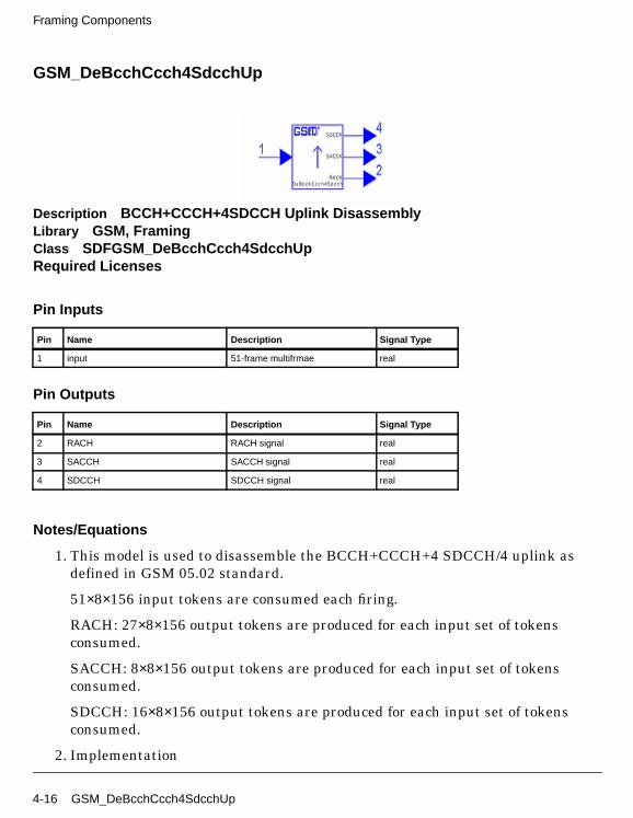
Framing Components
GSM_DeBcchCcch4SdcchUp
Description BCCH+CCCH+4SDCCH Uplink DisassemblyLibrary GSM, FramingClass SDFGSM_DeBcchCcch4SdcchUpRequired Licenses
Pin Inputs
Pin Outputs
Notes/Equations
1. This model is used to disassemble the BCCH+CCCH+4 SDCCH/4 uplink asdefined in GSM 05.02 standard.
51×8×156 input tokens are consumed each firing.
RACH: 27×8×156 output tokens are produced for each input set of tokensconsumed.
SACCH: 8×8×156 output tokens are produced for each input set of tokensconsumed.
SDCCH: 16×8×156 output tokens are produced for each input set of tokensconsumed.
2. Implementation
Pin Name Description Signal Type
1 input 51-frame multifrmae real
Pin Name Description Signal Type
2 RACH RACH signal real
3 SACCH SACCH signal real
4 SDCCH SDCCH signal real
4-16 GSM_DeBcchCcch4SdcchUp
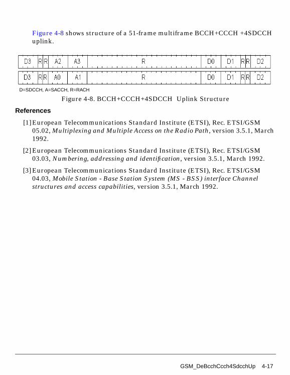
Figure 4-8 shows structure of a 51-frame multiframe BCCH+CCCH +4SDCCHuplink.
Figure 4-8. BCCH+CCCH+4SDCCH Uplink Structure
References
[1]European Telecommunications Standard Institute (ETSI), Rec. ETSI/GSM05.02, Multiplexing and Multiple Access on the Radio Path, version 3.5.1, March1992.
[2] European Telecommunications Standard Institute (ETSI), Rec. ETSI/GSM03.03, Numbering, addressing and identification, version 3.5.1, March 1992.
[3] European Telecommunications Standard Institute (ETSI), Rec. ETSI/GSM04.03, Mobile Station - Base Station System (MS - BSS) interface Channelstructures and access capabilities, version 3.5.1, March 1992.
D=SDCCH, A=SACCH, R=RACH
GSM_DeBcchCcch4SdcchUp 4-17

Framing Components
GSM_DeBcchCcchDn
Description BCCH+CCCH Downlink DisassemblyLibrary GSM, FramingClass SDFGSM_DeBcchCcchDnRequired Licenses
Pin Inputs
Pin Outputs
Notes/Equations
1. This model is used to disassemble a BCCH+CCCH downlink 51-framemultiframe as defined in GSM 05.02 standard.
51×8×156 input tokens are consumed each firing.
SCH: 5×8×156 output tokens are produced for each input set of tokensconsumed.
BCCH: 4×8×156 output tokens are produced for each input set of tokensconsumed.
CCCH: 36×8×156 output tokens are produced for each input set of tokensconsumed.
2. Implementation
Pin Name Description Signal Type
1 input 51-frame multiframe real
Pin Name Description Signal Type
2 SCH SCH signal real
3 BCCH BCCH signal real
4 CCCH CCCH signal real
4-18 GSM_DeBcchCcchDn
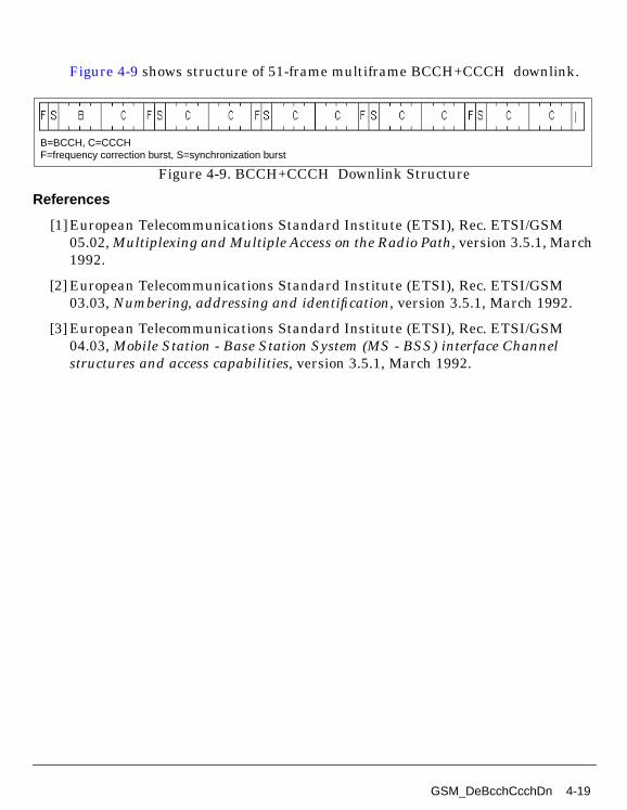
Figure 4-9 shows structure of 51-frame multiframe BCCH+CCCH downlink.
Figure 4-9. BCCH+CCCH Downlink Structure
References
[1]European Telecommunications Standard Institute (ETSI), Rec. ETSI/GSM05.02, Multiplexing and Multiple Access on the Radio Path, version 3.5.1, March1992.
[2] European Telecommunications Standard Institute (ETSI), Rec. ETSI/GSM03.03, Numbering, addressing and identification, version 3.5.1, March 1992.
[3] European Telecommunications Standard Institute (ETSI), Rec. ETSI/GSM04.03, Mobile Station - Base Station System (MS - BSS) interface Channelstructures and access capabilities, version 3.5.1, March 1992.
B=BCCH, C=CCCHF=frequency correction burst, S=synchronization burst
GSM_DeBcchCcchDn 4-19
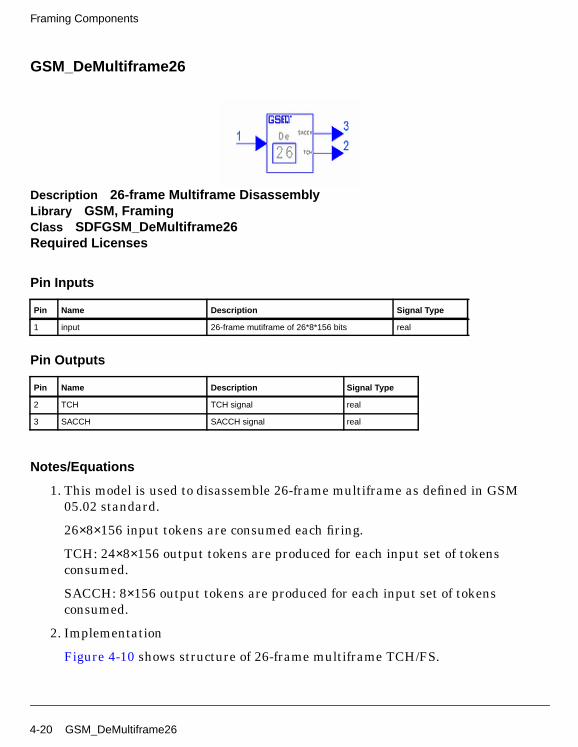
Framing Components
GSM_DeMultiframe26
Description 26-frame Multiframe DisassemblyLibrary GSM, FramingClass SDFGSM_DeMultiframe26Required Licenses
Pin Inputs
Pin Outputs
Notes/Equations
1. This model is used to disassemble 26-frame multiframe as defined in GSM05.02 standard.
26×8×156 input tokens are consumed each firing.
TCH: 24×8×156 output tokens are produced for each input set of tokensconsumed.
SACCH: 8×156 output tokens are produced for each input set of tokensconsumed.
2. Implementation
Figure 4-10 shows structure of 26-frame multiframe TCH/FS.
Pin Name Description Signal Type
1 input 26-frame mutiframe of 26*8*156 bits real
Pin Name Description Signal Type
2 TCH TCH signal real
3 SACCH SACCH signal real
4-20 GSM_DeMultiframe26
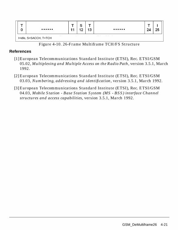
Figure 4-10. 26-Frame Multiframe TCH/FS Structure
References
[1]European Telecommunications Standard Institute (ETSI), Rec. ETSI/GSM05.02, Multiplexing and Multiple Access on the Radio Path, version 3.5.1, March1992.
[2] European Telecommunications Standard Institute (ETSI), Rec. ETSI/GSM03.03, Numbering, addressing and identification, version 3.5.1, March 1992.
[3] European Telecommunications Standard Institute (ETSI), Rec. ETSI/GSM04.03, Mobile Station - Base Station System (MS - BSS) interface Channelstructures and access capabilities, version 3.5.1, March 1992.
I=idle, S=SACCH, T=TCH
GSM_DeMultiframe26 4-21
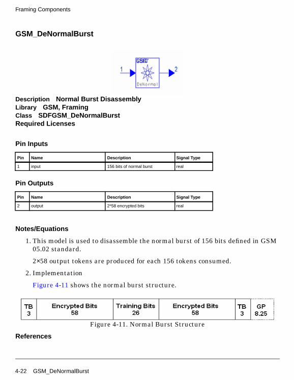
Framing Components
GSM_DeNormalBurst
Description Normal Burst DisassemblyLibrary GSM, FramingClass SDFGSM_DeNormalBurstRequired Licenses
Pin Inputs
Pin Outputs
Notes/Equations
1. This model is used to disassemble the normal burst of 156 bits defined in GSM05.02 standard.
2×58 output tokens are produced for each 156 tokens consumed.
2. Implementation
Figure 4-11 shows the normal burst structure.
Figure 4-11. Normal Burst Structure
References
Pin Name Description Signal Type
1 input 156 bits of normal burst real
Pin Name Description Signal Type
2 output 2*58 encrypted bits real
4-22 GSM_DeNormalBurst

[1]European Telecommunications Standard Institute (ETSI), Rec. ETSI/GSM05.02, Multiplexing and Multiple Access on the Radio Path, version 3.5.1, March1992.
[2] European Telecommunications Standard Institute (ETSI), Rec. ETSI/GSM03.03, Numbering, addressing and identification, version 3.5.1, March 1992.
[3] European Telecommunications Standard Institute (ETSI), Rec. ETSI/GSM04.03, Mobile Station - Base Station System (MS - BSS) interface Channelstructures and access capabilities, version 3.5.1, March 1992.
GSM_DeNormalBurst 4-23
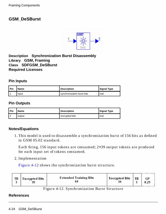
Framing Components
GSM_DeSBurst
Description Synchronization Burst DisassemblyLibrary GSM, FramingClass SDFGSM_DeSBurstRequired Licenses
Pin Inputs
Pin Outputs
Notes/Equations
1. This model is used to disassemble a synchronization burst of 156 bits as definedin GSM 05.02 standard.
Each firing, 156 input tokens are consumed; 2×39 output tokens are producedfor each input set of tokens consumed.
2. Implementation
Figure 4-12 shows the synchronization burst structure.
Figure 4-12. Synchronization Burst Structure
References
Pin Name Description Signal Type
1 input synchronization burst bits real
Pin Name Description Signal Type
2 output encrypted bits real
4-24 GSM_DeSBurst
[1]European Telecommunications Standard Institute (ETSI), Rec. ETSI/GSM05.02, Multiplexing and Multiple Access on the Radio Path, version 3.5.1, March1992.
[2] European Telecommunications Standard Institute (ETSI), Rec. ETSI/GSM03.03, Numbering, addressing and identification, version 3.5.1, March 1992.
[3] European Telecommunications Standard Institute (ETSI), Rec. ETSI/GSM04.03, Mobile Station - Base Station System (MS - BSS) interface Channelstructures and access capabilities, version 3.5.1, March 1992.
GSM_DeSBurst 4-25

Framing Components
GSM_DeSdcch8Dn
Description 8SDCCH/8 Downlink DisassemblyLibrary GSM, FramingClass SDFGSM_DeSdcch8DnRequired Licenses
Pin Inputs
Pin Outputs
Notes/Equations
1. This model is used to disassemble an 8SDCCH/8 downlink 51-frame multiframeas defined in GSM 05.02 standard.
51×8×156 input tokens are consumed each firing.
SACCH: 16×8×156 output tokens are produced for each input set of tokensconsumed.
SDCCH: 32×8×156 output tokens are produced for each input set of tokensconsumed.
2. Implementation
Figure 4-13 shows structure of 51-frame multiframe 8SDCCH/8 downlink.
Pin Name Description Signal Type
1 input 51-frame multiframe of 51*8*156 bits real
Pin Name Description Signal Type
2 SACCH SACCH signal real
3 SDCCH SDCCH signal real
4-26 GSM_DeSdcch8Dn

Figure 4-13. 8SDCCH/8 Downlink Structure
References
[1]European Telecommunications Standard Institute (ETSI), Rec. ETSI/GSM05.02, Multiplexing and Multiple Access on the Radio Path, version 3.5.1, March1992.
[2] European Telecommunications Standard Institute (ETSI), Rec. ETSI/GSM03.03, Numbering, addressing and identification, version 3.5.1, March 1992.
[3] European Telecommunications Standard Institute (ETSI), Rec. ETSI/GSM04.03, Mobile Station - Base Station System (MS - BSS) interface Channelstructures and access capabilities, version 3.5.1, March 1992.
A=SACCH, D=SDCCHI=idle frame
GSM_DeSdcch8Dn 4-27
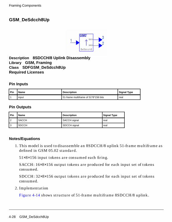
Framing Components
GSM_DeSdcch8Up
Description 8SDCCH/8 Uplink DisassemblyLibrary GSM, FramingClass SDFGSM_DeSdcch8UpRequired Licenses
Pin Inputs
Pin Outputs
Notes/Equations
1. This model is used to disassemble an 8SDCCH/8 uplink 51-frame multiframe asdefined in GSM 05.02 standard.
51×8×156 input tokens are consumed each firing.
SACCH: 16×8×156 output tokens are produced for each input set of tokensconsumed.
SDCCH: 32×8×156 output tokens are produced for each input set of tokensconsumed.
2. Implementation
Figure 4-14 shows structure of 51-frame multiframe 8SDCCH/8 uplink.
Pin Name Description Signal Type
1 input 51-frame multiframe of 51*8*156 bits real
Pin Name Description Signal Type
2 SACCH SACCH signal real
3 SDCCH SDCCH signal real
4-28 GSM_DeSdcch8Up

Figure 4-14. 8SDCCH/8 Uplink Structure
References
[1]European Telecommunications Standard Institute (ETSI), Rec. ETSI/GSM05.02, Multiplexing and Multiple Access on the Radio Path, version 3.5.1, March1992.
[2] European Telecommunications Standard Institute (ETSI), Rec. ETSI/GSM03.03, Numbering, addressing and identification, version 3.5.1, March 1992.
[3] European Telecommunications Standard Institute (ETSI), Rec. ETSI/GSM04.03, Mobile Station - Base Station System (MS - BSS) interface Channelstructures and access capabilities, version 3.5.1, March 1992.
A=SACCH, D=SDCCHI=idle frame
GSM_DeSdcch8Up 4-29

Framing Components
GSM_DeTDMA
Description TDMA Frame DisassemblyLibrary GSM, FramingRequired Licenses
Pin Inputs
Pin Outputs
Notes/Equations
1. This model is used to disassemble a TDMA frame into 8 time slots as defined inGSM 05.02 standard.
2. Implementation
In GSM standard, one TDMA frame contains 8 time slots TN0 to TN7. The userselects a time slot to fill with input data; the idle time slots will be filled with 0.For example, Figure 4-15 shows TN2 and TN4 selected, the first 156 input bits
Pin Name Description Signal Type
1 input one TDMA frame of eight time slots anytype
Pin Name Description Signal Type
2 O_TN7 data for time slot 7 anytype
3 O_TN6 data for time slot 6 anytype
4 O_TN5 data for time slot 5 anytype
5 O_TN4 data for time slot 4 anytype
6 O_TN3 data for time slot 3 anytype
7 O_TN2 data for time slot 2 anytype
8 O_TN1 data for time slot 1 anytype
9 O_TN0 data for time slot 0 anytype
4-30 GSM_DeTDMA
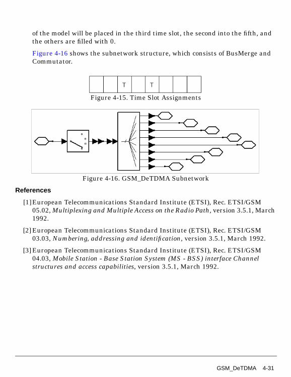
of the model will be placed in the third time slot, the second into the fifth, andthe others are filled with 0.
Figure 4-16 shows the subnetwork structure, which consists of BusMerge andCommutator.
Figure 4-15. Time Slot Assignments
Figure 4-16. GSM_DeTDMA Subnetwork
References
[1]European Telecommunications Standard Institute (ETSI), Rec. ETSI/GSM05.02, Multiplexing and Multiple Access on the Radio Path, version 3.5.1, March1992.
[2] European Telecommunications Standard Institute (ETSI), Rec. ETSI/GSM03.03, Numbering, addressing and identification, version 3.5.1, March 1992.
[3] European Telecommunications Standard Institute (ETSI), Rec. ETSI/GSM04.03, Mobile Station - Base Station System (MS - BSS) interface Channelstructures and access capabilities, version 3.5.1, March 1992.
GSM_DeTDMA 4-31
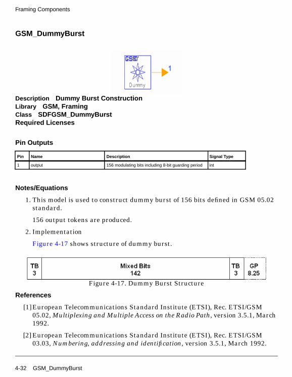
Framing Components
GSM_DummyBurst
Description Dummy Burst ConstructionLibrary GSM, FramingClass SDFGSM_DummyBurstRequired Licenses
Pin Outputs
Notes/Equations
1. This model is used to construct dummy burst of 156 bits defined in GSM 05.02standard.
156 output tokens are produced.
2. Implementation
Figure 4-17 shows structure of dummy burst.
Figure 4-17. Dummy Burst Structure
References
[1]European Telecommunications Standard Institute (ETSI), Rec. ETSI/GSM05.02, Multiplexing and Multiple Access on the Radio Path, version 3.5.1, March1992.
[2] European Telecommunications Standard Institute (ETSI), Rec. ETSI/GSM03.03, Numbering, addressing and identification, version 3.5.1, March 1992.
Pin Name Description Signal Type
1 output 156 modulating bits including 8-bit guarding period int
4-32 GSM_DummyBurst
[3] European Telecommunications Standard Institute (ETSI), Rec. ETSI/GSM04.03, Mobile Station - Base Station System (MS - BSS) interface Channelstructures and access capabilities, version 3.5.1, March 1992.
GSM_DummyBurst 4-33
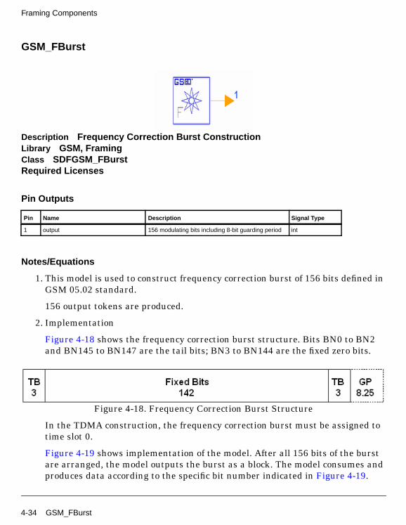
Framing Components
GSM_FBurst
Description Frequency Correction Burst ConstructionLibrary GSM, FramingClass SDFGSM_FBurstRequired Licenses
Pin Outputs
Notes/Equations
1. This model is used to construct frequency correction burst of 156 bits defined inGSM 05.02 standard.
156 output tokens are produced.
2. Implementation
Figure 4-18 shows the frequency correction burst structure. Bits BN0 to BN2and BN145 to BN147 are the tail bits; BN3 to BN144 are the fixed zero bits.
Figure 4-18. Frequency Correction Burst Structure
In the TDMA construction, the frequency correction burst must be assigned totime slot 0.
Figure 4-19 shows implementation of the model. After all 156 bits of the burstare arranged, the model outputs the burst as a block. The model consumes andproduces data according to the specific bit number indicated in Figure 4-19.
Pin Name Description Signal Type
1 output 156 modulating bits including 8-bit guarding period int
4-34 GSM_FBurst
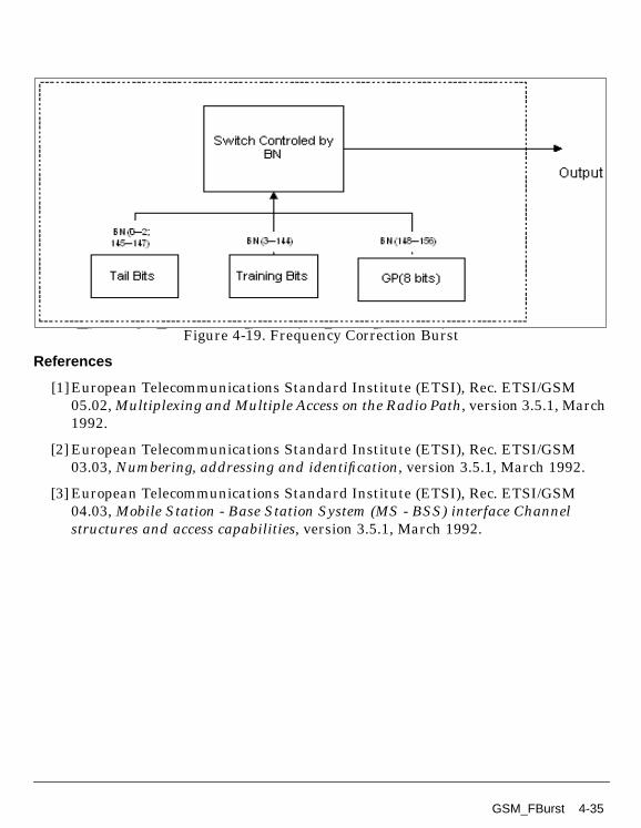
Figure 4-19. Frequency Correction Burst
References
[1]European Telecommunications Standard Institute (ETSI), Rec. ETSI/GSM05.02, Multiplexing and Multiple Access on the Radio Path, version 3.5.1, March1992.
[2] European Telecommunications Standard Institute (ETSI), Rec. ETSI/GSM03.03, Numbering, addressing and identification, version 3.5.1, March 1992.
[3] European Telecommunications Standard Institute (ETSI), Rec. ETSI/GSM04.03, Mobile Station - Base Station System (MS - BSS) interface Channelstructures and access capabilities, version 3.5.1, March 1992.
GSM_FBurst 4-35

Framing Components
GSM_Multiframe26
Description 26-frame Multiframe ConstructionLibrary GSM, FramingClass SDFGSM_Multiframe26Required Licenses
Pin Inputs
Pin Outputs
Notes/Equations
1. This model is used to construct 26-frame multiframe defined in GSM 05.02standard.
26×8×156 output tokens are produced each firing.TCH: 24×8×156 input tokens are consumed each firing.SACCH: 8×156 input tokens are consumed each firing.
2. Implementation
Figure 4-20 shows the 26-multiframe structure. One 26-frame multiframeconsists of 26 TDMA frames.
Pin Name Description Signal Type
1 TCH TCH signal int
2 SACCH SACCH signal int
Pin Name Description Signal Type
3 output 26-frame multiframe int
4-36 GSM_Multiframe26
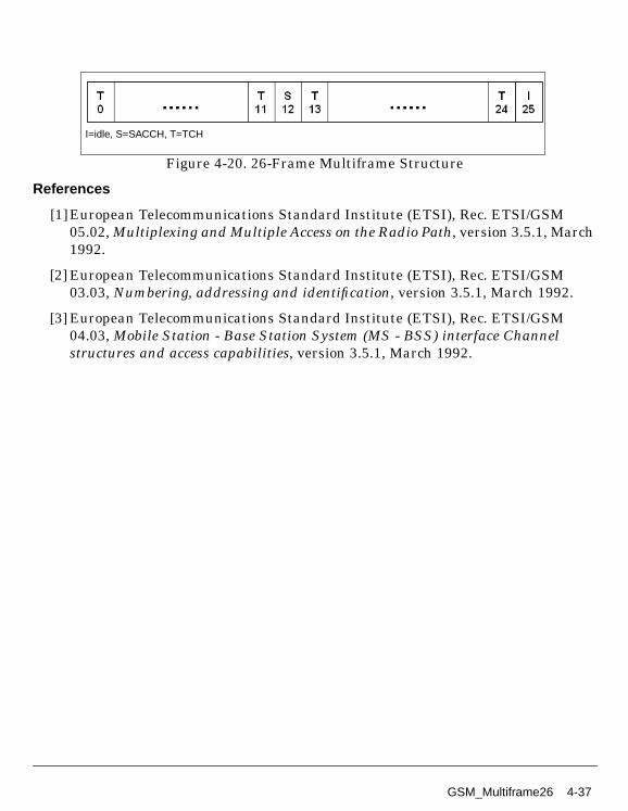
Figure 4-20. 26-Frame Multiframe Structure
References
[1]European Telecommunications Standard Institute (ETSI), Rec. ETSI/GSM05.02, Multiplexing and Multiple Access on the Radio Path, version 3.5.1, March1992.
[2] European Telecommunications Standard Institute (ETSI), Rec. ETSI/GSM03.03, Numbering, addressing and identification, version 3.5.1, March 1992.
[3] European Telecommunications Standard Institute (ETSI), Rec. ETSI/GSM04.03, Mobile Station - Base Station System (MS - BSS) interface Channelstructures and access capabilities, version 3.5.1, March 1992.
I=idle, S=SACCH, T=TCH
GSM_Multiframe26 4-37

Framing Components
GSM_NormalBurst
Description Normal Burst ConstructionLibrary GSM, FramingClass SDFGSM_NormalBurstRequired Licenses
Parameters
Pin Inputs
Pin Outputs
Notes/Equations
1. The model is used to construct a normal burst of 156 bits as defined in GSM05.02 standard.
156 output tokens are produced for each 2×58 tokens consumed.
2. Implementation
Figure 4-21 shows the normal burst structure. Bits BN0 to BN2 and BN145 toBN147 are tail bits; BN3 to BN60 and BN87 to BN144 are encrypted bits thatare outputs of channel coding models; BN61 to BN86 are training bits.
Name Description Default Type Range
TSC training sequence code,varies from 0 to 7.
0 int [0, 7]
Pin Name Description Signal Type
1 input 2*58 information bits int
Pin Name Description Signal Type
2 output 156 modulating bits with 8-bit guarding period int
4-38 GSM_NormalBurst
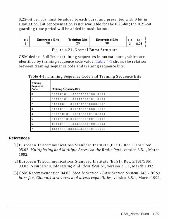
8.25-bit periods must be added to each burst and presented with 0 bit insimulation. Bit representation is not available for the 0.25-bit; the 0.25-bitguarding time period will be added in modulation.
Figure 4-21. Normal Burst Structure
GSM defines 8 different training sequences in normal burst, which areidentified by training sequence code value. Table 4-1 shows the relationbetween training sequence code and training sequence bits.
References
[1]European Telecommunications Standard Institute (ETSI), Rec. ETSI/GSM05.02, Multiplexing and Multiple Access on the Radio Path, version 3.5.1, March1992.
[2] European Telecommunications Standard Institute (ETSI), Rec. ETSI/GSM03.03, Numbering, addressing and identification, version 3.5.1, March 1992.
[3] GSM Recommendation 04.03, Mobile Station - Base Station System (MS - BSS)inter face Channel structures and access capabilities, version 3.5.1, March 1992.
Table 4-1. Training Sequence Code and Training Sequence Bits
TrainingSequenceCode Training Sequence Bits
0 0,0,1,0,0,1,0,1,1,1,0,0,0,0,1,0,0,0,1,0,0,1,0,1,1,1
1 0,0,1,0,1,1,0,1,1,1,0,1,1,1,1,0,0,0,1,0,1,1,0,1,1,1
2 0,1,0,0,0,0,1,1,1,0,1,1,1,0,1,0,0,1,0,0,0,0,1,1,1,0
3 0,1,0,0,0,1,1,1,1,0,1,1,0,1,0,0,0,1,0,0,0,1,1,1,1,0
4 0,0,0,1,1,0,1,0,1,1,1,0,0,1,0,0,0,0,0,1,1,0,1,0,1,1
5 0,1,0,0,1,1,1,0,1,0,1,1,0,0,0,0,0,1,0,0,1,1,1,0,1,0
6 1,0,1,0,0,1,1,1,1,1,0,1,1,0,0,0,1,0,1,0,0,1,1,1,1,1
7 1,1,1,0,1,1,1,1,0,0,0,1,0,0,1,0,1,1,1,0,1,1,1,1,0,0
GSM_NormalBurst 4-39

Framing Components
GSM_SBurst
Description Synchronization Burst ConstructionLibrary GSM, FramingClass SDFGSM_SBurstRequired Licenses
Pin Inputs
Pin Outputs
Notes/Equations
3. The model is used to construct synchronization burst of 156 bits defined in GSM05.02 standard.
156 output tokens are produced for each 2×39 tokens consumed.
4. Implementation
Figure 4-22 shows the synchronization burst structure.
Figure 4-22. Synchronization Burst Structure
In the TDMA construction, the frequency correction burst must be assigned totime slot 0.
Pin Name Description Signal Type
1 input 2*39 encrypted bits int
Pin Name Description Signal Type
2 output 156 modulating bits including 8-bit guarding period int
4-40 GSM_SBurst
The extended training bits are defined as
(BN42, BN43, ... , BN105)=(1,0,1,1,1,0,0,1,0,1,1,0,0,0,1,0,0,0,0,0,0,1,0,0,0,0,0,0,1,1,1,1,0,0,1,0,1,1,0,1,0,1,0,0,0,1,0,1,0,1,1,1,0,1,1,0,0,0,0,1,1,0,1,1)
References
[1]European Telecommunications Standard Institute (ETSI), Rec. ETSI/GSM05.02, Multiplexing and Multiple Access on the Radio Path, version 3.5.1, March1992.
[2] European Telecommunications Standard Institute (ETSI), Rec. ETSI/GSM03.03, Numbering, addressing and identification, version 3.5.1, March 1992.
[3] European Telecommunications Standard Institute (ETSI), Rec. ETSI/GSM04.03, Mobile Station - Base Station System (MS - BSS) interface Channelstructures and access capabilities, version 3.5.1, March 1992.
GSM_SBurst 4-41
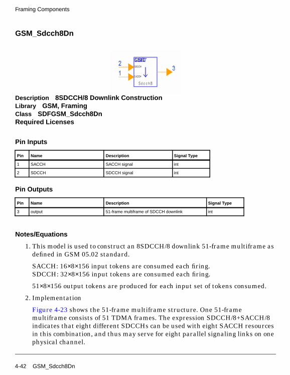
Framing Components
GSM_Sdcch8Dn
Description 8SDCCH/8 Downlink ConstructionLibrary GSM, FramingClass SDFGSM_Sdcch8DnRequired Licenses
Pin Inputs
Pin Outputs
Notes/Equations
1. This model is used to construct an 8SDCCH/8 downlink 51-frame multiframe asdefined in GSM 05.02 standard.
SACCH: 16×8×156 input tokens are consumed each firing.SDCCH: 32×8×156 input tokens are consumed each firing.
51×8×156 output tokens are produced for each input set of tokens consumed.
2. Implementation
Figure 4-23 shows the 51-frame multiframe structure. One 51-framemultiframe consists of 51 TDMA frames. The expression SDCCH/8+SACCH/8indicates that eight different SDCCHs can be used with eight SACCH resourcesin this combination, and thus may serve for eight parallel signaling links on onephysical channel.
Pin Name Description Signal Type
1 SACCH SACCH signal int
2 SDCCH SDCCH signal int
Pin Name Description Signal Type
3 output 51-frame multiframe of SDCCH downlink int
4-42 GSM_Sdcch8Dn
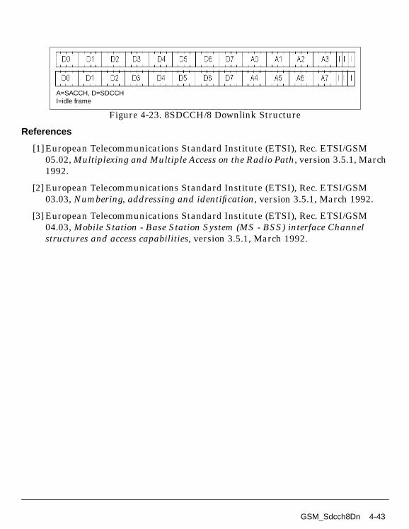
Figure 4-23. 8SDCCH/8 Downlink Structure
References
[1]European Telecommunications Standard Institute (ETSI), Rec. ETSI/GSM05.02, Multiplexing and Multiple Access on the Radio Path, version 3.5.1, March1992.
[2] European Telecommunications Standard Institute (ETSI), Rec. ETSI/GSM03.03, Numbering, addressing and identification, version 3.5.1, March 1992.
[3] European Telecommunications Standard Institute (ETSI), Rec. ETSI/GSM04.03, Mobile Station - Base Station System (MS - BSS) interface Channelstructures and access capabilities, version 3.5.1, March 1992.
A=SACCH, D=SDCCHI=idle frame
GSM_Sdcch8Dn 4-43
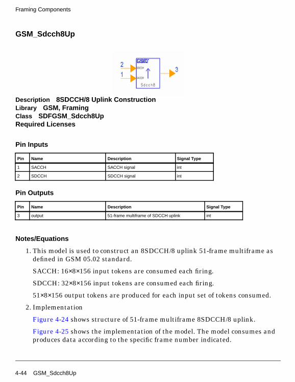
Framing Components
GSM_Sdcch8Up
Description 8SDCCH/8 Uplink ConstructionLibrary GSM, FramingClass SDFGSM_Sdcch8UpRequired Licenses
Pin Inputs
Pin Outputs
Notes/Equations
1. This model is used to construct an 8SDCCH/8 uplink 51-frame multiframe asdefined in GSM 05.02 standard.
SACCH: 16×8×156 input tokens are consumed each firing.
SDCCH: 32×8×156 input tokens are consumed each firing.
51×8×156 output tokens are produced for each input set of tokens consumed.
2. Implementation
Figure 4-24 shows structure of 51-frame multiframe 8SDCCH/8 uplink.
Figure 4-25 shows the implementation of the model. The model consumes andproduces data according to the specific frame number indicated.
Pin Name Description Signal Type
1 SACCH SACCH signal int
2 SDCCH SDCCH signal int
Pin Name Description Signal Type
3 output 51-frame multiframe of SDCCH uplink int
4-44 GSM_Sdcch8Up
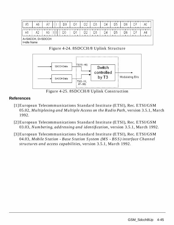
Figure 4-24. 8SDCCH/8 Uplink Structure
Figure 4-25. 8SDCCH/8 Uplink Construction
References
[1]European Telecommunications Standard Institute (ETSI), Rec. ETSI/GSM05.02, Multiplexing and Multiple Access on the Radio Path, version 3.5.1, March1992.
[2] European Telecommunications Standard Institute (ETSI), Rec. ETSI/GSM03.03, Numbering, addressing and identification, version 3.5.1, March 1992.
[3] European Telecommunications Standard Institute (ETSI), Rec. ETSI/GSM04.03, Mobile Station - Base Station System (MS - BSS) interface Channelstructures and access capabilities, version 3.5.1, March 1992.
A=SACCH, D=SDCCHI=idle frame
GSM_Sdcch8Up 4-45

Framing Components
GSM_TDMA
Description TDMA Frame ConstructionLibrary GSM, FramingRequired Licenses
Pin Inputs
Pin Outputs
Notes/Equations
1. This subnetwork is used to construct one TDMA frame as defined in GSM 05.02standard.
2. Implementation
In GSM standard, one TDMA frame contains eight time slots TN0 to TN7; theuser selects which time slots to fill with input data; the idle time slots will befilled with 0. Figure 4-26 shows TN2 and TN4 are selected, the first 156 input
Pin Name Description Signal Type
1 TN7 data for time slot 7 anytype
2 TN6 data for time slot 6 anytype
3 TN5 data for time slot 5 anytype
4 TN4 data for time slot 4 anytype
5 TN3 data for time slot 3 anytype
6 TN2 data for time slot 2 anytype
7 TN1 data for time slot 1 anytype
8 TN0 data for time slot 0 anytype
Pin Name Description Signal Type
9 output one TDMA frame of consist of 8 time slots anytype
4-46 GSM_TDMA

bits of the subnetwork will be placed in the third time slot, the second into thefifth, the rest will be filled with 0.
Figure 4-27 shows the structure of the subnetwork; it consists of Busmerge andCommutator.
Figure 4-26. Time Slot Assignments
Figure 4-27. GSM_TDMA Subnetwork
References
[1]European Telecommunications Standard Institute (ETSI), Rec. ETSI/GSM05.02, Multiplexing and Multiple Access on the Radio Path, version 3.5.1, March1992.
[2] European Telecommunications Standard Institute (ETSI), Rec. ETSI/GSM03.03, Numbering, addressing and identification, version 3.5.1, March 1992.
[3] European Telecommunications Standard Institute (ETSI), Rec. ETSI/GSM04.03, Mobile Station - Base Station System (MS - BSS) interface Channelstructures and access capabilities, version 3.5.1, March 1992.
GSM_TDMA 4-47
Framing Components
GSM_TimeBaseCounter
Description Time Base Counter for T1, T2, T3Library GSM, FramingClass SDFGSM_TimeBaseCounterRequired Licenses
Pin Inputs
Pin Outputs
Notes/Equations
1. This model is used to perform as GSM timebase counters for counting T1, T2,and T3 as defined in GSM 05.02 standard. One token of T1, T2, and T3 areproduced for each 8×156 input tokens consumed.
2. Implementation
When describing the signaling frame structure, it is important to know whichframe is currently being transmitted. To remove the possibility of ambiguity: T1counts the superframes; T2 counts frames in 26-frame multiframe structures;T3 counts the signaling frames, which are 51-frame multiframe structures (T3ranges from 0 to 50).
Pin Name Description Signal Type
1 input modulating data int
Pin Name Description Signal Type
2 T1 counter for superframes int
3 T2 counter for frames in 26-frame multiframe structure int
4 T3 counter for frames in 51-frame multiframe structure int
4-48 GSM_TimeBaseCounter
At starting time, the counters are set to 0, and the frames begin to betransmitted. When a speech or signaling multiframe structure is finished, itsrespective counters (T2 or T3) are reset to 0 and start again.
After 1326 TDMA frames, T2 and T3 are reset and start counting again from 0.This marks the duration of one superframe. When the first superframe iscompleted, T1 increments by 1. T1 only resets after 2047, which takes morethan 3 hours to do so, and this is the duration of a hyperframe.
References
[1]European Telecommunications Standard Institute (ETSI), Rec. ETSI/GSM05.02, Multiplexing and Multiple Access on the Radio Path, version 3.5.1, March1992.
[2] European Telecommunications Standard Institute (ETSI), Rec. ETSI/GSM03.03, Numbering, addressing and identification, version 3.5.1, March 1992.
[3] European Telecommunications Standard Institute (ETSI), Rec. ETSI/GSM04.03, Mobile Station - Base Station System (MS - BSS) interface Channelstructures and access capabilities, version 3.5.1, March 1992.
GSM_TimeBaseCounter 4-49

Framing Components
4-50
Chapter 5: Measurement Components
5-1
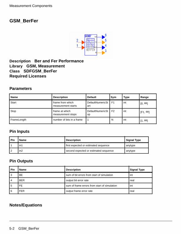
Measurement Components
GSM_BerFer
Description Ber and Fer PerformanceLibrary GSM, MeasurementClass SDFGSM_BerFerRequired Licenses
Parameters
Pin Inputs
Pin Outputs
Notes/Equations
Name Description Default Sym Type Range
Start frame from whichmeasurement starts
DefaultNumericStart
F1 int [0,∞]
Stop frame at whichmeasurement stops
DefaultNumericStop
F2 int [F1,∞]
FrameLength number of bits in a frame 1 N int [1,∞]
Pin Name Description Signal Type
1 in1 first expected or estimated sequence anytype
2 in2 second expected or estimated sequence anytype
Pin Name Description Signal Type
3 BE sum of bit errors from start of simulation int
4 BER output bit error rate real
5 FE sum of frame errors from start of simulation int
6 FER output frame error rate real
5-2 GSM_BerFer
1. This model is used to calculate system bit error rate (BER) and frame error rate(FER). One output token is produced for each N token consumed.
2. Implementation
The Monte Carlo method is used to calculate the BER and FER of the systemfrom the F1th frame to the F2th frame.
GSM_BerFer 5-3
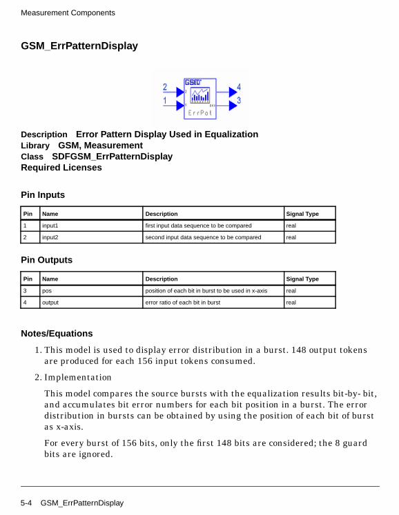
Measurement Components
GSM_ErrPatternDisplay
Description Error Pattern Display Used in EqualizationLibrary GSM, MeasurementClass SDFGSM_ErrPatternDisplayRequired Licenses
Pin Inputs
Pin Outputs
Notes/Equations
1. This model is used to display error distribution in a burst. 148 output tokensare produced for each 156 input tokens consumed.
2. Implementation
This model compares the source bursts with the equalization results bit-by- bit,and accumulates bit error numbers for each bit position in a burst. The errordistribution in bursts can be obtained by using the position of each bit of burstas x-axis.
For every burst of 156 bits, only the first 148 bits are considered; the 8 guardbits are ignored.
Pin Name Description Signal Type
1 input1 first input data sequence to be compared real
2 input2 second input data sequence to be compared real
Pin Name Description Signal Type
3 pos position of each bit in burst to be used in x-axis real
4 output error ratio of each bit in burst real
5-4 GSM_ErrPatternDisplay

Chapter 6: Modem Components
6-1
Modem Components
GSM_AQuarterBitAdd
Description Add 0.25-Bit to 156-Bit BurstLibrary GSM, ModemsClass SDFGSM_AQuarterBitAddRequired Licenses
Parameters
Pin Inputs
Pin Outputs
Notes/Equations
1. This model is used to add 0.25bit×M points that are set from 0 to a burst of 156bits of modulated signal in order to simulate a burst of 156.25 bits in a GSMsystem.
Name Description Default Type
SampleRate number of samples in onebit interval: SampleRate 4,SampleRate 8,SampleRate 16
SampleRate 16 enum
Pin Name Description Signal Type
1 st modulated signal with a burst of 156 bits complex
2 fi carrier frequency real
Pin Name Description Signal Type
3 sa modulated signal with a burst of 156.25 bits complex
4 fo carrier frequency real
6-2 GSM_AQuarterBitAdd
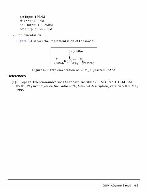
st: Input 156×Mfi: Input 156×Msa: Output 156.25×Mfo: Output 156.25×M
2. Implementation
Figure 6-1 shows the implementation of the model.
Figure 6-1. Implementation of GSM_AQuarterBitAdd
References
[1]European Telecommunications Standard Institute (ETSI), Rec. ETSI/GSM05.01, Physical layer on the radio path; General description, version 5.0.0, May1996.
time
adding
0 (0.25×M)
(156×M) (156.25×M)
st sa
GSM_AQuarterBitAdd 6-3
Modem Components
GSM_AQuarterBitRmv
Description Remove 0.25-Bit from 156.25-Bit BurstLibrary GSM, ModemsClass SDFGSM_AQuarterBitRmvRequired Licenses
Parameters
Pin Inputs
Pin Outputs
Notes/Equations
1. This model is used to remove 0.25-bit×M points in a burst of 156.25-bit×Mpoints of modulated signal. It is the reverse process of GSM_AQuarterBitAdd.After removal of the 0.25-bit, the signal will be sent to the demodulation modelfor demodulation.
Name Description Default Type
SampleRate number of samples in onebit interval: SampleRate 4,SampleRate 8,SampleRate 16
SampleRate 16 enum
Pin Name Description Signal Type
1 st modulated signal with a burst of 156.25 bits complex
2 fi carrier frequency real
Pin Name Description Signal Type
3 so modulated signal with a burst of 156 bits complex
4 fo carrier frequency real
6-4 GSM_AQuarterBitRmv
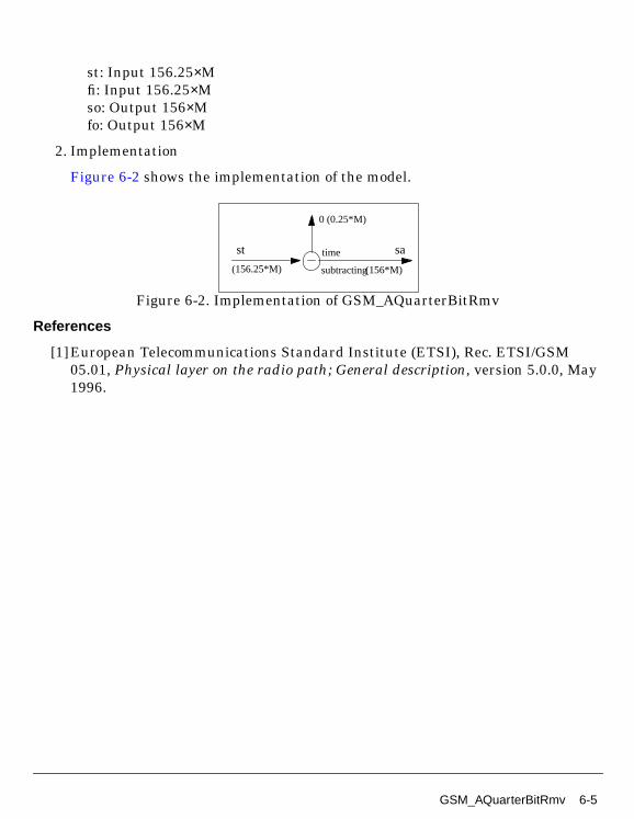
st: Input 156.25×Mfi: Input 156.25×Mso: Output 156×Mfo: Output 156×M
2. Implementation
Figure 6-2 shows the implementation of the model.
Figure 6-2. Implementation of GSM_AQuarterBitRmv
References
[1]European Telecommunications Standard Institute (ETSI), Rec. ETSI/GSM05.01, Physical layer on the radio path; General description, version 5.0.0, May1996.
time
subtracting
0 (0.25*M)
(156*M)(156.25*M)
st sa
GSM_AQuarterBitRmv 6-5
Modem Components
GSM_Carrier
Description Generation of Modulated SignalLibrary GSM, ModemsClass SDFGSM_CarrierRequired Licenses
Parameters
Pin Inputs
Pin Outputs
Notes/Equations
1. This model is used to generate modulated signal which is represented bycomplex envelope equivalent and carrier frequency. One token is consumed ateach input pin; one token is produced at each output pin.
2. Implementation
Name Description Default Unit Type Range
Fc carrier frequency 45e6 Hz real (0,∞)
Pc power per modulating bit 1e-3 W real (0,∞)
Pin Name Description Signal Type
1 Ii COS value of the modulated signal phase real
2 Qi SIN value of the modulated signal phase real
Pin Name Description Signal Type
3 It I branch of complex envelope of modulated signal real
4 Qt Q branch of complex envelope of modulated signal real
5 fo carrier frequency real
6-6 GSM_Carrier
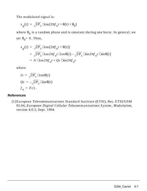
The modulated signal is:
where is a random phase and is constant during one burst. In general, we
set . Then,
where
.
References
[1]European Telecommunications Standard Institute (ETSI), Rec. ETSI/GSM05.04, European Digital Cellular Telecommunications System, Modulation,version 4.0.3, Sept. 1994.
xg t( ) 2Pc 2πf ot θ t( ) θ0+ +( )cos⋅=
θ0
θ0 0=
xg t( ) 2Pc 2πf ot θ t( )+( )cos⋅=
2Pc 2πf otcos θ t( )cos⋅ ⋅ 2Pc 2sin πf ot θsin t( )⋅ ⋅–=
It 2πf otcos⋅ Qt 2sin πf ot⋅+=
It 2Pc θ t( )cos⋅=
Qt 2Pc θsin t( )⋅–=
f o Fc1=
GSM_Carrier 6-7
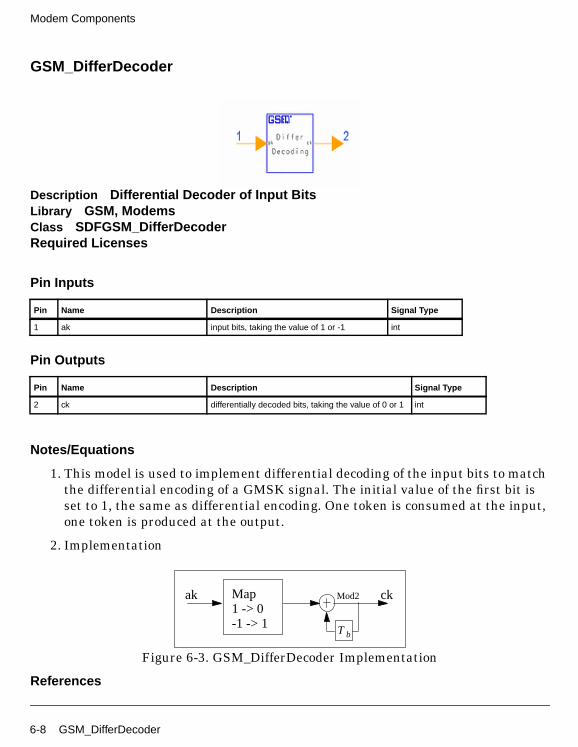
Modem Components
GSM_DifferDecoder
Description Differential Decoder of Input BitsLibrary GSM, ModemsClass SDFGSM_DifferDecoderRequired Licenses
Pin Inputs
Pin Outputs
Notes/Equations
1. This model is used to implement differential decoding of the input bits to matchthe differential encoding of a GMSK signal. The initial value of the first bit isset to 1, the same as differential encoding. One token is consumed at the input,one token is produced at the output.
2. Implementation
Figure 6-3. GSM_DifferDecoder Implementation
References
Pin Name Description Signal Type
1 ak input bits, taking the value of 1 or -1 int
Pin Name Description Signal Type
2 ck differentially decoded bits, taking the value of 0 or 1 int
Map1 -> 0-1 -> 1
Mod2
Tb
ak ck
6-8 GSM_DifferDecoder

[1]European Telecommunications Standard Institute (ETSI), Rec. ETSI/GSM05.04, European Digital Cellular Telecommunications System, Modulation,version 4.0.3, Sept. 1994.
GSM_DifferDecoder 6-9

Modem Components
GSM_DifferEncoder
Description Differential Encoder of Input BitsLibrary GSM, ModemsClass SDFGSM_DifferEncoderRequired Licenses
Pin Inputs
Pin Outputs
Notes/Equations
1. This model is used to implement differential encoding of the input bits, which isrequired in GSM standard to generate GMSK signal. According to the standardGSM 05.04, the initial value of the first bit is assigned to 1. One token isconsumed at the input, one token is produced at the output.
2. Implementation
Figure 6-4. GSM_DifferEncoder Implementation
References
Pin Name Description Signal Type
1 dk input bits, taking the value of 0 or 1 int
Pin Name Description Signal Type
2 ak differentially encoded bits, taking the value of 1 or -1 int
Mod2
Tb
dk Map0 -> 11 -> -1
ak
6-10 GSM_DifferEncoder
[1]European Telecommunications Standard Institute (ETSI), Rec. ETSI/GSM05.04, European Digital Cellular Telecommunications System, Modulation,version 4.0.3, Sept. 1994.
GSM_DifferEncoder 6-11
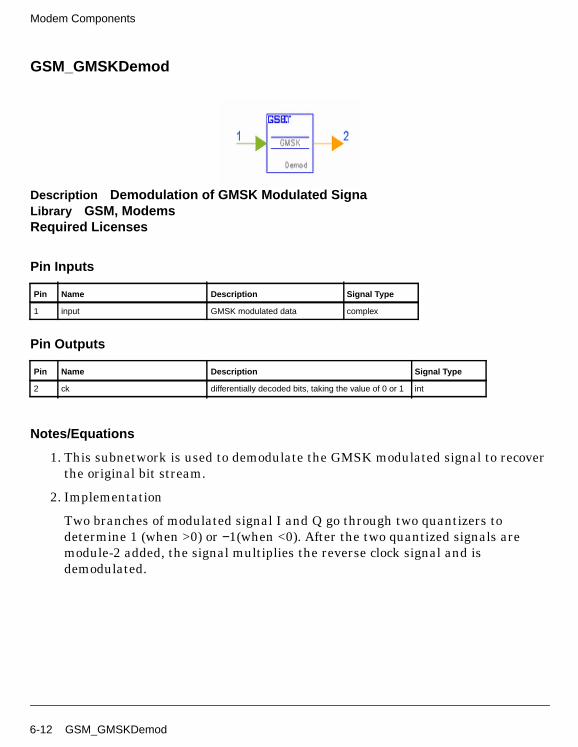
Modem Components
GSM_GMSKDemod
Description Demodulation of GMSK Modulated SignaLibrary GSM, ModemsRequired Licenses
Pin Inputs
Pin Outputs
Notes/Equations
1. This subnetwork is used to demodulate the GMSK modulated signal to recoverthe original bit stream.
2. Implementation
Two branches of modulated signal I and Q go through two quantizers todetermine 1 (when >0) or −1(when <0). After the two quantized signals aremodule-2 added, the signal multiplies the reverse clock signal and isdemodulated.
Pin Name Description Signal Type
1 input GMSK modulated data complex
Pin Name Description Signal Type
2 ck differentially decoded bits, taking the value of 0 or 1 int
6-12 GSM_GMSKDemod
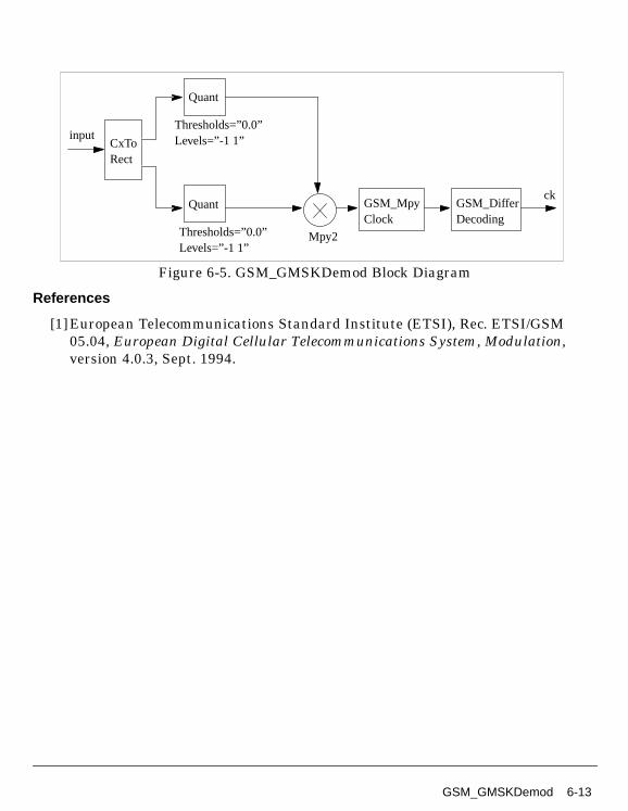
Figure 6-5. GSM_GMSKDemod Block Diagram
References
[1]European Telecommunications Standard Institute (ETSI), Rec. ETSI/GSM05.04, European Digital Cellular Telecommunications System, Modulation,version 4.0.3, Sept. 1994.
CxToRect
input
Quant
Quant
Thresholds=”0.0”Levels=”-1 1”
Thresholds=”0.0”Levels=”-1 1”
Mpy2
GSM_Mpy GSM_DifferDecodingClock
ck
GSM_GMSKDemod 6-13

Modem Components
GSM_GMSKMod
Description Generation of GMSK Modulated SignalLibrary GSM, ModemsRequired Licenses
Parameters
Pin Inputs
Pin Outputs
Notes/Equations
1. This subnetwork is used to generate a GMSK modulated signal that isrepresented by complex envelope equivalent and carrier frequency.
2. Implementation
Name Description Default Unit Type Range
SampleRate number of samples in onebit interval: SampleRate 4,SampleRate 8,SampleRate 16
SampleRate 16 enum
Fc carrier frequency 45e6 Hz real (0,∞)
Pc power per modulating bit 1e-3 W real (0,∞)
Pin Name Description Signal Type
1 dk input bits, value of 0 or 1 int
Pin Name Description Signal Type
2 output complex envelope of modulated signal complex
3 fo carrier frequency real
6-14 GSM_GMSKMod
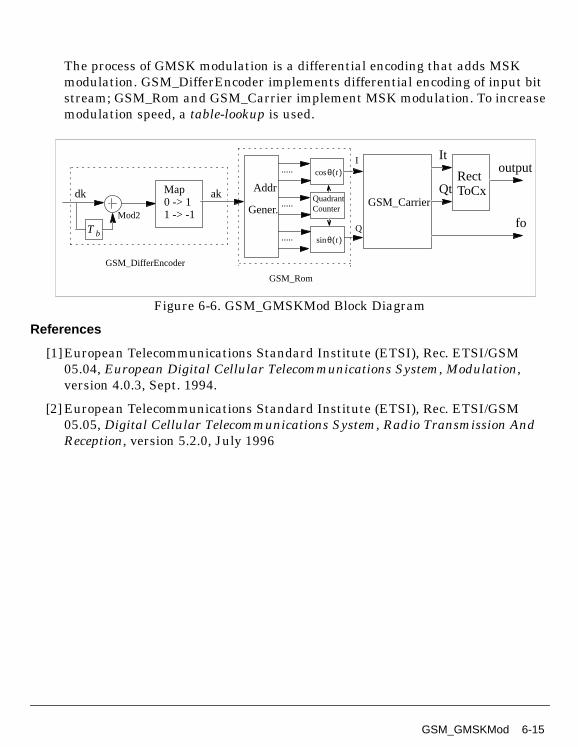
The process of GMSK modulation is a differential encoding that adds MSKmodulation. GSM_DifferEncoder implements differential encoding of input bitstream; GSM_Rom and GSM_Carrier implement MSK modulation. To increasemodulation speed, a table-lookup is used.
Figure 6-6. GSM_GMSKMod Block Diagram
References
[1]European Telecommunications Standard Institute (ETSI), Rec. ETSI/GSM05.04, European Digital Cellular Telecommunications System, Modulation,version 4.0.3, Sept. 1994.
[2] European Telecommunications Standard Institute (ETSI), Rec. ETSI/GSM05.05, Digital Cellular Telecommunications System, Radio Transmission AndReception, version 5.2.0, July 1996
Addr
.....
.....
.....
CounterQuadrant
Gener.Mod2
Tbθsin t( )
θ t( )cos
dk Map0 -> 11 -> -1
akGSM_Carrier
I
Q
RectToCx
It
fo
Qt
output
GSM_DifferEncoder
GSM_Rom
GSM_GMSKMod 6-15
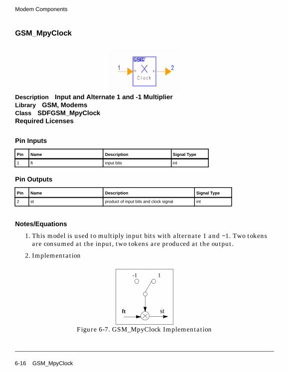
Modem Components
GSM_MpyClock
Description Input and Alternate 1 and -1 MultiplierLibrary GSM, ModemsClass SDFGSM_MpyClockRequired Licenses
Pin Inputs
Pin Outputs
Notes/Equations
1. This model is used to multiply input bits with alternate 1 and −1. Two tokensare consumed at the input, two tokens are produced at the output.
2. Implementation
Figure 6-7. GSM_MpyClock Implementation
Pin Name Description Signal Type
1 ft input bits int
Pin Name Description Signal Type
2 st product of input bits and clock signal int
1-1
ft st
6-16 GSM_MpyClock
The model implements input signal ft by multiplying it with a reverse clocksignal. Each firing, ft inputs 2 tokens, the first is to multiply 1, the second is tomultiply −1.
GSM_MpyClock 6-17
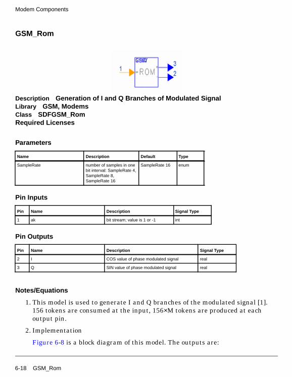
Modem Components
GSM_Rom
Description Generation of I and Q Branches of Modulated SignalLibrary GSM, ModemsClass SDFGSM_RomRequired Licenses
Parameters
Pin Inputs
Pin Outputs
Notes/Equations
1. This model is used to generate I and Q branches of the modulated signal [1].156 tokens are consumed at the input, 156×M tokens are produced at eachoutput pin.
2. Implementation
Figure 6-8 is a block diagram of this model. The outputs are:
Name Description Default Type
SampleRate number of samples in onebit interval: SampleRate 4,SampleRate 8,SampleRate 16
SampleRate 16 enum
Pin Name Description Signal Type
1 ak bit stream; value is 1 or -1 int
Pin Name Description Signal Type
2 I COS value of phase modulated signal real
3 Q SIN value of phase modulated signal real
6-18 GSM_Rom
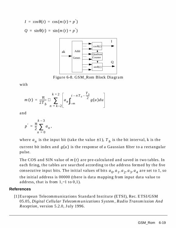
Figure 6-8. GSM_Rom Block Diagram
with
and
,
where is the input bit (take the value ), is the bit interval, k is the
current bit index and is the response of a Gaussian filter to a rectangularpulse.
The COS and SIN value of are pre-calculated and saved in two tables. Ineach firing, the tables are searched according to the address formed by the fiveconsecutive input bits. The initial values of bits are set to 1, so
the initial address is 00000 (there is data mapping from input data value toaddress, that is from 1,−1 to 0,1).
References
[1]European Telecommunications Standard Institute (ETSI), Rec. ETSI/GSM05.05, Digital Cellular Telecommunications System, Radio Transmission AndReception, version 5.2.0, July 1996.
I θ t( )cos m t( ) p ′+( )cos= =
Q θsin t( ) m t( ) p ′+( )sin= =
Addr
.....
.....
.....
CounterQuadrant
Gener.
θsin t( )
θ t( )cos
ak
I
Q
m t( ) π2Tb---------- an g u( ) ud
∞–
t nTb–Tb
2------–
∫n k 2–=
k 2+
∑⋅=
p ′ π2--- an
n 0=
k 3–
∑=
an 1± Tb
g u( )
m t( )
a0 a1 a2 a3 a4, , , ,
GSM_Rom 6-19

Modem Components
6-20

Chapter 7: Speech Codec Components
7-1
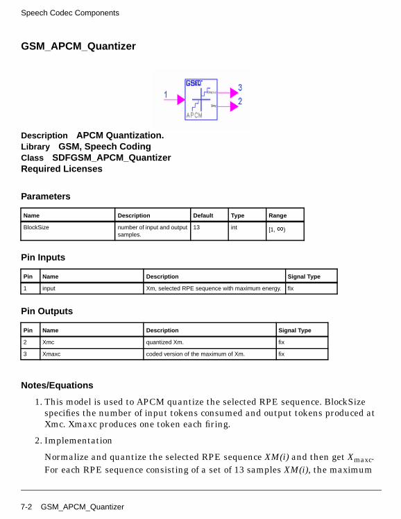
Speech Codec Components
GSM_APCM_Quantizer
Description APCM Quantization.Library GSM, Speech CodingClass SDFGSM_APCM_QuantizerRequired Licenses
Parameters
Pin Inputs
Pin Outputs
Notes/Equations
1. This model is used to APCM quantize the selected RPE sequence. BlockSizespecifies the number of input tokens consumed and output tokens produced atXmc. Xmaxc produces one token each firing.
2. Implementation
Normalize and quantize the selected RPE sequence XM(i) and then get Xmaxc.For each RPE sequence consisting of a set of 13 samples XM(i), the maximum
Name Description Default Type Range
BlockSize number of input and outputsamples.
13 int [1,∞)
Pin Name Description Signal Type
1 input Xm, selected RPE sequence with maximum energy. fix
Pin Name Description Signal Type
2 Xmc quantized Xm. fix
3 Xmaxc coded version of the maximum of Xm. fix
7-2 GSM_APCM_Quantizer
Xmax of the absolute values XM(i) is selected and quantized logarithmicallywith 6 bits Xmaxc (as given in table 3.5 of GSM 06.10 section 3.1.20).
For normalization, the 13 samples are divided by the decoded version X'max of
the block maximum: . The normalized samples
X'(i) are quantized uniformly with three bits to obtain XMc(i).
References
[1]European Telecommunications Standard Institute (ETSI), Rec. ETSI/GSM06.10, Full Rate Speech Transcoding, version 4.0.2, Sept. 1994.
[2] GSM_InverseAPCM model.
X ' i( ) X M i( ) X 'max⁄ ;i=0,,12=
GSM_APCM_Quantizer 7-3
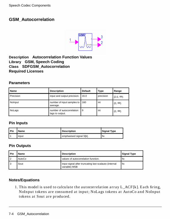
Speech Codec Components
GSM_Autocorrelation
Description Autocorrelation Function ValuesLibrary GSM, Speech CodingClass SDFGSM_AutocorrelationRequired Licenses
Parameters
Pin Inputs
Pin Outputs
Notes/Equations
1. This model is used to calculate the autocorrelation array L_ACF[k]. Each firing,NoInput tokens are consumed at input; NoLags tokens at AutoCo and NoInputtokens at Sout are produced.
Name Description Default Type Range
Precision input and output precision. 16.0 precision [2.0,∞)
NoInput number of input samples toaverage.
160 int (0,∞)
NoLags number of autocorrelationlags to output.
9 int (0,∞)
Pin Name Description Signal Type
1 input emphasised signal S[k]. fix
Pin Name Description Signal Type
2 AutoCo values of autocorrelation function. fix
3 Sout input signal after truncating last scalauto (internalvariable) MSB
fix
7-4 GSM_Autocorrelation
2. Implementation
References
[1]European Telecommunications Standard Institute (ETSI), Rec. ETSI/GSM06.10, Full Rate Speech Transcoding, version 4.0.2, Sept. 1994.
ACF k( ) S i( ) S i k–( )×i k=
159
∑=
k 0 1 … 8, , ,=
GSM_Autocorrelation 7-5
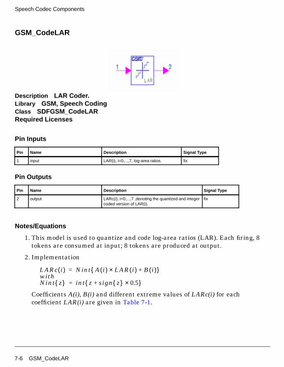
Speech Codec Components
GSM_CodeLAR
Description LAR Coder.Library GSM, Speech CodingClass SDFGSM_CodeLARRequired Licenses
Pin Inputs
Pin Outputs
Notes/Equations
1. This model is used to quantize and code log-area ratios (LAR). Each firing, 8tokens are consumed at input; 8 tokens are produced at output.
2. Implementation
Coefficients A(i), B(i) and different extreme values of LARc(i) for eachcoefficient LAR(i) are given in Table 7-1.
Pin Name Description Signal Type
1 input LAR(i), i=0,...,7, log-area ratios. fix
Pin Name Description Signal Type
2 output LARc(i), i=0,...,7 ,denoting the quantized and integercoded version of LAR(i).
fix
LARc i( ) Nint A i( ) LAR i( ) B i( )+×{ }withNint z{ } int z sign z{ } 0.5×+{ }
=
=
7-6 GSM_CodeLAR
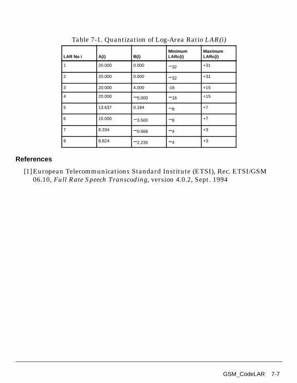
References
[1]European Telecommunications Standard Institute (ETSI), Rec. ETSI/GSM06.10, Full Rate Speech Transcoding, version 4.0.2, Sept. 1994
Table 7-1. Quantization of Log-Area Ratio LAR(i)
LAR No i A(i) B(i)MinimumLARc(i)
MaximumLARc(i)
1 20.000 0.000 −32 +31
2 20.000 0.000 −32 +31
3 20.000 4.000 -16 +15
4 20.000 −5.000 −16 +15
5 13.637 0.184 −8 +7
6 15.000 −3.500 −8 +7
7 8.334 −0.666 −4 +3
8 8.824 −2.235 −4 +3
GSM_CodeLAR 7-7

Speech Codec Components
GSM_DecodeLAR
Description LAR DecoderLibrary GSM, Speech CodingClass SDFGSM_DecodeLARRequired Licenses
Pin Inputs
Pin Outputs
Notes/Equations
1. This model is used to decode LARc. Input LARc(i), i = 0, ... , 7, are coded in 6, 6,5, 5, 4, 4, 3, 3 bits, respectively; the input tokens cannot exceed their extremevalues. Each firing, 8 tokens are consumed at input, and 8 tokens are producedat output.
2. Implementation
Coefficients A(i), B(i) and different extreme values of LARc(i) for eachcoefficient LAR(i) are given in Table 7-2.
Pin Name Description Signal Type
1 input LARc(i), i=0,...,7, quantized and integer codedversion of LAR(i).
fix
Pin Name Description Signal Type
2 output LAR’’(i), i=0,...,7 , decoded LARc(i). fix
LAR'' i( ) LARc i( ) B i( )–( ) A i( )⁄=
7-8 GSM_DecodeLAR
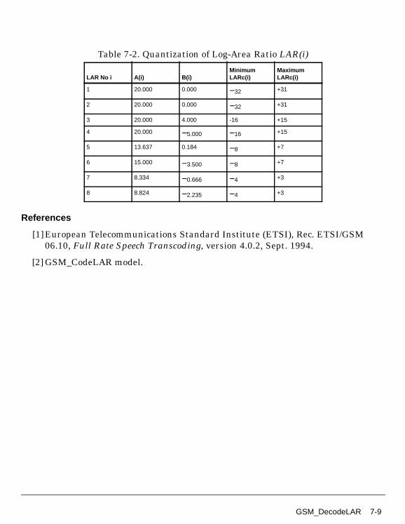
References
[1]European Telecommunications Standard Institute (ETSI), Rec. ETSI/GSM06.10, Full Rate Speech Transcoding, version 4.0.2, Sept. 1994.
[2] GSM_CodeLAR model.
Table 7-2. Quantization of Log-Area Ratio LAR(i)
LAR No i A(i) B(i)MinimumLARc(i)
MaximumLARc(i)
1 20.000 0.000 −32 +31
2 20.000 0.000 −32 +31
3 20.000 4.000 -16 +15
4 20.000 −5.000 −16 +15
5 13.637 0.184 −8 +7
6 15.000 −3.500 −8 +7
7 8.334 −0.666 −4 +3
8 8.824 −2.235 −4 +3
GSM_DecodeLAR 7-9
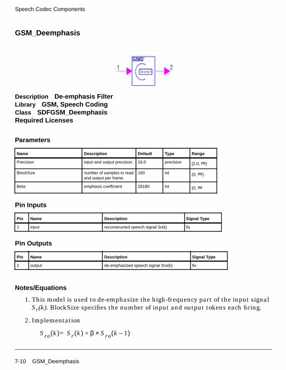
Speech Codec Components
GSM_Deemphasis
Description De-emphasis FilterLibrary GSM, Speech CodingClass SDFGSM_DeemphasisRequired Licenses
Parameters
Pin Inputs
Pin Outputs
Notes/Equations
1. This model is used to de-emphasize the high-frequency part of the input signalSr(k). BlockSize specifies the number of input and output tokens each firing.
2. Implementation
Name Description Default Type Range
Precision input and output precision. 16.0 precision [2.0,∞)
BlockSize number of samples to readand output per frame.
160 int (0,∞)
Beta emphasis coefficient 28180 int (0,∞
Pin Name Description Signal Type
1 input reconstructed speech signal Sr(k) fix
Pin Name Description Signal Type
2 output de-emphasized speech signal Sro(k) fix
Sro k( ) Sr k( ) β Sro× k 1–( )+=
7-10 GSM_Deemphasis

where β is the emphasis coefficient.
References
[1]European Telecommunications Standard Institute (ETSI), Rec. ETSI/GSM06.10, Full Rate Speech Transcoding, version 4.0.2, Sept. 1994
[2] GSM_Preemphasis model.
GSM_Deemphasis 7-11
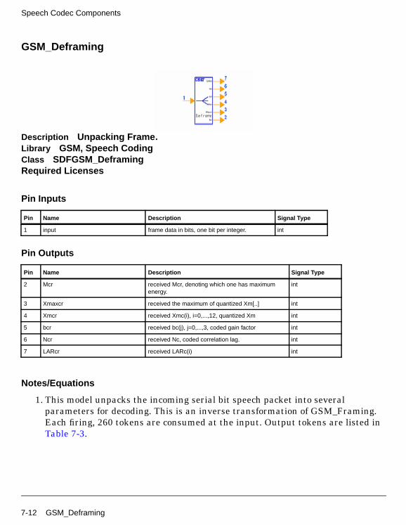
Speech Codec Components
GSM_Deframing
Description Unpacking Frame.Library GSM, Speech CodingClass SDFGSM_DeframingRequired Licenses
Pin Inputs
Pin Outputs
Notes/Equations
1. This model unpacks the incoming serial bit speech packet into severalparameters for decoding. This is an inverse transformation of GSM_Framing.Each firing, 260 tokens are consumed at the input. Output tokens are listed inTable 7-3.
Pin Name Description Signal Type
1 input frame data in bits, one bit per integer. int
Pin Name Description Signal Type
2 Mcr received Mcr, denoting which one has maximumenergy.
int
3 Xmaxcr received the maximum of quantized Xm[..] int
4 Xmcr received Xmc(i), i=0,...,12, quantized Xm int
5 bcr received bc(j), j=0,...,3, coded gain factor int
6 Ncr received Nc, coded correlation lag. int
7 LARcr received LARc(i) int
7-12 GSM_Deframing

References
[1]European Telecommunications Standard Institute (ETSI), Rec. ETSI/GSM06.10, Full Rate Speech Transcoding, version 4.0.2, Sept. 1994.
[2] GSM_Framing model.
Table 7-3. Output Tokens
Output Pin Output Tokens
Mcr 4
Xmaxcr 4
Xmcr 13 × 4
bcr 4
Ncr 4
LARcr 8
GSM_Deframing 7-13
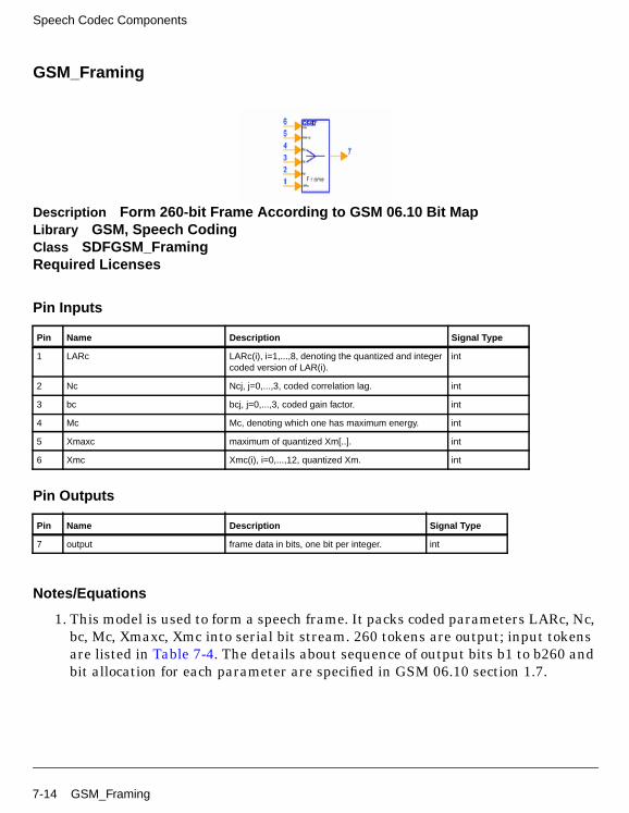
Speech Codec Components
GSM_Framing
Description Form 260-bit Frame According to GSM 06.10 Bit MapLibrary GSM, Speech CodingClass SDFGSM_FramingRequired Licenses
Pin Inputs
Pin Outputs
Notes/Equations
1. This model is used to form a speech frame. It packs coded parameters LARc, Nc,bc, Mc, Xmaxc, Xmc into serial bit stream. 260 tokens are output; input tokensare listed in Table 7-4. The details about sequence of output bits b1 to b260 andbit allocation for each parameter are specified in GSM 06.10 section 1.7.
Pin Name Description Signal Type
1 LARc LARc(i), i=1,...,8, denoting the quantized and integercoded version of LAR(i).
int
2 Nc Ncj, j=0,...,3, coded correlation lag. int
3 bc bcj, j=0,...,3, coded gain factor. int
4 Mc Mc, denoting which one has maximum energy. int
5 Xmaxc maximum of quantized Xm[..]. int
6 Xmc Xmc(i), i=0,...,12, quantized Xm. int
Pin Name Description Signal Type
7 output frame data in bits, one bit per integer. int
7-14 GSM_Framing

References
[1]European Telecommunications Standard Institute (ETSI), Rec. ETSI/GSM06.10, Full Rate Speech Transcoding, version 4.0.2, Sept. 1994.
[2] GSM_Deframing model.
Table 7-4. Input Tokens
Input Pin Input Tokens
Mcr 4
Xmaxcr 4
Xmcr 13 × 4
bcr 4
Ncr 4
LARcr 8
GSM_Framing 7-15
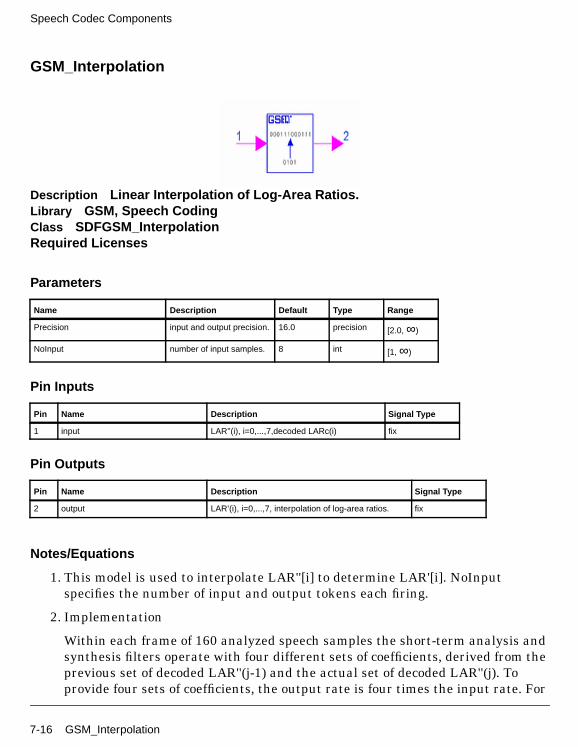
Speech Codec Components
GSM_Interpolation
Description Linear Interpolation of Log-Area Ratios.Library GSM, Speech CodingClass SDFGSM_InterpolationRequired Licenses
Parameters
Pin Inputs
Pin Outputs
Notes/Equations
1. This model is used to interpolate LAR''[i] to determine LAR'[i]. NoInputspecifies the number of input and output tokens each firing.
2. Implementation
Within each frame of 160 analyzed speech samples the short-term analysis andsynthesis filters operate with four different sets of coefficients, derived from theprevious set of decoded LAR''(j-1) and the actual set of decoded LAR''(j). Toprovide four sets of coefficients, the output rate is four times the input rate. For
Name Description Default Type Range
Precision input and output precision. 16.0 precision [2.0,∞)
NoInput number of input samples. 8 int [1,∞)
Pin Name Description Signal Type
1 input LAR’’(i), i=0,...,7,decoded LARc(i) fix
Pin Name Description Signal Type
2 output LAR’(i), i=0,...,7, interpolation of log-area ratios. fix
7-16 GSM_Interpolation
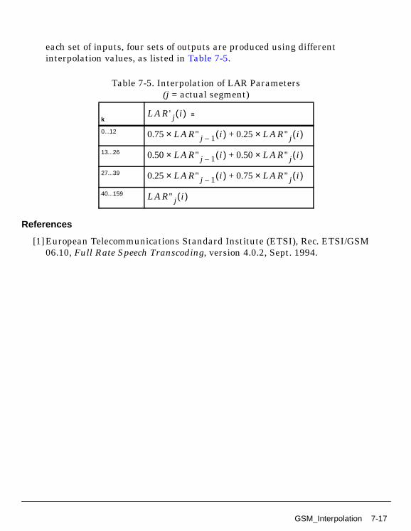
each set of inputs, four sets of outputs are produced using differentinterpolation values, as listed in Table 7-5.
References
[1]European Telecommunications Standard Institute (ETSI), Rec. ETSI/GSM06.10, Full Rate Speech Transcoding, version 4.0.2, Sept. 1994.
Table 7-5. Interpolation of LAR Parameters(j = actual segment)
k =
0...12
13...26
27...39
40...159
LAR' j i( )
0.75 LAR'' j 1– i( )× 0.25 LAR'' j i( )×+
0.50 LAR'' j 1– i( )× 0.50 LAR'' j i( )×+
0.25 LAR'' j 1– i( )× 0.75 LAR'' j i( )×+
LAR'' j i( )
GSM_Interpolation 7-17

Speech Codec Components
GSM_InverseAPCM
Description APCM DecodeLibrary GSM, Speech CodingClass SDFGSM_InverseAPCMRequired Licenses
Parameters
Pin Inputs
Pin Outputs
Notes/Equations
1. This model is used to decode the coded RPE sequence. BlockSize specifies thenumber of tokens consumed at Xmc and produced at output. Xmaxc consumesone token each firing.
2. Implementation
Name Description Default Type Range
BlockSize number of input and outputsamples.
13 int [1,∞)
Pin Name Description Signal Type
1 Xmc quantized Xm fix
2 Xmaxc coded version of the maximum of Xm fix
Pin Name Description Signal Type
3 output reconstructed X’m(i). fix
7-18 GSM_InverseAPCM

This is an inverse transformation of GSM_APCM_Quantizer. After decodingof , a denormalizing process is used to obtain the reconstructed
sub-sequence .
References
[1]European Telecommunications Standard Institute (ETSI), Rec. ETSI/GSM06.10, Full Rate Speech Transcoding, version 4.0.2, Sept. 1994.
X ′maxc X Mc i( )
X 'M i( )
GSM_InverseAPCM 7-19
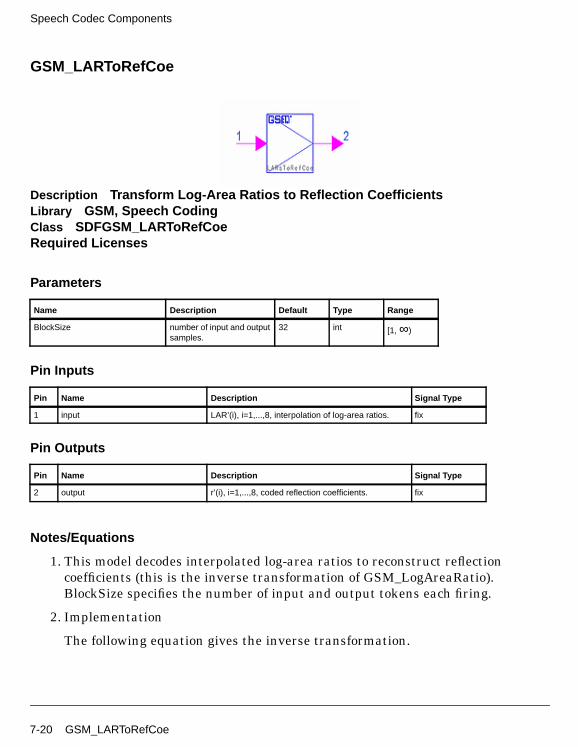
Speech Codec Components
GSM_LARToRefCoe
Description Transform Log-Area Ratios to Reflection CoefficientsLibrary GSM, Speech CodingClass SDFGSM_LARToRefCoeRequired Licenses
Parameters
Pin Inputs
Pin Outputs
Notes/Equations
1. This model decodes interpolated log-area ratios to reconstruct reflectioncoefficients (this is the inverse transformation of GSM_LogAreaRatio).BlockSize specifies the number of input and output tokens each firing.
2. Implementation
The following equation gives the inverse transformation.
Name Description Default Type Range
BlockSize number of input and outputsamples.
32 int [1,∞)
Pin Name Description Signal Type
1 input LAR’(i), i=1,...,8, interpolation of log-area ratios. fix
Pin Name Description Signal Type
2 output r’(i), i=1,...,8, coded reflection coefficients. fix
7-20 GSM_LARToRefCoe
References
[1]European Telecommunications Standard Institute (ETSI), Rec. ETSI/GSM06.10, Full Rate Speech Transcoding, version 4.0.2, Sept. 1994.
r' i( )LAR' i( ) LAR' i( ) 0.675<;
sign LAR' i( )[ ] 0.500 LAR' i( )× 0.337500+[ ] 0.675 LAR' i( )≤ 1.225<;×sign LAR' i( )[ ] 0.125 LAR' i( )× 0.796875+[ ]× 1.225 LAR' i( )≤ 1.625≤;
=
GSM_LARToRefCoe 7-21
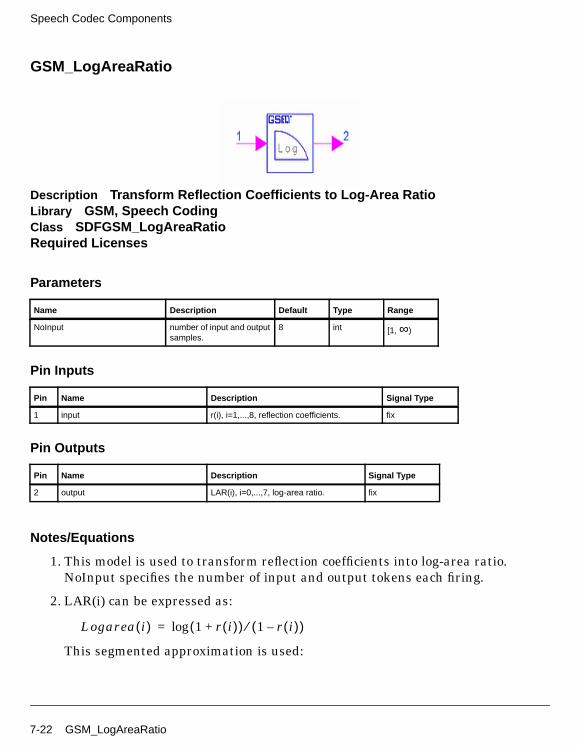
Speech Codec Components
GSM_LogAreaRatio
Description Transform Reflection Coefficients to Log-Area RatioLibrary GSM, Speech CodingClass SDFGSM_LogAreaRatioRequired Licenses
Parameters
Pin Inputs
Pin Outputs
Notes/Equations
1. This model is used to transform reflection coefficients into log-area ratio.NoInput specifies the number of input and output tokens each firing.
2. LAR(i) can be expressed as:
This segmented approximation is used:
Name Description Default Type Range
NoInput number of input and outputsamples.
8 int [1,∞)
Pin Name Description Signal Type
1 input r(i), i=1,...,8, reflection coefficients. fix
Pin Name Description Signal Type
2 output LAR(i), i=0,...,7, log-area ratio. fix
Logarea i( ) 1 r i( )+( ) 1 r i( )–( )⁄log=
7-22 GSM_LogAreaRatio

The following scaling for r[..] and LAR[..] has been used:
r[..] = integer ( real_r[..] *32768); with −1 ≤ real_r < 1 LAR[..] = integer(real_LAR[..] * 16384); with −1.625 ≤ real_LAR[..] ≤ 1.625.
References
[1]European Telecommunications Standard Institute (ETSI), Rec. ETSI/GSM06.10, Full Rate Speech Transcoding, version 4.0.2, Sept. 1994.
[2] GSM_LARToRefCoe model.
LAR i( )r i( ) r i( ) 0.675<( );
sign r i( )[ ] 2 r i( )× 0.675–[ ] 0.675 r i( ) 0.950<≤;×sign r i( )[ ] 8 r i( )× 6.375–[ ] 0.950 r i( ) 1.000≤ ≤;×
=
GSM_LogAreaRatio 7-23
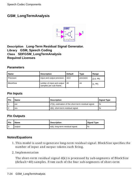
Speech Codec Components
GSM_LongTermAnalysis
Description Long-Term Residual Signal Generator.Library GSM, Speech CodingClass SDFGSM_LongTermAnalysisRequired Licenses
Parameters
Pin Inputs
Pin Outputs
Notes/Equations
1. This model is used to generate long-term residual signal. BlockSize specifies thenumber of input and output tokens each firing.
2. Implementation
The short-term residual signal d(k) is processed by sub-segments of BlockSize(default=40) samples. From each of the four sub-segments of short-term
Name Description Default Type Range
Precision input and output precision. 16.0 precision [2.0,∞)
BlockSize iumber of input and outputsamples per sub-frame.
40 int [1,∞)
Pin Name Description Signal Type
1 est d’’(k), estimation of the short-term residual signal. fix
2 res d(k), short-term residual signal. fix
Pin Name Description Signal Type
3 output e(k), long-term residual signal. fix
7-24 GSM_LongTermAnalysis
residual d(k), an estimate d''(k) of the signal is subtracted to generate thelong-term residual signal e(k).
References
[1]European Telecommunications Standard Institute (ETSI), Rec. ETSI/GSM06.10, Full Rate Speech Transcoding, version 4.0.2, Sept. 1994.
[2] GSM_LongTermSynthesis model.
e k j k+( ) d k j k+( ) d'' k j k+( )
j 0 … 3, ,=
k 0 …39,=
k j k0 j 40×+=
;–=
GSM_LongTermAnalysis 7-25
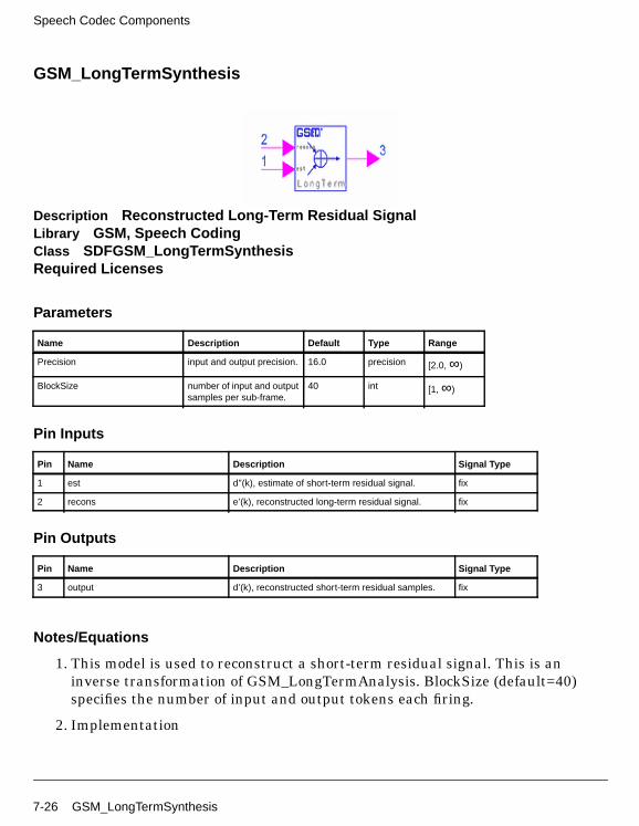
Speech Codec Components
GSM_LongTermSynthesis
Description Reconstructed Long-Term Residual SignalLibrary GSM, Speech CodingClass SDFGSM_LongTermSynthesisRequired Licenses
Parameters
Pin Inputs
Pin Outputs
Notes/Equations
1. This model is used to reconstruct a short-term residual signal. This is aninverse transformation of GSM_LongTermAnalysis. BlockSize (default=40)specifies the number of input and output tokens each firing.
2. Implementation
Name Description Default Type Range
Precision input and output precision. 16.0 precision [2.0,∞)
BlockSize number of input and outputsamples per sub-frame.
40 int [1,∞)
Pin Name Description Signal Type
1 est d’’(k), estimate of short-term residual signal. fix
2 recons e’(k), reconstructed long-term residual signal. fix
Pin Name Description Signal Type
3 output d’(k), reconstructed short-term residual samples. fix
7-26 GSM_LongTermSynthesis
This model adds the reconstructed long-term residual signal e'[0..39] to theestimated signal d''[0..39] from the long-term analysis filter to calculate thereconstructed short-term residual signal d'[0..39] (for next sub-frame).
References
[1]European Telecommunications Standard Institute (ETSI), Rec. ETSI/GSM06.10, Full Rate Speech Transcoding, version 4.0.2, Sept. 1994.
[2] GSM_LongTermAnalysis model.
d' k j k+( ) e' k j k+( ) d'' k j k+( )
j 0 … 3, ,=
k 0 …39,=
k j k0 j 40×+=
;+=
GSM_LongTermSynthesis 7-27
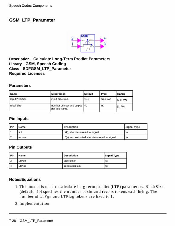
Speech Codec Components
GSM_LTP_Parameter
Description Calculate Long-Term Predict Parameters.Library GSM, Speech CodingClass SDFGSM_LTP_ParameterRequired Licenses
Parameters
Pin Inputs
Pin Outputs
Notes/Equations
1. This model is used to calculate long-term predict (LTP) parameters. BlockSize(default=40) specifies the number of sht and recons tokens each firing. Thenumber of LTPgn and LTPlag tokens are fixed to 1.
2. Implementation
Name Description Default Type Range
InputPrecision input precision. 16.0 precision [2.0,∞)
BlockSize number of input and outputper sub-frame.
40 int [1,∞)
Pin Name Description Signal Type
1 sht d(k), short-term residual signal. fix
2 recons d’(k), reconstructed short-term residual signal. fix
Pin Name Description Signal Type
3 LTPgn gain factor. fix
4 LTPlag correlation lag. fix
7-28 GSM_LTP_Parameter
• divide each 20 msec frame into four subsegments
• calculate a long-term correlation lag and an associated gain factor , j =
0, ... , 3 for four sub-segments
• encode LTP lags
• encode LTP gains bj
References
[1]European Telecommunications Standard Institute (ETSI), Rec. ETSI/GSM06.10, Full Rate Speech Transcoding, version 4.0.2, Sept. 1994.
[2] GSM_ShortTermPredict model.
N j b j
N j
GSM_LTP_Parameter 7-29
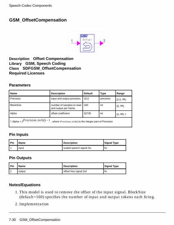
Speech Codec Components
GSM_OffsetCompensation
Description Offset CompensationLibrary GSM, Speech CodingClass SDFGSM_OffsetCompensationRequired Licenses
Parameters
Pin Inputs
Pin Outputs
Notes/Equations
1. This model is used to remove the offset of the input signal. BlockSize(default=160) specifies the number of input and output tokens each firing.
2. Implementation
Name Description Default Type Range
Precision input and output precision. 16.0 precision [2.0,∞)
BlockSize number of samples to readand output per frame.
160 int (0,∞)
Alpha offset coefficient 32735 int (0,∞) †
† Alpha = 2Precision.intb() - 1 , where Precision.intb() is the integer part of Precision
Pin Name Description Signal Type
1 input scaled speech signal So. fix
Pin Name Description Signal Type
2 output offset free signal Sof fix
7-30 GSM_OffsetCompensation

This component implements a highpass filter and requires extended arithmeticfor the recursive part of the filter (refer to 4.2.2 in GSM 06.10 for details).
References
[1]European Telecommunications Standard Institute (ETSI), Rec. ETSI/GSM06.10, Full Rate Speech Transcoding, version 4.0.2, Sept. 1994.
Sof k( ) So k( ) So k 1–( )– α Sof k 1–( )×
α
+
32735 215–×
=
=
GSM_OffsetCompensation 7-31

Speech Codec Components
GSM_Postprocessing
Description Post Processing.Library GSM, Speech CodingClass SDFGSM_PostprocessingRequired Licenses
Parameters
Pin Inputs
Pin Outputs
Notes/Equations
1. This model is used to upscale reconstructed uniform PCM 13-bit stream.BlockSize (default 160) specifies the number of input and output tokens eachfiring.
2. Implementation
• upscale the input signal.
• truncate the most right three bits of the upscaled signal.
Name Description Default Type Range
Precision input and output precision. 16.0 precision [2.0,∞)
BlockSize number of samples to readand output per frame.
160 int (0,∞)
Pin Name Description Signal Type
1 input reconstructed speech signal. fix
Pin Name Description Signal Type
2 output reconstructed speech signal after postprocessing. fix
7-32 GSM_Postprocessing

The output has the following format:
s.v.v.v.v.v.v.v.v.v.v.v.v.x.x.x (twos complement format)
where s is the sign bit, v is a valid bit, and x means don’t care.
References
[1]European Telecommunications Standard Institute (ETSI), Rec. ETSI/GSM06.10, Full Rate Speech Transcoding, version 4.0.2, Sept. 1994.
GSM_Postprocessing 7-33
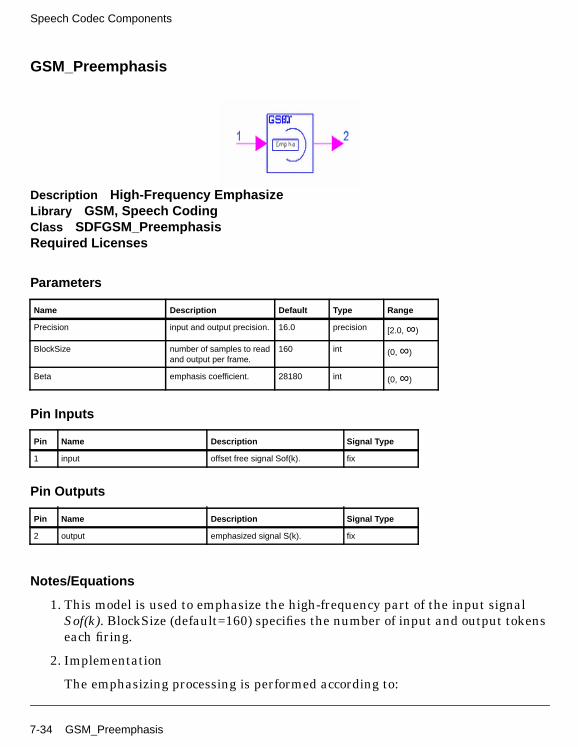
Speech Codec Components
GSM_Preemphasis
Description High-Frequency EmphasizeLibrary GSM, Speech CodingClass SDFGSM_PreemphasisRequired Licenses
Parameters
Pin Inputs
Pin Outputs
Notes/Equations
1. This model is used to emphasize the high-frequency part of the input signalSof(k). BlockSize (default=160) specifies the number of input and output tokenseach firing.
2. Implementation
The emphasizing processing is performed according to:
Name Description Default Type Range
Precision input and output precision. 16.0 precision [2.0,∞)
BlockSize number of samples to readand output per frame.
160 int (0,∞)
Beta emphasis coefficient. 28180 int (0,∞)
Pin Name Description Signal Type
1 input offset free signal Sof(k). fix
Pin Name Description Signal Type
2 output emphasized signal S(k). fix
7-34 GSM_Preemphasis
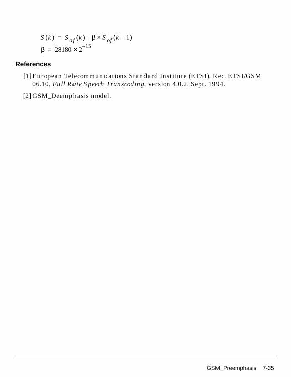
References
[1]European Telecommunications Standard Institute (ETSI), Rec. ETSI/GSM06.10, Full Rate Speech Transcoding, version 4.0.2, Sept. 1994.
[2] GSM_Deemphasis model.
S k( ) Sof k( ) β Sof k 1–( )×
β
–
28180 215–×
=
=
GSM_Preemphasis 7-35
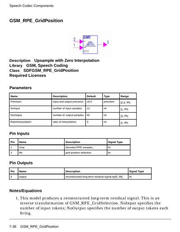
Speech Codec Components
GSM_RPE_GridPosition
Description Upsample with Zero InterpolationLibrary GSM, Speech CodingClass SDFGSM_RPE_GridPositionRequired Licenses
Parameters
Pin Inputs
Pin Outputs
Notes/Equations
1. This model produces a reconstructed long-term residual signal. This is aninverse transformation of GSM_RPE_GridSelection. NoInput specifies thenumber of input tokens; NoOutput specifies the number of output tokens eachfiring.
Name Description Default Type Range
Precision input and output precision. 16.0 precision [2.0,∞)
NoInput number of input samples. 13 int [1,∞)
NoOutput number of output samples. 40 int [3,∞)
RatioInterpolation ratio of interpolation. 3 int [1,∞)
Pin Name Description Signal Type
1 Xmp decoded RPE samples. fix
2 Mc grid position selection. fix
Pin Name Description Signal Type
3 output reconstructed long-term residual signal ep[0..39]. fix
7-36 GSM_RPE_GridPosition
2. Implementation
This model calculates the reconstructed long-term residual signal ep[0..39] forthe LTP analysis filter. Input Xmp[0..12] is upsampled by a factor of
RatioInterpolation by inserting zero values. Input Mc indicates theinterpolation phase.
References
[1]European Telecommunications Standard Institute (ETSI), Rec. ETSI/GSM06.10, Full Rate Speech Transcoding, version 4.0.2, Sept. 1994.
[2] GSM_RPE_GridSelection model.
GSM_RPE_GridPosition 7-37
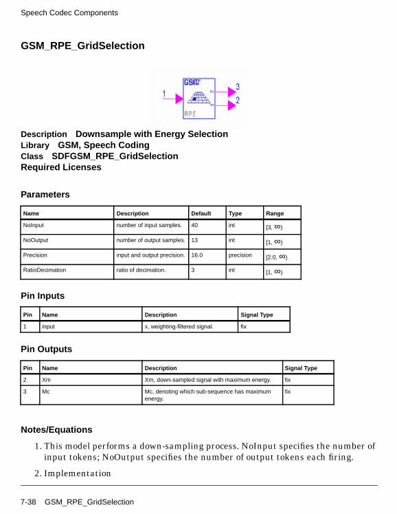
Speech Codec Components
GSM_RPE_GridSelection
Description Downsample with Energy SelectionLibrary GSM, Speech CodingClass SDFGSM_RPE_GridSelectionRequired Licenses
Parameters
Pin Inputs
Pin Outputs
Notes/Equations
1. This model performs a down-sampling process. NoInput specifies the number ofinput tokens; NoOutput specifies the number of output tokens each firing.
2. Implementation
Name Description Default Type Range
NoInput number of input samples. 40 int [3,∞)
NoOutput number of output samples. 13 int [1,∞)
Precision input and output precision. 16.0 precision [2.0,∞)
RatioDecimation ratio of decimation. 3 int [1,∞)
Pin Name Description Signal Type
1 input x, weighting-filtered signal. fix
Pin Name Description Signal Type
2 Xm Xm, down-sampled signal with maximum energy. fix
3 Mc Mc, denoting which sub-sequence has maximumenergy.
fix
7-38 GSM_RPE_GridSelection

The weighting-filtered signal x is down-sampled by a ratio of 3, and 4sub-sequences are provided.
where m denotes the position of the decimation grid.
The optimum candidate sub-sequence is selected, which is the one with
maximum energy.
The optimum grid position M is coded as Mc with 2 bits.
In this model, down-sampling ratio is a parameter. It should be in accordancewith:
NoOutput = int[NoInput/RatioDecimation]
where
int[x] indicates the largest integer ≤ x.
Output Xm(i) can be expressed as:
Xm(i) = x(m + RatioDecimation * i)
where
i = 0, ... , NoInput−1m = 0, ... , RatioDecimation + mod(NoInput/NoOutput).
References
[1]European Telecommunications Standard Institute (ETSI), Rec. ETSI/GSM06.10, Full Rate Speech Transcoding, version 4.0.2, Sept. 1994.
[2] GSM_RPE_GridPosition model.
xm
xm i( ) x k j m 3 i×+ +( )i 0 …12,=
m 0 … 3, ,=;=
X M
EM max xm2 i( ) m;
i 0=
12
∑ 0 … 3, ,= =
GSM_RPE_GridSelection 7-39
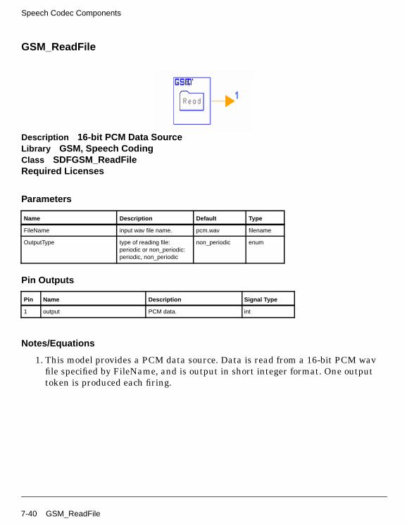
Speech Codec Components
GSM_ReadFile
Description 16-bit PCM Data SourceLibrary GSM, Speech CodingClass SDFGSM_ReadFileRequired Licenses
Parameters
Pin Outputs
Notes/Equations
1. This model provides a PCM data source. Data is read from a 16-bit PCM wavfile specified by FileName, and is output in short integer format. One outputtoken is produced each firing.
Name Description Default Type
FileName input wav file name. pcm.wav filename
OutputType type of reading file:periodic or non_periodic:periodic, non_periodic
non_periodic enum
Pin Name Description Signal Type
1 output PCM data. int
7-40 GSM_ReadFile
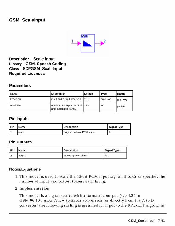
GSM_ScaleInput
Description Scale InputLibrary GSM, Speech CodingClass SDFGSM_ScaleInputRequired Licenses
Parameters
Pin Inputs
Pin Outputs
Notes/Equations
1. This model is used to scale the 13-bit PCM input signal. BlockSize specifies thenumber of input and output tokens each firing.
2. Implementation
This model is a signal source with a formatted output (see 4.20 inGSM 06.10). After A-law to linear conversion (or directly from the A to Dconverter) the following scaling is assumed for input to the RPE-LTP algorithm:
Name Description Default Type Range
Precision input and output precision. 16.0 precision [1.0,∞)
BlockSize number of samples to readand output per frame.
160 int (0,∞)
Pin Name Description Signal Type
1 input original uniform PCM signal. fix
Pin Name Description Signal Type
2 output scaled speech signal fix
GSM_ScaleInput 7-41

Speech Codec Components
s.v.v.v.v.v.v.v.v.v.v.v.v.x.x.x (twos-complement format),
where s is a sign bit, v is a valid bit, and x is a don't care bit.
The original signal is called Sop[..]; the Sop[..] format must be held.Downscaling occurs after the original Sop signal has formatted.
References
[1]European Telecommunications Standard Institute (ETSI), Rec. ETSI/GSM06.10, Full Rate Speech Transcoding, version 4.0.2, Sept. 1994.
7-42 GSM_ScaleInput
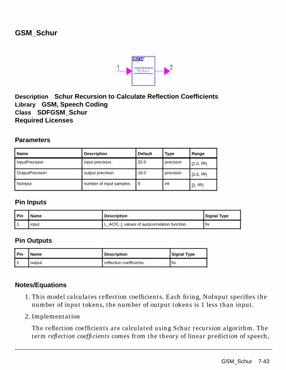
GSM_Schur
Description Schur Recursion to Calculate Reflection CoefficientsLibrary GSM, Speech CodingClass SDFGSM_SchurRequired Licenses
Parameters
Pin Inputs
Pin Outputs
Notes/Equations
1. This model calculates reflection coefficients. Each firing, NoInput specifies thenumber of input tokens, the number of output tokens is 1 less than input.
2. Implementation
The reflection coefficients are calculated using Schur recursion algorithm. Theterm reflection coefficients comes from the theory of linear prediction of speech,
Name Description Default Type Range
InputPrecision input precision. 32.0 precision [2.0,∞)
OutputPrecision output precision. 16.0 precision [2.0,∞)
NoInput number of input samples. 9 int [2,∞)
Pin Name Description Signal Type
1 input L_ACF[..], values of autocorrelation function. fix
Pin Name Description Signal Type
2 output reflection coefficients. fix
GSM_Schur 7-43
Speech Codec Components
where a vocal tract representation consisting of a series of uniform cylindricalsection is assumed. Such a representation can be described by the reflectioncoefficients or the area ratios of connected sections.
References
[1]European Telecommunications Standard Institute (ETSI), Rec. ETSI/GSM06.10, Full Rate Speech Transcoding, version 4.0.2, Sept. 1994.
7-44 GSM_Schur
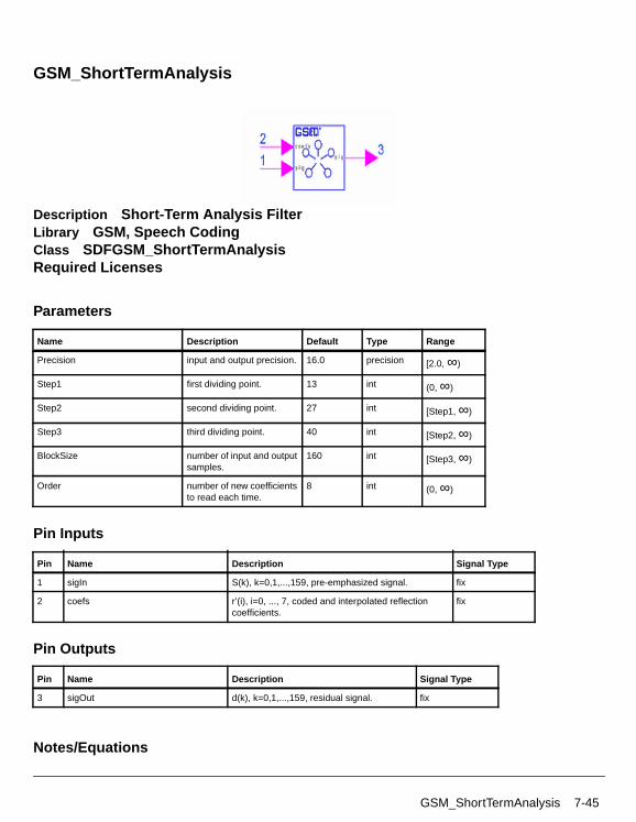
GSM_ShortTermAnalysis
Description Short-Term Analysis FilterLibrary GSM, Speech CodingClass SDFGSM_ShortTermAnalysisRequired Licenses
Parameters
Pin Inputs
Pin Outputs
Notes/Equations
Name Description Default Type Range
Precision input and output precision. 16.0 precision [2.0,∞)
Step1 first dividing point. 13 int (0,∞)
Step2 second dividing point. 27 int [Step1,∞)
Step3 third dividing point. 40 int [Step2,∞)
BlockSize number of input and outputsamples.
160 int [Step3,∞)
Order number of new coefficientsto read each time.
8 int (0,∞)
Pin Name Description Signal Type
1 sigIn S(k), k=0,1,...,159, pre-emphasized signal. fix
2 coefs r’(i), i=0, ..., 7, coded and interpolated reflectioncoefficients.
fix
Pin Name Description Signal Type
3 sigOut d(k), k=0,1,...,159, residual signal. fix
GSM_ShortTermAnalysis 7-45
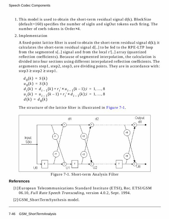
Speech Codec Components
1. This model is used to obtain the short-term residual signal d(k). BlockSize(default=160) specifies the number of sigIn and sigOut tokens each firing. Thenumber of coefs tokens is Order×4.
2. Implementation
A fixed-point lattice filter is used to obtain the short-term residual signal d(k); itcalculates the short-term residual signal d[..] to be fed to the RPE-LTP loopfrom the segmented s[..] signal and from the local r'[..] array (quantizedreflection coefficients). Because of segmented interpolation, the calculation isdivided into four sections using different interpolated reflection coefficients. Thearguments step1, step2, step3, are dividing points. They are in accordance with:step3 ≥ step2 ≥ step1.
The structure of the lattice filter is illustrated in Figure 7-1.
Figure 7-1. Short-term Analysis Filter
References
[1]European Telecommunications Standard Institute (ETSI), Rec. ETSI/GSM06.10, Full Rate Speech Transcoding, version 4.0.2, Sept. 1994.
[2] GSM_ShortTermSynthesis model.
d0 k( ) S k( )u0 k( ) S k( )di k( ) di 1– k( ) ri' ui 1– k 1–( )× i;+ 1 … 8ui k( )
, ,ui 1– k 1–( ) ri' di 1– k( )× i;+ 1 … 8
d k( ), ,
d8 k( )
=== == =
=
7-46 GSM_ShortTermAnalysis

GSM_ShortTermPredict
Description Estimate Short-Term Residual Signal.Library GSM, Speech CodingClass SDFGSM_ShortTermPredictRequired Licenses
Parameters
Pin Inputs
Pin Outputs
Notes/Equations
1. This model is used to decode LTP lags Ncj, gains bcj and estimate the short-termresidual signal d"(k). This is an inverse transformation ofGSM_LTP_Parameter.
Name Description Default Type Range
Precision input and output precision. 16.0 precision [2.0,∞)
BlockSize number of input and outputper sub-frame.
40 int [1,∞)
Pin Name Description Signal Type
1 LTPgn gain factor. fix
2 LTPlag LTP lag. fix
3 recons d’, reconstructed short-term residual signal. fix
Pin Name Description Signal Type
4 est d’’, estimate of the short-term residual signal. fix
GSM_ShortTermPredict 7-47

Speech Codec Components
Each firing, BlockSize (default=40) specifies the number of recons and esttokens. The number of tokens for LTPgn and LTPlag are fixed to 1.
2. Implementation
The bc parameter is decoded to determine the samples of the estimatedpp[0..39]. The long-term residual signal e[0..39] is calculated to be fed to thelong-term analysis filter.
Calculation of LTP parameters is implemented as follows:
• decode LTP Lags
• decode LTP gains
• estimate the short-term residual signal d''(k)
References
[1]European Telecommunications Standard Institute (ETSI), Rec. ETSI/GSM06.10, Full Rate Speech Transcoding, version 4.0.2, Sept. 1994.
b j' QLB bcj( ) j; 0 … 3, ,= =
d'' k j k+( ) b j' d' k j k N j'–+( )×
j 0 … 3, ,=
k 0 … , 39,=
k j k0 j 40×+=
;=
7-48 GSM_ShortTermPredict
GSM_ShortTermSynthesis
Description Inverse Transformation of Short-Term Analysis Filter.Library GSM, Speech CodingClass SDFGSM_ShortTermSynthesisRequired Licenses
Parameters
Pin Inputs
Pin Outputs
Notes/Equations
Name Description Default Type Range
Precision input and output precision. 16.0 precision [2.0,∞)
BlockSize number of input and outputsamples.
160 int [Step3,∞)
Order number of new coefficientsto read each time.
8 int (0,∞)
Step1 first dividing point. 13 int (0,∞)
Step2 second dividing point. 27 int [Step1,∞)
Step3 third dividing point. 40 int [Step2,∞)
Pin Name Description Signal Type
1 sigIn dr’(k), k=0,1,...,159, short-term residual signal. fix
2 coefs decoded reflection coefficients. fix
Pin Name Description Signal Type
3 sigOut Sr(k), k=0,1,...,159, output of short-term synthesisfilter.
fix
GSM_ShortTermSynthesis 7-49
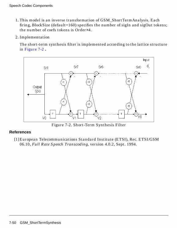
Speech Codec Components
1. This model is an inverse transformation of GSM_ShortTermAnalysis. Eachfiring, BlockSize (default=160) specifies the number of sigIn and sigOut tokens;the number of coefs tokens is Order×4.
2. Implementation
The short-term synthesis filter is implemented according to the lattice structurein Figure 7-2 .
Figure 7-2. Short-Term Synthesis Filter
References
[1]European Telecommunications Standard Institute (ETSI), Rec. ETSI/GSM06.10, Full Rate Speech Transcoding, version 4.0.2, Sept. 1994.
7-50 GSM_ShortTermSynthesis
GSM_SpeechDecoder
Description GSM Speech DecoderLibrary GSM, Speech CodingRequired Licenses
Parameters
Pin Inputs
Pin Outputs
Notes/Equations
1. This subnetwork is applicable for the full-rate traffic channel (TCH) in thePan-European Digital Mobile Radio (DMR) system.
2. Implementation
This subnetwork takes encoded blocks of 260 bits as input. The output isreconstructed 160 speech samples in 13-bit uniform PCM format. The output
Name Description Default Type Range
FrameSize speech frame length 160 int [1,∞)
SubFrameSize speech sub-frame length 40 int [1,∞)
RPE_Ratio upsample or downsampleratio for RPE
3 int [1,∞)
Pin Name Description Signal Type
1 input frame data packet(260 bits per 20 msec) int
Pin Name Description Signal Type
2 output reconstructed speech signal fix
GSM_SpeechDecoder 7-51
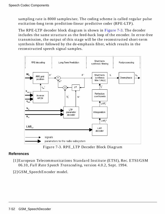
Speech Codec Components
sampling rate is 8000 samples/sec. The coding scheme is called regular pulseexcitation-long term prediction-linear predictive coder (RPE-LTP).
The RPE-LTP decoder block diagram is shown in Figure 7-3. The decoderincludes the same structure as the feed-back loop of the encoder. In error-freetransmission, the output of this stage will be the reconstructed short-termsynthesis filter followed by the de-emphasis filter, which results in thereconstructed speech signal samples.
Figure 7-3. RPE_LTP Decoder Block Diagram
References
[1]European Telecommunications Standard Institute (ETSI), Rec. ETSI/GSM06.10, Full Rate Speech Transcoding, version 4.0.2, Sept. 1994.
[2] GSM_SpeechEncoder model.
7-52 GSM_SpeechDecoder
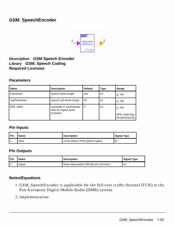
GSM_SpeechEncoder
Description GSM Speech EncoderLibrary GSM, Speech CodingRequired Licenses
Parameters
Pin Inputs
Pin Outputs
Notes/Equations
1. GSM_SpeechEncoder is applicable for the full-rate traffic channel (TCH) in thePan-European Digital Mobile Radio (DMR) system.
2. Implementation
Name Description Default Type Range
FrameSize speech frame length 160 int [1,∞)
SubFrameSize speech sub-frame length 40 int [1,∞)
RPE_Ratio upsample or downsampleratio for regular pulseexcitation
3 int [1,∞)
RPE_Ratio=[SubFrameSize/13]
Pin Name Description Signal Type
1 input 13-bit uniform PCM speech signal fix
Pin Name Description Signal Type
2 output frame data packet (260 bits per 20 msec) int
GSM_SpeechEncoder 7-53
Speech Codec Components
This subnetwork takes 160 speech samples in 13-bit uniform PCM format asinput. The output is encoded blocks of 260 bits. The sampling rate is 8000samples/sec leading to an average bit rate for the encoded bit stream of 13kbit/sec. The coding scheme is called regular pulse excitation-long termprediction-linear predictive coder (RPE-LTP).
The RPE-LTP encoder block diagram is shown in Figure 7-4. The input speechframe, consisting of 160 signal samples (uniform 13-bit PCM samples), ispre-processed to produce an offset-free signal that is then subjected to afirst-order pre-emphasis filter. The 160 samples obtained are analyzed todetermine the coefficients for the short-term analysis filter (LPC filter). Theseparameters are then used for the filtering of the same 160 samples. The resultis 160 samples of the short-term residual signal. The filter parameters, termedreflection coefficients, are transformed to Log.area ratios (LARs) beforetransmission.
For the following operations, the speech frame is divided into 4 sub-frames with40 samples of short-term residual signal in each. Each sub-frame is processedblockwise by the subsequent functional elements.
Before processing each sub-block of 40 short-term residual samples, theparameters of the long-term analysis filter, LTP lag, and LTP gain areestimated and updated in the LTP analysis block; this is done based on thecurrent sub-block of the present and a stored sequence of the 120 previousreconstructed short-term residual samples.
A block of 40 long-term residual signal samples is obtained by subtracting 40estimates of the short-term residual signal from the short-term residual signalitself. The resulting block of 40 long-term residual samples is fed to the RPEanalysis, which performs the basic compression function of the algorithm.
As a result of the RPE-analysis, the 40 long-term residual samples input blockis represented by one of 4 candidate sub-sequences of 13 pulses each. Thesub-sequence selected is identified by the RPE grid position (M). The 13 RPEpulse are encoded using adaptive pulse code modulation (APCM) withestimation of the sub-block amplitude, which is transmitted to the decoder asside information.
The RPE parameters are also fed to a local RPE decoding and reconstructionmodel, which produces a block of 40 samples of the quantized version of thelong-term residual signal.
7-54 GSM_SpeechEncoder
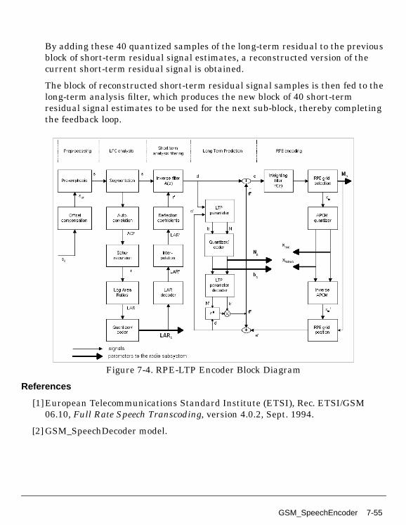
By adding these 40 quantized samples of the long-term residual to the previousblock of short-term residual signal estimates, a reconstructed version of thecurrent short-term residual signal is obtained.
The block of reconstructed short-term residual signal samples is then fed to thelong-term analysis filter, which produces the new block of 40 short-termresidual signal estimates to be used for the next sub-block, thereby completingthe feedback loop.
Figure 7-4. RPE-LTP Encoder Block Diagram
References
[1]European Telecommunications Standard Institute (ETSI), Rec. ETSI/GSM06.10, Full Rate Speech Transcoding, version 4.0.2, Sept. 1994.
[2] GSM_SpeechDecoder model.
GSM_SpeechEncoder 7-55
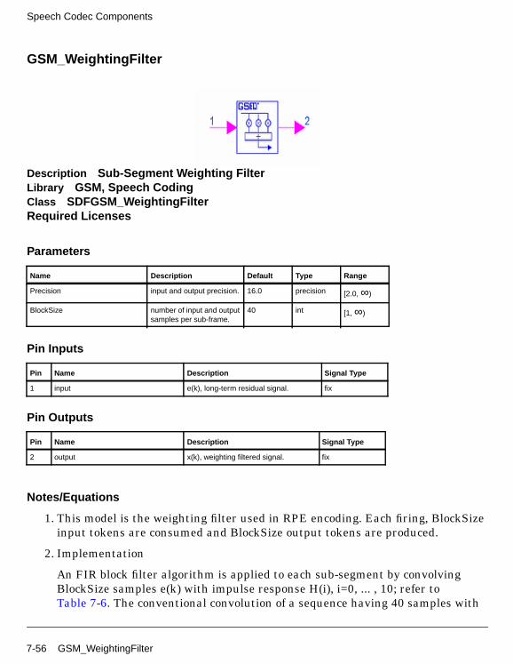
Speech Codec Components
GSM_WeightingFilter
Description Sub-Segment Weighting FilterLibrary GSM, Speech CodingClass SDFGSM_WeightingFilterRequired Licenses
Parameters
Pin Inputs
Pin Outputs
Notes/Equations
1. This model is the weighting filter used in RPE encoding. Each firing, BlockSizeinput tokens are consumed and BlockSize output tokens are produced.
2. Implementation
An FIR block filter algorithm is applied to each sub-segment by convolvingBlockSize samples e(k) with impulse response H(i), i=0, ... , 10; refer toTable 7-6. The conventional convolution of a sequence having 40 samples with
Name Description Default Type Range
Precision input and output precision. 16.0 precision [2.0,∞)
BlockSize number of input and outputsamples per sub-frame.
40 int [1,∞)
Pin Name Description Signal Type
1 input e(k), long-term residual signal. fix
Pin Name Description Signal Type
2 output x(k), weighting filtered signal. fix
7-56 GSM_WeightingFilter

an 11-tap impulse response would produce BlockSize+11−1 samples. Incontrast, the block filter algorithm produces the BlockSize central samples ofthe conventional convolution operation. For notation convenience theblock-filtered version of each sub-segment is denoted by x(k), k=0, ... , BlockSize− 1 (BlockSize default=40).
References
[1]European Telecommunications Standard Institute (ETSI), Rec. ETSI/GSM06.10, Full Rate Speech Transcoding, version 4.0.2, Sept. 1994.
Table 7-6. Impulse Response of Block (Weighting) Filteri 5 4(6) 3(7) 2(8) 1(9) 0(10)
H(i)×213 8192 5741 2054 0 −374 −134
x k( ) H i( ) e k 5 i–+( ) k;×i 0=
10
∑ 0 … 39
e k 5 i–+( )
, ,
0 for k+5-i 0 and k+5-i 39><;
= =
=
GSM_WeightingFilter 7-57

Speech Codec Components
GSM_WriteFile
Description Write Data to a Binary FileLibrary GSM, Speech CodingClass SDFGSM_WriteFileRequired Licenses
Parameters
Pin Inputs
Notes/Equations
1. This model is used to demonstrate and test speech codec. It receives shortinteger data and saves it in a binary file. Each firing, one input token isconsumed.
2. For FileType: select dos_type for PC platforms; select unix_type for (HP andSun) UNIX platforms.
Name Description Default Type
FileName output wav file name. output.wav filename
FileType file type: dos_type,unix_type
dos_type enum
Pin Name Description Signal Type
1 input decoder output int
7-58 GSM_WriteFile

Chapter 8: Synchronization Components
8-1
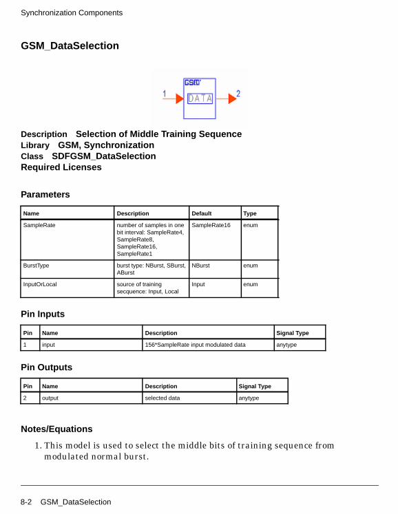
Synchronization Components
GSM_DataSelection
Description Selection of Middle Training SequenceLibrary GSM, SynchronizationClass SDFGSM_DataSelectionRequired Licenses
Parameters
Pin Inputs
Pin Outputs
Notes/Equations
1. This model is used to select the middle bits of training sequence frommodulated normal burst.
Name Description Default Type
SampleRate number of samples in onebit interval: SampleRate4,SampleRate8,SampleRate16,SampleRate1
SampleRate16 enum
BurstType burst type: NBurst, SBurst,ABurst
NBurst enum
InputOrLocal source of trainingsecquence: Input, Local
Input enum
Pin Name Description Signal Type
1 input 156*SampleRate input modulated data anytype
Pin Name Description Signal Type
2 output selected data anytype
8-2 GSM_DataSelection
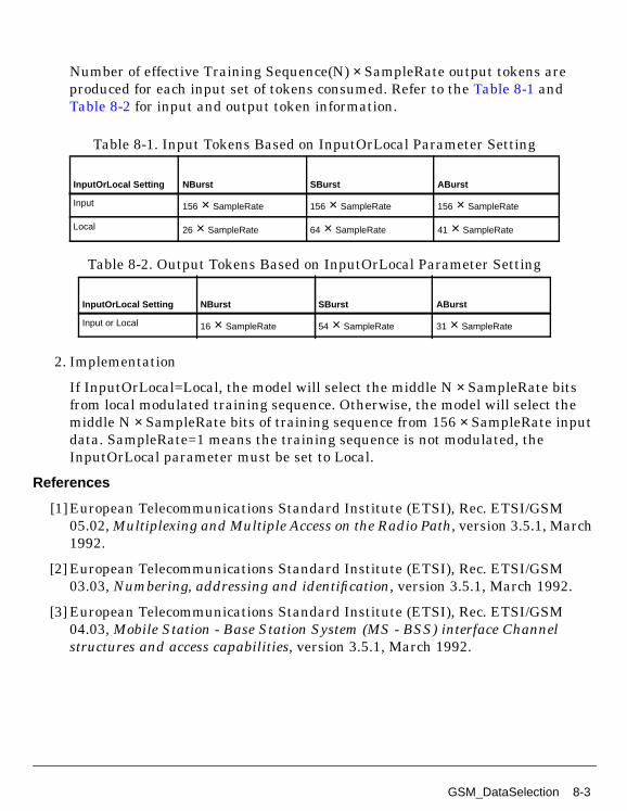
Number of effective Training Sequence(N) × SampleRate output tokens areproduced for each input set of tokens consumed. Refer to the Table 8-1 andTable 8-2 for input and output token information.
2. Implementation
If InputOrLocal=Local, the model will select the middle N × SampleRate bitsfrom local modulated training sequence. Otherwise, the model will select themiddle N × SampleRate bits of training sequence from 156 × SampleRate inputdata. SampleRate=1 means the training sequence is not modulated, theInputOrLocal parameter must be set to Local.
References
[1]European Telecommunications Standard Institute (ETSI), Rec. ETSI/GSM05.02, Multiplexing and Multiple Access on the Radio Path, version 3.5.1, March1992.
[2] European Telecommunications Standard Institute (ETSI), Rec. ETSI/GSM03.03, Numbering, addressing and identification, version 3.5.1, March 1992.
[3] European Telecommunications Standard Institute (ETSI), Rec. ETSI/GSM04.03, Mobile Station - Base Station System (MS - BSS) interface Channelstructures and access capabilities, version 3.5.1, March 1992.
Table 8-1. Input Tokens Based on InputOrLocal Parameter Setting
InputOrLocal Setting NBurst SBurst ABurst
Input 156 × SampleRate 156 × SampleRate 156 × SampleRate
Local 26 × SampleRate 64 × SampleRate 41 × SampleRate
Table 8-2. Output Tokens Based on InputOrLocal Parameter Setting
InputOrLocal Setting NBurst SBurst ABurst
Input or Local 16 × SampleRate 54 × SampleRate 31 × SampleRate
GSM_DataSelection 8-3
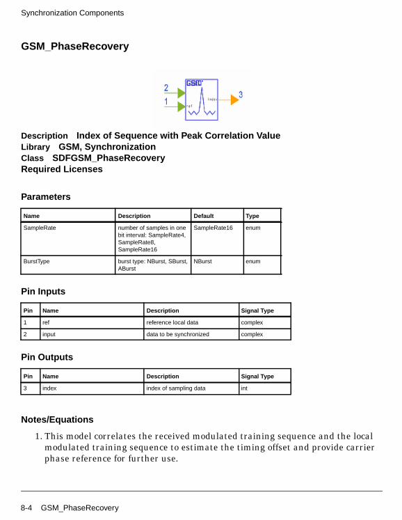
Synchronization Components
GSM_PhaseRecovery
Description Index of Sequence with Peak Correlation ValueLibrary GSM, SynchronizationClass SDFGSM_PhaseRecoveryRequired Licenses
Parameters
Pin Inputs
Pin Outputs
Notes/Equations
1. This model correlates the received modulated training sequence and the localmodulated training sequence to estimate the timing offset and provide carrierphase reference for further use.
Name Description Default Type
SampleRate number of samples in onebit interval: SampleRate4,SampleRate8,SampleRate16
SampleRate16 enum
BurstType burst type: NBurst, SBurst,ABurst
NBurst enum
Pin Name Description Signal Type
1 ref reference local data complex
2 input data to be synchronized complex
Pin Name Description Signal Type
3 index index of sampling data int
8-4 GSM_PhaseRecovery
Each firing, one token is produced per input set of tokens; 16 × SampleRate reftokens are consumed; 16 × SampleRate input tokens are consumed.
References
[1]G. D’Aria, F. Muratore, Simulation and Performance of the Pan-European LandMobile Radio System, IEEE Trans. on Vehicular Technology, Vol. 41, pp.177-189, No.2, May 1992.
GSM_PhaseRecovery 8-5

Synchronization Components
GSM_PhsRcvryTrNoMod
Description Index of Sequence with Peak Correlation Value (Training Bits NotModulated)Library GSM, SynchronizationClass SDFGSM_PhsRcvryTrNoModRequired Licenses
Parameters
Pin Inputs
Pin Outputs
Notes/Equations
1. This model is used to correlate the received modulated training sequence andthe local training sequence, which is not modulated, to estimate the timingoffset and provide the carrier phase reference for use later.
Name Description Default Type
SampleRate number of samples in onebit interval: SampleRate4,SampleRate8,SampleRate16
SampleRate16 enum
Pin Name Description Signal Type
1 ref reference local training sequence int
2 input data to be synchronized complex
Pin Name Description Signal Type
3 index index of sampling data int
8-6 GSM_PhsRcvryTrNoMod
One token is produced for each set of input tokens;ref = SampleRate input tokens are consumed each firing;input = 16 × SampleRate input tokens are consumed each firing.
References
[1]G. D’Aria, F. Muratore, Simulation and Performance of the Pan- European LandMobile Radio System, IEEE Trans. on Vehicular Technology, Vol. 41, May 1992,pp. 177-189.
GSM_PhsRcvryTrNoMod 8-7
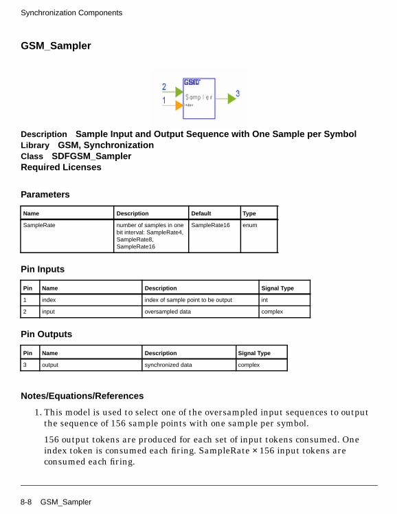
Synchronization Components
GSM_Sampler
Description Sample Input and Output Sequence with One Sample per SymbolLibrary GSM, SynchronizationClass SDFGSM_SamplerRequired Licenses
Parameters
Pin Inputs
Pin Outputs
Notes/Equations/References
1. This model is used to select one of the oversampled input sequences to outputthe sequence of 156 sample points with one sample per symbol.
156 output tokens are produced for each set of input tokens consumed. Oneindex token is consumed each firing. SampleRate × 156 input tokens areconsumed each firing.
Name Description Default Type
SampleRate number of samples in onebit interval: SampleRate4,SampleRate8,SampleRate16
SampleRate16 enum
Pin Name Description Signal Type
1 index index of sample point to be output int
2 input oversampled data complex
Pin Name Description Signal Type
3 output synchronized data complex
8-8 GSM_Sampler

2. Implementation
After SampleRate × 156 sample points are received, the model divides them intoSampleRate sequences; all first sample points of each symbol construct the firstsequence, all second sample points of each symbol construct the secondsequence, and so on. After the model receives input index, it selects one of thesequences and output.
References
[2] G. D’Aria, F. Muratore, Simulation and Performance of the Pan- European LandMobile Radio System, IEEE Trans. on Vehicular Technology, Vol. 41, May 1992,pp. 177-189.
GSM_Sampler 8-9
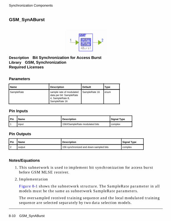
Synchronization Components
GSM_SynABurst
Description Bit Synchronization for Access BurstLibrary GSM, SynchronizationRequired Licenses
Parameters
Pin Inputs
Pin Outputs
Notes/Equations
1. This subnetwork is used to implement bit synchronization for access burstbefore GSM MLSE receiver.
2. Implementation
Figure 8-1 shows the subnetwork structure. The SampleRate parameter in allmodels must be the same as subnetwork SampleRate parameters.
The oversampled received training sequence and the local modulated trainingsequence are selected separately by two data selection models.
Name Description Default Type
SampleRate sample rate of modulateddata per bit: SampleRate4, SampleRate 8,SampleRate 16
SampleRate 16 enum
Pin Name Description Signal Type
1 input 156XSampleRate modulated bits complex
Pin Name Description Signal Type
2 output 156 synchronized and down-sampled bits complex
8-10 GSM_SynABurst
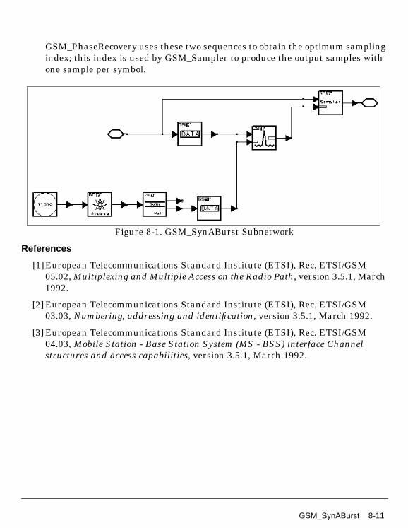
GSM_PhaseRecovery uses these two sequences to obtain the optimum samplingindex; this index is used by GSM_Sampler to produce the output samples withone sample per symbol.
Figure 8-1. GSM_SynABurst Subnetwork
References
[1]European Telecommunications Standard Institute (ETSI), Rec. ETSI/GSM05.02, Multiplexing and Multiple Access on the Radio Path, version 3.5.1, March1992.
[2] European Telecommunications Standard Institute (ETSI), Rec. ETSI/GSM03.03, Numbering, addressing and identification, version 3.5.1, March 1992.
[3] European Telecommunications Standard Institute (ETSI), Rec. ETSI/GSM04.03, Mobile Station - Base Station System (MS - BSS) interface Channelstructures and access capabilities, version 3.5.1, March 1992.
GSM_SynABurst 8-11
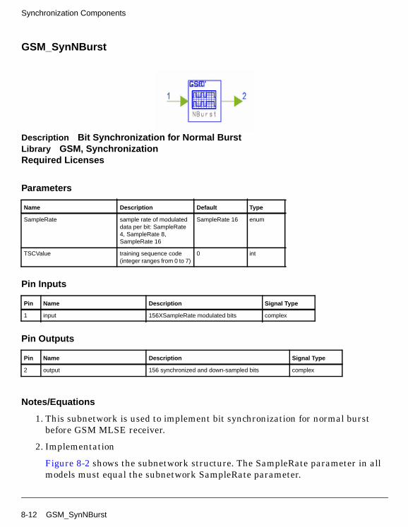
Synchronization Components
GSM_SynNBurst
Description Bit Synchronization for Normal BurstLibrary GSM, SynchronizationRequired Licenses
Parameters
Pin Inputs
Pin Outputs
Notes/Equations
1. This subnetwork is used to implement bit synchronization for normal burstbefore GSM MLSE receiver.
2. Implementation
Figure 8-2 shows the subnetwork structure. The SampleRate parameter in allmodels must equal the subnetwork SampleRate parameter.
Name Description Default Type
SampleRate sample rate of modulateddata per bit: SampleRate4, SampleRate 8,SampleRate 16
SampleRate 16 enum
TSCValue training sequence code(integer ranges from 0 to 7)
0 int
Pin Name Description Signal Type
1 input 156XSampleRate modulated bits complex
Pin Name Description Signal Type
2 output 156 synchronized and down-sampled bits complex
8-12 GSM_SynNBurst
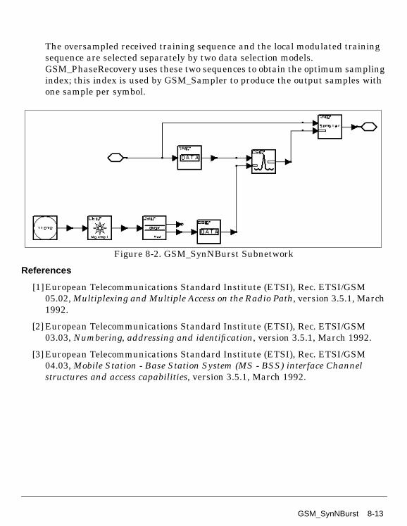
The oversampled received training sequence and the local modulated trainingsequence are selected separately by two data selection models.GSM_PhaseRecovery uses these two sequences to obtain the optimum samplingindex; this index is used by GSM_Sampler to produce the output samples withone sample per symbol.
Figure 8-2. GSM_SynNBurst Subnetwork
References
[1]European Telecommunications Standard Institute (ETSI), Rec. ETSI/GSM05.02, Multiplexing and Multiple Access on the Radio Path, version 3.5.1, March1992.
[2] European Telecommunications Standard Institute (ETSI), Rec. ETSI/GSM03.03, Numbering, addressing and identification, version 3.5.1, March 1992.
[3] European Telecommunications Standard Institute (ETSI), Rec. ETSI/GSM04.03, Mobile Station - Base Station System (MS - BSS) interface Channelstructures and access capabilities, version 3.5.1, March 1992.
GSM_SynNBurst 8-13
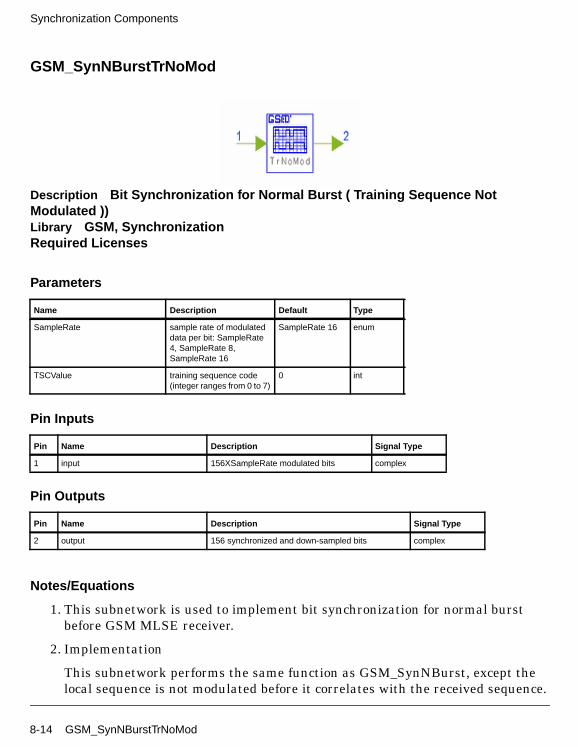
Synchronization Components
GSM_SynNBurstTrNoMod
Description Bit Synchronization for Normal Burst ( Training Sequence NotModulated ))Library GSM, SynchronizationRequired Licenses
Parameters
Pin Inputs
Pin Outputs
Notes/Equations
1. This subnetwork is used to implement bit synchronization for normal burstbefore GSM MLSE receiver.
2. Implementation
This subnetwork performs the same function as GSM_SynNBurst, except thelocal sequence is not modulated before it correlates with the received sequence.
Name Description Default Type
SampleRate sample rate of modulateddata per bit: SampleRate4, SampleRate 8,SampleRate 16
SampleRate 16 enum
TSCValue training sequence code(integer ranges from 0 to 7)
0 int
Pin Name Description Signal Type
1 input 156XSampleRate modulated bits complex
Pin Name Description Signal Type
2 output 156 synchronized and down-sampled bits complex
8-14 GSM_SynNBurstTrNoMod
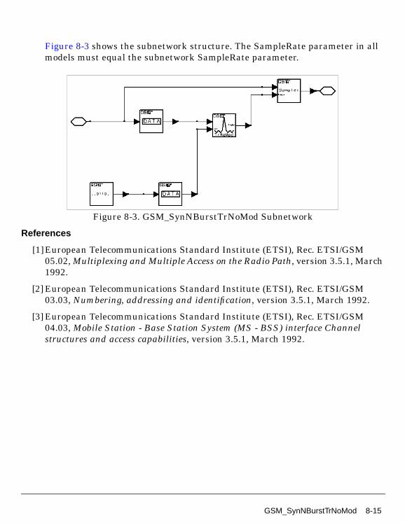
Figure 8-3 shows the subnetwork structure. The SampleRate parameter in allmodels must equal the subnetwork SampleRate parameter.
Figure 8-3. GSM_SynNBurstTrNoMod Subnetwork
References
[1]European Telecommunications Standard Institute (ETSI), Rec. ETSI/GSM05.02, Multiplexing and Multiple Access on the Radio Path, version 3.5.1, March1992.
[2] European Telecommunications Standard Institute (ETSI), Rec. ETSI/GSM03.03, Numbering, addressing and identification, version 3.5.1, March 1992.
[3] European Telecommunications Standard Institute (ETSI), Rec. ETSI/GSM04.03, Mobile Station - Base Station System (MS - BSS) interface Channelstructures and access capabilities, version 3.5.1, March 1992.
GSM_SynNBurstTrNoMod 8-15
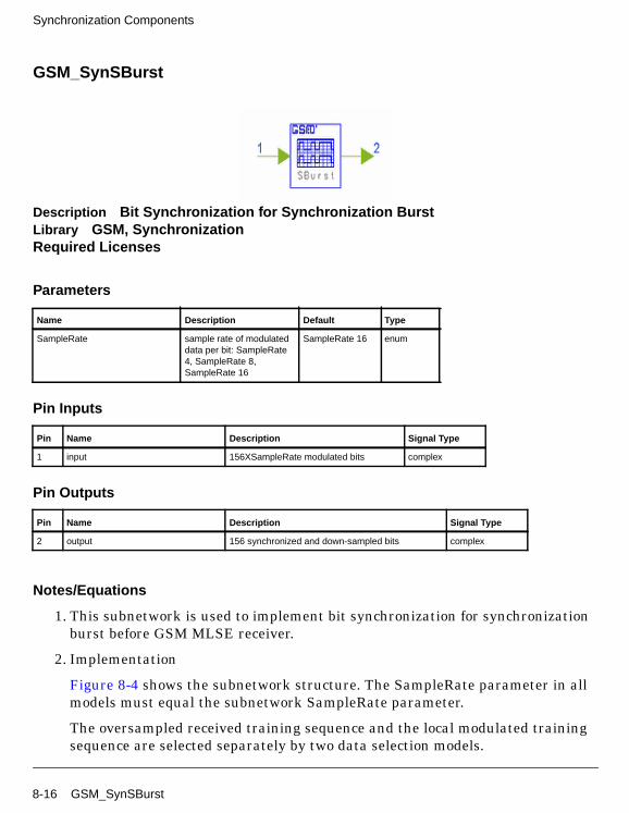
Synchronization Components
GSM_SynSBurst
Description Bit Synchronization for Synchronization BurstLibrary GSM, SynchronizationRequired Licenses
Parameters
Pin Inputs
Pin Outputs
Notes/Equations
1. This subnetwork is used to implement bit synchronization for synchronizationburst before GSM MLSE receiver.
2. Implementation
Figure 8-4 shows the subnetwork structure. The SampleRate parameter in allmodels must equal the subnetwork SampleRate parameter.
The oversampled received training sequence and the local modulated trainingsequence are selected separately by two data selection models.
Name Description Default Type
SampleRate sample rate of modulateddata per bit: SampleRate4, SampleRate 8,SampleRate 16
SampleRate 16 enum
Pin Name Description Signal Type
1 input 156XSampleRate modulated bits complex
Pin Name Description Signal Type
2 output 156 synchronized and down-sampled bits complex
8-16 GSM_SynSBurst
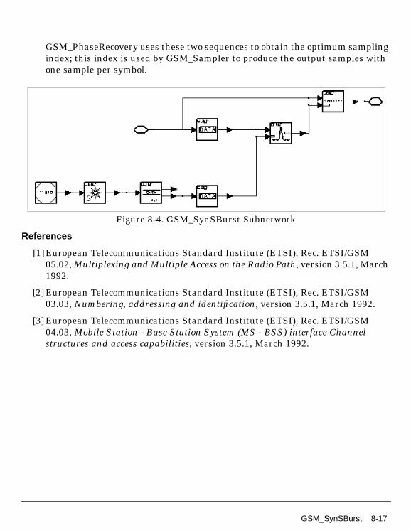
GSM_PhaseRecovery uses these two sequences to obtain the optimum samplingindex; this index is used by GSM_Sampler to produce the output samples withone sample per symbol.
Figure 8-4. GSM_SynSBurst Subnetwork
References
[1]European Telecommunications Standard Institute (ETSI), Rec. ETSI/GSM05.02, Multiplexing and Multiple Access on the Radio Path, version 3.5.1, March1992.
[2] European Telecommunications Standard Institute (ETSI), Rec. ETSI/GSM03.03, Numbering, addressing and identification, version 3.5.1, March 1992.
[3] European Telecommunications Standard Institute (ETSI), Rec. ETSI/GSM04.03, Mobile Station - Base Station System (MS - BSS) interface Channelstructures and access capabilities, version 3.5.1, March 1992.
GSM_SynSBurst 8-17

Synchronization Components
GSM_TrainBitGen
Description Training Bits GenerationLibrary GSM, SynchronizationClass SDFGSM_TrainBitGenRequired Licenses
Parameters
Pin Outputs
Notes/Equations
1. This model is used to generate training sequences.
BurstType=NBurst, 26 tokens are producedBurstType=ABurst, 41 output tokens are producedBurstType=SBurst, 64 output tokens are produced
2. Implementation
Table 8-3 shows the training sequence output according to TSC. TSC is ignoredwhen BurstType=ABurst or SBurst.
The synchronization burst synchronization sequence is:
{1,0,1,1,1,0,0,1,0,1,1,0,0,0,1,0,0,0,0,0,0,1,0,0,0,0,0,0,1,1,1,1,0,0,1,0,1,1,0,1,0,1,0,0,0,1,0,1,0,1, 1,1,0,1,1,0,0,0,0,1,1,0,1,1}
Name Description Default Type Range
BurstType burst type: NBurst, SBurst,ABurst
NBurst enum
TSC training secquence code 0 int [0, 7]
Pin Name Description Signal Type
1 output training sequence int
8-18 GSM_TrainBitGen

The access burst synchronization sequence is:
{0,1,0,0,1,0,1,1,0,1,1,1,1,1,1,1,1,0,0,1,1,0,0,1,1,0,1,0,1,0,1,0,0,0,1,1,1,1,0,0,0}
References
[1]European Telecommunications Standard Institute (ETSI), Rec. ETSI/GSM05.02, Multiplexing and Multiple Access on the Radio Path, version 3.5.1, March1992.
[2] European Telecommunications Standard Institute (ETSI), Rec. ETSI/GSM03.03, Numbering, addressing and identification, version 3.5.1, March 1992.
[3] European Telecommunications Standard Institute (ETSI), Rec. ETSI/GSM04.03, Mobile Station - Base Station System (MS - BSS) interface Channelstructures and access capabilities, version 3.5.1, March 1992.
Table 8-3. TSC and Training Sequences
TSC= Training Sequence
0 0,0,1,0,0,1,0,1,1,1,0,0,0,0,1,0,0,0,1,0,0,1,0,1,1,1
1 0,0,1,0,1,1,0,1,1,1,0,1,1,1,1,0,0,0,1,0,1,1,0,1,1,1
2 0,1,0,0,0,0,1,1,1,0,1,1,1,0,1,0,0,1,0,0,0,0,1,1,1,0
3 0,1,0,0,0,1,1,1,1,0,1,1,0,1,0,0,0,1,0,0,0,1,1,1,1,0
4 0,0,0,1,1,0,1,0,1,1,1,0,0,1,0,0,0,0,0,1,1,0,1,0,1,1
5 0,1,0,0,1,1,1,0,1,0,1,1,0,0,0,0,0,1,0,0,1,1,1,0,1,0
6 1,0,1,0,0,1,1,1,1,1,0,1,1,0,0,0,1,0,1,0,0,1,1,1,1,1
7 1,1,1,0,1,1,1,1,0,0,0,1,0,0,1,0,1,1,1,0,1,1,1,1,0,0
GSM_TrainBitGen 8-19
Synchronization Components
8-20
Chapter 9: GSM Design ExamplesThese design examples are provided in the /examples/gsm directory.
9-1
GSM Design Examples
Error Distribution Analysis of Adaptive Equalizer inNormal BurstEquErrPattern_prj Design Name
• GSM_BurstErrorPattern.dsn
Features
• Displays error distribution in GSM normal burst
• Fading channel with additive white Gaussian noise
• Adaptive equalizer uses maximum-likelihood sequence estimation
• Tcl/Tk plot for interactive display
Description
This example demonstrates an error pattern analysis throughout a normal burst toshow the adaptive equalizer performance. In transmission, a random bit sourcecomponent is used as channel coded data source. The data and training sequence areused in constructing a normal burst. After GMSK modulation, the signal istransmitted though a fading GSM channel, and additive Gaussian noise is added tothe received signal. A downsample component is used instead of a normal burst bitsynchronization component. The adaptive equalizer implements demodulation of thesignal output from the receiver (Butterworth) filter. The bit error rate of each positionin normal burst is statistically calculated by an error pattern display component andoutput to an interactive plot component for display.
In the adaptive equalizer, maximum-likelihood sequence estimation is used toimplement demodulation. The bits in the middle of normal burst have the lowestBER because the training sequence in the middle of normal burst is used to estimatethe channel characteristic using maximum-likelihood sequence estimation. The BERis increased from the center of normal burst to the both ends, which means that theperformance of equalizer is greatly affected by channel estimation accuracy.
9-2 Error Distribution Analysis of Adaptive Equalizer in Normal Burst
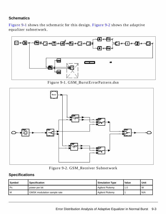
Schematics
Figure 9-1 shows the schematic for this design. Figure 9-2 shows the adaptiveequalizer subnetwork.
Figure 9-1. GSM_BurstErrorPattern.dsn
Figure 9-2. GSM_Receiver Subnetwork
Specifications
Symbol Specification Simulation Type Value Unit
Pc power per bit Agilent Ptolemy 1.0 W
M GMSK modulation sample rate Agilent Ptolemy 1 N/A
Error Distribution Analysis of Adaptive Equalizer in Normal Burst 9-3

GSM Design Examples
Notes
• Sample Rate is 4, 8, or 16 when M is 0, 1 or 2, respectively.
• TStep must be related to M, that is SampleRate=8 andTStep=3.69/SampleRate µsec.
Simulation Results
The results, shown in Figure 9-3, are obtained with a TU50 channel, no frequencyoffset, and SNR is 7.6 dB.
Figure 9-3. Error Pattern throughout Normal Burst
Benchmark
• Hardware Platform: Pentium Pro 200 MHz, 96 MB memory
• Software Platform: Windows NT 4.0 Workstation, Advanced Design System 1.1
• Data Points: 100000 frames
• Simulation Time: approximately 16 hours
TSC training sequence code Agilent Ptolemy 0 N/A
TStep output time step for channel model Agilent Ptolemy 3.692/8 µsec
Symbol Specification Simulation Type Value Unit
9-4 Error Distribution Analysis of Adaptive Equalizer in Normal Burst
Fast Associated Control ChannelFACCHsys_prj Design Name
• GSM_SysFACCH.dsn
Features
• GSM propagation fading channel and additive white Gaussian noise
• Fast associated control channel
• Channel interleaving and de-interleaving
• GMSK modulator and maximum-likelihood sequence estimation equalizer
• Gaussian noise with adjustable noise variance
• BER and FER performance stored in NumericSink
Description
This example shows the system performance of BER and FER on fast associatedcontrol channel. It consists of error correction encoding and decoding, interleavingand de-interleaving, data framing and deframing, GMSK modulation, GSM fadingchannel plus AWGN, 7-order Butterworth filter, bit synchronization andmaximum-likelihood sequence estimation receiver.
In fast associated control channel, a Fire code with tail bits, a convolutional code andblock diagonal interleaver are used. Each 184 data bits are transformed into 456 bitsafter channel coding and interleaving.
For details about framing, GMSK modulation, synchronization and MLSE reception,refer to Traffic Channel for Data Transmission at 9.6 kbps.
Schematics
Figure 9-4 shows the schematic for this design. Data source is a random bit sequence(B1).
Figure 9-5 shows the GSM_FACCH_Encoder subnetwork used in Figure 9-4 (detailedimplementation of channel coding and interleaving for fast associated controlchannel). The number of input and output bits of cyclic encoder are 184 and 224,respectively. 4 tail bits are added to the cyclic coded data. These 228 bits areconvolutionally encoded to 456 bits with constraint length of 5 and rate of 1/2.GSM_Interleaver_8 is used to interleave the input 456 bits into eight blocks.
Figure 9-6 shows GSM_FACCH_Decoder subnetwork.
Fast Associated Control Channel 9-5

GSM Design Examples
Figure 9-4. GSM_SysFACCH.dsn
Figure 9-5. GSM_FACCH_Encoder Subnetwork
Figure 9-6. GSM_FACCH_Decoder Subnetwork
Specifications
Symbol Specification Simulation Type Value Unit
GlobalPc power per bit Agilent Ptolemy 1e-3 W
FCarrier carrier frequency Agilent Ptolemy 900 MHz
SR sample rate Agilent Ptolemy 8 N/A
TStep output time step for channel model Agilent Ptolemy 3.692/8 µsec
9-6 Fast Associated Control Channel
Notes
• TStep must be related to SR, that is TStep=3.69/SR µsec.
• The input of the system is delayed by 184 bits before the BER, FERmeasurement.
Simulation Results
Figure 9-7 shows bit error and BER and frame error and FER.
Test Conditions
• Channel Type: TU50 (urban area, 50 km/hr)
• SNR: 16.9 dB
• FER test results: 0.48%
• Recommended (GSM Specification 05.05) FER: 8%
Benchmark
• Hardware Platform: Pentium Pro 200 MHz, 96 MB memory
• Software Platform: Windows NT 4.0 Workstation, Advanced Design System 1.1
• Data Points: 10000 frames
• Simulation Time: approximately 16 hours
Fast Associated Control Channel 9-7

GSM Design Examples
Figure 9-7. BER and FER
9-8 Fast Associated Control Channel
GMSK Modulation SpectrumGMSKModSpec_prj Design Name
• GSM_GMSKModSpectrum.dsn
Features
• GMSK modulation complying with GSM specification
• Adjustable sample rate
• Displays spectrum analysis
• Integrated RF section
Description
This example shows GMSK modulation (BTb=0.3, B is 3 db bandwidth for Gaussianfilter, Tb is bit time) and performs spectrum analysis. The GMSK modulation model isused to generate GMSK modulated signal, which is represented by complex envelopeequivalent and carrier frequency; it also performs differential encoding.
GMSK modulation is recommended for GSM systems with BTb=0.3 and rate 270.833kbits/s. GMSK is a type of constant-envelope FSK, where frequency modulation is aresult of carefully planned phase modulation. The frequency shifting in GMSK comesfrom carefully steering the phase of the carrier in quadrature so as to yield acontinuous phase transition. The most important feature of GMSK is that it is aconstant-envelope variety of modulation. This means there is a distinct lack of AM inthe carrier with a consequent limiting of the occupied bandwidth. The constantamplitude of the GMSK signal makes it suitable for use with high-efficiencyamplifiers.
The GSM_GMSKMod subnetwork receives the bit stream and produces modulatedsignal xg(t). Instead of generating xg(t) directly, we use complex envelope equivalentof xg(t) and carrier frequency fc to represent it. This sub-network is composed ofGSM_DifferEncoder, GSM_Rom and GSM_Carrier. After baseband modulation, thesignal is fed to the RF section, which consists of RF mixer, Butterworth filter, and RFgains.
Schematics
Figure 9-8 shows the schematic for this design. It contains Bit source,GSM_GMSKMod, CxToTimed, RF section, a spectrum analyzer, and a timed sink.The source of GMSK modulation can be any 0 or 1 signal. GMSK modulation
GMSK Modulation Spectrum 9-9
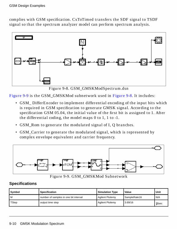
GSM Design Examples
complies with GSM specification. CxToTimed transfers the SDF signal to TSDFsignal so that the spectrum analyzer model can perform spectrum analysis.
Figure 9-8. GSM_GMSKModSpectrum.dsn
Figure 9-9 is the GSM_GMSKMod subnetwork used in Figure 9-8. It includes:
• GSM_ DifferEncoder to implement differential encoding of the input bits whichis required in GSM specification to generate GMSK signal. According to thespecification GSM 05.04, the initial value of the first bit is assigned to 1. Afterthe differential coding, the model maps 0 to 1, 1 to -1.
• GSM_Rom to generate the modulated signal of I, Q branches.
• GSM_Carrier to generate the modulated signal, which is represented bycomplex envelope equivalent and carrier frequency.
Figure 9-9. GSM_GMSKMod Subnetwork
Specifications
Symbol Specification Simulation Type Value Unit
M number of samples in one bit interval Agilent Ptolemy SampleRate16 N/A
TStep output time step Agilent Ptolemy 3.69/16 µsec
9-10 GMSK Modulation Spectrum
Notes
• TStep must be related to M, that is TStep=3.69/Samplerate µsec.
Simulation Results
Figure 9-10 shows the magnitude, phase and spectrum of the GMSK modulated data.The central frequency is 935.2 MHz. Figure 9-11 shows the spectrum of themodulated signal when inputs are all zero. We can see that the center frequency is67.7 kHz up shift from the center frequency 935.2 MHz, which is consistent with theGSM specification.
Benchmark
• Hardware platform: Pentium Pro 200 MHz, 96 MB memory
• Software platform: Windows NT 4.0 Workstation, Advanced Design System 1.1
• Data points: 6000 frames
• Simulation time: approximately 30 seconds
Window spectrum window type Agilent Ptolemy Flat_Top N/A
RF frequency RF central frequency Agilent Ptolemy 935.2 MHz
Symbol Specification Simulation Type Value Unit
GMSK Modulation Spectrum 9-11
GSM Design Examples
Figure 9-10. Magnitude, Phase and Spectrum for0.3 GMSK Modulated Random Signal
Figure 9-11. Spectrum of the 0.3GMSK Modulated All-Zero Signal
9-12 GMSK Modulation Spectrum
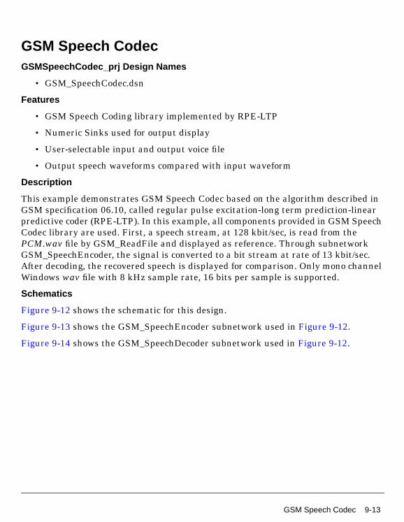
GSM Speech CodecGSMSpeechCodec_prj Design Names
• GSM_SpeechCodec.dsn
Features
• GSM Speech Coding library implemented by RPE-LTP
• Numeric Sinks used for output display
• User-selectable input and output voice file
• Output speech waveforms compared with input waveform
Description
This example demonstrates GSM Speech Codec based on the algorithm described inGSM specification 06.10, called regular pulse excitation-long term prediction-linearpredictive coder (RPE-LTP). In this example, all components provided in GSM SpeechCodec library are used. First, a speech stream, at 128 kbit/sec, is read from thePCM.wav file by GSM_ReadFile and displayed as reference. Through subnetworkGSM_SpeechEncoder, the signal is converted to a bit stream at rate of 13 kbit/sec.After decoding, the recovered speech is displayed for comparison. Only mono channelWindows wav file with 8 kHz sample rate, 16 bits per sample is supported.
Schematics
Figure 9-12 shows the schematic for this design.
Figure 9-13 shows the GSM_SpeechEncoder subnetwork used in Figure 9-12.
Figure 9-14 shows the GSM_SpeechDecoder subnetwork used in Figure 9-12.
GSM Speech Codec 9-13
GSM Design Examples
Figure 9-12. GSM_SpeechCodec.dsn
Figure 9-13. GSM_SpeechEncoder Subnetwork
9-14 GSM Speech Codec

Figure 9-14. GSM_SpeechDecoder Subnetwork
Specifications
Notes
• Parameters in GSM_SpeechDecoder such as FrameSize and SubFrameSizemust be consistent with GSM_SpeechEncoder.
• The default path for input and output file is the data directory under thecurrent project. The path and file name is user-settable.
Simulation Results
Figure 9-15 shows that the waveform of the recovered signal is close to the inputsignal.
Specification Simulation Type Value Unit
input sample rate Agilent Ptolemy 8 kHz
input bit rate Agilent Ptolemy 128 kbps
output sample rate Agilent Ptolemy 8 kHz
output bit rate Agilent Ptolemy 13 kbps
GSM Speech Codec 9-15
GSM Design Examples
Figure 9-15. Comparison of Input and Output Speech Waveforms
Benchmark
• Hardware platform: Pentium Pro 200 MHz, 96 MB memory
• Software platform: Windows NT 4.0 Workstation, Advanced Design System 1.1
• Data points: 10000 points
• Simulation time: approximately 2 minutes
9-16 GSM Speech Codec
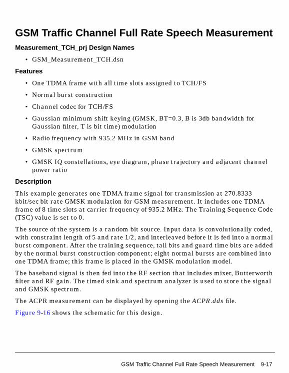
GSM Traffic Channel Full Rate Speech MeasurementMeasurement_TCH_prj Design Names
• GSM_Measurement_TCH.dsn
Features
• One TDMA frame with all time slots assigned to TCH/FS
• Normal burst construction
• Channel codec for TCH/FS
• Gaussian minimum shift keying (GMSK, BT=0.3, B is 3db bandwidth forGaussian filter, T is bit time) modulation
• Radio frequency with 935.2 MHz in GSM band
• GMSK spectrum
• GMSK IQ constellations, eye diagram, phase trajectory and adjacent channelpower ratio
Description
This example generates one TDMA frame signal for transmission at 270.8333kbit/sec bit rate GMSK modulation for GSM measurement. It includes one TDMAframe of 8 time slots at carrier frequency of 935.2 MHz. The Training Sequence Code(TSC) value is set to 0.
The source of the system is a random bit source. Input data is convolutionally coded,with constraint length of 5 and rate 1/2, and interleaved before it is fed into a normalburst component. After the training sequence, tail bits and guard time bits are addedby the normal burst construction component; eight normal bursts are combined intoone TDMA frame; this frame is placed in the GMSK modulation model.
The baseband signal is then fed into the RF section that includes mixer, Butterworthfilter and RF gain. The timed sink and spectrum analyzer is used to store the signaland GMSK spectrum.
The ACPR measurement can be displayed by opening the ACPR.dds file.
Figure 9-16 shows the schematic for this design.
GSM Traffic Channel Full Rate Speech Measurement 9-17
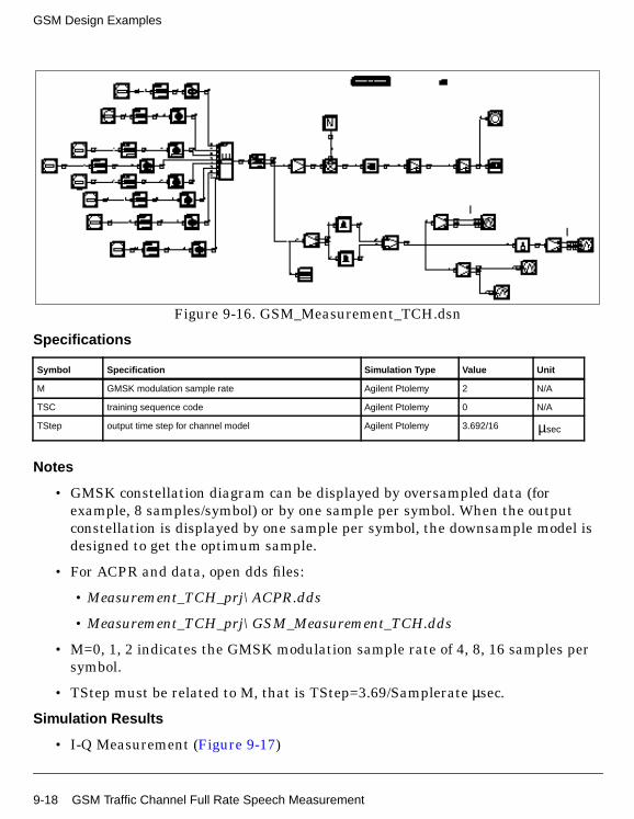
GSM Design Examples
Figure 9-16. GSM_Measurement_TCH.dsn
Specifications
Notes
• GMSK constellation diagram can be displayed by oversampled data (forexample, 8 samples/symbol) or by one sample per symbol. When the outputconstellation is displayed by one sample per symbol, the downsample model isdesigned to get the optimum sample.
• For ACPR and data, open dds files:
• Measurement_TCH_prj\ACPR.dds
• Measurement_TCH_prj\GSM_Measurement_TCH.dds
• M=0, 1, 2 indicates the GMSK modulation sample rate of 4, 8, 16 samples persymbol.
• TStep must be related to M, that is TStep=3.69/Samplerate µsec.
Simulation Results
• I-Q Measurement (Figure 9-17)
Symbol Specification Simulation Type Value Unit
M GMSK modulation sample rate Agilent Ptolemy 2 N/A
TSC training sequence code Agilent Ptolemy 0 N/A
TStep output time step for channel model Agilent Ptolemy 3.692/16 µsec
9-18 GSM Traffic Channel Full Rate Speech Measurement
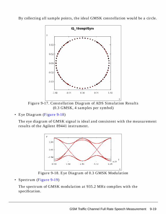
By collecting all sample points, the ideal GMSK constellation would be a circle.
Figure 9-17. Constellation Diagram of ADS Simulation Results(0.3 GMSK, 4 samples per symbol)
• Eye Diagram (Figure 9-18)
The eye diagram of GMSK signal is ideal and consistent with the measurementresults of the Agilent 89441 instrument.
Figure 9-18. Eye Diagram of 0.3 GMSK Modulation
• Spectrum (Figure 9-19)
The spectrum of GMSK modulation at 935.2 MHz complies with thespecification.
GSM Traffic Channel Full Rate Speech Measurement 9-19
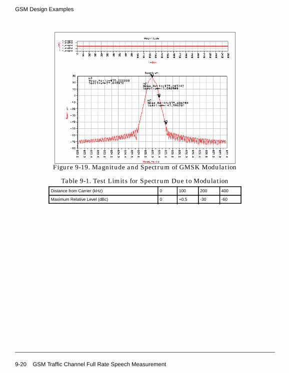
GSM Design Examples
Figure 9-19. Magnitude and Spectrum of GMSK Modulation
Table 9-1. Test Limits for Spectrum Due to ModulationDistance from Carrier (kHz) 0 100 200 400
Maximum Relative Level (dBc) 0 +0.5 -30 -60
9-20 GSM Traffic Channel Full Rate Speech Measurement
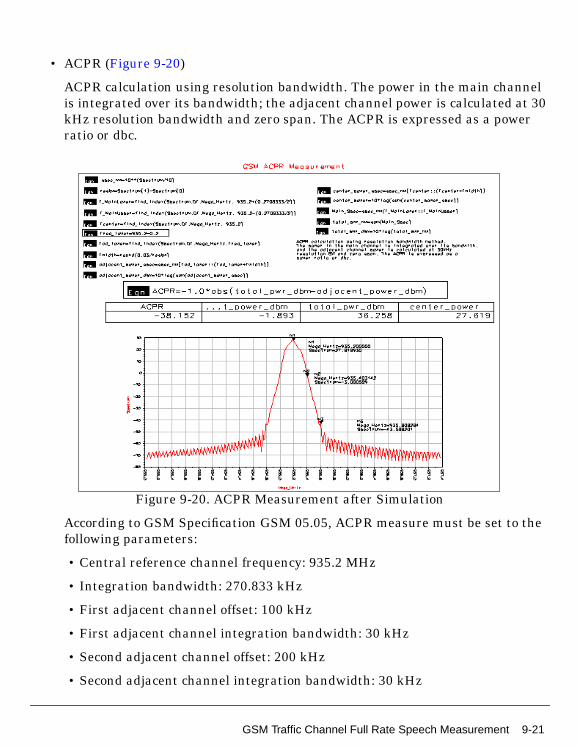
• ACPR (Figure 9-20)
ACPR calculation using resolution bandwidth. The power in the main channelis integrated over its bandwidth; the adjacent channel power is calculated at 30kHz resolution bandwidth and zero span. The ACPR is expressed as a powerratio or dbc.
Figure 9-20. ACPR Measurement after Simulation
According to GSM Specification GSM 05.05, ACPR measure must be set to thefollowing parameters:
• Central reference channel frequency: 935.2 MHz
• Integration bandwidth: 270.833 kHz
• First adjacent channel offset: 100 kHz
• First adjacent channel integration bandwidth: 30 kHz
• Second adjacent channel offset: 200 kHz
• Second adjacent channel integration bandwidth: 30 kHz
GSM Traffic Channel Full Rate Speech Measurement 9-21
GSM Design Examples
• Third adjacent channel offset: 400 kHz
• Third adjacent channel integration bandwidth: 30 kHz
Benchmark
• Hardware platform: Pentium Pro 200 MHz, 96 MB memory
• Software platform: Windows NT 4.0 Workstation, Advanced Design System 1.1
• Data points: 2496 frames
• Simulation time: approximately 90 seconds
Table 9-2. Summary of Agilent GSM-ESG Link ACPR Performanceversus ETSI GSM 05.05 Recommendations
Offset from carrier (kHz) 200 400 600 1200
ETSI spec (dBc) -30 -60 -70 -73
Agilent Advanced Design System simulationresults (dBc)
-35 -77 -95 -102
9-22 GSM Traffic Channel Full Rate Speech Measurement

Random Access ChannelRACHsys_prj Design Names
• GSM_RACH.dsn
Features
• GSM propagation fading channel and additive white Gaussian noise
• Random access channel
• GMSK modulator and MLSE equalizer
• Gaussian noise with adjustable noise variance
• BER and FER performance stored in NumericSink
Description
This example shows the system performance of BER and FER on random accesschannel. It consists of error correction coding and decoding, data framing anddeframing, GMSK modulation, GSM fading channel plus additive white Gaussiannoise, 7-order Butterworth filter, bit synchronization and maximum-likelihoodsequence estimation receiver.
In random access channel, a cyclic code and a convolutional code with tail bits areused; interleaving models are not used. Each 8 data bits are transformed into 36 bitsafter channel coding.
For details about framing, GMSK modulation, synchronization and MLSE reception,refer to Traffic Channel for Data Transmission at 9.6 kbps.
Schematics
Figure 9-21 shows the schematic for this design. The data source is a random bitsequence (B1). Figure 9-22 is the GSM_RACH_Encoder subnetwork used inFigure 9-21. The number of input and output bits of cyclic encoder are 8 and 14,respectively; 4 tail bits are added to the cyclic coded data. These 18 bits areconvolutionally encoded to 36 bits with constraint length of 5 and rate of 1/2.Figure 9-23 shows the GSM_RACH_Decoder subnetwork.
Random Access Channel 9-23
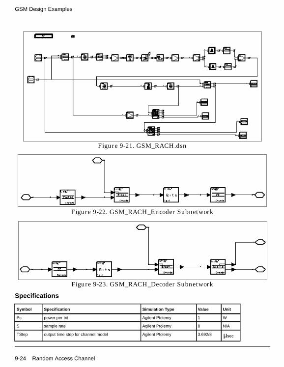
GSM Design Examples
Figure 9-21. GSM_RACH.dsn
Figure 9-22. GSM_RACH_Encoder Subnetwork
Figure 9-23. GSM_RACH_Decoder Subnetwork
Specifications
Symbol Specification Simulation Type Value Unit
Pc power per bit Agilent Ptolemy 1 W
S sample rate Agilent Ptolemy 8 N/A
TStep output time step for channel model Agilent Ptolemy 3.692/8 µsec
9-24 Random Access Channel

Notes
• TStep must be related to S, that is TStep=3.69/SampleRate µsec.
Simulation Results
Figure 9-24 shows the bit error with and without channel coding. The BERperformance of the system with channel coding is much better than the BERperformance without channel coding.
Figure 9-24. BER Performance of Random Access Channel System
Benchmark
• Hardware platform: Pentium Pro 200 MHz, 96 MB memory
• Software platform: Windows NT 4.0 Workstation, Advanced Design System 1.1
• Data points: 6000 frames
• Simulation time: approximately 8 hours
without channel codingwithout channel coding
with channel codingwith channel coding
Random Access Channel 9-25
GSM Design Examples
Slow Associated Control ChannelSACCHsys_prj Design Name
• GSM_SysSACCH.dsn
Features
• GSM propagation fading channel and additive white Gaussian noise
• Slow associated control channel
• Channel interleaving and de-interleaving
• GMSK modulator and MLSE equalizer
• Gaussian noise with adjustable noise variance
• BER and FER performance stored in NumericSink
Description
This example shows the system performance of BER and FER on slow associatedcontrol channel. It consists of error correction coding and decoding, interleaving andde-interleaving, data framing and deframing, GMSK modulation, GSM fadingchannel plus additive white Gaussian noise, 7-order Butterworth filter, bitsynchronization and maximum-likelihood sequence estimation receiver.
In the slow associated control channel, a Fire code with tail bits, a convolutional codeand block rectangular interleaver are used. Each 184 data bits are transformed into456 bits after channel coding and interleaving.
For details about framing, GMSK modulation, synchronization and MLSE reception,refer to Traffic Channel for Data Transmission at 9.6 kbps.
Schematics
Figure 9-25 shows the BER and FER measurement for SACCH transmission andreception. Data source is a random bit sequence (B1). Figure 9-26 is theGSM_SACCH_Encoder sub-network used in Figure 9-25 (detailed implementation ofchannel coding and interleaving for the slow associated control channel). The numberof input and output bits of cyclic encoder are 184 and 224, respectively; 4 tail bits areadded to the cyclic coded data. These 228 bits are convolutionally encoded to 456 bitswith constraint length of 5 and rate of 1/2. GSM_Interleaver_4 is used to interleavethe input 456 bits into four blocks.
Figure 9-27 shows the GSM_SACCH_Decoder subnetwork.
9-26 Slow Associated Control Channel

Figure 9-25. GSM_SysSACCH.dsn
Figure 9-26. GSM_SACCH_Encoder Subnetwork
Figure 9-27. GSM_SACCH_Decoder Subnetwork
Specifications
Symbol Specification Simulation Type Value Unit
Pc power per bit Agilent Ptolemy 1e-3 W
SampleRate sample rate Agilent Ptolemy 8 N/A
TStep output time step for channel model Agilent Ptolemy 3.692/8 µsec
Slow Associated Control Channel 9-27
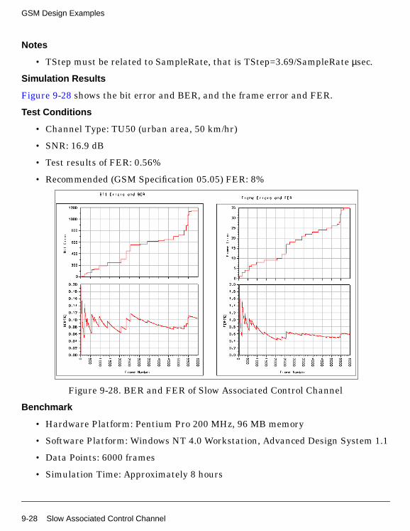
GSM Design Examples
Notes
• TStep must be related to SampleRate, that is TStep=3.69/SampleRate µsec.
Simulation Results
Figure 9-28 shows the bit error and BER, and the frame error and FER.
Test Conditions
• Channel Type: TU50 (urban area, 50 km/hr)
• SNR: 16.9 dB
• Test results of FER: 0.56%
• Recommended (GSM Specification 05.05) FER: 8%
Figure 9-28. BER and FER of Slow Associated Control Channel
Benchmark
• Hardware Platform: Pentium Pro 200 MHz, 96 MB memory
• Software Platform: Windows NT 4.0 Workstation, Advanced Design System 1.1
• Data Points: 6000 frames
• Simulation Time: Approximately 8 hours
9-28 Slow Associated Control Channel
Synchronization ChannelSCHsys_prj Design Name
• GSM_SysSCH.dsn
Features
• GSM propagation fading channel and additive white Gaussian noise
• Synchronization channel
• GMSK modulator and MLSE equalizer
• Gaussian noise with adjustable noise variance
• BER and FER performance stored in NumericSink
Description
This example shows the system performance of BER and FER on synchronizationchannel. It consists of error correction coding and de-interleaving, data framing anddeframing, GMSK modulation, GSM fading channel plus additive white Gaussiannoise, 7-order Butterworth filter, bit synchronization and maximum-likelihoodsequence estimation receiver.
In the synchronization channel, a cyclic code and a convolutional code with tail bitsare used; interleaving models are not used. Each 25 data bits are transformed into 78bits after channel coding.
For details about framing, GMSK modulation, synchronization and MLSE reception,refer to Traffic Channel for Data Transmission at 9.6 kbps.
Schematics
Figure 9-29 shows the schematic design of BER and FER measurement for thesynchronization channel transmission and reception. Data source is a random bitsequence (B1).
Figure 9-30 is the sub-network GSM_SCH_Encoder used in Figure 9-29 (detailedimplementation of channel coding for SCH). The number of input and output bits ofcyclic encoder are 25 and 35, respectively; 4 tail bits are added to the cyclic codeddata. These 39 bits are convolutionally encoded to 78 bits with constraint length of 5and rate of 1/2. (Interleaving models are not used in SCH encoding.)
Figure 9-31 shows the implementation of GSM synchronization channel decoder.
Synchronization Channel 9-29

GSM Design Examples
Figure 9-29. GSM_SysSCH.dsn
Figure 9-30. GSM_SCH_Encoder Subnetwork
Figure 9-31. GSM_SCH_Decoder Subnetwork
Specifications
Symbol Specification Simulation Type Value Unit
GlobalPc power per bit Agilent Ptolemy 1e-3 W
FCarrier carrier frequency Agilent Ptolemy 900 MHz
SR sample rate Agilent Ptolemy 8 N/A
TStep output time step for channel model Agilent Ptolemy 3.692/8 µsec
9-30 Synchronization Channel
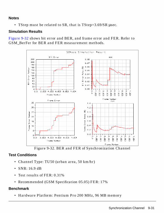
Notes
• TStep must be related to SR, that is TStep=3.69/SR µsec.
Simulation Results
Figure 9-32 shows bit error and BER, and frame error and FER. Refer toGSM_BerFer for BER and FER measurement methods.
Figure 9-32. BER and FER of Synchronization Channel
Test Conditions
• Channel Type: TU50 (urban area, 50 km/hr)
• SNR: 16.9 dB
• Test results of FER: 0.31%
• Recommended (GSM Specification 05.05) FER: 17%
Benchmark
• Hardware Platform: Pentium Pro 200 MHz, 96 MB memory
Synchronization Channel 9-31

GSM Design Examples
• Software Platform: Windows NT 4.0 Workstation, Advanced Design System 1.1
• Data Points: 10000 frames
• Simulation Time: approximately 16 hours
9-32 Synchronization Channel

Traffic Channel for Data Transmission at 2.4 kbpsTCH24Sys_prj Design Name
• GSM_Sys_TCH24.dsn
Features
• GSM propagation fading channel and additive white Gaussian noise
• Channel codec type: TCH 2.4 kbps
• Channel interleaving and de-interleaving
• GMSK modulator and maximum-likelihood sequence estimation equalizer
• Gaussian noise with adjustable noise variance
• BER and FER performance stored in NumericSink
Description
This example shows the system performance of BER and FER on 2.4 kbps full-ratetraffic channel (TCH/F2.4). It consists of error correction coding and decoding,interleaving and de-interleaving, data framing and deframing, GMSK modulation,GSM fading channel and additive white Gaussian noise channel, 7-orderButterworth filter, bit synchronization and maximum-likelihood sequence estimationreceiver.
In transmission of TCH/F2.4, only a convolutional code with tail bits is used withblock diagonal interleaving. Each 72 data bits are transformed into 456 bits afterchannel coding.
For details about framing, GMSK modulation, synchronization and MLSE reception,refer to Traffic Channel for Data Transmission at 9.6 kbps.
Schematics
Figure 9-33 shows the schematic for this design. The data source is a random bitsequence (B1).
Figure 9-34 is the GSM_TCHF24_Encoder sub-network used in Figure 9-33, i.e.,detailed implementation of channel coding and interleaving for TCH 2.4kbps. Foreach 72 data bits input, 4 tail bits are added. These 76 bits are convolutionallyencoded to 456 bits with constraint length of 5 and rate of 1/6. The 456 coded bits areblock diagonal interleaved over 8 blocks. And after interleaving and insertingstealing flag bits, 464 bits are produced.
Traffic Channel for Data Transmission at 2.4 kbps 9-33
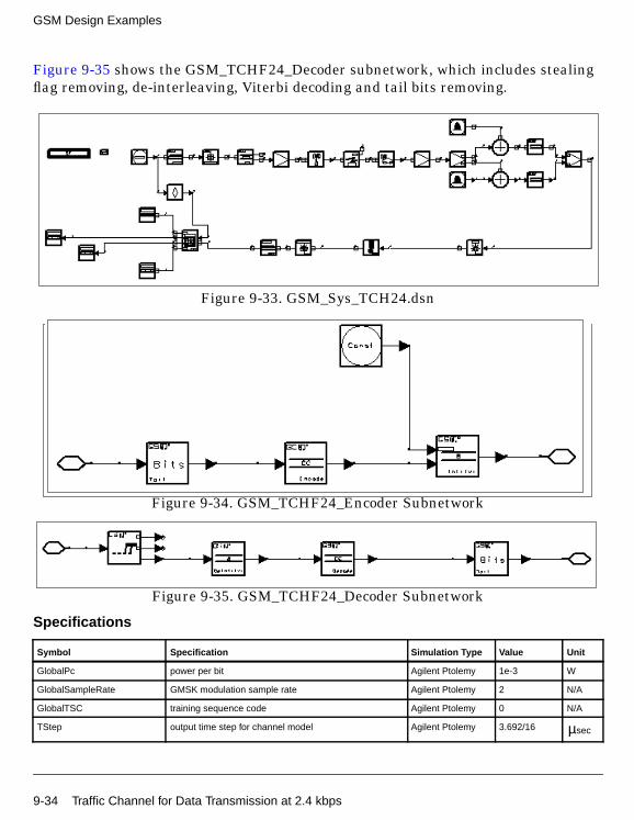
GSM Design Examples
Figure 9-35 shows the GSM_TCHF24_Decoder subnetwork, which includes stealingflag removing, de-interleaving, Viterbi decoding and tail bits removing.
Figure 9-33. GSM_Sys_TCH24.dsn
Figure 9-34. GSM_TCHF24_Encoder Subnetwork
Figure 9-35. GSM_TCHF24_Decoder Subnetwork
Specifications
Symbol Specification Simulation Type Value Unit
GlobalPc power per bit Agilent Ptolemy 1e-3 W
GlobalSampleRate GMSK modulation sample rate Agilent Ptolemy 2 N/A
GlobalTSC training sequence code Agilent Ptolemy 0 N/A
TStep output time step for channel model Agilent Ptolemy 3.692/16 µsec
9-34 Traffic Channel for Data Transmission at 2.4 kbps
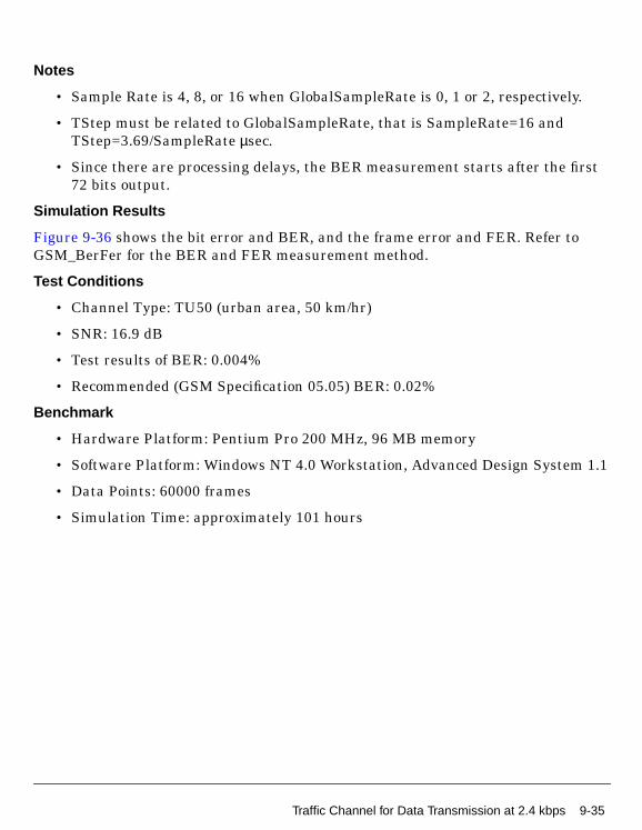
Notes
• Sample Rate is 4, 8, or 16 when GlobalSampleRate is 0, 1 or 2, respectively.
• TStep must be related to GlobalSampleRate, that is SampleRate=16 andTStep=3.69/SampleRate µsec.
• Since there are processing delays, the BER measurement starts after the first72 bits output.
Simulation Results
Figure 9-36 shows the bit error and BER, and the frame error and FER. Refer toGSM_BerFer for the BER and FER measurement method.
Test Conditions
• Channel Type: TU50 (urban area, 50 km/hr)
• SNR: 16.9 dB
• Test results of BER: 0.004%
• Recommended (GSM Specification 05.05) BER: 0.02%
Benchmark
• Hardware Platform: Pentium Pro 200 MHz, 96 MB memory
• Software Platform: Windows NT 4.0 Workstation, Advanced Design System 1.1
• Data Points: 60000 frames
• Simulation Time: approximately 101 hours
Traffic Channel for Data Transmission at 2.4 kbps 9-35
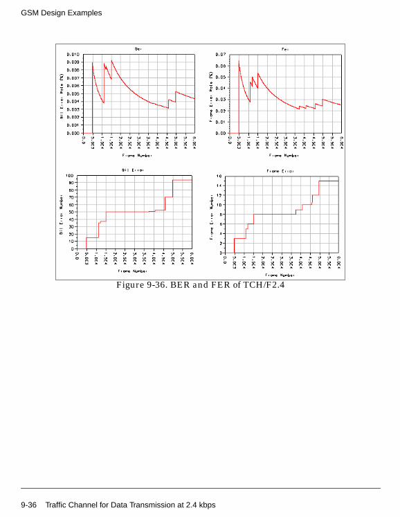
GSM Design Examples
Figure 9-36. BER and FER of TCH/F2.4
9-36 Traffic Channel for Data Transmission at 2.4 kbps
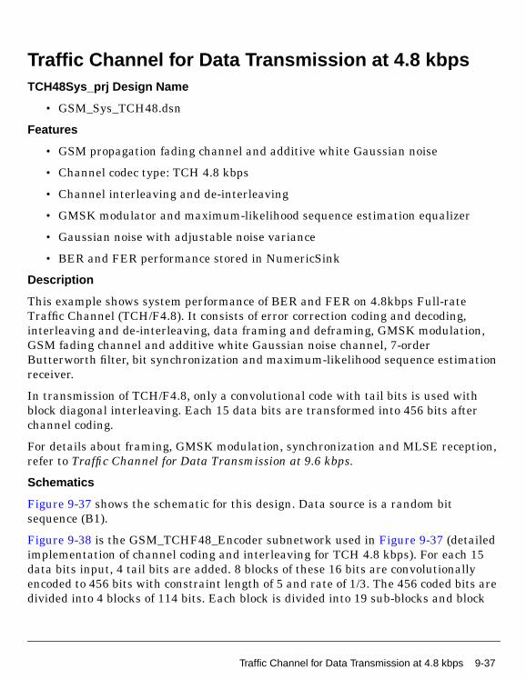
Traffic Channel for Data Transmission at 4.8 kbpsTCH48Sys_prj Design Name
• GSM_Sys_TCH48.dsn
Features
• GSM propagation fading channel and additive white Gaussian noise
• Channel codec type: TCH 4.8 kbps
• Channel interleaving and de-interleaving
• GMSK modulator and maximum-likelihood sequence estimation equalizer
• Gaussian noise with adjustable noise variance
• BER and FER performance stored in NumericSink
Description
This example shows system performance of BER and FER on 4.8kbps Full-rateTraffic Channel (TCH/F4.8). It consists of error correction coding and decoding,interleaving and de-interleaving, data framing and deframing, GMSK modulation,GSM fading channel and additive white Gaussian noise channel, 7-orderButterworth filter, bit synchronization and maximum-likelihood sequence estimationreceiver.
In transmission of TCH/F4.8, only a convolutional code with tail bits is used withblock diagonal interleaving. Each 15 data bits are transformed into 456 bits afterchannel coding.
For details about framing, GMSK modulation, synchronization and MLSE reception,refer to Traffic Channel for Data Transmission at 9.6 kbps.
Schematics
Figure 9-37 shows the schematic for this design. Data source is a random bitsequence (B1).
Figure 9-38 is the GSM_TCHF48_Encoder subnetwork used in Figure 9-37 (detailedimplementation of channel coding and interleaving for TCH 4.8 kbps). For each 15data bits input, 4 tail bits are added. 8 blocks of these 16 bits are convolutionallyencoded to 456 bits with constraint length of 5 and rate of 1/3. The 456 coded bits aredivided into 4 blocks of 114 bits. Each block is divided into 19 sub-blocks and block
Traffic Channel for Data Transmission at 4.8 kbps 9-37
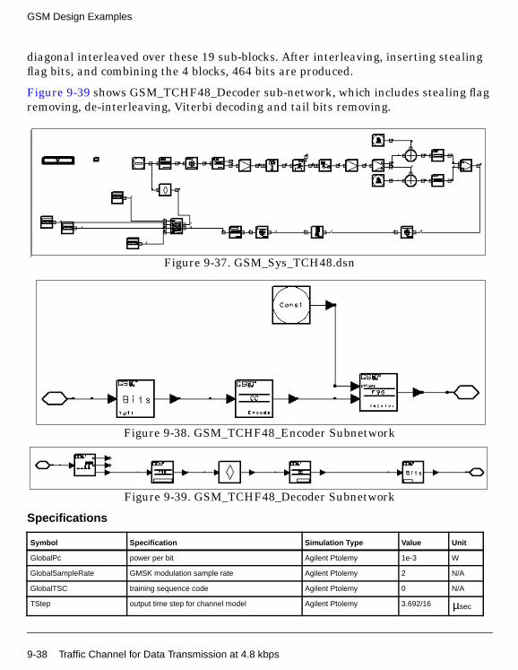
GSM Design Examples
diagonal interleaved over these 19 sub-blocks. After interleaving, inserting stealingflag bits, and combining the 4 blocks, 464 bits are produced.
Figure 9-39 shows GSM_TCHF48_Decoder sub-network, which includes stealing flagremoving, de-interleaving, Viterbi decoding and tail bits removing.
Figure 9-37. GSM_Sys_TCH48.dsn
Figure 9-38. GSM_TCHF48_Encoder Subnetwork
Figure 9-39. GSM_TCHF48_Decoder Subnetwork
Specifications
Symbol Specification Simulation Type Value Unit
GlobalPc power per bit Agilent Ptolemy 1e-3 W
GlobalSampleRate GMSK modulation sample rate Agilent Ptolemy 2 N/A
GlobalTSC training sequence code Agilent Ptolemy 0 N/A
TStep output time step for channel model Agilent Ptolemy 3.692/16 µsec
9-38 Traffic Channel for Data Transmission at 4.8 kbps
Notes
• Sample Rate is 4, 8, 16 when parameter GlobalSampleRate is 0, 1 or 2,respectively.
• TStep must be related to GlobalSampleRate, that is SampleRate=16 andTStep=3.69/SampleRate µsec.
• Since there are processing delays, the BER measurement starts after first 600bits output.
Simulation Results
Figure 9-40 shows the bit error and BER, and the frame error and FER. Refer toGSM_BerFer for the BER and FER measurement method.
Test Conditions
• Channel Type: HT100 (hilly terrain, 100 km/hr)
• SNR: 14 dB
• Test results of BER: 0.009%
• Recommended (GSM Specification 05.05) BER: 0.01%
Benchmark
• Hardware Platform: Pentium Pro 200MHz, 96 MB memory
• Software Platform: Windows NT 4.0 Workstation, Advanced Design System 1.1
• Data Points: 20000 frames
• Simulation Time: approximately 32 hours
Traffic Channel for Data Transmission at 4.8 kbps 9-39
GSM Design Examples
Figure 9-40. BER and FER of TCH/F4.8
9-40 Traffic Channel for Data Transmission at 4.8 kbps
Traffic Channel for Data Transmission at 9.6 kbpsTCH96Sys_prj Design Name
• GSM_Sys_TCH96.dsn
Features
• GSM propagation fading channel and additive white Gaussian noise
• Channel codec type: TCH/F9.6
• Channel interleaving and de-interleaving
• GMSK modulator and maximum-likelihood sequence estimation equalizer
• Gaussian noise with adjustable noise variance
• BER and FER performance stored in NumericSink
Description
This example shows the system performance of BER and FER on 9.6 kbps full-ratetraffic channel (TCH/F9.6). It consists of error correction coding and decoding,interleaving and de-interleaving, data framing and deframing, GMSK modulation,GSM channel, 7-order Butterworth filter, bit synchronization, maximum-likelihoodsequence estimation receiver.
The system source is a random bit source. Input data is convolutionally coded at rate1/2, interleaved, and fed into a normal burst construction component. After trainingsequence, tail bits and guard time bits are added, data is placed in a GMSKmodulation model. In this example only one user is considered. The channel containspropagation fading channel and additive white Gaussian noise channel. 12 channeltypes can be selected with adjustable parameters such as velocity, antenna height,and location.
In the receiver, the signal is filtered by 7-order Butterworth filter (designed by theDSP Filter Designer of Agilent Advanced Design System). The bit synchronizationmodel is designed to select the optimum sample in a symbol that is transferred to anMLSE receiver. After signal recovery in the maximum-likelihood sequence estimationreceiver, burst disassembly, de-interleaving and channel decoding, the system BERand FER are measured.
Schematics
Figure 9-41 shows the schematic for this design. Data source is a random bitsequence (B1).
Traffic Channel for Data Transmission at 9.6 kbps 9-41
GSM Design Examples
Figure 9-42 shows the GSM_TCHF96_Encoder subnetwork used in Figure 9-41(detailed implementation of channel coding and interleaving of traffic channel fordata transmission at 9.6 kbps). For each 240 data bits input, 4 tail bits are added.These 244 bits are convolutionally encoded to 488 bits with constraint length of 5 andrate of 1/2; 32 of the 488 coded bits are punctured. The remaining 456 bits are firstdivided into four 114-bit length blocks. Each block is then divided into 19 sub-blocksand block diagonal interleaved over these 19 sub-blocks. After interleaving, insertingstealing flag bits and combining the 4 blocks, 464 bits are produced.
Figure 9-41. GSM_Sys_TCH96.dsn
Figure 9-42. GSM_TCHF96_Encoder Subnetwork
9-42 Traffic Channel for Data Transmission at 9.6 kbps
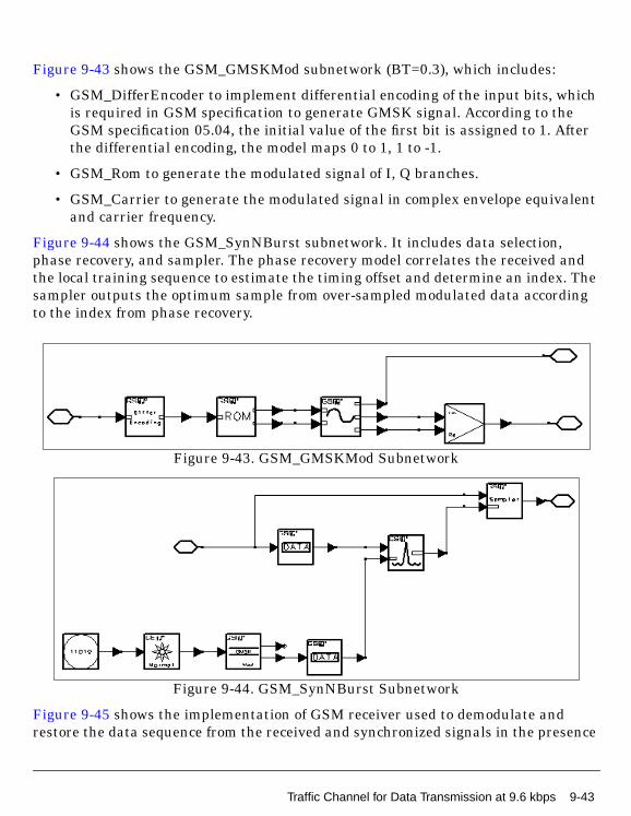
Figure 9-43 shows the GSM_GMSKMod subnetwork (BT=0.3), which includes:
• GSM_DifferEncoder to implement differential encoding of the input bits, whichis required in GSM specification to generate GMSK signal. According to theGSM specification 05.04, the initial value of the first bit is assigned to 1. Afterthe differential encoding, the model maps 0 to 1, 1 to -1.
• GSM_Rom to generate the modulated signal of I, Q branches.
• GSM_Carrier to generate the modulated signal in complex envelope equivalentand carrier frequency.
Figure 9-44 shows the GSM_SynNBurst subnetwork. It includes data selection,phase recovery, and sampler. The phase recovery model correlates the received andthe local training sequence to estimate the timing offset and determine an index. Thesampler outputs the optimum sample from over-sampled modulated data accordingto the index from phase recovery.
Figure 9-43. GSM_GMSKMod Subnetwork
Figure 9-44. GSM_SynNBurst Subnetwork
Figure 9-45 shows the implementation of GSM receiver used to demodulate andrestore the data sequence from the received and synchronized signals in the presence
Traffic Channel for Data Transmission at 9.6 kbps 9-43
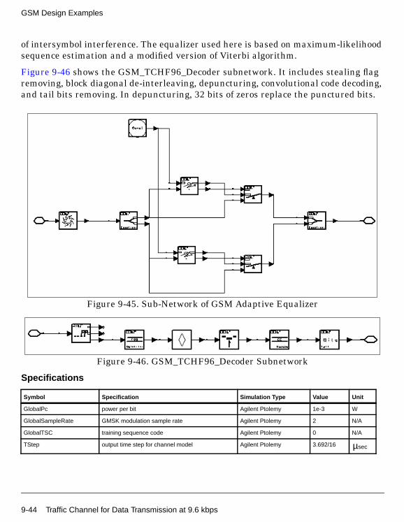
GSM Design Examples
of intersymbol interference. The equalizer used here is based on maximum-likelihoodsequence estimation and a modified version of Viterbi algorithm.
Figure 9-46 shows the GSM_TCHF96_Decoder subnetwork. It includes stealing flagremoving, block diagonal de-interleaving, depuncturing, convolutional code decoding,and tail bits removing. In depuncturing, 32 bits of zeros replace the punctured bits.
Figure 9-45. Sub-Network of GSM Adaptive Equalizer
Figure 9-46. GSM_TCHF96_Decoder Subnetwork
Specifications
Symbol Specification Simulation Type Value Unit
GlobalPc power per bit Agilent Ptolemy 1e-3 W
GlobalSampleRate GMSK modulation sample rate Agilent Ptolemy 2 N/A
GlobalTSC training sequence code Agilent Ptolemy 0 N/A
TStep output time step for channel model Agilent Ptolemy 3.692/16 µsec
9-44 Traffic Channel for Data Transmission at 9.6 kbps
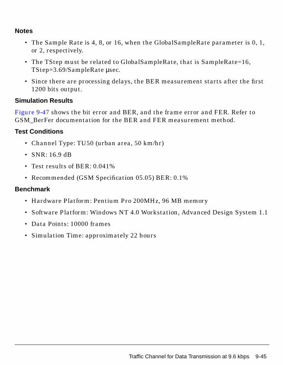
Notes
• The Sample Rate is 4, 8, or 16, when the GlobalSampleRate parameter is 0, 1,or 2, respectively.
• The TStep must be related to GlobalSampleRate, that is SampleRate=16,TStep=3.69/SampleRate µsec.
• Since there are processing delays, the BER measurement starts after the first1200 bits output.
Simulation Results
Figure 9-47 shows the bit error and BER, and the frame error and FER. Refer toGSM_BerFer documentation for the BER and FER measurement method.
Test Conditions
• Channel Type: TU50 (urban area, 50 km/hr)
• SNR: 16.9 dB
• Test results of BER: 0.041%
• Recommended (GSM Specification 05.05) BER: 0.1%
Benchmark
• Hardware Platform: Pentium Pro 200MHz, 96 MB memory
• Software Platform: Windows NT 4.0 Workstation, Advanced Design System 1.1
• Data Points: 10000 frames
• Simulation Time: approximately 22 hours
Traffic Channel for Data Transmission at 9.6 kbps 9-45

GSM Design Examples
Figure 9-47. BER and FER of TCH/F9.6 System
9-46 Traffic Channel for Data Transmission at 9.6 kbps
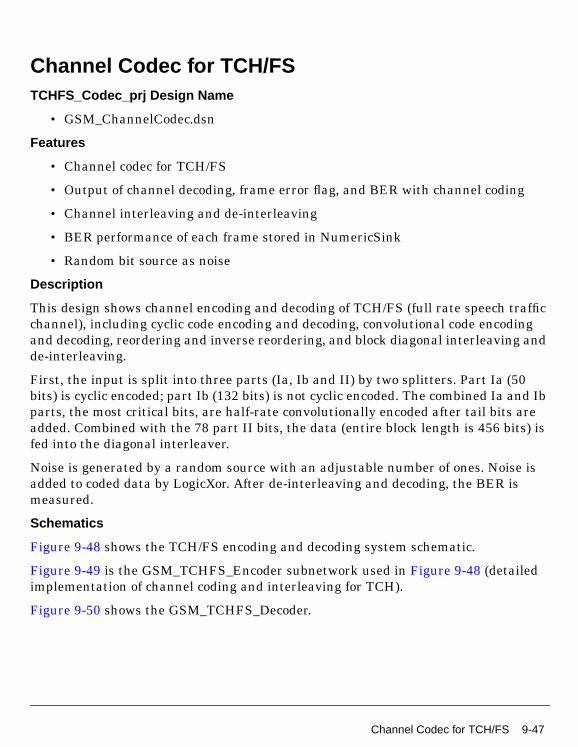
Channel Codec for TCH/FSTCHFS_Codec_prj Design Name
• GSM_ChannelCodec.dsn
Features
• Channel codec for TCH/FS
• Output of channel decoding, frame error flag, and BER with channel coding
• Channel interleaving and de-interleaving
• BER performance of each frame stored in NumericSink
• Random bit source as noise
Description
This design shows channel encoding and decoding of TCH/FS (full rate speech trafficchannel), including cyclic code encoding and decoding, convolutional code encodingand decoding, reordering and inverse reordering, and block diagonal interleaving andde-interleaving.
First, the input is split into three parts (Ia, Ib and II) by two splitters. Part Ia (50bits) is cyclic encoded; part Ib (132 bits) is not cyclic encoded. The combined Ia and Ibparts, the most critical bits, are half-rate convolutionally encoded after tail bits areadded. Combined with the 78 part II bits, the data (entire block length is 456 bits) isfed into the diagonal interleaver.
Noise is generated by a random source with an adjustable number of ones. Noise isadded to coded data by LogicXor. After de-interleaving and decoding, the BER ismeasured.
Schematics
Figure 9-48 shows the TCH/FS encoding and decoding system schematic.
Figure 9-49 is the GSM_TCHFS_Encoder subnetwork used in Figure 9-48 (detailedimplementation of channel coding and interleaving for TCH).
Figure 9-50 shows the GSM_TCHFS_Decoder.
Channel Codec for TCH/FS 9-47
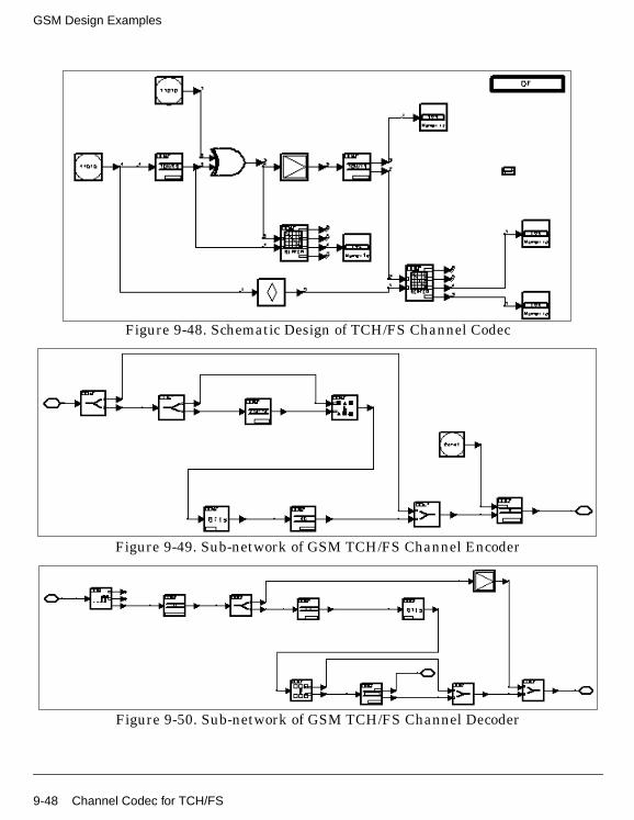
GSM Design Examples
Figure 9-48. Schematic Design of TCH/FS Channel Codec
Figure 9-49. Sub-network of GSM TCH/FS Channel Encoder
Figure 9-50. Sub-network of GSM TCH/FS Channel Decoder
9-48 Channel Codec for TCH/FS
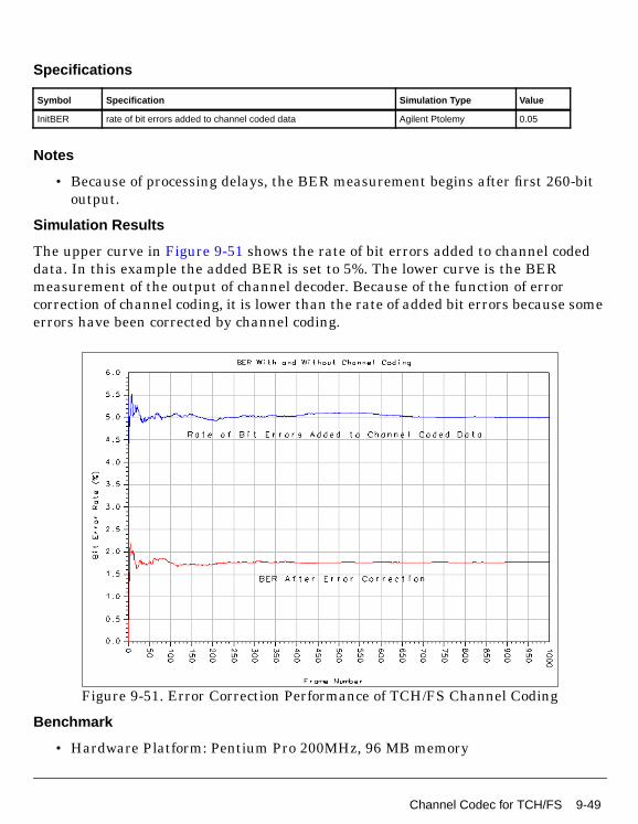
Specifications
Notes
• Because of processing delays, the BER measurement begins after first 260-bitoutput.
Simulation Results
The upper curve in Figure 9-51 shows the rate of bit errors added to channel codeddata. In this example the added BER is set to 5%. The lower curve is the BERmeasurement of the output of channel decoder. Because of the function of errorcorrection of channel coding, it is lower than the rate of added bit errors because someerrors have been corrected by channel coding.
Figure 9-51. Error Correction Performance of TCH/FS Channel Coding
Benchmark
• Hardware Platform: Pentium Pro 200MHz, 96 MB memory
Symbol Specification Simulation Type Value
InitBER rate of bit errors added to channel coded data Agilent Ptolemy 0.05
Channel Codec for TCH/FS 9-49

GSM Design Examples
• Software Platform: Windows NT 4.0 Workstation, Advanced Design System 1.1
• Data Points: 1000 frames
• Simulation Time: approximately 1 minute
9-50 Channel Codec for TCH/FS

Transmission and Reception of TrafficChannel/Full-Rate SpeechTCHFSsys_prj Design Name
• GSM_TCHFS.dsn
Features
• Displays output of channel decoding, frame error flag, and BER with andwithout channel coding
• Fading channel with additive white Gaussian noise
• Adaptive equalizer using maximum-likelihood sequence estimation
• Bit synchronization using correlation method
• BER of each frame stored in NumericSink
Description
This example demonstrates transmission and reception of traffic channel/full-ratespeech (TCH/FS). The type of the burst in this example is normal burst. A random bitsource component is used as a full rate (13 kbps) speech data source.
Transmission includes channel coding, normal burst construction, and GMSKmodulation. Channel coding for TCH/FS includes a cyclic encoder, a convolutionalcode encoder, a channel interleaver and a re-orderer, two splitters that split inputdata into blocks of different classes, and a combiner that combines these blocks aftercoding. Before passing channel, a GMSK modulator is applied. The channel used is aGSM propagation fading channel. The type of channel, path loss, height of antenna,gain of antenna, position and speed of the mobile station are user-settableparameters. A Gaussian noise in complex envelope is added to the received signal.
The receiver includes a Butterworth filter, a normal burst synchronizer, anequalization receiver, normal burst disassembly, and a channel decoder. Theequalization receiver is an adaptive equalizer that uses maximum-likelihoodsequence estimation. The channel decoder includes a channel de-interleaver,decoders for convolutional and cyclic code, a splitter, and a combiner.
The BER of channel coded data is measured and compared to data without channelcoding.
Schematics
Transmission and Reception of Traffic Channel/Full-Rate Speech 9-51
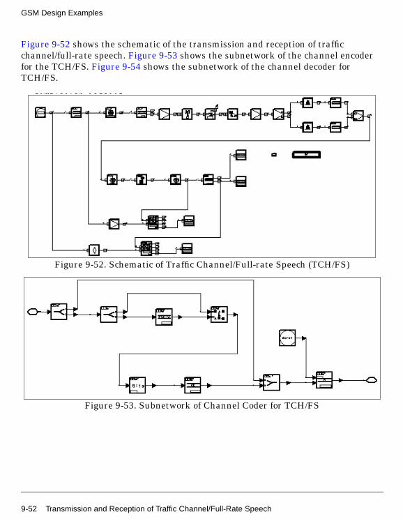
GSM Design Examples
Figure 9-52 shows the schematic of the transmission and reception of trafficchannel/full-rate speech. Figure 9-53 shows the subnetwork of the channel encoderfor the TCH/FS. Figure 9-54 shows the subnetwork of the channel decoder forTCH/FS.
Figure 9-52. Schematic of Traffic Channel/Full-rate Speech (TCH/FS)
Figure 9-53. Subnetwork of Channel Coder for TCH/FS
9-52 Transmission and Reception of Traffic Channel/Full-Rate Speech
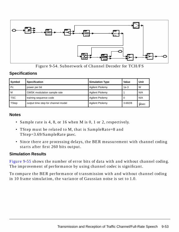
Figure 9-54. Subnetwork of Channel Decoder for TCH/FS
Specifications
Notes
• Sample rate is 4, 8, or 16 when M is 0, 1 or 2, respectively.
• TStep must be related to M, that is SampleRate=8 andTStep=3.69/SampleRate µsec.
• Since there are processing delays, the BER measurement with channel codingstarts after first 260 bits output.
Simulation Results
Figure 9-55 shows the number of error bits of data with and without channel coding.The improvement of performance by using channel codec is significant.
To compare the BER performance of transmission with and without channel codingin 10 frame simulation, the variance of Gaussian noise is set to 1.0.
Symbol Specification Simulation Type Value Unit
Pc power per bit Agilent Ptolemy 1e-3 W
M GMSK modulation sample rate Agilent Ptolemy 1 N/A
TSC training sequence code Agilent Ptolemy 0 N/A
TStep output time step for channel model Agilent Ptolemy 3.692/8 µsec
Transmission and Reception of Traffic Channel/Full-Rate Speech 9-53
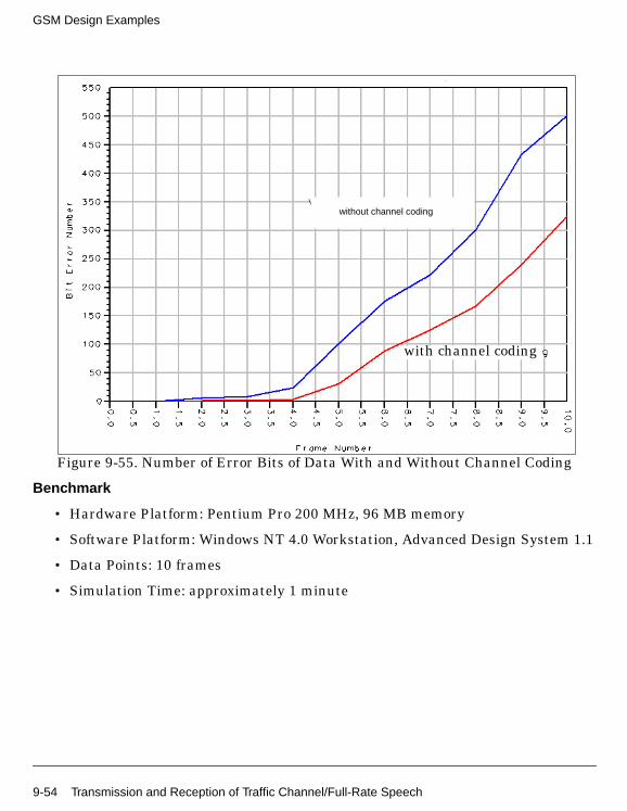
GSM Design Examples
Figure 9-55. Number of Error Bits of Data With and Without Channel Coding
Benchmark
• Hardware Platform: Pentium Pro 200 MHz, 96 MB memory
• Software Platform: Windows NT 4.0 Workstation, Advanced Design System 1.1
• Data Points: 10 frames
• Simulation Time: approximately 1 minute
without channel coding
with channel coding
9-54 Transmission and Reception of Traffic Channel/Full-Rate Speech

Index
GGSM Design Library, 1-1GSM_AccessBurst, 4-2GSM_APCM_Quantizer, 7-2GSM_AQuarterBitAdd, 6-2GSM_AQuarterBitRmv, 6-4GSM_Autocorrelation, 7-4GSM_BcchCcch4SdcchDn, 4-4GSM_BcchCcch4SdcchUp, 4-6GSM_BcchCcchDn, 4-8GSM_BcchCcchUp, 4-10GSM_BerFer, 5-2GSM_BlockCodeRACH, 2-2GSM_Carrier, 6-6GSM_CC_WithTail, 2-3GSM_ChannelEstimator, 3-2GSM_CodeLAR, 7-6GSM_Combiner, 2-5GSM_CycDecoder, 2-7GSM_CycEncoder, 2-10GSM_DataSelection, 8-2GSM_DCC_WithTail, 2-13GSM_DeAccessBurst, 4-12GSM_DeBcchCcch4SdcchDn, 4-14GSM_DeBcchCcch4SdcchUp, 4-16GSM_DeBcchCcchDn, 4-18GSM_DecodeLAR, 7-8GSM_Deemphasis, 7-10GSM_Deframing, 7-12GSM_Deinterleaver_4, 2-15GSM_Deinterleaver_8, 2-16GSM_Deinterleaver_F96, 2-17GSM_DeMultiframe26, 4-20GSM_DeNormalBurst, 4-22GSM_Depuncture, 2-18GSM_Derotator, 3-4GSM_DeSBurst, 4-24GSM_DeSdcch8Dn, 4-26GSM_DeSdcch8Up, 4-28GSM_DeTDMA, 4-30GSM_DifferDecoder, 6-8GSM_DifferEncoder, 6-10GSM_DummyBurst, 4-32GSM_Equalizer, 3-5GSM_EquCombiner, 3-8GSM_EquComposeAB, 3-10GSM_EquDecomposeAB, 3-12GSM_EquSplitter, 3-14GSM_ErrPatternDisplay, 5-4GSM_FACCH_Decoder, 2-19GSM_FACCH_Encoder, 2-21GSM_FBurst, 4-34GSM_Filter, 3-17GSM_FireDecoder, 2-23GSM_Framing, 7-14GSM_GMSKDemod, 6-12GSM_GMSKMod, 6-14GSM_Interleaver_4, 2-25GSM_Interleaver_8, 2-27GSM_Interleaver_F96, 2-29GSM_Interpolation, 7-16GSM_InverseAPCM, 7-18GSM_InverseReord, 2-31GSM_LARToRefCoe, 7-20GSM_LogAreaRatio, 7-22GSM_LongTermAnalysis, 7-24GSM_LongTermSynthesis, 7-26GSM_LTP_Parameter, 7-28GSM_MpyClock, 6-16GSM_Multiframe26, 4-36GSM_NormalBurst, 4-38GSM_OffsetCompensation, 7-30GSM_PhaseRecovery, 8-4GSM_PhsRcvryTrNoMod, 8-6GSM_Postprocessing, 7-32GSM_Preemphasis, 7-34GSM_Puncture, 2-33GSM_RACH_Decoder, 2-34GSM_RACH_Encoder, 2-36GSM_ReadFile, 7-40GSM_Receiver, 3-19GSM_ReceiverAB, 3-22GSM_Reorder, 2-38GSM_RmvStlFlgs, 2-40GSM_Rom, 6-18GSM_RPE_GridPosition, 7-36GSM_RPE_GridSelection, 7-38GSM_SACCH_Decoder, 2-42GSM_SACCH_Encoder, 2-44GSM_Sampler, 8-8
Index-1
GSM_SBurst, 4-40GSM_ScaleInput, 7-41GSM_SCH_Decoder, 2-46GSM_SCH_Encoder, 2-48GSM_Schur, 7-43GSM_Sdcch8Dn, 4-42GSM_Sdcch8Up, 4-44GSM_ShortTermAnalysis, 7-45GSM_ShortTermPredict, 7-47GSM_ShortTermSynthesis, 7-49GSM_SpeechDecoder, 7-51GSM_SpeechEncoder, 7-53GSM_Splitter, 2-50GSM_SynABurst, 8-10GSM_SynNBurst, 8-12GSM_SynNBurstTrNoMod, 8-14GSM_SynSBurst, 8-16GSM_TailBits, 2-52GSM_TCHF24_Decoder, 2-54GSM_TCHF24_Encoder, 2-56GSM_TCHF48_Decoder, 2-58GSM_TCHF48_Encoder, 2-60GSM_TCHF96_Decoder, 2-62GSM_TCHF96_Encoder, 2-64GSM_TCHFS_Decoder, 2-66GSM_TCHFS_Encoder, 2-68GSM_TDMA, 4-46GSM_TimeBaseCounter, 4-48GSM_TrainBitGen, 8-18GSM_WeightingFilter, 7-56GSM_WriteFile, 7-58
Index-2


