H2020-NMBP-2016-721107
GaNonCMOS (Power Conversion Applications)
Program Overview and
focus on 12/24/48V to 1V Voltage regulators
Séamus O’Driscoll
GaNonCMOS
July 2019 1GaN Summer School Ghent

GaNonCMOS Program Introduction
2July 2019 GaN Summer School Ghent

July 2019 GaN Summer School Ghent 3
www.ganoncmos.eu
Market Demand Partners
HPC: Server VR, Multi-Node
Merchant POL, Aerospace,
Automotive:
Today’s 12V to 1V8 Server/PC VRM
Program Scope: GaN in Integration Power Systems
Efficient, Dense, Low Cost
Flexible for Multi-Node, Multi Core, Lower Voltages, SoC Power, Nano-Grid Power
Compatible Input Power and Output Power

July 2019 GaN Summer School Ghent 4
Systems & Demonstrators
Wafer:
GaN Switch:
CMOS Control/Driver:
Embedded Substrate Technology: (Magnetic Devices and Semiconductors)
Voltage Regulator Designs and Advanced Integrated Magnetic Materials/Devices
Reliability & Power System Manufacturing
Hardware Design PartnersFouad Benkhelifa, Richard Reiner,Norbert Fiebig, Marco LiskerGerald Weidinger, Gerald WeisStanislav suchovskiThomas Brunschwiler, Cezar Zota

July 2019 GaN Summer School Ghent 5
GaN Switches in Power Conversion
• CAGR 50-70%, Still low percentage of overall market,…
GaNonCMOS encompasses Discretes (Smart Drivers), Modules & Power ICs
GaNonCMOS will apply to all of these segments

July 2019 GaN Summer School Ghent 6
GaN Application Advantage - Density
https://www.transphormusa.com/en/
Note the lower x-axis limit is usually shown as 50V!
600V Rated Application may employ 100V to 600 V switches depending on topology level count.
1. C. W. Halsted and M. D. Manjrekar, "A Critique of Little Box Challenge Inverter Designs: Breaking from Traditional Design Tradeoffs," in IEEE Power Electronics Magazine, vol. 5, no. 4, pp. 52-60, Dec. 2018.doi: 10.1109/MPEL.2018.2873992
2. https://pilawa.ece.illinois.edu/files/2016/05/Pilawa_PELS_webinar_may_25_2016_FINAL.pdf
2014-2015 Little Box Challenge (LBC) by Google & IEEE - > 215-W/in3 power densities in 1kVA DC-AC inverter- most of the top 16 entries used GaN

July 2019 GaN Summer School Ghent 7
Littlebox Finalist Solutions Illustrate Switch Voltage Rating Options for 1kVA DC-AC Inverter
Taiwan Tech (TT) Basic Full Bridge- this will require >600V rated
GaN switches > DC Link Voltage
7-Level Flying Capacitor (FCML) Inverter with Output “unfolder” used 100V EPC eHEMT devices
- DC Link Voltage is evenly divided across capacitors. Capacitors “break” the switching voltage.
- Effective per-switch frequency is reduced or Inductor V.s reduced600V GaN competes with 100V GaN!

July 2019 GaN Summer School Ghent 8
Commercial 3kW PFC Prototype (Titanium+ 85-264VRMS)
3-Level PFC Implementation using 150V Silicon MOSFETs
• Stacked Switches reduces Conduction & Switching Losses Significantly
• GaN in similar ML design would increase efficiency from 98.1 to ~98.5%?
Diodes are to bypass inrush surge to CBulk
Low Voltage Silicon Switch Stacks and Multi-Level competing with GaN

July 2019 GaN Summer School Ghent 9
Optimised Silicon vs GaN Implementation for 3kW PFC
• Switching leg: 2 x 600V 35mR GaN Transphorm
• Synchronous rectifier: 2 x 14mR 650V SJ MOSFETs
• PFC Inductor volume: 142cm
• Switching leg: 8 x 150V 11mR 150V OptiMOS Infineon
• Synchronous rectifier: 2 x 19mR 650V SJ MOSFETs
• Inductor volume: 35.2cm3 (~ 4 x reduction)
Transphorm GaN 3.3kW PFC: 50kHz Bridgeless 2-
Level
www.icergi.com
ICERGi 3kW PFC: 70kHz Bridgeless 3-Level
Note what 3-L does o Inductor Volume

• GaNonCMOS Program is concentrating on 12V/24V/48V to low output voltage
• Conversion for GP POL, and VRM for HPC.
• HPC may use direct conversion from 48V (Lower DC Distribution Loss)
• Aerospace (24V)
• Automotive (-> 48V)July 2019 GaN Summer School Ghent 10
Low Voltage DC-DC POL Focus

July 2019 GaN Summer School Ghent 11
Some Switch-Mode Converter Operating Concepts and Loss Mechanisms

July 2019 GaN Summer School Ghent 12
Basic Switching Loss Concepts
• Hard Switching• Coss, 3rd Quadrant Conduction Recovery, Egt
(gate total energy) and VI overlap feature.
• Resonant Valley – Coss (Vds), Egt
• Soft Switching • ZVS – turn on at zero voltage
• ZCS – turn off at zero current

July 2019 GaN Summer School Ghent 13
Continuous Conduction Mode (CCM)Basic Buck Converter – some basic switching features
• Converter may achieve ZVS on Synchronous Rectifier (SR) with correct SR turn-on dead-time control (and positive IL at the end of the switching cycle)
• With +ve IL , SW_A may hard switch at turn on. It will discharge its own Coss, charge SR Coss and may recover SR
• If IL negative at end SR on time; SW_A may also turn on with ZVS (if the inductor energy can drive Coss X 2)
• 3rd Quadrant Conduction functionality is important
• Inrush surge current, with the application of input supply voltage requires normally-offdevice
SR
IL –ve at SW_A turn on
ILOAD 1
ILOAD

July 2019 GaN Summer School Ghent 14
Flying Capacitor Multi-Level Converter (3-L)
• Many conduction modes but the basic idea is that a charged flying capacitor will be in series with supply voltage to reduce the blocking voltage (BV) for all switches.
• Also effective output switching frequency doubled (or per switch fs halved)
• Average Switching Stage Output Voltage may be halved (or doubled)
• Inductor Voltage-Second requirement may be reduced 4X (4X magnetic core size reduction)
• Duty Cycle Extension useful for High Step Down Ratio
• Duty Cycle Extension useful to allow Multi-Phase with Achievable Inductor Coupling Factors
• Remove the flying cap => Stacked Switch solution
• These system integration possibilities are being explored holistically across GaNonCMOS X. Liu, P. K. T. Mok, J. Jiang and W. Ki, "Analysis and Design Considerations of Integrated 3-Level
Buck Converters," in IEEE Transactions on Circuits and Systems I: Regular Papers, vol. 63, no. 5, pp. 671-682, May 2016.
V.dt = L.di

July 2019 GaN Summer School Ghent 15
Multi-Phase Motivation -
Y. Kandeel and M. Duffy, "Comparison of Coupled vs. Non-Coupled Microfabricated Inductors in 2W 20MHz Interleaved Buck Converter," 2019 IEEE
Applied Power Electronics Conference and Exposition (APEC), Anaheim, CA, USA, 2019, pp. 2638-2645.
Interleaved Output Ripple reduction for Capacitor Advantage
Inverse Coupled Inductors to cancel DC field and reduce ripple by increasing effective per phase steady-state inductance
Multi-Phase and Granular Power motivate us to consider smaller (1-4A) integrated POL stage

July 2019 GaN Summer School Ghent 16
Mobile SoCstend to have 20 to 40 Voltage Rails/Domains for battery life extension
HPC SoCs can have up to 400 Voltage Rails for Power and On-Die thermal gradient managementGet the POL small, closer, faster

July 2019 GaN Summer School Ghent 17
Motivation for Granular Power at VRM/POL level
IBM HPC: 3-D Packaging Concepts
Array of Smaller Highly Integrated CPU Nodes

July 2019 GaN Summer School Ghent 18
GaNonCMOS broad and holistic program focus on Switch Technology, Driver & Controller Circuits, Converter Topology, Packaging Technology, Integrated Magnetics and Embedded Substrates

July 2019 GaN Summer School Ghent 19
Initial research idea was to replicate the integration of the complete converter (as with earlier IBM 14nm PwrSoC) at 12V using the higher voltage and frequency capabilities of GaN.
This would require ~30X improvement in GaN switching FOM (Rdson.Egt from ~60 to ~2 mΩ.nJ) and hence proved not currently feasible

July 2019 GaN Summer School Ghent 20
GaN Switch Performance vs Voltage Rating
• GaNonCMOS Program explores < 25V switch rated applications
• Established commercial player – EPC
• IAF fabricating 100V and 25V devices for GaNonCMOS Program
Benchmark slides of EPC vs. Si presented by Alex. Lidow at the _Anwenderforum Leistungshalbleiter 2018 Munich Generally at higher voltages – GaN has very good advantage in Ciss, very low Qrr (particulary vs Super Junction) and reasonably good Coss
July 2019 GaN Summer School Ghent 21
Tyndall Evaluation of IAF d-HEMT

• Simulated IAF supplied model for 25V B3, Adjusted W to 110mm to match RON
• Driving IG ~490uA
• IAF d-HEMT from -4.4 to -0.45V
• EPC e-HEMT from 0 to 3.95V
IAF Switch Performance vs COTS
22July 2019 GaN Summer School Ghent

• 25V IAF RON.QGt = 20 mΩ.nC
• 15V EPC2040 RON.QGt = 18 mΩ.nC
IAF Switching FOM Performance vs COTS EPC Device
EPC20140Ig = 490 uA for 2usVDS 6-0 V
IAF B3 W=110Ig = 490 uA for 2usVDS 6-0 V
Simulations Brendan O’Sullivan(PhD Student Tyndall)
IAF_B3_W110
(25V d-HEMT)
Qg to Miller
Plateau Start
Qg to Miller
Plateau End
Qg to Driver
Voltage RDS_on
(mΩ)
Ron.Qgt
(mΩ.nC)
Simulation time
(ns)
585 920 1375 @ -0.45V
Qg (pC) 273 433 626 31.39 20
Egt (pJ) 475.3 934 1640
EPC2040
(15V e-HEMT)
Qg to Miller
Plateau Start
Qg to Miller
End
Qg to Driver
Voltage RDS_on
(mΩ)
Ron.Qgt
(mΩ.nC)
Simulation time
(ns)
440 706 1250 @ 3.95V
Qg (pC) 202 328 585 30.22 18
Egt (pJ) 256 550 1340
23July 2019 GaN Summer School Ghent
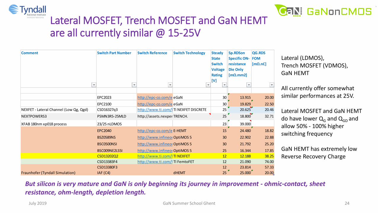
Lateral MOSFET, Trench MOSFET and GaN HEMT are all currently similar @ 15-25V
Comment Switch Part Number Switch Reference Switch Technology Steady
State
Switch
Voltage
Rating
[V]
V
r
e
v
_
I
r
Sp.RDSon
Specific ON-
resistance
Die Only
[mΩ.mm2]
QG.RDS
FOM
[mΩ.nC]
EPC2023 http://epc-co.com/epc/Portals/0/epc/documents/datasheets/EPC2023_preliminary.pdfeGaN 30 13.915 20.00
EPC2100 http://epc-co.com/epc/Portals/0/epc/documents/datasheets/EPC2100_preliminary.pdfeGaN 30 19.829 22.50
NEXFET - Lateral Channel (Low Qg, Qgd)
LDMOS => LOW QG and QGD
CSD16327q3 http://www.ti.com/lit/ds/symlink/csd16327q3.pdfTI NEXFET DISCRETE
Acq. Bottom Drain
25 20.625 20.46
NEXTPOWERS3
Need to describe this technology more
PSMN3R5-25MLD http://assets.nexperia.com/documents/data-sheet/PSMN3R5-25MLD.pdfTRENCH.
“SchottkyPlus”
25 18.800 32.71
XFAB 180nm xp018 process 23/25 nLDMOS 23 39.000
EPC2040 http://epc-co.com/epc/Portals/0/epc/documents/datasheets/EPC2040_datasheet.pdfE-HEMT 15 24.480 18.82
BSZ0589NS http://www.infineon.com/dgdl/Infineon-BSZ0589NS-DS-v02_00-EN.pdf?fileId=5546d46258fc0bc101598da704fa60e0OptiMOS 5 30 22.902 22.88
BSC0500NSI http://www.infineon.com/dgdl/Infineon-BSC0500NSI-DS-v02_00-EN.pdf?fileId=5546d4624eeb2bc7014efd4e65546362OptiMOS 5 30 21.792 25.20
BSC009NE2LS5I http://www.infineon.com/dgdl/Infineon-BSC009NE2LS5I-DS-v02_00-EN.pdf?fileId=5546d4624bcaebcf014c09a38586234eOptiMOS 5 25 16.344 17.85
CSD13202Q2 http://www.ti.com/lit/ds/symlink/csd13202q2.pdfTI NEXFET 12 12.188 38.25
CSD13383F4 http://www.ti.com/lit/ds/symlink/csd13383f4.pdfTI FemtoFET 12 21.090 74.00
CSD13380F3 12 23.814 57.33
Fraunhofer (Tyndall Simulation) IAF (C4) dHEMT 25 25.000 20.00
Lateral (LDMOS), Trench MOSFET (VDMOS),GaN HEMT
All currently offer somewhat similar performances at 25V.
Lateral MOSFET and GaN HEMT do have lower QG and QGD and allow 50% - 100% higher switching frequency
GaN HEMT has extremely low Reverse Recovery Charge
But silicon is very mature and GaN is only beginning its journey in improvement - ohmic-contact, sheet resistance, ohm-length, depletion length.
24July 2019 GaN Summer School Ghent

Evaluation of 15V EPC for 5V POL Application(versus 180nm CMOS)
25July 2019 GaN Summer School Ghent

EPC2040 (15V eHEMT) vs 180nm 5V CMOS (=RON)
EPC 5V 180nm CMOS
Both EPC2040 & 180nm 5V CMOS set for equal RON ~ 24mΩ.
W/L ratio of 80e-3/0.5e-6 for ne5
26July 2019 GaN Summer School Ghent

EPC2040 vs 180nm 5V CMOS (=RON)
Sweeping Load Current
(Ripple Current ~0.0622A)
-to effectively sweep IF for the body
diode or 3rd quadrant conduction
mechanism
27July 2019 GaN Summer School Ghent

EPC2040 vs 180nm 5V CMOS (=RON)
EPC
180nm 5V CMOS
15V eHEMT EPC2040
Comparable Coss – 15V GaN slightly better than 5V CMOS
No significant Body Diode Reverse Recovery Issue for 5V Converter with ordinary bulk CMOS
Simulations Eoin Walsh(MSc.Eng. Tyndall)
28July 2019 GaN Summer School Ghent
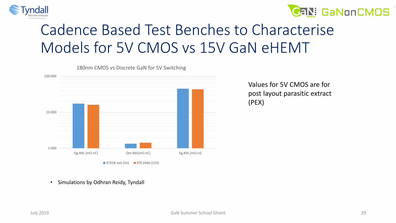
• Simulations by Odhran Reidy, Tyndall
Cadence Based Test Benches to Characterise Models for 5V CMOS vs 15V GaN eHEMT
1.000
10.000
100.000
Qg.Rds [mΩ.nC] Qm.Rds[mΩ.nC] Eg.Rds [mΩ.nJ]
180nm CMOS vs Discrete GaN for 5V Switching
XT018 ne5 (5V) EPC2040 (15V)
Values for 5V CMOS are for post layout parasitic extract (PEX)
29July 2019 GaN Summer School Ghent
30
POL/VR Demonstrators
July 2019 GaN Summer School Ghent

• POL to baseline with best COTS (EPC and Peregrine Driver)
• 3-L POL to further develop 4X reduction in Inductor and coupled-L
• Evaluate IAF 25V d-HEMT
• Evaluate IHP 25 MHz Controller/Driver Combo
• Prototype 10 MHz Resonant Converter
Open Loop POL PCB Level DEMONSTRATORS
31July 2019 GaN Summer School Ghent

• 1 MHz
• IAF Asymmetric Half Bridge d-HEMT
• Inductor will degrade efficiency by further 5%
• Require > ~88% to have a viable solution
• Note capacitive couplings between phases for monolithic
Monolithic Asymmetric Half Bridge
32July 2019 GaN Summer School Ghent

• 100V IAF switches with copper (125um thick) contacts and switch copper pattern design for compatibility with PCB embedding manufacturing process.
• Separate test board planned for design and build to cycle large embedded switch power dissipations and perform reliability trials
• Trial IBM Copper Pillar interconnect technology on discrete IAF switch, ahead of GaNonCMOS top level interconnect.
Stack Level Designs to be Evaluated
33July 2019 GaN Summer School Ghent
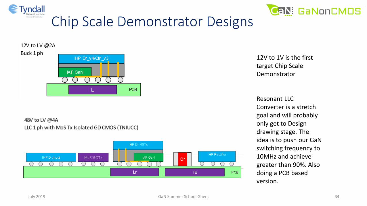
Chip Scale Demonstrator Designs
34
12V to 1V is the first target Chip Scale Demonstrator
Resonant LLC Converter is a stretch goal and will probably only get to Design drawing stage. The idea is to push our GaN switching frequency to 10MHz and achieve greater than 90%. Also doing a PCB based version.
July 2019 GaN Summer School Ghent

July 2019 GaN Summer School Ghent 35
PCB Demo 4 & Chip Level Stretch Demo 2
• High frequency GaN switch application requires integrated gate driver
• High side switches require isolated gate drive.
• Magnetic coupled power and signal creates the best possible solution• The alternative is capacitive. Capacitive coupled gate driver power creates common mode transient injection due
to high dV/dt on switching nodes (100-500V/ns).
• TNIUCC and IHP, in partnership, taped out, a 2-Chip chip-set to validate Magnetics–on-Silicon (MoS) gate driver isolation transformer – this can be the basis of a smart CMOS gate driver for GaN switches.
• TNIUCC taped out a 3rd IC to create a low voltage CMOS synchronous rectifier set for 4A output isolated or high frequency resonant point-of-load (POL) converter (Will suit 12, 24, 48V POL)
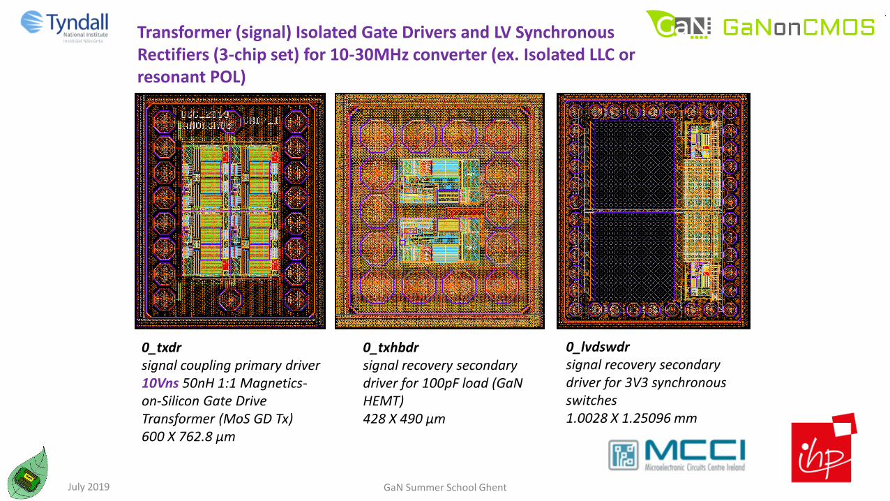
0_txdrsignal coupling primary driver10Vns 50nH 1:1 Magnetics-on-Silicon Gate Drive Transformer (MoS GD Tx)600 X 762.8 µm
0_txhbdrsignal recovery secondary driver for 100pF load (GaN HEMT)428 X 490 µm
0_lvdswdrsignal recovery secondary driver for 3V3 synchronous switches1.0028 X 1.25096 mm
Transformer (signal) Isolated Gate Drivers and LV Synchronous Rectifiers (3-chip set) for 10-30MHz converter (ex. Isolated LLC or resonant POL)
July 2019 GaN Summer School Ghent

37
A variety of 25V and 100V Switches and Monolithic Bridges are being developed by Fraunhofer IAF
Also creating some which will be appropriate for Multi-Level
July 2019 GaN Summer School Ghent

GaN/ AlGaN HEMT - Final Interconnect Stages of
Fabrication
Interconnection metal Ti/Pt/Au
Source shield
Ohmic contacts Ti/Al/Ni/Au
Device isolation by implantation
NiAu Gate
SiN passivation stages
Ti/Pt/Au Source Shield & Interconnect
38July 2019 GaN Summer School Ghent

Final Passivation Opening and Copper Plating
5 um Copper Plating
39July 2019 GaN Summer School Ghent

AlGaN/GaN High Electron
Mobility Transistor
Source
Drain
Gate
S D
G
AlGaN
GaN
SiNX
2DEG
Si substrate
40July 2019 GaN Summer School Ghent
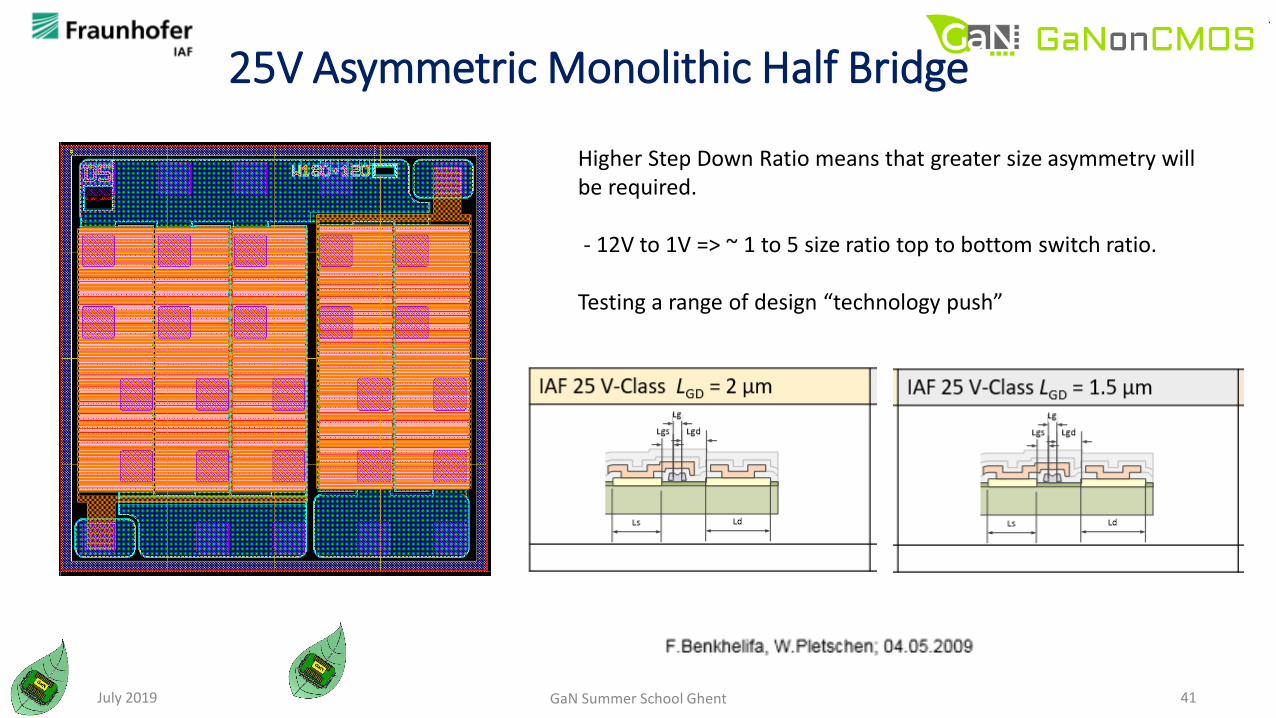
25V Asymmetric Monolithic Half Bridge
Higher Step Down Ratio means that greater size asymmetry will be required.
- 12V to 1V => ~ 1 to 5 size ratio top to bottom switch ratio.
Testing a range of design “technology push”
41July 2019 GaN Summer School Ghent

42
PCB Embedding Technology
July 2019 GaN Summer School Ghent

Drain
Source
Gate
Vertical –Power Transistor (Si, SiC)
Lateral –GaN-on-Si Transistor
Gate
GaN
Si-Substrate
Source DrainAlGaN
2DEG
July 2019 43
Source
Drain
Gate
Multi-bond wireswith small diameters?<100 µm
GaN
Si-Substrate
GateSourc
eDrain
AlGaN
GaN Summer School Ghent

SiGaN
Cu
Solder
Bond Wire
Active Area
Leadframe
PCB Embedding
SiGaN
PC
B
Thermal Pad
Elect. Top Pads
Elect. Bottom Pads
Active AreaThrough -Via
Mirco-Via
Mirco-Via
Micro
vs
PCB-Embedding for GaN-on-Si Power Devices and Ics – CIPS 2018, R.Reiner et al.
- shows interconnect inductances LD and LS ~ 1nH (by comparison 1nH/mm for bond wire solutions)
- shows thermal performance < 1K/W achievable with large diameter micro-vias
GaN-on-CMOS working to improve with heavy Cu devices contacts and patterns to match PCB manufacturing technology.
44July 2019 GaN Summer School Ghent

45
All Copper – No brittle inter-metallics
Low Processing Temperature
July 2019 GaN Summer School Ghent

CMOS Gate Driver Development
July 2019 46GaN Summer School Ghent

Design of Driver IC Version 2Relaxed design due to new GaN switches
• Voff ≈ -3.5 V
New level shifter circuit
• Galvanically isolated up to 25 V
• Adaptable to some hundreds of volts
Optimized switching transitions
• Adjusted to minimum losses
• 2 A peak output currents
Working from 1 to 30 MHz
GaNonCMOS
HSP
SW
PWMHSHSN
VDD
VBSGND
output stageNon-overlapping
switch
LSP
VSS
PWMLSLSN
VDD
VNNGND
output stageNon-overlapping
switch
GaN Summer School Ghent 47

Galvanically Isolated Driver IC
Building blocks• Half-bridge driver
• IHP and Peregrine Driver driving 1nF.
• 66.7% rise time for 3V3 input pulse:
• IHP – 1.798nS,
• PD – 2.79nS
• High side branch with bootstrapped supply
• Isolated domains
• 200 µm octagonal pads as of v1
Taped out chip• Taped out: Aug 29 2018
• Wafer out : beginning of 2019
• Area: 2.1 x 2.1 mm², pad limited
GaN Summer School Ghent 48

Passive ComponentsInductor(s) and Capacitors
49July 2019 GaN Summer School Ghent

Silicon Capacitors for High Density Solution
ESL provides necessary ripple advantage
High SRF – 100’s MHz
50
Murata-IPDiA
July 2019 GaN Summer School Ghent

• The POL inductor is by far and away the largest component when in low profile format 5-15 X semiconductor size at 1-2MHz
• => Change topology to Multi-Level (3-L for 4X reduced L value) and push switching frequency
• Inverse Phase coupling arrangements cancel DC field and may give steady state ripple (L-value) advantage. Multi-Level helps by extending Duty (optimum coupling values) for Low Voltage POL
• Searching and Qualifying COTs materials for Embedded PCB Applications – Co-operation AT&S
• Tyndall is developing new multi-laminate thin film (plated and sputtered) PCB embeddable magnetic cores
• Planar Embedded with 300-500 um Cores are most appropriate for 1-10MHz low profile GaNonCMOS POL. They can have low DCR with AT&S thicker Cu.
GaN-on-CMOS Magnetic Materials & Device Design
51July 2019 GaN Summer School Ghent

Tyndall designed and fabricated world’s highest Q MoS inductor at 30MHz for on-chip power conversion< 45um height.
White-hot regions are CMOS Gate Drivers and GaN switches at 30MHz. 50 nH MoS Inductor does not appear on heat map.
Low DCR
High QAC
Magnetic Component Technology based on Peak Q Frequency
July 2019 GaN Summer School Ghent

Magnetics-on-Silicon (MoS)thin film Gate Driver Isolation Transformer
Is being designed for GaN-on-CMOS Smart Driver Application
Thin film solenoidal and Racetrack Constructions - 50 µm Profile
<<10 V.ns
~ 1mm2
Based on highest Q thin film MoS by Tyndall as reported at IEEE PwrSoC 2019
MoS step improvement in mid. 2000’s
Donald S. Gardner et al. (INTEL)
Review of On-Chip Inductor Structures With
Magnetic Films
IEEE TRANSACTIONS ON MAGNETICS,
VOL. 45, NO. 10, OCTOBER 2009
53July 2019 GaN Summer School Ghent

GaNonCMOS Embedded Magnetics will extend this type of analysis to Low Profile Magnetics (PCB Embedded)
Wound Magnetic Device Performance Factor“Measurements and Performance Factor Comparisonsof Magnetic Materials at High Frequency”Alex J. Hanson, Student Member, IEEE, Julia A. Belk, Student Member, IEEE,Seungbum Lim, Student Member, IEEE, Charles R. Sullivan, Fellow, IEEE, and David J. Perreault, Fellow, IEEE
We will create a similar Embedded Device Performance Factor for material in planar toroid format in PCB windings
SOA High Frequency Ferrite
54July 2019 GaN Summer School Ghent
Wafer-Wafer Bonding Trials
55July 2019 GaN Summer School Ghent
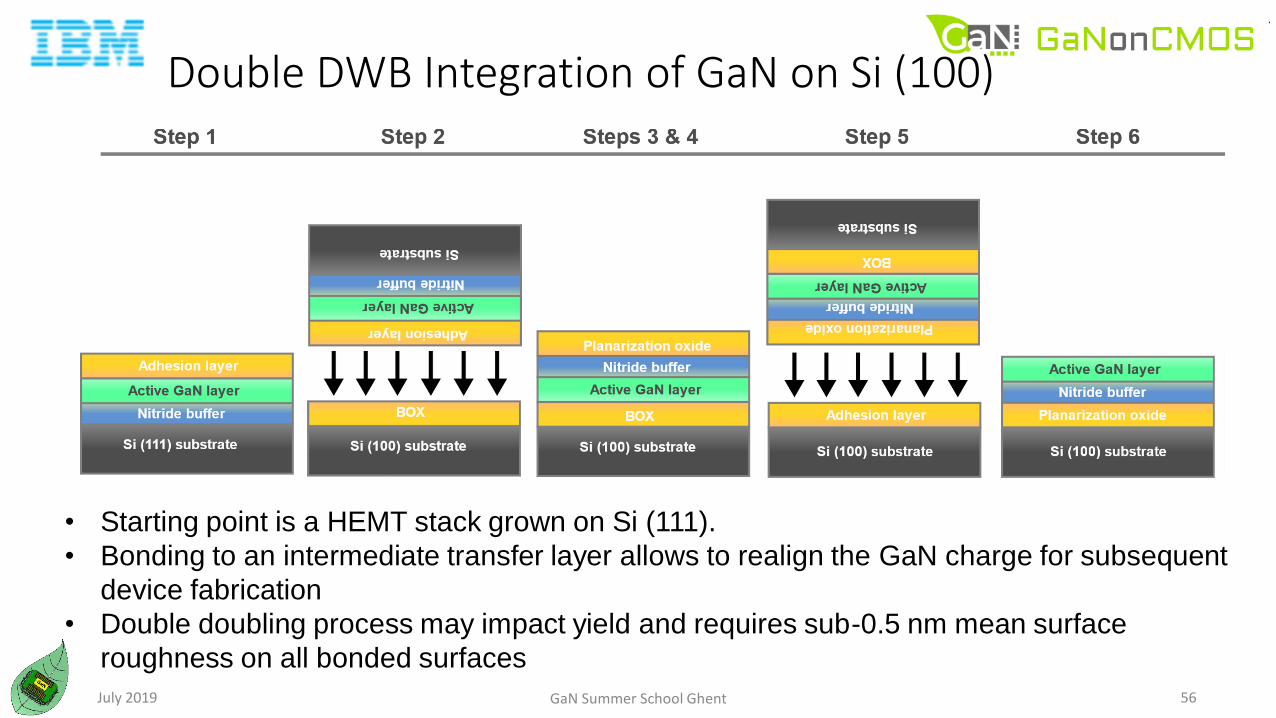
Double DWB Integration of GaN on Si (100)
• Starting point is a HEMT stack grown on Si (111).
• Bonding to an intermediate transfer layer allows to realign the GaN charge for subsequent
device fabrication
• Double doubling process may impact yield and requires sub-0.5 nm mean surface
roughness on all bonded surfaces
56July 2019 GaN Summer School Ghent

57
2XDWB – GaN on Si (100)
• 2XDWB after Si removal, with bonding oxides remaining
• Bowing results in delamination in the center area.
• Can be optimized by strain engineering
SiN capping layer exposed,
~8 pieces of 1.5cm chips
July 2019 GaN Summer School Ghent

58
Crystal Quality of Bonded GaN Layer
SiO2
~ 8 nmSiN
~ 18 nm AlGaN
GaN
• TEM analysis of double-bonded
layer
• Active device layers crystal
quality not affected by bonding
process
July 2019 GaN Summer School Ghent

3D Integrated Power Switch and CMOS Driver
• Double wafer bonding process allows to integrated GaN switches with CMOS drivers
monolithically
• Alignment between the two device layers is achieved by implementing markers on both
layers, and using a retractable double-side camera - ~2 µm accuracy
• Circuit co-design allows straightforward interconnect formation
• Planarisation Process Fraunhofer ENAS
59July 2019 GaN Summer School Ghent

1st Engineering Prototype Chip Scale GaN-on-CMOS Options
Ideal is probably for GaN Switch Design to be Smaller than CMOS design
GaN Device can be flip-chipped down onto Application Substrate with highest current contacts and highest thermal conduction path.
60July 2019 GaN Summer School Ghent

61
What are the Optimum Ratios of GaN to CMOS?
July 2019 GaN Summer School Ghent
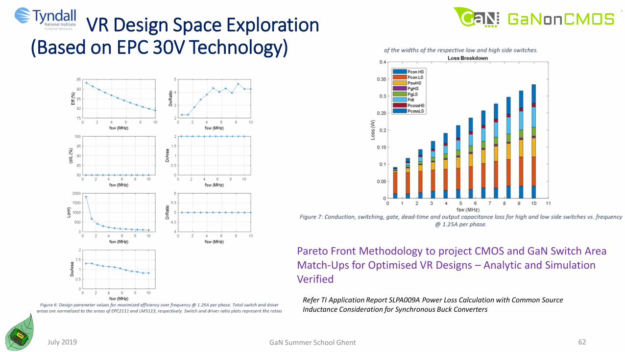
VR Design Space Exploration (Based on EPC 30V Technology)
Pareto Front Methodology to project CMOS and GaN Switch Area Match-Ups for Optimised VR Designs – Analytic and Simulation Verified
Refer TI Application Report SLPA009A Power Loss Calculation with Common Source Inductance Consideration for Synchronous Buck Converters
62July 2019 GaN Summer School Ghent

Optimised Semiconductor Designs for 90+% efficient 12-1V 2MHz Buck (4mm2) and 10MHz LLC (4.82mm2)
Buck POL: Silicon Capacitors and Chip Inductor Passives Require 9mm2
Semiconductor Area Ratios for Optimised Design 12 to 1V (2.5A) 10 MHz LLC
CMOS SRs3V3 Sec.RectifiersAreamm2
GaNSwitchesAreamm2
CMOSGaN DriverIHP SG13S130 nm 3V3mm2
CTRLCMOS(Per Phase)Areamm2
Semiconductor Area Ratios for Optimised Design12 to 1V (1.25A) 2MHz Buck VR
GaNSwitches(25V)Areamm2
CMOSDriversArea130 nm 3V3mm2
CMOSCTRL(1-φ)Areamm2
• High fsw ZVS (Soft Switched, Resonant) Applications could use GaN-on-CMOS for Smart Switches – nice area balance down to 25V VBR.
• Isolated Stage Capability – CM noise and EMI advantage
• Large sink current capability on drivers for dVSN/dt requires large drivers in efficiency optimised design – area imbalance at 25V VBR => Higher Vin & higher Duty applications => RDSon
scales with VBR2 but RDS.QG FOM(VDS) => Gate driver strength
can decrease strongly as VSW increases. Similarly for Qoss loss.
• Low Duty Cycle (low Vo) POL application challenged for SR FET.
63July 2019 GaN Summer School Ghent

GaN with Integrated Driver• CMOS Drive is better
• Specific On Resistance for Low Voltage CMOS drivers are much lower than 25V GaN
• 3V3 – 5V CMOS• Sp.RON = 2.5 – 6
mΩ.mm2
• Smart Driver Features require CMOS
• Isolated GD (Pulse) Signal recovery
• Adaptive Delay Management
• 3rd Quadrant Drive• Protection
Features64July 2019 GaN Summer School Ghent

Monolithic Bridge Considerations- floating bulk?
S. Moench, C. Salcines, R. Li, Y. Li and I. Kallfass, "Substrate potential of high-voltage GaN-on-Si HEMTs
and half-bridges: Static and dynamic four-terminal characterization and modeling," 2017 IEEE 18th Workshop
on Control and Modeling for Power Electronics (COMPEL), Stanford, CA, 2017, pp. 1-8.
65
Current Collapse
QGSwitching Speed COSS
July 2019 GaN Summer School Ghent

• Silicon Switch Stacks for 600V Applications• Multi Level Topology and lower Voltage LDMOS/ VDMOS Switch Stacks per Cell
• Fine Geometry CMOS Switch Stacks and ML for 12V Applications?• Isolated switch stacks have large Specific Ron but can have very low switching FOM• Economics will have a say!
Technical Competition for GaN
66July 2019 GaN Summer School Ghent
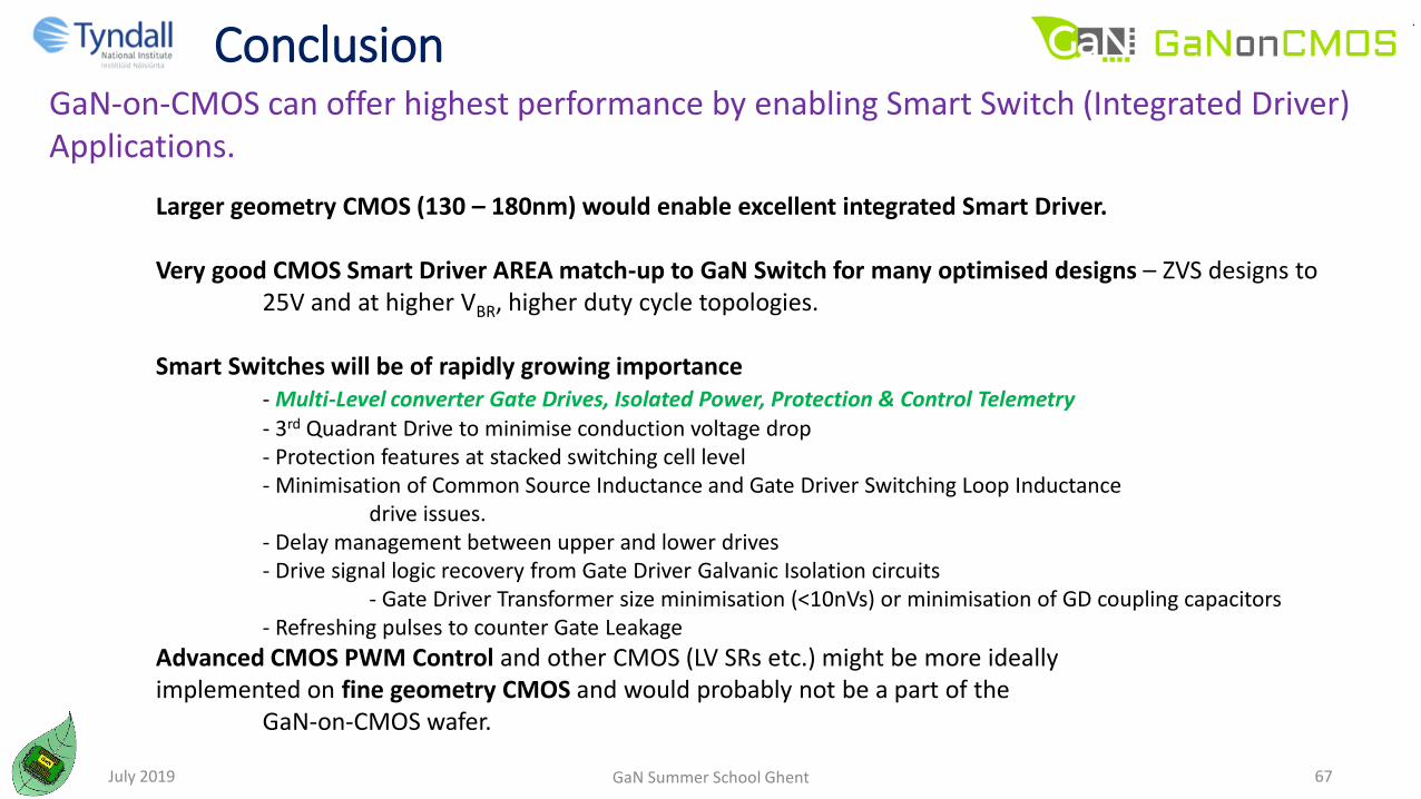
ConclusionGaN-on-CMOS can offer highest performance by enabling Smart Switch (Integrated Driver) Applications.
Larger geometry CMOS (130 – 180nm) would enable excellent integrated Smart Driver.
Very good CMOS Smart Driver AREA match-up to GaN Switch for many optimised designs – ZVS designs to 25V and at higher VBR, higher duty cycle topologies.
Smart Switches will be of rapidly growing importance- Multi-Level converter Gate Drives, Isolated Power, Protection & Control Telemetry- 3rd Quadrant Drive to minimise conduction voltage drop- Protection features at stacked switching cell level- Minimisation of Common Source Inductance and Gate Driver Switching Loop Inductance
drive issues.- Delay management between upper and lower drives- Drive signal logic recovery from Gate Driver Galvanic Isolation circuits
- Gate Driver Transformer size minimisation (<10nVs) or minimisation of GD coupling capacitors- Refreshing pulses to counter Gate Leakage
Advanced CMOS PWM Control and other CMOS (LV SRs etc.) might be more ideally implemented on fine geometry CMOS and would probably not be a part of the
GaN-on-CMOS wafer.
67July 2019 GaN Summer School Ghent

• Smart Switches and Smart Bridges for Automotive, Energy (Distributed Generation, Prosumer), Aerospace, Data-Centre Power and Servers, Industrial Drives, … everywhere from today’s > 50VBRswitches is technically hugely attractive.
• Multi-Level Topologies are very important (solution density) => 100-200V GaN & Smart Switches
• Heterogeneous Integrated Monolithic Bridge Converter solutions for Multi-Level/Multi-Phase for Multi-Node HPC –more attractive for 48V
• 12V POL challenged to get to higher switching frequency• LV switch technology needs to improve 3X with regard to switching FOMs• Magnetising Inductance value requires 10X in switching frequency• Resonant requires large area low silicion voltage rectifiers
• Other areas such as 5G Envelope Trackers (ET) in Cell Site RF Transmitters• Massive MIMO will require large array of GaN ET with CMOS drives• ET bandwidth must generally extend to several hundred MHz• Some solutions may usefully use GaN switches at 25-50V type voltage levels or possibly GaN/low voltage CMOS Cascodes.
GaN-on-CMOS Applications
68July 2019 GaN Summer School Ghent

– Project partners who supplied material IBM, RECOM, AT&S, IAF, IHP
- All Project Partners
- KU Leuven Project Co-ordinator and Project Leader
Acknowledgements
69July 2019 GaN Summer School Ghent

Back-Up
July 2019 70GaN Summer School Ghent

100 V-Layout-Design for AT&S - ECP®-PCB-Embedding
71July 2019 GaN Summer School Ghent


