
EE 172 Final Project
Evanescent Mode Filter
Svetoslav (Sam) Mandev
May 30, 2011

Introduction
There are various types of microwave filters being used in the RF industry, each with its own
advantages and shortcomings. Some examples include coaxial, stripline, microstrip, cavity, and
waveguide filters. Among them, waveguide filters are known to have very low loss and high Q
factors, while their application is mostly limited by their relatively large size compared to
standard transmission lines. One way to implement waveguide filters with smaller dimensions
is to use them in evanescent mode, or below cutoff frequency. For example, if we wish to
implement a 2 GHz circular waveguide filter, we could either use a 4-inch circular waveguide
(fc=1.73GHz) in a propagating mode, or we could use a 3-inch circular guide (fc=2.31GHz) in
evanescent mode, for a 25% reduction in diameter. Waveguides operating in evanescent mode
are well-suited to operate as filters, due to their high attenuation in the bandstop range.
Theory
1. Lumped element model of evanescent mode filter
By modeling the waveguide with lumped elements, the filter can be designed using
standard design techniques. A waveguide in evanescent mode can be represented by
equivalent T or π-sections of lumped inductances [Fig. 1 (b) and (c)] according to [1],[2]. For
moderate bandwidths ( <20% ), Craven and Mok [2] show that the quantity 2
l* is virtually
independent of frequency, and the evanescent waveguide can be approximated as in Fig. 1 (d)
using inductively coupled LC resonators.

Here, 12
2
0
0
f
f
c
f c is the propagation constant, or in this case – the
attenuation of the waveguide below cutoff.

Furthermore, the bandpass ladder network [Fig. 2 (b)] can be derived from the low-pass
prototypes [Fig. 2 (a)], using basic filter transformations as shown in Table 8.6 in Pozar’s text
[4].

The equivalent lumped reactance and susceptance values can be obtained as follows:
- a shunt capacitor, kC , in the low-pass prototype is transformed to a shunt LC circuit
with element values,
k
kCw
L0
'
, 0
'w
CC k
k
, where 0
12
w
ww is the fractional BW of the bandpass , and
kk gC
- series inductors,
kL , of the low-pass prototype are converted to parallel LC circuits
having element values,
0
'w
LL k
k
,
k
kLw
C
0
1' , where kk gL
G-values for Butterworth (Maximally flat) and Chebyshev (Equal-ripple) low-pass filters, are
tabulated in various texts including Pozar’s and Collin’s *4+,*5+. This forms the basis for the
lumped-element model of the Craven-type evanescent mode filters. Using the filter
transformations, the lumped model can be accurately simulated, and filter response obtained,
using proper reactance and susceptance values. I have presented a Microwave Office
simulation and filter response for my particular implementation, further in the paper.
2. Designing and building the waveguide filter
The cited papers by Craven and Mok [2], and Howard and Lin [3], explain in detail the
relationship between the lumped element values and the dimensions of the waveguide filter.
They present different methods for implementing resonating obstacles into the waveguide,
various coupling types, Q-factor calculation, and other interesting considerations. In this
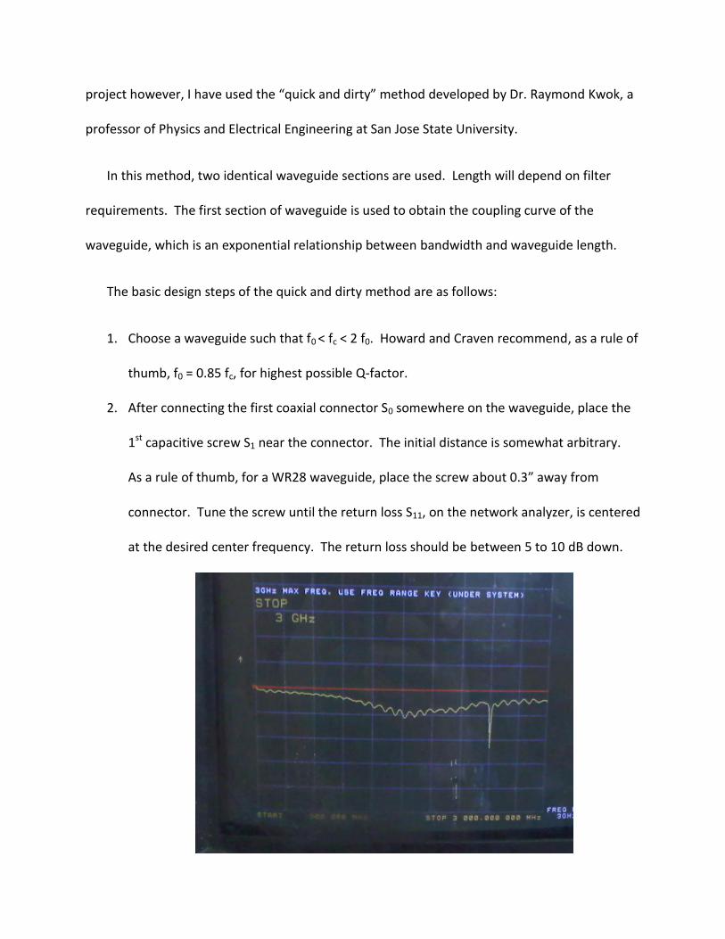
project however, I have used the “quick and dirty” method developed by Dr. Raymond Kwok, a
professor of Physics and Electrical Engineering at San Jose State University.
In this method, two identical waveguide sections are used. Length will depend on filter
requirements. The first section of waveguide is used to obtain the coupling curve of the
waveguide, which is an exponential relationship between bandwidth and waveguide length.
The basic design steps of the quick and dirty method are as follows:
1. Choose a waveguide such that f0 < fc < 2 f0. Howard and Craven recommend, as a rule of
thumb, f0 = 0.85 fc, for highest possible Q-factor.
2. After connecting the first coaxial connector S0 somewhere on the waveguide, place the
1st capacitive screw S1 near the connector. The initial distance is somewhat arbitrary.
As a rule of thumb, for a WR28 waveguide, place the screw about 0.3” away from
connector. Tune the screw until the return loss S11, on the network analyzer, is centered
at the desired center frequency. The return loss should be between 5 to 10 dB down.

3. Connect screw S2 next to S1 (arbitrary distance) and tune until two peaks are visible on
the screen.

Keep tuning until both peaks are at about equal distance from f0, placed symmetrically
around the f0. Here, )(2
1210 fff . At this point measure and record ∆X and ∆f.
4. Move S2 and repeat measurement, until enough data is obtained in order to plot
coupling curve. The farther S2 is from S1, the smaller the peaks (dibs) will be, since the
signal is being attenuated fast.
5. Plot coupling curve “ln(∆f) vs. ∆X” on semi-log paper. Plot should be a straight or near
straight line. Extract slope and y-intercept of plot.

6. Once the required filter specs are determined (BW, number of sections, ripple dB), the
new ∆X distances between the tuning screws can be calculated from the coupling curve,
as follows:
a. Using the published g-values for the specific dB ripple and BW, calculate the new
∆f’s from the equation 1
1,
ii
iigg
BWf
b. From the calculated ∆f’s, extract the distances between the resonators from the
coupling curve.
7. Design the distances between the connectors and the first screw. The process is
somewhat arbitrary, and experimentation may be necessary based on desired coupling,
but here are some suggestions:
a. Guideline: 0.15” is sufficient for WR28 waveguide (Dr. Kwok’s example)
b. Craven and Mok [2] suggest the following approximation: 1)coth( 0 l for up
to four significant figures.
c. Dishal Method – design the connector-to-screw length based on desired external
Q-factor. The method entails making several test models with different coupling
positions ‘h’, tuning S1 screw to the same frequency, and then plotting
Q(external). vs ‘h’ [8],[9]. Then design based on plotted curve. Here, f
fQext
0
Any of the above suggestions are good starting points, but further measurements
may be needed for the connector couplings. Also, the length of the connector pin is
an important consideration.

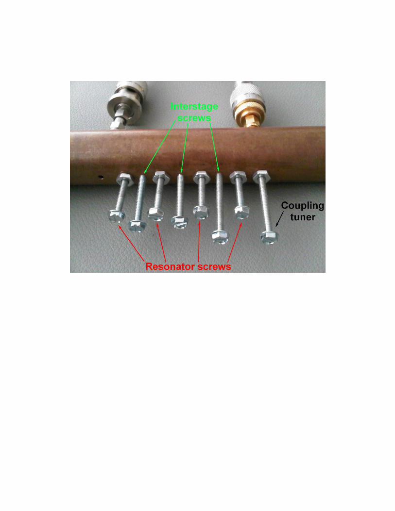
8. Build and tune filter. Fine tune using interstage screws, roughly midway between the
resonating screws. Tune the coupling pins if needed.
Design Example
My particular design is for a 4-section, 0.1dB Chebyshev Equal-ripple filter, operating at
center frequency 4.2GHz with 300MHz bandwidth.
1. MWO Simulation
The model has four LC resonators, equivalent to the resonating screws on the waveguide.
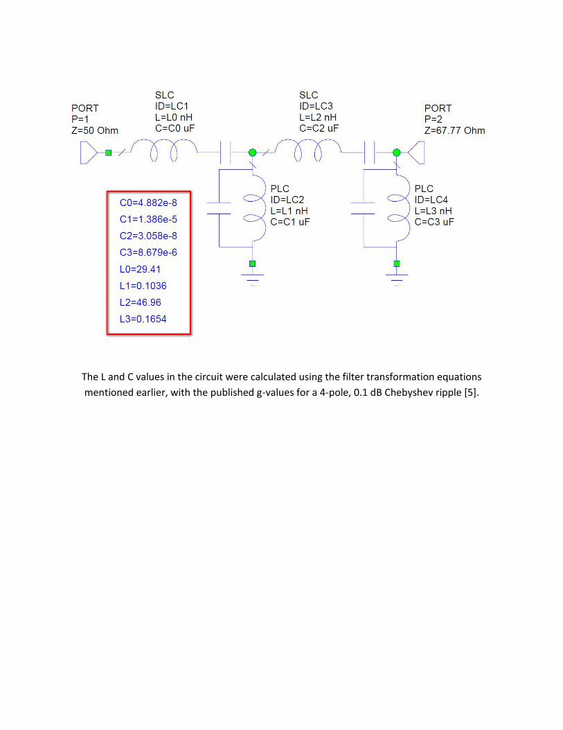
The L and C values in the circuit were calculated using the filter transformation equations
mentioned earlier, with the published g-values for a 4-pole, 0.1 dB Chebyshev ripple [5].

BW = 300 MHz, RL ≈ 16dB


2. Waveguide measurements, coupling curve
1-inch diameter copper pipe, GHza
cf
nmc 922.62
841.1
Measurements
∆X (inch) ∆f (GHz) ∆f (Hz) ln(∆f)
0.759 0.24 240000000 19.296149
1.09 0.08 80000000 18.197537
1.33 0.05106 51060000 17.748512
1.658 0.03014 30140000 17.221364
2.005 0.0089 8900000 16.001562
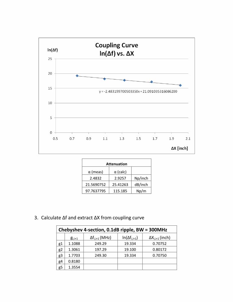
Attenuation
α (meas) α (calc)
2.4832 2.9257 Np/inch
21.5690752 25.41263 dB/inch
97.7637795 115.185 Np/m
3. Calculate ∆f and extract ∆X from coupling curve
Chebyshev 4-section, 0.1dB ripple, BW = 300MHz
gi,i+1 ∆fi,i+1 (MHz) ln(∆fi,i+1) ∆Xi,i+1 (inch)
g1 1.1088 249.29 19.334 0.70752
g2 1.3061 197.29 19.100 0.80172
g3 1.7703 249.30 19.334 0.70750
g4 0.8180
g5 1.3554

4. Building the filter
Connector pin length ≈ 5/6 of diameter (SMA pin extended with a
3mm wire for better coupling)
Did not change the distance between S0 and S1 (≈0.5”)
Tuning screws / nuts : #6-32 (tapped)
Connectors: SMA panel mounts + SMA to N-type adapters
SMA connectors bolted with #2-56 screws (tapped and bolted)


5. Tuning the filter – for 0.1 dB ripple, need to achieve ≈16dB Return Loss


6. Conclusion, observations, and suggestions
~15dB of Return Loss (S22) achieved, BW = 200MHz
Only one of the couplers could be tuned for a small difference. That means that
the connectors may have been over or under-coupled. For better result, need to
design coupling positions as described in design steps - Craven/Howard
approximation *2+,*3+ or Dishal’s method *8+,*9+.
When tuning the first screw by itself, it produced a low and wide peak, which
also indicates that poor coupling, as mentioned above.
For easy calculation of external and unloaded Q factors, refer to [7] by Dr. Ray
Kwok

References
[1] G. Craven, "Waveguide Below Cutoff: A New Type of Microwave Integrated Circuit,"
Microwave Journal, Vol. 13, August 1970, p. 51.
[2] G. Craven and C. Mok, "The Design of Evanescent Waveguide Bandpass Filter for a
Prescribed Insertion Loss Characteristics," IEEE Trans. MTT, Vol. MTT-19, March 1971.
[3] Howard, John and Wenny C. Lin. "Evanescent mode filter: design and implementation."
Microwave Journa/32.10 (1989): 121+. Academic OneFile. Web. 18 May 2011.
[4] D. M. Pozar, Microwave Engineering, 3rd ed., John Wiley & Sons, New York, 1998.
[5] R. E. Collin, Foundation for Microwave Engineering, 2nd ed., McGraw-Hill, New York,
1992.
[6] Kwok, Raymond S. “Notes on Evanescent Bandpass Filter”. 1991
[7] Kwok, Raymond S. and Liang, Ji-Fuh “Characterization of High-Q Resonators for
Microwave-Filter Applications”. 1999
[8] M. Dishal, “Alignment and Adjustment of synchronously tuned multiple-resonant -circuit
filters” Proc I.R.E. vol 39 November 1951
[9] M. Dishal, “A Simple Design Procedure for Small Percentage Bandwidth Round Rod
Interdigital Filters” MTT Vol13 Sept 1965 p 696


