
P a g e | 1
ELECTRONIC DEVICES AND CIRCUITS
LEARNING OBJECTIVES:
Concept of oscillator.
Study of barkhausen criterion.
About different types of oscillators.
CHAPTER-4(SINOSOIDAL OSCILLATORS)
4.1 POSITIVE FEEDBACK
Feedback is the process of picking up a part of the output signal of an amplifier and feeding it at
the input.
The voltage so fed back to the input is called the feedback voltage.
Positive Feedback: Feedback is called positive (or regenerative) feedback, when the feedback
signal is in phase with the input and adds to the input signal. This results in increase of the gain of
the amplifier. But it has the disadvantage of increased instability of gain, increased distortion and
noise. Hence, positive feedback is rarely used in amplifiers. However positive feedback is used in
oscillators.
4.2 USE OF POSITIVE FEEDBACK
Positive feedback is used in oscillators to keep them running or oscillating. An oscillator
is basically an amplifier which has a feedback path from the output back to the input.
This permits a portion of the output signal to get back to the input to "keep things
going" in stage - to keep things oscillating. The feedback must be positive so that it
will "contribute" to the stage being able to keep oscillating. If the feedback was
negative, it would serve to damp the oscillation and to "kill" the oscillator
4.3 OSCILLATORS
The oscillators are electronic circuits makes a respective electronic signal generally the
sine wave and the square wave. It is very important in other types of the electronic
equipment such as quartz which used as a quartz oscillator. The amplitude
modulation radio transmitters use the oscillation to generate the carrier waveform.
The AM radio receiver uses the special oscillator it is called as a resonator to tune a
station.
4.3.1 Parts of an Oscillator
Most oscillators consist of three basic parts:
4.3.1.1. An amplifier. This will usually be a voltage amplifier and may be biased in class A, B
or C.

P a g e | 2
4.3.1.2. A wave shaping network. This consists of passive components such as filter circuits
that are responsible for the shape and frequency of the wave produced.
4.3.1.3. A POSITIVE feedback path. Part of the output signal is fed back to the amplifier input
in such a way that the feed back signal is regenerated, re-amplified and fed back again to
maintain a constant output signal.
Commonly an oscillator is constructed from an amplifier that has part of its output signal fed
back to its input. This is done in such a way as to keep the amplifier producing a signal without
the need for any external signal input as shown in Fig. 1.1.1. It can also be thought of as a way of
converting a DC supply into an AC signal.
4.3.2 Positive feedback.
The feedback in the amplifier section of an oscillator must be POSITIVE FEEDBACK. This is
the condition where a fraction of the amplifier's output signal is fed back to be in phase with the
input, and by adding together the feedback and input signals, the amplitude of the input signal is
increased. For example, a common emitter amplifier creates a phase change of 180° between its
input and output, the positive feedback loop must therefore also produce a 180° phase change in
the signal fed back from output to input for positive feedback to occur.
The result of a small amount of positive feedback in amplifiers is higher gain, though at the cost
of increased noise and distortion. If the amount of positive feedback is large enough however,
the result is oscillation, where the amplifier circuit produces its own signal.
4.3.3 Using Positive Feedback.
When an amplifier is operated without feedback it is operating in "open loop" mode. With
feedback (either positive or negative) it is in "closed loop" mode. In ordinary amplifiers negative
feedback is used to provide advantages in bandwidth, distortion and noise generation, and in
these circuits the closed loop gain of the amplifier is much less than the open loop gain.
However when positive feedback is used in an amplifier system the closed loop gain (with
feedback) will be greater than the open loop gain, the amplifier gain is now increased by the
feedback. Additional effects of positive feedback are reduced bandwidth, (but this does not
matter in an oscillator producing a sine wave having a single freqency), and increased distortion.
However even quite severe distortion in the amplifier is allowed in some sine wave oscillator
designs, where it does not affect the shape of the output wave.
In oscillators using positive feedback it is important that amplitude of the oscillator output
remains stable. Therefore the closed loop gain must be 1 (unity). In other words, the gain within
the loop (provided by the amplifier) should exactly match the losses (caused by the feedback

P a g e | 3
circuit) within the loop. In this way there will be no increase or decrease in the amplitude of the
output signal, as illustrated in Fig. 1.1.2.
4.4.4 The conditions for oscillation.
Positive feedback must occur at a frequency where the voltage gain of the amplifier is equal to
the losses (attenuation) occurring in the feedback path. For example if 1/30th of the output signal
is fed back to be in phase with the input at a particular frequency, and the gain of the amplifier
(without feedback) is 30 times or more, oscillation will take place.
The oscillations should take place at one particular frequency.
The amplitude of the oscillations should be constant.
There are many different oscillator designs in use, each design achieving the above criteria in
different ways. Some designs are particularly suited to producing certain wave shapes, or work
best within a certain band of frequencies. Whatever design is used however, the way of
achieving a signal of constant frequency and constant amplitude is by using one or more of three
basic methods
.
Method 1
Make sure that positive feedback occurs only at one frequency, the required frequency of
oscillation. This may be achieved by ensuring that only signals of the required frequency are fed
back, or by ensuring the feedback signal is in the correct phase at only one frequency.
Method 2
Make sure that sufficient amplification for oscillation can take place only at the required
frequency, by using an amplifier that has an extremely narrow bandwidth, extending to the
frequency of oscillation only.
Method 3
Use amplifiers in "switch mode" to switch the output between two set voltage levels, together
with some form of time delay to control the time at which the amplifiers switch on or off, thus
controlling the periodic time of the signal produced.

P a g e | 4
Fig. 1.1.2 The Need For Amplitude Stability
Methods 1 and 2 are used extensively in sine wave oscillators, while method 3 is useful in square
wave generators, sometimes called aperiodic (untuned) oscillators. Oscillators using method 3
often use more than one amplifier and timing circuit, and so are called multivibrators (more than
one oscillator).
4.5 TYPES OF OSCILLATORS
There are two types of electronic oscillator’s they are linear and nonlinear oscillators. The linear
oscillators give the sinusoidal input. The linear oscillators consist a mass m and its force in the
linear in equilibrium. By applying the hook’s low the spring creates the force that i9s in linear for
small displacements.
The different types of oscillators are mentioned below and some of them are explained.
Crystal Oscillator
Hartley oscillator
RC Phase Shift Oscillator
Colpitts Oscillators
Phase Shift Oscillator
Wine Bridge Oscillator
4.6 LC OSCILLATORS.
LC oscillator is a type of oscillator where a LC (inductor-capacitor) tank circuit is used for giving
the required positive feedback for sustaining the oscillations. The LC tank circuit is also termed as
LC resonant circuit or LC tuned circuit. According to the Barkhausen criterion for sustained
oscillations, a circuit will sustain stable oscillations only for frequencies at which the loop gain of
the system is equal to or greater than 1 and the phase shift between input and output is 0 or an
integral multiple of  2π. LC oscillators can realized using BJT, FET, MOSFET, opamp etc.

P a g e | 5
Typical applications of LC oscillators include RF signal generators, frequency mixers, tuners, sine
wave generators, RF modulators etc. Before going into the LC oscillators in detail let’s have a look
at the LC tank circuit.
LC tank circuit.
Though the original tank circuit means a capacitor and
inductor connected in parallel, the switch and a voltage source are included in the circuit for the
ease of explanation. Initially the switch S is assumed to be in position 1. The cacpacitor will be
charged to a voltage V which is the voltage source. Assume the switch is moved to position 2 as
shown in the figure below.
The capacitor C will start discharging through inductor
L. The voltage across capacitor will start to decrease and the current through the inductor starts
increasing. The increasing current creates an electromagnetic field around the coil and when the
capacitor is fully discharged the electrostatic energy stored in the capacitor will be fully transferred
into the coil as electro-magnetic field. With no more energy in the capacitor to sustain the current
through the coil, the field around the coil starts to fall and the current through the coil tends to
decrease. Due to electromagnetic induction the inductor will generate a back emf equal to L(di/dt)
in order oppose the change in current. This back emf will start to charge the capacitor again.
When the capacitor is fully charged , the energy once stored in the inductor as elecro-magnetic
field will be moved  to the capacitor as electrostatic field. Then the capacitor starts discharging
again and the cycle is repeated. This cyclic transfer of of energy between the capacitor and inductor
is the reason behind the production of oscillations in the tank circuit.
If  an  ideal capacitor and inductor are used, these oscillation will sustain until the end of time.
But in  practical case  the inductor will have some ohmic resistance and the capacitor will have
some amount of leakage. These imperfections will waste some amount of energy in between the
cycles  resulting in the loss of amplitude step by step and eventually the oscillations will die out.
This gradual decay in amplitude which tends to the death of an oscillation is called damping. The

P a g e | 6
oscillations produced in a damped  LC tank circuit  will look like what shown in the figure
below.
In a practical LC oscillator, in addition to the Barkahusen criterion there must be some means to
compensate for the energy lost in the tank circuit. Application of active elements like BJT, FET,
opamp etc in the LC oscillator  is a way for meeting all these requirements. The active element in
an LC oscillator circuit has three essential jobs.
To give necessary gain.
Help in attaining the required positive feedback conditions.
Compensate the energy lost in the tank circuit.
4.6.1. LC oscillators and types.
4.6.1.1. Tuned collector oscillator.
Tuned collector oscillator can be said to be the basic type of LC oscillators. Here a transformer and
a capacitor connected in parallel across the collector circuit of the oscillator. Primary of the
transformer and the capacitor forms the essential tank circuit. The secondary of the transformer
feeds back a fraction of the oscillations produced in the tank circuit to the base of the transistor.
The circuit diagram of a typical tuned collector oscillator is shown in the figure below.

P a g e | 7
4.6.1.2. Hartley Oscillator
The Hartley oscillator is an electronic oscillator. The frequency of this oscillation is determined
by the tuned circuit. The tuned circuit consists of the capacitor and inductor, hence it is an LC
oscillator. In 1915 by American engineer Ralph Hartley has invented this oscillator. The features of
the Hartley circuit are the tuned circuit consists of a single capacitor in parallel with the two
inductors which are in series. From the center connection of the two inductors for oscillation
purpose, the feedback signal is taken. Follow the below link to know more about Hartley Oscillator
Circuit and Its Working

P a g e | 8
Hartley Oscillator
The Hartley oscillator is parallel to the Colpitts apart from that it uses a pair of tapping coils as an
alternate of two tapped capacitors. From the below circuit the output voltage is developed across
the inductor L1 and the feedback voltages are across the inductor L2. The feedback network is
given in the mathematical expression which is given below
Feedback network = XL2 / XL1 = L 2 / L 1
Applications
This oscillation will produce a desired range of frequencies
The Hartley oscillators are used in the radio frequency in a range of the 30Mhz
In radio receiver, this oscillator is used and it has a wide range of frequency
4.6.1.3. Colpitts Oscillator
The Colpitts Oscillator was by American engineering by Edwin H. Colpitts in the year of 1918.
This oscillator is a combination of both inductors and capacitor. The features of the Colpitts
Oscillator are the feedback for the active devices and they are taken from the voltage divider and
made up of two capacitors which are in series across the inductor. Follow the below link to know
more about Collpits Oscillator Working and Its Applications

P a g e | 9
Colpitts Oscillator
The Colpitts circuits consist of gain devices such as the bipolar junction, field effect transistor,
operational amplifier and vacuum tubes. The output is connected to an input in a feedback loop it
has a parallel tuned circuit and it functioned as a band-pass filter is used as a frequency of the
oscillator. This oscillator is an electrically dual of the Hartley oscillator hence the feedback signal
is taken from the inductive voltage divider it has two coils in the series.
The following circuit diagram shows the common base Colpitts circuit. The inductor L and the
both the capacitors C1 & C2 are in series with the parallel resonant tank circuit and it gives the
frequency of the oscillator. The voltage across the C2 terminal is applied to the base-emitter
junction of the transistor to create the feedback oscillations.
Applications
It is used to generate the sinusoidal output signals with a very high frequency
Very wide range of frequencies is involved

P a g e | 10
It is used in the radio and mobile communications
In commercial purpose, many applications are used
4.6.2. RC OSCILLATORS
4.6.2.1 PHASE SHIFT OSCILLATOR
What is a phase shift oscillator?
"Phase shift oscillator" is the term given to a particular oscillator circuit topology that uses
an RC network in the feedback loop of a tube, transistor, or opamp to generate the required
phase shift at a particular frequency to sustain oscillations. They are moderately stable in
frequency and amplitude, and very easy to design and construct.
Where are they used?
Phase shift oscillators are most commonly used in tremolo circuits in guitar amplifiers.
They are used as the low-frequency oscillator (LFO) that generates the sinusoidal waveform
which amplitude modulates the guitar signal to produce the characteristic tremolo amplitude
variations.
How do they work?
In order to create and sustain an oscillation at a particular frequency, a circuit must have a
gain higher than unity, and a total phase shift around the loop of 360 degrees (which is
equivalent to 0 degrees, or positive feedback). When used with a single-stage inverting
amplification element, such as a tube, transistor, or inverting opamp configuration, the
amplifier itself provides 180 degrees of phase shift (a gain of -A, where A is the gain of the
amplification stage). The remaining 180 degrees of phase shift necessary to provide a total
of 360 degrees is provided by an external network of resistors and capacitors.
Following is a schematic diagram of a typical phase shift oscillator:
Phase Shift Oscillator
The triode is configured as an inverting amplifier to provide the necessary gain, and the
feedback network is connected from the plate to the grid.
The phase shift elements are C1/R1, C2/R2, and C3/R3. Three of these phase
lead1 networks contribute a total of 180 degrees of phase shift at the oscillation
frequency. Note that a phase shift oscillator could also be built using four or more phase
shift elements, with each element contributing less overall phase shift at the oscillation
frequency. Normally, there is no need to do this, as it takes extra components. A minimum
of three phase shift networks is required, however, because the maximum theoretical phase
shift available from any one RC network is 90 degrees, and the actual phase shift

P a g e | 11
approaches this value asymptotically.
A phase shift oscillator can also be made using three phase lag networks, which are
obtained by swapping the positions of the R and C value components in the above
schematic. The lag network would require one additional coupling cap to block the DC on
the plate voltage from the grid, and one additional resistor to provide the grid bias ground
reference for V1A, so it is not normally used.
Following is an example of both a phase lead and a phase lag network, designed for a 45
degree phase shift at the -3dB point of f = 1/(2*Pi*R*C) = 1/(2*Pi*1Meg*.01uF) = 15.9Hz:
Phase Lead Network Phase Lag Network
4.6.2.2. WEIN BRIDGE OSCILLATOR
The Wien bridge oscillator is an electronic oscillator and produces the sine waves. It is a
two stage RC circuit amplifier circuit and it has high quality of resonant frequency,
low distortion, and also in the tuning. Consider the very simple sine wave oscillator
used by the RC circuit and place in the conventional LC circuit, construct the output
of sinusoidal waveform is called as an Wien bridge oscillator. The Wien bridge
oscillator is also called as a Wheatstone bridge circuit.
Wein Bridge Oscillator Circuit
The Wien bridge oscillator is used to find unknown values of components. In most of the cases
this oscillator is used in the audios. The oscillators are designed simply, size is compressed and it
has stable in frequency output. Hence the maximum output frequency of the Wien bridge oscillator
is 1MHz and this frequency is from the phase shift oscillator. The total phase shift of the
oscillator is from the 360° or 0°.
It is a two stage amplifier with RC bridge circuit and the circuit has the lead lag networks. The
lags at the phase shift are increasing the frequency and the leads are decreasing the frequency. In
additional by adding the Wien Bridge oscillator at a particular frequency it becomes sensitive. At
this frequency the Wien Bridge is balance the phase shift of 0°. The following diagram shows the
circuit diagram of the Wienbridge oscillator. The diagram shows R1 is series with the C1, R3, R4
and R2 are parallel with the C2 to from the four arms.

P a g e | 12
Wien Bridge
Oscillator Circuit
From the above diagram we can see the two transistors are used for the phase shift of 360°and also
for the positive feedback. The negative feedback is connected to the circuit of the output with a
range of frequencies. This has been taken through the R4 resistor to from the temperature sensitive
lamp and the resistor is directly proportional to the increasing current. If the output of the
amplitude is increased then the more current is offered more negative feedback.
Wien Bridge Oscillator Operation
The circuit is in the oscillation mode and the base current of the first transistor is changed randomly
because it is due to the difference in voltage of DC supply. The base current is applied to the
collector terminal of the first transistor and the phase shift is about the 180°. The output of the first
transistor is given to the base terminal of the second transistor Q2 with the help of the capacitor C4.
Further, this process is amplified and from the second transistor of collector terminal the phase
reversed signal is collected.
The output signal is connected to the phase with the help of the first transistor to the base terminal.
The input point of the bridge circuit is from the point A to point C the feedback of this circuit is the
output signal at the second transistor. The feedback signal is given to the resistor R4 which gives
the negative feedback. In this same way the feedback signal is given to the base bias resistor R4
and it produces the positive feedback signal.
By using the two capacitors C1 and C2 in this oscillator, it can behave continuous frequency
variation. These capacitors are the air gang capacitors and we can also change the values of the
frequency range of the oscillator.

P a g e | 13
4.7. CRYSTAL OSCILLATOR
A crystal oscillator is an electronic oscillator circuit which is used for the mechanical resonance of
a vibrating crystal of piezoelectric material. It will create an electrical signal with a given
frequency. This frequency is commonly used to keep track of time for example: wrist watches are
used in digital integrated circuits to provide a stable clock signal and also used to stabilize
frequencies for radio transmitters and receivers.Quartz crystal is mainly used in radio-frequency
(RF) oscillators. Quartz crystal is the most common type of piezoelectric resonator, in oscillator
circuits we are using them so it became known as crystal oscillators. Crystal oscillators must be
designed to provide a load capacitance.
There are different types of oscillator electronic circuits which are in use they are namely: Linear
oscillators – Hartley oscillator, Phase-shift oscillator, Armstrong oscillator, Clapp
oscillator, Colpitts oscillator. Relaxation oscillators – Royer oscillator, Ring oscillator,
Multivibrator and Voltage Controlled Oscillator (VCO). Soon we are going to discuss in detail
about crystal oscillator like, working and applications of a crystal oscillator.
What is a Quartz Crystal?
A quartz crystal exhibits a very important property known as the piezoelectric effect. When a
mechanical pressure is applied across the faces of the crystal, a voltage which is proportional to
mechanical pressure appears across the crystal. That voltage causes distortion in the crystal.
Distorted amount will be proportional to the applied voltage and also an alternate voltage applied to
a crystal it causes to vibrate at its natural frequency.
Quartz Crystal Circuit

P a g e | 14
The below figure represents the electronic symbol of a piezoelectric crystal resonator and also
quartz crystal in an electronic oscillator that consists of resistor, inductor, and capacitors.
Crystal Oscillator Circuit Diagram
The above figure is a 20psc New 16MHz Quartz Crystal Oscillator and it is a one kind of crystal
oscillators, that works with 16MHz frequency.
Crystal Oscillator
Generally bipolar transistors or FETs are used in construction of Crystal oscillator circuits. This is
because operational amplifiers can be used in different low frequency oscillator circuits which are
below 100KHz but operational amplifiers do not have the bandwidth to operate. It will be a
problem at the higher frequencies that are matched to crystals which are above 1MHz.
To overcome this problem Colpitts crystal oscillator is designed. It will work at higher
Frequencies. In this Oscillator, the LC tank circuit that provides the feedback oscillations has been
replaced by a quartz crystal.
Crystal Oscillator Circuit
Diagram
Crystal Oscillator Working
Crystal oscillator circuit usually works on the principle of the inverse piezoelectric effect. The
applied electric field will produce a mechanical deformation across some materials. Thus, it utilizes

P a g e | 15
the vibrating crystal’s mechanical resonance, that is made with a piezoelectric material for
generating an electrical signal of a particular frequency.
Usually quartz crystal oscillators are highly stable, consists of good quality factor(Q), they are
small in size, and are economically related. Hence, quartz crystal oscillator circuits are more
superior compared to other resonators like LC circuits, turning forks. Generally in Microprocessors
and Micro controllers we are using an 8MHz crystal oscillator.
The equivalent electrical circuit is also describes the crystal action of the crystal. Just look at the
equivalent electrical circuit diagram shown in the above. The basic components used in the
circuit, inductance L represents crystal mass, capacitance C2 represents compliance, and C1 is used
to represent the capacitance that is formed because of crystal’s mechanical moulding, resistance R
represents the crystal’s internal structure friction, The quartz crystal oscillator circuit diagram
consists of two resonances such as series and parallel resonance, i.e., two resonant frequencies.
Crystal Oscillator Working
The series resonance occurs when the reactance produced by capacitance C1is equal and opposite to the
reactance produced by inductance L. The fr and fp represents series and parallel resonant frequencies
respectively, and the values of ‘fr’ and ‘fp’ can be determined by using the following equations shown in
the figure below.
The above diagram describes an equivalent circuit, plot graph for Resonant frequency, Formulae for
Resonant frequencies.
Uses of Crystal Oscillator
In general, we know that, in the design of microprocessors and microcontrollers, crystal oscillators are
used for the sake of providing the clock signals. For instance, let us consider 8051 microcontroller, in this
particular controller an external crystal oscillator circuit will work with 12MHz that is essential, even
though this 8051 microcontroller (based on model) is capable to work at 40 MHz (max) have to provide
12MHz in most of the cases because for a machine cycle 8051 requires 12 clock cycles, so that to give
effective cycle rate at 1MHz (taking 12MHz clock) to 3.33MHz (taking the maximum 40MHz clock). This

P a g e | 16
particular crystal oscillator which is having cycle rate at 1MHz to 3.33MHz is used to generate clock pulses
which are required for the synchronization of all the internal operations.
QUESTIONS:
MULTIPLE CHOICE QUESTIONS:
1)which of following is oscillator:
(a) colptts (b) nagative
(c) voltage (d)all
2) which of following is LC oscillator
(a) hartley (b) ) collpits
(c) tuned collector (d) none of the above
SHORT ANSWER TYPES QUESTIONS:
1) What is positive feedback?
2) LC stands for ……………..
3) What do you mean by tuned circuit?
4) What is function of crystal?
5) Write three types oscillators.
LONG ANSWER TYPES QUESTIONS:
1) Explain in detail crystal oscillator.
2) Explain in detail wein bridge oscillator.

P a g e | 17

P a g e | 1
ELECTRONIC DEVICES AND CIRCUITS
LEARNING OBJECTIVES:
Concept of tuned voltage amplifier.
Study of resonance.
About single and double tuned ckt..
CHAPTER-5(TUNED VOLTAGE AMPLIFIER)
6.1. TUNED VOLTAGE AMPLIFIER:
6.1.1 RESONANCE
Resonance in AC circuits implies a special frequency determined by the values of
the resistance , capacitance , and inductance . For series resonance the condition of resonance is
straightforward and it is characterized by minimum impedance and zero phase. Parallel resonance ,
which is more common in electronic practice, requires a more careful definition.
This is an active graphic. Click on either for more detail.

P a g e | 2
6.2. SERIES RESONANCE
The resonance of a series RLC circuit occurs when the inductive and capacitive reactances are
equal in magnitude but cancel each other because they are 180 degrees apart in phase. The
sharp minimum in impedance which occurs is useful in tuning applications. The sharpness of
the minimum depends on the value of R and is characterized by the "Q" of the circuit.

P a g e | 3
6.2.1 Selectivity and Q of a Circuit
Resonant circuits are used to respond selectively to signals of a given frequency while
discriminating against signals of different frequencies. If the response of the circuit is more
narrowly peaked around the chosen frequency, we say that the circuit has higher "selectivity".
A "quality factor" Q, as described below, is a measure of that selectivity, and we speak of a
circuit having a "high Q" if it is more narrowly selective.
An example of the application
of resonant circuits is the
selection of AM radio stations
by the radio receiver. The
selectivity of the tuning must
be high enough to
discriminate strongly against
stations above and below in
carrier frequency, but not so
high as to discriminate
against the "sidebands"
created by the imposition of
the signal by amplitude
modulation.

P a g e | 4
The selectivity of a circuit is
dependent upon the amount
of resistance in the circuit.
The variations on a series
resonant circuit at right
follow an example in Serway
& Beichner. The smaller the
resistance, the higher the "Q"
for given values of L and C.
The parallel resonant
circuit is more commonly
used in electronics, but the
algebra necessary to
characterize the resonance is
much more involved.

P a g e | 5
Using the same circuit
parameters, the illustration at
left shows the power
dissipated in the circuit as a
function of frequency. Since
this power depends upon the
square of the current, these
resonant curves appear steeper
and narrower than the
resonance peaks for current
above.
The quality factor Q is
defined by
where Δω is the width of the
resonant power curve at half
maximum.
Since that width turns out to be Δω =R/L, the value of Q can also be expressed as
The Q is a commonly used parameter in electronics, with values usually in the range of Q=10
to 100 for circuit applications.

P a g e | 6
6.2.2 Power in a Series Resonant Circuit
The average power dissipated in a series resonant circuit can be expressed in terms of the rms voltage
and current as follows:
Using the forms of the inductive reactance and capacitive reactance, the term involving them can be
expressed in terms of the frequency.
where use has been made of the resonant frequency expression
Substitution now gives the expression for average power as a function of frequency.

P a g e | 7
This power distribution is plotted at left
using the same circuit parameters as
were used in the example on the Q
factor of the series resonant circuit
The average power at resonance is just
since at the resonant frequency ω0 the
reactive parts cancel so that the circuit
appears as just the resista
1
6.3 PARALLEL RESONANCE CIRCUIT

P a g e | 8
1 Parallel resonance occurs when the supply frequency creates zero phase difference
between the supply voltage and current producing a resistive circuit
2 In many ways a parallel resonance circuit is exactly the same as the series
resonance circuit we looked at in the previous tutorial. Both are 3-element
networks that contain two reactive components making them a second-order
circuit, both are influenced by variations in the supply frequency and both have a
frequency point where their two reactive components cancel each other out
influencing the characteristics of the circuit. Both circuits have a resonant
frequency point.
3 The difference this time however, is that a parallel resonance circuit is influenced
by the currents flowing through each parallel branch within the parallel LC tank
circuit. A tank circuit is a parallel combination of L and C that is used in filter
networks to either select or reject AC frequencies. Consider the parallel RLC
circuit below.
6.3.1 Parallel RLC Circuit
2
3 Let us define what we already know about parallel RLC circuits.
4

P a g e | 9
5 A parallel circuit containing a resistance, R, an inductance, L and a capacitance, C will
produce a parallel resonance (also called anti-resonance) circuit when the resultant
current through the parallel combination is in phase with the supply voltage. At
resonance there will be a large circulating current between the inductor and the capacitor
due to the energy of the oscillations, then parallel circuits produce current resonance.
6 A parallel resonant circuit stores the circuit energy in the magnetic field of the inductor
and the electric field of the capacitor. This energy is constantly being transferred back
and forth between the inductor and the capacitor which results in zero current and
energy being drawn from the supply.
7 This is because the corresponding instantaneous values of IL and IC will always be equal
and opposite and therefore the current drawn from the supply is the vector addition of
these two currents and the current flowing in IR.
8 In the solution of AC parallel resonance circuits we know that the supply voltage is
common for all branches, so this can be taken as our reference vector. Each parallel
branch must be treated separately as with series circuits so that the total supply current
taken by the parallel circuit is the vector addition of the individual branch currents.
9 Then there are two methods available to us in the analysis of parallel resonance circuits.
We can calculate the current in each branch and then add together or calculate the
admittance of each branch to find the total current.
10 We know from the previous series resonance tutorial that resonance takes place
when VL= -VC and this situation occurs when the two reactances are equal, XL = XC.
The admittance of a parallel circuit is given as:
11 Resonance occurs when XL = XC and the imaginary parts of Y become zero. Then:

P a g e | 10
12 Notice that at resonance the parallel circuit produces the same equation as for the series
resonance circuit. Therefore, it makes no difference if the inductor or capacitor are
connected in parallel or series.
13 Also at resonance the parallel LC tank circuit acts like an open circuit with the circuit
current being determined by the resistor, R only. So the total impedance of a parallel
resonance circuit at resonance becomes just the value of the resistance in the circuit
and Z = R as shown.
14
15 Thus at resonance, the impedance of the parallel circuit is at its maximum value and
equal to the resistance of the circuit creating a circuit condition of high resistance and
low current. Also at resonance, as the impedance of the circuit is now that of resistance
only, the total circuit current, I will be “in-phase” with the supply voltage, VS.

P a g e | 11
16 We can change the circuit’s frequency response by changing the value of this resistance.
Changing the value of R affects the amount of current that flows through the circuit at
resonance, if both L and C remain constant. Then the impedance of the circuit at
resonance Z = RMAX is called the “dynamic impedance” of the circuit.
6.3.2 Impedance in a Parallel Resonance Circuit
17 Note that if the parallel circuits impedance is at its maximum at resonance then
consequently, the circuits admittance must be at its minimum and one of the
characteristics of a parallel resonance circuit is that admittance is very low limiting the
circuits current. Unlike the series resonance circuit, the resistor in a parallel resonance
circuit has a damping effect on the circuits bandwidth making the circuit less selective.
18 Also, since the circuit current is constant for any value of impedance, Z, the voltage
across a parallel resonance circuit will have the same shape as the total impedance and
for a parallel circuit the voltage waveform is generally taken from across the capacitor.
19 We now know that at the resonant frequency, ƒr the admittance of the circuit is at its
minimum and is equal to the conductance, G given by 1/R because in a parallel
resonance circuit the imaginary part of admittance, i.e. the susceptance, B is zero
because BL = BC as shown.
6.4. SINGLE TUNED AMPLIFIERS
6.4.1 DEFINITION: Single Tuned Amplifiers are multistage amplifier circuit that employs a
parallel tuned circuit as a load. However, the tuned circuit in each stage is required to be tuned to
similar frequencies. A common emitter configuration amplifier can be used as a single tuned
amplifier which includes the parallel tuned circuit.
During wireless communication, the radio frequency stage requires a tuned voltage amplifier in
order to select the desired carrier frequency and amplify the allowed passband signal.
6.4.2 CONSTRUCTIONAL DETAILS OF SINGLE TUNED AMPLIFIER

P a g e | 12
The figure below shows the circuit arrangement of a single tuned amplifier with capacitive
coupling.
It is noteworthy here that for a tuned circuit, capacitance and inductance value must be so selected
that the frequency of resonance must be equivalent to the frequency of the applied signal.
We can get the output of the circuit either by capacitive or inductive coupling. However, here we
have used capacitive coupling.
The capacitor CE employed in the circuit is a bypass capacitor whereas biasing and stabilization
circuits are followed by R1, R2 and RE.
Tuned LC circuit employed in the collector region acts as the load. In order to have a variable
resonant frequency, the capacitor is variable. Large signal amplification can be obtained if the
frequency of input signal is similar to the frequency of resonance of the LC circuit.
6.4.3 OPERATION OF SINGLE TUNED AMPLIFIER
The circuit operation of single tuned amplifiers begins with the application of the high-frequency
signal that is to be amplified at the base-emitter terminal of the transistor, shown in
the figure above.
By varying the capacitor employed in the tuned circuit, the resonant frequency of the circuit can be
made equivalent to the frequency of the applied input signal.

P a g e | 13
Here, the high impedance is offered to the signal frequency by the tuned circuit. Thus, a large
output is achieved. For an input signal with multiple frequencies, only the frequency that
corresponds to resonant frequency will get amplified. While all other frequencies are rejected the
LC circuit.
Hence, only the desired frequency signal gets selected and thus amplified by the circuit.
6.4.4 VOLTAGE GAIN AND FREQUENCY RESPONSE
For a tuned amplifier, voltage gain is given by
: Rac= impedance of tuned circuit
z = L/CR
rin= input impedance
Let us now move further and have a look at the frequency response curve shown below:
As we know that the impedance of the circuit is very high and is entirely resistive in nature at the
frequency of resonance.

P a g e | 14
Thus, the maximum voltage is obtained across RL for a circuit tuned at the resonant frequency.
The bandwidth for a tuned amplifier is given as
Any frequency within this range will be amplified by the amplifier.
Cascading effect on bandwidth
6.5 DOUBLE- TUNED AMPLIFIER
A double-tuned amplifier is a tuned amplifier with transformer coupling between the amplifier
stages in which the inductances of both the primary and secondary windings are tuned separately
with a capacitor across each. The scheme results in a wider bandwidth and steeper skirts than a
single tuned circuit would achieve.
There is a critical value of transformer coupling coefficient at which the frequency response of the
amplifier is maximally flat in the passband and the gain is maximum at the resonant frequency.
Designs frequently use a coupling greater than this (over-coupling) in order to achieve an even
wider bandwidth at the expense of a small loss of gain in the centre of the passband.
Cascading multiple stages of double-tuned amplifiers results in a reduction of the bandwidth of the
overall amplifier. Two stages of double-tuned amplifier have 80% of the bandwidth of a single
stage. An alternative to double tuning that avoids this loss of bandwidth is staggered tuning.
Stagger-tuned amplifiers can be designed to a prescribed bandwidth that is greater than the
bandwidth of any single stage. However, staggered tuning requires more stages and has lower gain
than double tuning.
6.5.1 Typical circuit
A typical 2-stage double-tuned amplifier

P a g e | 15
The circuit shown consists of two stages of amplifier in common emitter topology.
The bias resistors all serve their usual functions. The input of the first stage is coupled in the
conventional way with a series capacitor to avoid affecting the bias. However, the collector load
consists of a transformer which serves as the inter-stage coupling instead of capacitors. The
windings of the transformer have inductance. Capacitors placed across the transformer windings
form resonant circuits which provide the tuning of the amplifier.
A further detail that may be seen in this kind of amplifier is the presence of taps on the transformer
windings. These are used for the input and output connections of the transformer rather than the top
of the windings. This is done for impedance matching purposes; bipolar junction
transistor amplifiers (the kind shown in the circuit) have a quite high output impedance and a quite
low input impedance. This problem can be avoided by using MOSFETs which have a very high
input impedance.[1]
The capacitors connected between the bottom of the transformer secondary windings and ground
do not form part of the tuning. Rather, their purpose is to decouple the transistor bias resistors from
the AC circuit.
QUESTIONS:
MULTIPLE CHOICE QUESTIONS:
1)which of following is tuned circuit:
(a) RC (b) LC
(c) CC (d)all
2) which of following is a part of tuned amplifier.
(a)Resistor (b) bandwidth
(c) capacitor (d) none of the above
SHORT ANSWER TYPES QUESTIONS:
1) What is bandwidth?
2) LC stands for ……………..
3) What do you mean by resonance?
4) What is function of impedence?
5) Write formula for Q.

P a g e | 16
LONG ANSWER TYPES QUESTIONS:
1) Explain in detail tuned voltage amplifier.
2) Explain in detail series and parallel resonance.

P a g e | 17

P a g e | 1
ELECTRONIC DEVICES AND CIRCUITS
LEARNING OBJECTIVES:
Concept of multivibrator.
Study of transistor as switch.
About IC555.
CHAPTER-6(MULTIVIBRATOR CIRCUITS)
6.1 TRANSISTOR AS A SWITCH
Most of microcontrollers work within 5 volt environment and the I/O port can only handle current
up to 20mA; therefore if we want to attach the microcontroller’s I/O port to different voltage level
circuit or to drive devices with more than 20mA; we need to use the interface circuit. One of the
popular method is to use the Bipolar Junction Transistor (BJT) or we just called it transistor in this
tutorial. I have to make clear on this BJT type to differentiate among the other types of transistors
family such as FET (Field Effect Transistor), MOSFET (Metal Oxide Semiconductor FET), VMOS
(Vertical MOSFET) and UJT (Uni-Junction Transistor).
A. The Switch
The transistor actually works as a current gainer; any current applied to the base terminal will be
multiplied by the current gain factor of the transistor which known as hFE. Therefore transistor can
be used as amplifier; any small signal (very small current) applied to the base terminal will be
amplified by the factor of hFE and reflected as a collector current on the collector terminal side.
All the transistors have three state of operation:
1. Off state: in this state there is no base current applied or IB = 0.
2. On active state: in this state any changes in IB will cause changes in IC as well or IC = IB x
hFE. This type of state is suitable when we use transistor as a signal amplifier because
transistor is said is in the linear state. For example if we have a transistor with gain of 100
and we increase the IBfrom 10uA to 100uA; this will cause the IC to swing from 1000uA to
10000uA (1 mA to 10 mA).

P a g e | 2
3. On saturate state: in this state any changes in IB will not cause changes in IC anymore (not
linear) or we could say IC is nearly constant. We never use this state to run the transistor as
a signal amplifier (class A amplifier) because the output signal will be clamped when the
transistor is saturate. This is the type of state that we are looking for on this tutorial.
From the picture above we could see the voltage and current condition of transistor on each state; if
you notice when transistor is in off state the voltage across collector and emitter terminal is equal to
the supplied voltage, this is equivalent to the open circuit and when transistor is in saturate state the
collector to emitter voltage is equal or less then 0.2 Volt which is equivalent to the close circuit.
Therefore to use transistor as a switch we have to make transistor OFF which equivalent to the
logical “0” and SATURATE which is equivalent to the logical “1“.
6.2 MULTIVIBRATOR
A multivibrator is an electronic circuit used to implement a variety of simple two-
state[1][2][3] devices such as relaxation oscillators, timers and flip-flops. It consists of two amplifying
devices (transistors, vacuum tubes or other devices) cross-coupled by resistors or capacitors.[not in
citation given] The first multivibrator circuit, the astable multivibrator oscillator, was invented by Henri
Abraham and Eugene Bloch during World War I.[4][5] They called their circuit a "multivibrator"
because its output waveform was rich in harmonics.[6]
The three types of multivibrator circuits are:
Original vacuum tube Abraham-Bloch multivibrator oscillator, from their 1919 paper
Astable multivibrator, in which the circuit is not stable in either state —it continually
switches from one state to the other. It functions as a relaxation oscillator.
Monostable multivibrator, in which one of the states is stable, but the other state is unstable
(transient). A trigger pulse causes the circuit to enter the unstable state. After entering the
unstable state, the circuit will return to the stable state after a set time. Such a circuit is useful

P a g e | 3
for creating a timing period of fixed duration in response to some external event. This circuit is
also known as a one shot.
Bistable multivibrator, in which the circuit is stable in either state. It can be flipped from one
state to the other by an external trigger pulse. This circuit is also known as a flip-flop. It can
store one bit of information, and is widely used in digital logic and computer memory.
Multivibrators find applications in a variety of systems where square waves or timed intervals are
required. For example, before the advent of low-cost integrated circuits, chains of multivibrators
found use as frequency dividers. A free-running multivibrator with a frequency of one-half to one-
tenth of the reference frequency would accurately lock to the reference frequency. This technique
was used in early electronic organs, to keep notes of different octaves accurately in tune. Other
applications included early television systems, where the various line and frame frequencies were
kept synchronized by pulses included in the video signal.
6.3 IC 555
The 555 timer IC was introduced in the year 1970 by Signetic Corporation and gave the
name SE/NE 555 timer. It is basically a monolithic timing circuit that produces accurate and
highly stable time delays or oscillation. When compared to the applications of an op-amp in the
same areas, the 555IC is also equally reliable and is cheap in cost. Apart from its applications as
a monostable multivibrator and astable multivibrator, a 555 timer can also be used in dc-dc
converters, digital logic probes, waveform generators, analog frequency meters and
tachometers, temperature measurement and control devices, voltage regulators etc. The timer
IC is set up to work in either of the two modes – one-shot or monostable or as a free-running or
astable multivibrator. The SE 555 can be used for temperature ranges between – 55°C to 125
°. The NE 555 can be used for a temperature range between 0° to 70°C.
6.3.1 The important features of the 555 timer are :
It operates from a wide range of power supplies ranging from + 5 Volts to + 18 Volts supply
voltage.
Sinking or sourcing 200 mA of load current.
The external components should be selected properly so that the timing intervals can be made into
several minutes along with the frequencies exceeding several hundred kilohertz.
The output of a 555 timer can drive a transistor-transistor logic (TTL) due to its high current
output.
It has a temperature stability of 50 parts per million (ppm) per degree Celsius change in
temperature, or equivalently 0.005 %/ °C.
The duty cycle of the timer is adjustable.
The maximum power dissipation per package is 600 mW and its trigger and reset inputs has logic
compatibility. More features are listed in the datasheet.
6.3.2 IC Pin Configuration

P a g e | 4
555 Timer IC Pin Configuration
The 555 Timer IC is available as an 8-pin metal can, an 8-pin mini DIP (dual-in-package) or a 14-
pin DIP. The pin configuration is shown in the figures.
This IC consists of 23 transistors, 2 diodes and 16 resistors. The use of each pin in the IC is
explained below. The pin numbers used below refers to the 8-pin DIP and 8-pin metal can
packages. These pins are explained in detail, and you will get a better idea after going through the
entire post.

P a g e | 5
Pin 1: Grounded Terminal: All the voltages are measured with respect to the Ground terminal.
Pin 2: Trigger Terminal:Â The trigger pin is used to feed the trigger input hen the 555 IC is set
up as a monostable multivibrator. This pin is an inverting input of a comparator and is
responsible for the transition of flip-flop from set to reset. The output of the timer depends on the
amplitude of the external trigger pulse applied to this pin. A negative pulse with a dc level greater
than Vcc/3 is applied to this terminal. In the negative edge, as the trigger passes through Vcc/3, the
output of the lower comparator becomes high and the complimentary of Q becomes zero. Thus the
555 IC output gets a high voltage, and thus a quasi stable state.
Pin 3: Output Terminal: Output of the timer is availÂable at this pin. There are two ways in
which a load can be connected to the output terminal. One way is to connect between output pin
(pin 3) and ground pin (pin 1) or between pin 3 and supply pin (pin 8). The load connected between
output and ground supply pin is called the normally on load and that connected between output
and ground pin is called the normally off load.
Pin 4: Reset Terminal: Whenever the timer IC is to be reset or disabled, a negative pulse is
applied to pin 4, and thus is named as reset terminal. The output is reset irrespective of the input
condition. When this pin is not to be used for reset purpose, it should be connected to + VCC to
avoid any possibility of false triggering.
Pin 5: Control Voltage Terminal: The threshold and trigger levels are controlled using this pin.
The pulse width of the output waveform  is determined by connecting a POT or bringing in an
external voltage to this pin. Â The external voltage applied to this pin can also be used to modulate
the output waveform. Thus, the amount of voltage applied in this terminal will decide when the
P a g e | 6
comparator is to be switched, and thus changes the pulse width of the output. When this pin is not
used, it should be bypassed to ground through a 0.01 micro Farad to avoid any noise problem.
Pin 6: Threshold Terminal: This is the non-inverting input terminal of comparator 1, which
compares the voltage applied to the terminal with a reference voltage of 2/3 VCC. The amplitude of
voltage applied to this terminal is responsible for the set state of flip-flop. When the voltage applied
in this terminal is greater than 2/3Vcc, the upper comparator switches to +Vsat and the output gets
reset.
Pin 7 : Discharge Terminal: This pin is connected internally to the collector of transistor and
mostly a capacitor is connected between this terminal and ground. It is called discharge terminal
because when transistor saturates, capacitor discharges through the transistor. When the transistor
is cut-off, the capacitor charges at a rate determined by the external resistor and capacitor.
Pin 8: Supply Terminal: A supply voltage of + 5 V to + 18 V is applied to this terminal with
respect to ground (pin 1).
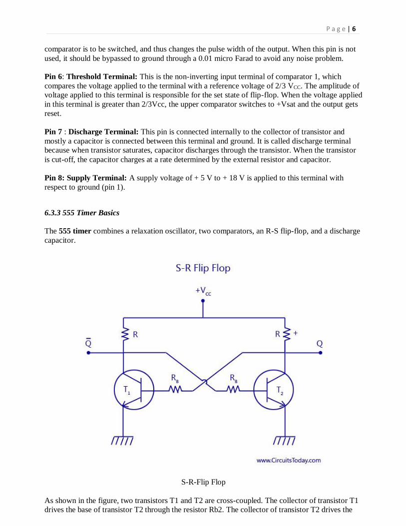
6.3.3 555 Timer Basics
The 555 timer combines a relaxation oscillator, two comparators, an R-S flip-flop, and a discharge
capacitor.
S-R-Flip Flop
As shown in the figure, two transistors T1 and T2 are cross-coupled. The collector of transistor T1
drives the base of transistor T2 through the resistor Rb2. The collector of transistor T2 drives the

P a g e | 7
base of transistor T1 through resistor Rb1. When one of the transistors is in the saturated state, the
other transistor will be in the cut-off state. If we consider the transistor T1 to be saturated, then the
collector voltage will be almost zero. Thus there will be a zero base drive for transistor T2 and will
go into cut-off state and its collector voltage approaches +Vcc. This voltage is applied to the base
of T1 and thus will keep it in saturation.
S-R Flip Flop Symbol
Now, if we consider the transistor T1 to be in the cut-off state, then the collector voltage of T1 will
be equal to +Vcc. This voltage will drive the base of the transistor T2 to saturation. Thus, the
saturated collector output of transistor T2 will be almost zero. This value when fed back to the base
of the transistor T1 will drive it to cut-off. Thus, the saturation and cut-off value of any one of the
transistors decides the high and low value of Q and its complement. By adding more components to
the circuit, an R-S flip-flop is obtained. R-S flip-flop is a circuit that can set the Q output to high or
reset it low. Incidentally, a complementary (opposite)Â output Q is available from the collector of
the other transistor. The schematic symbol for a S-R flip flop is also shown above. The circuit
latches in either the Q state or its complimentary state. A high value of S input sets the value of Q
to go high. A high value of R input resets the value of Q to low. Output Q remains in a given state
until it is triggered into the opposite state.

P a g e | 8
555 IC Timing Circuit
6.3.4 Basic Timing Concept
From the figure above, assuming the output of the S-R flip flop, Q to be high. This high value is
passed on to the base of the transistor, and the transistor gets saturated, thus producing a zero
voltage at the collector. The capacitor voltage is clamped at ground, that is, the capacitor C is
shorted and cannot charge.
The inverting input of the comparator is fed with a control voltage, and the non-inverting input is
fed with a threshold voltage. With R-S flip flop set, the saturated transistor holds the threshold
voltage at zero. The control voltage, however, is fixed at 2/3 VCC, that is, at 10 volts, because of
the voltage divider.
Suppose that a high voltage is applied to the R input. This resets the flip-flop R-Output Q goes low
and the transistor is cut-off. Capacitor C is now free to charge. As this capacitor C charges, the
threshold voltage rises. Eventually, the threshold voltage becomes slightly greater than (+ 10 V).
The output of the comparator then goes high, forcing the R S flip-flop to set. The high Q output
saturates the transistor, and this quickly discharges the capacitor. An exponential rise is across the
capacitor C, and a positive going pulse appears at the output Q. Thus capacitor voltage VC is
exponential while the output is rectangular. This is shown in the figure above.
6.3.5 555 IC Timer Block Diagram

P a g e | 9
555 IC Timer Block Diagram
The block diagram of a 555 timer is shown in the above figure. A 555 timer has two comparators,
which are basically 2 op-amps), an R-S flip-flop, two transistors and a resistive network.
Resistive network consists of three equal resistors and acts as a voltage divider.
Comparator 1 compares threshold voltage with a reference voltage + 2/3 VCC volts.
Comparator 2 compares the trigger voltage with a reference voltage + 1/3 VCC volts.
Output of both the comparators is supplied to the flip-flop. Flip-flop assumes its state according to
the output of the two compaÂrators. One of the two transistors is a discharge transistor of which
collector is connected to pin 7. This tranÂsistor saturates or cuts-off according to the output state
of the flip-flop. The saturated transisÂtor provides a discharge path to a capacitor conÂnected
externally. Base of another transistor is connected to a reset terminal. A pulse applied to this
terminal resets the whole timer irrespective of any input.
6.3.6 Working Principle
Refer Block Diagram of 555 timer IC given above:
The internal resistors act as a voltage divider network, providing (2/3)Vcc at the non-inverting
terminal of the upper comparator and (1/3)Vcc at the inverting terminal of the lower comparator. In
most applications, the control input is not used, so that the control voltage equals +(2/3) VCC.

P a g e | 10
Upper comparator has a threshold input (pin 6) and a control input (pin 5). Output of the upper
comparator is applied to set (S) input of the flip-flop. Whenever the threshold voltage exceeds the
control voltage, the upper comparator will set the flip-flop and its output is high. A high output
from the flip-flop when given to the base of the discharge transistor saturates it and thus discharges
the transistor that is connected externally to the discharge pin 7. The complementary signal out of
the flip-flop goes to pin 3, the output. The output available at pin 3 is low. These conditions will
prevail until lower comparator triggers the flip-flop. Even if the voltage at the threshold input falls
below (2/3) VCC, that is upper comparator cannot cause the flip-flop to change again. It means that
the upper comparator can only force the flip-flop’s output high.
To change the output of flip-flop to low, the voltage at the trigger input must fall below + (1/3)
Vcc. When this occurs, lower comparator triggers the flip-flop, forcing its output low. The low
output from the flip-flop turns the discharge transistor off and forces the power amplifier to output
a high. These conditions will continue independent of the voltage on the trigger input. Lower
comparator can only cause the flip-flop to output low.
From the above discussion, it is concluded that for the having low output from the timer 555, the
voltage on the threshold input must exceed the control voltage or + (2/3) VCC. This also turns the
discharge transistor on. To force the output from the timer high, the voltage on the trigger input
must drop below +(1/3) VCC. This turns the discharge transistor off.
A voltage may be applied to the control input to change the levels at which the switching occurs.
When not in use, a 0.01 nano Farad capacitor should be connected between pin 5 and ground to
prevent noise coupled onto this pin from causing false triggering.
Connecting the reset (pin 4) to a logic low will place a high on the output of flip-flop. The
discharge transistor will go on and the power amplifier will output a low. This condition will
continue until reset is taken high. This allows the synchronization or resetting of the circuit’s
operation. When not in use, reset should be tied to +VCC.
6.3.7 Applications of 555 Timer circuits
To know more about applications of 555 Timer IC take a look at the following posts:
555 TIMER AS AN ASTABLE MULTIVIRATOR
555 TIMER AS A MONOSTABLE MULTIVIBRATOR
555 TIMER OSCILLATOR
555 TIMER – RAMP GENERATOR
555 TIMER PROJECTS
6.4 IC 555 AS MONOSTABLE MULTIVIBRATOR
A monostable multivibrator (MMV) often called a one-shot multivibrator, is a pulse generator
circuit in which the duration of the pulse is determined by the R-C network,connected externally to
the 555 timer. In such a vibrator, one state of output is stable while the other is quasi-stable
(unstable). For auto-triggering of output from quasi-stable state to stable state energy is stored by

P a g e | 11
an externally connected capaciÂtor C to a reference level. The time taken in storage determines the
pulse width. The transition of output from stable state to quasi-stable state is accomÂplished by
external triggering. The schematic of a 555 timer in monostable mode of operation is shown in
figure.
555-timer-monostable-multivibrator
6.4.1 Monostable Multivibrator Circuit details
Pin 1 is grounded. Trigger input is applied to pin 2. In quiescent condition of output this input is
kept at + VCC. To obtain transition of output from stable state to quasi-stable state, a negative-going
pulse of narrow width (a width smaller than expected pulse width of output waveform)Â and
 amplitude of greater than + 2/3 VCC is applied to pin 2. Output is taken from pin 3. Pin 4 is
usually connected to + VCC to avoid accidental reset. Pin 5 is grounded through a 0.01 u F capacitor
to avoid noise problem. Pin 6 (threshold) is shorted to pin 7. A resistor RA is connected between
pins 6 and 8. At pins 7 a discharge capacitor is connected while pin 8 is connected to supply VCC.
6.4.2 555 IC Monostable Multivibrator Operation.

P a g e | 12
555 monostable-multivibrator-operation
The operation of the circuit is explained below:
Initially, when the output at pin 3 is low i.e. the circuit is in a stable state, the transistor is on and
capacitor- C is shorted to ground. When a negative pulse is applied to pin 2, the trigger input falls
below +1/3 VCC, the output of comparator goes high which resets the flip-flop and consequently the
transistor turns off and the output at pin 3 goes high. This is the transition of the output from stable
to quasi-stable state, as shown in figure. As the discharge transistor is cutÂoff, the capacitor C
begins charging toward +VCC through resistance RA with a time constant equal to RAC. When the
increasing capacitor voltage becomes slightly greater than +2/3 VCC, the output of comparator 1
goes high, which sets the flip-flop. The transistor goes to saturation, thereby discharging the
capacitor C and the output of the timer goes low, as illustrated in figure.
Thus the output returns back to stable state from quasi-stable state.
The output of the Monostable Multivibrator remains low until a trigger pulse is again applied. Then
the cycle repeats. Trigger input, output voltage and capacitor voltage waveforms are shown in
figure.
6.4.3 Monostable Multivibrator Design Using 555 timer IC
The capacitor C has to charge through resistance RA. The larger the time constant RAC, the longer
it takes for the capacitor voltage to reach +2/3VCC.
In other words, the RC time constant controls the width of the output pulse. The time during which
the timer output remains high is given as
tp = 1.0986 RAC where RA is in ohms and C is in farads. The above relation is derived as below. Voltage across the
capacitor at any instant during charging period is given as
vc = VCC (1- e-t/RAC)
Substituting vc = 2/3 VCC in above equation we get the time taken by the capacitor to charge from 0
to +2/3VCC.
So +2/3VCC. = VCC. (1 – e–t/RAC)  or  t – RAC loge 3 = 1.0986 RAC
So pulse width, tP = 1.0986 RAC s 1.1 RAC
The pulse width of the circuit may range from micro-seconds to many seconds. This circuit is
widely used in industry for many different timing applications.

P a g e | 13
QUESTIONS:
MULTIPLE CHOICE QUESTIONS:
1)which of following is multivibrator:
(a) astable (b) bistable
(c) monostable (d)all
2) which of following is timer?
(a) 555 (b) ) 741
(c) 8085 (d) none of the above
SHORT ANSWER TYPES QUESTIONS:
1) What is switch?
2) IC 555works as……………..
3) What do you mean by multivibrator?
4) What is function of timer?
5) Write three types of multivibrator.
LONG ANSWER TYPES QUESTIONS:
1) Explain in detail IC 555 as monostable multivibrator.
2) Explain in detail transistor as a switch.

P a g e | 14


