Download - DPs/DPD series DP-sP series
Pockels cellsPockels cells Drivers & HigH voltage suPPlies
Pulse Picking & Q-switcHing
Pockels cells
3.7 EKSMA OPTICS • Tel.: +370 5 272 99 00 • Fax: +370 5 272 92 99 • [email protected] • www.eksmaoptics.com
Pockels cells Drivers & HigH voltage suPPlies
● fast HV rise/fall time <4 – 8 ns● HV pulse amplitude up to 3.6 kV● Pulse repetition rate
up to 3.5 MHz
caviTy DuMPing & Pulse PicKing PocKels cell Drivers
DPs/DPD series DP-sP series
DPD series Pockels cell drivers are designed for wide range of applications and operating modes. Repetition rate can be up to 500 kHz for standard range of drivers, up to 1 MHz enhanced and up to 3.5 MHz high rate. standard range of possible pulse durations is from 100 ns to 5 μs. it can be extended to infinity using pulse regeneration technique. connection diagram can be PuSH-PuLL configura-tion using stand-alone driver, as well as FuLL BRiDGe using two drivers for one Pockels cell. FuLL BRiDGe configuration gives such advantages as repetition rate doubling to reach up to 7 MHz rate, pulse duration shortening down to zero or volt-age doubling on pockels cell.
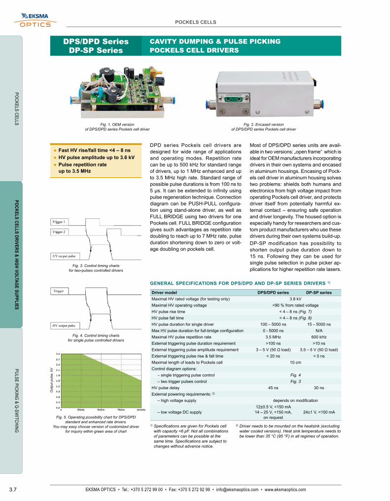
Most of DPS/DPD series units are avail-able in two versions: „open frame“ which is ideal for oeM manufacturers incorporating drivers in their own systems and encased in aluminum housings. encasing of Pock-els cell driver in aluminum housing solves two problems: shields both humans and electronics from high voltage impact from operating Pockels cell driver, and protects driver itself from potentially harmful ex-ternal contact – ensuring safe operation and driver longevity. The housed option is especially handy for researchers and cus-tom product manufacturers who use these drivers during their own systems build-up.DP-sP modification has possibility to shorten output pulse duration down to 15 ns. Following they can be used for single pulse selection in pulse picker ap-plications for higher repetition rate lasers.
Fig. 1. OEM version of DPS/DPD series Pockels cell driver
Fig. 2. Encased version of DPS/DPD series Pockels cell driver
GeneRal sPecifications foR dPs/dPd and dP-sP seRies dRiVeRs 1)
driver model dPs/dPd series dP-sP seriesMaximal HV rated voltage (for testing only) 3.8 kVMaximal HV operating voltage <90 % from rated voltageHV pulse rise time < 4 – 8 ns (Fig. 7)HV pulse fall time < 4 – 8 ns (Fig. 8)HV pulse duration for single driver 100 – 5000 ns 15 – 5000 nsMax HV pulse duration for full-bridge configuration 0 - 5000 ns N/AMaximal HV pulse repetition rate 3.5 MHz 600 kHzexternal triggering pulse duration requirement >100 ns >10 nsexternal triggering pulse amplitude requirement 3 – 5 V (50 Ω load) 3.5 – 5 V (50 Ω load)external triggering pulse rise & fall time < 20 ns < 5 nsMaximal length of leads to Pockels cell 10 cmcontrol diagram options:
– single triggering pulse control Fig. 4– two trigger pulses control Fig. 3
HV pulse delay 45 ns 30 nsexternal powering requirements: 2)
– high voltage supply depends on modification
– low voltage Dc supply12±0.5 V, <150 mA
14 – 25 V, <150 mA, on request
24±1 V, <150 mA
1) Specifications are given for Pockels cell with capacity <6 pF. Not all combinations of parameters can be possible at the same time. Specifications are subject to changes without advance notice.
2) Driver needs to be mounted on the heatsink (excluding water cooled versions). Heat sink temperature needs to be lower than 35 °C (95 °F) in all regimes of operation.
Fig. 5. Operating possibility chart for DPS/DPD standard and enhanced rate drivers.
You may easy choose version of customized driver for inquiry within green area of chart
Out
put p
ulse
, kV
Fig. 3. Control timing charts for two-pulses controlled drivers
Fig. 4. Control timing charts for single pulse controlled drivers
Pock
els
cell
sPo
ckel
s ce
lls
Driv
ers
& Hi
gH v
olta
ge s
uPPl
ies
Puls
e Pi
ckin
g &
Q-sw
itcH
ing
3.8Visit www.eksmaoptics.com for new products and prices
Pock
els
cell
s Dr
iver
s &
HigH
vol
tage
suP
Plie
s
POCKeLS CeLLS DRiVeRS & HiGH VOLtAGe SuPPLieS
Fig. 8. Typical falling front of output pulse in detailFig. 7. Typical rising front of output pulse in detailFig. 6. Typical output pulse shape
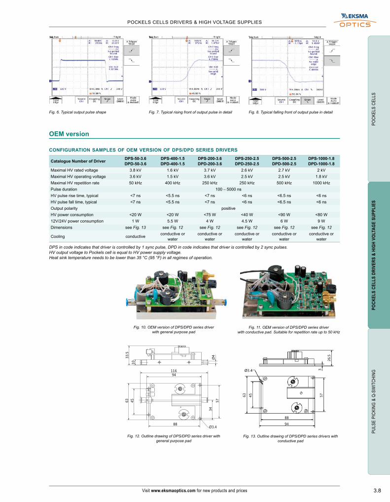
Fig. 11. OEM version of DPS/DPD series driver with conductive pad. Suitable for repetition rate up to 50 kHz
Fig. 10. OEM version of DPS/DPD series driver with general purpose pad
Fig. 13. Outline drawing of DPS/DPD series drivers with conductive pad
Fig. 12. Outline drawing of DPS/DPD series driver with general purpose pad
3
63
45
57
88
94
Ø .43
26.5
confiGuRation saMPles of oeM VeRsion of dPs/dPd seRies dRiVeRs
catalogue number of driver dPs-50-3.6 dPd-50-3.6
dPs-400-1.5 dPd-400-1.5
dPs-200-3.6 dPd-200-3.6
dPs-250-2.5 dPd-250-2.5
dPs-500-2.5 dPd-500-2.5
dPs-1000-1.8 dPd-1000-1.8
Maximal HV rated voltage 3.8 kV 1.6 kV 3.7 kV 2.6 kV 2.7 kV 2 kVMaximal HV operating voltage 3.6 kV 1.5 kV 3.6 kV 2.5 kV 2.5 kV 1.8 kVMaximal HV repetition rate 50 kHz 400 kHz 250 kHz 250 kHz 500 kHz 1000 kHzPulse duration 100 – 5000 nsHV pulse rise time, typical <7 ns <5.5 ns <7 ns <6 ns <6.5 ns <6 nsHV pulse fall time, typical <7 ns <5.5 ns <7 ns <6 ns <6.5 ns <6 nsoutput polarity positiveHV power consumption <20 W <20 W <75 W <40 W <90 W <80 W12V/24V power consumption 1 W 5.5 W 4 W 4.5 W 6 W 9 WDimensions see Fig. 13 see Fig. 12 see Fig. 12 see Fig. 12 see Fig. 12 see Fig. 12
cooling conductive conductive or water
conductive or water
conductive or water
conductive or water
conductive or water
DPS in code indicates that driver is controlled by 1 sync pulse, DPD in code indicates that driver is controlled by 2 sync pulses.HV output voltage to Pockels cell is equal to HV power supply voltage. Heat sink temperature needs to be lower than 35 °C (95 °F) in all regimes of operation.
63
116
33.5
94
88
57
45
10
Ø4
34
Ø .3 4
oeM version
Pockels cellsPockels cells Drivers & HigH voltage suPPlies
Pulse Picking & Q-switcHing
Pockels cells
3.9 EKSMA OPTICS • Tel.: +370 5 272 99 00 • Fax: +370 5 272 92 99 • [email protected] • www.eksmaoptics.com
Pockels cells Drivers & HigH voltage suPPlies
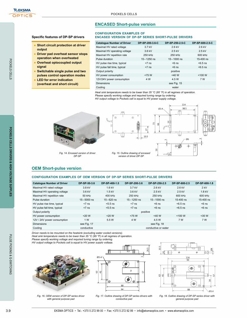
Fig. 14. Encased version of driverDP-SP
confiGuRation exaMPles of oeM VeRsion of dP-sP seRies sHoRt-Pulse dRiVeRs
catalogue number of driver dP-sP-50-3.6 dP-sP-400-1.5 dP-sP-200-3.6 dP-sP-250-2.5 dP-sP-600-2.5 dP-sP-600-1.8Maximal HV rated voltage 3.8 kV 1.6 kV 3.7 kV 2.6 kV 2.6 kV 2 kVMaximal HV operating voltage 3.6 kV 1.5 kV 3.6 kV 2.5 kV 2.5 kV 1.8 kVMaximal HV repetition rate 50 kHz 400 kHz 250 kHz 250 kHz 600 kHz 600 kHzPulse duration 15 – 5000 ns 15 – 620 ns 15 – 1250 ns 15 – 1000 ns 15-400 ns 15-400 nsHV pulse rise time, typical <7 ns <5.5 ns <7 ns <6 ns <6.5 ns <6 nsHV pulse fall time, typical <7 ns <5.5 ns <7 ns <6 ns <6.5 ns <6 nsoutput polarity positiveHV power consumption <20 W <20 W <75 W <40 W <100 W <35 W12V / 24V power consumption 1 W 5.5 W 4 W 4.5 W 7 W 7 WDimensions see Fig. 17 see Fig. 18cooling conductive conductive or water
Driver needs to be mounted on the heatsink (excluding water cooled versions).Heat sink temperature needs to be lower than 35 °C (95 °F) in all regimes of operation.Please specify working voltage and required tuning range by ordering.HV output voltage to Pockels cell is equal to HV power supply voltage.
confiGuRation exaMPles of encased VeRsion of dP-sP seRies sHoRt-Pulse dRiVeRs
catalogue number of driver dP-sP-200-3.6-c dP-sP-250-2.5-c dP-sP-600-2.5-cMaximal HV rated voltage 3.7 kV 2.6 kV 2.6 kVMaximal HV operating voltage 3.6 kV 2.5 kV 2.5 kVMaximal HV repetition rate 250 kHz 250 kHz 600 kHzPulse duration 15 – 1250 ns 15 – 1000 ns 15-400 nsHV pulse rise time, typical <7 ns <6 ns <6.5 nsHV pulse fall time, typical <7 ns <6 ns <6.5 nsoutput polarity positiveHV power consumption <75 W <40 W <100 W12V/24V power consumption 4 W 4.5 W 7 WDimensions see Fig. 15cooling water
Heat sink temperature needs to be lower than 35 °C (95 °F) in all regimes of operation.Please specify working voltage and required tuning range by ordering.HV output voltage to Pockels cell is equal to HV power supply voltage.
Fig. 16. OEM version of DP-SP series driver with general purpose pad
Fig. 17. Outline drawing of DP-SP series drivers with conductive pad
Fig. 18. Outline drawing of DP-SP series driver with general purpose pad
3
63
45
57
88
94
Ø .43
26.5
63
116
33.5
94
88
57
45
10
Ø4
34
Ø .3 4
oeM short-pulse version
encased short-pulse version
114
98 5.
73
66
Ø .3 4
3
50
27
10 5.
3Ø6
114
98 5.
73
66
Ø .3 4
3
50
27
10 5.
3Ø6
114
98 5.
73
66
Ø .3 4
3
50
27
10 5.
3Ø6
Fig. 15. Outline drawing of encased version of driver DP-SP
Specific features of DP-SP drivers
● short circuit protection at driver output
● driver pad overheat sensor stops operation when overheated
● overheat optocoupled output signal
● switchable single pulse and two pulses control operation modes
● led for error indication (overheat and short circuit)

Pock
els
cell
sPo
ckel
s ce
lls
Driv
ers
& Hi
gH v
olta
ge s
uPPl
ies
Puls
e Pi
ckin
g &
Q-sw
itcH
ing
3.10Visit www.eksmaoptics.com for new products and prices
Pock
els
cell
s Dr
iver
s &
HigH
vol
tage
suP
Plie
s
POCKeLS CeLLS DRiVeRS & HiGH VOLtAGe SuPPLieS
Fig. 22. Outline drawing of encased version of driver DPS/DPD models Fig. 21. Encased version of driver DPS/DPD models.
Water cooled version
135
58
Ø4 5.
48
5.
Ø6
158
69
81
145
3
68
145
31
135
58
Ø4 5.
48
5.
Ø6
158
69
81
145
3
68
145
31
encased version (bipolar drivers)
confiGuRation saMPles of encased VeRsion of dPs/dPd seRies BiPolaR dRiVeRs
catalogue number of driver dPs-250-5.2-aldPd-250-5.2-al
dPs-300-4.6-aldPd-300-4.6-al
dPs-350-4-aldPd-350-4-al
dPs-1000-2.9-aidPd-1000-2.9-ai
Maximal HV rated voltage 5.3 kV 4.8 kV 4.2 kV 3.0 kVMaximal HV operating voltage 5.2 kV 4.6 kV 4.0 kV 2.9 kVMaximal HV repetition rate 250 kHz 300 kHz 350 kHz 1000 kHzPulse duration 120 – 5000 nsHV pulse rise time, typical <8.5 ns <8 ns <7.5 ns <7.5 nsHV pulse fall time, typical <8.5 ns <8 ns <7.5 ns <7.5 nsoutput polarity bipolarHV power consumption <100 W <100 W <100 W <120 W12V/24V power consumption 9 WDimensions see Fig. 22
cooling conductive or water
encased version (unipolar drivers)
Fig. 20. Outline drawing of encased version of driver DPS/DPD models DPS/DPD-200-xx,
DPS/DPD-250-xx, DPS/DPD-500-xx, DPS/DPD-1000-1.8
confiGuRation saMPles of encased VeRsion of dPs/dPd seRies uniPolaR dRiVeRs
catalogue number of driver dPs-200-3.6-al dPd-200-3.6-al
dPs-250-2.5-al dPd-250-2.5-al
dPs-500-2.5-al dPd-500-2.5-al
dPs-1000-1.8-al dPd-1000-1.8-al
Maximal HV rated voltage 3.7 kV 2.6 kV 2.7 kV 2 kVMaximal HV operating voltage 3.6 kV 2.5 kV 2.6 kV 1.8 kVMaximal HV repetition rate 250 kHz 250 kHz 500 kHz 1000 kHzPulse duration 120 – 5000 nsHV pulse rise time, typical <7 ns <6 ns <6.5 ns <6 nsHV pulse fall time, typical <7 ns <6 ns <6.5 ns <6 nsoutput polarity positiveHV power consumption <75 W <40 W <90 W <80 W12V/24V power consumption 4 W 4.5 W 6 W 9 WDimensions see Fig. 20cooling water
Fig. 19. Encased version of driver DPS/DPD models DPS/DPD-200-xx, DPS/DPD-250-xx, DPS/DPD-500-xx,
DPS/DPD-1000-1.8
Driver needs to be mounted on the heatsink (excluding water cooled versions). Heat sink temperature needs to be lower than 35 °C (95 °F) in all regimes of operation.HV output voltage to Pockels cell is equal to HV power supply voltage i.e. sum of positive and negative HV values.Please specify working voltage and required tuning range by ordering.
* Bipolar HV power supply HV2x60Wm is specifically designed for these drivers.
114
98 5.
73
66
Ø .3 4
3
50
27
10 5.
3Ø6
114
98 5.
73
66
Ø .3 4
3
50
27
10 5.
3Ø6
114
98 5.
73
66
Ø .3 4
3
50
27
10 5.
3Ø6
114
98 5.
73
66
Ø .3 4
3
50
27
10 5.
3Ø6
Pockels cellsPockels cells Drivers & HigH voltage suPPlies
Pulse Picking & Q-switcHing
Pockels cells
3.11 EKSMA OPTICS • Tel.: +370 5 272 99 00 • Fax: +370 5 272 92 99 • [email protected] • www.eksmaoptics.com
Pockels cells Drivers & HigH voltage suPPlies
confiGuRation exaMPles of full-BRidGe confiGuRation dRiVeRs
catalogue number of full-Bridge driver 2dPs-1000-2.5-al 2dPd-1000-2.5-al
2dPs-2000-1.6-al2dPd-2000-1.6-al
Base driver DPs-500-2.5 DPD-500-2.5
DPs-1000-1.6DPD-1000-1.6
Maximal HV operating voltage 2.4 kV 1.6 kVMaximal HV repetition rate 1000 kHz 2000 kHzHV pulse duration range 0 – 5000 nsHV pulse rise time <6.5 ns <6 nsHV pulse fall time <6.5 ns <6 nsMaximal capacitance of Pockels cell <6 pFHV power consumption <160 Wcase see Fig. 26cooling water
Fig. 25. Principle of 4-phase control of full-bridge driver configuration
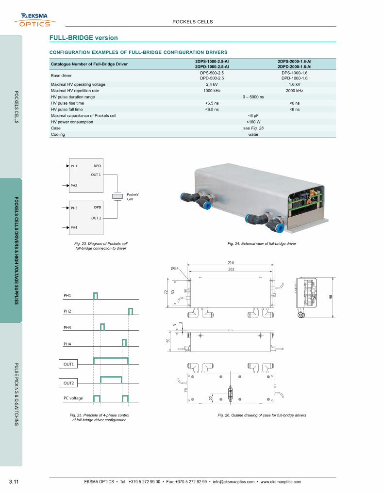
Fig. 23. Diagram of Pockels cell full-bridge connection to driver
Fig. 26. Outline drawing of case for full-bridge drivers
PH1
PH3
PH2
PH4
Pockels’
Cell
OUT 2
OUT 1
DPD
DPD
PH2
PH3
PH4
PC voltage
PH1
OUT1
OUT2
Fig. 24. External view of full-bridge driver
full-BRidGe version
210
202
72
60
Ø .3 4
3
50
22
3
98


