Development of a 24GHz fully integrated VCO
Saeid Ghassemi
Supervisors: Dipl.-Ing. Uwe Stehr (IMST GmbH)Prof. Dr. - Ing K. SolbachChair of Department of High Frequency Technique
University Duisburg - Essen
University of Duisburg-Essen

Wireless Communication
wireless LAN’s
GPS/satellite
Receivers
low-cost
Cellular Telephones
small sizelow power
small form
Development of a 24GHz fully integrated VCO

Voltage Controlled Oscillators
PLL-BasedApplications
Applications
Non-PLL BasedApplications
Development of a 24GHz fully integrated VCO

Voltage Controlled Oscillators
Base Station
Satellite CommunicationGPS & Navigation
Cell PhoneTelecommunication
LAN/WANMilitary
Applications
Development of a 24GHz fully integrated VCO

VCO in Digital & Analog Applications
Development of a 24GHz fully integrated VCO
VCO for High speed data link
VCO for Analog wirless system

Design Goals
Design integrated on-chip inductor optimized for low phase noise VCO Core Stable on-chip power amplifierThe matching between the core and PA and PA and load
Development of a 24GHz fully integrated VCO

Target Design Specifications
Frequency 23.9- 24.35 GHz Out put Power 6 dBmSupply Voltage 3.2V to 3.4V Supply Current <50mA Phase Noise <-70 dBc/Hz @ 100 KHz offset Tuning Voltage Range 0.4 to 2.8 V Temperature Range -40° C to 105° C Layout < 1
Development of a 24GHz fully integrated VCO

Some Theories
Development of a 24GHz fully integrated VCO
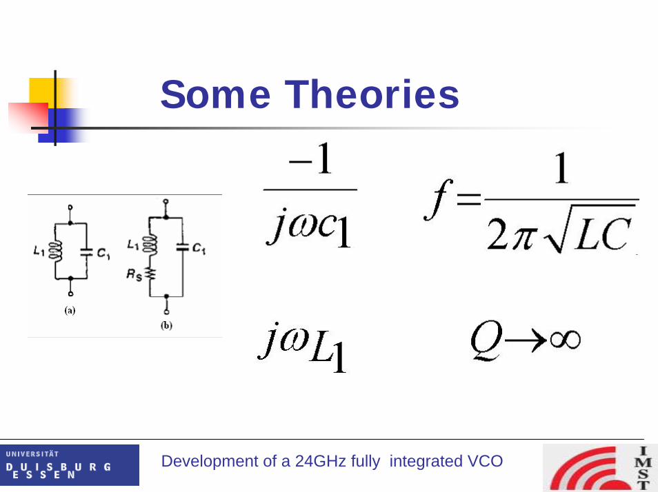
Some Theories
Development of a 24GHz fully integrated VCO
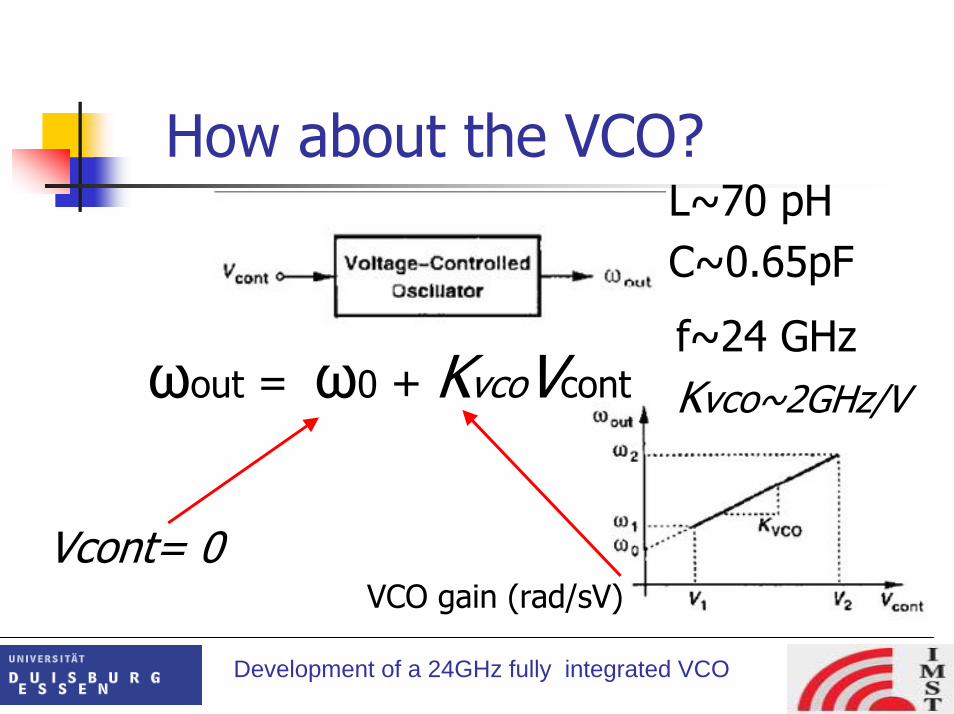
How about the VCO?
ωout = ω0 + KvcoVcont
Development of a 24GHz fully integrated VCO
Vcont= 0VCO gain (rad/sV)
L~70 pHC~0.65pF
f~24 GHzKvco~2GHz/V
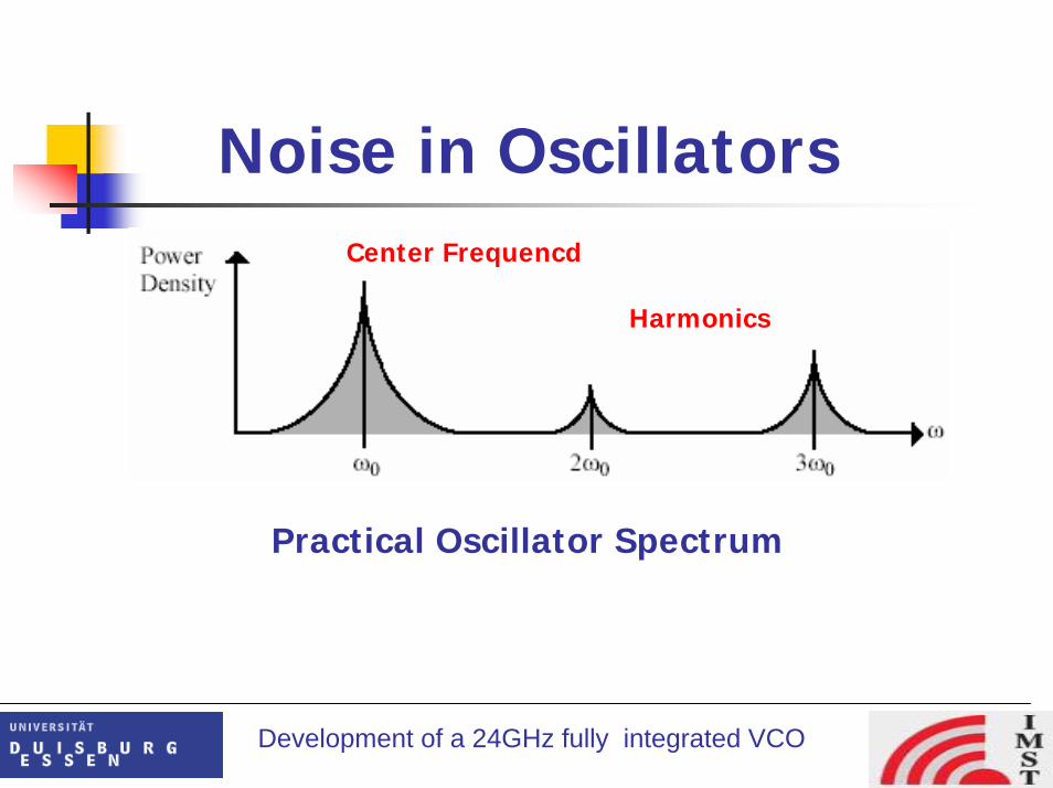
Noise in OscillatorsCenter Frequencd
Harmonics
Practical Oscillator Spectrum
Development of a 24GHz fully integrated VCO
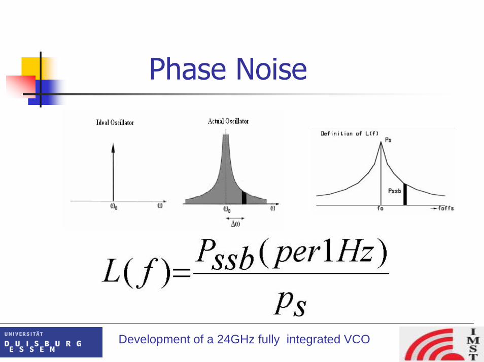
Phase Noise
Development of a 24GHz fully integrated VCO

Phase Noise
frequency modulation
mixes up to the oscillation frequency
flicker FM NoiseWhite FM Noise
flicker PM NoiseWhite PM Noise
Development of a 24GHz fully integrated VCO
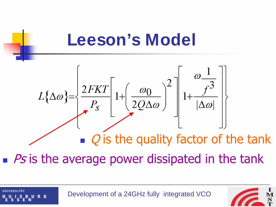
Leeson’s Model
Development of a 24GHz fully integrated VCO
Ps is the average power dissipated in the tank
Q is the quality factor of the tank
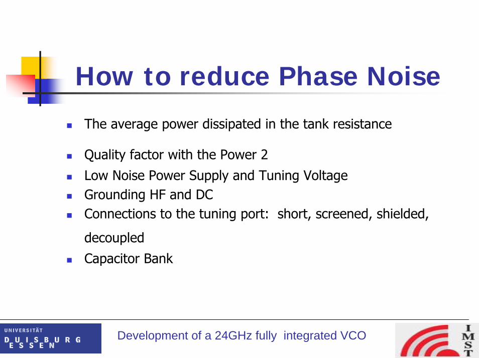
How to reduce Phase Noise
The average power dissipated in the tank resistance
Quality factor with the Power 2
Low Noise Power Supply and Tuning VoltageGrounding HF and DCConnections to the tuning port: short, screened, shielded,
decoupled
Capacitor Bank
Development of a 24GHz fully integrated VCO
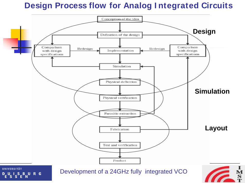
Design Process flow for Analog Integrated Circuits
Development of a 24GHz fully integrated VCO
Layout
Simulation
Design

The applied technologyB7HF200_8 200 GHz Bipolar technology
200 GHz SiGe /( silicon-germanium) bipolar process with copper
metallization for mixed analogue / digital HF applications
Development of a 24GHz fully integrated VCO
High speed and ultra high speed npn Transistors
Varactors MIM capacitors 3 kind of Resistors
No Inductor
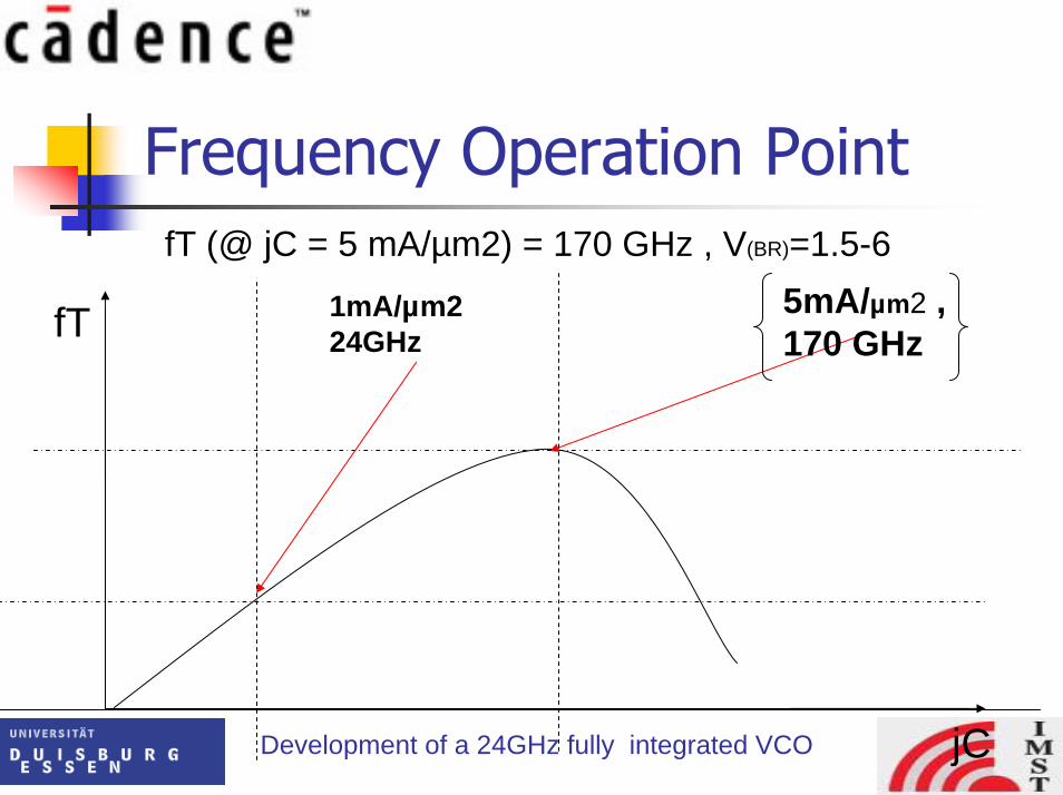
Frequency Operation Point
Development of a 24GHz fully integrated VCO
fT (@ jC = 5 mA/µm2) = 170 GHz , V(BR)=1.5-6
fT
jC
5mA/µm2 , 170 GHz
1mA/µm224GHz

Inductors
On-chip spiral inductors
Very non ideal behaviour
Rather low Q
Size depends on the currentWidth< 15 um
A S I T I C
Symmetric, Differential L=70pH Q=15
Development of a 24GHz fully integrated VCO

Losses in Integrated Inductors
Development of a 24GHz fully integrated VCO
low frequencies,
higher frequencies
metal & via resistance constant
Q directly proportional to frequency skin effect
Q proportional to Frequency and affectedbye the substrate.
Q is proportional to square root of Frequency.
A S I T I C
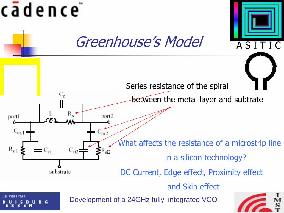
Greenhouse’s Model
Development of a 24GHz fully integrated VCO
Series resistance of the spiral
between the metal layer and subtrate
DC Current, Edge effect, Proximity effect
and Skin effect
What affects the resistance of a microstrip line
in a silicon technology?
A S I T I C

VCO Core
Tank Circuit
Negative resistancecross-coupled pairs
Current Source
Development of a 24GHz fully integrated VCO

Negative Resistance Circuit
Advantages :Simple topology Good for feeding differential circuits Good phase noise performance can be achieved, it can reject common mode noise,Has better power supply noise rejection,Easier to bias on-chip without any ideal ground available.
Development of a 24GHz fully integrated VCO
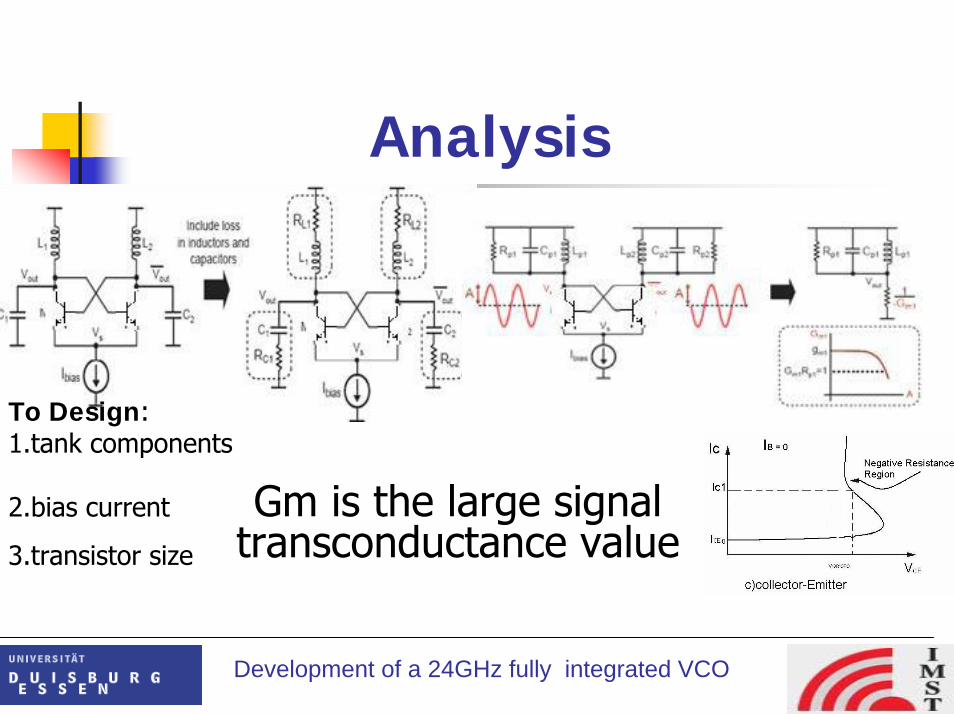
Analysis
Gm is the large signal transconductance value
To Design:1.tank components
2.bias current
3.transistor size
Development of a 24GHz fully integrated VCO

Simulation Results
Development of a 24GHz fully integrated VCO
1.8 V p-p

Amplifier
Biasingin
Class A
Disadvntage:Conduction
angel
Battery
To decouple the
Core & external load.
To provide sufficient output power.
Active devices

Fourier analysis of the Current wave form
20Log V = 6dBm , V=0.44
Ac denn 0.44*1.4 = 0.63 v Amplitude
10Log(P)= 6dBm p=4mW
P=R*I^2 I=9mA
Development of a 24GHz fully integrated VCO

Stability CalculationsThe circuit is Unconditionally Stable if
and
for all values of RS and RL
Development of a 24GHz fully integrated VCO

Stability CirclesDrawing the locus of the source and load terminations on the Smith Chart
for Source stability Circle
for Load stability Circle
Development of a 24GHz fully integrated VCO

Stability Circles
Load stability
Circle
Source stability
Circle
S22> 1 The area including the centre is unstable
S22< 1 The area including the canter is stable
S11> 1S11< 1
The area including the centre is unstable
The area including the centre is stable
Development of a 24GHz fully integrated VCO

How to make an Amplifier Stable?
Add a resistor( Seri or Parallel)
Feed back Amplifier
Development of a 24GHz fully integrated VCO

The Complete Circuit
Development of a 24GHz fully integrated VCO
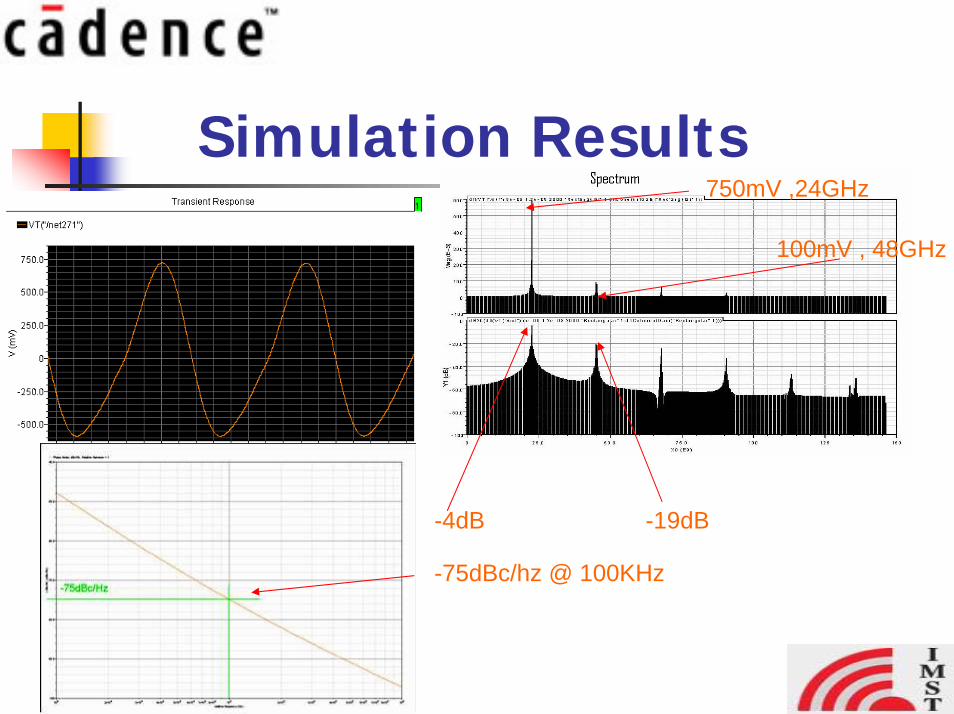
Simulation Results750mV ,24GHz
100mV , 48GHz
-4dB -19dB
-75dBc/hz @ 100KHz
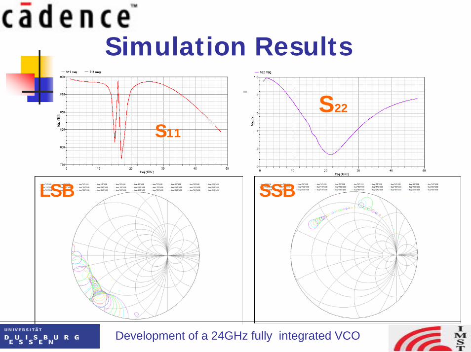
Simulation Results
S22
S11
LSB SSB
Development of a 24GHz fully integrated VCO

Layout
Development of a 24GHz fully integrated VCO
0.7
Symmetric
ParasiticsExtraction

Thanks for the attention


