
Data Sheet
S6D0128
176 RGB X 240 DOT 1-CHIP DRIVER IC WITH INTERNAL GRAM FOR 262,144 Colors TFT-LCD
November 02, 2005
Ver. 1.0
Prepared by Checked by Approved by
Su-Nam, Park
Byoung-Ha, Kim
Yhong-Deug, Ma
System LSI Division Semiconductor Business
SAMSUNG ELECTRONICS CO., LTD.
Contents in this document are subject to change without notice. No part of this document may be reproduced or
transmitted in any form or by any means, electronic or mechanical, for any purpose, without the express written
permission of LCD Driver IC Team.

176-RGB X 240-DOT 1-CHIP DRIVER IC FOR 262,144-COLOR TFT-LCD DISPLAY S6D0128
2
CONTENTS
CONTENTS ................................................................................................................................................................2
INTRODUCTION.........................................................................................................................................................4
FEATURES.................................................................................................................................................................5
BLOCK DIAGRAM .....................................................................................................................................................6
PAD CONFIGURATION .............................................................................................................................................7
ALIGN KEY CONFIGURATION AND COORDINATE ........................................................................................9
PAD CENTER COORDINATES...............................................................................................................................10
PIN DESCRIPTION...................................................................................................................................................17
POWER SUPPLY PIN.......................................................................................................................................17
SYSTEM/RGB INTERFACE PIN ......................................................................................................................20
DISPLAY PIN ....................................................................................................................................................22
MISCELLANEOUS PIN.....................................................................................................................................22
FUNCTIONAL DESCRIPTION .................................................................................................................................23
SYSTEM INTERFACE ......................................................................................................................................23
EXTERNAL INTERFACE (RGB-I/F, VSYNC-I/F) .............................................................................................24
ADDRESS COUNTER (AC)..............................................................................................................................24
GRAPHICS RAM (GRAM) ................................................................................................................................24
GRAYSCALE VOLTAGE GENERATOR ..........................................................................................................24
TIMING GENERATOR......................................................................................................................................24
OSCILLATION CIRCUIT (OSC)........................................................................................................................24
SOURCE DRIVER CIRCUIT.............................................................................................................................25
GATE DRIVER CIRCUIT ..................................................................................................................................25
SYSTEM/RGB INTERFACE AND GRAM ADDRESS SETTING ............................................................................26
GRAM ADDRESS SETTING (SS=”0”)..............................................................................................................26
SYSTEM INTERFACE ......................................................................................................................................27
RGB INTERFACE .............................................................................................................................................30
GRAM ADDRESS SETTING (SS=”1”)..............................................................................................................31
SYSTEM INTERFACE ......................................................................................................................................32
RGB INTERFACE .............................................................................................................................................35
INSTRUCTIONS .......................................................................................................................................................36
INSTRUCTION TABLE .....................................................................................................................................38
INSTRUCTION DESCRIPTIONS......................................................................................................................40
RESET FUNCTION...................................................................................................................................................77
POWER SUPPLY CIRCUIT .....................................................................................................................................78
PATTERN DIAGRAMS FOR VOLTAGE SETTING.................................................................................................79
SET UP FLOW OF POWER.....................................................................................................................................80
EXTERNAL POWER ON / OFF SEQUENCE ..........................................................................................................81
SET UP FLOW OF DISPLAY...................................................................................................................................82
VOLTAGE REGULATION FUNCTION ....................................................................................................................84
INTERFACE SPECIFICATION.................................................................................................................................85
S6D0128 176-RGB X 240-DOT 1-CHIP DRIVER IC FOR 262,144-COLOR TFT-LCD DISPLAY
3
SYSTEM INTERFACE .............................................................................................................................................86
68/80-SYSTEM 18-BIT BUS INTERFACE ....................................................................................................... 86
68/80-SYSTEM 16-BIT BUS INTERFACE ....................................................................................................... 87
68/80-SYSTEM 9-BIT BUS INTERFACE ......................................................................................................... 89
68/80-SYSTEM 8-BIT BUS INTERFACE ......................................................................................................... 90
SERIAL DATA TRANSFER.....................................................................................................................................93
VSYNC INTERFACE................................................................................................................................................97
EXTERNAL DISPLAY INTERFACE ......................................................................................................................101
RGB INTERFACE........................................................................................................................................... 101
ENABLE SIGNALS ......................................................................................................................................... 102
RGB INTERFACE TIMING ............................................................................................................................. 103
MOTION PICTURE DISPLAY......................................................................................................................... 105
RAM ACCESS VIA RGB INTERFACE AND SYSTEM INTERFACE ............................................................. 105
6-BIT RGB INTERFACE ................................................................................................................................. 106
16-BIT RGB INTERFACE ............................................................................................................................... 107
18-BIT RGB INTERFACE ............................................................................................................................... 108
USAGE ON EXTERNAL DISPLAY INTERFACE ........................................................................................... 108
WINDOW ADDRESS FUNCTION..........................................................................................................................110
GATE DRIVER SCAN MODE SETTING ...............................................................................................................111
GAMMA ADJUSTMENT FUNCTION ....................................................................................................................112
STRUCTURE OF GRAYSCALE AMPLIFIER .......................................................................................................113
GAMMA ADJUSTMENT REGISTER.....................................................................................................................115
LADDER RESISTOR/8 TO 1 SELECTOR.............................................................................................................117
VARIABLE RESISTOR ................................................................................................................................... 117
THE 8 TO 1 SELECTOR ................................................................................................................................ 118
THE 8-COLOR DISPLAY MODE...........................................................................................................................124
SYSTEM STRUCTURE EXAMPLE .......................................................................................................................126
OSCILLATOR CIRCUIT.........................................................................................................................................127
1-RASTER-ROW REVERSED AC DRIVE.............................................................................................................128
A/C TIMING ............................................................................................................................................................129
FRAME FREQUENCY ADJUSTING FUNCTION..................................................................................................130
RELATIONSHIP BETWEEN LCD DRIVE DUTY AND FRAME FREQUENCY.............................................. 130
SCREEN-DIVISION DRIVING FUNCTION............................................................................................................131
RESTRICTION ON THE 1ST
/2ND
SCREEN DRIVING POSITION REGISTER SETTINGS ...................................132
APPLICATION CIRCUIT........................................................................................................................................134
SPECIFICATIONS..................................................................................................................................................135
ABSOLUTE MAXIMUM RATINGS ................................................................................................................. 135
DC CHARACTERISTICS................................................................................................................................ 136
AC CHARACTERISTICS ................................................................................................................................ 138
REVISION HISTORY..............................................................................................................................................145
NOTICE ..................................................................................................................................................................147
176-RGB X 240-DOT 1-CHIP DRIVER IC FOR 262,144-COLOR TFT-LCD DISPLAY S6D0128
4
INTRODUCTION
The S6D0128 is 1-chip solution for TFT-LCD panel: source driver with built-in memory, gate driver, power IC are
integrated on one chip. This IC can display to a maximum of 176-RGB x 240-dot graphics on 260k-color TFT panel.
The S6D0128 also supports 18-/16-/9-/8-bit high-speed bus interface and high-speed RAM-write functions enable
efficient data transfer and high-speed rewriting of data to the internal GRAM.
The motion picture area can be specified in internal GRAM by window function. The specified window area can be
updated selectively, so that motion picture is able to be displayed simultaneously independent of still picture area.
The S6D0128 has various functions for reducing the power consumption of a LCD system: operating at low voltage
(1.8V), register-controlled power-save mode, low-current mode, partial display mode and so on. The IC has internal
GRAM to store 176-RGB x 240-dot 260k-color image and internal step-up circuit that generates the LCD driving
voltage, breeder resistance and the voltage follower circuit for LCD driver.
This LSI is suitable for any medium-sized or small portable mobile solution requiring long-term driving capabilities,
such as digital cellular phones supporting a web browser, bi-directional pagers, and small PDAs.
S6D0128 176-RGB X 240-DOT 1-CHIP DRIVER IC FOR 262,144-COLOR TFT-LCD DISPLAY
5
FEATURES
176-RGB x 240-dot TFT-LCD display controller/driver IC for 262,144 colors (528 channel-source driver/
240 channel-gate driver)
18-/16-/9-/8-bit high-speed parallel bus interface (80- and 68- system) and serial peripheral interface (SPI)
18-/16-/6-bit RGB interface
VSYNC interface
Writing to a window-RAM address area by using a window-address function
Various color-display control functions
− 262,144 colors can be displayed at the same time (including gamma adjust)
− Vertical scroll display function in raster-row units
Internal RAM capacity: 176 x 18 x 240 = 760,320 bits
Low-power operation supports:
− Power-save mode: standby mode, sleep mode
− Partial display of two screens in any position
− Maximum 6-times step-up circuit for generating driving voltage
− Voltage followers to decrease direct current flow in the LCD drive breeder-resistors
− Charge sharing function for the switching performance of step-up circuits and operational amplifiers
1-raster row inversion drive (Reverse the polarity of driving voltage in every selected raster row)
Internal oscillation circuit and external hardware reset
Structure for TFT-display retention volume (only for Cst)
Alternating functions for TFT-LCD counter-electrode power
− Line alternating drive of VCOM.
Internal power supply circuit
− Step-up circuit: four to six times positive-polarity, two to five times negative-polarity
− Adjustment of VCOM amplitude: internal 64-level digital potentiometer
Operating voltage
• Apply voltage
− VDD = 1.65 to 1.95 [V] (Typical 1.8 [V])
− VDD3 = 1.65 to 3.3 [V]
When VDD3 = 1.65 to 1.95 [V], VDD = VDD3 (No using Internal Regulator, PREGB = “VDD3”)
When VDD3 > 1.95 [V] (Using Internal Regulator, PREGB = “VSS”)
− VCI to VSS = 2.5 to 3.3 V (internal reference power-supply voltage)
• Generate voltage
− For the source driver: AVDD to VSS = 4.0 to 5.5V (power supply for driving circuits)
GVDD to VSS = 3.5 to 5.0V (reference power supply for grayscale voltages)
− For the gate driver: VGH to VGL = 10.5 to 30V, VGH to VSS = +7.0 to +16.5V,
VGL to VSS = -13.75 to -3.5 V
− For the step up circuit: VCI1 to VSS = 1.75 to 2.75 V (refer to Instruction Description)
− For the TFT-LCD counter electrode: VCOM amplitude (max) = 6.0V,
VCOMH to VSS = 3.0 to 5.0V,
VCOML to VSS = (VCL+0.5) V to 1.0V
(The value of C31 ITO resistance must be 50Ω and below.)
S6D0128 is released COG type package format only.

176-RGB X 240-DOT 1-CHIP DRIVER IC FOR 262,144-COLOR TFT-LCD DISPLAY S6D0128
6
BLOCK DIAGRAM
Figure 1. S6D0128 Block Diagram

S6D0128 176-RGB X 240-DOT 1-CHIP DRIVER IC FOR 262,144-COLOR TFT-LCD DISPLAY
7
PAD CONFIGURATION
S6D0128
No. 1
No. 246
No. 283
No. 1009No. 1045
DUMMY<*6>VCOM
<*6>VGH<*3>C21P<*3>C21M
<*4>C22P
<*3>C22M<*9>VGL<*2>DUMMYVDD3OPREGB
<*9>VCI
<*5>VCI1
<*8>C11P<*8>C11M
<*4>VCL
<*6>VDD3
<*2>VDDIO<*8>VDD<*2>VDDO
<*5>VDDM
GMON
VSS3OIM<0>
IM<1>
VDD3OIM<2>
IM<3>
<*8>AVSS
VSS3O
<*3>VSSA
RESETB
<*5>VSSM
<*5>VSS<*2>VSSO
<*8>VSSC
<*2>VGS
DB<17>DB<16>DB<15>
DB<14>
DB<13>DB<12>
DB<11>
DB<10>
DB<9>
DB<8>
DB<7>DB<6>DB<5>
DB<3>
DB<2>
DB<1>DB<0>
E_RDB
RW_WRB
RS
CSB
VSYNC
HSYNC
DOTCLKENABLE
TAD9TAD8
TAD7TAD6
TAD5TAD4TAD3TAD2
TAD1TAD0
VSS3OTEST_MUX
TEST_GRAYVDD3O
DISPTMG
PREC
ECS
M
FLMCL1
TSOOSC1OSC2
DUMMY
<*6>VCOM
<*2>VREF0<*2>VREFI
RESETB
CONTACT1
CONTACT2
DUMMY
VCI_REF
<*2>VCOML<*2>VCOMH<*2>GVDD
<*2>VCOMR
DUMMY
VCIR
Top View
Y
X
(0,0
)
VSS3O
VSS3O
VSS3OSDI
SDO
VSS3O
VDD3O
VSS3O
VDD3O
DB<4>
TSI0TSI1TEST
FUSE_EN
<*3>VSS3
ATEST
<*6>AVDD
<*5>C31P<*5>C31M
DUMMY
DUMMY
DUMMY G<2>
G<4>
G<6>
G<8> G<10>
DUMMY
G<54>
G<56> G<58>
G<60> G<62>
DUMMY
DUMMY
G<64>DUMMY
DUMMY
DUMMY
G<68>G<66>
G<72>G<70>
G<236>G<234>
G<232>
G<240>G<238>
DUMMYDUMMY
DUMMYDUMMY
DUMMYDUMMY
S<527>S<528>
S<525>S<526>
S<523>S<524>
S<270>S<271>
S<272>
S<268>S<269>
S<266>S<267>
S<264>S<265>
S<262>S<263>
S<260>S<261>
S<258>S<259>
S<256>S<257>
S<3>S<4>
S<5>
S<1>S<2>
DUMMYDUMMY
DUMMYDUMMY
DUMMYDUMMY
G<239>DUMMY
G<235>G<237>
G<231>G<233>
G<71>
G<67>G<69>
G<63>G<65>
DUMMYDUMMY
DUMMY
DUMMY
G<53> G<55>
G<57> G<59>
G<61>
DUMMY
DUMMY
DUMMY
DUMMY
DUMMY
G<1>G<3>
G<5>
G<7>
G<9>
<*#>, # is duplicate number.
Figure 2. Pad Configuration

176-RGB X 240-DOT 1-CHIP DRIVER IC FOR 262,144-COLOR TFT-LCD DISPLAY S6D0128
8
Table 1. S6D0128 Pad Dimensions
Size Items Pad name.
X Y Unit
Chip size1) - 18,190 1,450
Input PAD (1-246) 48 86
Source (375-916) 22 100
Gate (247-283,
1009-1045) 100 22
Bumped Pad
Size Output
Pad Gate (284-375,
917-1008) 22 100
Bumped Pad
Height All Pad
15 ± 3
um
NOTES:
Scribe lane included in this chip size (Scribe lane: 100um)

S6D0128 176-RGB X 240-DOT 1-CHIP DRIVER IC FOR 262,144-COLOR TFT-LCD DISPLAY
9
ALIGN KEY CONFIGURATION AND COORDINATE
Figure 3. BUMP key
Figure 4. Align key configuration
NOTES:
1. Gold bump height : 15±3 um (typ.)
2. Wafer thickness : 425 um

176-RGB X 240-DOT 1-CHIP DRIVER IC FOR 262,144-COLOR TFT-LCD DISPLAY S6D0128
10
PAD CENTER COORDINATES
Table 2. Pad Center Coordinates
[Unit: um] NO NAME X Y NO NAME X Y NO NAME X Y
1 DUMMY -8,575 -625 51 DB15 -5,075 -625 101 FUSE_EN -1,575 -625
2 VCOM -8,505 -625 52 DB14 -5,005 -625 102 DISPTMG -1,505 -625
3 VCOM -8,435 -625 53 DB13 -4,935 -625 103 PREC -1,435 -625
4 VCOM -8,365 -625 54 DB12 -4,865 -625 104 ECS -1,365 -625
5 VCOM -8,295 -625 55 VSS3O -4,795 -625 105 M -1,295 -625
6 VCOM -8,225 -625 56 DB11 -4,725 -625 106 FLM -1,225 -625
7 VCOM -8,155 -625 57 DB10 -4,655 -625 107 CL1 -1,155 -625
8 DUMMY -8,085 -625 58 DB9 -4,585 -625 108 TSO -1,085 -625
9 VGH -8,015 -625 59 VSS3O -4,515 -625 109 OSC1 -1,015 -625
10 VGH -7,945 -625 60 DB8 -4,445 -625 110 OSC2 -945 -625
11 VGH -7,875 -625 61 DB7 -4,375 -625 111 VSSO -875 -625
12 VGH -7,805 -625 62 DB6 -4,305 -625 112 VSSO -805 -625
13 VGH -7,735 -625 63 DB5 -4,235 -625 113 VSS -735 -625
14 VGH -7,665 -625 64 DB4 -4,165 -625 114 VSS -665 -625
15 C21P -7,595 -625 65 DB3 -4,095 -625 115 VSS -595 -625
16 C21P -7,525 -625 66 DB2 -4,025 -625 116 VSS -525 -625
17 C21P -7,455 -625 67 DB1 -3,955 -625 117 VSS -455 -625
18 C21M -7,385 -625 68 DB0 -3,885 -625 118 VSSC -385 -625
19 C21M -7,315 -625 69 VSS3O -3,815 -625 119 VSSC -315 -625
20 C21M -7,245 -625 70 SDI -3,745 -625 120 VSSC -245 -625
21 C22P -7,175 -625 71 SDO -3,675 -625 121 VSSC -175 -625
22 C22P -7,105 -625 72 E_RDB -3,605 -625 122 VSSC -105 -625
23 C22P -7,035 -625 73 VSS3O -3,535 -625 123 VSSC -35 -625
24 C22P -6,965 -625 74 RW_WRB -3,465 -625 124 VSSC 35 -625
25 C22M -6,895 -625 75 RS -3,395 -625 125 VSSC 105 -625
26 C22M -6,825 -625 76 VDD3O -3,325 -625 126 AVSS 175 -625
27 C22M -6,755 -625 77 CSB -3,255 -625 127 AVSS 245 -625
28 VGL -6,685 -625 78 VSS3O -3,185 -625 128 AVSS 315 -625
29 VGL -6,615 -625 79 VSYNC -3,115 -625 129 AVSS 385 -625
30 VGL -6,545 -625 80 VDD3O -3,045 -625 130 AVSS 455 -625
31 VGL -6,475 -625 81 HSYNC -2,975 -625 131 AVSS 525 -625
32 VGL -6,405 -625 82 DOTCLK -2,905 -625 132 AVSS 595 -625
33 VGL -6,335 -625 83 ENABLE -2,835 -625 133 AVSS 665 -625
34 VGL -6,265 -625 84 TAD9 -2,765 -625 134 VSSA 735 -625
35 VGL -6,195 -625 85 TAD8 -2,695 -625 135 VSSA 805 -625
36 VGL -6,125 -625 86 TAD7 -2,625 -625 136 VSSA 875 -625
37 DUMMY -6,055 -625 87 TAD6 -2,555 -625 137 VSSM 945 -625
38 DUMMY -5,985 -625 88 TAD5 -2,485 -625 138 VSSM 1,015 -625
39 VDD3O -5,915 -625 89 TAD4 -2,415 -625 139 VSSM 1,085 -625
40 PREGB -5,845 -625 90 TAD3 -2,345 -625 140 VSSM 1,155 -625
41 RESETB -5,775 -625 91 TAD2 -2,275 -625 141 VSSM 1,225 -625
42 VSS3O -5,705 -625 92 TAD1 -2,205 -625 142 VSS3 1,295 -625
43 IM<0> -5,635 -625 93 TAD0 -2,135 -625 143 VSS3 1,365 -625
44 IM<1> -5,565 -625 94 TSI0 -2,065 -625 144 VSS3 1,435 -625
45 VDD3O -5,495 -625 95 TSI1 -1,995 -625 145 VGS 1,505 -625
46 IM<2> -5,425 -625 96 TEST -1,925 -625 146 VGS 1,575 -625
47 IM<3> -5,355 -625 97 VSS3O -1,855 -625 147 VDD3 1,645 -625
48 VSS3O -5,285 -625 98 TEST_MUX -1,785 -625 148 VDD3 1,715 -625
49 DB17 -5,215 -625 99 TEST_GRAY -1,715 -625 149 VDD3 1,785 -625
50 DB16 -5,145 -625 100 VDD3O -1,645 -625 150 VDD3 1,855 -625

S6D0128 176-RGB X 240-DOT 1-CHIP DRIVER IC FOR 262,144-COLOR TFT-LCD DISPLAY
11
Table 3. Pad Center Coordinates (continued)
[Unit: um] NO NAME X Y NO NAME X Y NO NAME X Y
151 VDD3 1,925 -625 201 AVDD 5,425 -625 251 G<4> 8,848 -450
152 VDD3 1,995 -625 202 AVDD 5,495 -625 252 G<6> 8,988 -426
153 VDDIO 2,065 -625 203 AVDD 5,565 -625 253 G<8> 8,848 -402
154 VDDIO 2,135 -625 204 AVDD 5,635 -625 254 G<10> 8,988 -378
155 VDD 2,205 -625 205 AVDD 5,705 -625 255 G<12> 8,848 -354
156 VDD 2,275 -625 206 AVDD 5,775 -625 256 G<14> 8,988 -330
157 VDD 2,345 -625 207 C11M 5,845 -625 257 G<16> 8,848 -306
158 VDD 2,415 -625 208 C11M 5,915 -625 258 G<18> 8,988 -282
159 VDD 2,485 -625 209 C11M 5,985 -625 259 G<20> 8,848 -258
160 VDD 2,555 -625 210 C11M 6,055 -625 260 G<22> 8,988 -234
161 VDD 2,625 -625 211 C11M 6,125 -625 261 G<24> 8,848 -210
162 VDD 2,695 -625 212 C11M 6,195 -625 262 G<26> 8,988 -186
163 VDDO 2,765 -625 213 C11M 6,265 -625 263 G<28> 8,848 -162
164 VDDO 2,835 -625 214 C11M 6,335 -625 264 G<30> 8,988 -138
165 VDDM 2,905 -625 215 C11P 6,405 -625 265 G<32> 8,848 -114
166 VDDM 2,975 -625 216 C11P 6,475 -625 266 G<34> 8,988 -90
167 VDDM 3,045 -625 217 C11P 6,545 -625 267 G<36> 8,848 -66
168 VDDM 3,115 -625 218 C11P 6,615 -625 268 G<38> 8,988 -42
169 VDDM 3,185 -625 219 C11P 6,685 -625 269 G<40> 8,848 -18
170 DUMMY 3,255 -625 220 C11P 6,755 -625 270 G<42> 8,988 6
171 VCI_REF 3,325 -625 221 C11P 6,825 -625 271 G<44> 8,848 30
172 VCI 3,395 -625 222 C11P 6,895 -625 272 G<46> 8,988 54
173 VCI 3,465 -625 223 VCL 6,965 -625 273 G<48> 8,848 78
174 VCI 3,535 -625 224 VCL 7,035 -625 274 G<50> 8,988 102
175 VCI 3,605 -625 225 VCL 7,105 -625 275 G<52> 8,848 126
176 VCI 3,675 -625 226 VCL 7,175 -625 276 G<54> 8,988 150
177 VCI 3,745 -625 227 C31M 7,245 -625 277 G<56> 8,848 174
178 VCI 3,815 -625 228 C31M 7,315 -625 278 G<58> 8,988 198
179 VCI 3,885 -625 229 C31M 7,385 -625 279 G<60> 8,848 222
180 VCI 3,955 -625 230 C31M 7,455 -625 280 G<62> 8,988 246
181 VCIR 4,025 -625 231 C31M 7,525 -625 281 DUMMY 8,848 270
182 ATEST 4,095 -625 232 C31P 7,595 -625 282 DUMMY 8,988 294
183 VCI1 4,165 -625 233 C31P 7,665 -625 283 DUMMY 8,988 342
184 VCI1 4,235 -625 234 C31P 7,735 -625 284 DUMMY 8,712 618
185 VCI1 4,305 -625 235 C31P 7,805 -625 285 DUMMY 8,664 618
186 VCI1 4,375 -625 236 C31P 7,875 -625 286 DUMMY 8,640 478
187 VCI1 4,445 -625 237 RESETB 7,945 -625 287 G<64> 8,616 618
188 VCOML 4,515 -625 238 CONTACT1 8,015 -625 288 G<66> 8,592 478
189 VCOML 4,585 -625 239 CONTACT2 8,085 -625 289 G<68> 8,568 618
190 VCOMH 4,655 -625 240 VCOM 8,155 -625 290 G<70> 8,544 478
191 VCOMH 4,725 -625 241 VCOM 8,225 -625 291 G<72> 8,520 618
192 GVDD 4,795 -625 242 VCOM 8,295 -625 292 G<74> 8,496 478
193 GVDD 4,865 -625 243 VCOM 8,365 -625 293 G<76> 8,472 618
194 GMON 4,935 -625 244 VCOM 8,435 -625 294 G<78> 8,448 478
195 VCOMR 5,005 -625 245 VCOM 8,505 -625 295 G<80> 8,424 618
196 VCOMR 5,075 -625 246 DUMMY 8,575 -625 296 G<82> 8,400 478
197 VREFO 5,145 -625 247 DUMMY 8,988 -570 297 G<84> 8,376 618
198 VREFO 5,215 -625 248 DUMMY 8,988 -522 298 G<86> 8,352 478
199 VREFI 5,285 -625 249 DUMMY 8,848 -498 299 G<88> 8,328 618
200 VREFI 5,355 -625 250 G<2> 8,988 -474 300 G<90> 8,304 478

176-RGB X 240-DOT 1-CHIP DRIVER IC FOR 262,144-COLOR TFT-LCD DISPLAY S6D0128
12
Table 4. Pad Center Coordinates (continued)
[Unit: um] NO NAME X Y NO NAME X Y NO NAME X Y
301 G<92> 8,280 618 351 G<192> 7,080 618 401 S<509> 5,880 618
302 G<94> 8,256 478 352 G<194> 7,056 478 402 S<508> 5,856 478
303 G<96> 8,232 618 353 G<196> 7,032 618 403 S<507> 5,832 618
304 G<98> 8,208 478 354 G<198> 7,008 478 404 S<506> 5,808 478
305 G<100> 8,184 618 355 G<200> 6,984 618 405 S<505> 5,784 618
306 G<102> 8,160 478 356 G<202> 6,960 478 406 S<504> 5,760 478
307 G<104> 8,136 618 357 G<204> 6,936 618 407 S<503> 5,736 618
308 G<106> 8,112 478 358 G<206> 6,912 478 408 S<502> 5,712 478
309 G<108> 8,088 618 359 G<208> 6,888 618 409 S<501> 5,688 618
310 G<110> 8,064 478 360 G<210> 6,864 478 410 S<500> 5,664 478
311 G<112> 8,040 618 361 G<212> 6,840 618 411 S<499> 5,640 618
312 G<114> 8,016 478 362 G<214> 6,816 478 412 S<498> 5,616 478
313 G<116> 7,992 618 363 G<216> 6,792 618 413 S<497> 5,592 618
314 G<118> 7,968 478 364 G<218> 6,768 478 414 S<496> 5,568 478
315 G<120> 7,944 618 365 G<220> 6,744 618 415 S<495> 5,544 618
316 G<122> 7,920 478 366 G<222> 6,720 478 416 S<494> 5,520 478
317 G<124> 7,896 618 367 G<224> 6,696 618 417 S<493> 5,496 618
318 G<126> 7,872 478 368 G<226> 6,672 478 418 S<492> 5,472 478
319 G<128> 7,848 618 369 G<228> 6,648 618 419 S<491> 5,448 618
320 G<130> 7,824 478 370 G<230> 6,624 478 420 S<490> 5,424 478
321 G<132> 7,800 618 371 G<232> 6,600 618 421 S<489> 5,400 618
322 G<134> 7,776 478 372 G<234> 6,576 478 422 S<488> 5,376 478
323 G<136> 7,752 618 373 G<236> 6,552 618 423 S<487> 5,352 618
324 G<138> 7,728 478 374 G<238> 6,528 478 424 S<486> 5,328 478
325 G<140> 7,704 618 375 G<240> 6,504 618 425 S<485> 5,304 618
326 G<142> 7,680 478 376 DUMMY 6,480 478 426 S<484> 5,280 478
327 G<144> 7,656 618 377 DUMMY 6,456 618 427 S<483> 5,256 618
328 G<146> 7,632 478 378 DUMMY 6,432 478 428 S<482> 5,232 478
329 G<148> 7,608 618 379 DUMMY 6,408 618 429 S<481> 5,208 618
330 G<150> 7,584 478 380 DUMMY 6,384 478 430 S<480> 5,184 478
331 G<152> 7,560 618 381 DUMMY 6,360 618 431 S<479> 5,160 618
332 G<154> 7,536 478 382 S<528> 6,336 478 432 S<478> 5,136 478
333 G<156> 7,512 618 383 S<527> 6,312 618 433 S<477> 5,112 618
334 G<158> 7,488 478 384 S<526> 6,288 478 434 S<476> 5,088 478
335 G<160> 7,464 618 385 S<525> 6,264 618 435 S<475> 5,064 618
336 G<162> 7,440 478 386 S<524> 6,240 478 436 S<474> 5,040 478
337 G<164> 7,416 618 387 S<523> 6,216 618 437 S<473> 5,016 618
338 G<166> 7,392 478 388 S<522> 6,192 478 438 S<472> 4,992 478
339 G<168> 7,368 618 389 S<521> 6,168 618 439 S<471> 4,968 618
340 G<170> 7,344 478 390 S<520> 6,144 478 440 S<470> 4,944 478
341 G<172> 7,320 618 391 S<519> 6,120 618 441 S<469> 4,920 618
342 G<174> 7,296 478 392 S<518> 6,096 478 442 S<468> 4,896 478
343 G<176> 7,272 618 393 S<517> 6,072 618 443 S<467> 4,872 618
344 G<178> 7,248 478 394 S<516> 6,048 478 444 S<466> 4,848 478
345 G<180> 7,224 618 395 S<515> 6,024 618 445 S<465> 4,824 618
346 G<182> 7,200 478 396 S<514> 6,000 478 446 S<464> 4,800 478
347 G<184> 7,176 618 397 S<513> 5,976 618 447 S<463> 4,776 618
348 G<186> 7,152 478 398 S<512> 5,952 478 448 S<462> 4,752 478
349 G<188> 7,128 618 399 S<511> 5,928 618 449 S<461> 4,728 618
350 G<190> 7,104 478 400 S<510> 5,904 478 450 S<460> 4,704 478
S6D0128 176-RGB X 240-DOT 1-CHIP DRIVER IC FOR 262,144-COLOR TFT-LCD DISPLAY
13
Table 5. Pad Center Coordinates (continued)
[Unit: um] NO NAME X Y NO NAME X Y NO NAME X Y
451 S<459> 4,680 618 501 S<409> 3,480 618 551 S<359> 2,280 618
452 S<458> 4,656 478 502 S<408> 3,456 478 552 S<358> 2,256 478
453 S<457> 4,632 618 503 S<407> 3,432 618 553 S<357> 2,232 618
454 S<456> 4,608 478 504 S<406> 3,408 478 554 S<356> 2,208 478
455 S<455> 4,584 618 505 S<405> 3,384 618 555 S<355> 2,184 618
456 S<454> 4,560 478 506 S<404> 3,360 478 556 S<354> 2,160 478
457 S<453> 4,536 618 507 S<403> 3,336 618 557 S<353> 2,136 618
458 S<452> 4,512 478 508 S<402> 3,312 478 558 S<352> 2,112 478
459 S<451> 4,488 618 509 S<401> 3,288 618 559 S<351> 2,088 618
460 S<450> 4,464 478 510 S<400> 3,264 478 560 S<350> 2,064 478
461 S<449> 4,440 618 511 S<399> 3,240 618 561 S<349> 2,040 618
462 S<448> 4,416 478 512 S<398> 3,216 478 562 S<348> 2,016 478
463 S<447> 4,392 618 513 S<397> 3,192 618 563 S<347> 1,992 618
464 S<446> 4,368 478 514 S<396> 3,168 478 564 S<346> 1,968 478
465 S<445> 4,344 618 515 S<395> 3,144 618 565 S<345> 1,944 618
466 S<444> 4,320 478 516 S<394> 3,120 478 566 S<344> 1,920 478
467 S<443> 4,296 618 517 S<393> 3,096 618 567 S<343> 1,896 618
468 S<442> 4,272 478 518 S<392> 3,072 478 568 S<342> 1,872 478
469 S<441> 4,248 618 519 S<391> 3,048 618 569 S<341> 1,848 618
470 S<440> 4,224 478 520 S<390> 3,024 478 570 S<340> 1,824 478
471 S<439> 4,200 618 521 S<389> 3,000 618 571 S<339> 1,800 618
472 S<438> 4,176 478 522 S<388> 2,976 478 572 S<338> 1,776 478
473 S<437> 4,152 618 523 S<387> 2,952 618 573 S<337> 1,752 618
474 S<436> 4,128 478 524 S<386> 2,928 478 574 S<336> 1,728 478
475 S<435> 4,104 618 525 S<385> 2,904 618 575 S<335> 1,704 618
476 S<434> 4,080 478 526 S<384> 2,880 478 576 S<334> 1,680 478
477 S<433> 4,056 618 527 S<383> 2,856 618 577 S<333> 1,656 618
478 S<432> 4,032 478 528 S<382> 2,832 478 578 S<332> 1,632 478
479 S<431> 4,008 618 529 S<381> 2,808 618 579 S<331> 1,608 618
480 S<430> 3,984 478 530 S<380> 2,784 478 580 S<330> 1,584 478
481 S<429> 3,960 618 531 S<379> 2,760 618 581 S<329> 1,560 618
482 S<428> 3,936 478 532 S<378> 2,736 478 582 S<328> 1,536 478
483 S<427> 3,912 618 533 S<377> 2,712 618 583 S<327> 1,512 618
484 S<426> 3,888 478 534 S<376> 2,688 478 584 S<326> 1,488 478
485 S<425> 3,864 618 535 S<375> 2,664 618 585 S<325> 1,464 618
486 S<424> 3,840 478 536 S<374> 2,640 478 586 S<324> 1,440 478
487 S<423> 3,816 618 537 S<373> 2,616 618 587 S<323> 1,416 618
488 S<422> 3,792 478 538 S<372> 2,592 478 588 S<322> 1,392 478
489 S<421> 3,768 618 539 S<371> 2,568 618 589 S<321> 1,368 618
490 S<420> 3,744 478 540 S<370> 2,544 478 590 S<320> 1,344 478
491 S<419> 3,720 618 541 S<369> 2,520 618 591 S<319> 1,320 618
492 S<418> 3,696 478 542 S<368> 2,496 478 592 S<318> 1,296 478
493 S<417> 3,672 618 543 S<367> 2,472 618 593 S<317> 1,272 618
494 S<416> 3,648 478 544 S<366> 2,448 478 594 S<316> 1,248 478
495 S<415> 3,624 618 545 S<365> 2,424 618 595 S<315> 1,224 618
496 S<414> 3,600 478 546 S<364> 2,400 478 596 S<314> 1,200 478
497 S<413> 3,576 618 547 S<363> 2,376 618 597 S<313> 1,176 618
498 S<412> 3,552 478 548 S<362> 2,352 478 598 S<312> 1,152 478
499 S<411> 3,528 618 549 S<361> 2,328 618 599 S<311> 1,128 618
500 S<410> 3,504 478 550 S<360> 2,304 478 600 S<310> 1,104 478

176-RGB X 240-DOT 1-CHIP DRIVER IC FOR 262,144-COLOR TFT-LCD DISPLAY S6D0128
14
Table 6. Pad Center Coordinates (continued)
[Unit: um] NO NAME X Y NO NAME X Y NO NAME X Y
601 S<309> 1,080 618 651 S<259> -120 618 701 S<209> -1,320 618
602 S<308> 1,056 478 652 S<258> -144 478 702 S<208> -1,344 478
603 S<307> 1,032 618 653 S<257> -168 618 703 S<207> -1,368 618
604 S<306> 1,008 478 654 S<256> -192 478 704 S<206> -1,392 478
605 S<305> 984 618 655 S<255> -216 618 705 S<205> -1,416 618
606 S<304> 960 478 656 S<254> -240 478 706 S<204> -1,440 478
607 S<303> 936 618 657 S<253> -264 618 707 S<203> -1,464 618
608 S<302> 912 478 658 S<252> -288 478 708 S<202> -1,488 478
609 S<301> 888 618 659 S<251> -312 618 709 S<201> -1,512 618
610 S<300> 864 478 660 S<250> -336 478 710 S<200> -1,536 478
611 S<299> 840 618 661 S<249> -360 618 711 S<199> -1,560 618
612 S<298> 816 478 662 S<248> -384 478 712 S<198> -1,584 478
613 S<297> 792 618 663 S<247> -408 618 713 S<197> -1,608 618
614 S<296> 768 478 664 S<246> -432 478 714 S<196> -1,632 478
615 S<295> 744 618 665 S<245> -456 618 715 S<195> -1,656 618
616 S<294> 720 478 666 S<244> -480 478 716 S<194> -1,680 478
617 S<293> 696 618 667 S<243> -504 618 717 S<193> -1,704 618
618 S<292> 672 478 668 S<242> -528 478 718 S<192> -1,728 478
619 S<291> 648 618 669 S<241> -552 618 719 S<191> -1,752 618
620 S<290> 624 478 670 S<240> -576 478 720 S<190> -1,776 478
621 S<289> 600 618 671 S<239> -600 618 721 S<189> -1,800 618
622 S<288> 576 478 672 S<238> -624 478 722 S<188> -1,824 478
623 S<287> 552 618 673 S<237> -648 618 723 S<187> -1,848 618
624 S<286> 528 478 674 S<236> -672 478 724 S<186> -1,872 478
625 S<285> 504 618 675 S<235> -696 618 725 S<185> -1,896 618
626 S<284> 480 478 676 S<234> -720 478 726 S<184> -1,920 478
627 S<283> 456 618 677 S<233> -744 618 727 S<183> -1,944 618
628 S<282> 432 478 678 S<232> -768 478 728 S<182> -1,968 478
629 S<281> 408 618 679 S<231> -792 618 729 S<181> -1,992 618
630 S<280> 384 478 680 S<230> -816 478 730 S<180> -2,016 478
631 S<279> 360 618 681 S<229> -840 618 731 S<179> -2,040 618
632 S<278> 336 478 682 S<228> -864 478 732 S<178> -2,064 478
633 S<277> 312 618 683 S<227> -888 618 733 S<177> -2,088 618
634 S<276> 288 478 684 S<226> -912 478 734 S<176> -2,112 478
635 S<275> 264 618 685 S<225> -936 618 735 S<175> -2,136 618
636 S<274> 240 478 686 S<224> -960 478 736 S<174> -2,160 478
637 S<273> 216 618 687 S<223> -984 618 737 S<173> -2,184 618
638 S<272> 192 478 688 S<222> -1,008 478 738 S<172> -2,208 478
639 S<271> 168 618 689 S<221> -1,032 618 739 S<171> -2,232 618
640 S<270> 144 478 690 S<220> -1,056 478 740 S<170> -2,256 478
641 S<269> 120 618 691 S<219> -1,080 618 741 S<169> -2,280 618
642 S<268> 96 478 692 S<218> -1,104 478 742 S<168> -2,304 478
643 S<267> 72 618 693 S<217> -1,128 618 743 S<167> -2,328 618
644 S<266> 48 478 694 S<216> -1,152 478 744 S<166> -2,352 478
645 S<265> 24 618 695 S<215> -1,176 618 745 S<165> -2,376 618
646 S<264> 0 478 696 S<214> -1,200 478 746 S<164> -2,400 478
647 S<263> -24 618 697 S<213> -1,224 618 747 S<163> -2,424 618
648 S<262> -48 478 698 S<212> -1,248 478 748 S<162> -2,448 478
649 S<261> -72 618 699 S<211> -1,272 618 749 S<161> -2,472 618
650 S<260> -96 478 700 S<210> -1,296 478 750 S<160> -2,496 478

S6D0128 176-RGB X 240-DOT 1-CHIP DRIVER IC FOR 262,144-COLOR TFT-LCD DISPLAY
15
Table 7. Pad Center Coordinates (continued)
[Unit: um] NO NAME X Y NO NAME X Y NO NAME X Y
751 S<159> -2,520 618 801 S<109> -3,720 618 851 S<59> -4,920 618
752 S<158> -2,544 478 802 S<108> -3,744 478 852 S<58> -4,944 478
753 S<157> -2,568 618 803 S<107> -3,768 618 853 S<57> -4,968 618
754 S<156> -2,592 478 804 S<106> -3,792 478 854 S<56> -4,992 478
755 S<155> -2,616 618 805 S<105> -3,816 618 855 S<55> -5,016 618
756 S<154> -2,640 478 806 S<104> -3,840 478 856 S<54> -5,040 478
757 S<153> -2,664 618 807 S<103> -3,864 618 857 S<53> -5,064 618
758 S<152> -2,688 478 808 S<102> -3,888 478 858 S<52> -5,088 478
759 S<151> -2,712 618 809 S<101> -3,912 618 859 S<51> -5,112 618
760 S<150> -2,736 478 810 S<100> -3,936 478 860 S<50> -5,136 478
761 S<149> -2,760 618 811 S<99> -3,960 618 861 S<49> -5,160 618
762 S<148> -2,784 478 812 S<98> -3,984 478 862 S<48> -5,184 478
763 S<147> -2,808 618 813 S<97> -4,008 618 863 S<47> -5,208 618
764 S<146> -2,832 478 814 S<96> -4,032 478 864 S<46> -5,232 478
765 S<145> -2,856 618 815 S<95> -4,056 618 865 S<45> -5,256 618
766 S<144> -2,880 478 816 S<94> -4,080 478 866 S<44> -5,280 478
767 S<143> -2,904 618 817 S<93> -4,104 618 867 S<43> -5,304 618
768 S<142> -2,928 478 818 S<92> -4,128 478 868 S<42> -5,328 478
769 S<141> -2,952 618 819 S<91> -4,152 618 869 S<41> -5,352 618
770 S<140> -2,976 478 820 S<90> -4,176 478 870 S<40> -5,376 478
771 S<139> -3,000 618 821 S<89> -4,200 618 871 S<39> -5,400 618
772 S<138> -3,024 478 822 S<88> -4,224 478 872 S<38> -5,424 478
773 S<137> -3,048 618 823 S<87> -4,248 618 873 S<37> -5,448 618
774 S<136> -3,072 478 824 S<86> -4,272 478 874 S<36> -5,472 478
775 S<135> -3,096 618 825 S<85> -4,296 618 875 S<35> -5,496 618
776 S<134> -3,120 478 826 S<84> -4,320 478 876 S<34> -5,520 478
777 S<133> -3,144 618 827 S<83> -4,344 618 877 S<33> -5,544 618
778 S<132> -3,168 478 828 S<82> -4,368 478 878 S<32> -5,568 478
779 S<131> -3,192 618 829 S<81> -4,392 618 879 S<31> -5,592 618
780 S<130> -3,216 478 830 S<80> -4,416 478 880 S<30> -5,616 478
781 S<129> -3,240 618 831 S<79> -4,440 618 881 S<29> -5,640 618
782 S<128> -3,264 478 832 S<78> -4,464 478 882 S<28> -5,664 478
783 S<127> -3,288 618 833 S<77> -4,488 618 883 S<27> -5,688 618
784 S<126> -3,312 478 834 S<76> -4,512 478 884 S<26> -5,712 478
785 S<125> -3,336 618 835 S<75> -4,536 618 885 S<25> -5,736 618
786 S<124> -3,360 478 836 S<74> -4,560 478 886 S<24> -5,760 478
787 S<123> -3,384 618 837 S<73> -4,584 618 887 S<23> -5,784 618
788 S<122> -3,408 478 838 S<72> -4,608 478 888 S<22> -5,808 478
789 S<121> -3,432 618 839 S<71> -4,632 618 889 S<21> -5,832 618
790 S<120> -3,456 478 840 S<70> -4,656 478 890 S<20> -5,856 478
791 S<119> -3,480 618 841 S<69> -4,680 618 891 S<19> -5,880 618
792 S<118> -3,504 478 842 S<68> -4,704 478 892 S<18> -5,904 478
793 S<117> -3,528 618 843 S<67> -4,728 618 893 S<17> -5,928 618
794 S<116> -3,552 478 844 S<66> -4,752 478 894 S<16> -5,952 478
795 S<115> -3,576 618 845 S<65> -4,776 618 895 S<15> -5,976 618
796 S<114> -3,600 478 846 S<64> -4,800 478 896 S<14> -6,000 478
797 S<113> -3,624 618 847 S<63> -4,824 618 897 S<13> -6,024 618
798 S<112> -3,648 478 848 S<62> -4,848 478 898 S<12> -6,048 478
799 S<111> -3,672 618 849 S<61> -4,872 618 899 S<11> -6,072 618
800 S<110> -3,696 478 850 S<60> -4,896 478 900 S<10> -6,096 478

176-RGB X 240-DOT 1-CHIP DRIVER IC FOR 262,144-COLOR TFT-LCD DISPLAY S6D0128
16
Table 8. Pad Center Coordinates (continued)
[Unit: um] NO NAME X Y NO NAME X Y NO NAME X Y
901 S<9> -6,120 618 951 G<171> -7,320 618 1,001 G<71> -8,520 618
902 S<8> -6,144 478 952 G<169> -7,344 478 1,002 G<69> -8,544 478
903 S<7> -6,168 618 953 G<167> -7,368 618 1,003 G<67> -8,568 618
904 S<6> -6,192 478 954 G<165> -7,392 478 1,004 G<65> -8,592 478
905 S<5> -6,216 618 955 G<163> -7,416 618 1,005 G<63> -8,616 618
906 S<4> -6,240 478 956 G<161> -7,440 478 1,006 DUMMY -8,640 478
907 S<3> -6,264 618 957 G<159> -7,464 618 1,007 DUMMY -8,664 618
908 S<2> -6,288 478 958 G<157> -7,488 478 1,008 DUMMY -8,712 618
909 S<1> -6,312 618 959 G<155> -7,512 618 1,009 DUMMY -8,988 342
910 DUMMY -6,336 478 960 G<153> -7,536 478 1,010 DUMMY -8,988 294
911 DUMMY -6,360 618 961 G<151> -7,560 618 1,011 DUMMY -8,848 270
912 DUMMY -6,384 478 962 G<149> -7,584 478 1,012 G<61> -8,988 246
913 DUMMY -6,408 618 963 G<147> -7,608 618 1,013 G<59> -8,848 222
914 DUMMY -6,432 478 964 G<145> -7,632 478 1,014 G<57> -8,988 198
915 DUMMY -6,456 618 965 G<143> -7,656 618 1,015 G<55> -8,848 174
916 DUMMY -6,480 478 966 G<141> -7,680 478 1,016 G<53> -8,988 150
917 G<239> -6,504 618 967 G<139> -7,704 618 1,017 G<51> -8,848 126
918 G<237> -6,528 478 968 G<137> -7,728 478 1,018 G<49> -8,988 102
919 G<235> -6,552 618 969 G<135> -7,752 618 1,019 G<47> -8,848 78
920 G<233> -6,576 478 970 G<133> -7,776 478 1,020 G<45> -8,988 54
921 G<231> -6,600 618 971 G<131> -7,800 618 1,021 G<43> -8,848 30
922 G<229> -6,624 478 972 G<129> -7,824 478 1,022 G<41> -8,988 6
923 G<227> -6,648 618 973 G<127> -7,848 618 1,023 G<39> -8,848 -18
924 G<225> -6,672 478 974 G<125> -7,872 478 1,024 G<37> -8,988 -42
925 G<223> -6,696 618 975 G<123> -7,896 618 1,025 G<35> -8,848 -66
926 G<221> -6,720 478 976 G<121> -7,920 478 1,026 G<33> -8,988 -90
927 G<219> -6,744 618 977 G<119> -7,944 618 1,027 G<31> -8,848 -114
928 G<217> -6,768 478 978 G<117> -7,968 478 1,028 G<29> -8,988 -138
929 G<215> -6,792 618 979 G<115> -7,992 618 1,029 G<27> -8,848 -162
930 G<213> -6,816 478 980 G<113> -8,016 478 1,030 G<25> -8,988 -186
931 G<211> -6,840 618 981 G<111> -8,040 618 1,031 G<23> -8,848 -210
932 G<209> -6,864 478 982 G<109> -8,064 478 1,032 G<21> -8,988 -234
933 G<207> -6,888 618 983 G<107> -8,088 618 1,033 G<19> -8,848 -258
934 G<205> -6,912 478 984 G<105> -8,112 478 1,034 G<17> -8,988 -282
935 G<203> -6,936 618 985 G<103> -8,136 618 1,035 G<15> -8,848 -306
936 G<201> -6,960 478 986 G<101> -8,160 478 1,036 G<13> -8,988 -330
937 G<199> -6,984 618 987 G<99> -8,184 618 1,037 G<11> -8,848 -354
938 G<197> -7,008 478 988 G<97> -8,208 478 1,038 G<9> -8,988 -378
939 G<195> -7,032 618 989 G<95> -8,232 618 1,039 G<7> -8,848 -402
940 G<193> -7,056 478 990 G<93> -8,256 478 1,040 G<5> -8,988 -426
941 G<191> -7,080 618 991 G<91> -8,280 618 1,041 G<3> -8,848 -450
942 G<189> -7,104 478 992 G<89> -8,304 478 1,042 G<1> -8,988 -474
943 G<187> -7,128 618 993 G<87> -8,328 618 1,043 DUMMY -8,848 -498
944 G<185> -7,152 478 994 G<85> -8,352 478 1,044 DUMMY -8,988 -522
945 G<183> -7,176 618 995 G<83> -8,376 618 1,045 DUMMY -8,988 -570
946 G<181> -7,200 478 996 G<81> -8,400 478
947 G<179> -7,224 618 997 G<79> -8,424 618
948 G<177> -7,248 478 998 G<77> -8,448 478
949 G<175> -7,272 618 999 G<75> -8,472 618
950 G<173> -7,296 478 1,000 G<73> -8,496 478
S6D0128 176-RGB X 240-DOT 1-CHIP DRIVER IC FOR 262,144-COLOR TFT-LCD DISPLAY
17
PIN DESCRIPTION
POWER SUPPLY PIN
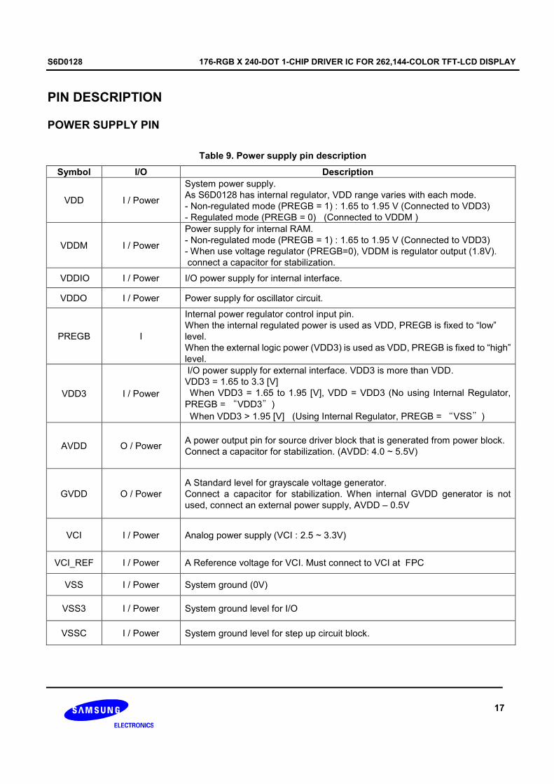
Table 9. Power supply pin description
Symbol I/O Description
VDD I / Power
System power supply.
As S6D0128 has internal regulator, VDD range varies with each mode.
- Non-regulated mode (PREGB = 1) : 1.65 to 1.95 V (Connected to VDD3)
- Regulated mode (PREGB = 0) (Connected to VDDM )
VDDM I / Power
Power supply for internal RAM.
- Non-regulated mode (PREGB = 1) : 1.65 to 1.95 V (Connected to VDD3)
- When use voltage regulator (PREGB=0), VDDM is regulator output (1.8V).
connect a capacitor for stabilization.
VDDIO I / Power I/O power supply for internal interface.
VDDO I / Power Power supply for oscillator circuit.
PREGB I
Internal power regulator control input pin.
When the internal regulated power is used as VDD, PREGB is fixed to “low”
level.
When the external logic power (VDD3) is used as VDD, PREGB is fixed to “high”
level.
VDD3 I / Power
I/O power supply for external interface. VDD3 is more than VDD.
VDD3 = 1.65 to 3.3 [V]
When VDD3 = 1.65 to 1.95 [V], VDD = VDD3 (No using Internal Regulator,
PREGB = “VDD3”)
When VDD3 > 1.95 [V] (Using Internal Regulator, PREGB = “VSS”)
AVDD O / Power A power output pin for source driver block that is generated from power block.
Connect a capacitor for stabilization. (AVDD: 4.0 ~ 5.5V)
GVDD O / Power
A Standard level for grayscale voltage generator.
Connect a capacitor for stabilization. When internal GVDD generator is not
used, connect an external power supply, AVDD – 0.5V
VCI I / Power Analog power supply (VCI : 2.5 ~ 3.3V)
VCI_REF I / Power A Reference voltage for VCI. Must connect to VCI at FPC
VSS I / Power System ground (0V)
VSS3 I / Power System ground level for I/O
VSSC I / Power System ground level for step up circuit block.
176-RGB X 240-DOT 1-CHIP DRIVER IC FOR 262,144-COLOR TFT-LCD DISPLAY S6D0128
18
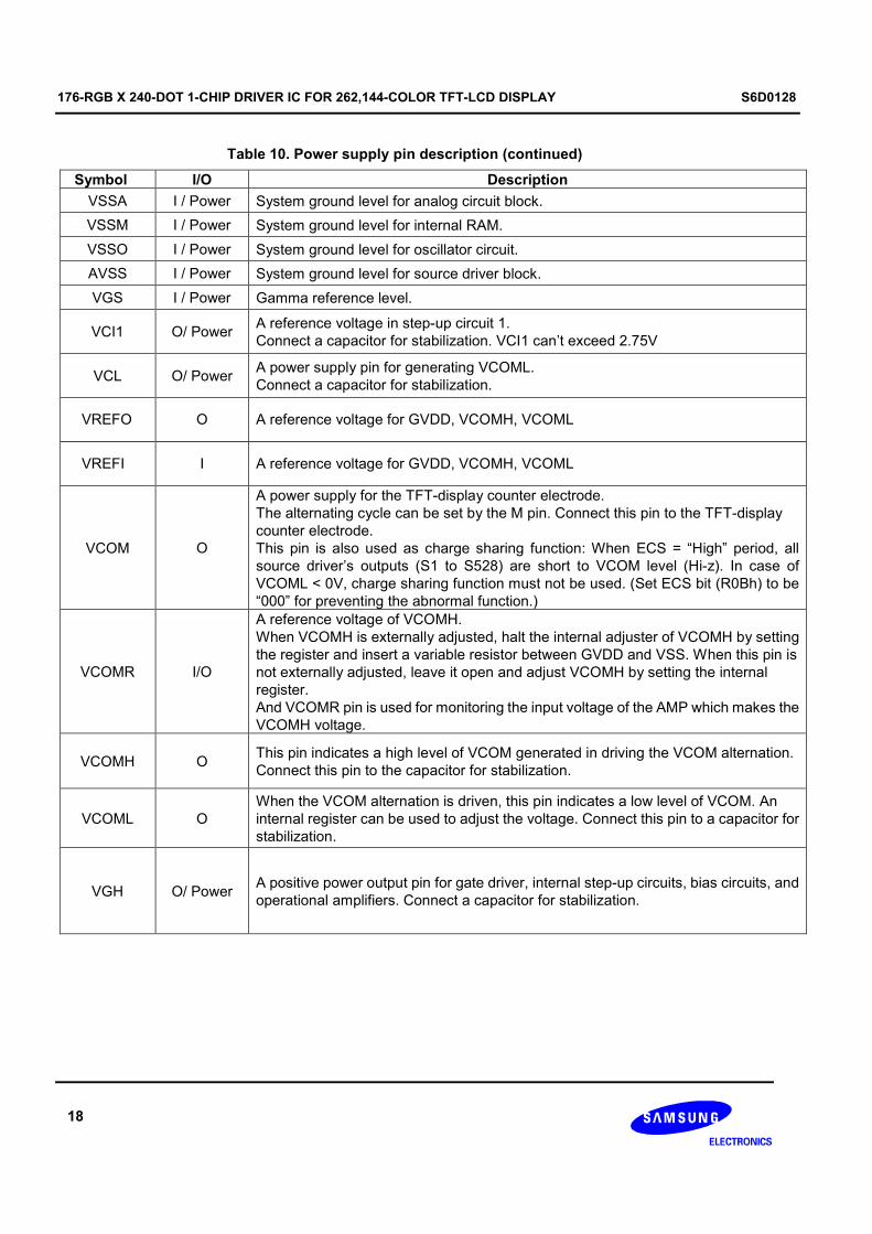
Table 10. Power supply pin description (continued)
Symbol I/O Description
VSSA I / Power System ground level for analog circuit block.
VSSM I / Power System ground level for internal RAM.
VSSO I / Power System ground level for oscillator circuit.
AVSS I / Power System ground level for source driver block.
VGS I / Power Gamma reference level.
VCI1 O/ Power A reference voltage in step-up circuit 1.
Connect a capacitor for stabilization. VCI1 can’t exceed 2.75V
VCL O/ Power A power supply pin for generating VCOML.
Connect a capacitor for stabilization.
VREFO O A reference voltage for GVDD, VCOMH, VCOML
VREFI I A reference voltage for GVDD, VCOMH, VCOML
VCOM O
A power supply for the TFT-display counter electrode.
The alternating cycle can be set by the M pin. Connect this pin to the TFT-display
counter electrode.
This pin is also used as charge sharing function: When ECS = “High” period, all
source driver’s outputs (S1 to S528) are short to VCOM level (Hi-z). In case of
VCOML < 0V, charge sharing function must not be used. (Set ECS bit (R0Bh) to be
“000” for preventing the abnormal function.)
VCOMR I/O
A reference voltage of VCOMH.
When VCOMH is externally adjusted, halt the internal adjuster of VCOMH by setting
the register and insert a variable resistor between GVDD and VSS. When this pin is
not externally adjusted, leave it open and adjust VCOMH by setting the internal
register.
And VCOMR pin is used for monitoring the input voltage of the AMP which makes the
VCOMH voltage.
VCOMH O This pin indicates a high level of VCOM generated in driving the VCOM alternation.
Connect this pin to the capacitor for stabilization.
VCOML O
When the VCOM alternation is driven, this pin indicates a low level of VCOM. An
internal register can be used to adjust the voltage. Connect this pin to a capacitor for
stabilization.
VGH O/ Power A positive power output pin for gate driver, internal step-up circuits, bias circuits, and
operational amplifiers. Connect a capacitor for stabilization.
S6D0128 176-RGB X 240-DOT 1-CHIP DRIVER IC FOR 262,144-COLOR TFT-LCD DISPLAY
19
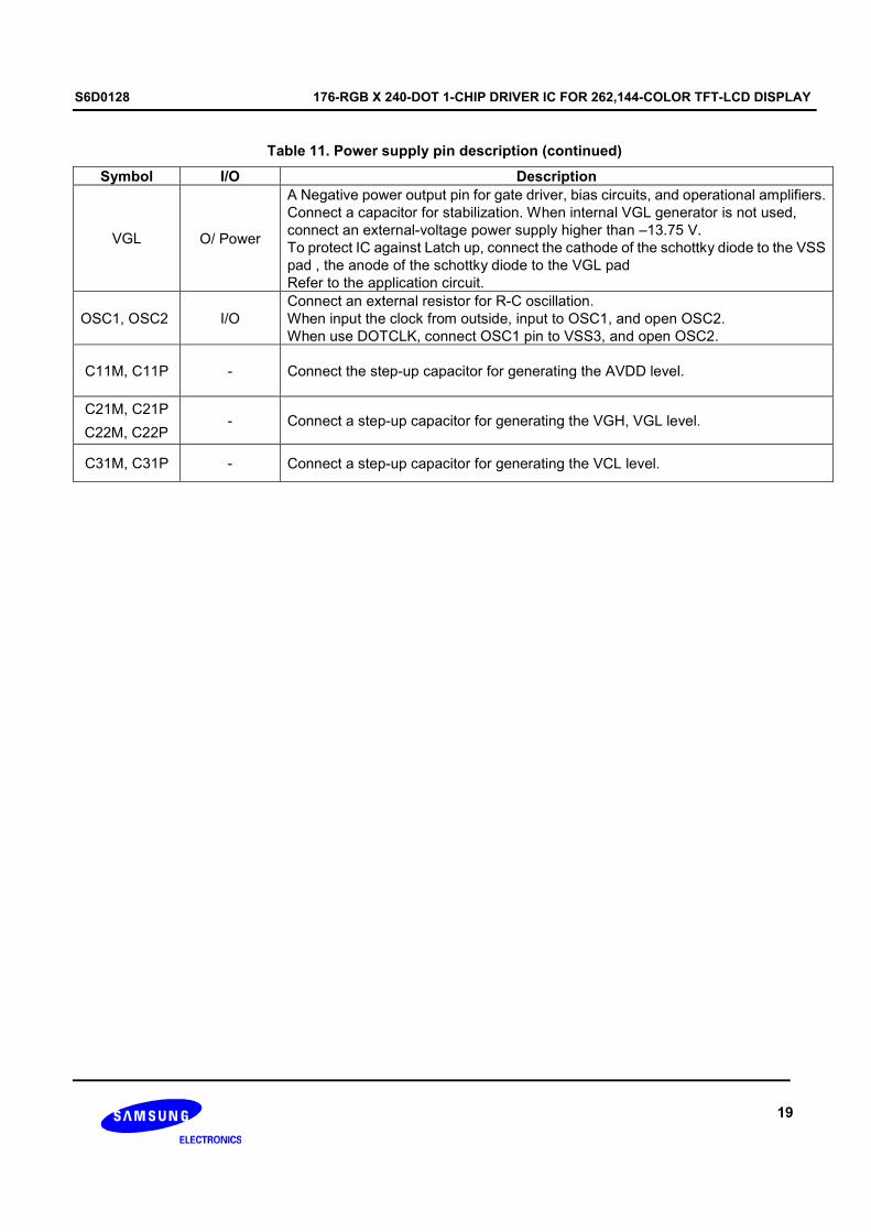
Table 11. Power supply pin description (continued)
Symbol I/O Description
VGL O/ Power
A Negative power output pin for gate driver, bias circuits, and operational amplifiers.
Connect a capacitor for stabilization. When internal VGL generator is not used,
connect an external-voltage power supply higher than –13.75 V.
To protect IC against Latch up, connect the cathode of the schottky diode to the VSS
pad , the anode of the schottky diode to the VGL pad
Refer to the application circuit.
OSC1, OSC2 I/O
Connect an external resistor for R-C oscillation.
When input the clock from outside, input to OSC1, and open OSC2.
When use DOTCLK, connect OSC1 pin to VSS3, and open OSC2.
C11M, C11P - Connect the step-up capacitor for generating the AVDD level.
C21M, C21P
C22M, C22P - Connect a step-up capacitor for generating the VGH, VGL level.
C31M, C31P - Connect a step-up capacitor for generating the VCL level.

176-RGB X 240-DOT 1-CHIP DRIVER IC FOR 262,144-COLOR TFT-LCD DISPLAY S6D0128
20
SYSTEM/RGB INTERFACE PIN
Table 12. System interface pin description
Symbol I/O Description
Selects the MPU interface mode:
IM3 IM2 IM1 IM0/ID MPU interface mode DB PIN assign
VSS VSS VSS VSS 68-system 16-bit bus interface DB17-10, DB8-1
VSS VSS VSS VDD3 68-system 8bit bus interface DB17-10
VSS VSS VDD3 VSS 80-system 16bit bus interface DB17-10, DB8-1
VSS VSS VDD3 VDD3 80-system 8bit bus interface DB17-10
VSS VDD3 VSS ID Serial peripheral interface (SPI) SDI / SDO
VSS VDD3 VDD3 * Non-selecting -
VDD3 VSS VSS VSS 68-system 18-bit bus interface DB17-0
VDD3 VSS VSS VDD3 68-system 9bit bus interface DB17-9
VDD3 VSS VDD3 VSS 80-system 18bit bus interface DB17-0
VDD3 VSS VDD3 VDD3 80-system 9bit bus interface DB17-9
VDD3 VDD3 * * Non-selecting -
IM3-1,
IM0/ID I
1) When a SPI mode is selected, the IM0 pin is used as ID setting bit for a device code.
2) In RGB interface mode, the IM3-0 pins must select SPI mode.
CSB I
Chip select signal input pin.
Low: S6D0128 is selected and can be accessed
High: S6D0128 is not selected and cannot be accessed
RS I
Register select pin.
Low: Index/status, High: Control
Must be fixed at VSS level when not used.
IM3 IM2 IM1 Pin
function MPU type Pin description
* VSS VSS RW 68-system Read/Write operation selection pin.
Low: Write , High: Read
* VSS VDD3 WRB 80-system Write strobe signal input pin.
Data is fetched at the rising edge.
RW_WRB/
SCL I
VSS VDD3 VSS SCL serial peripheral
interface (SPI)
the synchronous clock signal input
pin
IM3 IM2 IM1 Pin
function MPU type Pin description
* VSS VSS E 68-system Read/Write operation enable pin.
* VSS VDD3 RDB 80-system Read strobe signal input pin.
Read out data at the low level.
E_RDB I
When SPI mode is selected, fix this pin at VSS level.
SDI I
For a serial peripheral interface (SPI), input data is fetched at the rising edge of the SCL
signal.
Fix SDI to the VDD3 or VSS level if the pin is not in use.
SDO O
For a serial peripheral interface (SPI), serves as the serial data output pin (SDO).
Successive bits are output at the falling edge of the SCL signal
SDO must be opened when not used
S6D0128 176-RGB X 240-DOT 1-CHIP DRIVER IC FOR 262,144-COLOR TFT-LCD DISPLAY
21
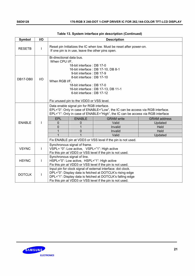
Table 13. System interface pin description (Continued)
Symbol I/O Description
RESETB I Reset pin Initializes the IC when low. Must be reset after power-on.
If one pin is in use, leave the other pins open.
DB17-DB0 I/O
Bi-directional data bus.
When CPU I/F,
18-bit interface : DB 17-0
16-bit interface : DB 17-10, DB 8-1
9-bit interface : DB 17-9
8-bit interface : DB 17-10
When RGB I/F,
18-bit interface : DB 17-0
16-bit interface : DB 17-13, DB 11-1
6-bit interface : DB 17-12
Fix unused pin to the VDD3 or VSS level.
Data enable signal pin for RGB interface.
EPL=”0”: Only in case of ENABLE=”Low”, the IC can be access via RGB interface.
EPL=”1”: Only in case of ENABLE=”High”, the IC can be access via RGB interface
EPL ENABLE GRAM write GRAM address
0 0 Valid Updated
0 1 Invalid Held
1 0 Invalid Held
1 1 Valid Updated
ENABLE I
Fix ENABLE pin at VDD3 or VSS level if the pin is not used.
VSYNC I
Synchronous signal of frame.
VSPL= “0”: Low active, VSPL=”1”: High active
Fix this pin at VDD3 or VSS level if the pin is not used.
HSYNC I
Synchronous signal of line.
HSPL=”0”: Low active, HSPL=”1”: High active
Fix this pin at VDD3 or VSS level if the pin is not used.
DOTCLK I
Input pin for clock signal of external interface: dot clock.
DPL=”0”: Display data is fetched at DOTCLK’s rising edge
DPL=”1”: Display data is fetched at DOTCLK’s falling edge
Fix this pin at VDD3 or VSS level if the pin is not used.

176-RGB X 240-DOT 1-CHIP DRIVER IC FOR 262,144-COLOR TFT-LCD DISPLAY S6D0128
22
DISPLAY PIN
Table 14. Display pin description
Symbol I/O Description
S1 – S528 O
Source driver output pins.
The SS bit can change the shift direction of the source signal.
For example, if SS = 0, gray data of <S1/S2/S3> is read from RAM address 0000h.
If SS = 1, contents of is RAM address 0000h is out from <S526/S527/S528>.
S1, S4, S7, ... S(3n-1) : display Red (R) (BGR = 0)
S2, S5, S8, ... S(3n-2) : display Green (G) (BGR = 0)
S3, S6, S9, ... S(3n) : display Blue (B) (BGR = 0)
G1 – G240 O
Gate driver output pins.
The output of driving circuit is whether VGH or VGL.
VGH : gate-ON level
VGL : gate-OFF level
MISCELLANEOUS PIN
Table 15. Oscillator and internal power regulator pin description
Symbol I/O Description
TAD9-TAD0/
TSI0/TSI1
TEST/
TEST_MUX/
TEST_GRAY
I Input pin for test. In normal operation, connect this pin to VSS3.
FUSE_EN I Input pin for test. In normal operation, connect this pin to VDD3.
VCIR I Input pin for test. In normal operation, connect this pin to VCI.
ATEST I Input pin for test. In normal operation, open this pin .
DISPTMG/
PREC/ M/ CL1/
ECS/ FLM/
/ TSO
O Output pin for test. In normal operation, leave this pin open.
DUMMY - Dummy pin. Open or connect VSS3.
GMON O Monitoring grayscale voltage level - V0P/N, V63P/N - monitoring pin.
Must be opened when not used
VDD3O,
VSS3O -
Output dummy pin for mode setting. Connect these pin to adjacent logic input pin.
Must be opened when not used.
CONTACT1,
CONTACT2 -
Pass-through pin.
Identical pins at input and output part that is connected without any circuitry.

S6D0128 176-RGB X 240-DOT 1-CHIP DRIVER IC FOR 262,144-COLOR TFT-LCD DISPLAY
23
FUNCTIONAL DESCRIPTION
SYSTEM INTERFACE
The S6D0128 has nine high-speed system interfaces: an 80-system 18-/16-/9-/8-bit bus, a 68-system
18-/16-/9-/8-bit bus, and a serial interface (SPI: Serial Peripheral Interface). The IM3-0 pins select the interface
mode.
The S6D0128 has three 18-bit registers: an index register (IR), a write data register (WDR), and a read data register
(RDR). The IR stores index information for control register and GRAM. The WDR temporarily stores data to be
written into control register and GRAM. The RDR temporarily stores data read from GRAM. Data written into the
GRAM from MPU is initially written to the WDR and then written to the GRAM automatically. Data is read through the
RDR when reading from the GRAM, and the first read data is invalid and the second and the following data are valid.
Execution time for instruction, except oscillation start, is 0-clock cycle so that instructions can be written in
succession.
Table 16. Register Selection (18-/16-/9-/8- Parallel Interface)
SYSTEM RW_WRB E_RDB RS Operations
0 1 0 Write index to IR
1 1 0 Read internal status
0 1 1 Write to control register and GRAM through WDR 68
1 1 1 Read from GRAM through RDR
0 1 0 Write index to IR
1 0 0 Read internal status
0 1 1 Write to control register and GRAM through WDR 80
1 0 1 Read from GRAM through RDR
Table 17. CSB signal (GRAM update control)
CSB Operation
0 Data is written to GRAM, GRAM address is updated
1 Data is not written to GRAM, GRAM address is not updated
Table 18. Register Selection (Serial Peripheral Interface)
R/W bit RS bit Operation
0 0 Write index to IR
1 0 Read internal status
0 1 Write data to control register and GRAM through WDR
1 1 Read data from GRAM through RDR
176-RGB X 240-DOT 1-CHIP DRIVER IC FOR 262,144-COLOR TFT-LCD DISPLAY S6D0128
24
EXTERNAL INTERFACE (RGB-I/F, VSYNC-I/F)
The S6D0128 incorporates RGB and VSYNC interface as external interface for motion picture display.
When the RGB interface is selected, the synchronization signals (VSYNC, HSYNC, and DOTCLK) are available for
display. The RGB data for display (DB17-0) are written according to enable signal (ENABLE) and data valid signal
(VLD) in synchronization with VSYNC, HSYNC, and DOTCLK signal. This allows flicker-free updating of the screen.
When the VSYNC interface is selected, internal operation is normally synchronized with internal clock except
operation related to frame synchronization: It is synchronized with the VSYNC signal. The data for display are
written to GRAM via conventional system interface. There are some limitations on the timing and methods for writing
to GRAM in VSYNC interface. See the section on the EXTERNAL DISPLAY INTERFACE.
ADDRESS COUNTER (AC)
The address counter (AC) assigns address to GRAM. When an address-set-instruction is written to the IR, the
address information is sent from IR to AC. After writing to the GRAM, the address value of AC is automatically
increased/ decreased by 1 according to ID1-0 bit of control register. After reading data from GRAM, the AC is not
updated. A window address function allows data to be written only to a window area specified by GRAM.
GRAPHICS RAM (GRAM)
The graphics RAM (GRAM) has 18-bits/pixel and stores the bit-pattern data for 176-RGB x 240-dot display.
GRAYSCALE VOLTAGE GENERATOR
The grayscale voltage circuit generates a certain voltage level that is specified by the grayscale ϒ-adjusting register
for LCD driver circuit. By use of the generator, 262,144 colors can be displayed at the same time. For details, see the
GAMMA-ADJUSTING REGISTER section.
TIMING GENERATOR
The timing generator generates timing signals for the operation of internal circuits such as GRAM.
The GRAM read timing for display and the internal operation timing for MPU access is generated separately to avoid
interference with one another. Several important timing signals can be monitored via signal monitoring pin (M, FLM,
CL1, ECS, DISPTMG, PREC).
OSCILLATION CIRCUIT (OSC)
The S6D0128 can provide R-C oscillation simply through the addition of an external oscillation-resistor between the
OSC1 and OSC2 pin. The appropriate oscillation frequency for operating voltage, display size, and frame frequency
can be obtained by adjusting the external-resistor value. Clock pulse can also be supplied externally. Since R-C
oscillation stops during the standby mode, current consumption can be reduced. For details, see the OSCILLATION
CIRCUIT section.

S6D0128 176-RGB X 240-DOT 1-CHIP DRIVER IC FOR 262,144-COLOR TFT-LCD DISPLAY
25
SOURCE DRIVER CIRCUIT
The liquid crystal display source driver circuit consists of 528 drivers (S1 to S528).
Display pattern data is latched when 528-channel data has arrived. The latched data then enables the source
drivers to generate drive waveform outputs. The SS bit can change the shift direction of 528-channel data by
selecting an appropriate direction for the device-mounted configuration.
GATE DRIVER CIRCUIT
The liquid crystal display gate driver circuit consists of 240 gate drivers (G1 to G240).
The VGH or VGL level is output by the signal from the gate control circuit.

176-RGB X 240-DOT 1-CHIP DRIVER IC FOR 262,144-COLOR TFT-LCD DISPLAY S6D0128
26
SYSTEM/RGB INTERFACE AND GRAM ADDRESS SETTING
GRAM ADDRESS SETTING (SS=”0”)
When SS bit is 0 (source output shift direction: right) and BGR bit is 0 (RGB sequence: right) that can be set in R01h,
R03h register, GRAM address is set as follows:
Table 19. GRAM address (SS=”0”)
S1
S2
S3
S4
S5
S6
S7
S8
S9
S10
S11
S12
………
S517
S518
S519
S520
S521
S522
S523
S524
S525
S526
S527
S528
DB DB DB DB DB DB DB DB DB DB DB DB DB DB DB DB
17 0 17 0 17 0 17 0 17 0 17 0 17 0 17 0
G1 G240 ………G2 G239 ………G3 G238 ………G4 G237 ………G5 G236 ………G6 G235 ………G7 G234 ………G8 G233 ………G9 G232 ………G10 G231 ………G11 G230 ………G12 G229 ………G13 G228 ………G14 G227 ………G15 G226 ………G16 G225 ………G17 G224 ………G18 G223 ………G19 G222 ………G20 G221 ………
G233 G8 ………G234 G7 ………G235 G6 ………G236 G5 ………G237 G4 ………G238 G3 ………G239 G2 ………G240 G1 ………
S/G Output
GS=0 GS=1 …… ……
"0000"H "0001"H "0002"H "0003"H
"0100"H "0101"H "0102"H "0103"H
"0200"H "0201"H "0202"H "0203"H
"0300"H "0301"H "0302"H "0303"H
"0400"H "0401"H "0402"H "0403"H
"0500"H "0501"H "0502"H "0503"H
"0600"H "0601"H "0602"H "0603"H
"0700"H "0701"H "0702"H "0703"H
"0800"H "0801"H "0802"H "0803"H
"0900"H "0901"H "0902"H "0903"H
"0A00"H "0A01"H "0A02"H "0A03"H
"0B00"H "0B01"H "0B02"H "0B03"H
"0C00"H "0C01"H "0C02"H "0C03"H
"0D00"H "0D01"H "0D02"H "0D03"H
"0E00"H "0E01"H "0E02"H "0E03"H
"0F00"H "0F01"H "0F02"H "0F03"H
"1000"H "1001"H "1002"H "1003"H
"1100"H "1101"H "1102"H "1103"H
"1200"H "1201"H "1202"H "1203"H
……
……
……
"1300"H
……
……
……
"1301"H "1302"H "1303"H
…… ……
"E800"H "E801"H "E801"H "E803"H
"E900"H "E901"H "E902"H "E903"H
"EA00"H "EA01"H "EA02"H "EA03"H
"EB00"H "EB01"H "EB02"H "EB03"H
"EC00"H "EC01"H "EC02"H "EC03"H
"ED00"H "ED01"H "ED02"H "ED03"H
"EE00"H "EE01"H "EE02"H "EE03"H
"EF00"H "EF01"H "EF02"H "EF03"H
…… …… …… ……
"00AC"H "00AD"H "00AE"H "00AF"H
"01AC"H "01AD"H "01AE"H "01AF"H
"02AC"H "02AD"H "02AE"H "02AF"H
"03AC"H "03AD"H "03AE"H "03AF"H
"04AC"H "04AD"H "04AE"H "04AF"H
"05AC"H "05AD"H "05AE"H "05AF"H
"06AC"H "06AD"H "06AE"H "06AF"H
"07AC"H "07AD"H "07AE"H "07AF"H
"08AC"H "08AD"H "08AE"H "08AF"H
"09AC"H "09AD"H "09AE"H "09AF"H
"0AAC"H "0AAD"H "0AAE"H "0AAF"H
"0BAC"H "0BAD"H "0BAE"H "0BAF"H
"0CAC"H "0CAD"H "0CAE"H "0CAF"H
"0DAC"H "0DAD"H "0DAE"H "0DAF"H
"0EAC"H "0EAD"H "0EAE"H "0EAF"H
"0FAC"H "0FAD"H "0FAE"H "0FAF"H
"10AC"H "10AD"H "10AE"H "10AF"H
"11AC"H "11AD"H "11AE"H "11AF"H
"12AC"H "12AD"H "12AE"H "12AF"H
"13AC"H "13AD"H "13AE"H "13AF"H
……
……
……
……
"E8AC"H "E8AD"H "E8AE"H "E8AF"H
"E9AC"H "E9AD"H "E9AE"H "E9AF"H
"EAAC"H "EAAD"H "EAAE"H "EAAF"H
"EBAC"H "EBAD"H "EBAE"H "EBAF"H
"ECAC"H "ECAD"H "ECAE"H "ECAF"H
"EDAC"H "EDAD"H "EDAE"H "EDAF"H
"EEAC"H "EEAD"H "EEAE"H "EEAF"H
"EFAC"H "EFAD"H "EFAE"H "EFAF"H

S6D0128 176-RGB X 240-DOT 1-CHIP DRIVER IC FOR 262,144-COLOR TFT-LCD DISPLAY
27
Data fetch from GRAM for display when SS=0 is shown in the following figure.
SYSTEM INTERFACE
68/80-system 18-bit interface
DB
17
DB
16
DB
15
DB
14
DB
13
DB
12
DB
11
DB
10
DB
9
DB
8
DB
7
DB
6
DB
5
DB
4
DB
3
DB
2
DB
1
DB
0INPUT DATA
R5 R4 R3 R2 R1 R0
S (3n + 1)
G5 G4 G3 G2 G1 G0
S (3n + 2)
B5 B4 B3 B2 B1 B0
S (3n + 3)
RGB Arrangement
Output
Note: n= lower 8 bits of address (0 to 175)
68/80-system 16-bit interface (TRI=0, DFM1-0=00)
DB
17
DB
16
DB
15
DB
14
DB
13
DB
12
DB
11
DB
10
DB
8
DB
7
DB
6
DB
5
DB
4
DB
3
DB
2
DB
1INPUT DATA
R5 R4 R3 R2 R1 R0
S (3n + 1)
G5 G4 G3 G2 G1 G0
S (3n + 2)
B5 B4 B3 B2 B1 B0
S (3n + 3)
RGB Arrangement
Output
Note: n= lower 8 bits of address (0 to 175)
68/80-system 9-bit interface
DB
17
DB
16
DB
15
DB
14
DB
13
DB
12
DB
11
DB
10
DB
9INPUT DATA
R5 R4 R3 R2 R1 R0
S (3n + 1)
G5 G4 G3 G2 G1 G0
S (3n + 2)
B5 B4 B3 B2 B1 B0
S (3n + 3)
RGB Arrangement
Output
Note: n= lower 8 bits of address (0 to 175)
1st Transmission
DB
17
DB
16
DB
15
DB
14
DB
13
DB
12
DB
11
DB
10
DB
9
2nd Transmission

176-RGB X 240-DOT 1-CHIP DRIVER IC FOR 262,144-COLOR TFT-LCD DISPLAY S6D0128
28
68/80-system 8-bit interface (TRI=0, DFM1-0=00)
DB
17
DB
16
DB
15
DB
14
DB
13
DB
12
DB
11
DB
10
DB
17
DB
16
DB
15
DB
14
DB
13
DB
12
DB
11
DB
10INPUT DATA
R5 R4 R3 R2 R1 R0
S (3n + 1)
G5 G4 G3 G2 G1 G0
S (3n + 2)
B5 B4 B3 B2 B1 B0
S (3n + 3)
RGB Arrangement
Output
Note: n= lower 8 bits of address (0 to 175)
1st Transmission 2nd Transmission
80-system 16-bit interface (TRI=1, DFM1-0=10)
DB
17
DB
16
DB
15
DB
14
DB
13
DB
12
DB
11
DB
10
DB
8INPUT DATA
R5 R4 R3 R2 R1 R0
S (3n + 1)
G5 G4 G3 G2 G1 G0
S (3n + 2)
B5 B4 B3 B2 B1 B0
S (3n + 3)
RGB Arrangement
Output
Note: n= lower 8 bits of address (0 to 175)
1st Transmission
DB
7
DB
6
DB
5
DB
4
DB
3
DB
2
DB
1
DB
17
DB
16
2nd
Transmission
80-system 16-bit interface (TRI=1, DFM1-0=11)
DB
2
DB
1
DB
17
DB
16
DB
15
DB
14
DB
13
DB
12
DB
11INPUT DATA
R5 R4 R3 R2 R1 R0
S (3n + 1)
G5 G4 G3 G2 G1 G0
S (3n + 2)
B5 B4 B3 B2 B1 B0
S (3n + 3)
RGB Arrangement
Output
Note: n= lower 8 bits of address (0 to 175)
1st
Transmission
DB
10
DB
8
DB
7
DB
6
DB
5
DB
4
DB
3
DB
2
DB
1
2nd Transmission

S6D0128 176-RGB X 240-DOT 1-CHIP DRIVER IC FOR 262,144-COLOR TFT-LCD DISPLAY
29
80-system 8-bit interface (TRI=1, DFM1-0=10)
DB
17
DB
16
DB
15
DB
14
DB
13
DB
12INPUT DATA
R5 R4 R3 R2 R1 R0
S (3n + 1)
G5 G4 G3 G2 G1 G0
S (3n + 2)
B5 B4 B3 B2 B1 B0
S (3n + 3)
RGB Arrangement
Output
Note: n= lower 8 bits of address (0 to 175)
1st Transmission 2nd Transmission 3rd Transmission
DB
17
DB
16
DB
15
DB
14
DB
13
DB
12
DB
17
DB
16
DB
15
DB
14
DB
13
DB
12
80-system 8-bit interface (TRI=1, DFM1-0=11)
DB
17
DB
16
DB
15
DB
14
DB
13
DB
12INPUT DATA
R5 R4 R3 R2 R1 R0
S (3n + 1)
G5 G4 G3 G2 G1 G0
S (3n + 2)
B5 B4 B3 B2 B1 B0
S (3n + 3)
RGB Arrangement
Output
Note: n= lower 8 bits of address (0 to 175)
1st Transmission 2nd Transmission 3rd Transmission
DB
17
DB
16
DB
15
DB
14
DB
13
DB
12
DB
17
DB
16
DB
15
DB
14
DB
13
DB
12

176-RGB X 240-DOT 1-CHIP DRIVER IC FOR 262,144-COLOR TFT-LCD DISPLAY S6D0128
30
RGB INTERFACE
18-bit RGB interface
DB
17 16 15 14 13 12 11 10 9 8 7 6 5 4 3 2 1 0INPUT DATA
R5 R4 R3 R2 R1 R0
S (3n + 1)
G5 G4 G3 G2 G1 G0
S (3n + 2)
B5 B4 B3 B2 B1 B0
S (3n + 3)
RGB Arrangement
Output
Note: n= lower 8 bits of address (0 to 175)
DB DB DB DB DB DB DB DB DB DB DB DB DB DB DB DB DB
16-bit RGB interface
DB
17
DB
16
DB
15
DB
14
DB
13
DB
9
DB
11
DB
10
DB
8
DB
7
DB
6
DB
5
DB
4
DB
3
DB
2
DB
1INPUT DATA
R5 R4 R3 R2 R1 R0
S (3n + 1)
G5 G4 G3 G2 G1 G0
S (3n + 2)
B5 B4 B3 B2 B1 B0
S (3n + 3)
RGB Arrangement
Output
Note: n= lower 8 bits of address (0 to 175)
6-bit RGB interface
DB
17
DB
16
DB
15
DB
14
DB
13
DB
12INPUT DATA
R5 R4 R3 R2 R1 R0
S (3n + 1)
G5 G4 G3 G2 G1 G0
S (3n + 2)
B5 B4 B3 B2 B1 B0
S (3n + 3)
RGB Arrangement
Output
Note: n= lower 8 bits of address (0 to 175)
1st Transmission 2nd Transmission 3rd Transmission
DB
17
DB
16
DB
15
DB
14
DB
13
DB
12
DB
17
DB
16
DB
15
DB
14
DB
13
DB
12
S6D0128 176-RGB X 240-DOT 1-CHIP DRIVER IC FOR 262,144-COLOR TFT-LCD DISPLAY
31
GRAM ADDRESS SETTING (SS=”1”)
When SS bit is 1 (source output shift direction: reversed) and BGR bit is 1 (RGB sequence: reversed) that can be set
in R01h, R03h register, GRAM address is set as follows:
Table 20. GRAM address (SS=”1”)
S1
S2
S3
S4
S5
S6
S7
S8
S9
S10
S11
S12
………
S517
S518
S519
S520
S521
S522
S523
S524
S525
S526
S527
S528
DB DB DB DB DB DB DB DB DB DB DB DB DB DB DB DB
0 17 0 17 0 17 0 17 0 17 0 17 0 17 0 17
G1 G240 ………G2 G239 ………G3 G238 ………G4 G237 ………G5 G236 ………G6 G235 ………G7 G234 ………G8 G233 ………G9 G232 ………G10 G231 ………G11 G230 ………G12 G229 ………G13 G228 ………G14 G227 ………G15 G226 ………G16 G225 ………G17 G224 ………G18 G223 ………G19 G222 ………G20 G221 ………
G233 G8 ………G234 G7 ………G235 G6 ………G236 G5 ………G237 G4 ………G238 G3 ………G239 G2 ………G240 G1 ………
S/G Output
GS=0 GS=1 …… …… …… …… …… …… …… ……
"00AF"H "00AE"H "00AD"H "00AC"H "0003"H "0002"H "0001"H "0000"H
"01AF"H "01AE"H "01AD"H "01AC"H "0103"H "0102"H "0101"H "0100"H
"02AF"H "02AE"H "02AD"H "02AC"H "0203"H "0202"H "0201"H "0200"H
"03AF"H "03AE"H "03AD"H "03AC"H "0303"H "0302"H "0301"H "0300"H
"04AF"H "04AE"H "04AD"H "04AC"H "0403"H "0402"H "0401"H "0400"H
"05AF"H "05AE"H "05AD"H "05AC"H "0503"H "0502"H "0501"H "0500"H
"06AF"H "06AE"H "06AD"H "06AC"H "0603"H "0602"H "0601"H "0600"H
"07AF"H "07AE"H "07AD"H "07AC"H "0703"H "0702"H "0701"H "0700"H
"08AF"H "08AE"H "08AD"H "08AC"H "0803"H "0802"H "0801"H "0800"H
"09AF"H "09AE"H "09AD"H "09AC"H "0903"H "0902"H "0901"H "0900"H
"0AAF"H "0AAE"H "0AAD"H "0AAC"H "0A03"H "0A02"H "0A01"H "0A00"H
"0BAF"H "0BAE"H "0BAD"H "0BAC"H "0B03"H "0B02"H "0B01"H "0B00"H
"0CAF"H "0CAE"H "0CAD"H "0CAC"H "0C03"H "0C02"H "0C01"H "0C00"H
"0DAF"H "0DAE"H "0DAD"H "0DAC"H "0D03"H "0D02"H "0D01"H "0D00"H
"0EAF"H "0EAE"H "0EAD"H "0EAC"H "0E03"H "0E02"H "0E01"H "0E00"H
"0FAF"H "0FAE"H "0FAD"H "0FAC"H "0F03"H "0F02"H "0F01"H "0F00"H
"10AF"H "10AE"H "10AD"H "10AC"H "1003"H "1002"H "1001"H "1000"H
"11AF"H "11AE"H "11AD"H "11AC"H "1103"H "1102"H "1101"H "1100"H
"12AF"H "12AE"H "12AD"H "12AC"H "1203"H "1202"H "1201"H "1200"H
"1302"H "1301"H "1300"H"13AF"H "13AE"H "13AD"H "13AC"H
……
……
……
"1303"H
……
……
……
……
……
……
"E8AE"H "E8AD"H "E8AC"H "E803"H "E801"H "E801"H
……
"E800"H
"E9AF"H "E9AE"H "E9AD"H "E9AC"H "E903"H "E902"H "E901"H "E900"H
"E8AF"H
"EAAF"H "EAAE"H "EAAD"H "EAAC"H "EA03"H "EA02"H "EA01"H "EA00"H
"EBAF"H "EBAE"H "EBAD"H "EBAC"H "EB03"H "EB02"H "EB01"H "EB00"H
"ECAF"H "ECAE"H "ECAD"H "ECAC"H "EC03"H "EC02"H "EC01"H "EC00"H
"EDAF"H "EDAE"H "EDAD"H "EDAC"H "ED03"H "ED02"H "ED01"H "ED00"H
"EEAF"H "EEAE"H "EEAD"H "EEAC"H "EE03"H "EE02"H "EE01"H "EE00"H
"EFAF"H "EFAE"H "EFAD"H "EFAC"H "EF03"H "EF02"H "EF01"H "EF00"H

176-RGB X 240-DOT 1-CHIP DRIVER IC FOR 262,144-COLOR TFT-LCD DISPLAY S6D0128
32
Data fetch from GRAM for display when SS=1, BGR = 1 is shown in the following figure.
SYSTEM INTERFACE
68/80-system 18-bit interface
DB
17
DB
16
DB
15
DB
14
DB
13
DB
12
DB
11
DB
10
DB
9
DB
8
DB
7
DB
6
DB
5
DB
4
DB
3
DB
2
DB
1
DB
0INPUT DATA
R5 R4 R3 R2 R1 R0
S (528-3n)
G5 G4 G3 G2 G1 G0
S (527-3n)
B5 B4 B3 B2 B1 B0
S (526-3n)
RGB Arrangement
Output
Note: n= lower 8 bits of address (0 to 175)
68/80-system 16-bit interface (TRI=0, DFM1-0=00)
DB
17
DB
16
DB
15
DB
14
DB
13
DB
12
DB
11
DB
10
DB
8
DB
7
DB
6
DB
5
DB
4
DB
3
DB
2
DB
1INPUT DATA
R5 R4 R3 R2 R1 R0 G5 G4 G3 G2 G1 G0 B5 B4 B3 B2 B1 B0RGB Arrangement
Output
Note: n= lower 8 bits of address (0 to 175)
S (528-3n) S (527-3n) S (526-3n)
68/80-system 9-bit interface
DB
17
DB
16
DB
15
DB
14
DB
13
DB
12
DB
11
DB
10
DB
9INPUT DATA
R5 R4 R3 R2 R1 R0 G5 G4 G3 G2 G1 G0 B5 B4 B3 B2 B1 B0RGB Arrangement
Output
Note: n= lower 8 bits of address (0 to 175)
1st Transmission
DB
17
DB
16
DB
15
DB
14
DB
13
DB
12
DB
11
DB
10
DB
9
2nd Transmission
S (528-3n) S (527-3n) S (526-3n)

S6D0128 176-RGB X 240-DOT 1-CHIP DRIVER IC FOR 262,144-COLOR TFT-LCD DISPLAY
33
68/80-system 8-bit interface (TRI=0, DFM1-0=00)
DB
17
DB
16
DB
15
DB
14
DB
13
DB
12
DB
11
DB
10
DB
17
DB
16
DB
15
DB
14
DB
13
DB
12
DB
11
DB
10INPUT DATA
R5 R4 R3 R2 R1 R0 G5 G4 G3 G2 G1 G0 B5 B4 B3 B2 B1 B0RGB Arrangement
Output
Note: n= lower 8 bits of address (0 to 175)
1st Transmission 2nd Transmission
S (528-3n) S (527-3n) S (526-3n)
80-system 16-bit interface (TRI=1, DFM1-0=10)
DB
17
DB
16
DB
15
DB
14
DB
13
DB
12
DB
11
DB
10
DB
8INPUT DATA
R5 R4 R3 R2 R1 R0
S(528-3n)
G5 G4 G3 G2 G1 G0
S(527-3n)
B5 B4 B3 B2 B1 B0
S(526-3n)
RGB Arrangement
Output
Note: n= lower 8 bits of address (0 to 175)
1st Transmission
DB
7
DB
6
DB
5
DB
4
DB
3
DB
2
DB
1
DB
17
DB
16
2nd
Transmission
80-system 16-bit interface (TRI=1, DFM1-0=11)
DB
2
DB
1
DB
17
DB
16
DB
15
DB
14
DB
13
DB
12
DB
11INPUT DATA
R5 R4 R3 R2 R1 R0
S(528-3n)
G5 G4 G3 G2 G1 G0
S(527-3n)
B5 B4 B3 B2 B1 B0
S(526-3n)
RGB Arrangement
Output
Note: n= lower 8 bits of address (0 to 175)
1st
Transmission
DB
10
DB
8
DB
7
DB
6
DB
5
DB
4
DB
3
DB
2
DB
1
2nd Transmission
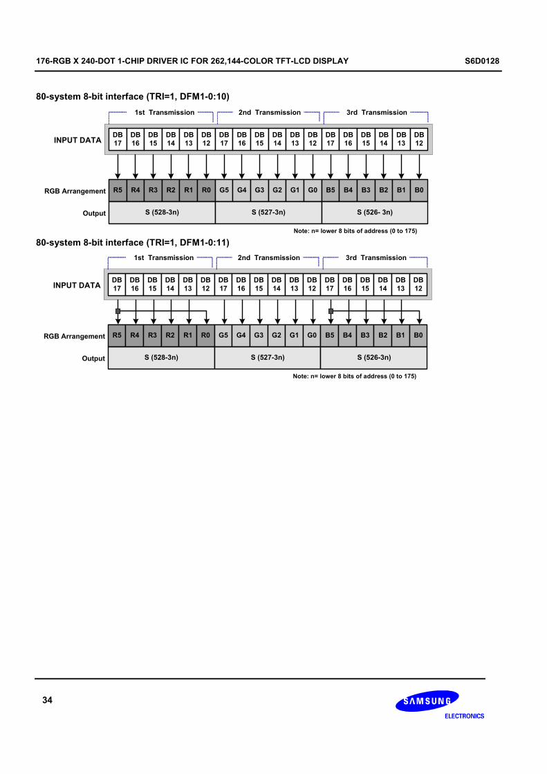
176-RGB X 240-DOT 1-CHIP DRIVER IC FOR 262,144-COLOR TFT-LCD DISPLAY S6D0128
34
80-system 8-bit interface (TRI=1, DFM1-0:10)
DB
17
DB
16
DB
15
DB
14
DB
13
DB
12INPUT DATA
R5 R4 R3 R2 R1 R0
S (528-3n)
G5 G4 G3 G2 G1 G0
S (527-3n)
B5 B4 B3 B2 B1 B0
S (526- 3n)
RGB Arrangement
Output
Note: n= lower 8 bits of address (0 to 175)
1st Transmission 2nd Transmission 3rd Transmission
DB
17
DB
16
DB
15
DB
14
DB
13
DB
12
DB
17
DB
16
DB
15
DB
14
DB
13
DB
12
80-system 8-bit interface (TRI=1, DFM1-0:11)
DB
17
DB
16
DB
15
DB
14
DB
13
DB
12INPUT DATA
R5 R4 R3 R2 R1 R0
S (528-3n)
G5 G4 G3 G2 G1 G0
S (527-3n)
B5 B4 B3 B2 B1 B0
S (526-3n)
RGB Arrangement
Output
Note: n= lower 8 bits of address (0 to 175)
1st Transmission 2nd Transmission 3rd Transmission
DB
17
DB
16
DB
15
DB
14
DB
13
DB
12
DB
17
DB
16
DB
15
DB
14
DB
13
DB
12
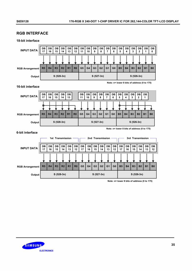
S6D0128 176-RGB X 240-DOT 1-CHIP DRIVER IC FOR 262,144-COLOR TFT-LCD DISPLAY
35
RGB INTERFACE
18-bit interface
DB
17
DB
16
DB
15
DB
14
DB
13
DB
12
DB
11
DB
10
DB
9
DB
8
DB
7
DB
6
DB
5
DB
4
DB
3
DB
2
DB
1
DB
0INPUT DATA
R5 R4 R3 R2 R1 R0 G5 G4 G3 G2 G1 G0 B5 B4 B3 B2 B1 B0RGB Arrangement
Output
Note: n= lower 8 bits of address (0 to 175)
S (528-3n) S (527-3n) S (526-3n)
16-bit interface
DB
17
DB
16
DB
15
DB
14
DB
13
DB
9
DB
11
DB
10
DB
8
DB
7
DB
6
DB
5
DB
4
DB
3
DB
2
DB
1INPUT DATA
R5 R4 R3 R2 R1 R0 G5 G4 G3 G2 G1 G0 B5 B4 B3 B2 B1 B0RGB Arrangement
Output
Note: n= lower 8 bits of address (0 to 175)
S (528-3n) S (527-3n) S (526-3n)
6-bit interface
DB
17
DB
16
DB
15
DB
14
DB
13
DB
12INPUT DATA
R5 R4 R3 R2 R1 R0 G5 G4 G3 G2 G1 G0 B5 B4 B3 B2 B1 B0RGB Arrangement
Output
Note: n= lower 8 bits of address (0 to 175)
1st Transmission 2nd Transmission 3rd Transmission
DB
17
DB
16
DB
15
DB
14
DB
13
DB
12
DB
17
DB
16
DB
15
DB
14
DB
13
DB
12
S (528-3n) S (527-3n) S (526-3n)
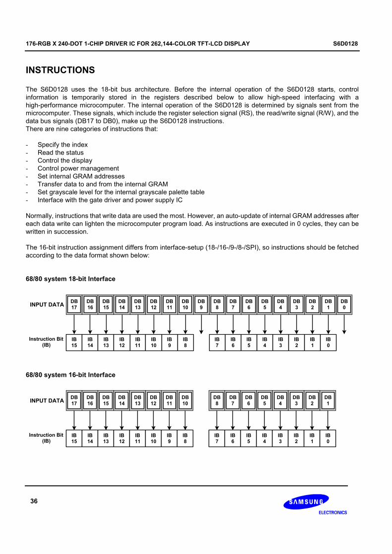
176-RGB X 240-DOT 1-CHIP DRIVER IC FOR 262,144-COLOR TFT-LCD DISPLAY S6D0128
36
INSTRUCTIONS
The S6D0128 uses the 18-bit bus architecture. Before the internal operation of the S6D0128 starts, control
information is temporarily stored in the registers described below to allow high-speed interfacing with a
high-performance microcomputer. The internal operation of the S6D0128 is determined by signals sent from the
microcomputer. These signals, which include the register selection signal (RS), the read/write signal (R/W), and the
data bus signals (DB17 to DB0), make up the S6D0128 instructions.
There are nine categories of instructions that:
- Specify the index
- Read the status
- Control the display
- Control power management
- Set internal GRAM addresses
- Transfer data to and from the internal GRAM
- Set grayscale level for the internal grayscale palette table
- Interface with the gate driver and power supply IC
Normally, instructions that write data are used the most. However, an auto-update of internal GRAM addresses after
each data write can lighten the microcomputer program load. As instructions are executed in 0 cycles, they can be
written in succession.
The 16-bit instruction assignment differs from interface-setup (18-/16-/9-/8-/SPI), so instructions should be fetched
according to the data format shown below:
68/80 system 18-bit Interface
DB
17INPUT DATA
Instruction Bit
(IB)
DB
16
DB
15
DB
14
DB
13
DB
12
DB
11
DB
10
DB
9
DB
8
DB
7
DB
6
DB
5
DB
4
DB
3
DB
2
DB
1
DB
0
IB
15
IB
14
IB
13
IB
12
IB
11
IB
10
IB
9
IB
8
IB
7
IB
6
IB
5
IB
4
IB
3
IB
2
IB
1
IB
0
68/80 system 16-bit Interface
DB
17INPUT DATA
Instruction Bit
(IB)
DB
16
DB
15
DB
14
DB
13
DB
12
DB
11
DB
10
DB
8
DB
7
DB
6
DB
5
DB
4
DB
3
DB
2
DB
1
IB
15
IB
14
IB
13
IB
12
IB
11
IB
10
IB
9
IB
8
IB
7
IB
6
IB
5
IB
4
IB
3
IB
2
IB
1
IB
0

S6D0128 176-RGB X 240-DOT 1-CHIP DRIVER IC FOR 262,144-COLOR TFT-LCD DISPLAY
37
68/80 system 9-bit Interface
1st Transmission 2nd Transmission
DB
17INPUT DATA
Instruction Bit
(IB)
DB
16
DB
15
DB
14
DB
13
DB
12
DB
11
DB
10
DB
9
IB
15
IB
14
IB
13
IB
12
IB
11
IB
10
IB
9
IB
8
IB
7
IB
6
IB
5
IB
4
IB
3
IB
2
IB
1
IB
0
DB
17
DB
16
DB
15
DB
14
DB
13
DB
12
DB
11
DB
10
DB
9
68/80 system 8-bit Interface
DB
17INPUT DATA
Instruction Bit
(IB)
DB
16
DB
15
DB
14
DB
13
DB
12
DB
11
DB
10
IB
15
IB
14
IB
13
IB
12
IB
11
IB
10
IB
9
IB
8
IB
7
IB
6
IB
5
IB
4
IB
3
IB
2
IB
1
IB
0
1st Transmission 2nd Transmission
DB
17
DB
16
DB
15
DB
14
DB
13
DB
12
DB
11
DB
10
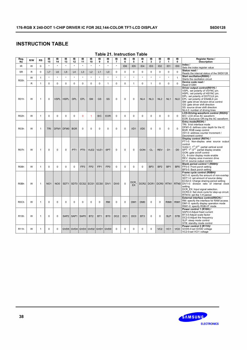
176-RGB X 240-DOT 1-CHIP DRIVER IC FOR 262,144-COLOR TFT-LCD DISPLAY S6D0128
38
INSTRUCTION TABLE
Table 21. Instruction Table Reg. No
R/W RS IB 15
IB 14
IB 13
IB 12
IB 11
IB 10
IB 9
IB 8
IB 7
IB 6
IB 5
IB 4
IB 3
IB 2
IB 1
IB 0
Register Name / Description
IR W 0 * * * * * * * * * ID6 ID5 ID4 ID3 ID2 ID1 ID0 Index / Sets the index register value
SR R 0 L7 L6 L5 L4 L3 L2 L1 L0 0 0 0 0 0 0 0 0 Status read / Reads the internal status of the S6D0128
W 1 * * * * * * * * * * * * * * * 1 Start oscillation(R00H) / Starts the oscillation circuit
R00h
R 1 0 0 0 0 0 0 0 1 0 0 1 0 1 0 0 0 Device code read / Read 0128H
R01h W 1 0 VSPL HSPL DPL EPL SM GS SS 0 0 0 NL4 NL3 NL2 NL1 NL0
Driver output control(R01H) / VSPL: set polarity of VSYNC pin. HSPL: set polarity of HSYNC pin. DPL: set polarity of DOTCLK pin. EPL: set polarity of ENABLE pin SM: gate driver division drive control GS: gate driver shift direction SS: source driver shift direction NL4-0: number of driving lines
R02h W 1 0 0 0 0 0 1 B/C EOR 0 0 0 0 0 0 0 0 LCD-Driving-waveform control (R02H)/ B/C: LCD drive AC waveform EOR: Exclusive OR-ing the AC waveform
R03h W 1 TRI DFM1 DFM0 BGR 0 0 0 0 0 0 I/D1 I/D0 0 0 0 0
Entry mode(R03H) / TRI: 8-bit interface mode DFM1-0: defines color depth for the IC BGR: RGB swap control I/D1-0: address counter Increment / Decrement control
R07h W 1 0 0 0 PT1 PT0 VLE2 VLE1 SPT 0 0 0 GON CL REV D1 D0
Display control (R07H) / PT1-0: Non-display area source output control VLE2-1: 1
st /2
nd partial vertical scroll
SPT: 1st /2
nd partial display enable
GON: gate on/off control CL: 8-color display mode enable REV: display area inversion drive D1-0: source output control
R08h W 1 0 0 0 0 FP3 FP2 FP1 FP0 0 0 0 0 BP3 BP2 BP1 BP0 Blank period control 1 (R08H)/ FP3-0: Front porch setting BP3-0: Back porch setting
R0Bh W 1 NO1 NO0 SDT1 SDT0 ECS2 ECS1 ECS0 DIV1 DIV0 0 DCR_EX
DCR2 DCR1 DCR0 RTN1 RTN0
Frame cycle control (R0BH)/ NO1-0: specify the amount of non-overlap SDT1-0: set amount of source delay ECS2-0: Charge sharing period setting DIV1-0: division ratio of internal clock setting DCR_EX: Input signal selection. DCR2-0: Set clock cycle for step-up circuit. RTN10: set the 1-H period
R0Ch W 1 0 0 0 0 0 0 0 RM 0 0 DM1 DM0 0 0 RIM0 RIM1
External interface control(R0CH) / RM: specify the interface for RAM access DM1-0: specify display operation mode RIM1-0: specify RGB-I/F mode
R10h W 1 0 0 SAP2 SAP1 SAP0 BT2 BT1 BT0 DC2 DC1 DC0 BT3 0 0 SLP STB
Power control 1 (R10H) / SAP2-0:Adjust fixed current BT3-0:Adjust scale factor DC2-0:Adjust the frequency SLP: sleep mode control STB: standby mode control
R11h W 1 0 0 GVD5 GVD4 GVD3 GVD2 GVD1 GVD0 0 0 0 0 0 VC2 VC1 VC0 Power control 2 (R11H)/ GVD5-0:set GVDD voltage VC2-0:set VCI1 voltage

S6D0128 176-RGB X 240-DOT 1-CHIP DRIVER IC FOR 262,144-COLOR TFT-LCD DISPLAY
39
Table 22. Instruction Table (Continued)
Reg. No
R/W RS IB 15
IB 14
IB 13
IB 12
IB 11
IB 10
IB 9
IB 8
IB 7
IB 6
IB 5
IB 4
IB 3
IB 2
IB 1
IB 0
Register Name / Description
R13h W 1 0 0 0 0 0 0 0 0 0 PON PON1 AON 0 0 0 0
Power control 3 (R13H)/ PON: step-up circuit control PON1: step-up circuit control AON: operation start bit for the amplifier.
R14h W 1 0 VCMR
VCM5 VCM4 VCM3 VCM2 VCM1 VCM0 0 0 VML5 VML4 VML3 VML2 VML1 VML0
Power control 4 (R14H)/ VCMR: VCOMH control VCM5-0:set the VCOMH voltage VML5-0:set the VCOM Amplitude
R21h W 1 AD15 AD14 AD13 AD12 AD11 AD10 AD9 AD8 AD7 AD6 AD5 AD4 AD3 AD2 AD1 AD0 RAM address set (R21H)/ AD15-0: set GRAM address.
W 1 WD17-0 : Pin assignment varies according to the interface method Write data to GRAM (R22H)/ WD17-0:Input data for GRAM
R22h
R 1 RD17-0 : Pin assignment varies according to the interface method Read data from GRAM (R22H)/ RD17-0:Read data from GRAM
R30h W 1 0 0 0 0 0 PKP 12
PKP 11
PKP 10
0 0 0 0 0 PKP 02
PKP 01
PKP 00
Gamma control 1 (R30H)/ Adjust Gamma voltage
R31h W 1 0 0 0 0 0 PKP 32
PKP 31
PKP 30
0 0 0 0 0 PKP 22
PKP 21
PKP 20
Gamma control 2 (R31H)/ Adjust Gamma voltage
R32h W 1 0 0 0 0 0 PKP 52
PKP 51
PKP 50
0 0 0 0 0 PKP 42
PKP 41
PKP 40
Gamma control 3 (R32H)/ Adjust Gamma voltage
R33h W 1 0 0 0 0 0 PRP 12
PRP 11
PRP 10
0 0 0 0 0 PRP 02
PRP 01
PRP 00
Gamma control 4 (R33H)/ Adjust Gamma voltage
R34h W 1 0 0 0 0 0 PKN 12
PKN 11
PKN 10
0 0 0 0 0 PKN 02
PKN 01
PKN 00
Gamma control 5 (R34H)/ Adjust Gamma voltage
R35h W 1 0 0 0 0 0 PKN 32
PKN 31
PKN 30
0 0 0 0 0 PKN 22
PKN 21
PKN 20
Gamma control 6 (R35H)/ Adjust Gamma voltage
R36h W 1 0 0 0 0 0 PKN 52
PKN 51
PKN 50
0 0 0 0 0 PKN 42
PKN 41
PKN 40
Gamma control 7 (R36H)/ Adjust Gamma voltage
R37h W 1 0 0 0 0 0 PRN 12
PRN 11
PRN 10
0 0 0 0 0 PRN 02
PRN 01
PRN 00
Gamma control 8 (R37H)/ Adjust Gamma voltage
R38h W 1 0 0 0 VRP 14
VRP 13
VRP 12
VRP 11
VRP 10
0 0 0 0 VRP 03
VRP 02
VRP 01
VRP 00
Gamma control 9 (R38H)/ Adjust Gamma voltage
R39h W 1 0 0 0 VRN 14
VRN 13
VRN 12
VRN 11
VRN 10
0 0 0 0 VRN 03
VRN 02
VRN 01
VRN 00
Gamma control 10 (R39H)/ Adjust Gamma voltage
R40h W 1 0 0 0 0 0 0 0 0 0 0 0 SCN4 SCN3 SCN2 SCN1 SCN0 Gate scan position (R40H)/ SCN4-0: scan starting position of gate
R41h W 1 0 0 0 0 0 0 0 0 VL7 VL6 VL5 VL4 VL3 VL2 VL1 VL0 Vertical scroll control (R41H)/ VL7-0:
R42h W 1 SE17 SE16 SE15 SE14 SE13 SE12 SE11 SE10 SS17 SS16 SS15 SS14 SS13 SS12 SS11 SS10 1
st screen driving position (R42H)/
SE17-10: 1st screen start position
SS17-10: 1st screen end position
R43h W 1 SE27 SE26 SE25 SE24 SE23 SE22 SE21 SE20 SS27 SS26 SS25 SS24 SS23 SS22 SS21 SS20 2
nd screen driving position (R43H)/
SE27-20: 2nd screen start position
SS27-20: 2nd screen end position
R44h W 1 HEA7 HEA6 HEA5 HEA4 HEA3 HEA2 HEA1 HEA0 HSA7 HSA6 HSA5 HSA4 HSA3 HSA2 HSA1 HSA0
Horizontal window address (R44H)/ HEA7-0: Horizontal window address end position HSA7-0: Horizontal window address start position
R45h W 1 VEA7 VEA6 VEA5 VEA4 VEA3 VEA2 VEA1 VEA0 VSA7 VSA6 VSA5 VSA4 VSA3 VSA2 VSA1 VSA0
Vertical window Address (R45H)/ VEA7-0: Vertical window address end position VSA7-0: Vertical window address start position
R71h W 1 Test command1 Don’t use this command
R72h W 1 Test command2 Don’t use this command
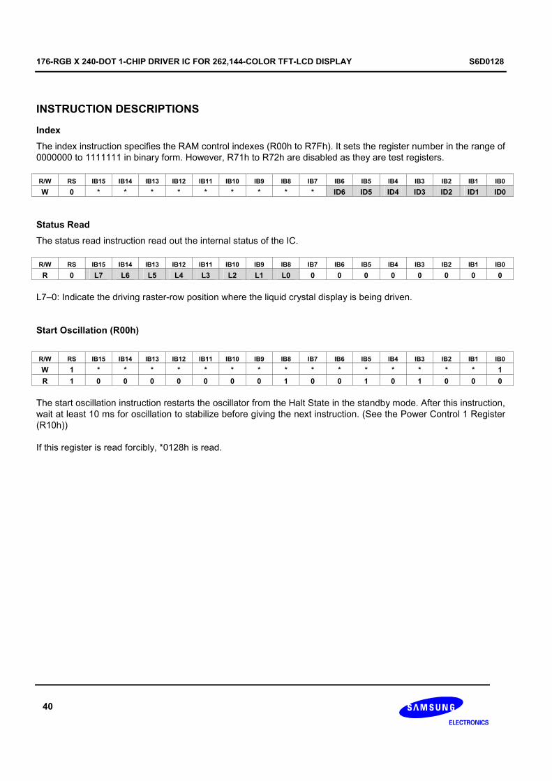
176-RGB X 240-DOT 1-CHIP DRIVER IC FOR 262,144-COLOR TFT-LCD DISPLAY S6D0128
40
INSTRUCTION DESCRIPTIONS
Index
The index instruction specifies the RAM control indexes (R00h to R7Fh). It sets the register number in the range of
0000000 to 1111111 in binary form. However, R71h to R72h are disabled as they are test registers.
R/W RS IB15 IB14 IB13 IB12 IB11 IB10 IB9 IB8 IB7 IB6 IB5 IB4 IB3 IB2 IB1 IB0
W 0 * * * * * * * * * ID6 ID5 ID4 ID3 ID2 ID1 ID0
Status Read
The status read instruction read out the internal status of the IC.
R/W RS IB15 IB14 IB13 IB12 IB11 IB10 IB9 IB8 IB7 IB6 IB5 IB4 IB3 IB2 IB1 IB0
R 0 L7 L6 L5 L4 L3 L2 L1 L0 0 0 0 0 0 0 0 0
L7–0: Indicate the driving raster-row position where the liquid crystal display is being driven.
Start Oscillation (R00h)
R/W RS IB15 IB14 IB13 IB12 IB11 IB10 IB9 IB8 IB7 IB6 IB5 IB4 IB3 IB2 IB1 IB0
W 1 * * * * * * * * * * * * * * * 1
R 1 0 0 0 0 0 0 0 1 0 0 1 0 1 0 0 0
The start oscillation instruction restarts the oscillator from the Halt State in the standby mode. After this instruction,
wait at least 10 ms for oscillation to stabilize before giving the next instruction. (See the Power Control 1 Register
(R10h))
If this register is read forcibly, *0128h is read.

S6D0128 176-RGB X 240-DOT 1-CHIP DRIVER IC FOR 262,144-COLOR TFT-LCD DISPLAY
41
Driver Output Control (R01h)
R/W RS IB15 IB14 IB13 IB12 IB11 IB10 IB9 IB8 IB7 IB6 IB5 IB4 IB3 IB2 IB1 IB0
W 1 0 VSPL HSPL DPL EPL SM GS SS 0 0 0 NL4 NL3 NL2 NL1 NL0
VSPL: reverses the polarity of the VSYNC signal.
VSPL= “0”: VSYNC is low active.
VSPL= “1”: VSYNC is high active.
HSPL: reverses the polarity of the HSYNC signal.
HSPL= “0”: HSYNC is low active.
HSPL= “1”: HSYNC is high active.
DPL: reverses the polarity of the DOTCLK signal.
DPL= “0”: Display data is fetched at DOTCLK’s rising edge.
DPL= “1”: Display data is fetched at DOTCLK’s falling edge.
EPL: Set the polarity of ENABLE pin while using RGB interface.
EPL = “0”: ENABLE = ”Low” / write data of DB17-0
ENABLE = ”High” / don’t write data of DB17-0
EPL = “1”: ENABLE = ”High” / write data of DB17-0
ENABLE = ”Low” / don’t write data of DB17-0
Table 23. Relationship between EPL, ENABLE and RAM access
EPL ENABLE RAM write RAM address
0 0 Valid Updated
0 1 Invalid Held
1 1 Valid Updated
1 0 Invalid Held
GS: Selects the output shift direction of the gate driver. When GS = 0, G1 shifts to G240. When GS = 1, G240 shifts
to G1.
SM: Select the division drive method of the gate driver. When SM = 0, even/odd division is selected; SM = 1,
upper/lower division drive is selected. Various connections between TFT panel and the IC can be supported with the
combination of SM and GS bit.
SS: Selects the output shift direction of the source driver. When SS = 0, S1 shifts to S528. When SS = 1, S528 shifts
to S1. In addition, SS and BGR bits should be specified in case of the RGB order is changed. When SS = 0 and BGR
= 0, <R><G><B> are assigned in order from S1 pin. When SS = 1 and BGR = 1, <R><G><B> are assigned in order
from S528. Re-write data to GRAM whenever SS and BGR bit are changed.
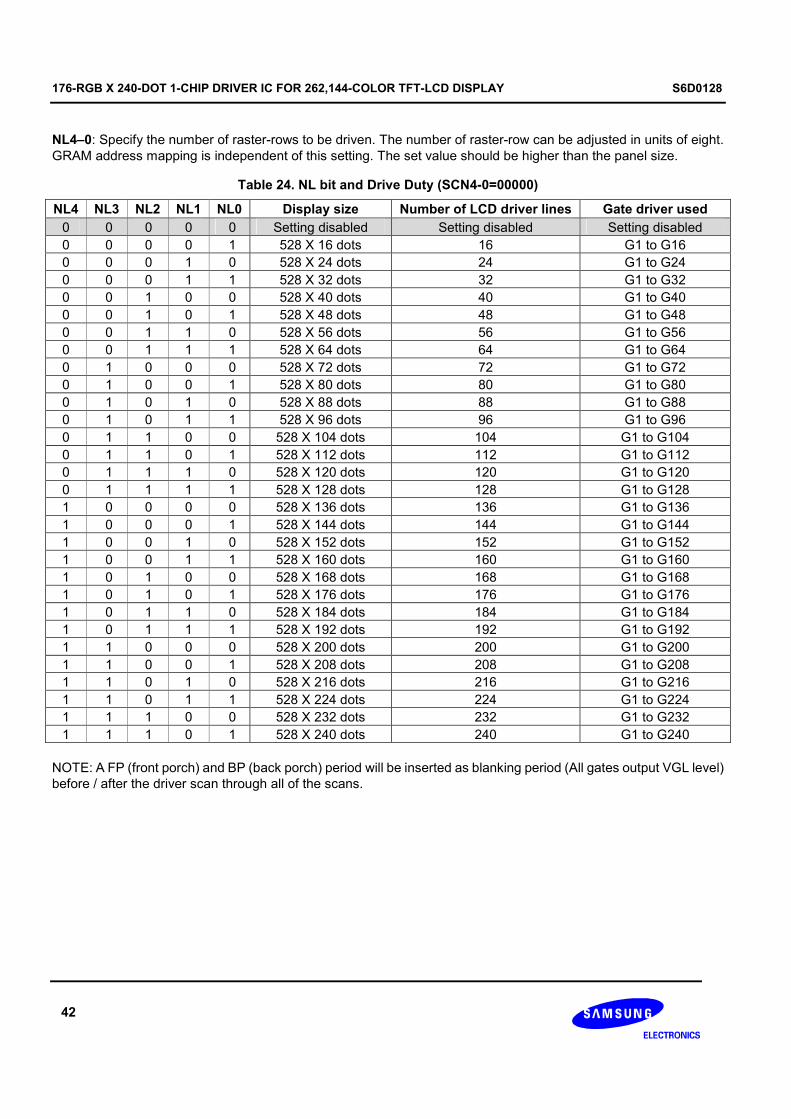
176-RGB X 240-DOT 1-CHIP DRIVER IC FOR 262,144-COLOR TFT-LCD DISPLAY S6D0128
42
NL4–0: Specify the number of raster-rows to be driven. The number of raster-row can be adjusted in units of eight.
GRAM address mapping is independent of this setting. The set value should be higher than the panel size.
Table 24. NL bit and Drive Duty (SCN4-0=00000)
NL4 NL3 NL2 NL1 NL0 Display size Number of LCD driver lines Gate driver used
0 0 0 0 0 Setting disabled Setting disabled Setting disabled
0 0 0 0 1 528 X 16 dots 16 G1 to G16
0 0 0 1 0 528 X 24 dots 24 G1 to G24
0 0 0 1 1 528 X 32 dots 32 G1 to G32
0 0 1 0 0 528 X 40 dots 40 G1 to G40
0 0 1 0 1 528 X 48 dots 48 G1 to G48
0 0 1 1 0 528 X 56 dots 56 G1 to G56
0 0 1 1 1 528 X 64 dots 64 G1 to G64
0 1 0 0 0 528 X 72 dots 72 G1 to G72
0 1 0 0 1 528 X 80 dots 80 G1 to G80
0 1 0 1 0 528 X 88 dots 88 G1 to G88
0 1 0 1 1 528 X 96 dots 96 G1 to G96
0 1 1 0 0 528 X 104 dots 104 G1 to G104
0 1 1 0 1 528 X 112 dots 112 G1 to G112
0 1 1 1 0 528 X 120 dots 120 G1 to G120
0 1 1 1 1 528 X 128 dots 128 G1 to G128
1 0 0 0 0 528 X 136 dots 136 G1 to G136
1 0 0 0 1 528 X 144 dots 144 G1 to G144
1 0 0 1 0 528 X 152 dots 152 G1 to G152
1 0 0 1 1 528 X 160 dots 160 G1 to G160
1 0 1 0 0 528 X 168 dots 168 G1 to G168
1 0 1 0 1 528 X 176 dots 176 G1 to G176
1 0 1 1 0 528 X 184 dots 184 G1 to G184
1 0 1 1 1 528 X 192 dots 192 G1 to G192
1 1 0 0 0 528 X 200 dots 200 G1 to G200
1 1 0 0 1 528 X 208 dots 208 G1 to G208
1 1 0 1 0 528 X 216 dots 216 G1 to G216
1 1 0 1 1 528 X 224 dots 224 G1 to G224
1 1 1 0 0 528 X 232 dots 232 G1 to G232
1 1 1 0 1 528 X 240 dots 240 G1 to G240
NOTE: A FP (front porch) and BP (back porch) period will be inserted as blanking period (All gates output VGL level)
before / after the driver scan through all of the scans.
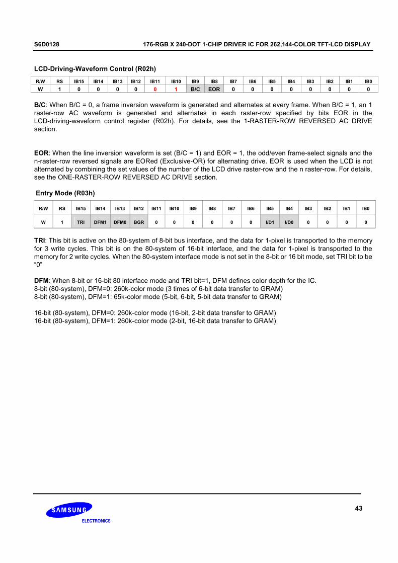
S6D0128 176-RGB X 240-DOT 1-CHIP DRIVER IC FOR 262,144-COLOR TFT-LCD DISPLAY
43
LCD-Driving-Waveform Control (R02h)
R/W RS IB15 IB14 IB13 IB12 IB11 IB10 IB9 IB8 IB7 IB6 IB5 IB4 IB3 IB2 IB1 IB0
W 1 0 0 0 0 0 1 B/C EOR 0 0 0 0 0 0 0 0
B/C: When B/C = 0, a frame inversion waveform is generated and alternates at every frame. When B/C = 1, an 1
raster-row AC waveform is generated and alternates in each raster-row specified by bits EOR in the
LCD-driving-waveform control register (R02h). For details, see the 1-RASTER-ROW REVERSED AC DRIVE
section.
EOR: When the line inversion waveform is set (B/C = 1) and EOR = 1, the odd/even frame-select signals and the
n-raster-row reversed signals are EORed (Exclusive-OR) for alternating drive. EOR is used when the LCD is not
alternated by combining the set values of the number of the LCD drive raster-row and the n raster-row. For details,
see the ONE-RASTER-ROW REVERSED AC DRIVE section.
Entry Mode (R03h)
R/W RS IB15 IB14 IB13 IB12 IB11 IB10 IB9 IB8 IB7 IB6 IB5 IB4 IB3 IB2 IB1 IB0
W 1 TRI DFM1 DFM0 BGR 0 0 0 0 0 0 I/D1 I/D0 0 0 0 0
TRI: This bit is active on the 80-system of 8-bit bus interface, and the data for 1-pixel is transported to the memory
for 3 write cycles. This bit is on the 80-system of 16-bit interface, and the data for 1-pixel is transported to the
memory for 2 write cycles. When the 80-system interface mode is not set in the 8-bit or 16 bit mode, set TRI bit to be
“0”
DFM: When 8-bit or 16-bit 80 interface mode and TRI bit=1, DFM defines color depth for the IC.
8-bit (80-system), DFM=0: 260k-color mode (3 times of 6-bit data transfer to GRAM)
8-bit (80-system), DFM=1: 65k-color mode (5-bit, 6-bit, 5-bit data transfer to GRAM)
16-bit (80-system), DFM=0: 260k-color mode (16-bit, 2-bit data transfer to GRAM)
16-bit (80-system), DFM=1: 260k-color mode (2-bit, 16-bit data transfer to GRAM)

176-RGB X 240-DOT 1-CHIP DRIVER IC FOR 262,144-COLOR TFT-LCD DISPLAY S6D0128
44
Table 26. TRI and DFM1-0 setting
TRI DFM1 DFM0 Write data to GRAM
0 0 0 80-system 8bit interface
DB
17
DB
16
DB
15
DB
14
DB
13
DB
12
DB
11
DB
10
DB
17
DB
16
DB
15
DB
14
DB
13
DB
12
DB
11
DB
10GRAM DATA
R5 R4 R3 R2 R1 R0
S (3n + 1)
G5 G4 G3 G2 G1 G0
S (3n + 2)
B5 B4 B3 B2 B1 B0
S (3n + 3)
RGB Arrangement
Output
Note: n= lower 8 byte of address (0 to 175)
1st Transmission 2nd Transmission
0 * * Setting disabled
1 0 * Setting disabled
1 1 0 80-system 8bit interface
DB
17
DB
16
DB
15
DB
14
DB
13
DB
12
DB
17
DB
16
DB
15GRAM DATA
R5 R4 R3 R2 R1 R0
S (3n + 1)
G5 G4 G3 G2 G1 G0
S (3n + 2)
B5 B4 B3 B2 B1 B0
S (3n + 3)
RGB Arrangement
Output
Note: n= lower 8 byte of address (0 to 175)
DB
14
DB
13
DB
12
DB
17
DB
16
DB
15
DB
14
DB
13
DB
12
1st Transmission 2nd Transmission 3rd Transmission
1 1 1 80-system 8bit interface
DB
17
DB
16
DB
15
DB
14
DB
13
DB
12
DB
17
DB
16
DB
15GRAM DATA
R5 R4 R3 R2 R1 R0
S (3n + 1)
G5 G4 G3 G2 G1 G0
S (3n + 2)
B5 B4 B3 B2 B1 B0
S (3n + 3)
RGB Arrangement
Output
Note: n= lower 8 byte of address (0 to 175)
DB
14
DB
13
DB
12
DB
17
DB
16
DB
15
DB
14
DB
13
DB
12
1st Transmission 2nd Transmission 3rd Transmission

S6D0128 176-RGB X 240-DOT 1-CHIP DRIVER IC FOR 262,144-COLOR TFT-LCD DISPLAY
45
TRI DFM1 DFM0 Write data to GRAM
0 0 0 80-system 16bit interface
DB
17
DB
16
DB
15
DB
14
DB
13
DB
12
DB
11
DB
10
DB
8
DB
7
DB
6
DB
5
DB
4
DB
3
DB
2
DB
1GRAM DATA
R5 R4 R3 R2 R1 R0 G5 G4 G3 G2 G1 G0 B5 B4 B3 B2 B1 B0RGB Arrangement
Output
Note: n= lower 8 bits of address (0 to 175)
S (3n+1) S (3n+2) S (3n+3)
0 * * Setting disabled
1 0 * Setting disabled
1 1 0 80-system 16bit interface
1 1 1 80-system 16bit interface

176-RGB X 240-DOT 1-CHIP DRIVER IC FOR 262,144-COLOR TFT-LCD DISPLAY S6D0128
46
I/D1-0: When I/D1-0 = 1, the address counter (AC) is automatically increased by 1 after the data is written to the
GRAM. When I/D1-0 = 0, the AC is automatically decreased by 1 after the data is written to the GRAM. Automatic
address counter updating is not performed when reading data from GRAM. The increment/decrement setting of the
address counter by I/D1-0 bits is performed independently for the upper (AD15-8) and lower (AD7-0) addresses.
Table 27. Address Direction Setting
I/D1-0=”00”
H: decrement
V: decrement
I/D1-0=”01”
H: increment
V: decrement
I/D1-0=”10”
H: decrement
V: increment
I/D1-0=”11”
H: increment
V: increment
BGR: About writing 18-bit data to GRAM, it is changed <R><G><B> into <B><G><R>.
- BGR = 0 ; DB[17:12], DB[11:6], DB[5:0] is assigned to R, G, B.
- BGR = 1 ; DB[17:12], DB[11:6], DB[5:0] is assigned to B, G, R.
DB
17
DB
16
DB
15
DB
14
DB
13
DB
12
DB
11
DB
10
DB
9
DB
8
DB
7
DB
6
DB
5
DB
4
DB
3
DB
2
DB
1
DB
0Write Data to
GRAM *1
18 bits
Conversion of RGB to BGR (vice versa)
GRAM
Figure 5. Write data to GRAM via RGB swapping block

S6D0128 176-RGB X 240-DOT 1-CHIP DRIVER IC FOR 262,144-COLOR TFT-LCD DISPLAY
47
Display Control (R07h)
R/W RS IB15 IB14 IB13 IB12 IB11 IB10 IB9 IB8 IB7 IB6 IB5 IB4 IB3 IB2 IB1 IB0
W 1 0 0 0 PT1 PT0 VLE2 VLE1 SPT 0 0 0 GON CL REV D1 D0
PT1-0: Normalize the source outputs when non-displayed area of the partial display is driven. For details, see the
SCREEN-DIVISION DRIVING FUNCTION section.
Source Output on
Non-display Area
VCOM Output on
Non-display Area PT1 PT0
Positive Negative Positive Negative
Gate Output for Non-display Area
0 0 AVSS AVSS AVSS AVSS Normal Scan
0 1 AVSS GVDD VCOML VCOMH Normal Scan
1 0 GVDD AVSS VCOML VCOMH Normal Scan
1 1 Hi-z Hi-z AVSS AVSS Normal Scan
VLE2–1: When VLE1 = 1, a vertical scroll is performed in the 1st screen. When VLE2 = 1, a vertical scroll is
performed in the 2nd screen. Vertical scrolling on the two screens cannot be controlled at the same time.
VLE2 VLE1 2nd
Screen 1st
Screen
0 0 Fixed display Fixed display
0 1 Fixed display Scroll
1 0 Scroll Fixed display
1 1 Setting disabled Setting disabled
SPT: When SPT = 1, the 2-division LCD drive is performed. For details, see the SCREEN-DIVISION DRIVING
FUNCTION section.
Note: this function is not available when the external display interface (i.e. RGB interface or VSYNC interface) is in use.
GON: Gate on/off control signal. All gate output is set to be gate off level when GON = 0.
When GON = 1, gate driver is working: G1 to G240 output is either VGH or VGL level. See the Instruction
Set up flow for further description on the display on/off flow.
GON Gate Output
0 All gate off (All gates output are set to VGL)
1 Gate on(VGH / VGL)
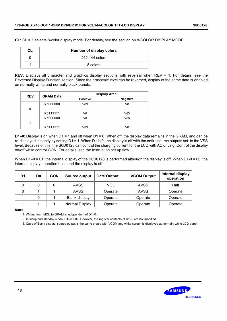
176-RGB X 240-DOT 1-CHIP DRIVER IC FOR 262,144-COLOR TFT-LCD DISPLAY S6D0128
48
CL: CL = 1 selects 8-color display mode. For details, see the section on 8-COLOR DISPLAY MODE.
CL Number of display colors
0 262,144 colors
1 8 colors
REV: Displays all character and graphics display sections with reversal when REV = 1. For details, see the
Reversed Display Function section. Since the grayscale level can be reversed, display of the same data is enabled
on normally white and normally black panels.
Display Area REV GRAM Data
Positive Negative
0
6’b000000
:
6’b111111
V63
:
V0
V0
:
V63
1
6’b000000
:
6’b111111
V0
:
V63
V63
:
V0
D1–0: Display is on when D1 = 1 and off when D1 = 0. When off, the display data remains in the GRAM, and can be
re-displayed instantly by setting D1 = 1. When D1 is 0, the display is off with the entire source outputs set to the VSS
level. Because of this, the S6D0128 can control the charging current for the LCD with AC driving. Control the display
on/off while control GON. For details, see the Instruction set up flow.
When D1–0 = 01, the internal display of the S6D0128 is performed although the display is off. When D1-0 = 00, the
internal display operation halts and the display is off.
D1 D0 GON Source output Gate Output VCOM Output Internal display
operation
0 0 0 AVSS VGL AVSS Halt
0 1 1 AVSS Operate AVSS Operate
1 0 1 Blank display Operate Operate Operate
1 1 1 Normal Display Operate Operate Operate
Notes:
1. Writing from MCU to GRAM is independent of D1–0.
2. In sleep and standby mode, D1–0 = 00. However, the register contents of D1–0 are not modified.
3. Case of Blank display, source output is the same phase with VCOM and white screen is displayed at normally white LCD panel

S6D0128 176-RGB X 240-DOT 1-CHIP DRIVER IC FOR 262,144-COLOR TFT-LCD DISPLAY
49
Display control 2 (R08h)
R/W RS IB15 IB14 IB13 IB12 IB11 IB10 IB9 IB8 IB7 IB6 IB5 IB4 IB3 IB2 IB1 IB0
W 1 0 0 0 0 FP3 FP2 FP1 FP0 0 0 0 0 BP3 BP2 BP1 BP0
The blanking period in the front and end of the display area can be defined using this register.
When N-raster-row is driving, a blank period is inserted after all screens are drawn. Front and Back porch can be
adjusted using FP3-0 and BP3-0 bits (R08h).
FP3-0/BP3-0: Set the periods of blanking (the front and back porch), which are placed at the beginning and end of
the display. FP3-0 is for a front porch and BP3-0 is for a back porch. When front and back porches are set, the
settings should meet the following conditions.
1 ≤ BP + FP ≤ 16 raster-rows
FP ≥ 0
BP ≥ 0
When the external display interface is in use, the front porch (FP) will start on the falling edge of the VSYNC signal
and display operation commences at the end of the front-porch period. The back porch (BP) will start when data for
the number of raster-rows specified by the NL bits has been displayed. During the period between the completion of
the back-porch period and the next VSYNC signal, the display will remain blank.
Table 28. Front/Back Porch
FP3
BP3
FP2
BP2
FP1
BP1
FP0
BP0
# of Raster Periods In the Front Porch
# of Raster Periods In the Back Porch
0 0 0 0 0
0 0 0 1 1
0 0 1 0 2
0 0 1 1 3
0 1 0 0 4
.
.
.
.
.
.
.
.
.
.
.
.
.
.
.
1 1 0 0 12
1 1 0 1 13
1 1 1 0 14
1 1 1 1 Setting Disabled

176-RGB X 240-DOT 1-CHIP DRIVER IC FOR 262,144-COLOR TFT-LCD DISPLAY S6D0128
50
Frame Cycle Control (R0Bh)
R/W RS IB15 IB14 IB13 IB12 IB11 IB10 IB9 IB8 IB7 IB6 IB5 IB4 IB3 IB2 IB1 IB0
W 1 NO1 NO0 SDT1 SDT0 ECS
2
ECS
1
ECS
0
DIV
1
DIV
0
0 DCR
_EX
DCR
2
DCR
1
DCR
0
RTN1 RTN0
NO1-0: Set amount of non-overlap for the gate output.
Amount of non-overlap
NO1 NO0 Internal Operation
(synchronized with internal clock)
RGB I/F Operation
(synchronized with DOTCLK)
0 0 2 clock cycle 16 clock cycle
0 1 4 clock cycle 32 clock cycle
1 0 6 clock cycle 48 clock cycle
1 1 8 clock cycle 64 clock cycle
Note: The amount of non-overlap time is defined from the falling edge of the CL1
SDT1-0: Set delay amount from gate edge (end) to source output.
Delay amount of the source output
SDT1 SDT0 Internal Operation
(synchronized with internal clock)
RGB I/F Operation
(synchronized with DOTCLK)
0 0 1 clock cycle 8 clock cycle
0 1 2 clock cycle 16 clock cycle
1 0 3 clock cycle 24 clock cycle
1 1 4 clock cycle 32 clock cycle

S6D0128 176-RGB X 240-DOT 1-CHIP DRIVER IC FOR 262,144-COLOR TFT-LCD DISPLAY
51
Figure 6. Set Delay from Gate Output to Source Output and ECS signal
Note: The values specified by the bits of ECS, SDT1-0 and NO1-0 vary in a reference clock for each interface mode.
Internal operation mode : Internal R-C oscillation clock
RGB-I/F mode : DOTCLK
VSYNC-I/F : Internal R-C oscillation clock
ECS2-0: ECS period is sustained for the number of clock cycle which is set on ECS2-0. When VCOML<0, set
these bits as “000” for preventing the abnormal function.
ECS period
ECS2 ECS1 ECS0 Internal Operation
(synchronized with internal clock)
RGB I/F Operation
(synchronized with DOTCLK)
0 0 0 No ECS No ECS
0 0 1 2 clock cycle 8 clock cycle
0 1 0 4 clock cycle 16 clock cycle
0 1 1 6 clock cycle 24 clock cycle
1 0 0 8 clock cycle 32 clock cycle
1 0 1 12 clock cycle 48 clock cycle
1 1 0 14 clock cycle 56 clock cycle
1 1 1 Setting disabled Setting disabled

176-RGB X 240-DOT 1-CHIP DRIVER IC FOR 262,144-COLOR TFT-LCD DISPLAY S6D0128
52
DIV1-0: Set the division ratio of clocks for internal operation (DIV1-0). Internal operations are driven by clocks, which
are frequency divided according to the DIV1-0 setting. Frame frequency can be adjusted along with the 1H period
(RTN3-0). When changing number of the drive cycle, adjust the frame frequency. For details, see the Frame
Frequency Adjustment Function section.
DIV1 DIV0 Division Ratio Internal operation clock frequency(INCLK)
0 0 1 fosc/1
0 1 2 fosc/2
1 0 4 fosc/4
1 1 8 fosc/8
*fosc = R-C oscillation frequency
Frame Frequency =fOSC
Clock cycles per raster-row x division ratio x (Line+B)[Hz]
fOSC: R-C oscillation frequency
Line: Number of raster-rows (NL bit)
Clock cycles per raster-row: RTN bit
Division ratio: DIV bit
B: Blank period(Back porch + Front Porch)
Figure 7. Formula for the frame frequency
DCR_EX: Input signal selection signal for external interface mode. (0: internal operation clock, 1: DOTCLK)
Set DCR_EX bit to 1 for DOTCLK to be DCCLK (clock cycle for step-up circuit) source when external interface mode
is in use (DM[1:0]=”01”).
DCR 2-0: Set clock cycle for step-up circuit in external interface mode. Please set DCR_EX bit to “1” and DCR1-0
value when external interface is in use. In this case, DOTCLK must be input periodically and continuously.
DCR2 DCR1 DCR0 Clock cycle for step-up circuits (DCCLK) in external interface mode
0 0 0 DOTCLK/32
0 0 1 DOTCLK/64
0 1 0 DOTCLK/128
0 1 1 DOTCLK/256
1 * * DOTCLK/512
Note: If DOTCLK input cycle is variable or discontinuous, clock cycle for step-up circuit must be generated internally (DCR_EX=0).
RTN1-0: Set the 1H period (1 raster-row).
RTN1 RTN0 Horizontal clock frequency(CL1) Clock frequency for step-up circuits(DCCLK)
0 0 INCLK/16 fosc/8
0 1 INCLK/20 fosc/10
1 0 INCLK/24 fosc/12
1 1 INCLK/28 fosc/14

S6D0128 176-RGB X 240-DOT 1-CHIP DRIVER IC FOR 262,144-COLOR TFT-LCD DISPLAY
53
External Display Interface Control (R0Ch) R/W RS IB15 IB14 IB13 IB12 IB11 IB10 IB9 IB8 IB7 IB6 IB5 IB4 IB3 IB2 IB1 IB0
W 1 0 0 0 0 0 0 0 RM 0 0 DM1 DM0 0 0 RIM1 RIM0
RM: Specifies the interface for RAM accesses. RAM accesses can be performed through the interface specified by
the bits of RIM1-0. When the display data is written via the RGB interface, 1 should be set. This bit and the DM bits
can be set independently. The display data can be written via the system interface by clearing this bit while the RGB
interface is used.
RM Interface for RAM Access
0 System interface / VSYNC interface
1 RGB interface
DM1-0: Specify the display operation mode. The interface can be set based on the bits of DM1-0. This setting
enables switching interface between internal operation and the external display interface.
Switching between two external display interfaces (RGB interface and VSYNC interface) should not be done.
DM1 DM0 Display Operation Mode
0 0 Internal clock operation
0 1 RGB interface
1 0 VSYNC interface
1 1 Setting disabled
RIM1-0: Specify the RGB interface mode when the RGB interface is used. Specifically, this setting specifies the
mode when the bits of DM and RM are set to RGB interface. These bits should be set before display operation
through the RGB interface and should not be set during operation.
RIM1 RIM0 RGB Interface Mode
0 0 18-bit RGB interface (one transfer/pixel)
0 1 16-bit RGB interface (one transfer /pixel)
1 0 6-bit RGB interface (three transfers /pixel)
1 1 Setting disabled

176-RGB X 240-DOT 1-CHIP DRIVER IC FOR 262,144-COLOR TFT-LCD DISPLAY S6D0128
54
Depending on the external display interface setting, various interfaces can be specified to match the display state.
While displaying motion pictures (RGB interface/VSYNC interface), the data for display can be written in high-speed
write mode, which achieves both low power consumption and high-speed access.
Table 29. Display State and Interface
Display State Operation Mode RAM Access (RM) Display Operation Mode
(DM1-0)
Still Pictures Internal Clock System interface
(RM=0)
Internal clock
(DM1-0=00)
Motion Pictures RGB interface (1) RGB interface
(RM=1)
RGB interface
(DM1-0=01)
Rewrite still picture area while
displaying motion pictures RGB interface (2)
System interface
(RM=0)
RGB interface
(DM1-0=01)
Motion Picture Display VSYNC interface System interface
(RM=0)
VSYNC interface
(DM1-0=10)
NOTE: 1) The instruction register can only be set through the system interface.
2) Switching between RGB interface and VSYNC interface cannot be done.
3) The RGB interface mode should not be set during operation.
4) For the transition flow for each operation mode, see the External Display Interface section.
Internal Clock Mode
All display operation is controlled by signals generated by the internal clock in internal clock mode.
All inputs through the external display interface are invalid. The internal RAM can be accessed only via the system
interface.
RGB Interface Mode (1)
The display operations are controlled by the frame synchronization clock (VSYNC), raster-row synchronization
signal (HSYNC), and dot clock (DOTCLK) in RGB interface mode. These signals should be supplied during display
operation in this mode.
The display data is transferred to the internal RAM via DB17-0 for each pixel. Combining the function of the
high-speed write mode and the window address enables display of both the motion picture area and the internal
RAM area simultaneously. In this method, data is only transferred when the screen is updated, which reduces the
amount of data transferred.
The periods of the front (FP), back (BP) porch, and the display are automatically generated in the S6D0128 by
counting the raster-row synchronization signal (HSYNC) based on the frame synchronization signal (VSYNC).
RGB Interface Mode (2)
When RGB interface is in use, data can be written to RAM via the system interface. This write operation should be
performed while data for display is not being transferred via RGB interface (ENABLE = active). Before the next data
transfer for display via RGB interface, the setting above should be changed, and then the address and index (R22h)
should be set.

S6D0128 176-RGB X 240-DOT 1-CHIP DRIVER IC FOR 262,144-COLOR TFT-LCD DISPLAY
55
VSYNC Interface Mode
The internal display operation is synchronized with the frame synchronization signal (VSYNC) in VSYNC interface
mode. When data is written to the internal RAM with the required speed after the falling edge of VSYNC, motion
pictures can be displayed via the conventional interface. There are some limitations on the timing and methods of
writing to RAM. See the section on the external display interface.
In VSYNC interface mode. Only the VSYNC input is valid. The other input signals for the external display interface
are invalid.
The periods of the front and back porch and display period are automatically generated by the frame
synchronization signal (VSYNC) according to the setting of the S6D0128 registers.

176-RGB X 240-DOT 1-CHIP DRIVER IC FOR 262,144-COLOR TFT-LCD DISPLAY S6D0128
56
Power Control 1 (R10h)
Power Control 2 (R11h)
R/W RS IB15 IB14 IB13 IB12 IB11 IB10 IB9 IB8 IB7 IB6 IB5 IB4 IB3 IB2 IB1 IB0
W 1 0 0 SAP2 SAP1 SAP0 BT2 BT1 BT0 DC2 DC1 DC0 BT3 0 0 SLP STB
W 1 0 0 GVD
5
GVD
4
GVD
3
GVD
2
GVD
1
GVD
0
0 0 0 0 0 VC2 VC1 VC0
SAP2-0: Adjust the slew-rate of the operational amplifier for the source driver. If higher SAP2-0 is set, LCD panel
having higher resolution or higher frame frequency can be driven because the slew-rate of the operational amplifier
is increased. But, these bits must be set as adequate value because the amount of fixed current of the operational
amplifier is also adjusted. During non-display, when SAP2-0=”000”, operational amplifiers are turned off, so current
consumption can be reduced.
SAP2 SAP1 SAP0 Slew-rate of operational Amplifier Amount of Current in operational Amplifier
0 0 0 Operational-Amplifier halted
0 0 1 Small
0 1 0 Slow
Medium Low
0 1 1 Normal Medium
1 0 0 Medium High
1 0 1 Fast
Large
1 1 0 Setting disabled
1 1 1 Setting disabled

S6D0128 176-RGB X 240-DOT 1-CHIP DRIVER IC FOR 262,144-COLOR TFT-LCD DISPLAY
57
BT3–0: The output factor of step-up is switched. Adjust scale factor of the step-up circuit by the voltage used. When
the step-up operating frequency is high, the driving ability of the step-up circuit and the display quality become high,
but the current consumption is increased. Adjust the frequency considering the display quality and the current
consumption.
BT3 BT2 BT1 BT0 VGH VGL VGH (Notes*) VGL(Notes*)
0 0 0 0 4 X Vci1 -3X Vci1 11V -8.25V
0 0 0 1 4 X Vci1 -4X Vci1 11V -11V
0 0 1 0 5 X Vci1 -3X Vci1 13.75V -8.25V
0 0 1 1 5 X Vci1 -4X Vci1 13.75V -11V
0 1 0 0 5 X Vci1 -5X Vci1 13.75V -13.75V
0 1 0 1 6 X Vci1 -3X Vci1 16.5V -8.25V
0 1 1 0 6 X Vci1 -4X Vci1 16.5V -11V
0 1 1 1 6 X Vci1 -5X Vci1 16.5V -13.75V
1 0 0 0 4 X Vci1 -2X Vci1 11V - 5.5V
1 0 0 1 4 X Vci1 -2X Vci1 11V - 5.5V
1 0 1 0 5 X Vci1 -2X Vci1 13.75V - 5.5V
1 0 1 1 5 X Vci1 -2X Vci1 13.75V - 5.5V
1 1 0 0 5 X Vci1 -2X Vci1 13.75V - 5.5V
1 1 0 1 6 X Vci1 -2X Vci1 16.5V - 5.5V
1 1 1 0 6 X Vci1 -2X Vci1 16.5V - 5.5V
1 1 1 1 6 X Vci1 -2X Vci1 16.5V - 5.5V
Note: The value is maximum by register setting (VC = ”100”, when VCI = 2.75V)

176-RGB X 240-DOT 1-CHIP DRIVER IC FOR 262,144-COLOR TFT-LCD DISPLAY S6D0128
58
DC2-0: The operating frequency in the step-up circuit is selected. When the step-up operating frequency is high, the
driving ability of the step-up circuit and the display quality become high, but the current consumption is increased.
Adjust the frequency considering the display quality and the current consumption.
DC2 DC1 DC0 Step-up Cycle in Step-up Circuit 1, 3 Step-up Cycle in Step-up Circuit 2
0 0 0 DCCLK / 1 DCCLK / 1
0 0 1 DCCLK / 1 DCCLK / 2
0 1 0 DCCLK / 1 DCCLK / 4
0 1 1 DCCLK / 2 DCCLK / 2
1 0 0 DCCLK / 2 DCCLK / 4
1 0 1 DCCLK / 4 DCCLK / 4
1 1 0 DCCLK / 4 DCCLK / 8
1 1 1 DCCLK / 4 DCCLK / 16
Note: DCCLK is Clock frequency for step-up circuits
SLP: When SLP = 1, the S6D0128 enters the sleep mode, where the internal display operations are halted except
for the R-C oscillator, thus reducing current consumption. Only the following instructions can be executed during the
sleep mode.
During the sleep mode, the other GRAM data cannot be updated. Register set-up is maintained.
STB: When STB = 1, the S6D0128 enters the standby mode, where display operation completely stops, halting all
the internal operations including the internal R-C oscillator. Further, no external clock pulses are supplied. For
details, see the standby mode section.
Level Condition
VCOM AVSS
Gate VGL
Source AVSS
GVD5-0: Set the amplified factor of the GVDD voltage (the voltage for the Gamma voltage). It allows to amplify from
3.5v to 5.0v
GVD
5
GVD
4
GVD
3
GVD
2
GVD
1
GVD
0
GVDD
Voltage
GVD
5
GVD
4
GVD
3
GVD
2
GVD
1
GVD
0
GVDD
Voltage
0 0 0 0 0 0 Don’t Use 1 0 0 0 0 0 4.01V
0 0 0 0 0 1 Don’t Use 1 0 0 0 0 1 4.05V
0 0 0 0 1 0 Don’t Use 1 0 0 0 1 0 4.08V
0 0 0 0 1 1 Don’t Use 1 0 0 0 1 1 4.11V
0 0 0 1 0 0 Don’t Use 1 0 0 1 0 0 4.14V
0 0 0 1 0 1 Don’t Use 1 0 0 1 0 1 4.17V
0 0 0 1 1 0 Don’t Use 1 0 0 1 1 0 4.21V
0 0 0 1 1 1 Don’t Use 1 0 0 1 1 1 4.24V
0 0 1 0 0 0 Don’t Use 1 0 1 0 0 0 4.27V
0 0 1 0 0 1 Don’t Use 1 0 1 0 0 1 4.30V

S6D0128 176-RGB X 240-DOT 1-CHIP DRIVER IC FOR 262,144-COLOR TFT-LCD DISPLAY
59
GVD
5
GVD
4
GVD
3
GVD
2
GVD
1
GVD
0
GVDD
Voltage
GVD
5
GVD
4
GVD
3
GVD
2
GVD
1
GVD
0
GVDD
Voltage
0 0 1 0 1 0 Don’t Use 1 0 1 0 1 0 4.33V
0 0 1 0 1 1 Don’t Use 1 0 1 0 1 1 4.36V
0 0 1 1 0 0 Don’t Use 1 0 1 1 0 0 4.40V
0 0 1 1 0 1 Don’t Use 1 0 1 1 0 1 4.43V
0 0 1 1 1 0 Don’t Use 1 0 1 1 1 0 4.46V
0 0 1 1 1 1 Don’t Use 1 0 1 1 1 1 4.49V
0 1 0 0 0 0 3.51V 1 1 0 0 0 0 4.52V
0 1 0 0 0 1 3.54V 1 1 0 0 0 1 4.56V
0 1 0 0 1 0 3.57V 1 1 0 0 1 0 4.59V
0 1 0 0 1 1 3.60V 1 1 0 0 1 1 4.62V
0 1 0 1 0 0 3.63V 1 1 0 1 0 0 4.65V
0 1 0 1 0 1 3.66V 1 1 0 1 0 1 4.68V
0 1 0 1 1 0 3.70V 1 1 0 1 1 0 4.71V
0 1 0 1 1 1 3.73V 1 1 0 1 1 1 4.75V
0 1 1 0 0 0 3.76V 1 1 1 0 0 0 4.78V
0 1 1 0 0 1 3.79V 1 1 1 0 0 1 4.81V
0 1 1 0 1 0 3.82V 1 1 1 0 1 0 4.84V
0 1 1 0 1 1 3.86V 1 1 1 0 1 1 4.87V
0 1 1 1 0 0 3.89V 1 1 1 1 0 0 4.91V
0 1 1 1 0 1 3.92V 1 1 1 1 0 1 4.94V
0 1 1 1 1 0 3.95V 1 1 1 1 1 0 4.97V
0 1 1 1 1 1 3.98V 1 1 1 1 1 1 5.00V
VC2-0: Set the VCI1 voltage. These bits set the VCI1 voltage 0.68 to 1 times the VCI_REF voltage
VC2 VC1 VC0 VCI1
0 0 0 0.68 X VCI_REF
0 0 1 0.73 X VCI_REF
0 1 0 0.83 X VCI_REF
0 1 1 0.92 X VCI_REF
1 0 0 1.00 X VCI_REF
Note: Don’t set any higher VCI1 level than 2.75V

176-RGB X 240-DOT 1-CHIP DRIVER IC FOR 262,144-COLOR TFT-LCD DISPLAY S6D0128
60
Power Control 4 (R13h)
Power Control 5 (R14h)
R/W RS IB15 IB14 IB13 IB12 IB11 IB10 IB9 IB8 IB7 IB6 IB5 IB4 IB3 IB2 IB1 IB0
W 1 0 0 0 0 0 0 0 0 0 PON PON
1
AON 0 0 0 0
W 1 0 VCMR VCM
5
VCM
4
VCM
3
VCM
2
VCM
1
VCM
0
0 0 VML
5
VML
4
VML
3
VML
2
VML
1
VML
0
PON: This is an operation-starting bit for the step-up circuit 1.In case of PON = 0, the circuit is stopped and vice
versa. For further information about timing for adjusting to the PON = 1, please refer to the SET UP FLOW OF
POWER SUPPLY. (AVDD is generated.)
PON1: This is an operation-starting bit for the step-up circuit 2,3. In case of PON1 = 0, the circuit is stopped and vice
versa. For further information about timing for adjusting to the PON1= 1, please refer to the SET UP FLOW OF
POWER SUPPLY. (VGL, VGH, VCL is generated.)
AON: This is an operation-starting bit for the Amplifier. In case of AON = 0, the circuit is stopped and vice versa. For
further information about timing for adjusting to the AON= 1, please refer to the SET UP FLOW OF POWER
SUPPLY.
VCMR: In case of VCMR = 0, VCOMH is adjusted by VCM5-0 Register.
In case of VCMR =1, VCM5-0 register is ignored and VCOMH voltage is adjusted by VCOMR voltage. VCOMR
voltage is externally supplied. The relationship between VCOMH and VCOMR is given as VCOMH=2.5 X VCOMR.

S6D0128 176-RGB X 240-DOT 1-CHIP DRIVER IC FOR 262,144-COLOR TFT-LCD DISPLAY
61
VCM5-0: Set level for upper side of the VCOM (VCOMH).
VCM
5
VCM
4
VCM
3
VCM
2
VCM
1
VCM
0
VCOMH
Voltage
VCM
5
VCM
4
VCM
3
VCM
2
VCM
1
VCM
0
VCOMH
Voltage
0 0 0 0 0 0 3.00V 1 0 0 0 0 0 4.01V
0 0 0 0 0 1 3.03V 1 0 0 0 0 1 4.05V
0 0 0 0 1 0 3.06V 1 0 0 0 1 0 4.08V
0 0 0 0 1 1 3.09V 1 0 0 0 1 1 4.11V
0 0 0 1 0 0 3.12V 1 0 0 1 0 0 4.14V
0 0 0 1 0 1 3.16V 1 0 0 1 0 1 4.17V
0 0 0 1 1 0 3.19V 1 0 0 1 1 0 4.21V
0 0 0 1 1 1 3.22V 1 0 0 1 1 1 4.24V
0 0 1 0 0 0 3.25V 1 0 1 0 0 0 4.27V
0 0 1 0 0 1 3.28V 1 0 1 0 0 1 4.30V
0 0 1 0 1 0 3.31V 1 0 1 0 1 0 4.33V
0 0 1 0 1 1 3.35V 1 0 1 0 1 1 4.36V
0 0 1 1 0 0 3.38V 1 0 1 1 0 0 4.40V
0 0 1 1 0 1 3.41V 1 0 1 1 0 1 4.43V
0 0 1 1 1 0 3.44V 1 0 1 1 1 0 4.46V
0 0 1 1 1 1 3.47V 1 0 1 1 1 1 4.49V
0 1 0 0 0 0 3.51V 1 1 0 0 0 0 4.52V
0 1 0 0 0 1 3.54V 1 1 0 0 0 1 4.56V
0 1 0 0 1 0 3.57V 1 1 0 0 1 0 4.59V
0 1 0 0 1 1 3.60V 1 1 0 0 1 1 4.62V
0 1 0 1 0 0 3.63V 1 1 0 1 0 0 4.65V
0 1 0 1 0 1 3.66V 1 1 0 1 0 1 4.68V
0 1 0 1 1 0 3.70V 1 1 0 1 1 0 4.71V
0 1 0 1 1 1 3.73V 1 1 0 1 1 1 4.75V
0 1 1 0 0 0 3.76V 1 1 1 0 0 0 4.78V
0 1 1 0 0 1 3.79V 1 1 1 0 0 1 4.81V
0 1 1 0 1 0 3.82V 1 1 1 0 1 0 4.84V
0 1 1 0 1 1 3.86V 1 1 1 0 1 1 4.87V
0 1 1 1 0 0 3.89V 1 1 1 1 0 0 4.91V
0 1 1 1 0 1 3.92V 1 1 1 1 0 1 4.94V
0 1 1 1 1 0 3.95V 1 1 1 1 1 0 4.97V
0 1 1 1 1 1 3.98V 1 1 1 1 1 1 5.00V
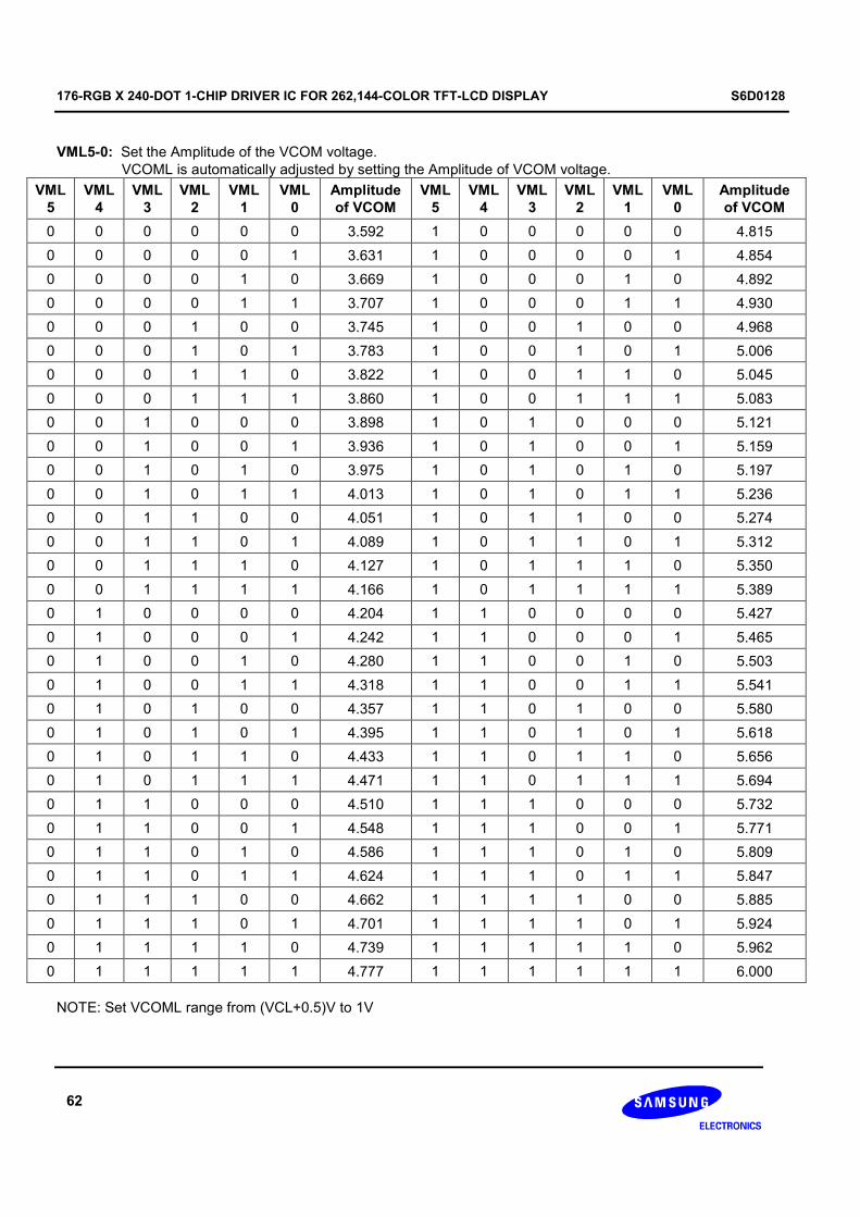
176-RGB X 240-DOT 1-CHIP DRIVER IC FOR 262,144-COLOR TFT-LCD DISPLAY S6D0128
62
VML5-0: Set the Amplitude of the VCOM voltage.
VCOML is automatically adjusted by setting the Amplitude of VCOM voltage.
VML
5
VML
4
VML
3
VML
2
VML
1
VML
0
Amplitude
of VCOM
VML
5
VML
4
VML
3
VML
2
VML
1
VML
0
Amplitude
of VCOM
0 0 0 0 0 0 3.592 1 0 0 0 0 0 4.815
0 0 0 0 0 1 3.631 1 0 0 0 0 1 4.854
0 0 0 0 1 0 3.669 1 0 0 0 1 0 4.892
0 0 0 0 1 1 3.707 1 0 0 0 1 1 4.930
0 0 0 1 0 0 3.745 1 0 0 1 0 0 4.968
0 0 0 1 0 1 3.783 1 0 0 1 0 1 5.006
0 0 0 1 1 0 3.822 1 0 0 1 1 0 5.045
0 0 0 1 1 1 3.860 1 0 0 1 1 1 5.083
0 0 1 0 0 0 3.898 1 0 1 0 0 0 5.121
0 0 1 0 0 1 3.936 1 0 1 0 0 1 5.159
0 0 1 0 1 0 3.975 1 0 1 0 1 0 5.197
0 0 1 0 1 1 4.013 1 0 1 0 1 1 5.236
0 0 1 1 0 0 4.051 1 0 1 1 0 0 5.274
0 0 1 1 0 1 4.089 1 0 1 1 0 1 5.312
0 0 1 1 1 0 4.127 1 0 1 1 1 0 5.350
0 0 1 1 1 1 4.166 1 0 1 1 1 1 5.389
0 1 0 0 0 0 4.204 1 1 0 0 0 0 5.427
0 1 0 0 0 1 4.242 1 1 0 0 0 1 5.465
0 1 0 0 1 0 4.280 1 1 0 0 1 0 5.503
0 1 0 0 1 1 4.318 1 1 0 0 1 1 5.541
0 1 0 1 0 0 4.357 1 1 0 1 0 0 5.580
0 1 0 1 0 1 4.395 1 1 0 1 0 1 5.618
0 1 0 1 1 0 4.433 1 1 0 1 1 0 5.656
0 1 0 1 1 1 4.471 1 1 0 1 1 1 5.694
0 1 1 0 0 0 4.510 1 1 1 0 0 0 5.732
0 1 1 0 0 1 4.548 1 1 1 0 0 1 5.771
0 1 1 0 1 0 4.586 1 1 1 0 1 0 5.809
0 1 1 0 1 1 4.624 1 1 1 0 1 1 5.847
0 1 1 1 0 0 4.662 1 1 1 1 0 0 5.885
0 1 1 1 0 1 4.701 1 1 1 1 0 1 5.924
0 1 1 1 1 0 4.739 1 1 1 1 1 0 5.962
0 1 1 1 1 1 4.777 1 1 1 1 1 1 6.000
NOTE: Set VCOML range from (VCL+0.5)V to 1V
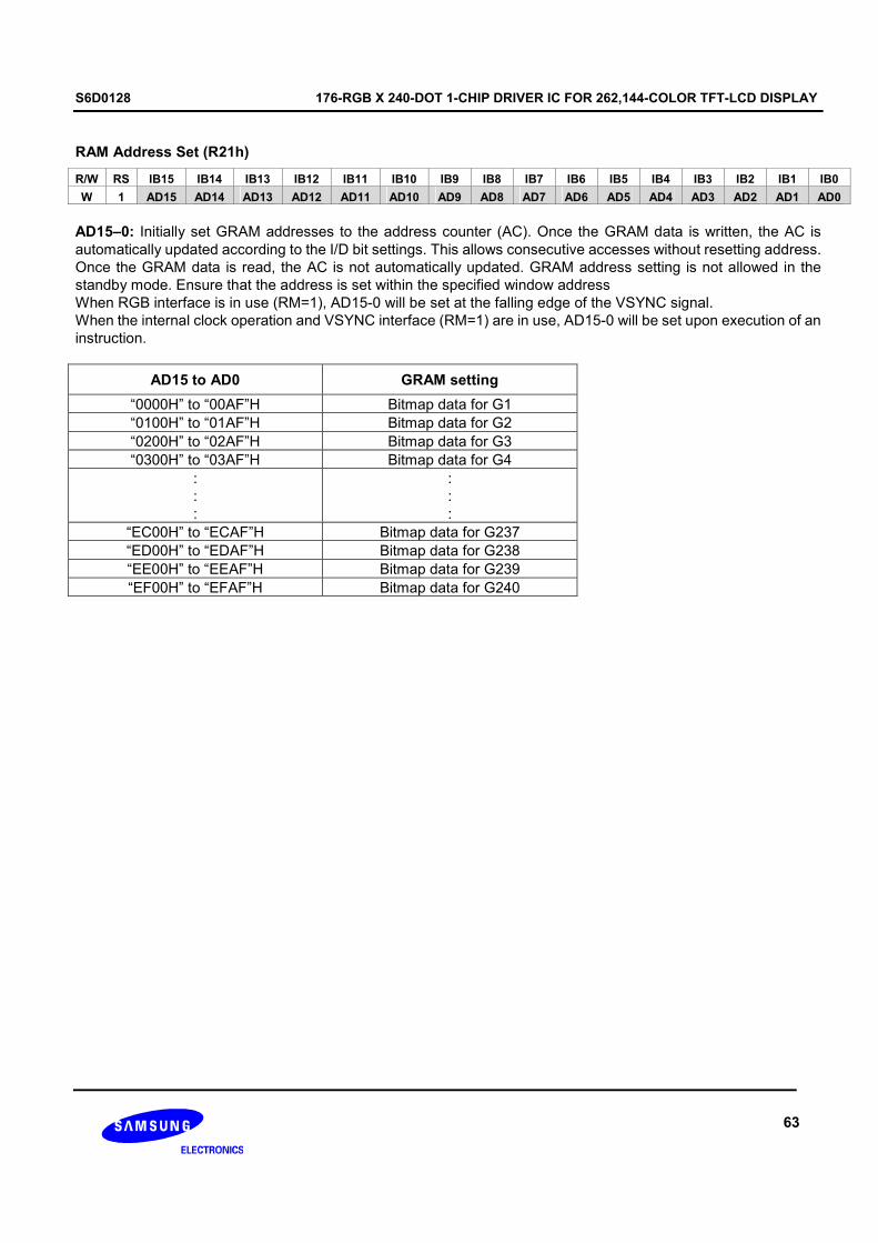
S6D0128 176-RGB X 240-DOT 1-CHIP DRIVER IC FOR 262,144-COLOR TFT-LCD DISPLAY
63
RAM Address Set (R21h)
R/W RS IB15 IB14 IB13 IB12 IB11 IB10 IB9 IB8 IB7 IB6 IB5 IB4 IB3 IB2 IB1 IB0
W 1 AD15 AD14 AD13 AD12 AD11 AD10 AD9 AD8 AD7 AD6 AD5 AD4 AD3 AD2 AD1 AD0
AD15–0: Initially set GRAM addresses to the address counter (AC). Once the GRAM data is written, the AC is
automatically updated according to the I/D bit settings. This allows consecutive accesses without resetting address.
Once the GRAM data is read, the AC is not automatically updated. GRAM address setting is not allowed in the
standby mode. Ensure that the address is set within the specified window address
When RGB interface is in use (RM=1), AD15-0 will be set at the falling edge of the VSYNC signal.
When the internal clock operation and VSYNC interface (RM=1) are in use, AD15-0 will be set upon execution of an
instruction.
AD15 to AD0 GRAM setting
“0000H” to “00AF”H Bitmap data for G1
“0100H” to “01AF”H Bitmap data for G2
“0200H” to “02AF”H Bitmap data for G3
“0300H” to “03AF”H Bitmap data for G4
:
:
:
:
:
:
“EC00H” to “ECAF”H Bitmap data for G237
“ED00H” to “EDAF”H Bitmap data for G238
“EE00H” to “EEAF”H Bitmap data for G239
“EF00H” to “EFAF”H Bitmap data for G240
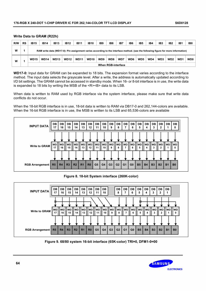
176-RGB X 240-DOT 1-CHIP DRIVER IC FOR 262,144-COLOR TFT-LCD DISPLAY S6D0128
64
Write Data to GRAM (R22h)
R/W RS IB15 IB14 IB13 IB12 IB11 IB10 IB9 IB8 IB7 IB6 IB5 IB4 IB3 IB2 IB1 IB0
W 1 RAM write data (WD17-0): Pin assignment varies according to the interface method. (see the following figure for more information)
WD15 WD14 WD13 WD12 WD11 WD10 WD9 WD8 WD7 WD6 WD5 WD4 WD3 WD2 WD1 WD0 W 1
When RGB-interface
WD17-0: Input data for GRAM can be expanded to 18 bits. The expansion format varies according to the interface
method. The input data selects the grayscale level. After a write, the address is automatically updated according to
I/D bit settings. The GRAM cannot be accessed in standby mode. When 16- or 8-bit interface is in use, the write data
is expanded to 18 bits by writing the MSB of the <R><B> data to its LSB.
When data is written to RAM used by RGB interface via the system interface, please make sure that write data
conflicts do not occur.
When the 18-bit RGB interface is in use, 18-bit data is written to RAM via DB17-0 and 262,144-colors are available.
When the 16-bit RGB interface is in use, the MSB is written to its LSB and 65,536-colors are available
INPUT DATA
R5 R4 R3 R2 R1 R0 G5 G4 G3 G2 G1 G0 B5 B4 B3 B2 B1 B0RGB Arrangement
WD
17
WD
16
WD
15
WD
14
WD
13
WD
12
WD
11
WD
10
WD
9
WD
8
WD
7
WD
6
WD
5
WD
4
WD
3
WD
2
WD
1
WD
0Write to GRAM
DB
17
DB
16
DB
15
DB
14
DB
13
DB
12
DB
11
DB
10
DB
9
DB
8
DB
7
DB
6
DB
5
DB
4
DB
3
DB
2
DB
1
DB
0
Figure 8. 18-bit System interface (260K-color)
INPUT DATA
R5 R4 R3 R2 R1 R0 G5 G4 G3 G2 G1 G0 B5 B4 B3 B2 B1 B0RGB Arrangement
WD
17
WD
16
WD
15
WD
14
WD
13
WD
12
WD
11
WD
10
WD
9
WD
8
WD
7
WD
6
WD
5
WD
4
WD
3
WD
2
WD
1
WD
0Write to GRAM
DB
17
DB
16
DB
15
DB
14
DB
13
DB
12
DB
11
DB
10
DB
8
DB
7
DB
6
DB
5
DB
4
DB
3
DB
2
DB
1
Figure 9. 68/80 system 16-bit interface (65K-color) TRI=0, DFM1-0=00

S6D0128 176-RGB X 240-DOT 1-CHIP DRIVER IC FOR 262,144-COLOR TFT-LCD DISPLAY
65
INPUT DATA
R5 R4 R3 R2 R1 R0 G5 G4 G3 G2 G1 G0 B5 B4 B3 B2 B1 B0RGB Arrangement
WD
17
WD
16
WD
15
WD
14
WD
13
WD
12
WD
11
WD
10
WD
9
WD
8
WD
7
WD
6
WD
5
WD
4
WD
3
WD
2
WD
1
WD
0Write to GRAM
DB
17
DB
16
DB
15
DB
14
DB
13
DB
12
DB
11
DB
10
DB
8
1st Transmission 2nd Transmission
DB
7
DB
6
DB
5
DB
4
DB
3
DB
2
DB
1
DB
17
DB
16
Figure 10. 80 system 16bit interface (260K-color) TRI=1, DFM1-0=10
INPUT DATA
R5 R4 R3 R2 R1 R0 G5 G4 G3 G2 G1 G0 B5 B4 B3 B2 B1 B0RGB Arrangement
WD
17
WD
16
WD
15
WD
14
WD
13
WD
12
WD
11
WD
10
WD
9
WD
8
WD
7
WD
6
WD
5
WD
4
WD
3
WD
2
WD
1
WD
0Write to GRAM
DB
2
DB
1
DB
17
DB
16
DB
15
DB
14
DB
13
DB
12
DB
11
1st Transmission 2nd Transmission
DB
10
DB
8
DB
7
DB
6
DB
5
DB
4
DB
3
DB
2
DB
1
Figure 11. 80 system 16bit interface (260K-color) TRI=1, DFM1-0=11
INPUT DATA
R5 R4 R3 R2 R1 R0 G5 G4 G3 G2 G1 G0 B5 B4 B3 B2 B1 B0RGB Arrangement
WD
17
WD
16
WD
15
WD
14
WD
13
WD
12
WD
11
WD
10
WD
9
WD
8
WD
7
WD
6
WD
5
WD
4
WD
3
WD
2
WD
1
WD
0Write to GRAM
DB
17
DB
16
DB
15
DB
14
DB
13
DB
12
DB
11
DB
10
DB
9
1st Transmission 2nd Transmission
DB
17
DB
16
DB
15
DB
14
DB
13
DB
12
DB
11
DB
10
DB
9
Figure 12. 9-bit System interface (260K-color)

176-RGB X 240-DOT 1-CHIP DRIVER IC FOR 262,144-COLOR TFT-LCD DISPLAY S6D0128
66
INPUT DATA
R5 R4 R3 R2 R1 R0 G5 G4 G3 G2 G1 G0 B5 B4 B3 B2 B1 B0RGB Arrangement
WD
17
WD
16
WD
15
WD
14
WD
13
WD
12
WD
11
WD
10
WD
9
WD
8
WD
7
WD
6
WD
5
WD
4
WD
3
WD
2
WD
1
WD
0Write to GRAM
1st Transmission 2nd Transmission
DB
17
DB
16
DB
15
DB
14
DB
13
DB
12
DB
11
DB
10
DB
17
DB
16
DB
15
DB
14
DB
13
DB
12
DB
11
DB
10
Figure 13. 68/80-system 8-bit interface (65K-color) TRI=0, DFM1-0=00
INPUT DATA
RGB Arrangement
WD
17
WD
16
WD
15
WD
14
WD
13
WD
12
WD
11
WD
10
WD
9
WD
8
WD
7
WD
6
WD
5
WD
4
WD
3
WD
2
WD
1
WD
0Write to GRAM
R5 R4 R3 R2 R1 R0 G5 G4 G3 G2 G1 G0 B5 B4 B3 B2 B1 B0
1st Transmission 2nd Transmission 3rd Transmission
DB
17
DB
16
DB
15
DB
14
DB
13
DB
12
DB
17
DB
16
DB
15
DB
14
DB
13
DB
12
DB
17
DB
16
DB
15
DB
14
DB
13
DB
12
Figure 14. 80-system 8-bit interface (260K-color) TRI=1, DFM1-0=10
Figure 15. 80-system 8-bit interface (65K-color) TRI=1, DFM1-0=11
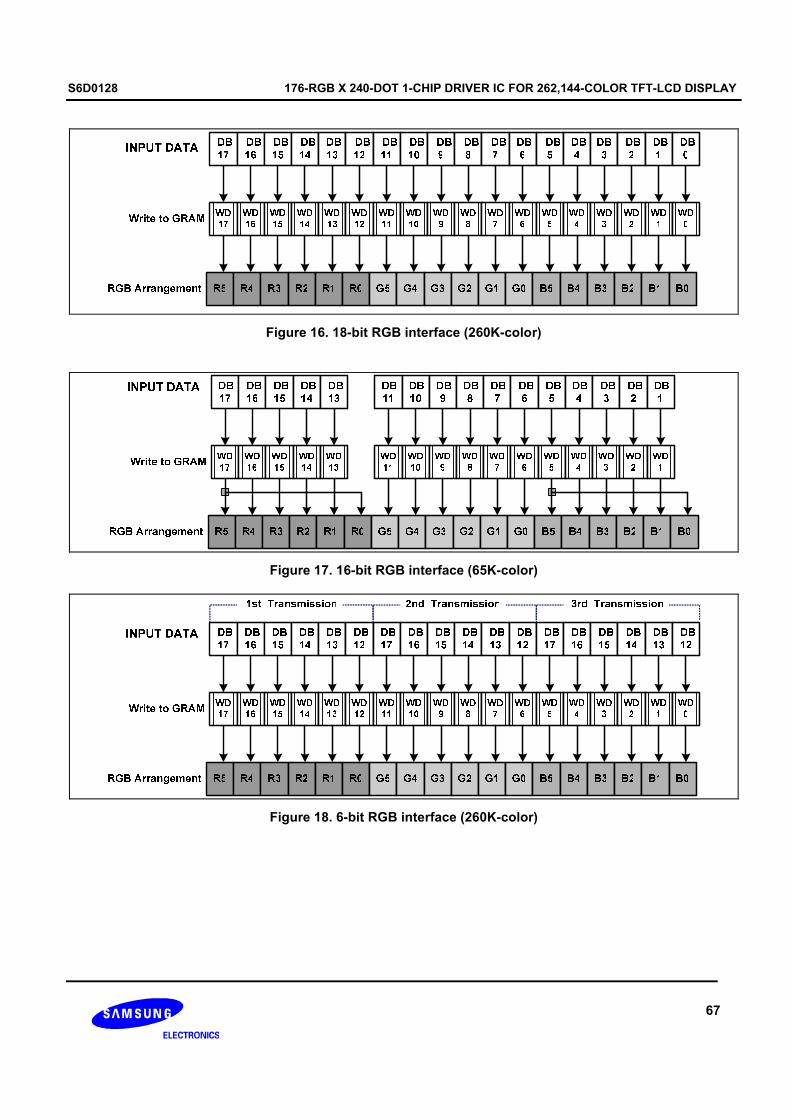
S6D0128 176-RGB X 240-DOT 1-CHIP DRIVER IC FOR 262,144-COLOR TFT-LCD DISPLAY
67
Figure 16. 18-bit RGB interface (260K-color)
Figure 17. 16-bit RGB interface (65K-color)
Figure 18. 6-bit RGB interface (260K-color)

176-RGB X 240-DOT 1-CHIP DRIVER IC FOR 262,144-COLOR TFT-LCD DISPLAY S6D0128
68
Figure 19. Memory data write sequence

S6D0128 176-RGB X 240-DOT 1-CHIP DRIVER IC FOR 262,144-COLOR TFT-LCD DISPLAY
69
RAM ACCESS via RGB INTERFACE & SYSTEM INTERFACE
All the data for display is written to the internal RAM in the S6D0128 when RGB interface is in use. In this method,
data, including that in both the motion picture area and the screen update frame, can only be transferred via RGB
interface. Data for display that is not in the motion picture area or the screen update frame can be written via the
system interface.
RAM can be accessed via the system interface when RGB interface is in use. When data is written to RAM during
RGB interface mode, the ENABLE bit should be low to stop data writing via RGB interface, because RAM writing is
always performed in synchronization with the DOTCLK input when ENABLE is high. After this RAM access via the
system interface, a waiting time is needed for a write/read bus cycle before the next RAM access starts via RGB
interface. When a RAM write conflict occurs, data writing is not guaranteed.
Figure 20. RAM access via RGB Interface & System Interface (EPL=1)
VSYNC
ENABLE
DOTCLK
DB17-0
Serial interface RM=0 Index
R22 Address set
Index R22
Writing display data except moving picture
display areaRM=0 Address
set Index R22
Moving picture display area
2001/01/01 00:00
Still picture display area
Writing moving picture display area
Writing moving picturedisplay area
Index set
Writing picture Writing picture
Writing still picture display area
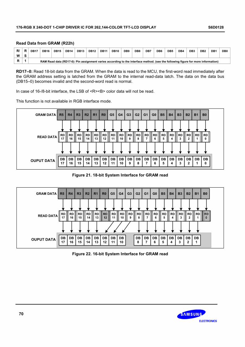
176-RGB X 240-DOT 1-CHIP DRIVER IC FOR 262,144-COLOR TFT-LCD DISPLAY S6D0128
70
Read Data from GRAM (R22h)
R/
W
R
S
DB17 DB16 DB15 DB14 DB13 DB12 DB11 DB10 DB9 DB8 DB7 DB6 DB5 DB4 DB3 DB2 DB1 DB0
R 1 RAM Read data (RD17-0): Pin assignment varies according to the interface method. (see the following figure for more information)
RD17–0: Read 18-bit data from the GRAM. When the data is read to the MCU, the first-word read immediately after
the GRAM address setting is latched from the GRAM to the internal read-data latch. The data on the data bus
(DB15–0) becomes invalid and the second-word read is normal.
In case of 16-/8-bit interface, the LSB of <R><B> color data will not be read.
This function is not available in RGB interface mode.
OUPUT DATA
R5 R4 R3 R2 R1 R0 G5 G4 G3 G2 G1 G0 B5 B4 B3 B2 B1 B0GRAM DATA
READ DATA
DB
17
DB
16
DB
15
DB
14
DB
13
DB
12
DB
11
DB
10
DB
9
DB
8
DB
7
DB
6
DB
5
DB
4
DB
3
DB
2
DB
1
DB
0
RD
17
RD
16
RD
15
RD
14
RD
13
RD
12
RD
11
RD
10
RD
9
RD
8
RD
7
RD
6
RD
5
RD
4
RD
3
RD
2
RD
1
RD
0
Figure 21. 18-bit System Interface for GRAM read
R5 R4 R3 R2 R1 R0 G5 G4 G3 G2 G1 G0 B5 B4 B3 B2 B1 B0
DB
17
DB
16
DB
15
DB
14
DB
13
DB
12
DB
11
DB
10
DB
8
DB
7
DB
6
DB
5
DB
4
DB
3
DB
2
DB
1
RD
17
RD
16
RD
15
RD
14
RD
13
RD
12
RD
11
RD
10
RD
9
RD
8
RD
7
RD
6
RD
5
RD
4
RD
3
RD
2
RD
1
RD
0
OUPUT DATA
GRAM DATA
READ DATA
Figure 22. 16-bit System Interface for GRAM read
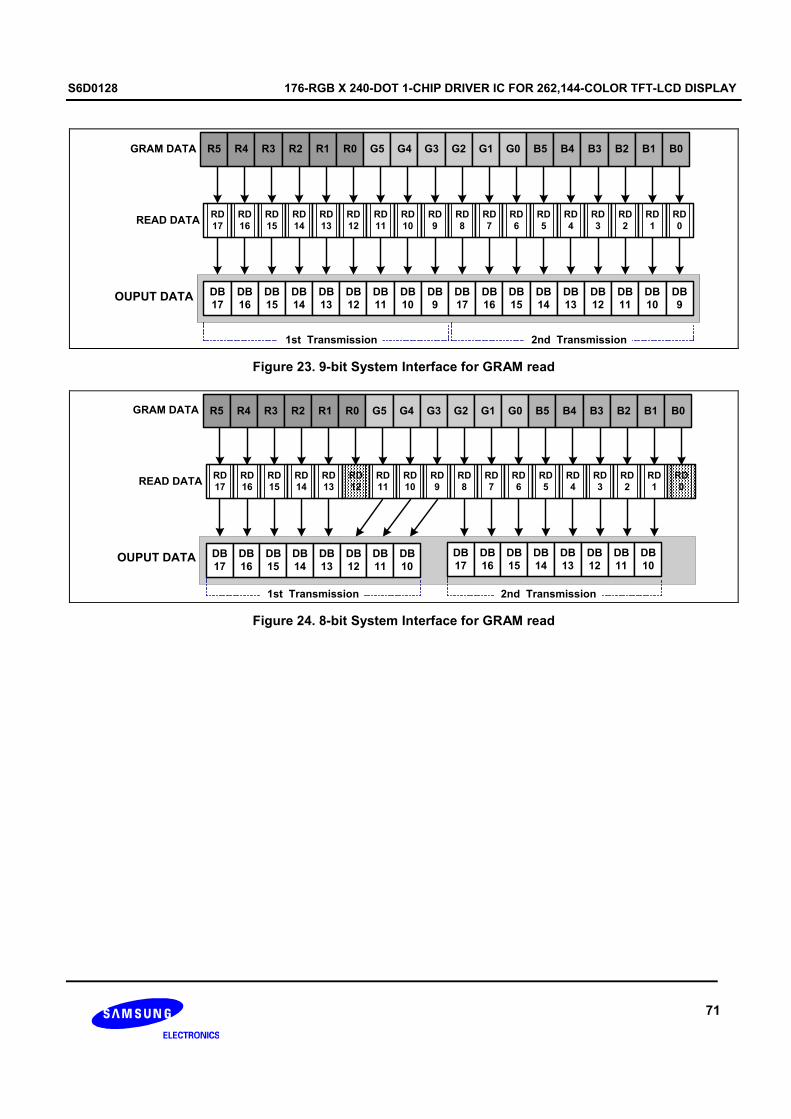
S6D0128 176-RGB X 240-DOT 1-CHIP DRIVER IC FOR 262,144-COLOR TFT-LCD DISPLAY
71
R5 R4 R3 R2 R1 R0 G5 G4 G3 G2 G1 G0 B5 B4 B3 B2 B1 B0
DB
17
DB
16
DB
15
DB
14
DB
13
DB
12
DB
11
DB
10
DB
9
1st Transmission 2nd Transmission
OUPUT DATA
GRAM DATA
READ DATARD
17
RD
16
RD
15
RD
14
RD
13
RD
12
RD
11
RD
10
RD
9
RD
8
RD
7
RD
6
RD
5
RD
4
RD
3
RD
2
RD
1
RD
0
DB
17
DB
16
DB
15
DB
14
DB
13
DB
12
DB
11
DB
10
DB
9
Figure 23. 9-bit System Interface for GRAM read
R5 R4 R3 R2 R1 R0 G5 G4 G3 G2 G1 G0 B5 B4 B3 B2 B1 B0
DB
17
DB
16
DB
15
DB
14
DB
13
DB
12
DB
11
DB
10
1st Transmission 2nd Transmission
OUPUT DATA
GRAM DATA
READ DATARD
17
RD
16
RD
15
RD
14
RD
13
RD
12
RD
11
RD
10
RD
9
RD
8
RD
7
RD
6
RD
5
RD
4
RD
3
RD
2
RD
1
RD
0
DB
17
DB
16
DB
15
DB
14
DB
13
DB
12
DB
11
DB
10
Figure 24. 8-bit System Interface for GRAM read

176-RGB X 240-DOT 1-CHIP DRIVER IC FOR 262,144-COLOR TFT-LCD DISPLAY S6D0128
72
End
Read More ?
Index Write (21h)
Yes
No
Index Write (22h)
18-/16- System Interface
Memory Address Write
Read Valid Data
Start
RM = 0
Read Dummy Data
End
Read More ?
Index Write (21h)
Yes
No
Index Write (22h)
9-/8- System Interface
Memory Address Write
Read Upper Word Valid DataRead Lower Word Valid Data
Start
RM = 0
Read Dummy Data 2 times
Figure 25. GRAM read sequence

S6D0128 176-RGB X 240-DOT 1-CHIP DRIVER IC FOR 262,144-COLOR TFT-LCD DISPLAY
73
Gamma Control (R30h to R39h)
R/W RS IB15 IB14 IB13 IB12 IB11 IB10 IB9 IB8 IB7 IB6 IB5 IB4 IB3 IB2 IB1 IB0
W 1 0 0 0 0 0 PKP
12
PKP
11
PKP
10 0 0 0 0 0
PKP
02
PKP
01
PKP
00
W 1 0 0 0 0 0 PKP
32
PKP
31
PKP
30 0 0 0 0 0
PKP
22
PKP
21
PKP
20
W 1 0 0 0 0 0 PKP
52
PKP
51
PKP
50 0 0 0 0 0
PKP
42
PKP
41
PKP
40
W 1 0 0 0 0 0 PRP
12
PRP
11
PRP
10 0 0 0 0 0
PRP
02
PRP
01
PRP
00
W 1 0 0 0 0 0 PKN
12
PKN
11
PKN
10 0 0 0 0 0
PKN
02
PKN
01
PKN
00
W 1 0 0 0 0 0 PKN
32
PKN
31
PKN
30 0 0 0 0 0
PKN
22
PKN
21
PKN
20
W 1 0 0 0 0 0 PKN
52
PKN
51
PKN
50 0 0 0 0 0
PKN
42
PKN
41
PKN
40
W 1 0 0 0 0 0 PRN
12
PRN
11
PRN
10 0 0 0 0 0
PRN
02
PRN
01
PRN
00
W 1 0 0 0 VRP
14
VRP
13
VRP
12
VRP
11
VRP
10 0 0 0 0
VRP
03
VRP
02
VRP
01
VRP
00
W 1 0 0 0 VRN
14
VRN
13
VRN
12
VRN
11
VRN
10 0 0 0 0
VRN
03
VRN
02
VRN
01
VRN
00
PKP52–00: The gamma micro adjustment register for the positive polarity output
PRP12-00: The gradient adjustment register for the positive polarity output
PKN52-00: The gamma micro adjustment register for the negative polarity output
PRN12-00: The gradient adjustment register for the negative polarity output
VRP14-10: The amplitude adjustment register for the positive polarity output
VRN14-10: The amplitude adjustment register for the negative polarity output
VRP03-00: The reference adjustment register for the positive polarity output
VRN03-00: The reference adjustment register for the negative polarity output
For details, see the GAMMA ADJUSTMENT FUNCTION.

176-RGB X 240-DOT 1-CHIP DRIVER IC FOR 262,144-COLOR TFT-LCD DISPLAY S6D0128
74
Gate Scan Position (R40h)
R/W RS IB15 IB14 IB13 IB12 IB11 IB10 IB9 IB8 IB7 IB6 IB5 IB4 IB3 IB2 IB1 IB0
W 1 0 0 0 0 0 0 0 0 0 0 0 SCN4 SCN3 SCN2 SCN1 SCN0
SCN 4-0: Set the scanning starting position of the gate driver.
Scanning start position SCN4 SCN3 SCN2 SCN1 SCN0
GS=0 GS=1
0 0 0 0 0 G1 G240
0 0 0 0 1 G9 G232
0 0 0 1 0 G17 G224
:
:
:
:
:
:
:
:
:
:
:
:
:
:
1 1 0 1 0 G209 G32
1 1 0 1 1 G217 G24
1 1 1 0 0 G225 G16
G1
G176
G177
G240
G1
G240G232
G56
G57
GS = 0
NL = 10101
SCN4-0 = 00000
GS = 0
NL = 10101
SCN4-0 = 00111
Note: When Setting NL and SCN , Have to keep the condition of
[(Number of LCD driver lines + Scanning start position) < 241]
Figure 26. Relationship between NL and SCN set up value

S6D0128 176-RGB X 240-DOT 1-CHIP DRIVER IC FOR 262,144-COLOR TFT-LCD DISPLAY
75
Vertical Scroll Control (R41h)
R/W RS IB15 IB14 IB13 IB12 IB11 IB10 IB9 IB8 IB7 IB6 IB5 IB4 IB3 IB2 IB1 IB0
W 1 0 0 0 0 0 0 0 0 VL7 VL6 VL5 VL4 VL3 VL2 VL1 VL0
VL7-0: Specify scroll length at the scroll display for vertical smooth scrolling. Any raster-row from the 1st to 240
th can
be scrolled for the number of the raster-row. After 239th raster-row is displayed, the display restarts from the first
raster-row. The display-start raster-row (VL7-0) is valid when VLE1 = 1 or VLE2 = 1. The raster-row display is fixed
when VLE2-1 = 00.
VL7 VL6 VL5 VL4 VL3 VL2 VL1 VL0 Scroll length
0 0 0 0 0 0 0 0 0 raster-row
0 0 0 0 0 0 0 1 1 raster-row
0 0 0 0 0 0 1 0 2 raster-row
.
.
.
.
.
.
.
.
1 1 1 0 1 1 1 0 238 raster-row
1 1 1 0 1 1 1 1 239 raster-row
Note: Don’t set any higher raster-row than 239 (“EF”H)
1st
Screen Driving Position (R42h)
2nd
Screen Driving Position (R43h)
R/W RS IB15 IB14 IB13 IB12 IB11 IB10 IB9 IB8 IB7 IB6 IB5 IB4 IB3 IB2 IB1 IB0
W 1 SE17 SE16 SE15 SE14 SE13 SE12 SE11 SE10 SS17 SS16 SS15 SS14 SS13 SS12 SS11 SS10
W 1 SE27 SE26 SE25 SE24 SE23 SE22 SE21 SE20 SS27 SS26 SS25 SS24 SS23 SS22 SS21 SS20
SE17–10: Specify the driving end position for the first screen in a line unit. The LCD driving is performed to the 'set
value + 1' gate driver. For instance, when SS17–10 = 07h and SE17–10 = 10h are set, the LCD driving is performed
from G8 to G17, and non-display driving is performed for G1 to G7, G18, and others. Ensure that SS17–10
≤ SE17–10 ≤ AFh. For details, see the SCREEN-DIVISION DRIVING FUNCTION section.
SS17–10: Specify the drive starting position for the first screen in a line unit. The LCD driving starts from the ‘set
value +1’ gate driver.
SE27–20: Specify the driving end position for the second screen in a line unit. The LCD driving is performed to the
'set value + 1' gate driver. For instance, when SPT = 1, SS27–20 = 20h, and SE27–20 = AFh are set, the LCD
driving is performed from G33 to G80. Ensure that SS17–10 ≤ SE17–10 ≤ SS27–20 ≤ SE27–20 ≤ AFh. For details,
see the SCREEN-DIVISION DRIVING FUNCTION section.
SS27–20: Specify the driving start position for the second screen in a line unit. The LCD driving starts from the
'set value + 1' gate driver. The second screen is driven when SPT = 1.

176-RGB X 240-DOT 1-CHIP DRIVER IC FOR 262,144-COLOR TFT-LCD DISPLAY S6D0128
76
Horizontal RAM Address Position (R44h)
Vertical RAM Address Position (R45h)
R/W RS IB15 IB14 IB13 IB12 IB11 IB10 IB9 IB8 IB7 IB6 IB5 IB4 IB3 IB2 IB1 IB0
W 1 HEA
7
HEA
6
HEA
5
HEA
4
HEA
3
HEA
2
HEA
1
HEA
0
HSA
7
HSA
6
HSA
5
HSA
4
HSA
3
HSA
2
HSA
1
HSA
0
W 1 VEA
7
VEA
6
VEA
5
VEA
4
VEA
3
VEA
2
VEA
1
VEA
0
VSA
7
VSA
6
VSA
5
VSA
4
VSA
3
VSA
2
VSA
1
VSA
0
HSA7-0/HEA7-0: Specify the horizontal start/end positions of a window for access in memory. Data can be written
to the GRAM from the address specified by HSA7-0 to the address specified by HEA 7-0. Note that an address must
be set before RAM is written. Ensure 00h ≤ HSA7-0 ≤ HEA7-0 ≤ AFh.
VSA7-0/VEA7-0: Specify the vertical start/end positions of a window for access in memory. Data can be written to
the GRAM from the address specified by VSA7-0 to the address specified by VEA7-0. Note that an address must be
set before RAM is written. Ensure 00h ≤ VSA7-0 ≤ VEA7-0 ≤ EFh.
Window address
0000 H
EFAFH
HSA HEA
VSA
VEA
GRAM address space
Window address setting range
“ 00 ” h ≤ HSA7-0 ≤ HEA7-0 ≤ “ AF ” h “ 00 ” h ≤ VSA7-0 ≤ VEA7-0 ≤ “ EF ” h
NOTE: 1. Ensure that the window address area is within the GRAM address space
Figure 27. Window address setting range

S6D0128 176-RGB X 240-DOT 1-CHIP DRIVER IC FOR 262,144-COLOR TFT-LCD DISPLAY
77
RESET FUNCTION
The S6D0128 is internally initialized by RESET input. The reset input must be held for at least 1 ms. Do not access
the GRAM nor initially set the instructions until the R-C oscillation frequency is stable after power has been supplied
(10 ms).
Instruction Set Initialization
1. Start oscillation executed
2. Driver output control (NL4–0 = 11101, SS = 0, GS = 0, SM = 0, EPL=0, VSPL=0, HSPL=0, DPL=0)
3. LCD driving AC control (B/C = 0, EOR = 0)
4. Entry mode set (TRI = 0, DFM1-0 = 00, I/D1-0 = 11: Increment by 1, BGR=0)
5. Display control 1 (PT1-0 = 00, VLE2–1 = 00: No vertical scroll, SPT = 0, GON = 0, CL = 0: 260K-color mode, REV
= 0, D1–0 = 00: Display off)
6. Display control 2 (FP3-0 = 1000, BP3-0 = 1000)
7. Frame cycle control (NO1-0 = 00, SDT1-0 = 00, ECS1-0 = 00: no charge sharing, DIV1-0 = 00: 1-divided clock,
RTN3-0 = 0000: 16 clock cycle in 1H period)
8. External display interface (RIM1-0=00:18-bit RGB interface, DM1-0=00: operated by internal clock, RM=0:
system interface)
9. Power control 1 (SAP2-0 = 000, BT3-0 = 1111, DC2–0 = 011, SLP = 0, STB = 0: Standby mode off)
10. Power control 2 (GVD5-0 = 000000, VC2-0 = 000)
11. Power control 3 (PON = 0, PON1 = 0, AON = 0)
12. Power control 4 (VCMR = 0, VCM5-0 = 000000, VML5-0 = 000000)
13. RAM address set (AD15–0 = 0000h)
14. Gamma control
(PKP02–00 = 000, PKP12–10 = 000, PKP22–20 = 000, PKP32–30 = 000,
PK42–40 = 000, PKP52–50 = 000, PRP02–00 = 000, PRP12–10 = 000)
(PKN02–00 = 000, PKN12–10 = 000, PKN22–20 = 000, PKN32–30 = 000,
PKN42–40 = 000, PKN52–50 = 000, PRN02–00 = 000, PRN12–10 = 000)
VRP14–00 = 00000, VRP03–00 = 0000, VRN14–00 = 00000, VRN03–00 = 0000)
15. Gate scanning starting position (SCN4-0 = 00000)
16. Vertical scroll (VL7–0 = 0000000)
17. 1st screen division (SE17-10 = 11111111, SS17-10 = 00000000)
18. 2nd screen division (SE27-20 = 11111111, SS27-20 = 00000000)
19. Horizontal RAM address position (HEA7-0 = 10101111, HSA7-0 = 00000000)
20. Vertical RAM address position (VEA7-0 = 11101111, VSA7-0 = 00000000)
GRAM Data Initialization
GRAM is not automatically initialized by reset input but must be initialized by software while display is off
(D1-0 = 00).
Output Pin Initialization
1. LCD driver output pins (Source output) : Output VSS level
(Gate output) : Output VGL level
2. Oscillator output pin (OSC2): Outputs oscillation sign
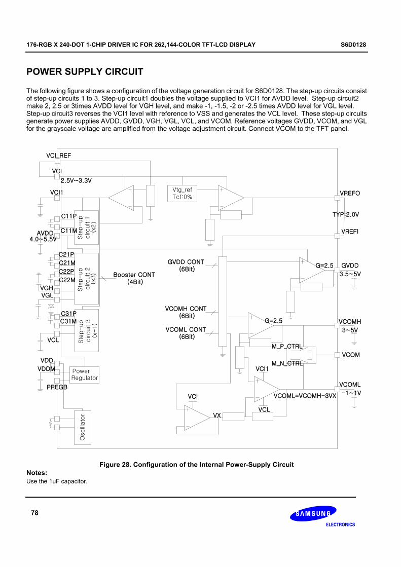
176-RGB X 240-DOT 1-CHIP DRIVER IC FOR 262,144-COLOR TFT-LCD DISPLAY S6D0128
78
POWER SUPPLY CIRCUIT
The following figure shows a configuration of the voltage generation circuit for S6D0128. The step-up circuits consist of step-up circuits 1 to 3. Step-up circuit1 doubles the voltage supplied to VCI1 for AVDD level. Step-up circuit2 make 2, 2.5 or 3times AVDD level for VGH level, and make -1, -1.5, -2 or -2.5 times AVDD level for VGL level. Step-up circuit3 reverses the VCI1 level with reference to VSS and generates the VCL level. These step-up circuits generate power supplies AVDD, GVDD, VGH, VGL, VCL, and VCOM. Reference voltages GVDD, VCOM, and VGL for the grayscale voltage are amplified from the voltage adjustment circuit. Connect VCOM to the TFT panel.
(x2
Ste
p-up
circuit 1
(x3)
Ste
p-up
circuit 2
PowerRegulator
(x-1)
Ste
p-up
circuit 3
Oscill
ato
r
Vtg_refTcf:0%
VCI1
VCI
VCL
G=2.5
G=2.5 GVDD
3.5~5V
VCOMH
3~5V
VCOML
-1~1V
VREFO
VREFI
TYP:2.0V
M_P_CTRL
M_N_CTRL
VCOM
VCOML CONT (6Bit)
GVDD CONT (6Bit)
VCOMH CONT (6Bit)
Booster CONT (4Bit)
VCI
2.5V~3.3V
VCI1
C11P
C11MAVDD4.0~5.5V
C21P
C21M
C22P
C22M
VGHVGL
VDD
VDDM
PREGB
C31P
C31M
VCL
VX
VCOML=VCOMH-3VX
VCI_REF
)
Figure 28. Configuration of the Internal Power-Supply Circuit
Notes:
Use the 1uF capacitor.
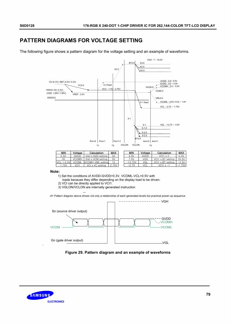
S6D0128 176-RGB X 240-DOT 1-CHIP DRIVER IC FOR 262,144-COLOR TFT-LCD DISPLAY
79
PATTERN DIAGRAMS FOR VOLTAGE SETTING
The following figure shows a pattern diagram for the voltage setting and an example of waveforms.
.
Note:1) Set the conditions of AVDD-GVDD>0.3V, VCOML-VCL>0.5V with
loads because they differ depending on the display load to be driven.2) VCI can be directly applied to VCI1.
VGH
GVDDVCOMH
VCOML
VGL
VCOM
Sn (source driver output)
Gn (gate driver output)
VCI & VCI_REF (2.5V~3.3V)
VDD3(1.8V~3.3V)
GND(0V)
VGH : 7 ~ 16.5V
VGL : -13.75 ~ -3.5V
VCL : -2.75 ~ -1.75V
VCOML : (VCL+0.5) ~ 1.0V
Pon=0 Pon=1 Pon1=1 Aon=0 Aon=1
VCI1 : 1.75 ~ 2.75V
X 2 fixed
X-1 fixed
X2.0
X2.5
X3.0
X-1
X-1.5
X-2.0
VC2-0
VREF : 2.0V
GVDD : 3.5 ~ 5.0V
VCOMH : 3.0 ~ 5.0V
AVDD : 4.0~ 5.5V
GVD5-0
VCM5-0
VML5-0
BT2-0
VGLON VCLON
X3.0
X-1
BT2-0
3) VGLON/VCLON are internally generated instruction
cf> Pattern diagram above shows not only a relationship of each generated levels but practical power-up sequence
T2T1 T3
X-2.5
MIN Voltage Calculation MAX3.5V GVDD Vref x GVD setting 5V3V VCOMH Vref x VCM setting 5V
VCL + 0.5V VCOML VCOMH-VML setting 1V1.75V VCI1 VCI x VC setting 2.75V
(VDD: 1.65V~1.95V)
MIN Voltage Calculation MAX4.0V AVDD VCI1 x 2 5.5V7.0V VGH VCI1 x BT setting 16.5V
-13.75V VGL VCI1 x BT setting -3.5V-2.75 VCL VCI1 x -1 -1.75V
Figure 29. Pattern diagram and an example of waveforms

176-RGB X 240-DOT 1-CHIP DRIVER IC FOR 262,144-COLOR TFT-LCD DISPLAY S6D0128
80
SET UP FLOW OF POWER
Apply the power in a sequence as shown in the following figure. The stable time of the oscillation circuit, step-up circuit, and operational amplifier depend on the external resistor or capacitance.
10ms or more
(Stable time of the
oscillation circuit)
External Power On
Sequence
Reset
After VDD is stable
1ms
Issues instructions for
power control (1)
Bits for power-supply
initial setting: VC2-0,
GVD5-0, VCM5-0,
VML5-0,(setting of the
source-driver grayscale
voltage)
Issues instruction for
power control(2)
Bits for power-supply
operation start setting: BT2-
0, DC2-0, Bits for source-
driver operational amplifier
operaton-start setting:
SAP2-0
Bits for step-up
circuit1 operation
start PON=1
Issues instruction for
power control(3)
Wait
(more than 1frame)
Instruction for
power control(1)
Bits for source-driver
operational amplifier
operation-stop setting:
SAP2-0
Instruction for
power control(2)
Bits for power supply
stop setting: AON
for operational
amplifier, DC2-0 for
step-up circuit
Display off Flow
Issues instruction for
other mode setting
Display-on Flow
10ms or more
(Stable times of step-
up circuit 1)50ms or more
(Stable time of the
step-up circuit 2 &
step-up circuit 3)
< Power-on Flow > < Power-off Flow >
Bits for step-up circuit2
& step-up circuit3
operation start PON1=1
Bits for amplifier circuit
operation start AON=140ms or more
(Stable time of the
step-up operational
amplifier)
External Power On
Sequence
AON off
more than 10ms
PON off
PON1 off
more than 10ms
Figure 30. Set up Flow of Power

S6D0128 176-RGB X 240-DOT 1-CHIP DRIVER IC FOR 262,144-COLOR TFT-LCD DISPLAY
81
EXTERNAL POWER ON / OFF SEQUENCE
a) EXTERNAL POWER ON SEQUENCE
VDD3 should reach 90% before VCI does so. When regulator cap is 1µF, RESETB must be applied after VCI
have been applied. The applied time gap between VCI and RESETB is minimum 1ms. As regulator cap becomes
larger, this time gap must be increased. Otherwise function is not guaranteed.
Figure 31. External power on sequence
b) EXTERNAL POWER OFF SEQUENCE
VCI should reach 90% before VDD3 does so. VCI must be powered down after RESETB have been powered
down. The time gap of powered down between RESETB and VCI is minimum 1ms. Otherwise function is not
guaranteed.
Figure 32. External power off sequence

176-RGB X 240-DOT 1-CHIP DRIVER IC FOR 262,144-COLOR TFT-LCD DISPLAY S6D0128
82
SET UP FLOW OF DISPLAY
Wait (more than 2 frame)
Display off
GON = 1
D1-0 = 10
<Display off flow> <Display on flow>
ECS2-0 = 000
Display off
GON = 0
D1-0 = 00
Display off
GON = 1
D1-0 = 10
Wait (more than 2 frame)
Display on
GON = 1
D1-0 = 11
Figure 33. Set up flow of display

S6D0128 176-RGB X 240-DOT 1-CHIP DRIVER IC FOR 262,144-COLOR TFT-LCD DISPLAY
83
< Standby> < Sleep>
Display off flow
Standby set (STB= 1 )
Oscillation start
Wait 10ms
Standby cancel (STB= 0 )
Power on flow
Display on flow
Display off flow
Sleep set (SLP= 1 )
Sleep cancel (SLP= 0 )
Display on flow
Standby set
Standby cancel
Sleep set
Sleep Cancel
Power on flow
Figure 34. Setup flow of Standby / Sleep
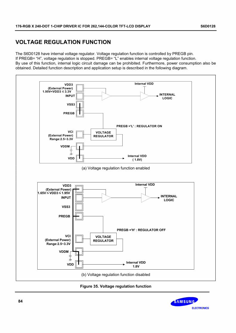
176-RGB X 240-DOT 1-CHIP DRIVER IC FOR 262,144-COLOR TFT-LCD DISPLAY S6D0128
84
VOLTAGE REGULATION FUNCTION
The S6D0128 have internal voltage regulator. Voltage regulation function is controlled by PREGB pin.
If PREGB= “H”, voltage regulation is stopped. PREGB= “L” enables internal voltage regulation function.
By use of this function, internal logic circuit damage can be prohibited. Furthermore, power consumption also be
obtained. Detailed function description and application setup is described in the following diagram.
VOLTAGE
REGULATOR
Internal VDD
( 1.8V)
VDD3
(External Power)
VDDM
PREGB
PREGB ='L' : REGULATOR ON
VDD
INPUT
Internal VDD
INTERNAL
LOGIC
VSS3
VCI
(External Power)
Range:2.5~3.3V
1.95V<VDD3≤3.3V
(a) Voltage regulation function enabled
VOLTAGE
REGULATOR
Internal VDD
1.8V
VDD3
(External Power)
VDDM
PREGB
PREGB ='H' : REGULATOR OFF
VDD
INPUT
Internal VDD
INTERNAL
LOGIC
VSS3
VCI
(External Power)
Range:2.5~3.3V
1.65V≤VDD3≤1.95V
(b) Voltage regulation function disabled
Figure 35. Voltage regulation function

S6D0128 176-RGB X 240-DOT 1-CHIP DRIVER IC FOR 262,144-COLOR TFT-LCD DISPLAY
85
INTERFACE SPECIFICATION
The S6D0128 incorporates a system interface, which is used to set instructions, and an external display interface,
which is used to display motion pictures. Selecting these interfaces to match the screen data (motion picture or still
picture) enables efficient transfer of data for display.
The external display interface includes RGB interface and VSYNC interface. This allows flicker-free screen update.
When RGB interface is selected, the synchronization signals (VSYNC, HSYNC, and DOTCLK) are available for use
in operating the display. The data for display (DB17-0) is written according to the values of the data enable signal
(ENABLE) in synchronization with the VSYNC, HSYNC, and DOTCLK signals. In addition, using the window
address function enables rewriting only to the internal RAM area to display motion pictures. Using this function also
enables simultaneously display of the motion picture area and the RAM data that was written.
The internal display operation is synchronized with the frame synchronization signal (VSYNC) in VSYNC interface
mode. When writing to the internal RAM is done within the required time after the falling edge of VSYNC, motion
pictures can be displayed via the conventional interface. There are some limitations on the timing and methods of
writing to RAM. See the section on the external display interface.
The S6D0128 has four operation modes for each display state. These settings are specified by control instructions
for external display interface. Transitions between modes should follow the transition flow.
Table 30. Display Operation Mode and RAM Access Selection
Operation Mode RAM Access Selection
(RM)
Display Operation Mode
(DM1-0)
Internal Clock Operation
(Displaying still picture)
System interface
(RM=0)
Internal clock operation
(DM1-0=00)
RGB interface (1)
(Displaying motion picture)
RGB interface
(RM=1)
RGB interface
(DM1-0=01)
RGB interface (2)
(Rewriting still picture while
displaying motion pictures)
System interface
(RM=0)
RGB interface
(DM1-0=01)
VSYNC interface
(Displaying motion Pictures)
System interface
(RM=0)
VSYNC interface
(DM1-0=10)
NOTES: 1) Instruction registers can only be set via system interface.
2) RGB interface and VSYNC interface cannot be used at the same time.
3) RGB interface mode cannot be set during operations.
4) For mode transitions, see the section on the external display interface.

176-RGB X 240-DOT 1-CHIP DRIVER IC FOR 262,144-COLOR TFT-LCD DISPLAY S6D0128
86
SYSTEM INTERFACE
S6D0128 is enabling to set instruction and access to RAM by selecting IM3/2/1/0 pin in the system interface mode.
Table 31. IM Bits and System Interface
IM3 IM2 IM1 IM0 System Interface DB Pin
0 0 0 0 68-system 16-bit interface DB17 to10, 8 to1
0 0 0 1 68-system 8-bit interface DB17 to10
0 0 1 0 80-system 16-bit interface DB17 to10, 8 to1
0 0 1 1 80-system 8-bit interface DB17 to10
0 1 0 * Serial peripheral interface (SPI) SDI / SDO
0 1 1 * Setting disabled -
1 0 0 0 68-system 18-bit interface DB17 to 0
1 0 0 1 68-system 9-bit interface DB17 to 9
1 0 1 0 80-system 18-bit interface DB17 to 0
1 0 1 1 80-system 9-bit interface DB17 to 9
1 1 * * Setting disabled -
68/80-SYSTEM 18-BIT BUS INTERFACE
Setting the IM3/2/1/0 (interface mode) to the VDD3/VSS/VSS/VSS level allows 68-system 18-bit parallel data
transfer. Setting the IM3/2/1/0 to the VDD3/VSS/VDD3/VSS level allows 80-system 18-bit parallel data transfer.
MPU
CSn
A1
/WR
/RD
D17-D0
CSB
RS
RW_WRB
E_RDB
DB17-DB0 18
S6D0128
Figure 36. Interface with the 18-bit Microcomputer
68/80-SYSTEM 18-bit interface data FORMAT
DB
17INPUT DATA
Instruction Bit
(IB)
DB
16
DB
15
DB
14
DB
13
DB
12
DB
11
DB
10
DB
9
DB
8
DB
7
DB
6
DB
5
DB
4
DB
3
DB
2
DB
1
DB
0
IB
15
IB
14
IB
13
IB
12
IB
11
IB
10
IB
9
IB
8
IB
7
IB
6
IB
5
IB
4
IB
3
IB
2
IB
1
IB
0
Figure 37. Instruction format for 18-bit Interface
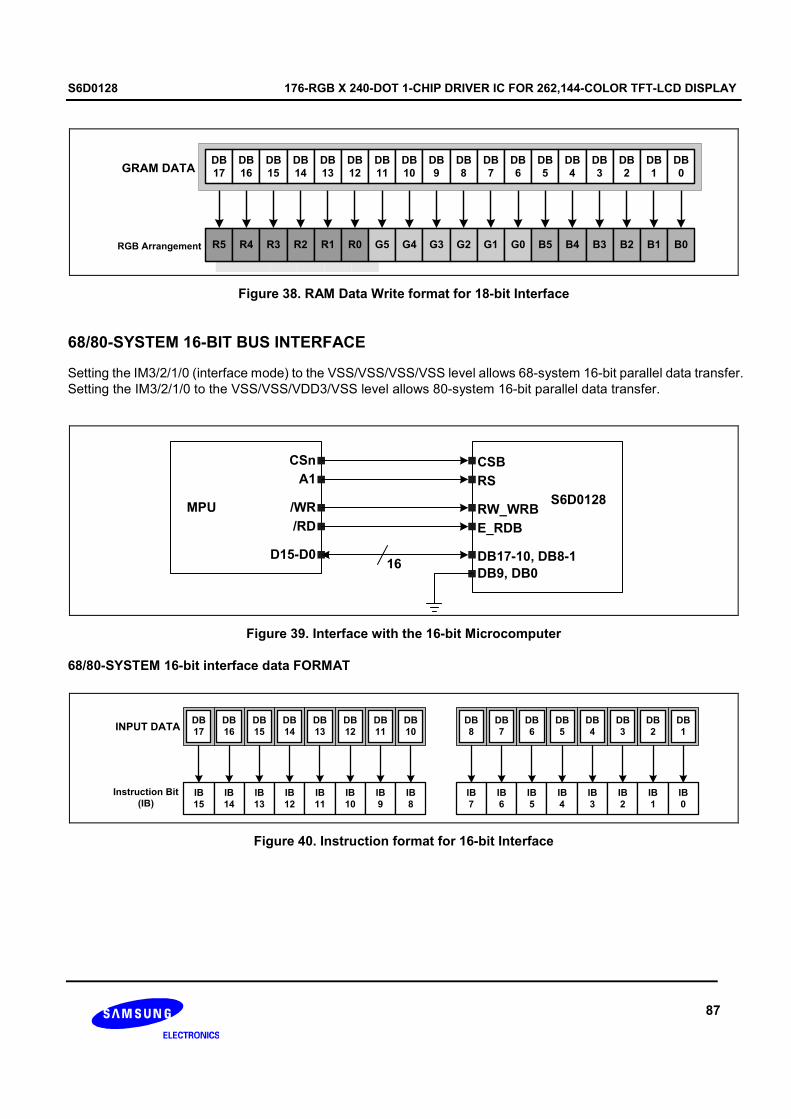
S6D0128 176-RGB X 240-DOT 1-CHIP DRIVER IC FOR 262,144-COLOR TFT-LCD DISPLAY
87
GRAM DATA
R5 R4 R3 R2 R1 R0 G5 G4 G3 G2 G1 G0 B5 B4 B3 B2 B1 B0RGB Arrangement
DB
17
DB
16
DB
15
DB
14
DB
13
DB
12
DB
11
DB
10
DB
9
DB
8
DB
7
DB
6
DB
5
DB
4
DB
3
DB
2
DB
1
DB
0
Figure 38. RAM Data Write format for 18-bit Interface
68/80-SYSTEM 16-BIT BUS INTERFACE
Setting the IM3/2/1/0 (interface mode) to the VSS/VSS/VSS/VSS level allows 68-system 16-bit parallel data transfer.
Setting the IM3/2/1/0 to the VSS/VSS/VDD3/VSS level allows 80-system 16-bit parallel data transfer.
MPU
CSn
A1
/WR
/RD
D15-D0
CSB
RS
RW_WRB
E_RDB
DB17-10, DB8-1 16
DB9, DB0
S6D0128
Figure 39. Interface with the 16-bit Microcomputer
68/80-SYSTEM 16-bit interface data FORMAT
DB
17INPUT DATA
Instruction Bit
(IB)
DB
16
DB
15
DB
14
DB
13
DB
12
DB
11
DB
10
DB
8
DB
7
DB
6
DB
5
DB
4
DB
3
DB
2
DB
1
IB
15
IB
14
IB
13
IB
12
IB
11
IB
10
IB
9
IB
8
IB
7
IB
6
IB
5
IB
4
IB
3
IB
2
IB
1
IB
0
Figure 40. Instruction format for 16-bit Interface

176-RGB X 240-DOT 1-CHIP DRIVER IC FOR 262,144-COLOR TFT-LCD DISPLAY S6D0128
88
DB
17
DB
16
DB
15
DB
14
DB
13
DB
12
DB
11
DB
10
DB
8
DB
7
DB
6
DB
5
DB
4
DB
3
DB
2
DB
1GRAM DATA
R5 R4 R3 R2 R1 R0 G5 G4 G3 G2 G1 G0 B5 B4 B3 B2 B1 B0RGB Arrangement
Figure 41. RAM Data Write format for 68/80 system 16-bit Interface (TRI=0, DFM1-0=00)
Figure 42. RAM Data Write format for 80system 16-bit Interface (TRI=1, DFM1-0=10)
Figure 43. RAM Data Write format for 80 system 16-bit Interface (TRI=1, DFM1-0=11)

S6D0128 176-RGB X 240-DOT 1-CHIP DRIVER IC FOR 262,144-COLOR TFT-LCD DISPLAY
89
68/80-SYSTEM 9-BIT BUS INTERFACE
Setting the IM3/2/1/0 (interface mode) to the VDD3/VSS/VSS/VDD3 level allows 68-system 9-bit parallel data
transfer using pins DB17–DB9. Setting the IM3/2/1/0 to be VDD3/VSS/VDD3/VDD3 level allows 80-system 9-bit
parallel data transfer. The 16-bit instructions and RAM data are divided into nine upper/lower bits and the transfer
starts from the upper nine bits. Fix unused pins DB8–DB0 to the VDD 3 or VSS level. Note that the upper bytes must
also be written when the index register is written.
MPU
CSn
A1
/WR
/RD
D8-D0
CSB
RS
RW_WRB
E_RDB
DB17-99
DB8-DB09
S6D0128
Figure 44. Interface to 9-bit Microcomputer
68/80-SYSTEM 9-bit interface data FORMAT
1st Transmission 2nd Transmission
DB
17INPUT DATA
Instruction Bit
(IB)
DB
16
DB
15
DB
14
DB
13
DB
12
DB
11
DB
10
DB
9
IB
15
IB
14
IB
13
IB
12
IB
11
IB
10
IB
9
IB
8
IB
7
IB
6
IB
5
IB
4
IB
3
IB
2
IB
1
IB
0
DB
17
DB
16
DB
15
DB
14
DB
13
DB
12
DB
11
DB
10
DB
9
Figure 45. Instruction format for 9-bit Interface
DB
17
DB
16
DB
15
DB
14
DB
13
DB
12
DB
11
DB
10
DB
9GRAM DATA
R5 R4 R3 R2 R1 R0 G5 G4 G3 G2 G1 G0 B5 B4 B3 B2 B1 B0RGB Arrangement
1st Transmission
DB
17
DB
16
DB
15
DB
14
DB
13
DB
12
DB
11
DB
10
DB
9
2nd Transmission
Figure 46. RAM Data Write format for 9-bit Interface
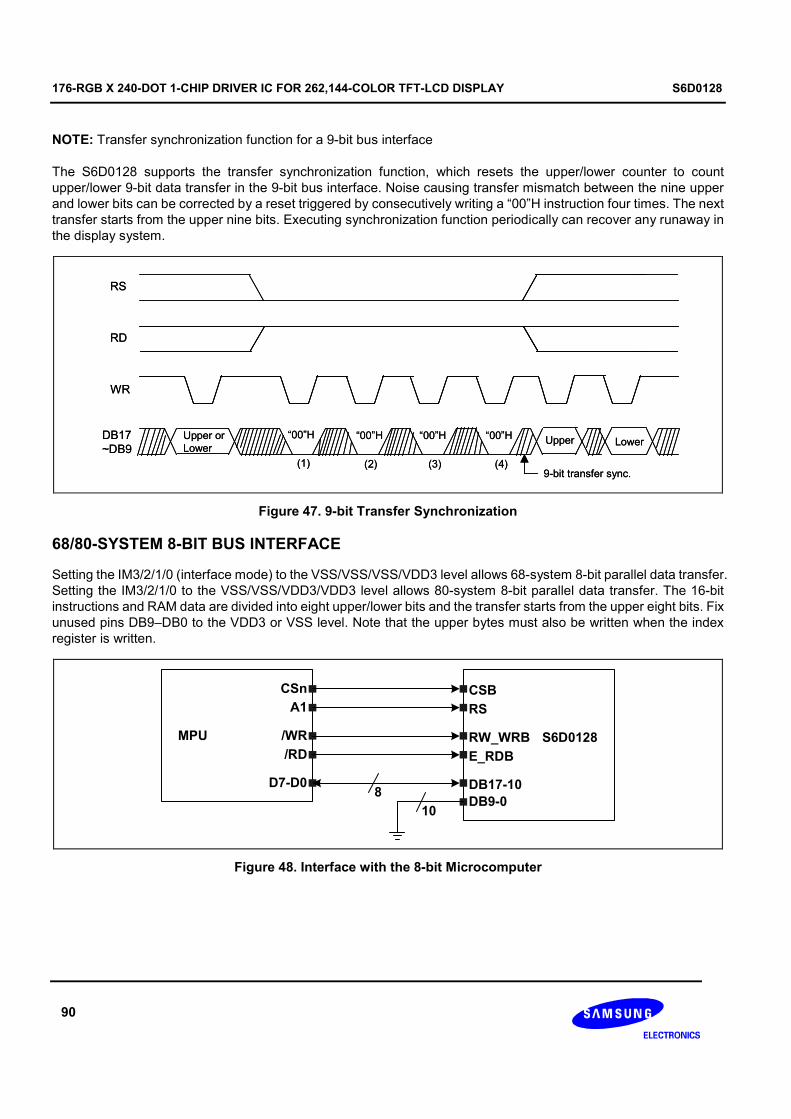
176-RGB X 240-DOT 1-CHIP DRIVER IC FOR 262,144-COLOR TFT-LCD DISPLAY S6D0128
90
NOTE: Transfer synchronization function for a 9-bit bus interface
The S6D0128 supports the transfer synchronization function, which resets the upper/lower counter to count
upper/lower 9-bit data transfer in the 9-bit bus interface. Noise causing transfer mismatch between the nine upper
and lower bits can be corrected by a reset triggered by consecutively writing a “00”H instruction four times. The next
transfer starts from the upper nine bits. Executing synchronization function periodically can recover any runaway in
the display system.
“00”H “00”H “00”H “00”HUpper or
LowerUpper Lower
RS
RD
WR
DB17
~DB9(1) (2) (3) (4)
9-bit transfer sync.
“00”H “00”H “00”H “00”HUpper or
LowerUpper Lower
RS
RD
WR
DB17
~DB9(1) (2) (3) (4)
9-bit transfer sync.
Figure 47. 9-bit Transfer Synchronization
68/80-SYSTEM 8-BIT BUS INTERFACE
Setting the IM3/2/1/0 (interface mode) to the VSS/VSS/VSS/VDD3 level allows 68-system 8-bit parallel data transfer.
Setting the IM3/2/1/0 to the VSS/VSS/VDD3/VDD3 level allows 80-system 8-bit parallel data transfer. The 16-bit
instructions and RAM data are divided into eight upper/lower bits and the transfer starts from the upper eight bits. Fix
unused pins DB9–DB0 to the VDD3 or VSS level. Note that the upper bytes must also be written when the index
register is written.
MPU
CSn
A1
/WR
/RD
D7-D0
CSB
RS
RW_WRB
E_RDB
DB17-108
DB9-010
S6D0128
Figure 48. Interface with the 8-bit Microcomputer
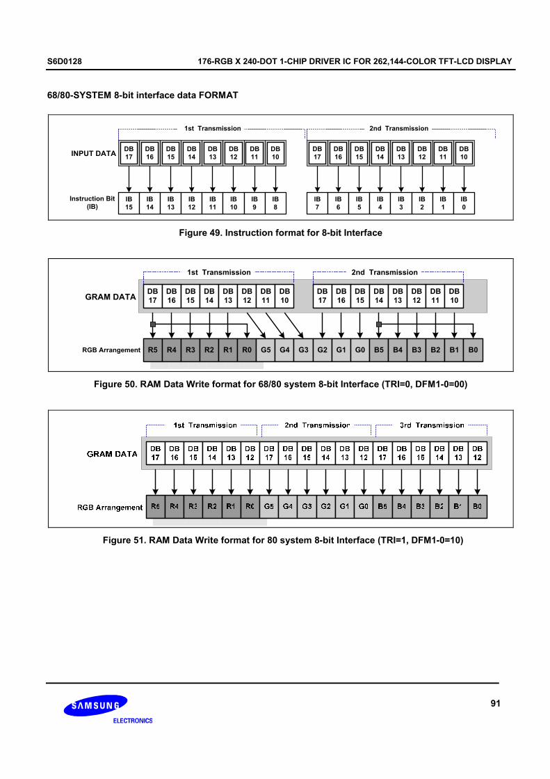
S6D0128 176-RGB X 240-DOT 1-CHIP DRIVER IC FOR 262,144-COLOR TFT-LCD DISPLAY
91
68/80-SYSTEM 8-bit interface data FORMAT
DB
17INPUT DATA
Instruction Bit
(IB)
DB
16
DB
15
DB
14
DB
13
DB
12
DB
11
DB
10
IB
15
IB
14
IB
13
IB
12
IB
11
IB
10
IB
9
IB
8
IB
7
IB
6
IB
5
IB
4
IB
3
IB
2
IB
1
IB
0
1st Transmission 2nd Transmission
DB
17
DB
16
DB
15
DB
14
DB
13
DB
12
DB
11
DB
10
Figure 49. Instruction format for 8-bit Interface
DB
17
DB
16
DB
15
DB
14
DB
13
DB
12
DB
11
DB
10
DB
17
DB
16
DB
15
DB
14
DB
13
DB
12
DB
11
DB
10GRAM DATA
R5 R4 R3 R2 R1 R0 G5 G4 G3 G2 G1 G0 B5 B4 B3 B2 B1 B0RGB Arrangement
1st Transmission 2nd Transmission
Figure 50. RAM Data Write format for 68/80 system 8-bit Interface (TRI=0, DFM1-0=00)
Figure 51. RAM Data Write format for 80 system 8-bit Interface (TRI=1, DFM1-0=10)

176-RGB X 240-DOT 1-CHIP DRIVER IC FOR 262,144-COLOR TFT-LCD DISPLAY S6D0128
92
Figure 52. RAM Data Write format for 80 system 8-bit Interface (TRI=1, DFM1-0=11)
NOTE: Transfer synchronization function for an 8-bit bus interface
The S6D0128 supports the transfer synchronization function, which resets the upper/lower counter to count
upper/lower 8-bit data transfer in the 8-bit bus interface. Noise causing transfer mismatch between the eight upper
and lower bits can be corrected by a reset triggered by consecutively writing a “00”H instruction four times. The next
transfer starts from the upper eight bits. Executing synchronization function periodically can recover any runaway in
the display system
“00”H “00”H “00”H “00”HUpper or
LowerUpper Lower
RS
RD
WR
DB17
~DB10(1) (2) (3) (4)
8-bit transfer sync.
“00”H “00”H “00”H “00”HUpper or
LowerUpper Lower
RS
RD
WR
DB17
~DB10(1) (2) (3) (4)
8-bit transfer sync.
Figure 53. 8-bit Transfer Synchronization

S6D0128 176-RGB X 240-DOT 1-CHIP DRIVER IC FOR 262,144-COLOR TFT-LCD DISPLAY
93
SERIAL DATA TRANSFER
Setting the IM3 pin to the VSS level allows serial peripheral interface (SPI) transfer, using the chip select line (CS*),
serial transfer clock line (SCL), serial input data (SDI), and serial output data (SDO). For a serial interface, the
IM0/ID pin function uses an ID pin. If the chip is set up for serial interface, the DB17-0 pins that are not used must be
fixed at VDD3 or VSS.
The S6D0128 initiates serial data transfer by transferring the start byte at the falling edge of CSB input. It ends serial
data transfer at the rising edge of CSB input.
The S6D0128 is selected when the 6-bit chip address in the start byte matches the 6-bit device identification code
that is assigned to the S6D0128. When selected, the S6D0128 receives the subsequent data string. The LSB of the
identification code can be determined by the ID pin. The five upper bits must be 01110. Two different chip addresses
must be assigned to a single S6D0128 because the seventh bit of the start byte is used as a register select bit (RS):
that is, when RS = 0, data can be written to the index register or status can be read, and when RS = 1, an instruction
can be issued or data can be written to or read from RAM. Read or write is selected according to the eighth bit of the
start byte (R/W bit). The data is received when the R/W bit is 0, and is transmitted when the R/W bit is 1.
After receiving the start byte, the S6D0128 receives or transmits the subsequent data byte-by-byte. The data is
transferred with the MSB first. All S6D0128 instructions are 16 bits. Two bytes are received with the MSB first (DB17
to 0), then the instructions are internally executed. After the start byte has been received, the first byte is fetched as
the upper eight bits of the instruction and the second byte is fetched as the lower eight bits of the instruction.
Four bytes of RAM read data after the start byte are invalid. The S6D0128 starts to read correct RAM data from the
fifth byte.
Table 32. Start Byte Format
Transfer bit S 1 2 3 4 5 6 7 8
Device ID code RS R/W Start byte format Transfer start
0 1 1 1 0 ID
NOTE: ID bit is selected by the IM0/ID pin.
Table 33. RS and R/W Bit Function
RS RW Function
0 0 Set index register
0 1 Read status
1 0 Writes instruction or RAM data
1 1 Reads instruction or RAM data
DB
17INPUT DATA
Instruction Bit
(IB)
DB
16
DB
15
DB
14
DB
13
DB
12
DB
11
DB
10
DB
8
DB
7
DB
6
DB
5
DB
4
DB
3
DB
2
DB
1
IB
15
IB
14
IB
13
IB
12
IB
11
IB
10
IB
9
IB
8
IB
7
IB
6
IB
5
IB
4
IB
3
IB
2
IB
1
IB
0
Figure 54. Instruction format for Serial Data Transfer
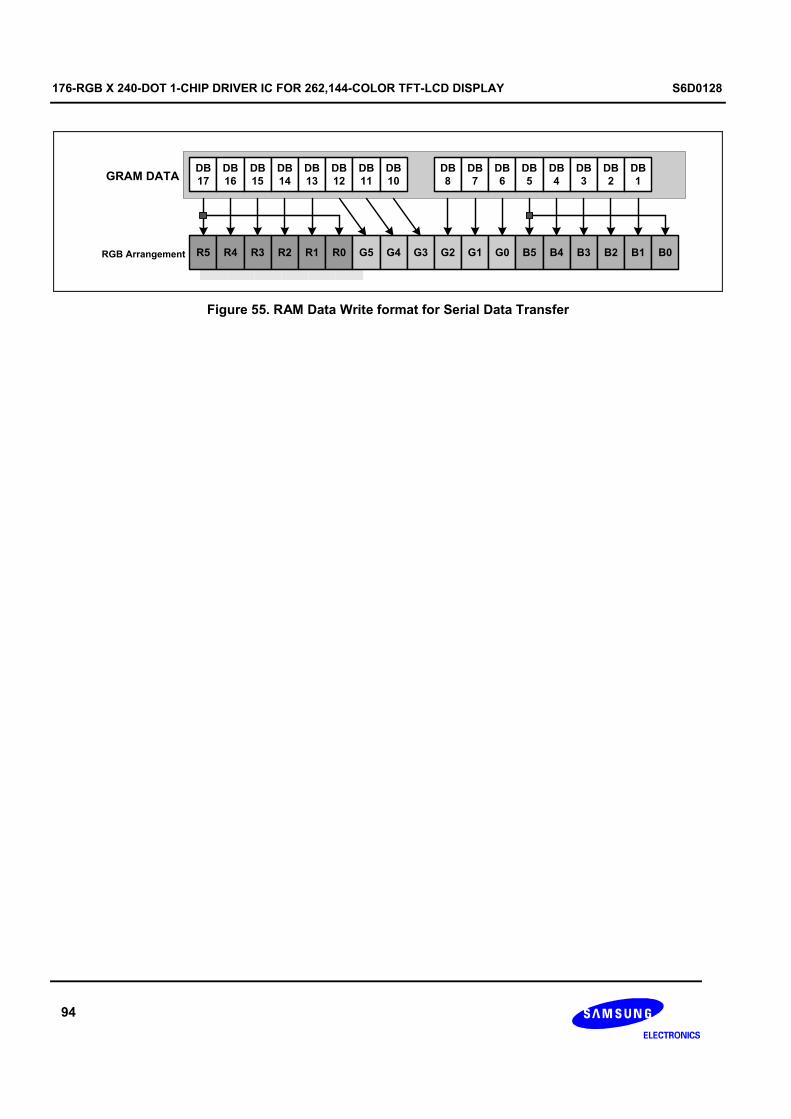
176-RGB X 240-DOT 1-CHIP DRIVER IC FOR 262,144-COLOR TFT-LCD DISPLAY S6D0128
94
DB
17
DB
16
DB
15
DB
14
DB
13
DB
12
DB
11
DB
10
DB
8
DB
7
DB
6
DB
5
DB
4
DB
3
DB
2
DB
1GRAM DATA
R5 R4 R3 R2 R1 R0 G5 G4 G3 G2 G1 G0 B5 B4 B3 B2 B1 B0RGB Arrangement
Figure 55. RAM Data Write format for Serial Data Transfer
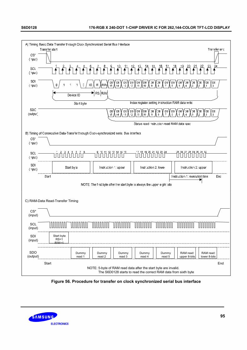
S6D0128 176-RGB X 240-DOT 1-CHIP DRIVER IC FOR 262,144-COLOR TFT-LCD DISPLAY
95
Figure 56. Procedure for transfer on clock synchronized serial bus interface
C) RAM-Data Read-Transfer Timing
Start byte RS=1 R/W=1
Dummy read 1
Dummy read 2
Dummy read 3
Dummy read 4
Dummy read 5
RAM read: upper 8-bits
RAM read: lower 8-bits
Start End NOTE: 5-byte of RAM read data after the start byte are invalid. The S6D0128 starts to read the correct RAM data from sixth byte
SCL (input)
SDI (input)
SDO(output)
CS*(input)

176-RGB X 240-DOT 1-CHIP DRIVER IC FOR 262,144-COLOR TFT-LCD DISPLAY S6D0128
96
CS*(input)
Start byteRS=1R/W=1
SDI(input)
Dummyread 1
Status readupper 8-bit
Status readlower 8-bit
Start End
NOTE: 2-byte of the RAM read after the start byte is invalid. The S6D0128 starts to read the correct RAM data from the third data.
D) Status Read/Instruction Read
SDO
(output)
Figure 57. Procedure for transfer on clock synchronized serial bus interface (continued)

S6D0128 176-RGB X 240-DOT 1-CHIP DRIVER IC FOR 262,144-COLOR TFT-LCD DISPLAY
97
VSYNC INTERFACE
The S6D0128 incorporates VSYNC interface, which enables motion pictures to be displayed with only the
conventional system interface and the frame synchronization signal (VSYNC). This interface requires minimal
changes from the conventional system to display motion pictures.
LCDC
VSYNC
DB17-10, 8-116
RS
CSB
RW_WRB
DB9, DB02
S6D0128
Figure 58. VSYNC Interface (example: 16bit interface)
When DM1-0=”10” and RM=”0”, VSYNC interface is available. In this interface the internal display operation is
synchronized with VSYNC. Data for display is written to RAM via the system interface with higher speed than for
internal display operation. This method enables flicker-free display of motion pictures with the conventional
interface.
Display operation can be achieved by using the internal clock generated by the internal oscillator and the VSYNC
input. Because all the data for display is written to RAM, only the data to be rewritten is transferred. This method
reduces the amount of data transferred during motion picture display operation.
Figure 59. Motion Picture Data Transfer via VSYNC Interface
VSYNC interface requires taking the minimum speed for RAM writing via the system interface and the frequency of
the internal clock into consideration. RAM writing should be performed with higher speed than the result obtained
from the calculation shown below. The internal memory write address counter is reset by VSYNC. So, ensure
interval time between VSYNC falling and GRAM data writing. The minimum interval time is 2 raster rows, and hence
the data writing should start only after that duration.

176-RGB X 240-DOT 1-CHIP DRIVER IC FOR 262,144-COLOR TFT-LCD DISPLAY S6D0128
98
-------------------------------------------------------------------------------------------------------------------------------------------------------
Internal clock frequency (fosc) [Hz] = Frame freq. × (Display raster-row (NL) + Front porch (FP) + Back porch (BP))
× 16-Clock × Fluctuation
Minimum speed for RAM writing [Hz] > 176 × Display raster-row (NL)
/ ((Back porch (BP) + Display raster-row (NL) – Margin) × 16 Clock) / fosc
NOTE: When RAM writing does not start immediately after the falling edge of VSYNC, the time between the falling edge of VSYNC and the RAM
writing start timing must also be considered.
-------------------------------------------------------------------------------------------------------------------------------------------------------
An example is shown below.
Example
Display size 176RGB × 240 raster-rows
Display line number 240 raster-row (NL=11101)
Back/Front porch 14 lines/2 lines (BP=1110/FP=0010)
Frame Frequency 60Hz
Internal clock frequency (fosc) [Hz] = 60 Hz × (240 + 2 + 14) lines× 16 clock × 1.1 / 0.9 = 300 kHz
NOTES: 1. Calculating the internal clock frequency requires considering the fluctuation. In the above case a 10%
Fluctuation within the VSYNC period is assumed.
2. The fluctuation includes LSI production variation and air temperature fluctuation. Other fluctuations,
including those for the external resistors and the supplied power, are not included in this example. Please keep in mind that a
margin for these factors is also needed.
Minimum speed for RAM writing [Hz] > 176 × 240 / ((14 + 240 – 2) lines × 16 clock) / 300 kHz = 3.14 MHz
NOTES: 3. In this case RAM writing starts immediately after the falling edge of VSYNC.
4. The margin for display raster-row should be two raster-rows or more at the completion of RAM writing
for one frame.
Therefore, when RAM writing starting immediately after the falling edge of VSYNC is performed at 3.14 MHz or more,
the data for display can be rewritten before display operation starts. This means that flicker-free display operation is
achieved.
Display
(240-line)
Back porch (14-line)
Front porch (2-line)
RAM write
Displaying
operation
VSYNC [Line]
240
0
executed
line
4.22 13.41
13.55 16.74 (60 Hz)
Back porch 14H
VSYNC
RAM write(10MHz) 42240 times
RAM write 3.15MHz
Displaying operation
RC oscillation ±10%
Displaying
operation
Figure 60. Operation for VSYNC Interface

S6D0128 176-RGB X 240-DOT 1-CHIP DRIVER IC FOR 262,144-COLOR TFT-LCD DISPLAY
99
Usage on VSYNC interface
1. The Example above is a calculated value. Please keep in mind that a margin for these factors is also
needed. Because production variation of the internal oscillator requires consideration.
2. The Example above is a calculated value of rewriting the whole screen. A limitation of the motion picture
area generates a margin for the RAM write speed.
(20- line)
(20- line)
Moving picture display (200-line)
Example: moving picture display area(20~220-line)
Back porch (14-line)
Front porch (2-line)
RAM write
[Line] 240
0
executed line
16.74 (60 Hz)
[ms]
Back porch 14H
VSYNC
RAM write 3.15MH
Displaying
operation
RC oscillation ±10 Displaying
operation
220
11.17 13.52
20
Figure 61. Limitation of Motion picture Area
3. During the period between the completion of displaying one frame data and the next VSYNC signal, the
display will remain front porch period.
4. Transition between the internal operating clock mode (DM1-0=”00”) and VSYNC interface mode will be
valid after the completion of the screen, which is displayed when the instruction is set.

176-RGB X 240-DOT 1-CHIP DRIVER IC FOR 262,144-COLOR TFT-LCD DISPLAY S6D0128
100
Address setting
VSYNC interface mode setting
(DM1-0=10, RM=0)
Index register setting(R22h)
Wait more than 1 frame
VSYNC interface
RAM data writing
VSYNC interface
Operation
Internal clock mode setting
(DM1-0=00, RM=0)
Wait more than 1 frame
Internal clock operation
Internal clock operation
Display operation in
synchronization with
the internal clock
The value set in DM1-
0 and RM will be valid
after completion of 1-
frame display.
Display operation in
synchronization with
VSYNC
Note: When the interface mode is switched,
VSYNC should be input before setting
DM1-0 and RM bit.
Internal clock operation =>VSYNC interface
Wait more than 1 frame
Internal clock mode setting
(DM1-0=00, RM=0)
Internal clock operation
VSYNC interface operationDisplay operation in
synchronization with
VSYNC
The value set in DM1-
0 and RM will be valid
after completion of 1-
frame display.
Display operation in
synchronization with
the internal clock
Note: When switching to internal clock mode,
Please keep supplying VSYNC signal for
more than 1 frame.
VSYNC interface => Internal clock operation
Figure 62. Transition between the Internal Operating Clock Mode and VSYNC Interface Mode
5. Partial display and vertical scroll functions are not available on VSYNC interface mode.
6. The VSYNC interface is performed by the method above.
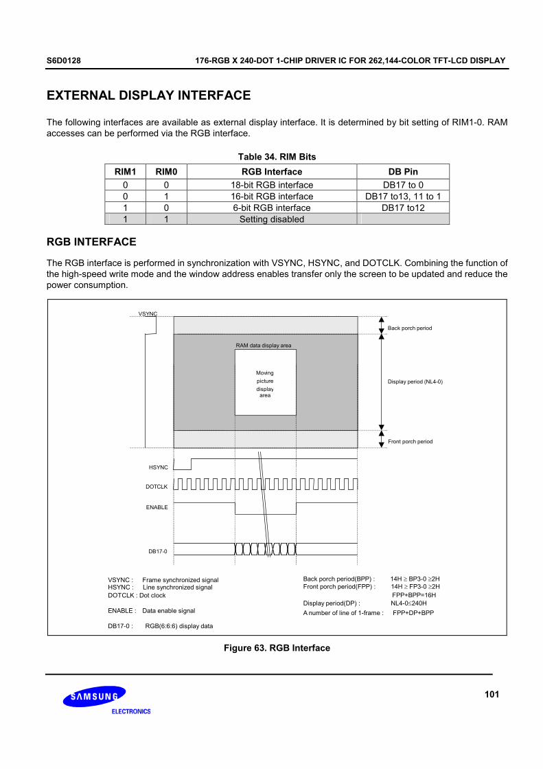
S6D0128 176-RGB X 240-DOT 1-CHIP DRIVER IC FOR 262,144-COLOR TFT-LCD DISPLAY
101
EXTERNAL DISPLAY INTERFACE
The following interfaces are available as external display interface. It is determined by bit setting of RIM1-0. RAM
accesses can be performed via the RGB interface.
Table 34. RIM Bits
RIM1 RIM0 RGB Interface DB Pin
0 0 18-bit RGB interface DB17 to 0
0 1 16-bit RGB interface DB17 to13, 11 to 1
1 0 6-bit RGB interface DB17 to12
1 1 Setting disabled
RGB INTERFACE
The RGB interface is performed in synchronization with VSYNC, HSYNC, and DOTCLK. Combining the function of
the high-speed write mode and the window address enables transfer only the screen to be updated and reduce the
power consumption.
Moving picture display area
Moving
picture
displayarea
RAM data display area
VSYNC
Back porch period
Front porch period
Display period (NL4-0)
HSYNC
DOTCLK
ENABLE
DB17-0
VSYNC : Frame synchronized signal HSYNC : Line synchronized signal DOTCLK : Dot clock
ENABLE : Data enable signal
DB17-0 : RGB(6:6:6) display data
Back porch period(BPP) : 14H ≥ BP3-0 ≥2H Front porch period(FPP) : 14H ≥ FP3-0 ≥2H
Display period(DP) : NL4-0≤240H
A number of line of 1-frame : FPP+DP+BPP
FPP+BPP=16H
Figure 63. RGB Interface
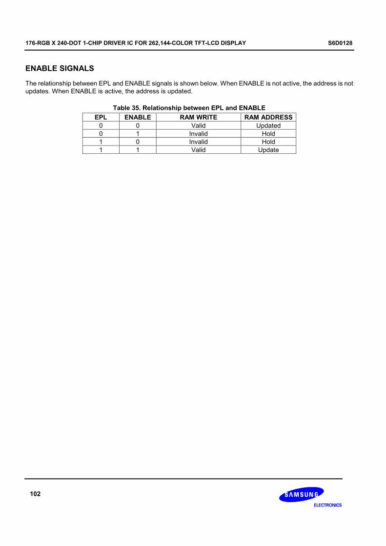
176-RGB X 240-DOT 1-CHIP DRIVER IC FOR 262,144-COLOR TFT-LCD DISPLAY S6D0128
102
ENABLE SIGNALS
The relationship between EPL and ENABLE signals is shown below. When ENABLE is not active, the address is not
updates. When ENABLE is active, the address is updated.
Table 35. Relationship between EPL and ENABLE
EPL ENABLE RAM WRITE RAM ADDRESS
0 0 Valid Updated
0 1 Invalid Hold
1 0 Invalid Hold
1 1 Valid Update

S6D0128 176-RGB X 240-DOT 1-CHIP DRIVER IC FOR 262,144-COLOR TFT-LCD DISPLAY
103
RGB INTERFACE TIMING
Time chart for RGB interface is shown below. (In case of EPL = 0)
Figure 64. 16-/18-bit RGB Interface Timing (In case of EPL = 0, DPL = 0, VSPL = 0, HSPL = 0)
VLW: The period in which VSYNC is “Low” level
HLW: The period in which HSYNC is “Low” level
DTST: Set up time of data transfer
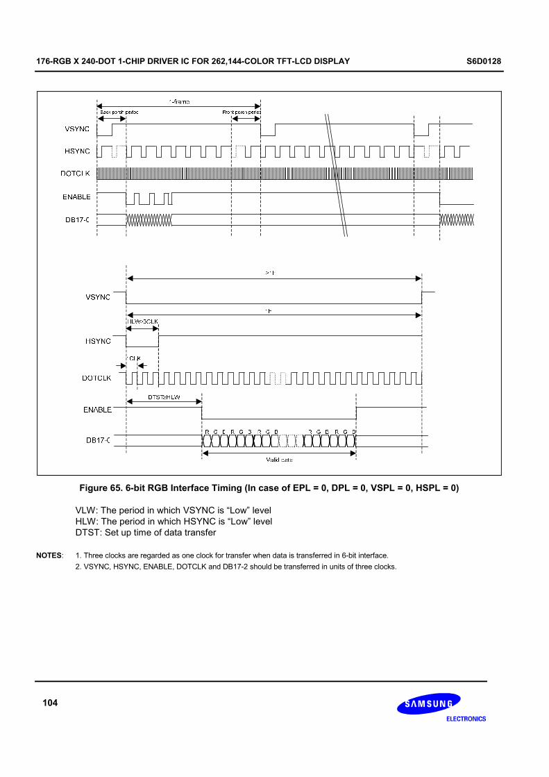
176-RGB X 240-DOT 1-CHIP DRIVER IC FOR 262,144-COLOR TFT-LCD DISPLAY S6D0128
104
Figure 65. 6-bit RGB Interface Timing (In case of EPL = 0, DPL = 0, VSPL = 0, HSPL = 0)
VLW: The period in which VSYNC is “Low” level
HLW: The period in which HSYNC is “Low” level
DTST: Set up time of data transfer
NOTES: 1. Three clocks are regarded as one clock for transfer when data is transferred in 6-bit interface.
2. VSYNC, HSYNC, ENABLE, DOTCLK and DB17-2 should be transferred in units of three clocks.
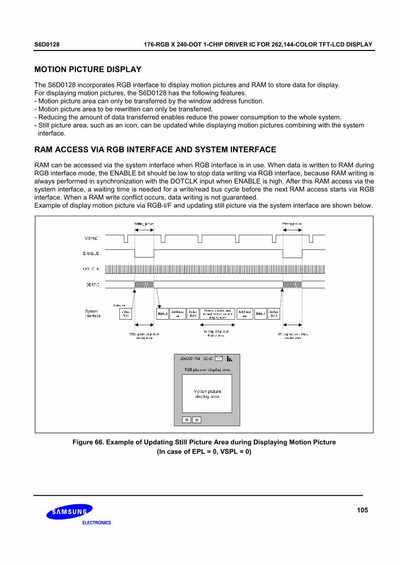
S6D0128 176-RGB X 240-DOT 1-CHIP DRIVER IC FOR 262,144-COLOR TFT-LCD DISPLAY
105
MOTION PICTURE DISPLAY
The S6D0128 incorporates RGB interface to display motion pictures and RAM to store data for display.
For displaying motion pictures, the S6D0128 has the following features.
- Motion picture area can only be transferred by the window address function.
- Motion picture area to be rewritten can only be transferred.
- Reducing the amount of data transferred enables reduce the power consumption to the whole system.
- Still picture area, such as an icon, can be updated while displaying motion pictures combining with the system
interface.
RAM ACCESS VIA RGB INTERFACE AND SYSTEM INTERFACE
RAM can be accessed via the system interface when RGB interface is in use. When data is written to RAM during
RGB interface mode, the ENABLE bit should be low to stop data writing via RGB interface, because RAM writing is
always performed in synchronization with the DOTCLK input when ENABLE is high. After this RAM access via the
system interface, a waiting time is needed for a write/read bus cycle before the next RAM access starts via RGB
interface. When a RAM write conflict occurs, data writing is not guaranteed.
Example of display motion picture via RGB-I/F and updating still picture via the system interface are shown below.
Figure 66. Example of Updating Still Picture Area during Displaying Motion Picture
(In case of EPL = 0, VSPL = 0)
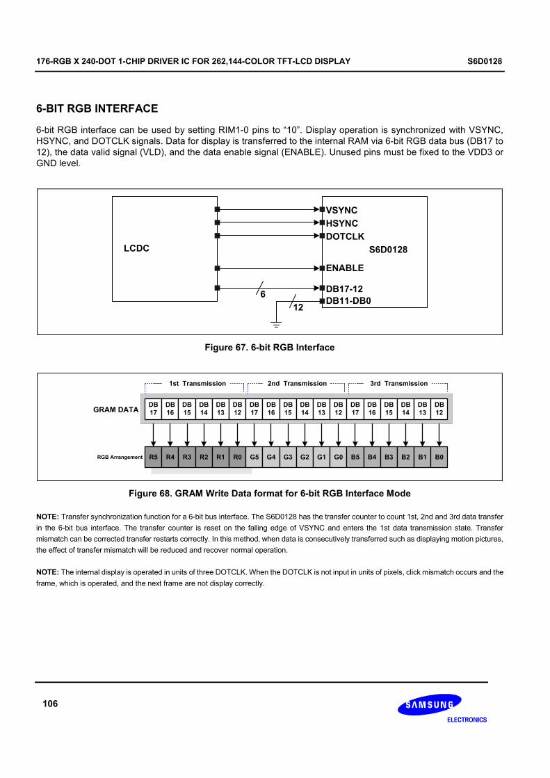
176-RGB X 240-DOT 1-CHIP DRIVER IC FOR 262,144-COLOR TFT-LCD DISPLAY S6D0128
106
6-BIT RGB INTERFACE
6-bit RGB interface can be used by setting RIM1-0 pins to “10”. Display operation is synchronized with VSYNC,
HSYNC, and DOTCLK signals. Data for display is transferred to the internal RAM via 6-bit RGB data bus (DB17 to
12), the data valid signal (VLD), and the data enable signal (ENABLE). Unused pins must be fixed to the VDD3 or
GND level.
LCDC
VSYNC
HSYNC
DOTCLK
ENABLE
DB17-12
DB11-DB06
12
S6D0128
Figure 67. 6-bit RGB Interface
DB
17
DB
16
DB
15
DB
14
DB
13
DB
12GRAM DATA
R5 R4 R3 R2 R1 R0 G5 G4 G3 G2 G1 G0 B5 B4 B3 B2 B1 B0RGB Arrangement
1st Transmission 2nd Transmission 3rd Transmission
DB
17
DB
16
DB
15
DB
14
DB
13
DB
12
DB
17
DB
16
DB
15
DB
14
DB
13
DB
12
Figure 68. GRAM Write Data format for 6-bit RGB Interface Mode
NOTE: Transfer synchronization function for a 6-bit bus interface. The S6D0128 has the transfer counter to count 1st, 2nd and 3rd data transfer
in the 6-bit bus interface. The transfer counter is reset on the falling edge of VSYNC and enters the 1st data transmission state. Transfer
mismatch can be corrected transfer restarts correctly. In this method, when data is consecutively transferred such as displaying motion pictures,
the effect of transfer mismatch will be reduced and recover normal operation.
NOTE: The internal display is operated in units of three DOTCLK. When the DOTCLK is not input in units of pixels, click mismatch occurs and the
frame, which is operated, and the next frame are not display correctly.

S6D0128 176-RGB X 240-DOT 1-CHIP DRIVER IC FOR 262,144-COLOR TFT-LCD DISPLAY
107
Figure 69. Transfer Synchronization Function when 6-bit RGB Interface
16-BIT RGB INTERFACE
16-bit RGB interface can be used by setting RIM1-0 pins to 01. Display operation is synchronized with VSYNC,
HSYNC, and DOTCLK signals. Data for display is transferred to the internal RAM via 6-bit RGB data bus (DB17-13
and 11-1). Instruction should be set via the system interface.
LCDC
VSYNC
HSYNC
DOTCLK
ENABLE
DB17-13, DB11-1
DB12, DB016
2
S6D0128
Figure 70. 16-bit RGB Interface to System
DB
17
DB
16
DB
15
DB
14
DB
13
DB
9
DB
11
DB
10
DB
8
DB
7
DB
6
DB
5
DB
4
DB
3
DB
2
DB
1GRAM DATA
R5 R4 R3 R2 R1 R0 G5 G4 G3 G2 G1 G0 B5 B4 B3 B2 B1 B0RGB Arrangement
Figure 71. GRAM Write Data in the 16-bit RGB Interface Mode
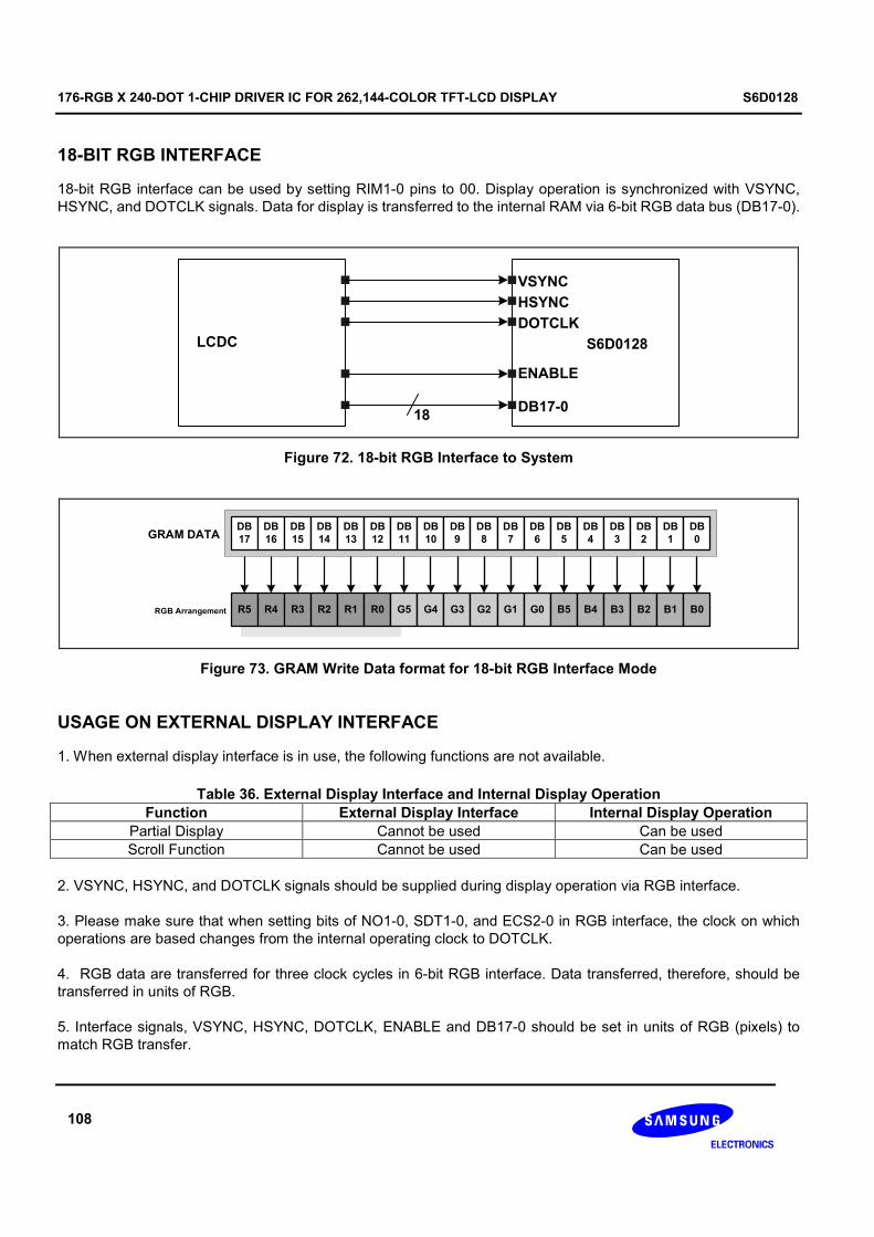
176-RGB X 240-DOT 1-CHIP DRIVER IC FOR 262,144-COLOR TFT-LCD DISPLAY S6D0128
108
18-BIT RGB INTERFACE
18-bit RGB interface can be used by setting RIM1-0 pins to 00. Display operation is synchronized with VSYNC,
HSYNC, and DOTCLK signals. Data for display is transferred to the internal RAM via 6-bit RGB data bus (DB17-0).
LCDC
VSYNC
HSYNC
DOTCLK
ENABLE
DB17-018
S6D0128
Figure 72. 18-bit RGB Interface to System
GRAM DATA
R5 R4 R3 R2 R1 R0 G5 G4 G3 G2 G1 G0 B5 B4 B3 B2 B1 B0RGB Arrangement
DB
17
DB
16
DB
15
DB
14
DB
13
DB
12
DB
11
DB
10
DB
9
DB
8
DB
7
DB
6
DB
5
DB
4
DB
3
DB
2
DB
1
DB
0
Figure 73. GRAM Write Data format for 18-bit RGB Interface Mode
USAGE ON EXTERNAL DISPLAY INTERFACE
1. When external display interface is in use, the following functions are not available.
Table 36. External Display Interface and Internal Display Operation
Function External Display Interface Internal Display Operation
Partial Display Cannot be used Can be used
Scroll Function Cannot be used Can be used
2. VSYNC, HSYNC, and DOTCLK signals should be supplied during display operation via RGB interface.
3. Please make sure that when setting bits of NO1-0, SDT1-0, and ECS2-0 in RGB interface, the clock on which
operations are based changes from the internal operating clock to DOTCLK.
4. RGB data are transferred for three clock cycles in 6-bit RGB interface. Data transferred, therefore, should be
transferred in units of RGB.
5. Interface signals, VSYNC, HSYNC, DOTCLK, ENABLE and DB17-0 should be set in units of RGB (pixels) to
match RGB transfer.
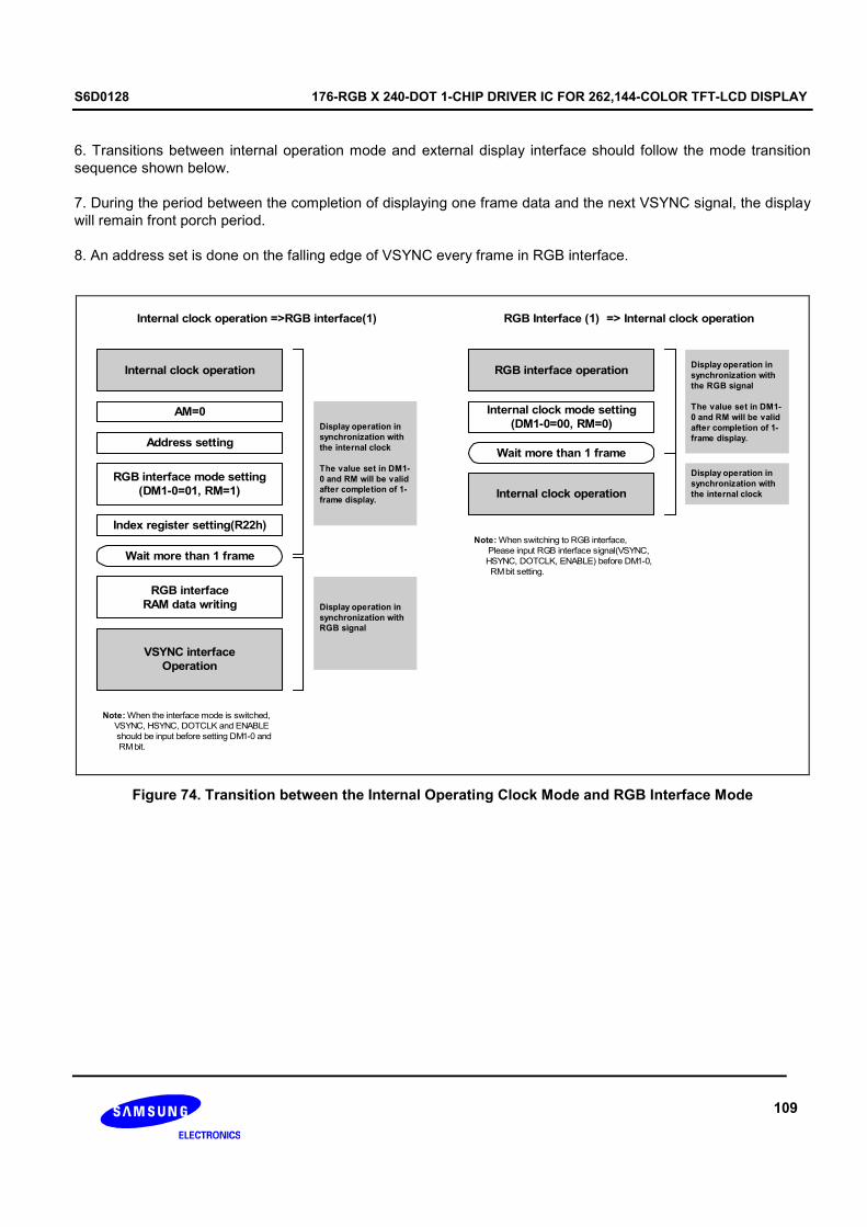
S6D0128 176-RGB X 240-DOT 1-CHIP DRIVER IC FOR 262,144-COLOR TFT-LCD DISPLAY
109
6. Transitions between internal operation mode and external display interface should follow the mode transition
sequence shown below.
7. During the period between the completion of displaying one frame data and the next VSYNC signal, the display
will remain front porch period.
8. An address set is done on the falling edge of VSYNC every frame in RGB interface.
AM=0
Address setting
RGB interface mode setting
(DM1-0=01, RM=1)
Index register setting(R22h)
Wait more than 1 frame
RGB interface
RAM data writing
VSYNC interface
Operation
Internal clock operation
Display operation in
synchronization with
the internal clock
The value set in DM1-
0 and RM will be valid
after completion of 1-
frame display.
Display operation in
synchronization with
RGB signal
Note: When the interface mode is switched,
VSYNC, HSYNC, DOTCLK and ENABLE
should be input before setting DM1-0 and
RM bit.
Internal clock operation =>RGB interface(1)
Wait more than 1 frame
Internal clock mode setting
(DM1-0=00, RM=0)
Internal clock operation
RGB interface operationDisplay operation in
synchronization with
the RGB signal
The value set in DM1-
0 and RM will be valid
after completion of 1-
frame display.
Display operation in
synchronization with
the internal clock
Note: When switching to RGB interface,
Please input RGB interface signal(VSYNC,
HSYNC, DOTCLK, ENABLE) before DM1-0,
RM bit setting.
RGB Interface (1) => Internal clock operation
Figure 74. Transition between the Internal Operating Clock Mode and RGB Interface Mode

176-RGB X 240-DOT 1-CHIP DRIVER IC FOR 262,144-COLOR TFT-LCD DISPLAY S6D0128
110
WINDOW ADDRESS FUNCTION
When data is written to the on-chip GRAM, a window address-range that is specified by the horizontal address
register (start: HSA7-0, end: HEA 7-0) and vertical address register (start: VSA7-0, end: VEA7-0) can be updated
consecutively.
Data is written to addresses in the direction specified by the I/D1-0bit. When image data, etc. is being written, data
can be written consecutively without thinking a data wrap by doing this.
The window must be specified to be within the GRAM address area described as following example. Addresses
must be set within the window address.
[Restriction on window address-
(horizontal direction) 00H≤HSA7-0 ≤HEA7-0 ≤ AFH
(vertical direction) 00H ≤VSA7-0 ≤VEA7-0 ≤ H
[Restriction on address settings during the window address](RAM address) HSA7-0≤AD7-0 ≤HEA7-0
VSA7-0 ≤AD15-8 ≤VEA7-0
[Restriction on window address range settings]
(horizontal direction) 00H≤HSA7-0 ≤HEA7-0 ≤ H
(vertical direction) 00H ≤VSA7-0 ≤VEA7-0 ≤ H
[Restriction on address settings during the window address](RAM address) HSA7 ≤AD7-0 ≤HEA7-0
VSA7-0 ≤AD15-8 ≤VEA7-0
EF
“2010”H “202F”H“2110”H
“5F10”H “EFAF”H
“212F”H
GRAM address map
Window address-range specification areaHSA7-0 = HSE7-0 = I/D = 1 (increment)VSA7-0 = VEA7-0 =
Window address-range specification areaHSA7-0 = -0 = I/D = 1 (increment)VSA7-0 = -0 =
“10”H“20”H
“2F”H“5F”H
“0000”H “00AF”H
“EFAF”H“EF00”H
Figure 75. Example of address operation in the window address specification

S6D0128 176-RGB X 240-DOT 1-CHIP DRIVER IC FOR 262,144-COLOR TFT-LCD DISPLAY
111
GATE DRIVER SCAN MODE SETTING
SM and GS bit set the gate scan mode of S6D0128. GS bit determines the scan direction whether the gate driver
scans forward or reverse direction. SM bit determines the method of display division (Even/Odd or Upper/Lower
division drive). Using this function, various connections between S6D0128 and the liquid crystal panels can be
accomplished.
Figure 76. Scan mode setting
SM GS Scan Mode
0 0
G1
G239
G2
G240
ODD EVENTFT
Panel
G1 G239 G240 G2
S6D0128
G1G2G3
G4····G237
G238G239G240
0 1
S6D0128
G1 G239 G240 G2
G1
G239
G2
G240
ODD EVENTFT
Panel
G240G239G238
G237····G4
G3G2G1
1 0
G1
G239
G2
G240
TFT
Panel
G1 G239 G240 G2
S6D0128
G1G3
G5····G237G239
G2G4
G6····G238G240
1 1
G1
G239
G2
G240
TFT
Panel
G1 G239 G240 G2
S6D0128
G240G238
G172····G4G2
G239G237
G171····G3G1

176-RGB X 240-DOT 1-CHIP DRIVER IC FOR 262,144-COLOR TFT-LCD DISPLAY S6D0128
112
GAMMA ADJUSTMENT FUNCTION
The S6D0128 provides the gamma adjustment function to display 262,144 colors simultaneously. The gamma
adjustment executed by the gradient adjustment register and the micro-adjustment register that determines 8
grayscale levels. Furthermore, since the gradient adjustment register and the micro-adjustment register have the
positive polarities and negative polarities, adjust them to match LCD panel respectively.
64 grayscale
control
<R>
64 grayscale
control
<G>
64 grayscale
control
<B>
LCD driver LCD driver LCD driver
R G B
LCD
6 6 6V0
V1
V63
Grayscale
Amplifier
64
PKN00PKN01PKN02
PKN10PKN11PKN12
PKN20PKN21PKN22
PKN30PKN31PKN32
PKN40PKN41PKN42
PKN50PKN51PKN52
PRN00PRN01PRN02
PRN10PRN11PRN12
VRN00VRN01VRN02
VRN10VRN11VRN12
VRN03
VRN13VRN14
Negative
polarity
register
PKP00PKP01PKP02
PKP10PKP11PKP12
PKP20PKP21PKP22
PKP30PKP31PKP32
PKP40PKP41PKP42
PKP50PKP51PKP52
PRP00PRP01PRP02
PRP10PRP11PRP12
VRP00VRP01VRP02
VRP10VRP11VRP12
VRP03
VRP13VRP14
Positive
polarity
register
GRAM
R5 R4 R3 R2 R1 R0 G5 G4 G3 G2 G1 G0 B5 B4 B3 B2 B1 B0
MSB ----------------------------------------------------------------------------------------------------------------------------------------------LSB
8
Figure 77. Grayscale control
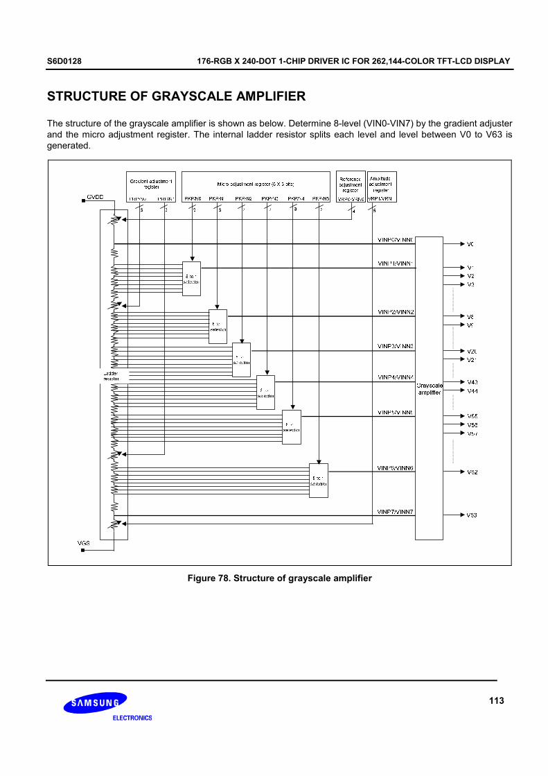
S6D0128 176-RGB X 240-DOT 1-CHIP DRIVER IC FOR 262,144-COLOR TFT-LCD DISPLAY
113
STRUCTURE OF GRAYSCALE AMPLIFIER
The structure of the grayscale amplifier is shown as below. Determine 8-level (VIN0-VIN7) by the gradient adjuster
and the micro adjustment register. The internal ladder resistor splits each level and level between V0 to V63 is
generated.
Figure 78. Structure of grayscale amplifier

176-RGB X 240-DOT 1-CHIP DRIVER IC FOR 262,144-COLOR TFT-LCD DISPLAY S6D0128
114
Figure 79. Structure of Ladder / 8 to 1 selector

S6D0128 176-RGB X 240-DOT 1-CHIP DRIVER IC FOR 262,144-COLOR TFT-LCD DISPLAY
115
GAMMA ADJUSTMENT REGISTER
This block has the register to set up the grayscale voltage adjusting to the gamma specification of the LCD panel.
These registers can independently set up to positive/negative polarities and there are 4 types of register groups to
adjust gradient and amplitude on number of the grayscale, characteristics of the grayscale voltage. (average
<R><G><B> are common.) The following figure indicates the operation of each adjusting register.
Grayscale Number
Grayscale Voltage
a) Gradient adjustment
Grayscale Number
Grayscale Voltage
b) Amplitude adjustment
Grayscale Number
Grayscale Voltage
d) Micro-adjustment
Grayscale NumberGrayscale Voltage
c) Reference adjustment
Figure 80. The operation of adjusting register
a) Gradient adjustment resistor
The gradient adjustment resistors are used to adjust the gradient in the middle of the grayscale characteristics for
the voltage without changing the dynamic range. To accomplish the adjustment, it controls the variable resistor
(VRHP(N) / VRLP(N)) of the ladder resistor for the grayscale voltage generator. Also, there is an independent
resistor on the positive/negative polarities in order for corresponding to asymmetry drive.
b) Amplitude adjustment resistor
The amplitude-adjusting resistor is to adjust amplitude of the grayscale voltage. To accomplish the adjustment, it
controls the variable resistor (VRP(N)1) of the ladder resistor for the grayscale voltage generator located at lower
side of the ladder resistor. (Adjust upper side by input GVDD level.) Also, there is an independent resistor on the
positive/negative polarities as well as the gradient-adjusting resistor.
c) Reference adjustment resistor
The Reference-adjusting resistor is to adjust reference of the grayscale voltage. To accomplish the adjustment, it
controls the variable resistor (VRP(N)0) of the ladder resistor for the grayscale voltage generator located at upper
side of the ladder resistor.
d) Micro adjustment resistor
The micro adjustment resistor is to make subtle adjustment of the grayscale voltage level. To accomplish the
adjustment, it controls the each reference voltage level by the 8 to 1 selector towards the 8-leveled reference voltage
generated from the ladder resistor. Also, there is an independent resistor on the positive/negative polarities as well
as other adjusting resistors.

176-RGB X 240-DOT 1-CHIP DRIVER IC FOR 262,144-COLOR TFT-LCD DISPLAY S6D0128
116
Table 37. Gamma correction registers
Register Positive polarity Negative polarity Set-up contents
PRP0[2:0] PRN0[2:0] Variable resistor VRHP(N) Gradient adjustment
PRP1[2:0] PRN1[2:0] Variable resistor VRLP(N)
Amplitude adjustment VRP1[4:0] VRN1[4:0] Variable resistor VRP(N)1
Reference adjustment VRP0[3:0] VRN0[3:0] Variable resistor VRP(N)0
PKP0[2:0] PKN0[2:0] The voltage of grayscale number 1 is
selected by the 8 to 1 selector
PKP1[2:0] PKN1[2:0] The voltage of grayscale number 8 is
selected by the 8 to 1 selector
PKP2[2:0] PKN2[2:0] The voltage of grayscale number 20 is
selected by the 8 to 1 selector
PKP3[2:0] PKN3[2:0] The voltage of grayscale number 43 is
selected by the 8 to 1 selector
PKP4[2:0] PKN4[2:0] The voltage of grayscale number 55 is
selected by the 8 to 1 selector
Micro-adjustment
PKP5[2:0] PKN5[2:0] The voltage of grayscale number 62 is
selected by the 8 to 1 selector

S6D0128 176-RGB X 240-DOT 1-CHIP DRIVER IC FOR 262,144-COLOR TFT-LCD DISPLAY
117
LADDER RESISTOR/8 TO 1 SELECTOR
This block outputs the reference voltage of the grayscale voltage. There are two ladder resistors including the
variable resistor and the 8 to 1 selector selecting voltage generated by the ladder resistance voltage. The variable
and 8 to 1 resistors are controlled by the gamma resistor. Also, there are pins that connect to the external volume
resistor. In addition, it allows compensating the dispersion of length between one panel to another.
VARIABLE RESISTOR
There are 3 types of the variable resistors that is for the gradient adjustment (VRHP(N) / VRLP(N)), for the
reference adjustment (VRP(N)0) and for the amplitude adjustment (VRP(N)1). The resistance value is set by the
gradient adjusting resistor and the amplitude adjustment resistor as below.
Table 38. Gradient Adjustment (1)
Register value PRP(N)0 [2:0] Resistance value VRHP(N)
000 0R
001 4R
010 8R
011 12R
100 16R
101 20R
110 24R
111 28R
Table 39. Gradient Adjustment (2)
Register value PRP(N)1 [2:0] Resistance value VRLP(N)
000 0R
001 4R
010 8R
011 12R
100 16R
101 20R
110 24R
111 28R
Table 40. Reference Adjustment
Register value VRP(N)0 [3:0] Resistance value VRP(N)0
0000 0R
0001 2R
0010 4R
.
.
.
.
.
.
1101 26R
1110 28R
1111 30R
Table 41. Amplitude Adjustment

176-RGB X 240-DOT 1-CHIP DRIVER IC FOR 262,144-COLOR TFT-LCD DISPLAY S6D0128
118
Register value VRP(N)1[4:0] Resistance value VRP(N)1
00000 0R
00001 1R
00010 2R
.
.
.
.
.
.
11101 29R
11110 30R
11111 31R
THE 8 TO 1 SELECTOR
In the 8 to 1 selector, the voltage level must be selected given by the ladder resistance and the micro-adjusting
register. And output the voltage the six types of the reference voltage, the VIN1- to VIN6.
Following table explains the relationship between the micro-adjusting register and the selecting voltage.
Table 42. Relationship between Micro-adjustment Register and Selected Voltage
Selected voltage Register value
PKP(N) [2:0] VINP(N)1 VINP(N)2 VINP(N)3 VINP(N)4 VINP(N)5 VINP(N)6
000 KVP(N)1 KVP(N)9 KVP(N)17 KVP(N)25 KVP(N)33 KVP(N)41
001 KVP(N)2 KVP(N)10 KVP(N)18 KVP(N)26 KVP(N)34 KVP(N)42
010 KVP(N)3 KVP(N)11 KVP(N)19 KVP(N)27 KVP(N)35 KVP(N)43
011 KVP(N)4 KVP(N)12 KVP(N)20 KVP(N)28 KVP(N)36 KVP(N)44
100 KVP(N)5 KVP(N)13 KVP(N)21 KVP(N)29 KVP(N)37 KVP(N)45
101 KVP(N)6 KVP(N)14 KVP(N)22 KVP(N)30 KVP(N)38 KVP(N)46
110 KVP(N)7 KVP(N)15 KVP(N)23 KVP(N)31 KVP(N)39 KVP(N)47
111 KVP(N)8 KVP(N)16 KVP(N)24 KVP(N)32 KVP(N)40 KVP(N)48
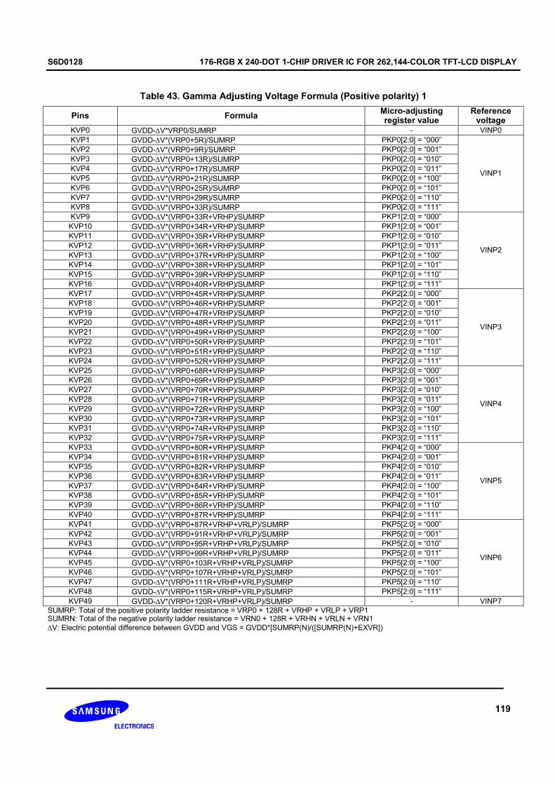
S6D0128 176-RGB X 240-DOT 1-CHIP DRIVER IC FOR 262,144-COLOR TFT-LCD DISPLAY
119
Table 43. Gamma Adjusting Voltage Formula (Positive polarity) 1
Pins Formula Micro-adjusting register value
Reference voltage
KVP0 GVDD-∆V*VRP0/SUMRP - VINP0
KVP1 GVDD-∆V*(VRP0+5R)/SUMRP PKP0[2:0] = “000”
KVP2 GVDD-∆V*(VRP0+9R)/SUMRP PKP0[2:0] = “001”
KVP3 GVDD-∆V*(VRP0+13R)/SUMRP PKP0[2:0] = “010”
KVP4 GVDD-∆V*(VRP0+17R)/SUMRP PKP0[2:0] = “011”
KVP5 GVDD-∆V*(VRP0+21R)/SUMRP PKP0[2:0] = “100”
KVP6 GVDD-∆V*(VRP0+25R)/SUMRP PKP0[2:0] = “101”
KVP7 GVDD-∆V*(VRP0+29R)/SUMRP PKP0[2:0] = “110”
KVP8 GVDD-∆V*(VRP0+33R)/SUMRP PKP0[2:0] = “111”
VINP1
KVP9 GVDD-∆V*(VRP0+33R+VRHP)/SUMRP PKP1[2:0] = “000”
KVP10 GVDD-∆V*(VRP0+34R+VRHP)/SUMRP PKP1[2:0] = “001”
KVP11 GVDD-∆V*(VRP0+35R+VRHP)/SUMRP PKP1[2:0] = “010”
KVP12 GVDD-∆V*(VRP0+36R+VRHP)/SUMRP PKP1[2:0] = “011”
KVP13 GVDD-∆V*(VRP0+37R+VRHP)/SUMRP PKP1[2:0] = “100”
KVP14 GVDD-∆V*(VRP0+38R+VRHP)/SUMRP PKP1[2:0] = “101”
KVP15 GVDD-∆V*(VRP0+39R+VRHP)/SUMRP PKP1[2:0] = “110”
KVP16 GVDD-∆V*(VRP0+40R+VRHP)/SUMRP PKP1[2:0] = “111”
VINP2
KVP17 GVDD-∆V*(VRP0+45R+VRHP)/SUMRP PKP2[2:0] = “000”
KVP18 GVDD-∆V*(VRP0+46R+VRHP)/SUMRP PKP2[2:0] = “001”
KVP19 GVDD-∆V*(VRP0+47R+VRHP)/SUMRP PKP2[2:0] = “010”
KVP20 GVDD-∆V*(VRP0+48R+VRHP)/SUMRP PKP2[2:0] = “011”
KVP21 GVDD-∆V*(VRP0+49R+VRHP)/SUMRP PKP2[2:0] = “100”
KVP22 GVDD-∆V*(VRP0+50R+VRHP)/SUMRP PKP2[2:0] = “101”
KVP23 GVDD-∆V*(VRP0+51R+VRHP)/SUMRP PKP2[2:0] = “110”
KVP24 GVDD-∆V*(VRP0+52R+VRHP)/SUMRP PKP2[2:0] = “111”
VINP3
KVP25 GVDD-∆V*(VRP0+68R+VRHP)/SUMRP PKP3[2:0] = “000”
KVP26 GVDD-∆V*(VRP0+69R+VRHP)/SUMRP PKP3[2:0] = “001”
KVP27 GVDD-∆V*(VRP0+70R+VRHP)/SUMRP PKP3[2:0] = “010”
KVP28 GVDD-∆V*(VRP0+71R+VRHP)/SUMRP PKP3[2:0] = “011”
KVP29 GVDD-∆V*(VRP0+72R+VRHP)/SUMRP PKP3[2:0] = “100”
KVP30 GVDD-∆V*(VRP0+73R+VRHP)/SUMRP PKP3[2:0] = “101”
KVP31 GVDD-∆V*(VRP0+74R+VRHP)/SUMRP PKP3[2:0] = “110”
KVP32 GVDD-∆V*(VRP0+75R+VRHP)/SUMRP PKP3[2:0] = “111”
VINP4
KVP33 GVDD-∆V*(VRP0+80R+VRHP)/SUMRP PKP4[2:0] = “000”
KVP34 GVDD-∆V*(VRP0+81R+VRHP)/SUMRP PKP4[2:0] = “001”
KVP35 GVDD-∆V*(VRP0+82R+VRHP)/SUMRP PKP4[2:0] = “010”
KVP36 GVDD-∆V*(VRP0+83R+VRHP)/SUMRP PKP4[2:0] = “011”
KVP37 GVDD-∆V*(VRP0+84R+VRHP)/SUMRP PKP4[2:0] = “100”
KVP38 GVDD-∆V*(VRP0+85R+VRHP)/SUMRP PKP4[2:0] = “101”
KVP39 GVDD-∆V*(VRP0+86R+VRHP)/SUMRP PKP4[2:0] = “110”
KVP40 GVDD-∆V*(VRP0+87R+VRHP)/SUMRP PKP4[2:0] = “111”
VINP5
KVP41 GVDD-∆V*(VRP0+87R+VRHP+VRLP)/SUMRP PKP5[2:0] = “000”
KVP42 GVDD-∆V*(VRP0+91R+VRHP+VRLP)/SUMRP PKP5[2:0] = “001”
KVP43 GVDD-∆V*(VRP0+95R+VRHP+VRLP)/SUMRP PKP5[2:0] = “010”
KVP44 GVDD-∆V*(VRP0+99R+VRHP+VRLP)/SUMRP PKP5[2:0] = “011”
KVP45 GVDD-∆V*(VRP0+103R+VRHP+VRLP)/SUMRP PKP5[2:0] = “100”
KVP46 GVDD-∆V*(VRP0+107R+VRHP+VRLP)/SUMRP PKP5[2:0] = “101”
KVP47 GVDD-∆V*(VRP0+111R+VRHP+VRLP)/SUMRP PKP5[2:0] = “110”
KVP48 GVDD-∆V*(VRP0+115R+VRHP+VRLP)/SUMRP PKP5[2:0] = “111”
VINP6
KVP49 GVDD-∆V*(VRP0+120R+VRHP+VRLP)/SUMRP - VINP7
SUMRP: Total of the positive polarity ladder resistance = VRP0 + 128R + VRHP + VRLP + VRP1 SUMRN: Total of the negative polarity ladder resistance = VRN0 + 128R + VRHN + VRLN + VRN1
∆V: Electric potential difference between GVDD and VGS = GVDD*[SUMRP(N)/([SUMRP(N)+EXVR])

176-RGB X 240-DOT 1-CHIP DRIVER IC FOR 262,144-COLOR TFT-LCD DISPLAY S6D0128
120
Table 44. Gamma Voltage Formula (Positive Polarity) 2
Grayscale voltage Formula Grayscale voltage Formula
V0 VINP0 V32 V43+(V20-V43)*(11/23) V1 VINP1 V33 V43+(V20-V43)*(10/23) V2 V3+(V1-V3)*(8/24) V34 V43+(V20-V43)*(9/23)
V3 V8+(V1-V8)*(450/800) V35 V43+(V20-V43)*(8/23) V4 V8+(V3-V8)*(16/24) V36 V43+(V20-V43)*(7/23) V5 V8+(V3-V8)*(12/24) V37 V43+(V20-V43)*(6/23) V6 V8+(V3-V8)*(8/24) V38 V43+(V20-V43)*(5/23)
V7 V8+(V3-V8)*(4/24) V39 V43+(V20-V43)*(4/23) V8 VINP2 V40 V43+(V20-V43)*(3/23) V9 V20+(V8-V20)*(22/24) V41 V43+(V20-V43)*(2/23) V10 V20+(V8-V20)*(20/24) V42 V43+(V20-V43)*(1/23)
V11 V20+(V8-V20)*(18/24) V43 VINP4 V12 V20+(V8-V20)*(16/24) V44 V55+(V43-V55)*(22/24) V13 V20+(V8-V20)*(14/24) V45 V55+(V43-V55)*(20/24) V14 V20+(V8-V20)*(12/24) V46 V55+(V43-V55)*(18/24)
V15 V20+(V8-V20)*(10/24) V47 V55+(V43-V55)*(16/24) V16 V20+(V8-V20)*(8/24) V48 V55+(V43-V55)*(14/24) V17 V20+(V8-V20)*(6/24) V49 V55+(V43-V55)*(12/24) V18 V20+(V8-V20)*(4/24) V50 V55+(V43-V55)*(10/24)
V19 V20+(V8-V20)*(2/24) V51 V55+(V43-V55)*(8/24) V20 VINP3 V52 V55+(V43-V55)*(6/24) V21 V43+(V20-V43)*(22/23) V53 V55+(V43-V55)*(4/24) V22 V43+(V20-V43)*(21/23) V54 V55+(V43-V55)*(2/24)
V23 V43+(V20-V43)*(20/23) V55 VINP5 V24 V43+(V20-V43)*(19/23) V56 V60+(V55-V60)*(20/24) V25 V43+(V20-V43)*(18/23) V57 V60+(V55-V60)*(16/24) V26 V43+(V20-V43)*(17/23) V58 V60+(V55-V60)*(12/24)
V27 V43+(V20-V43)*(16/23) V59 V60+(V55-V60)*(8/24) V28 V43+(V20-V43)*(15/23) V60 V62+(V55-V62)*(350/800) V29 V43+(V20-V43)*(14/23) V61 V62+(V60-V62)*(16/24) V30 V43+(V20-V43)*(13/23) V62 VINP6
V31 V43+(V20-V43)*(12/23) V63 VINP7

S6D0128 176-RGB X 240-DOT 1-CHIP DRIVER IC FOR 262,144-COLOR TFT-LCD DISPLAY
121
Table 45. Gamma Adjusting Voltage Formula (Negative polarity) 1
Pins Formula Micro-adjusting register value
Reference voltage
KVN0 GVDD-∆V*VRN0/SUMRN - VINN0 KVN1 GVDD-∆V*(VRN0+5R)/SUMRN PKN0[2:0] = “000”
KVN2 GVDD-∆V*(VRN0+9R)/SUMRN PKN0[2:0] = “001”
KVN3 GVDD-∆V*(VRN0+13R)/SUMRN PKN0[2:0] = “010”
KVN4 GVDD-∆V*(VRN0+17R)/SUMRN PKN0[2:0] = “011”
KVN5 GVDD-∆V*(VRN0+21R)/SUMRN PKN0[2:0] = “100”
KVN6 GVDD-∆V*(VRN0+25R)/SUMRN PKN0[2:0] = “101”
KVN7 GVDD-∆V*(VRN0+29R)/SUMRN PKN0[2:0] = “110”
KVN8 GVDD-∆V*(VRN0+33R)/SUMRN PKN0[2:0] = “111”
VINN1
KVN9 GVDD-∆V*(VRN0+33R+VRHN)/SUMRN PKN1[2:0] = “000”
KVN10 GVDD-∆V*(VRN0+34R+VRHN)/SUMRN PKN1[2:0] = “001”
KVN11 GVDD-∆V*(VRN0+35R+VRHN)/SUMRN PKN1[2:0] = “010”
KVN12 GVDD-∆V*(VRN0+36R+VRHN)/SUMRN PKN1[2:0] = “011”
KVN13 GVDD-∆V*(VRN0+37R+VRHN)/SUMRN PKN1[2:0] = “100”
KVN14 GVDD-∆V*(VRN0+38R+VRHN)/SUMRN PKN1[2:0] = “101”
KVN15 GVDD-∆V*(VRN0+39R+VRHN)/SUMRN PKN1[2:0] = “110”
KVN16 GVDD-∆V*(VRN0+40R+VRHN)/SUMRN PKN1[2:0] = “111”
VINN2
KVN17 GVDD-∆V*(VRN0+45R+VRHN)/SUMRN PKN2[2:0] = “000”
KVN18 GVDD-∆V*(VRN0+46R+VRHN)/SUMRN PKN2[2:0] = “001”
KVN19 GVDD-∆V*(VRN0+47R+VRHN)/SUMRN PKN2[2:0] = “010”
KVN20 GVDD-∆V*(VRN0+48R+VRHN)/SUMRN PKN2[2:0] = “011”
KVN21 GVDD-∆V*(VRN0+49R+VRHN)/SUMRN PKN2[2:0] = “100”
KVN22 GVDD-∆V*(VRN0+50R+VRHN)/SUMRN PKN2[2:0] = “101”
KVN23 GVDD-∆V*(VRN0+51R+VRHN)/SUMRN PKN2[2:0] = “110”
KVN24 GVDD-∆V*(VRN0+52R+VRHN)/SUMRN PKN2[2:0] = “111”
VINN3
KVN25 GVDD-∆V*(VRN0+68R+VRHN)/SUMRN PKN3[2:0] = “000”
KVN26 GVDD-∆V*(VRN0+69R+VRHN)/SUMRN PKN3[2:0] = “001”
KVN27 GVDD-∆V*(VRN0+70R+VRHN)/SUMRN PKN3[2:0] = “010”
KVN28 GVDD-∆V*(VRN0+71R+VRHN)/SUMRN PKN3[2:0] = “011”
KVN29 GVDD-∆V*(VRN0+72R+VRHN)/SUMRN PKN3[2:0] = “100”
KVN30 GVDD-∆V*(VRN0+73R+VRHN)/SUMRN PKN3[2:0] = “101”
KVN31 GVDD-∆V*(VRN0+74R+VRHN)/SUMRN PKN3[2:0] = “110”
KVN32 GVDD-∆V*(VRN0+75R+VRHN)/SUMRN PKN3[2:0] = “111”
VINN4
KVN33 GVDD-∆V*(VRN0+80R+VRHN)/SUMRN PKN4[2:0] = “000”
KVN34 GVDD-∆V*(VRN0+81R+VRHN)/SUMRN PKN4[2:0] = “001”
KVN35 GVDD-∆V*(RN0+82R+VRHN)/SUMRN PKN4[2:0] = “010”
KVN36 GVDD-∆V*(VRN0+83R+VRHN)/SUMRN PKN4[2:0] = “011”
KVN37 GVDD-∆V*(VRN0+84R+VRHN)/SUMRN PKN4[2:0] = “100”
KVN38 GVDD-∆V*(VRN0+85R+VRHN)/SUMRN PKN4[2:0] = “101”
KVN39 GVDD-∆V*(VRN0+86R+VRHN)/SUMRN PKN4[2:0] = “110”
KVN40 GVDD-∆V*(VRN0+87R+VRHN)/SUMRN PKN4[2:0] = “111”
VINN5
KVN41 GVDD-∆V*(VRN0+87R+VRHN+VRLN)/SUMRN PKN5[2:0] = “000”
KVN42 GVDD-∆V*(VRN0+91R+VRHN+VRLN)/SUMRN PKN5[2:0] = “001”
KVN43 GVDD-∆V*(VRN0+95R+VRHN+VRLN)/SUMRN PKN5[2:0] = “010”
KVN44 GVDD-∆V*(VRN0+99R+VRHN+VRLN)/SUMRN PKN5[2:0] = “011”
KVN45 GVDD-∆V*(VRN0+103R+VRHN+VRLN)/SUMRN PKN5[2:0] = “100”
KVN46 GVDD-∆V*(VRN0+107R+VRHN+VRLN)/SUMRN PKN5[2:0] = “101”
KVN47 GVDD-∆V*(VRN0+111R+VRHN+VRLN)/SUMRN PKN5[2:0] = “110”
KVN48 GVDD-∆V*(VRN0+115R+VRHN+VRLN)/SUMRN PKN5[2:0] = “111”
VINN6
KVN49 GVDD-∆V*(VRN0+120R+VRHN+VRLN)/SUMRN - VINN7
SUMRP: Total of the positive polarity ladder resistance = VRP0 + 128R + VRHP + VRLP + VRP1 SUMRN: Total of the negative polarity ladder resistance = VRN0 + 128R + VRHN + VRLN + VRN1
∆V: Electric potential difference between GVDD and VGS = GVDD*[SUMRP(N)/([SUMRP(N)+EXVR]

176-RGB X 240-DOT 1-CHIP DRIVER IC FOR 262,144-COLOR TFT-LCD DISPLAY S6D0128
122
Table 46. Gamma Voltage Formula (Negative Polarity) 2
Grayscale voltage Formula Grayscale voltage Formula
V0 VINN0 V32 V43+(V20-V43)*(11/23) V1 VINN1 V33 V43+(V20-V43)*(10/23) V2 V3+(V1-V3)*(8/24) V34 V43+(V20-V43)*(9/23)
V3 V8+(V1-V8)*(450/800) V35 V43+(V20-V43)*(8/23) V4 V8+(V3-V8)*(16/24) V36 V43+(V20-V43)*(7/23) V5 V8+(V3-V8)*(12/24) V37 V43+(V20-V43)*(6/23) V6 V8+(V3-V8)*(8/24) V38 V43+(V20-V43)*(5/23)
V7 V8+(V3-V8)*(4/24) V39 V43+(V20-V43)*(4/23) V8 VINN2 V40 V43+(V20-V43)*(3/23) V9 V20+(V8-V20)*(22/24) V41 V43+(V20-V43)*(2/23) V10 V20+(V8-V20)*(20/24) V42 V43+(V20-V43)*(1/23)
V11 V20+(V8-V20)*(18/24) V43 VINN4 V12 V20+(V8-V20)*(16/24) V44 V55+(V43-V55)*(22/24) V13 V20+(V8-V20)*(14/24) V45 V55+(V43-V55)*(20/24) V14 V20+(V8-V20)*(12/24) V46 V55+(V43-V55)*(18/24)
V15 V20+(V8-V20)*(10/24) V47 V55+(V43-V55)*(16/24) V16 V20+(V8-V20)*(8/24) V48 V55+(V43-V55)*(14/24) V17 V20+(V8-V20)*(6/24) V49 V55+(V43-V55)*(12/24) V18 V20+(V8-V20)*(4/24) V50 V55+(V43-V55)*(10/24)
V19 V20+(V8-V20)*(2/24) V51 V55+(V43-V55)*(8/24) V20 VINN3 V52 V55+(V43-V55)*(6/24) V21 V43+(V20-V43)*(22/23) V53 V55+(V43-V55)*(4/24) V22 V43+(V20-V43)*(21/23) V54 V55+(V43-V55)*(2/24)
V23 V43+(V20-V43)*(20/23) V55 VINN5 V24 V43+(V20-V43)*(19/23) V56 V60+(V55-V60)*(20/24) V25 V43+(V20-V43)*(18/23) V57 V60+(V55-V60)*(16/24) V26 V43+(V20-V43)*(17/23) V58 V60+(V55-V60)*(12/24)
V27 V43+(V20-V43)*(16/23) V59 V60+(V55-V60)*(8/24) V28 V43+(V20-V43)*(15/23) V60 V62+(V55-V62)*(350/800) V29 V43+(V20-V43)*(14/23) V61 V62+(V60-V62)*(16/24) V30 V43+(V20-V43)*(13/23) V62 VINN6
V31 V43+(V20-V43)*(12/23) V63 VINN7
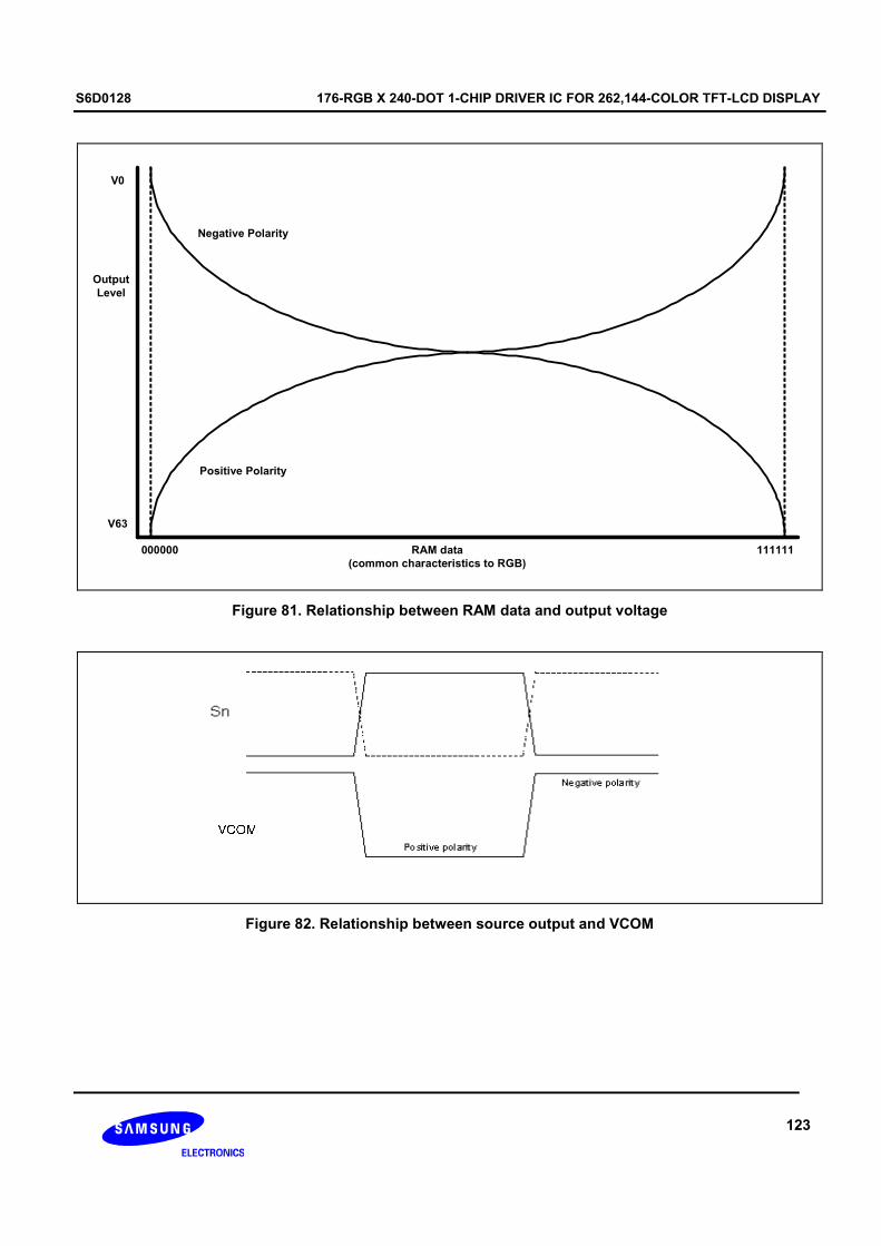
S6D0128 176-RGB X 240-DOT 1-CHIP DRIVER IC FOR 262,144-COLOR TFT-LCD DISPLAY
123
000000 111111
V63
V0
Output
Level
Negative Polarity
Positive Polarity
RAM data
(common characteristics to RGB)
Figure 81. Relationship between RAM data and output voltage
Figure 82. Relationship between source output and VCOM

176-RGB X 240-DOT 1-CHIP DRIVER IC FOR 262,144-COLOR TFT-LCD DISPLAY S6D0128
124
THE 8-COLOR DISPLAY MODE
The S6D0128 incorporates 8-color display mode. The grayscale levels (V0~V63) are all halt. So that it attempts to
lower power consumption.
During the 8-color mode, the Gamma micro adjustment register, Gradient adjustment register, Amplitude
adjustment register and Reference adjustment register are invalid.
The level power supply (V0-V63) is in OFF condition during the 8-color mode in order to select AVSS/GVDD.
GRAM
R5 R4 R3 R2 R1 R0 G5 G4 G3 G2 G1 G0 B5 B4 B3 B2 B1 B0
MSB ----------------------------------------------------------------------------------------------------------------------------------------------LSB
BINARY
DRIVER
BINARY
DRIVER
BINARY
DRIVER
R G B
LCD
1
MSB
GVDD
AVSS
1
MSB
1
MSB
Figure 83. 8-color display control

S6D0128 176-RGB X 240-DOT 1-CHIP DRIVER IC FOR 262,144-COLOR TFT-LCD DISPLAY
125
OFF
GON = “1”
D1-0 = “10”
OFF
GON = “0”
D1-0 = “00”
Wait (2 frame or higher)
RAM setup
CL = “1”
Wait (40ms or higher)
OFF
GON = “1”
D1-0 = “01”
ON
GON = “1”
D1-0 = “11”
Display by 8 -color mode
OFF
GON = “1”
D1-0 = “10”
OFF
GON = “0”
D1-0 = “00”
Wait (2 frame or higher)
RAM setup
CL = “0”
Wait (40ms or higher)
OFF
GON = “1”
D1-0 = “01”
ON
GON = “1”
D1-0 = “11”
Display
by 262,144 -color mode
Wait (2 frame or higher) Wait (2 frame or higher)
262,144 -color => 8 -color 8-color => 262,144 -color
Figure 84. Set up procedure for the 8-color mode

176-RGB X 240-DOT 1-CHIP DRIVER IC FOR 262,144-COLOR TFT-LCD DISPLAY S6D0128
126
SYSTEM STRUCTURE EXAMPLE
The following figure indicates the system structure, which composes the 176 (width) x 240 (length) dots TFT-LCD
panel.
Figure 85. System structure

S6D0128 176-RGB X 240-DOT 1-CHIP DRIVER IC FOR 262,144-COLOR TFT-LCD DISPLAY
127
OSCILLATOR CIRCUIT
The S6D0128 can oscillate between the OSC1 and OSC2 pins using an internal R-C oscillator with an external
oscillator resistor. Note that in R-C oscillation, the oscillator frequency is changed according to the external resistor
value, wiring length, or operating power-supply voltage. If Rf is increased or power supply voltage is decrease, the
oscillation frequency decreases. For the relationship between Rf resistor value and oscillation frequency, see the
Electric Characteristics Notes section.
Figure 86. Oscillation Circuit
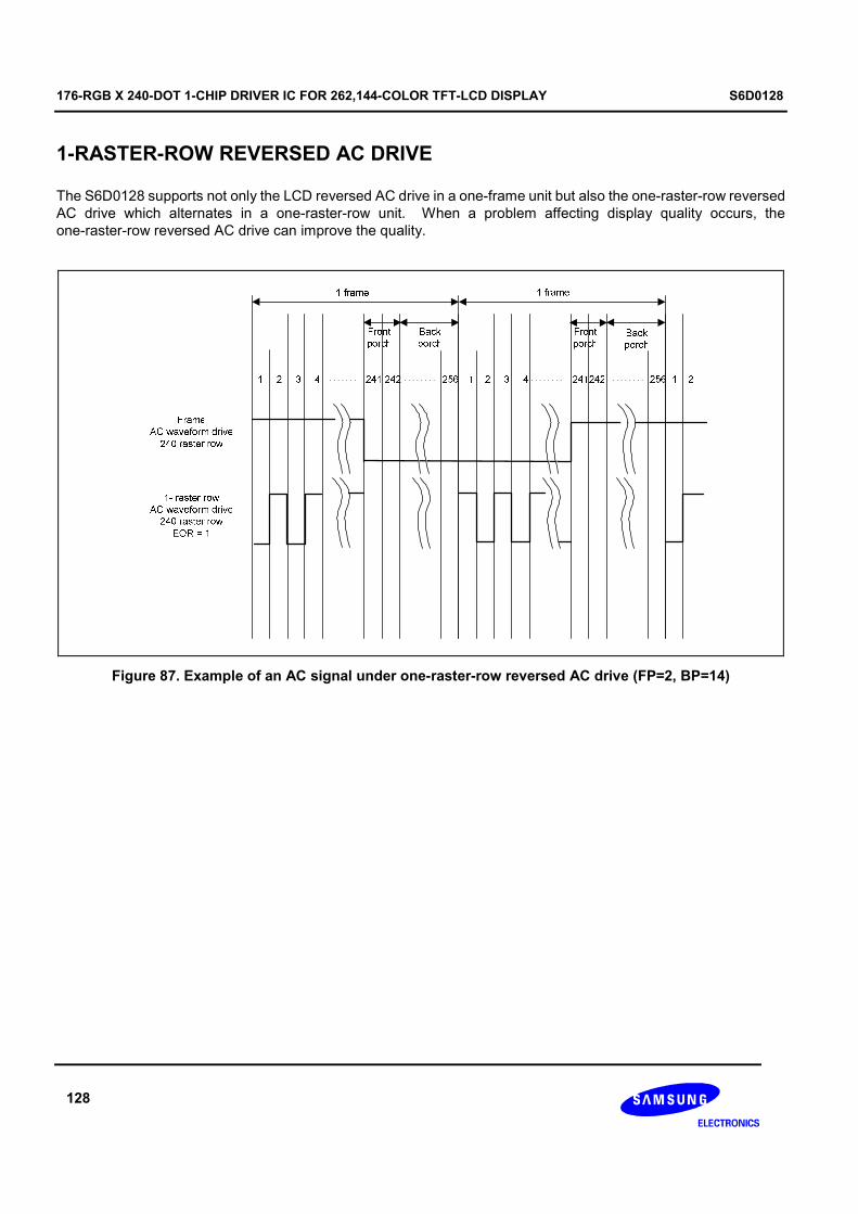
176-RGB X 240-DOT 1-CHIP DRIVER IC FOR 262,144-COLOR TFT-LCD DISPLAY S6D0128
128
1-RASTER-ROW REVERSED AC DRIVE
The S6D0128 supports not only the LCD reversed AC drive in a one-frame unit but also the one-raster-row reversed
AC drive which alternates in a one-raster-row unit. When a problem affecting display quality occurs, the
one-raster-row reversed AC drive can improve the quality.
Figure 87. Example of an AC signal under one-raster-row reversed AC drive (FP=2, BP=14)
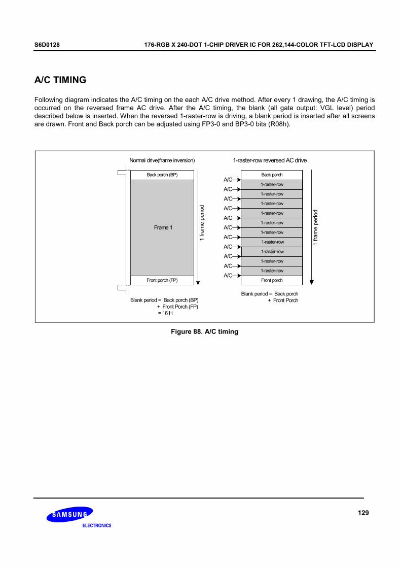
S6D0128 176-RGB X 240-DOT 1-CHIP DRIVER IC FOR 262,144-COLOR TFT-LCD DISPLAY
129
A/C TIMING
Following diagram indicates the A/C timing on the each A/C drive method. After every 1 drawing, the A/C timing is
occurred on the reversed frame AC drive. After the A/C timing, the blank (all gate output: VGL level) period
described below is inserted. When the reversed 1-raster-row is driving, a blank period is inserted after all screens
are drawn. Front and Back porch can be adjusted using FP3-0 and BP3-0 bits (R08h).
Frame 1
Normal drive(frame inversion)
1frameperiod
Blank period = Back porch (BP)
+ Front Porch (FP)
= 16 H
Front porch (FP)
Back porch (BP)
1-raster-row reversed AC drive
A/C
1frameperiod
Front porch
Back porch
A/C
A/C
A/C
A/C
A/C
A/C
A/C
A/C
A/C
A/C
1-raster-row
Blank period = Back porch
+ Front Porch
1-raster-row
1-raster-row
1-raster-row
1-raster-row
1-raster-row
1-raster-row
1-raster-row
1-raster-row
1-raster-row
Figure 88. A/C timing
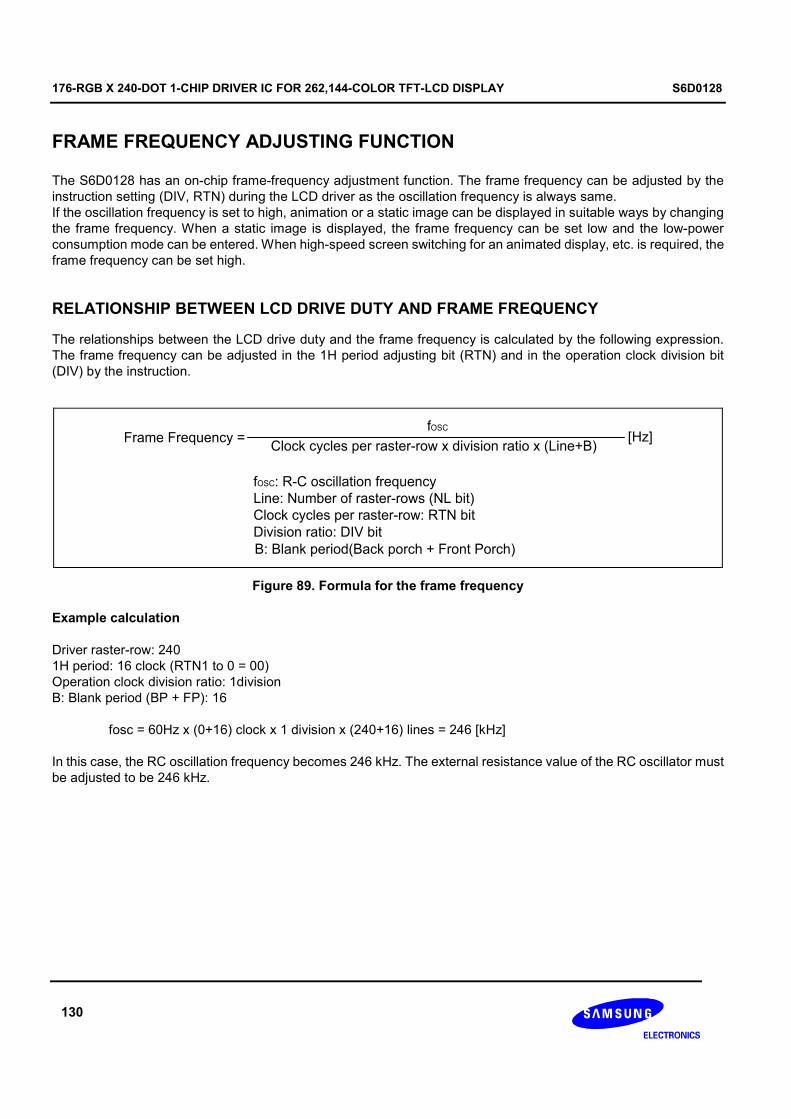
176-RGB X 240-DOT 1-CHIP DRIVER IC FOR 262,144-COLOR TFT-LCD DISPLAY S6D0128
130
FRAME FREQUENCY ADJUSTING FUNCTION
The S6D0128 has an on-chip frame-frequency adjustment function. The frame frequency can be adjusted by the
instruction setting (DIV, RTN) during the LCD driver as the oscillation frequency is always same.
If the oscillation frequency is set to high, animation or a static image can be displayed in suitable ways by changing
the frame frequency. When a static image is displayed, the frame frequency can be set low and the low-power
consumption mode can be entered. When high-speed screen switching for an animated display, etc. is required, the
frame frequency can be set high.
RELATIONSHIP BETWEEN LCD DRIVE DUTY AND FRAME FREQUENCY
The relationships between the LCD drive duty and the frame frequency is calculated by the following expression.
The frame frequency can be adjusted in the 1H period adjusting bit (RTN) and in the operation clock division bit
(DIV) by the instruction.
Frame Frequency =fOSC
Clock cycles per raster-row x division ratio x (Line+B)[Hz]
fOSC: R-C oscillation frequency
Line: Number of raster-rows (NL bit)
Clock cycles per raster-row: RTN bit
Division ratio: DIV bit
B: Blank period(Back porch + Front Porch)
Figure 89. Formula for the frame frequency
Example calculation
Driver raster-row: 240
1H period: 16 clock (RTN1 to 0 = 00)
Operation clock division ratio: 1division
B: Blank period (BP + FP): 16
fosc = 60Hz x (0+16) clock x 1 division x (240+16) lines = 246 [kHz]
In this case, the RC oscillation frequency becomes 246 kHz. The external resistance value of the RC oscillator must
be adjusted to be 246 kHz.

S6D0128 176-RGB X 240-DOT 1-CHIP DRIVER IC FOR 262,144-COLOR TFT-LCD DISPLAY
131
SCREEN-DIVISION DRIVING FUNCTION
The S6D0128 can select and drive two screens at any position with the screen-driving position registers (R14 and
R15). Any two screens required for display are selectively driven and reducing LCD-driving voltage and power
consumption.
For the 1st division screen, start line (SS17 to 10) and end line (SE17 to 10) are specified by the 1
st screen-driving
position register (R14). For the 2nd division screen, start line (SS27 to 20) and end line (SE27 to 20) are specified by
the 2nd screen-driving position register (R15). The 2
nd screen control is effective when the SPT bit is 1. The total
count of selection-driving lines for the 1st and 2
nd screens must correspond to the LCD-driving duty set value.
*
OCT 14th 0:18 am
G1
G7
G26
G42
1st screen :
7-raster-row driving
Non-display area
2nd screen:
17 raster-row driving
Non-display area
• Driving raster-row: NL4-0 = 11101 (240 lines)
• 1st screen setting: SS17-10 = 00H, SE17-10 = 06H• 2nd screen setting: SS27-20 = 19H, SE27-20 = 29H, SPT = 1
Rm
Figure 90. Driving on 2 screen

176-RGB X 240-DOT 1-CHIP DRIVER IC FOR 262,144-COLOR TFT-LCD DISPLAY S6D0128
132
RESTRICTION ON THE 1ST/2ND SCREEN DRIVING POSITION REGISTER SETTINGS
The following restrictions must be satisfied when setting the start line (SS17 to 10) and end line (SE17 to 10) of the
1st screen driving position register (R42H) and the start line (SS27 to 20) and end line (SE27 to 20) of the 2
nd screen
driving position register (R43H) for the S6D0128. Note that incorrect display may occur if the restrictions are not
satisfied.
Table 47. Restrictions on the 1st
/2nd
Screen Driving Position Register Setting
1st Screen Driving (SPT=0)
Register setting Display operation
(SE17 to 10) – (SS17 to 10) = NL Full screen display
Normally displays (SE17 to 10) to (SS17 to 10)
(SE17 to 10) – (SS17 to 10) < NL
Partial display
Normally displays (SE17 to 10) to (SS17 to 10)
White display for all other times (RAM data is not related
at all)
(SE17 to 10) – (SS17 to 10) > NL Setting disabled
NOTE 1: SS17 to 10 ≤ SE17 to 10 ≤ EFh
NOTE 2: Setting SE27 to 20 and SS27 to 20 are invalid
NOTE 3: SS17 + VL ≤ F0h
2nd Screen Driving (SPT=1)
Register setting Display operation
((SE17 to 10) – (SS17 to 10))
+ ((SE27 to 20) – (SS27-20)) = NL
Full screen display
Normally displays (SE27 to 20) to (SS17 to 10)
((SE17 to 10) – (SS17 to 10))
+ ((SE27 to 20) – (SS27-20)) < NL
Partial display
Normally displays (SE27 to 20) to (SS17 to 10)
White display for all other times (RAM data is not related
at all)
((SE17 to 10) – (SS17 to 10))
+ ((SE27 to 20) – (SS27-20)) > NL Setting disabled
NOTE 1: SS17 to 10 ≤ SE17 to 10 < SS27 to 20 ≤ SE27 to 20 ≤ EFh
NOTE 2: (SE27 to 20) – (SS17 to 10) ≤ NL
NOTE 3: SS17(SS27) + VL ≤ F0h
The driver output can’t be set for non-display area during the partial display. Determine based on specification of the
panels.
Source output in non-display area PT1 PT0
Positive polarity Negative polarity
Gate output in
Non-display area
0 0 AVSS AVSS Normal Scan
0 1 AVSS GVDD Normal Scan
1 0 GVDD AVSS Normal Scan
1 1 Hi-Z Hi-Z Normal Scan
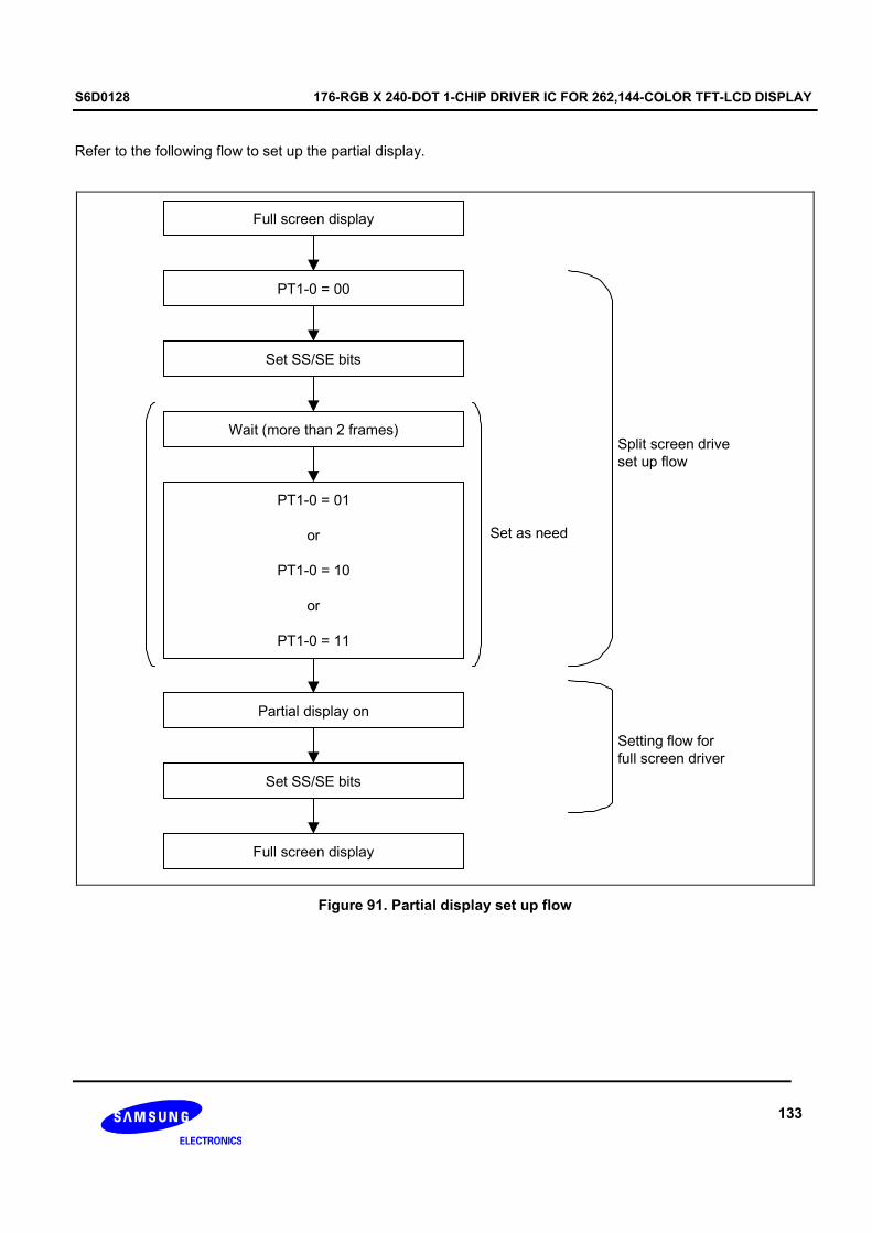
S6D0128 176-RGB X 240-DOT 1-CHIP DRIVER IC FOR 262,144-COLOR TFT-LCD DISPLAY
133
Refer to the following flow to set up the partial display.
Full screen display
PT1-0 = 00
Set SS/SE bits
Wait (more than 2 frames)
PT1-0 = 01
or
PT1-0 = 10
or
PT1-0 = 11
Partial display on
Set SS/SE bits
Full screen display
Set as need
Setting flow for
full screen driver
Split screen drive
set up flow
Figure 91. Partial display set up flow
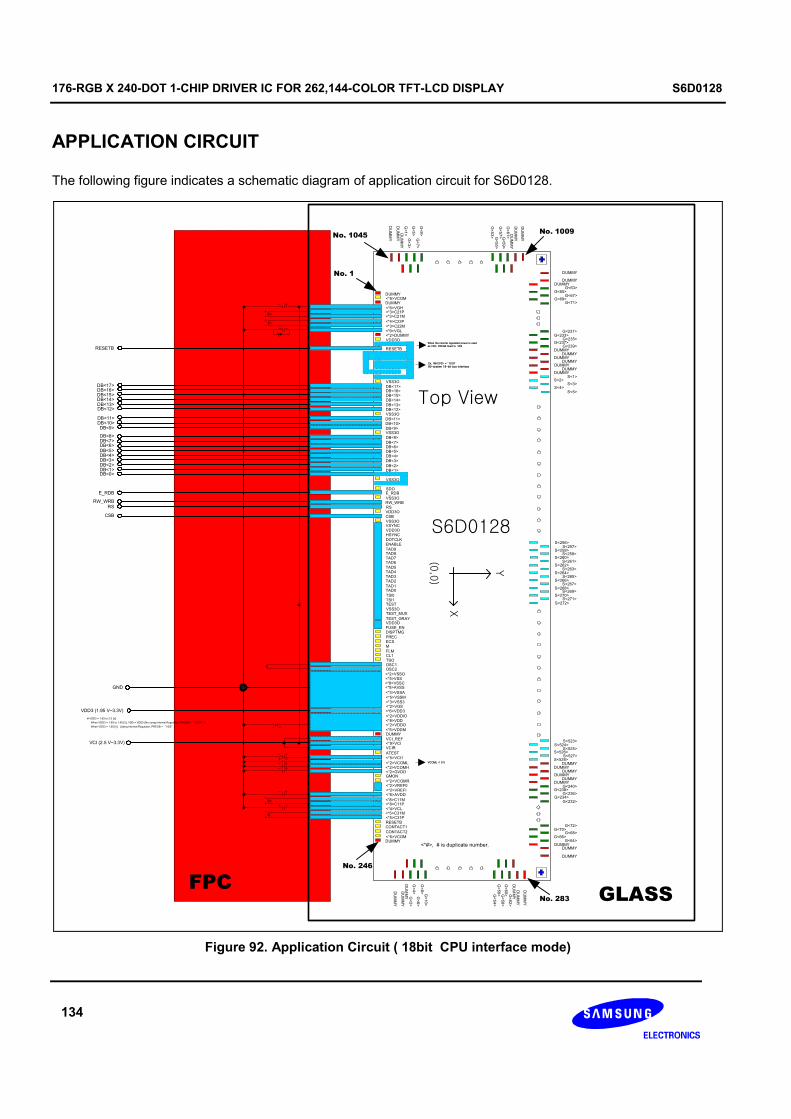
176-RGB X 240-DOT 1-CHIP DRIVER IC FOR 262,144-COLOR TFT-LCD DISPLAY S6D0128
134
APPLICATION CIRCUIT
The following figure indicates a schematic diagram of application circuit for S6D0128.
+-+- + -
- +
- +
+-
+-
- +- ++ -
- +
+ -
- +
GLASSFPC
S6D0128
No. 1
No. 246
No. 283
No. 1009No. 1045
DUMMY<*6>VCOM
<*6>VGH<*3>C21P<*3>C21M
<*4>C22P
<*3>C22M<*9>VGL<*2>DUMMYVDD3OPREGB
<*9>VCI
<*5>VCI1
<*8>C11P<*8>C11M
<*4>VCL
<*6>VDD3
<*2>VDDIO<*8>VDD<*2>VDDO
<*5>VDDM
GMON
VSS3OIM<0>
IM<1>
VDD3OIM<2>
IM<3>
<*8>AVSS
VSS3O
<*3>VSSA
RESETB
<*5>VSSM
<*5>VSS<*2>VSSO
<*8>VSSC
<*2>VGS
DB<17>DB<16>DB<15>
DB<14>
DB<13>DB<12>
DB<11>DB<10>
DB<9>
DB<8>
DB<7>DB<6>DB<5>
DB<3>
DB<2>DB<1>DB<0>
E_RDB
RW_WRBRS
CSB
VSYNC
HSYNC
DOTCLKENABLE
TAD9TAD8TAD7TAD6
TAD5TAD4TAD3TAD2
TAD1TAD0
VSS3OTEST_MUX
TEST_GRAYVDD3O
DISPTMG
PRECECSM
FLMCL1
TSOOSC1OSC2
DUMMY
<*6>VCOM
<*2>VREF0<*2>VREFI
RESETBCONTACT1
CONTACT2
DUMMY
VCI_REF
<*2>VCOML<*2>VCOMH<*2>GVDD
<*2>VCOMR
DUMMY
VCIR
Top View
Y
X
(0,0
)
VSS3O
VSS3O
VSS3OSDI
SDO
VSS3O
VSS3O
VDD3O
DB<4>
TSI0TSI1TEST
FUSE_EN
<*3>VSS3
ATEST
<*6>AVDD
<*5>C31P<*5>C31M
DUMMY
DUMMY
DUMMY G<2>
G<4>G<6>
G<8> G<10>
DUMMY
G<54>
G<56> G<58>
G<60> G<62>
DUMMY
DUMMY
G<64>DUMMY
DUMMY
DUMMY
G<68>G<66>
G<72>G<70>
G<236>G<234>
G<232>
G<240>G<238>
DUMMYDUMMY
DUMMYDUMMY
DUMMYDUMMY
S<527>S<528>
S<525>S<526>
S<523>S<524>
S<270>S<271>
S<272>
S<268>S<269>
S<266>S<267>
S<264>S<265>
S<262>S<263>
S<260>S<261>
S<258>S<259>
S<256>S<257>
S<3>S<4>
S<5>
S<1>S<2>
DUMMYDUMMY
DUMMYDUMMY
DUMMYDUMMY
G<239>DUMMY
G<235>G<237>
G<231>G<233>
G<71>
G<67>G<69>
G<63>G<65>
DUMMYDUMMY
DUMMYDUMMY
G<53> G<55>
G<57> G<59>
G<61>
DUMMY
DUMMY
DUMMY
DUMMY
DUMMY
G<1>G<3>
G<5>G<7>
G<9>
<*#>, # is duplicate number.
DB<17>DB<16>DB<15>DB<14>DB<13>DB<12>
DB<11>DB<10>
DB<8>DB<7>DB<6>DB<5>DB<4>DB<3>DB<2>DB<1>
E_RDB
RW_WRBRS
CSB
DB<9>
DB<0>
VDD3O
When the internal regulated power is used
as VDD, PREGB fixed to VSS
Ex. IM<3:0> = ‘1010’80-system 18-bit bus interface
RESETB
VCOML < 0 V
GND
VDD3 (1.95 V~3.3V)
VCI (2.5 V~3.3V)
# VDD3 = 1.65 to 3.3 [V]
When VDD3 = 1.65 to 1.95 [V], VDD = VDD3 (No using Internal Regulator, PREGB = “VDD3”)
When VDD3 > 1.95 [V] (Using Internal Regulator, PREGB = “VSS”)
Figure 92. Application Circuit ( 18bit CPU interface mode)

S6D0128 176-RGB X 240-DOT 1-CHIP DRIVER IC FOR 262,144-COLOR TFT-LCD DISPLAY
135
SPECIFICATIONS
ABSOLUTE MAXIMUM RATINGS
Table 48. Absolute Maximum Rating
(VSS = 0V)
Item Symbol Rating Unit
Supply voltage for Logic Block VDD – VSS -0.3 ~ 3.5 V
Supply voltage for I/O Block VDD3 – VSS -0.3 ~ 5.0 V
Supply voltage for step-up circuit VCI – VSS -0.3 ~ 5.0 V
AVDD - VSS -0.3 ~ 6.5 V
VSS - VCL -0.3 ~ 5.0 V LCD Supply Voltage range
|VGH – VGL| -0.3 ~ 35 V
Input Voltage range Vin -0.3 to VDD3 + 0.3 V
Operating temperature Topr -40 ~ 85 °C
Storage temperature Tstg -55 ~ 110 °C
Notes:
1. Absolute maximum rating is the limit value beyond which the IC may be broken. They do not assure operations.
2. Operating temperature is the range of device-operating temperature. They do not guarantee chip performance.
3. Absolute maximum rating is guaranteed when our company’s package used.

176-RGB X 240-DOT 1-CHIP DRIVER IC FOR 262,144-COLOR TFT-LCD DISPLAY S6D0128
136
DC CHARACTERISTICS
Table 49. DC Characteristics
(VSS = 0V)
Characteristic Symbol CONDITION MIN TYP MAX Unit Note
VDD 1.65 1.8 1.95 V *1 Operating voltage
VDD3 1.65 - 3.3 V *0, *1
VGH 7.0 - 16.5 V
VGL -13.75 - -3.5 V
VCL -2.75 - -1.75 V
AVDD 4.0 - 5.5 V
LCD driving voltage
GVDD 3.5 - 5.0 V
Input high voltage VIH 0.8*VDD3 VDD3 *2
Input low voltage VIL 0.0 0.2*VDD3 *2
Output high voltage VOH IOH = -0.5mA 0.7*VDD3 VDD3 *3
Output low voltage VOL IOL = 0.5mA 0.0 - 0.3*VDD3 *3
Input leakage current IIL VIN = VSS or VDD3 -1.0 1.0 *2
Output leakage current IOL VIN = VSS or VDD3 -3.0 3.0 *3
Operating frequency fosc
Frame freq. = 60 Hz
Display line = 240
Temp. = 25°C
VDD = 1.8V
221.4 246 270.6 kHz *4
Internal reference power
supply voltage VCI 2.5 3.3 V
Internal generated logic
supply voltage RVDD 1.65 1.8 1.95 V
1st step-up output
efficiency AVDD ILOAD = 2.5 mA 90 95 100 %
2nd step-up output
efficiency VGH ILOAD = 0.2 mA 90 95 100 %
3rd step-up output
efficiency VGL ILOAD = 0.2 mA 90 95 100 %
4th step-up output
efficiency VCL ILOAD = 0.3 mA 90 95 100 %
Notes: 0. When VDD3 = 1.65 to 1.95 [V], VDD = VDD3 (No using Internal Regulator, PREGB = “VDD3”)
When VDD3 > 1.95 [V] (Using Internal Regulator, PREGB = “VSS”)
1. VSS = 0V. 2. Applied pins; IM3-0, CSB, E_RDB, RW_WRB, RS, DB0 to DB17, RESETB. 3. Applied pins; DB0 to DB17 4. Target frame frequency = 60 Hz, Display line = 240, Back porch = 8, Front porch = 8
RTN1-0 = “00”, DIV1-0 = “00”
(You can measure OSC2 (fosc) or CL1 (fosc / 16))
fosc range can be changed by module condition. The oscillation frequency is changed according to the
external resistance value, wiring length, or operating power-supply voltage.

S6D0128 176-RGB X 240-DOT 1-CHIP DRIVER IC FOR 262,144-COLOR TFT-LCD DISPLAY
137
Table 50. DC Characteristics for LCD driver outputs
(VDD = 1.8V, VDD3 = 3.0V, VSS = 0V)
Characteristic Symbol CONDITION MIN TYP MAX Unit Note
LCD gate driver output
On resistance Ron
VGH–VGL=30V,
VGH=16.5V,
VGL=-13.5V
- - 2
4.2V ≤ Vso - ±20 ±50 mV *5
0.8V < Vso < 4.2V - ±10 ±25 mV *5 Output voltage deviation
(Mean value) ∆Vo
Vso ≤ 0.8V - ±20 ±50 mV *5
AVDD = 5.5V
GVDD = 5.0V
SAP = “010”
Ta = 25 °C
- - 86 us *6
AVDD = 5.5V
GVDD = 5.0V
SAP = “011”
Ta = 25 °C
- - 57 us *6
AVDD = 5.5V
GVDD = 5.0V
SAP = “100”
Ta = 25 °C
- - 40 us *6
LCD source driver delay tSD
AVDD = 5.5V
GVDD = 5.0V
SAP = “101”
Ta = 25 °C
- - 34 us *6
IVDD - - 100 uA Current consumption
during normal operation IVCI
No load,
Ta = 25 °C - - 3 mA
Notes :
5. Vso the output voltage of analog output pins S1 to S528
6. tSD : LCD Source driver delay
tSD = 1 / [Frame Freq. x The number of raster-row + The number of blank period (FP+BP)]
– The marginal time for pixel load charge
Figure 93. LCD Source driver delay

176-RGB X 240-DOT 1-CHIP DRIVER IC FOR 262,144-COLOR TFT-LCD DISPLAY S6D0128
138
AC CHARACTERISTICS
Table 51. Parallel Write Interface Characteristics (68 Mode)
(VDD = 1.8V, VDD3 = 1.65 to 3.3V, TA = -40 to +85oC)
Specification Characteristic Symbol
Min. Max. Unit
Write tCYCW68 100 - Cycle time
Read tCYCR68 500 -
Pulse rise / fall time tR, tF - 25
Write tWHW68 40 - E pulse width high
Read tWHR68 250 -
Write tWLW68 40 - E pulse width low
Read tWLR68 200 -
RW, RS and CSB setup time tAS68 10 -
RW, RS and CSB hold time tAH68 2 -
Write data setup time tWDS68 60 -
Write data hold time tWDH68 15 -
Read data delay time tRDD68 - 200
Read data hold time tRDH68 5 -
ns

S6D0128 176-RGB X 240-DOT 1-CHIP DRIVER IC FOR 262,144-COLOR TFT-LCD DISPLAY
139
RW_WRB VIL VIL
VIH
VIL
VIH
VIL
VOH1
VOL1
VOH1
VOL1
VIL VIL
VIL VIL
VIH
VIH
VIH
VIH
VIL
tCYCW68
/tCYCR68
tR tF
tWHW68
/tWHR68
tWLW68/
tWLR68
tAS68 tAH68
tWDS68tWDH68
tRDH68tRDD68
RS
CSB
E_RDB
DB17~0
DB17~0
WRITE DATA
READ DATA
Figure 94. AC characteristics (68 Mode)

176-RGB X 240-DOT 1-CHIP DRIVER IC FOR 262,144-COLOR TFT-LCD DISPLAY S6D0128
140
Table 52. Parallel Write Interface Characteristics (80 Mode)
(VDD = 1.8V, VDD3 = 1.65 to 3.3V, TA = -40 to +85oC)
Specification Characteristic Symbol
Min. Max. Unit
Write tCYCW80 100 - Cycle time
Read tCYCR80 500 -
Pulse rise / fall time tR, tF - 25
Write tWLW80 40 - Pulse width low
Read tWLR80 250 -
Write tWHW80 40 - Pulse width high
Read tWHR80 200 -
RW, RS and CSB setup time tAS80 10 -
RW, RS and CSB hold time tAH80 2 -
Write data setup time tWDS80 60 -
Write data hold time tWDH80 15 -
Read data delay time tRDD80 - 200
Read data hold time tRDH80 5 -
ns

S6D0128 176-RGB X 240-DOT 1-CHIP DRIVER IC FOR 262,144-COLOR TFT-LCD DISPLAY
141
WRITE DATA
READ DATA
VIL VIL
VIH
VIL
VIH
VIL
VOH1
VOL1
VOH1
VOL1
VIL VIL
VIL
VIH
VIH
VIH
VIH
tCYCW80
/tCYCR80
tR tF
tWLW80/
tWLR80
tWHW80
/tWHR80
tAS80 tAH80
tWDS80tWDH80
tRDH80tRDD80
RS
CSB
/RD
DB17~0
DB17~0
VIH
VIL
/WR
Figure 95. AC characteristics (80 Mode)

176-RGB X 240-DOT 1-CHIP DRIVER IC FOR 262,144-COLOR TFT-LCD DISPLAY S6D0128
142
Table 53. Clock Synchronized Serial Write Mode Characteristics
(VDD = 1.8V, VDD3 = 1.65 to 3.3V, TA = -40 to +85oC)
specification Characteristic Symbol
Min. Max. Unit
Serial clock cycle time tscyc 250 - ns
Serial clock rise / fall time tR, tF - 25 ns
Pulse width high for write tSCHW 40 - ns
Pulse width high for read tSCHR 230 - ns
Pulse width low for write tSCLW 60 - ns
Pulse width low for read tSCLR 230 - ns
Chip Select setup time tCSS 20 - ns
Chip Select hold time tCSH 60 - ns
Serial input data setup time tSIDS 30 - ns
Serial input data hold time tSIDH 30 - ns
Serial output data delay time tSODD - 130 ns
Serial output data hold time tSODH 5 - ns
Table 54. Reset Timing Characteristics
(VDD = 1.8V, VDD3 = 1.65 to 3.3V, TA = -40 to +85oC)
Characteristic Symbol Min. Max. Unit
Reset low pulse width tRES 1 - us

S6D0128 176-RGB X 240-DOT 1-CHIP DRIVER IC FOR 262,144-COLOR TFT-LCD DISPLAY
143
Transfer Start
VOH1
VOL1
VIL
VIH
VIL
VOH1
VOL1
VIH
tSIDS tSIDH
tSODH
SCL
SDI
SDO
VIL VIL
VIH VIH
VIL VIL
VIH VIH
CSB
VIH
VIL
tSODD
tCSS tCSHtR tF
tSCHW /
tSCHR
tSCLW /
tSCLR
tscyc
INPUT DATAINPUT
DATA
OUTPUT DATAOUTPUT
DATA
Transfer End
Figure 96. AC characteristics (SPI Mode)
tRES
RESETBVIL VIL
Figure 97. AC characteristics (RESET timing)

176-RGB X 240-DOT 1-CHIP DRIVER IC FOR 262,144-COLOR TFT-LCD DISPLAY S6D0128
144
Table 55. RGB Data Interface Characteristics
(VDD = 1.8V, VDD3 = 1.65 to 3.3V, TA = -40 to +85oC)
18/16bit RGB interface 6bit RGB interface Characteristic Symbol
Min. Max. Min. Max. Unit
DOTCLK cycle time tDCYC 100 - 100 -
DOTCLK rise / fall time tR, tF - 25 25
DOTCLK Pulse width high tDCHW 40 - 40 -
DOTCLK Pulse width low tDCLW 40 - 40 -
ENABLE setup time tENS 30 - 30 -
ENABLE hold time tENH 20 - 20 -
DB data setup time tPDS 30 - 30 -
DB data hold time tPDH 20 - 20 -
ns
VI
H
VI
L
VIH
tPDS tPDH
DOTCLK
DB[17:0]
VIL
VIH
VIL VIL
VIH
ENABLE
VI
H
VI
L
tENHtR tFtDCHW tDCLW
tDCYC
DB[17:0] DB[17:0]
tENS
VIL
VIH
VIH
Figure 98. AC characteristics (RGB Mode)

S6D0128 176-RGB X 240-DOT 1-CHIP DRIVER IC FOR 262,144-COLOR TFT-LCD DISPLAY
145
REVISION HISTORY
Version Content Author Date
0.0 Original S.H.LIM March 31. 2005
0.1
Page 8
- Added PAD Configuration (figure 2)
Page 9
- Added S6D0128 PAD Dimension
Page 10
- Added Align Key
Page 11 ~ 17
- Added PAD Center Coordinates
S.H.LIM May 17. 2005
Page 8, 11
- Changed PAD name from “TSO0” to “TSO”
Page 23
- Added Description “VCIR” Pin for test.
Page 23
- Added Description “ATEST” Pin for test.
Page 80
- Deleted diode between VGL and VCL in figure 28
S.H.LIM May 27. 2005
0.2
Page 6
- Changed operating Voltage range (VDD, VDD3) in Features
Page 18
- Inserted VDD comment “connected to VDDM”
in regulated mode
- Inserted VDDM comment “VDDM connected to VDD3”
in Non-regulated mode
- Inserted VDDM comment “VDDM is regulator output “
in regulated mode
- Inserted VDD3 comment “VDD3 is more than VDD” in VDD3
pin description
- Changed VDD3 comment in VDD3 pin description
Page 50
- Added comment “3. Case of Blank display “
Page 84
- Changed VDD3 range in figure 33
Page 139
- Changed VDD3 range from “1.8~3.3V” to “1.65~3.3V” in
table50
- Inserted Note 0 (VDD3 comment)
Page 141 ~ 147
- Changed VDD3 range from “1.8~3.3V” to “1.65~3.3V” in AC
Characteristics
Page 6,60,61,80,81,139
- Changed GVDD range from “3.0 to 5.0V” to “3.5 to 5.0V”
- Changed AVDD range from “3.5 to 5.5V” to “4.0 to 5.5V”
Page 138
- Added Application Circuit
S.H.LIM July 19. 2005
176-RGB X 240-DOT 1-CHIP DRIVER IC FOR 262,144-COLOR TFT-LCD DISPLAY S6D0128
146
Version Content Author Date
1.0 Page 29~32,34~37
- Changed from “GRAM_DATA” to INPUT_DATA”
Page 40,41 Changed column R/W of the Instruction Table
- Changed from 0 to W
- Changed from 1 to R
Page 40, 45, 80, 110, 131
- Deleted 3 Field-interlace function.
Page 40, 45, 48, 100 ..
- Deleted AM register in R03H instruction
Page 48
- Added BGR Description
Page 50 Changed REV Description
- Changed from 18’h00000 to 6’b000000
- Changed from 18’h3FFFF to 6’b111111
Page 70
- Deleted the table of “GRAM Data and Grayscale level “
- Added Memory data write sequence
Page 74
- Modified GRAM read sequence
Page 76
- Added Note “Number of LCD driver lines + Scanning start
position < 241 “
Page 82
- Move Instruction setup flow from 128 page to 82 page
- Modified setup flow of power
(Added “wait more than 1frame” and “wait time about PON off ,
PON1 off”)
Page 84
- Modified title from “Instruction setup flow “ to “Setup flow of
display”
Page136
-Added Schottky diode between VGH and VCI in Application
Circuit
Page 137
- Changed Absolute Maximum Ratings
Page 138
- Added MIN & MAX value of operating frequency
- Added Temp. & VDD condition of operating frequency
Page 138
- Changed 1st step-up output efficiency condition
Page 138
- Changed 2nd step-up output efficiency condition
Page 138
- Changed 3rd step-up output efficiency condition
Page 139
- Changed LCD source driver delay
- Added tSD Description
- Changed Current consumption value from TYP to MAX
S.H.YUO
S.H.LIM November 2 . 2005
S6D0128 176-RGB X 240-DOT 1-CHIP DRIVER IC FOR 262,144-COLOR TFT-LCD DISPLAY
147
NOTICE
Precautions for Light
Light has characteristics to move electrons in the integrated circuitry of semiconductors, therefore may change
the characteristics of semiconductor devices when irradiated with light. Consequently, the users of the packages
which may expose chips to external light such as COB, COG, TCP and COF must consider effective methods to
block out light from reaching the IC on all parts of the surface area, the top, bottom and the sides of the chip.
Follow the precautions below when using the products.
1. Consider and verify the protection of penetrating light to the IC at substrate (board or glass) or product design
stage.
2. Always test and inspect products under the environment with no penetration of light.


