Download - Copyright by Kha Xuan Tran 2019

Copyright
by
Kha Xuan Tran
2019
The Dissertation Committee for Kha Xuan Tran Certifies that this is the approved version
of the following disseration
Exciton and Valley Properties in Atomically Thin Semiconductors and
Heterostructures
Committee
Xiaoqin Li Supervisor
Chih-Kang Shih
Ananth Dodabalapur
Keji Lai
Nanshu Lu
Exciton and Valley Properties in Atomically Thin Semiconductors and
Heterostructures
by
Kha Xuan Tran
Dissertation
Presented to the Faculty of the Graduate School of
The University of Texas at Austin
in Partial Fulfillment
of the Requirements
for the Degree of
Doctor of Philosophy
The University of Texas at Austin
May 2019
Dedication
Dedicate to my parents family and friends
v
Acknowledgements
Six years ago in summer 2013 I arrived in Austin Texas eager to start a new journey of
earning a PhD in physics Looking back at the time I spent at The University of Texas at
Austin there are certainly many challenges as well as many fond memories I am grateful for the
opportunity to study and work here with a lot of hardworking people
First of all I would like to thank my supervisor professor Xiaoqin Elaine Li Although
she is a tough mentor with a lot of demands to her students she cares about her students success
Ultimately her knowledge determination and perseverance have shown me that I can achieve
goals that I thought were never possible
Members of the Li group were fun to work with Akshay Singh helped me a great deal
when I first joined the group He has patiently taught me how to operate instruments in the lab
and how to run the pump-probe setup We had many engaging and stimulating scientific
discussions as well as conversations about not too important things Kai Hao and Liuyang Sun
helped me with tips and tricks about setting up optics and troubleshooting problems from time to
time I especially enjoy discussing the sample fabricating process with Junho Choi and Jiamin
Quan They often have great ideas on how to improve the sample making process to achieve
better quality samples Last but not least I would like to thank Li group undergraduate team
Andreacute Zepeda and Marshall Campbell have stayed in the lab very late with me trying to finish
making a TMD heterostructure Matt Staab Kayleigh Jones Carter Young Dennis Hong
Eduardo Priego Tiffany Pham-Nguyen Samantha Smith Michael Alexopoulos all provided
helps with exfoliating monolayers for my samples Jacob Embley who is taking over the setup
vi
after I leave was fun to work with I hope that I have left a decently working lab behind for him
to continue his PhD
I am also very grateful to work with a lot of excellent collaborators in the field Galan
Moody provides help with writing and scientific knowledge Fengcheng Wu and professor Allan
MacDonald provide theory support for my experiment Xiaobo Lu and professor Li Yang
provide band structure calculations that further consolidate my experimental results
In the end I thank my parents Theyve provided me advice support and encouragement
throughout my entire academic career
vii
Exciton and Valley Properties in Atomically Thin Semiconductors and
Heterostructures
Kha Xuan Tran PhD
The University of Texas at Austin 2019
Supervisor Xiaoqin Elaine Li
Two dimensional van der Waals (vdW) materials recently emerged as promising
candidates for optoelectronic photonic and valleytronic applications Monolayer transition
metal dichalcogenides (TMD) are semiconductors with a band gap in the visible frequency range
of the electromagnetic spectrum Their unique properties include evolution from indirect band
gap in bulk materials to direct band gap in monolayers large exciton binding energy (few
hundred meV) large absorption per monolayer (about 10) strong spin-orbit coupling and
spin-valley locking Moreover two or more TMD monolayers can be stacked on top of one
another to create vdW heterostructures with exciting new properties
Optical properties of semiconductors near the band gap are often dominated by the
fundamental optical excitation the exciton (Coulomb-bound electron-hole pair) Excitons in
TMD monolayers (intralayer exciton) exhibit a large binding energy and a very short lifetime
The excitons in TMD monolayers are formed at the boundary of the Brillouin zone at the K and
viii
K points The time-reversal symmetry dictates that spins are oriented with opposite directions
leading to distinct optical selection rules for the excitons at these two valleys a property known
as the spin-valley locking Valley polarization is often characterized by circularly polarized
photoluminescence (PL) We show that the degree of valley polarization in a WSe2 monolayer
depends on the degree of disorder evaluated by the Stokes shift between the PL and absorption
spectra Intrinsic valley dynamics associated with different optical resonances can only be
evaluated using resonant nonlinear optical spectroscopy We discovered exceptionally long-lived
intra-valley trions in WSe2 monolayers using two-color polarization resolved pump-probe
spectroscopy
A different type of excitons (interlayer excitons) may rapidly form in TMD
heterostructures with a type-II band alignment Because of the spatial indirect nature interlayer
excitons have a much longer lifetime which is tunable by the twist angle between the two layers
Especially we discover that multiple interlayer excitons formed in a small twist angle
heterobilayer exhibit alternating circular polarization - a feature uniquely pointing to Moireacute
potential as the origin We assign these peaks to the ground state and excited state excitons
localized in a Moireacute potential and explain how the spatial variation of optical selection rule
within the moireacute superlattice can give rise to multiple peaks with alternative circular polarization
The twist angle dependence recombination dynamics and temperature dependence of these
interlayer exciton resonances all agree with the localized exciton picture Our results suggest the
feasibility of engineering artificial excitonic crystal using vdW heterostructures for
nanophotonics and quantum information applications
ix
Table of Contents
List of tables xi
List of figures xii
Chapter 1 Introduction and overview 1
I Definition of semiconductor 1
II Early experiments on semiconductor 2
III From vacuum tube to transistor 4
IV Some concepts and ideas of band theory 6
Chapter 2 Introduction to monolayer transition metal dichalcogenides (TMDs) 10
I TMD lattice structure and polymorphs 10
II Evolution from indirect band gap in bulk material to direct band gap in
monolayer 12
III Excitons13
IVK-K valleys in monolayer TMD 19
V Dark excitons 20
VI Valley property of excitonic states (ie exciton trion) 23
VII Trions28
Chapter 3 Introduction to TMD heterostructures 33
I TMD heterobilayer band alignment and optical properties 33
II Moireacute pattern in TMD heterobilayer 36
Chapter 4 Experimental Techniques 39
I Photoluminescence 39
II White light absorption measurement41
III Pump probe spectroscopy 42
x
IV Second harmonic generation (SHG) techniques 53
Chapter 5 Steady state valley properties and valley dynamics of monolayer TMD 61
I Disorder dependent valley properties in monolayer WSe2 61
II Long lived valley polarization of intravalley trions in monolayer WSe2 76
Chapter 6 Evidence for Moireacute excitons in van der Waal heterostructure 89
I Motivation 89
II Moireacute theory overview 91
III Sample details and experimental methods 94
IV Moireacute exciton model 97
V First principles calculation of the bandgaps of MoSe2-WSe2 bilayer
heterostructure101
VI Thermal behavior and recombination dynamics103
VII Additional heterostructures 105
VIII PL emission from Sz = 1 and Sz = 0 exciton transitions 107
IX Conclusion 108
Chapter 7 Conclusion and outlook110
Appendix Sample fabrication techniques 113
I Exfoliation 113
II Transfer 119
III Encapsulated heterostructure fabrication 126
IV Atomic Force Microscope (AFM) images of the fabricated sample 131
References 134
xi
List of tables
Table 61 Summary of peak positions full-width half-maximum (FWHM) and Stokes Shift
(SS) using Lorentzian (L) Gaussian (G) and Half-gaussian fitting methods for different
samples 71
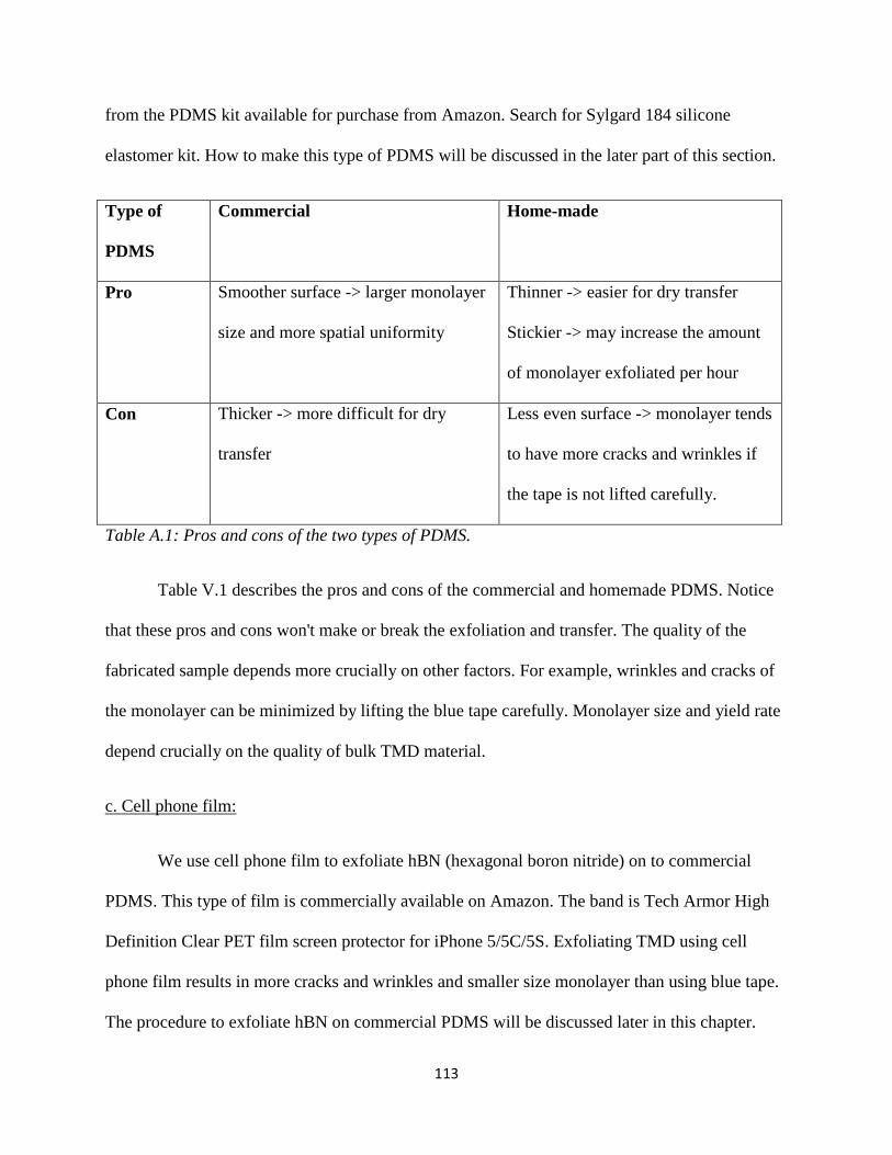
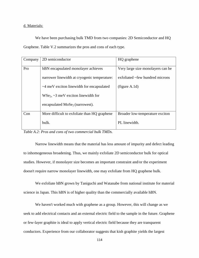
Table A1 Pros and cons of the two types of PDMS 114
Table A2 Pros and cons of two commercial bulk TMDs 115
xii
List of Figures
Figure 11 Comparison of electrical conductivities of insulators metals and semiconductors
2
Figure 12 First semiconductor diode the cats whisker detector used in crystal radio Source
wikipedia 3
Figure 13 a) Schematic of the vacuum tube that only permits electricity to flow in one
direction Electrons can flow from hot cathode to anode but not the other way
around b) Metal grid inserted in the space between the anode and cathode can
control the current flow between anode and cathode Source wikipedia 5
Figure 14 Top views of probability density plots for an electron in hydrogen atom Brighter
area corresponds to region with higher probability of finding the electron 7
Figure 15 Energy band gaps for (a) metal -- zero energy gap (b) semiconductor -- 1 to 2 eV
gap (c) insulator -- larger than 3 eV gap 8
Figure 16 In a direct (indirect) bandgap material the CB minimum and the VB maximum
occur at the same (different) position in momentum space as illustrated in panel a
( panel b) 9
Figure 21 Two main structure polymorphs of TMD 2H trigonal prismatic and 1T
octahedral The crimson (gray) circle represents chalcogen(metal) atom The red
(gray) shadow represents primitive (computational) cell 12
Figure 22 a) The Brillouin zone of monolayer TMD showing the path in which the band
structure is drawn in part b b) Calculated band structure of bulk and 1 layer
MoS2 The solid arrows indicate the lowest energy transitions Bulk (1 layer) has
indirect (direct) bandgap c) PL measurement with different layers 1 layer MoS2
has much higher luminescence than 2 layer MoS2 13
xiii
Figure 23 a) Schematic of real space representation of an exciton b) The modulus squared of
the electron wave function of an exciton in which the hole position is fixed at the
center black circle The inset shows the corresponding wave function in
momentum space across the Brillouin zone Figure adapted from ref [6] c)
Representation of the exciton in reciprocal space d) Dispersion curve for the
exciton with different excited states in a direct band gap semiconductor with
energy gap Eg and exciton bind energy EB labeled e) Exciton series measured in
the absorption spectrum of a multi-layer MoS2 Figure adapted from ref [14] f)
Derivative of the reflectance contrast spectrum of a monolayer WS2 showing the
emergence of higher excited exciton states 16
Figure 24 a) Schematic represents exciton in 3D (bulk) and 2D (monolayer) TMD b) The
effect of increased binding energy in 2D system due to reduced dielectric
screening The binding energy is indicated by the dash red double arrows Figure
adapted from ref [5] c) Logarithm of a typical dIdV curve obtained from
scanning tunneling microscopy measurement of monolayer MoSe2 used to obtain
band gap value 18
Figure 25 a) The Brillouin zone of monolayer TMD with the reciprocal lattice vectors b1
b2 b) Band structure of monolayer WSe2 around K and Krsquo points Exciton at K
and Krsquo valley couples to light with σ+ and σ- polarization respectively 20
Figure 26 Different types of dark excitons a) Spin forbidden dark exciton in
tungsten(molybdenum) based monolayer TMD denoted WX2 and MoX2
respectively b) Momentum indirect dark exciton in which electron and hole are
not in the same valley c) Momentum indirect dark exciton in which same valley
electron located outside of the light cone 22
Figure 27 a) The circular polarized photoluminescence spectrum of monolayer MoS2 at
14K The excitation energy is indicated by the arrow which is 196 eV b) The
circular polarized photoluminescence spectrum of monolayer WSe2 at 4K excited
with the same energy as part a) X0 and X
- denote the exciton and trion peak
respectively 25
Figure 28 a) The linear polarized PL of monolayer WSe2 at cryogenic temperature excited
with 188 eV CW laser Different gate voltages are used to control the emergence
of neutral exciton X0 negative trion X- and positive trion Co(cross) linear
detection is plotted as the black(red) curves b) Normalized neutral exciton
intensity peak as a function of detection polarization angles 27
xiv
Figure 29 a) Microscopic image of a monolayer MoSe2 and the two metal contact b) Device
schematic to control the doping level in the sample c) PL spectrum of the
monolayer as a function of gate voltage The labels are as followed X0 exciton
X- negative trion X
+ positive trion X
I impurity peak d) Contour plot of the first
derivative of the differential reflectivity in a charge tunable WSe2 monolayer
Double trion peaks emerge at the n-dope regime 30
Figure 210 Charge configuration of (a) intravalley trion (b) intervalley trion of monolayer
WSe2 and (c) intervalley trion of monolayer MoSe2 31
Figure 31 a) Type II band alignment of MoSe2-WSe2 heterobilayer The conduction band
minimum (valence band maximum) is belong to monolayer MoSe2(WSe2)
Charge transfer intra- and interlayer exciton recombination timescales are
indicated b) Band structure of the aligned TMD heterostructure at 0 degree
stacking angle Conduction band K(K) valley from MoSe2 is aligned with valence
band K(K) valley from WSe2 in momentum space c) The low temperature PL
spectrum of an aligned heterobilayer MoSe2-WSe2 featuring interlayer exciton
(IX) peak around 14 eV 35
Figure 32 a) Twist angle increasing makes the IX becoming indirect in momentum Optical
transition requires the participation of Δk momentum phonon Figure adapted
from ref [13] b) The PL intensity of IX decreases as the twist angle increase from
0o and increases again as the twist angle approaching 60
o c) Time resolved PL of
IX detected at 1320 meV for three samples with increasing twist angles showing
increased lifetime of IX for larger twist angle sample 36
Figure33 a) STM image of rotational aligned WSe2-MoS2 heterobilayer showing the moireacute
superlattice period of 87 nm b) Moireacute supercell with
denoting the
locations that retain the three fold symmetry c) Zoom in view showing the
specific atomic alignment d) and e) Layer separation and band gap variation of
the TMD moireacute pattern respectively 38
Figure 41 Schematic of the photoluminescencewhite light absorption optical setup 41
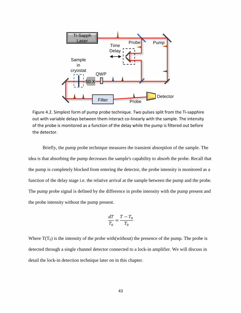
Figure 42 Simplest form of pump probe technique Two pulses split from the Ti-sapphire
out with variable delays between them interact co-linearly with the sample The
intensity of the probe is monitored as a function of the delay while the pump is
filtered out before the detector 43
xv
Figure 43 Two color pump probe optical setup In addition to the simple pump probe in the
previous figure the pulse shapers are inserted to independently vary the
wavelength or photon energy of two pulses 45
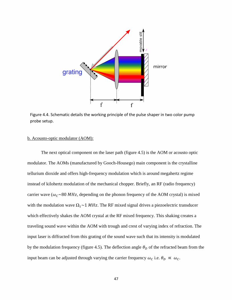
Figure 44 Schematic details the working principle of the pulse shaper in two color pump
probe setup 47
Figure 45 Schematic of the RF (radio frequency) generation and AOM (acousto-optic
modulator) 48
Figure 46 Schematic of lockin amplifier illustrating signal (S) and reference frequency (R)
convolution using the integrator 50
Figure 47 Schematic of the autocorrelation setup to measure the pulse duration 52
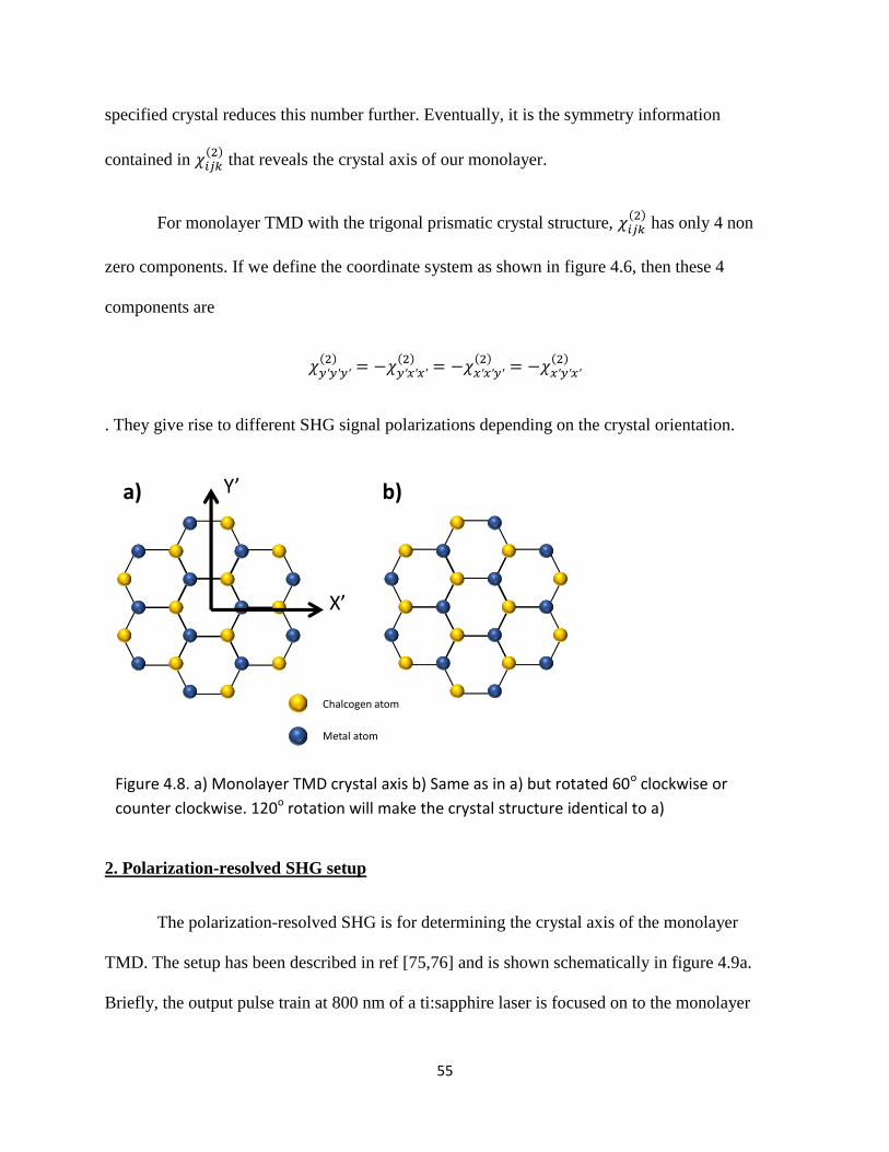
Figure 48 a) Monolayer TMD crystal axis b) Same as in a) but rotated 60o clockwise or
counter clockwise 120o rotation will make the crystal structure identical to a) 55
Figure 49 a) Schematic of the polarization resolved SHG setup b) SHG polarized intensity
as the sample is rotated 360o in the plane to which the laser beam is perpendicular
to 56
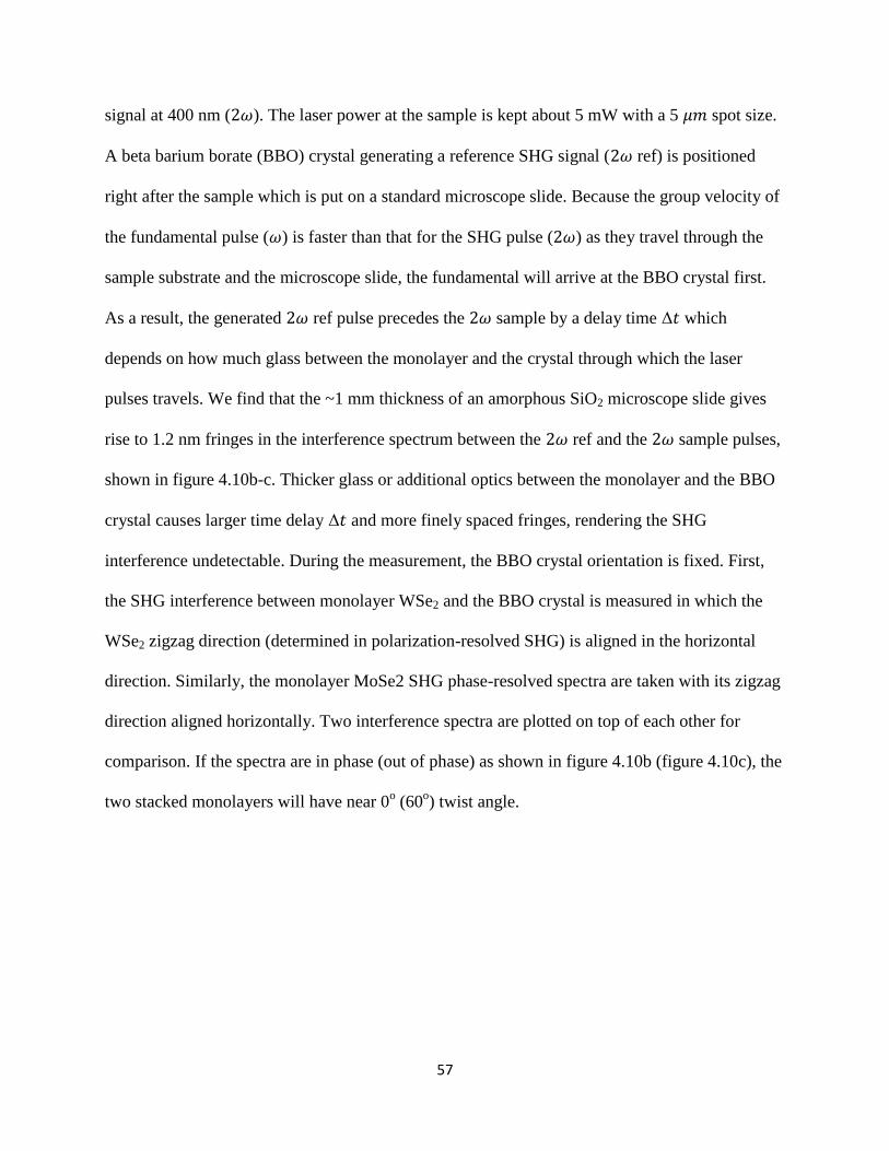
Figure 410 a) Schematic of the spectral phase resolved SHG setup b) SHG phase resolved
spectra between the monolayers and the BBO crystal with signal in phase for a
near twist angle stacking c) Similar to b) but with out-of-phase signals for a
near twist angle 58
Figure 411 Coordinate systems used in SHG signal calculation XOY is the lab frame of
reference in which OX(OY) is the horizontal(vertical) direction XOY is the
sample frame of reference in which OX(OY) is the armchair(zigzag) direction
Angle between OX and OX is 60
xvi
Figure 51 a) The band structure of monolayer WSe2 at two degenerate K and K valleys
Valley contrasting spins allow left (right) circular polarized light to excite
excitons in the K (K) valley b) Bloch Sphere representation of valley pseudospin
degree of freedom Circular polarized light prepares an exciton in |Kgt or |Kgt
state ie states at the poles whereas linear polarized light prepares an exciton in a
superposition of |Kgt and |Kgt ie states at the equator 63
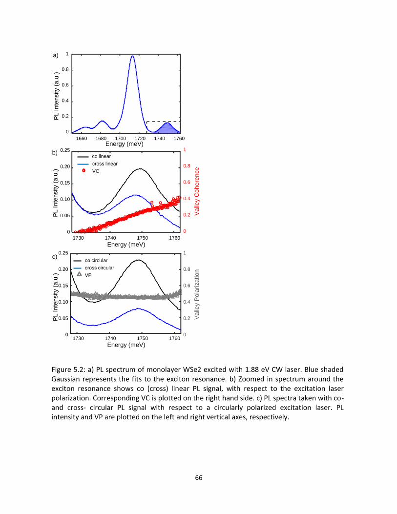
Figure 52 a) PL spectrum of monolayer WSe2 excited with 188 eV CW laser Blue shaded
Gaussian represents the fits to the exciton resonance b) Zoomed in spectrum
around the exciton resonance shows co (cross) linear PL signal with respect to
the excitation laser polarization Corresponding VC is plotted on the right hand
side c) PL spectra taken with co- and cross- circular PL signal with respect to a
circularly polarized excitation laser PL intensity and VP are plotted on the left
and right vertical axes respectively 66
Figure 53 a) Stoke shift is shown as the difference in energy between the absorption
spectrum and PL from the exciton resonance Inset SS dependence on
temperature b) VC (VP) is plotted with respect to SS VC shows an inverse
dependence versus SS whereas VP shows no recognizable trend 69
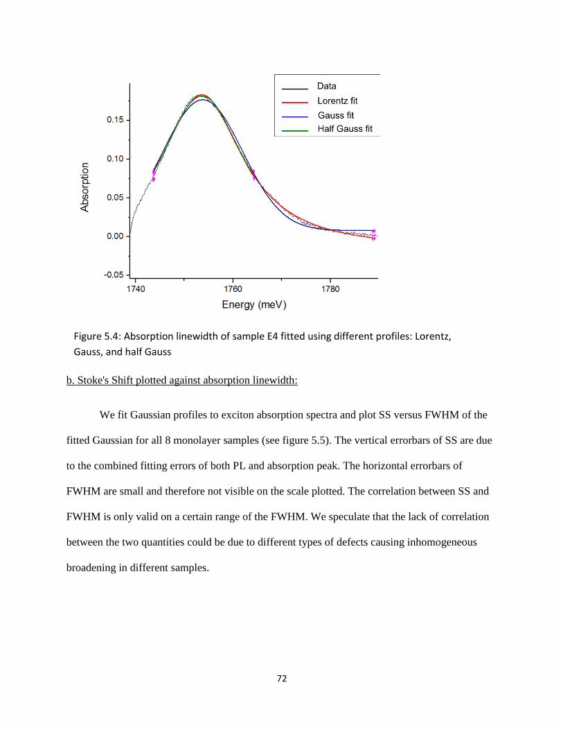
Figure 54 Absorption linewidth of sample E4 fitted using different profiles Lorentz Gauss
and half Gauss 72
Figure 55 The absorption spectra are fitted with Gaussian profile and the FWHMs are
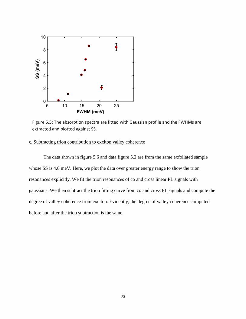
extracted and plotted against SS 73
Figure 56 a) Trion resonances on both co and cross signal are fitted with Gaussians Since
trion doesnt show any valley coherence the fits are essentially the same Valley
coherence is shown here before the trion subtraction from the co and cross
signals b) After trion subtraction the valley coherence is essentially the same
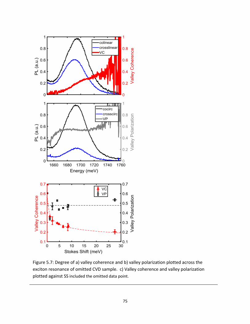
signifying that trion has minimal contribution to exciton valley coherence 74
Figure 57 Degree of a) valley coherence and b) valley polarization plotted across the exciton
resonance of omitted CVD sample c) Valley coherence and valley polarization
plotted against SS included the omitted data point 75
xvii
Figure 58 (a) Possible configurations of charged and neutral bright excitons in WSe2 (b)
Differential transmission spectrum of WSe2 (dots) The black line is an
interpolation curve serving as a guide to the eye The solid Gaussians illustrate
the spectral position of the exciton and the two trion (inter- and intravalley)
resonances The spectral positions of probe energies for data in figure 69 and
610 (dashed colored lines) and the pump energy for figure 610 (gray line) are
also illustrated 80
Figure 59 Co- (solid dots) and cross-polarized (open dots) signals recorded in resonant
excitation experiments across the trion resonance at probe energies of (a) 17268
meV (b) 1722 meV and (c) 17196 meV (d) Valley polarization for the
measurements displayed in (a) and (c) 84
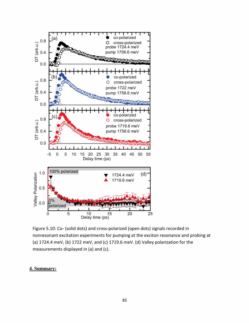
Figure 510 Co- (solid dots) and cross-polarized (open dots) signals recorded in nonresonant
excitation experiments for pumping at the exciton resonance and probing at (a)
17244 meV (b) 1722 meV and (c) 17196 meV (d) Valley polarization for the
measurements displayed in (a) and (c) 85
Figure 511 Schematic of the suggested valley polarization dynamics exciton and trion
conversion processes and their respective time scales as measured in the
experiment Dashed lines suggest that such processes are possible in principle but
do not compete favorably with other faster processes 88
Figure 61 (a) Different local atomic alignments occur in an MoSe2WSe2 vertical
heterostructure with small twist angle The three highlighted regions correspond
to local atomic configurations with three-fold rotational symmetry (b) In the K
valley interlayer exciton transitions occur between spin-up conduction-
band electrons in the MoSe2 layer and spin-up valence-band electrons in the WSe2
layer K-valley excitons obey different optical selection rules depending on the
atomic configuration within the moireacute pattern
refers to -type stacking
with the site of the MoSe2 layer aligning with the hexagon center ( ) of the
WSe2 layer Exciton emission at the (
) is left-circularly (right-circularly)
polarized Emission from site is dipole-forbidden for normal incidence (c)
Left The moireacute potential of the interlayer exciton transition showing a local
minimum at site Right Spatial map of the optical selection rules for K-valley
excitons The high-symmetry points are circularly polarized and regions between
are elliptically polarized 93
xviii
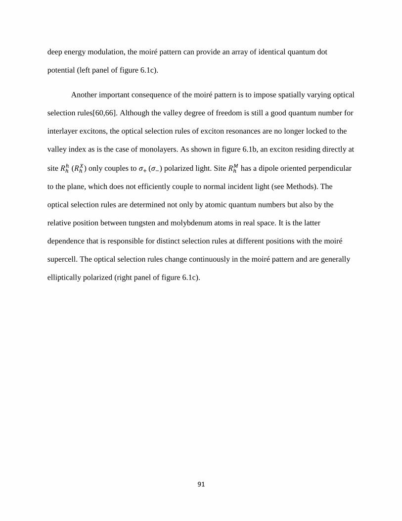
Figure 62 (a) Optical image of an hBN-encapsulated MoSe2WSe2 stacked heterostructure
The hBL region is indicated inside the black dotted line (b) Comparison of the
photoluminescence spectrum from an uncapped heterostructure (dashed curve)
and an hBN-encapsulated heterostructure (solid curve) Neutral (X0) and charged
(X-) exciton emission is observed from the MoSe2 and WSe2 monolayers The
interlayer exciton (IX) emission is observed ~300 meV below the intralayer
resonances (c) Illustrative band diagram showing the type-II alignment and the IX
transition 96
Figure 63 (a) Representative PL spectra shown for hBLs with 1deg and 2deg twist angles Each
spectrum is fit with four (1deg) or five (2deg) Gaussian functions (b) The center
energy of each peak obtained from the fits at different spatial positions across
each sample The average peak spacing increases from 22 plusmn 2 meV to 27 plusmn 3 meV
with twist angle (c) Circularly polarized PL spectrum for + excitation of the 1deg
sample (d) The degree of circular polarization versus emission wavelength
obtained from the spectra in (c) 97
Figure 64 (a) Illustration of the spatial variation of the moireacute potential and the confined multiple IX resonances (b) Optical conductivity of IXs in the K valley in response to (blue line) and (red line) polarized light (c)-(f) Real-space map of the center-of-mass wave functions for peaks (1) (2) (3) and (4) respectively (g)-(h) The spatial variation of the components of the optical matrix elements 101
Figure 65 (a) The three stacking types (
) of the bilayer MoSe2-WSe2
heterostructure and corresponding DFT-calculated band structures (b) Interlayer
distance and the band gap of three stacking types (c) First principles GW-BSE
calculation results for quasiparticle band gap and exciton binding energy for
different stacking types 103
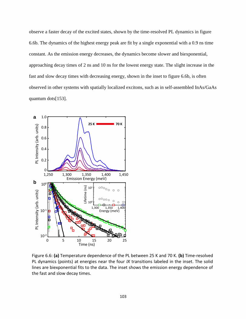
Figure 66 (a) Temperature dependence of the PL between 25 K and 70 K (b) Time-resolved
PL dynamics (points) at energies near the four IX transitions labeled in the inset
The solid lines are biexponential fits to the data The inset shows the emission
energy dependence of the fast and slow decay times 104
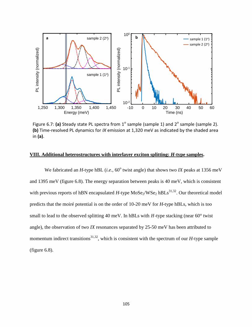
Figure 67 (a) Steady state PL spectra from 1o sample (sample 1) and 2
o sample (sample 2)
(b) Time-resolved PL dynamics for IX emission at 1320 meV as indicated by the
shaded area in (a) 106
xix
Figure 68 Comparison between IX resonances from H-type sample (upper panel) and R-type
sample (lower panel) 107
Figure A1 a) and b) Home-made (thicker film) and commercial PDMS (thinner film) on
microscope slide respectively c) Bulk TMD thinned down on a piece of blue
tape One can tell the quality of the bulk TMD by looking at the flakes Good
quality bulk usually appears with flat cleaved surface In this case the bulk is not
that good but still exfoliatable d) Huge monolayer WSe2 exfoliated on home-
made PDMS 117
Figure A2 a) Schematic of the transfer microscope showing different components b) Actual
picture of the microscope 120
Figure A3 a) 12 PPC liquid inside the glass vial ready to be spin coated b) PMDS dot 122
Figure A4 Watch for contact region during dry transfer process Here the monolayer (on the
PDMS) is at the lower left corner outside the field of view 126
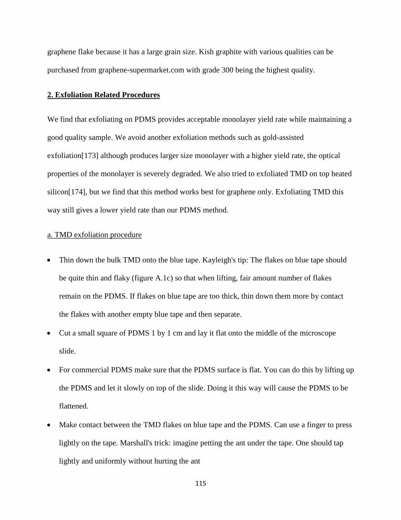
Figure A5 a) PPC transfer steps and b) dry transfer steps for making TMD heterostructure
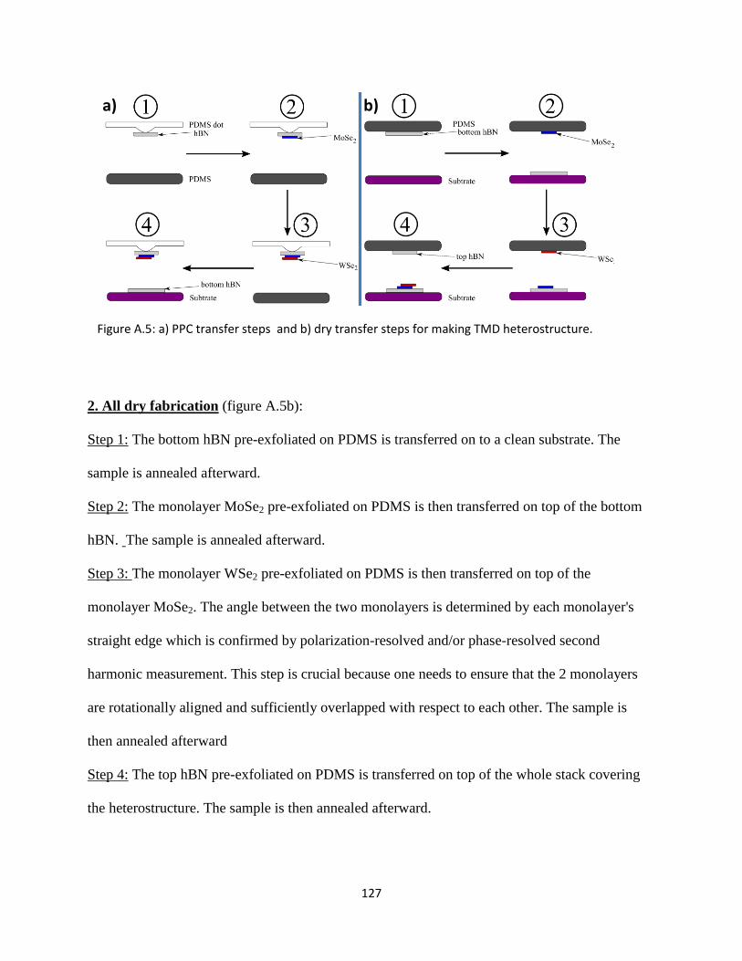
128
Figure A6 PL spectra from monolayer MoSe2 at 10 K excited using 660 nm CW laser with
30 W power The exciton (X) and trion (T) peaks are labeled Keep monolayer
from contact with any chemical during transfer process 130
Figure A7 Temperature chart for annealing TMD sample 131
Figure A8 a) Topography image showing the roughness of monolayer MoSe2 from 2D
semiconductor dry transferred on top of an annealed hBN b) Zoom-in region
from a showing super flat surface c) Lateral force image shows atomic resolution
of the region d) Sample schematic 131
xx
Figure A9 a) and b) Topography image showing the roughness of monolayer MoSe2 from
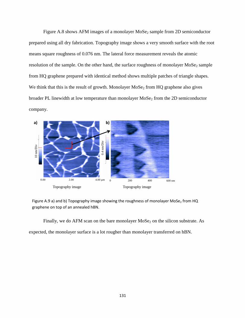
HQ graphene on top of an annealed hBN 132
Figure A10 a) Topography image showing the roughness of monolayer MoSe2 from 2D
semiconductor dry transferred on silicon b) Line cut showing various peaks and
troughs c) Sample schematics 133
1
Chapter 1 Introduction and Overview
One shouldnt work on semiconductor that is a filthy mess who knows if they really exist --
Wolfgang Pauli 1931
The semiconductor is the most significant factor that contributes to the development of the
personal computer cell phone internet camera ie the digital world as we know of today
Semiconductor makes data communication and processing become much faster and electronic
devices much smaller and cheaper than before ie at the time of vacuum tubes Before the advent
of quantum mechanics and band theory experiments on semiconductor were patchily driven by
the needs of technology[1] The purpose of this chapter is to give a brief overview of the
development of semiconductor as well as the introduction of band theory of material This is the
background knowledge in which subsequence chapters are built upon
I Definition of semiconductor
The textbook definition of the semiconductor is the material whose electrical
conductivity is between that of metals and insulators As shown in figure 11 the electrical
conductivity of a semiconductor can vary by three to four orders of magnitude Moreover this
variation can be controlled by various mean ie either by introducing a minute amount of
impurity atoms in the semiconductor or impose an external electric field through electrical
contacts In contrast with metals the electrical conductivity of semiconductor increases as the
temperature increases We can also increase semiconductors electrical conductivity by shining
light with an appropriate wavelength on them - a phenomenon called photoconductivity For a
long time people didnt understand these physical phenomena until the advent of the quantum
theory of solids
2
II Early experiments on semiconductors
Earliest work on semiconductors is by Michael Faraday[16] He found that the electrical
conductivity of silver sulfide increases as a function of temperature - a signature of
semiconductor which is the opposite trend as that of the temperature dependence of metal This
behavior was not understood at the time and was hence labeled as anomalous We now know
that this is due to the exponential increase of charge carriers according to Boltzmann distribution
that more than offset the decrease in mobility due to phonon (lattice vibration) scattering
whereas the near constant number of charges in metal with respect to temperature makes its
electrical conductivity susceptible to phonon scattering[1]
Figure 11 Comparison of electrical conductivities of insulators metals and
semiconductors Figure adapted from ref [1]
3
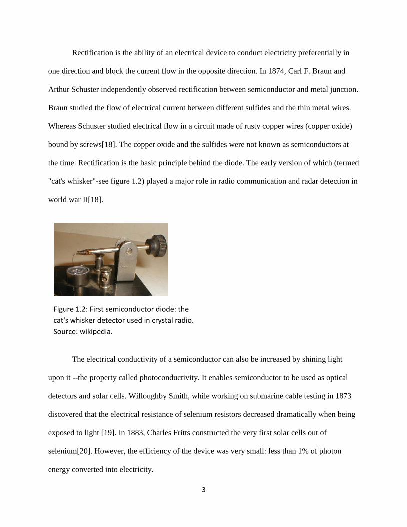
Rectification is the ability of an electrical device to conduct electricity preferentially in
one direction and block the current flow in the opposite direction In 1874 Carl F Braun and
Arthur Schuster independently observed rectification between semiconductor and metal junction
Braun studied the flow of electrical current between different sulfides and the thin metal wires
Whereas Schuster studied electrical flow in a circuit made of rusty copper wires (copper oxide)
bound by screws[18] The copper oxide and the sulfides were not known as semiconductors at
the time Rectification is the basic principle behind the diode The early version of which (termed
cats whisker-see figure 12) played a major role in radio communication and radar detection in
world war II[18]
The electrical conductivity of a semiconductor can also be increased by shining light
upon it --the property called photoconductivity It enables semiconductor to be used as optical
detectors and solar cells Willoughby Smith while working on submarine cable testing in 1873
discovered that the electrical resistance of selenium resistors decreased dramatically when being
exposed to light [19] In 1883 Charles Fritts constructed the very first solar cells out of
selenium[20] However the efficiency of the device was very small less than 1 of photon
energy converted into electricity
Figure 12 First semiconductor diode the
cats whisker detector used in crystal radio
Source wikipedia
4
III From vacuum tube to transistor
The cat whisker detector was difficult to make The material acting as a semiconductor
(usually lead sulfide PbS crystal) often had lots of impurities A good crystal with the favorable
conducting property was hard to be found There was also no way to distinguish between good
versus bad crystal[21] When operating cat whisker required careful adjustment between the
metal wire (whisker) and the semiconducting crystal Moreover this alignment could easily be
knocked out of place[1] Needless to say the cat whisker was cumbersome and was impossible
to mass produced
John Ambrose Fleming invented the vacuum tube in 1904[22] The device consists of
two electrodes inside an airtight-sealed glass tube (Figure 13a) The design of the vacuum tube
evolved from that of the incandescent light bulb The cathode which was often a filament
released electrons into a vacuum when heated -- the process called thermionic emission The
anode which was a metal plate at positive voltage attracted those electrons floating around In
this way the vacuum tube acted as a rectifying device or diode which permits current to flow in
only one direction This current flow can also be controlled if a metal grid is inserted between the
anode and cathode (Figure 13b) By applying the various voltage to the metal grid it was
possible to amplify the current flowing between the anode and cathode This was also the
working principle behind the transistor based on the semiconductor junctions which was later
invented in the 1940s Because of the simple design vacuum tube became a basic component in
electronic devices in the first half of the 20th century The broadcast industry was born[1]
Although vacuum tube performance was better than that of cat whiskers diode electronics
devices made from vacuum tube were bulky and consumed a lot of power After World War II
the proposal was underway to find the replacement for the vacuum tube
5
As mention above point contact detector such as the cats whisker diode performed
poorly due to the bad quality of the semiconductor Thus there was a push for producing high-
quality material particularly silicon and germanium Russel Ohl melts silicon in the quartz tube
and allowed it to cool down slowly 99999 purity silicon was available in 1942[1] In 1947
William Shockley John Bardeen and Walter Brattain successfully demonstrated a working
model of the point contact transistor at Bell Labs made from the high-quality germanium[23]A
few years later Shockley proposed a design for the junction transistor which consisted of 3
layers n-doped layer sandwiched between two p-doped layers[24] In 1950 Shockleys design
was experimentally realized by the work of Gordon Teal Teal made the p-n-p junction transistor
Figure 13 a) Schematic of the vacuum tube that only permits electricity to flow in one
direction Electrons can flow from hot cathode to anode but not the other way around b)
Metal grid inserted in the space between the anode and cathode can control the current
flow between anode and cathode Source wikipedia
a) b)
6
from high purity germanium he grew in the lab[25] From there the transistor was ready to be
mass produced and gradually replaced the use of vacuum tubes in everyday electronics
IV Some concepts and ideas of band theory
Much of the development of semiconductor technology in the early 20th century owed to
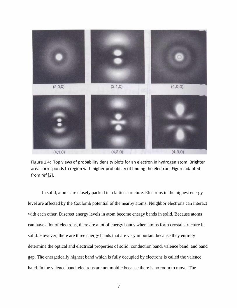
the success of band theory - a manifestation of quantum mechanics in a solid state system In
quantum mechanics an electron can be mathematically described by its wave-function which is
often a complex number function of the position and time The magnitude squared of the wave-
function gives the probability density of the electron ie the probability to find the electron at a
given moment in time in a particular unit volume of space In this framework the electron
behaves like a wave So if its being confined (by some energy potential) its wave-function and
energy will be quantized very much like the guitar string being held fixed on both ends The
situation can be generalized for electron confined in hydrogen atom by the electrostatic Coulomb
potential The probability densities of this electron as functions of the position for different
energy levels[2] are depicted in figure 14
7
In solid atoms are closely packed in a lattice structure Electrons in the highest energy
level are affected by the Coulomb potential of the nearby atoms Neighbor electrons can interact
with each other Discreet energy levels in atom become energy bands in solid Because atoms
can have a lot of electrons there are a lot of energy bands when atoms form crystal structure in
solid However there are three energy bands that are very important because they entirely
determine the optical and electrical properties of solid conduction band valence band and band
gap The energetically highest band which is fully occupied by electrons is called the valence
band In the valence band electrons are not mobile because there is no room to move The
Figure 14 Top views of probability density plots for an electron in hydrogen atom Brighter
area corresponds to region with higher probability of finding the electron Figure adapted
from ref [2]
8
conduction band is the next higher energy band which is generally empty Electrons in the
conduction band are free to move and are not bound to the nucleus The energy difference
between the valence band and the conduction band is called the band gap The size of the band
gap (in electron-volt unit) determines whether the material is conductor semiconductor or
insulator (figure 15)
In solid state physics one usually encounters two types of energy band plots band
diagram and band structure Band diagram is the plot showing electron energy levels as a
function of some spatial dimension Band diagram helps to visualize energy level change in
hetero-junction and band bending Band structure on the other hand describes the energy as a
function of the electron wavevector k - which is also called the crystal momentum
Semiconductors fall into two different classes direct and indirect bandgap In direct (indirect)
gap semiconductors conduction band minimum occurs at the same (different) point in k-space as
the valence band maximum as illustrated in the band diagram figure 16 Since a photon or light
has negligible momentum compared to an electron ( ) the process
Figure 15 Energy band gaps for (a) metal -- zero energy gap (b) semiconductor -- 1 to 2 eV
gap (c) insulator -- larger than 3 eV gap
9
of absorbing or emitting a photon can only promote or induce an electron to undergo a vertical
(with nearly zero momentum change) transition in the dispersion curve An electron (hole)
electrically injected or optically promoted to the conduction quickly relaxes to the bottom (top)
of the conduction (valence) band Consequently optical absorption or emission processes are
much more efficient in direct-gap semiconductors than those in the indirect gap semiconductors
Well-known examples of direct (indirect) gap semiconductors are GaAs and GaN (Si and
Ge)[26]
Figure 16 In a direct (indirect) bandgap material the CB minimum and the VB
maximum occur at the same (different) position in momentum space as illustrated
in panel a ( panel b)
gEgE
k k
0 0
a) b)
10
Chapter 2 Introduction to monolayer transition metal dichalcogenides
(TMDs)
Two dimensional (2D) materials consist of a single layer of element or compound
Interest in 2D material started since the isolation and characterization of graphene in 2004 Since
then tens of thousands of papers on graphene has been published[27] In 2010 Nobel prize in
physics was awarded for Geim and Novoselov for groundbreaking experiments regarding the
two-dimensional graphene[28] Graphene itself is an excellent electrical conductor[29]
However its lack of band gap has limited its applications in electronic and optoelectronic
devices Over the years new types of 2D materials with diverged properties have emerged such
as the ferromagnetic Cr2Ge2Te6[30] CrI3[15] superconductive such as 1T-SnSe2[717]
insulating such as hBN[31]
Transition metal dichalcogenides (TMDs) are members of 2D materials family and are
semiconductors with a band gap in the visible range of the electromagnetic spectrum Two
studies in 2010 simultaneously reported these new 2D semiconductors [332] Their properties
are especially interesting including an evolution from indirect in bulk material to direct bandgap
in monolayer[332] tightly bound excitons (coulomb bound electron-hole pairs) due to two-
dimensional effect [533] large absorption per monolayer (~10) [34] and spin-valley coupling
[1235-37] This chapter will briefly survey the physics behind some of these interesting
properties of monolayer TMD
I TMD lattice structure and polymorphs
Transition metal dichalcogenide (TMD) has the chemical formula of MX2 where M
stands for a transition metal and X stands for a chalcogen The atomic structure of bulk TMD
11
consists of many layers weakly held together by van der Waal (vdW) forces[14] Within each
monolayer the metal layer is sandwiched between two chalcogen layers and is covalently
bonded with the chalcogen atoms ie strong in-plane bonding[4] as shown in figure 21 It is the
former that allows TMD to be easily mechanically exfoliated into thin layer forms monolayer
bilayer trilayer etc
Monolayer TMDs mainly have two polymorphs trigonal prismatic (2H) and octahedral
(1T) phases The difference in these structures is how the chalcogen atom layers arranged around
the metal layer In the 2H(1T) phase chalcogen atoms in different atomic planes are located right
on top of (a different position from) each other in the direction perpendicular to the monolayer
(side view in fig II1) Either 2H or 1T can be thermodynamically stable depending on the
particular combination of transition metal (group IV V VI VII IX or X) and chalcogen (S Se
or Te) For example MoS2 MoSe2 WS2 WSe2 form 2H phase[38] These materials are the
main focus of our study In contrast WTe2 thermodynamically stable phase is 1T at room
temperature[39]
12
II Evolution from indirect bandgap in bulk material to direct bandgap in
monolayer
Most TMDs (eg MoS2 MoSe2 WSe2) are found to exhibit an indirect to direct gap
transition as the layer thickness is reduced to a monolayer leading to the drastic increase in
photon emission efficiency[332] Monolayer TMDs reciprocal lattice is a hexagon with the
center of Brillouin zone denoted as the gamma point G and the vertices at the K points (see
figure 22a) In the bulk material the maximum of the valence band is at G point whereas the
minimum of the conduction band is at the Q point - between G and K point (see figure 22b left
panel) The conduction band states and the valence band states near K point are mainly
composed of strongly localized orbitals at the Mo atoms (valence band) and
states (conduction band) slightly mixed with the chalcogen orbitals They have minimal
Figure 21 Two main structure polymorphs of TMD 2H trigonal prismatic and 1T
octahedral The crimson (gray) circle represents chalcogen(metal) atom The red (gray)
shadow represents primitive (computational) cell Figure adapted from ref [4]
Top
vie
wSi
de
vie
w
13
interlayer coupling since Mo atoms are sandwiched between two layers of S atoms[32] On the
other hand conduction at the Q point and valence band at G point originate from the linear
combination of anti-bonding pz orbital of S atoms and d orbitals of Mo atoms They have strong
interlayer coupling and their energies depend on layer thickness As layer thickness reduces the
indirect gap becomes larger while the direct gap at K point barely changes By tracking the shift
the photoluminescence (PL) peak position with layer number in MoS2 it has been shown that
indirect gap shifts upwards in energy by more than 06 eV leading to a crossover from an
indirect gap in bulk to direct gap in monolayer[3] As a consequence monolayer TMD is much
brighter than the bilayer TMD shown in figure 22c
III Excitons
Excitons (X) are electron-hole pairs bound together by Coulomb force ie an electron in
the conduction band binding with a hole in the valence band (figure 23c) Classically in the real
Figure 22 a) The Brillouin zone of monolayer TMD showing the path in which the band
structure is drawn in part b b) Calculated band structure of bulk and 1 layer MoS2 The
solid arrows indicate the lowest energy transitions Bulk (1 layer) has indirect (direct)
bandgap c) PL measurement with different layers 1 layer MoS2 has much higher
luminescence than 2 layer MoS2 Figure adapted from ref [3]
G M
K
a) b) c)
Bulk Monolayer
Q
Q
Q
14
space representation exciton can be thought of as negative electron and positive hole orbiting
around each other (figure 23a) and freely move to abound in the crystal In fact the quantum
mechanics picture of the exciton is slightly more complicated We take a look at the wave
function of the ground state exciton in a crystal The concept of correlated electron-hole motion
is illustrated in figure 23b in which the position of the hole is assumed to be at the origin
indicated by the black circle The electron wave function is spanning over many lattice sites
Quantitatively we can model the exciton similarly to a hydrogen atom using the effective
electron(e) mass and effective hole(h) mass[26] We can also separate the X wave-function into
two parts the relative motion between e and h and the center of mass motion The center of
mass motion behaves like a free particle with the reduced mass m of e and h given by
whereas the relative motion results in hydrogen-like energy level We note the basic equation
describing the energy of an exciton here which has contributions from both relative and center
of mass motion
The first term is the band gap of the semiconductor The second term is the primary
correction to the band gap and causes the X energy to be lower than the band gap energy by the
amount EB which is the X binding energy which is often written as
where aB is the
exciton Bohr radius Often the exciton Bohr radius is used as a measure of how large the exciton
is In monolayer TMD the exciton binding energy is huge because of the reduced
dimensionality Therefore the exciton Bohr radius in monolayer TMD is small about few
nanometers compared to tens of nanometers exciton in the traditional quantum well[26]
15
Formally exciton in monolayer TMD can be thought of as Wannier-Mott exciton whose
mathematical description is shown in the preceding equation
The third term of the energy equation gives rise to the parabolic form of the exciton
dispersion curve - see figure 23c corresponding to the kinetic energy arise from the free motion
of the center of mass When the exciton energy level n is large only the energy band gap Eg and
the kinetic energy term dominate Indeed a series of exciton excited states can often be observed
in the absorption spectrum from a multilayer MoS2 with gradually decreasing oscillator strength
for higher excited states[14] as shown in figure 23d In monolayer TMD the absorption of the
exciton higher excited states (ngt2) are very weak - barely visible in the absorption spectrum One
often needs to take the derivative of the reflectance contrast[5] - see figure 23e
16
Exciton in monolayer TMD is very robust due to strong binding energy between electron
and hole which is in the order of a few hundred mili-electronvolts making it stable at room
temperature These excitons have such strong binding energy is due to the reduced dielectric
screening in two-dimensional system The electric field lines between electron and hole extend
outside the sample plane in monolayer as shown in figure 24a bottom panel The electron and
hole are being pulled closer together giving rise to smaller exciton Bohr radius On the other
Figure 23 a) Schematic of real space representation of an exciton b) The modulus squared
of the electron wave function of an exciton in which the hole position is fixed at the center
black circle The inset shows the corresponding wave function in momentum space across
the Brillouin zone Figure adapted from ref [6] c) Representation of the exciton in reciprocal
space d) Dispersion curve for the exciton with different excited states in a direct band gap
semiconductor with energy gap Eg and exciton bind energy EB labeled e) Exciton series
measured in the absorption spectrum of a multi-layer MoS2 Figure adapted from ref [14] f)
Derivative of the reflectance contrast spectrum of a monolayer WS2 showing the emergence
of higher excited exciton states Figure adapted from ref [5]
gE
k
0
1Bn
2Bn
3Bn
Bn
BE
2035 2010 1985 1960
5
75
10
Energy (meV)
Per
cen
tage
Tra
nsm
issi
on
1s
2s3s
4s5s
d) e) f)
a) b) c)
17
hand the Coulomb interaction in the 3D system is screened out by the surrounding bulk material
effectively weaken the binding energy between electron and hole The distance between electron
and hole is also further than the 2D case (figure 24a top panel)
To measure the exciton binding energy experimentally one must identify the absolute
energy positions of both exciton resonance EX and free particle band gap Eg The binding energy
is then easily calculated by the relation EX can be measured by the optical
method such as absorption shown in figure 23f Here EX corresponds to the energy position of
the 1s state On the other hand Eg cannot be determined by the optical measurement which is
strongly influenced by excitonic effects A direct approach is to use scanning tunneling
spectroscopy (STS) technique which measures tunneling currents as a function of the bias
voltage through a tip positioned very close to the sample STS can probe the electron density of
states in the vicinity of the band gap revealing the energy levels of free electrons in the valence
band and the conduction band A typical STS spectrum for monolayer MoSe2 on bilayer
graphene is shown in figure 24c The band gap is the difference between onsets which is 216
eV for monolayer MoSe2
18
Figure 24 a) Schematic represents exciton in 3D (bulk) and 2D (monolayer) TMD b) The
effect of increased binding energy in 2D system due to reduced dielectric screening The
binding energy is indicated by the dash red double arrows Figure adapted from ref [5] c)
Logarithm of a typical dIdV curve obtained from scanning tunneling microscopy
measurement of monolayer MoSe2 used to obtain band gap value Figure adapted from ref
[15]
Bulk 3D
Monolayer 2D
Log
(dI
dV
) (d
ecad
ed
iv)
-35 -30 -25 -20 -15 -10 -05 00 05 10 15
Bias Voltage (Volts)
(c)
19
IV K-K valleys in monolayer TMD
Valley refers to the energy extrema in the band structure (energy minima in the
conduction band and energy maxima in the valence band) As mention in the previous chapter
the reciprocal lattice of a monolayer TMD is a hexagon with three-fold rotational symmetry
corresponding to three-fold symmetry of the real lattice Although the Brillouin zone of a
monolayer has 6 vertices only two of the K and K are inequivalent because other vertices can be
mapped back to either K or K by either b1 or b2 - the reciprocal lattice vector The direct band
gap of the monolayer TMD occurs at the K and Krsquo valley The exciton at K and K valley only
interact with σ+ and σ- circularly polarized light respectively due to chiral optical selection rules
which can be understood from group theory symmetry argument The orbital Bloch functions of
the valence band states at K K points are invariants while the conduction band states transform
like the states with angular momentum components plusmn1 inherited from the irreducible
representations of the C3h point group[3540] Therefore the optical selection rules of the
interband transition at KK valley can only couple to σplusmn light respectively as illustrated in figure
25b
20
V Dark excitons
As we discussed in the previous section exciton can be modeled as the hydrogen atom in
which the negative electron orbits the positive hole This gives rise to different excited state 1s
2s 3s (see figure 23) Among them the 1s exciton state dominates the optical properties of
the monolayer TMD By definition bright(dark) exciton can(cannot) interact (absorbemit) with
photon As a result bright exciton has a much shorter lifetime than dark exciton because electron
and hole in bright exciton can recombine and emit a photon There are many reasons that make
an exciton dark
1 Spin forbidden dark exciton
Spin forbidden dark exciton consists of the anti-parallel spin conduction band and
valence band as illustrated in figure 26a Here the arrow next to the band indicates the direction
of electron spin To be able to interact with a photon the total spin of electrons forming an
Figure 25 a) The Brillouin zone of monolayer TMD with the reciprocal lattice vectors b1
b2 b) Band structure of monolayer WSe2 around K and Krsquo points Exciton at K and Krsquo
valley couples to light with σ+ and σ- polarization respectively
a)
K
K
K
Krsquo
KrsquoKrsquo
ky
kx
b1
b2
K Krsquo
_
+
σ+
_
+
σ-
b)
21
exciton must add up to 1 This is the familiar conservation of angular momentum in which the
spin-forbidden dark exciton is not satisfied
The order and energy difference between bright and dark exciton is given by the sign and
amplitude of the spin splitting in the conduction band[741] As a result for the tungsten-based
monolayer TMD such as WS2 and WSe2 the bright exciton is the second lowest energy 1s
exciton (left side of figure 26a) Whereas in molybdenum case the bright exciton is the lowest
energy exciton (right side of figure 26a) This difference is one of the reasons leading to the
contrasting behavior of exciton luminescence with respect to temperature For example
monolayer WX2(MoX2) is brighter(dimmer) as the temperature increases Also monolayer WX2
exciton has more robust valley polarization and valley coherence in steady-state PL than that of
monolayer MoX2 These differences are thought to be the result of the interplay between the
spin-forbidden dark exciton momentum indirect dark exciton and phonon which is discussed in
great details in ref [41]
There are several experimental techniques to measure the energy splitting between the
bright and spin forbidden dark exciton Strong in-plane magnetic field (~30T) mixes the bright
exciton and the dark exciton states which allow for the detection of dark transitions that gain
oscillation strength as the magnetic field increases[3142] Another method is to take advantage
of the emission polarization of the dark exciton Symmetry analysis shows that the spin-
forbidden dark exciton is not completely dark It couples to light whose polarization in the z-axis
(normal to the plane of the monolayer) In fact if the monolayer is excited and collected from the
edge of the monolayer strong peak 40 meV below the neutral exciton peak emerges in the PL
spectrum of monolayer WSe2[43] corresponding to the conduction band splitting High NA
objective also gives rise to the out of plane optical excitation polarization As a result the spin
22
forbidden dark exciton also shows up in normal incidence PL when high NA (numerical
aperture) objective is used[43]
Figure 26 Different types of dark excitons a) Spin forbidden dark exciton in
tungsten(molybdenum) based monolayer TMD denoted WX2 and MoX2 respectively b)
Momentum indirect dark exciton in which electron and hole are not in the same valley
c) Momentum indirect dark exciton in which same valley electron located outside of the
light cone Figures adapted from ref [7]
K Krsquo
_
+
a)
b)
brightdark
K Krsquo
+
_
brightdark
c)
WX2 MoX2
23
2 Momentum indirect dark exciton
Momentum indirect dark exciton composes of parallel spin electrons but located at
separate valleys in the band structure (figure 26b) or the electron located outside of the light
cone (figure 26c) In order to interact with light the momentum indirect exciton needs to
exchange momentum with phonon to make up for the momentum difference Higher temperature
gives rise to more phonons Thus one would expect the indirect momentum exciton gets brighter
with respect to increased temperature
VI Valley property of excitonic states (ie exciton trion)
1 Valley polarization
Valley polarization often refers to the population difference between K and K valley
Based on the spin-valley locking one can selectively excite carriers with the excitation energy
above the band gap in K (K) valley using σ+ (σ-) circular polarized light Electrons and holes
then relax to the band edge to form excitons which can be radiatively recombined to emit
photons The degree of valley polarization for an excitonic state (exciton trion) in PL signal is
usually quantified by the formula
Where Ico_circ (Icross_circ) is the PL signal that emits at the same(opposite) circular polarization with
the excitation polarization By writing out the rate equation explicitly taking into account the
population generated by optical pumping population recombination and relaxation it can be
shown that[12]
24
Where τA and τAS are the total lifetimes and the intervalley relaxation time of the exciton Thus
if it takes longer or comparable time for the exciton to scatter across the valley (intervalley
scattering) than the exciton total lifetime the circularly polarized emission from exciton will be
observed Figure 27ab shows the circular polarized steady-state PL for monolayer MoS2 and
monolayer WSe2 respectively On the other hand the valley relaxation time of the exciton in
monolayer WSe2 at cryogenic temperature has been measured by the circular pump probe
technique to be less than 1ps[44] The total lifetime of the WSe2 monolayer exciton is even faster
~200 fs[45] Remarkably the spin lifetime of the free carrier electron and hole in monolayer
TMD is extremely long on the order of a few nanoseconds[46] The primary cause of the fast
depolarization of the exciton is the intervalley electron-hole exchange interaction [11] which can
quickly annihilate bright exciton in K valley accompanying with the creation of bright exciton in
opposite valley K[47]
25
2 Valley coherence
Valley coherence refers to the phase preservation (coherence) between K and K valley
exciton One can readily observe the valley coherence of exciton in monolayer TMD by
excitation using linear polarized light and measuring the linear polarized PL signal Linearly
polarized light can be considered as a superposition of σ+ and σ- polarization Thus if the linear
polarization of the emitted light from the exciton is preserved so is the coherence between K and
Figure 27 a) The circular polarized photoluminescence spectrum of monolayer MoS2 at
14K The excitation energy is indicated by the arrow which is 196 eV Figure adapted
from ref [12] b) The circular polarized photoluminescence spectrum of monolayer WSe2
at 4K excited with the same energy as part a) Figure adapted from ref [11] X0 and X-
denote the exciton and trion peak respectively
co circular
cross circular
17 18 19 20 21 22 23
1800
1500
1200
900
600
300
0
PL
inte
nsi
ty (
au
)
Photon energy (eV)
co circular
cross circular
160 165 170 175
Photon energy (eV)
PL
inte
nsi
ty (
au
)
120
240
360
a)
b)
0
X0
X0X-
26
K valley excitons Following the definition of the degree of valley polarization we can define
the degree of valley coherence as
Where Ico_lin (Icross_lin) is the PL signal that emits at the same(orthogonal) linear polarization with
the excitation polarization By pumping above the exciton resonance the valley coherence of the
exciton in monolayer TMD has readily observed if the excitation energy is close to that of the
exciton Figure 28a shows the linear polarized PL signal on monolayer WSe2 pumping at 188
eV[11] Figure 28b shows that the intensity of the neutral exciton is maximized whenever the
detection polarization is in the same polarization of the excitation
27
Figure 28 a) The linear polarized PL of monolayer WSe2 at cryogenic temperature
excited with 188 eV CW laser Different gate voltages are used to control the
emergence of neutral exciton X0 negative trion X- and positive trion Co(cross) linear
detection is plotted as the black(red) curves b) Normalized neutral exciton intensity
peak as a function of detection polarization angles Figures adapted from ref [11]
28
VII Trions
1 Definition and basic properties
Trion or charged exciton is the exciton bound with an extra electron ie negative trion or
an extra hole ie positive trion The binding energy of trion is defined as the energy difference
between exciton peak and trion peak either in PL or absorption measurement Trion binding
energy in monolayer TMD is about 20 to 40 meV which is one order of magnitude stronger than
trion in GaAs quantum well[848] The samples fabricated by CVD or mechanical exfoliation are
often n-type (negatively doped with extra electrons) The formation of trions is very
likely[4950] Strong trion binding energy is also due to reduced dielectric screening discussed in
the previous section In contrast to exciton trion is a charged particle Therefore it directly
influences electrical transport in a semiconductor The process of the exciton capturing an extra
charge to form trion is energetically favorable Indeed by using the pump probe technique we
have directly measured this process to be happening in a few pico-second timescales[51]
In fact one can adjust the doping level in the sample by fabricating metal contacts in
order to control the emergence of negative or positive trions One such example is shown in
figure 25a where a monolayer MoSe2 is put under two metal contacts The gate voltage is then
varied to p-dope the sample with extra holes (negative gate voltage) or n-dope the sample with
extra electrons (positive gate voltage) The PL spectrum of the monolayer is monitored as a
function of the gate voltage in figure 29c Four prominent features can be seen in figure 29c At
Vg=0 exciton sharp peak shows up at 1647 eV and impurity broad peak is at 157 eV Trion
shows up at either negative or positive gate voltage at energy 1627 eV Thus the trion binding
energy in monolayer MoSe2 is 20 meV The similarity in energy between positive and negative
29
trions indicates that the electron and the hole in monolayer TMD have approximately the same
effective mass which is consistent with the theoretical calculations [3052] More interestingly
n-dope regime gives rise to two types of trions intervalley and intravalley trion which show up
in the absorption spectrum of the monolayer if the linewidth is sufficiently narrow (figure 25d)
These two types of trions will be discussed in the next subsection
30
Figure 29 a) Microscopic image of a monolayer MoSe2 and the two metal contact b) Device
schematic to control the doping level in the sample c) PL spectrum of the monolayer as a
function of gate voltage The labels are as followed X0 exciton X- negative trion X+ positive
trion XI impurity peak Figures adapted from ref [8] d) Contour plot of the first derivative of
the differential reflectivity in a charge tunable WSe2 monolayer Double trion peaks emerge
at the n-dope regime Figure adapted from ref [17]
Vg
Ene
rgy
(eV
) PL
inte
nsi
ty (
au
)
Exciton
Trion
a)
b)
c)
d)
31
2 Intervalley and intravalley trion in monolayer TMD
Trion is a charged exciton - exciton bound to an extra hole or extra electron If the extra
electron or hole resides in the same(opposite) valley as the excited electron-hole pair the trion is
called intravalley(intervalley) trion Because the exfoliated monolayer TMD on a substrate is
unintentionally n-doped[4453] we will restrict our discussion to the negative trions only The
charge configurations of different species of trion are shown in figure 210
The conduction band splitting has a different sign for W-based monolayer and Mo-based
monolayer Because bright exciton is not the lowest energy exciton in monolayer WSe2 an extra
electron from either the same valley or from opposite valley can bind with the exciton to form
trion (figure 210a and b) On the other hand bright exciton in monolayer MoSe2 is the lowest
energy exciton so extra electron must come from the opposite valley to form trion Intravalley
trion in monolayer MoSe2 is much higher in energy than intervalley trion (figure 210c) and is
energetically unfavorable to form
Figure 210 Charge configuration of (a) intravalley trion (b) intervalley trion of
monolayer WSe2 and (c) intervalley trion of monolayer MoSe2
a) b) c)
Monolayer WSe2 Monolayer MoSe2
Intravalley trion Intervalley trion Intervalley trion
32
Inter- and intravalley trion in hBN encapsulated monolayer WSe2 has been observed
experimentally in PL signal at cryogenic temperature[54] The energy splitting between
intervalley and intravalley trion due to electron-hole interaction is predicted and observed to be 6
meV It turns out that because of the charge configuration intravalley trion can retain its valley
polarization about two orders of magnitude longer than intervalley trion This is one of our own
contributions to the field and will be discussed in more details in the later chapter
33
Chapter 3 Introduction to TMD heterostructure
In this chapter well look at the properties of TMD heterostructure particularly TMD
vertical heterobilayer (hBL) which possesses type II band alignment[55-57] and can host
interlayer exciton (IX)ndash with electron and hole localized in different layers Interlayer exciton
has a much weaker dipole moment about two orders of magnitude[58] and much longer lifetime
three order of magnitude than the intralayer exciton counterpart[13] Moreover heterobilayer
composed of monolayers with a slightly different lattice constant andor twist angle can give rise
to Moireacute superlattice[5960] with unique effects on the interlayer exciton potential landscape and
optical properties[61]
I TMD heterobilayer band alignment and optical properties
TMD vertical heterobilayer is made of two monolayers stacked on top of one another
either by transfer of mechanically exfoliated monolayer or CVD (chemical vapor deposition)
growth Due to different band gap and the work function of two constituent monolayers TMD
heterostructure has type II band alignment where the conduction band minimum is in one layer
and the valence band maximum is in other[55] Several experiments have measured the band
alignment directly in TMD heterobilayers Sub-micrometer angle-resolved photoemission
spectroscopy determines the valence band offset of MoSe2-WSe2 heterobilayer to be 300 meV
with the valence band maximum located at K and K points[62] Type II band alignment is also
found by scanning tunneling microscopy measurement on MoS2-WSe2 heterobilayer with
valence band (conduction band) offset of 083 eV (076 eV) at K and K points[57] Thus
electrons and holes once created quickly transfer and accumulate in the opposite layers in few
tens of femtoseconds timescale[63] Electron and hole residing in different layers bind together
34
by Coulomb attraction forming interlayer exciton (IX) Early experiment on MoSe2-WSe2
heterobilayer has reported the observation of interlayer exciton PL signal at the cryogenic
temperature around 14 eV(figure 31c) The spatial separation of electron and hole results in
much weaker dipole moment (around two orders of magnitude) of interlayer exciton than that of
the intralayer counterpart Thus as a consequence the interlayer exciton lifetime is much longer
in order of nanoseconds compared to just a few picoseconds of intralayer exciton[6465] at
cryogenic temperature
35
Valley physics of interlayer exciton is especially interesting In the simplest case with
zero twist angle the conduction band K (K) valley from MoSe2 is aligned with valence band K
(K) valley from WSe2 in momentum space (figure 31b) The interlayer exciton is thus a
momentum direct exciton As the twist angle increase the conduction band minimum moves
away from the valence band maximum at K point[66] The IX becomes indirect in momentum
space with decreasing dipole moment decreasing emission intensity and longer
lifetime[106167] At 60o Krsquo conduction band minimum is aligned with the K point valence
Figure 31 a) Type II band alignment of MoSe2-WSe2 heterobilayer The conduction band
minimum (valence band maximum) is belong to monolayer MoSe2(WSe2) Charge transfer
intra- and interlayer exciton recombination timescales are indicated b) Band structure of
the aligned TMD heterostructure at 0 degree stacking angle Conduction band K(K) valley
from MoSe2 is aligned with valence band K(K) valley from WSe2 in momentum space c)
The low temperature PL spectrum of an aligned heterobilayer MoSe2-WSe2 featuring
interlayer exciton (IX) peak around 14 eV Figure adapted from ref [13]
WSe2
MoSe2- -
-
+++
IX
~10 fs
~10 fs
~1 ps ~1 ps~10 ns
K Krsquo
_
+
K Krsquo
0o stacking
IX
13 14 15 16 17 18
Energy (eV)
Inte
nsity (
au
)a) b)
c)IX
36
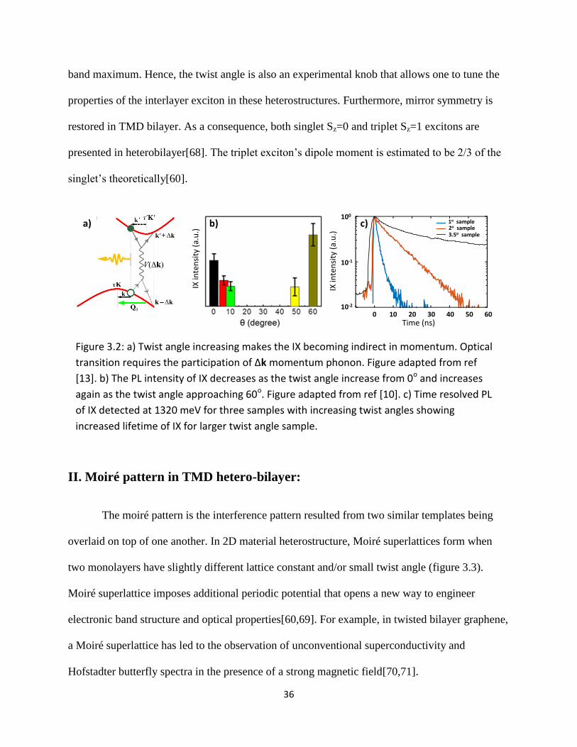
band maximum Hence the twist angle is also an experimental knob that allows one to tune the
properties of the interlayer exciton in these heterostructures Furthermore mirror symmetry is
restored in TMD bilayer As a consequence both singlet Sz=0 and triplet Sz=1 excitons are
presented in heterobilayer[68] The triplet excitonrsquos dipole moment is estimated to be 23 of the
singletrsquos theoretically[60]
II Moireacute pattern in TMD hetero-bilayer
The moireacute pattern is the interference pattern resulted from two similar templates being
overlaid on top of one another In 2D material heterostructure Moireacute superlattices form when
two monolayers have slightly different lattice constant andor small twist angle (figure 33)
Moireacute superlattice imposes additional periodic potential that opens a new way to engineer
electronic band structure and optical properties[6069] For example in twisted bilayer graphene
a Moireacute superlattice has led to the observation of unconventional superconductivity and
Hofstadter butterfly spectra in the presence of a strong magnetic field[7071]
Figure 32 a) Twist angle increasing makes the IX becoming indirect in momentum Optical
transition requires the participation of Δk momentum phonon Figure adapted from ref
[13] b) The PL intensity of IX decreases as the twist angle increase from 0o and increases
again as the twist angle approaching 60o Figure adapted from ref [10] c) Time resolved PL
of IX detected at 1320 meV for three samples with increasing twist angles showing
increased lifetime of IX for larger twist angle sample
IX in
ten
sity
(a
u)
IX in
ten
sity
(a
u)
100
10-1
10-2
0 10 20 30 40 50 60Time (ns)
2o sample1o sample
35o sample
a) b) c)
37
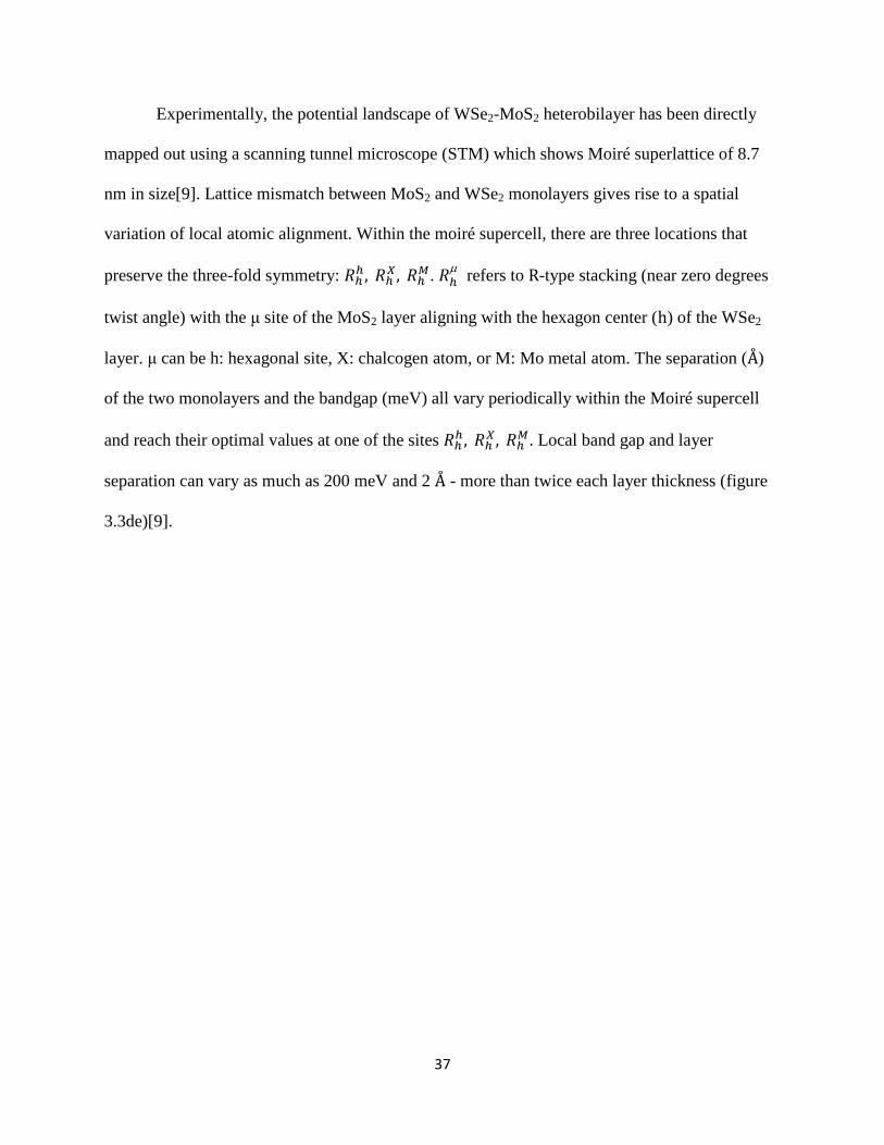
Experimentally the potential landscape of WSe2-MoS2 heterobilayer has been directly
mapped out using a scanning tunnel microscope (STM) which shows Moireacute superlattice of 87
nm in size[9] Lattice mismatch between MoS2 and WSe2 monolayers gives rise to a spatial
variation of local atomic alignment Within the moireacute supercell there are three locations that
preserve the three-fold symmetry
refers to -type stacking (near zero degrees
twist angle) with the site of the MoS2 layer aligning with the hexagon center ( ) of the WSe2
layer can be h hexagonal site X chalcogen atom or M Mo metal atom The separation (Å)
of the two monolayers and the bandgap (meV) all vary periodically within the Moireacute supercell
and reach their optimal values at one of the sites
Local band gap and layer
separation can vary as much as 200 meV and 2 Å - more than twice each layer thickness (figure
33de)[9]
38
Figure 33 a) STM image of rotational aligned WSe2-MoS2 heterobilayer showing the moireacute
superlattice period of 87 nm b) Moireacute supercell with
denoting the locations
that retain the three fold symmetry c) Zoom in view showing the specific atomic
alignment d) and e) Layer separation and band gap variation of the TMD moireacute pattern
respectively Figures adapted from ref [9]
25
20
15
10
05
000 5 10 15 20 25
Hei
ght
(Å)
Spatial dimension (nm)14
12
10
08
06
04
Ban
d g
ap (
eV
)
a)
b)
c) d)
e)
39
Chapter 4 Experimental Techniques
In this chapter we describe in details the working principle as well as the makeup
components of various optical techniques in the lab These include linear optical measurements
such as photoluminescence and white light absorption as well as nonlinear techniques such as
pump-probe spectroscopy and second harmonic generation
I Photoluminescence (PL)
PL measurement is one of the most widely used optical techniques for the
characterization of semiconductors PL is light emitted when photo-excited carriers decay from
the higher excited state to lower excited or ground state[72] These emission states may be defect
levels continuum levels in the conduction or valence bands or exciton states Thus the
interpretation of PL spectrum requires detailed knowledge of the energy levels of the sample
However PL measurement is a very quick simple and powerful characterization tool For
example the PL of the TMD sample at room temperature helps identify whether the sample is
monolayer or bilayer This is our method to verifyensure monolayer sample Exciton PL
linewidth of monolayer TMD sample at cryogenic temperature tells us about samples quality
Higher quality sample with low defect density gives rise to lower inhomogeneous broadening
and narrower linewidth[73] Other advantages of PL measurement include its ability to indirectly
measure the non-radiative recombination rate its ability to investigate very shallow levels and
yield information about the symmetry of an energy level[72] PL is also non-destructive requires
only a very small amount of material to work with PL can also be readily combined with other
tools to yield greater information about the material such as external magnetic field external
40
electric field and electrical doping (by means of metal contacts) pressure (by incorporating
pressure cell) temperature (cryostat)
Photoluminescence excitation (PLE) spectroscopy is a variation of PL measurement in
which the excitation energy is tuned through a particular energy level in order to excite
luminescence transitions related to the level being pumped PLE is an important tool for
investigating relationships between different luminescence transitions For example in this
report[74] PLE has been used to establish the moireacute exciton as the origin of multiple intralayer
exciton peaks
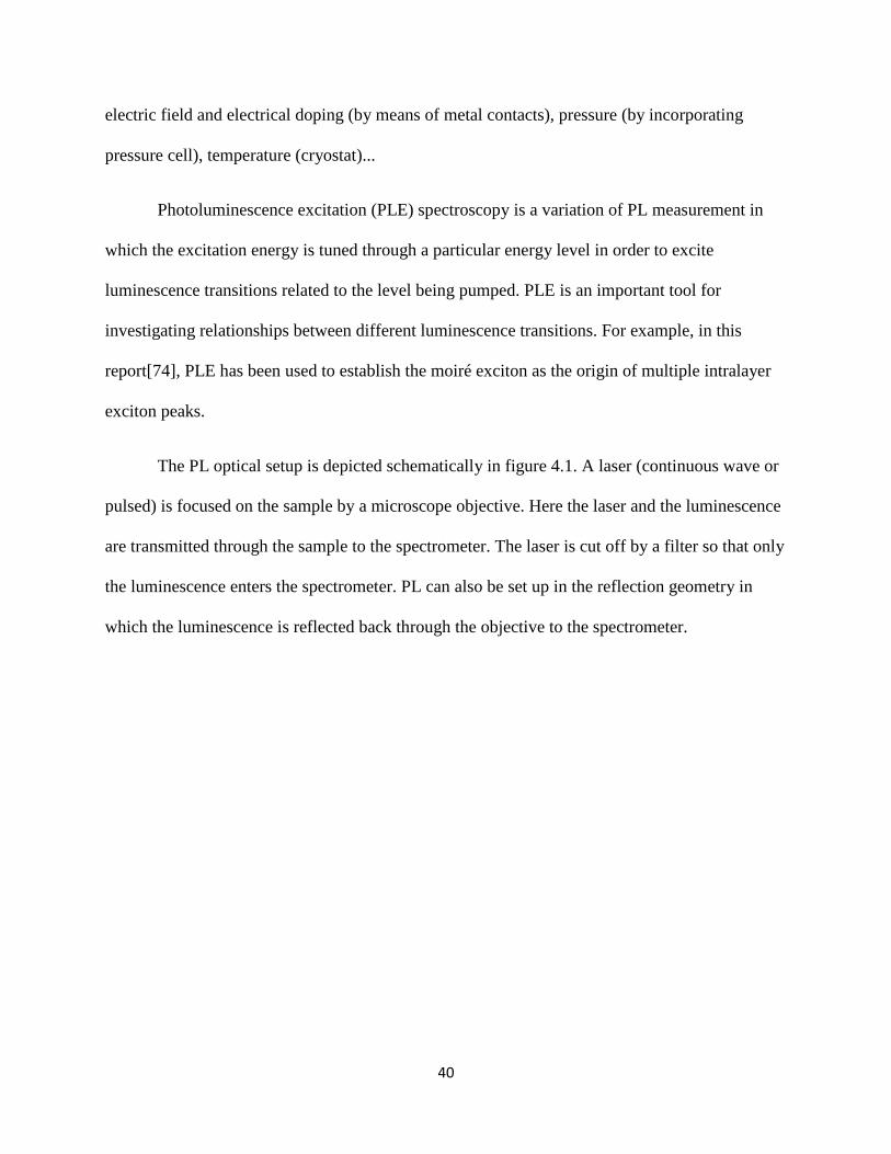
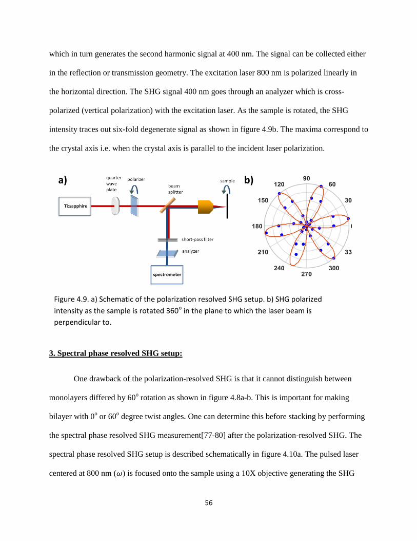
The PL optical setup is depicted schematically in figure 41 A laser (continuous wave or
pulsed) is focused on the sample by a microscope objective Here the laser and the luminescence
are transmitted through the sample to the spectrometer The laser is cut off by a filter so that only
the luminescence enters the spectrometer PL can also be set up in the reflection geometry in
which the luminescence is reflected back through the objective to the spectrometer
41
II White light absorption measurement
The white light absorption measures the absorption spectrum of a particular sample ie
how much light the sample absorbs as a function of photon energy This is different from PL
which measures how much light the sample emits Because some electronic and excitonic states
might only absorb without emitting (continuum states higher excited state) while other states
only emit instead of absorbing light (defect states) comparing PL and absorption spectra can
give valuable information about nature of different energy levels within the sample
The white light absorption setup is very similar to the PL setup (figure 41) except instead
of a laser a broadband white light source is used The white light is then focused on to the
Figure 41 Schematic of the photoluminescencewhite light absorption optical setup
42
sample and the transmission spectrum is revealed by the spectrometer subsequently Also the
wavelength filter is removed because the spectrum should not be cut off The transmission
spectra when the white light going through the sample (Tsamp) and when the white light only
going through the substrate (Tsub) are collected The absorption spectrum is calculated as
III Pump probe spectroscopy
1 Working principle
The pump probe spectroscopy is a very common type of ultrafast laser spectroscopy
There are variations of different types of pump probe In its simplest form the output pulse train
of an ultrafast laser is split into two optical paths (see figure 42) The difference in path lengths
of two beams can be changed by a mechanical delay stage which in turn controls the relative
arrival of the pulses on the sample The pump pulse is filtered out by either a polarizer or a
spectrometer after transmitted through the sample Only the probe pulse is measured by the
detector
43
Briefly the pump probe technique measures the transient absorption of the sample The
idea is that absorbing the pump decreases the samples capability to absorb the probe Recall that
the pump is completely blocked from entering the detector the probe intensity is monitored as a
function of the delay stage ie the relative arrival at the sample between the pump and the probe
The pump probe signal is defined by the difference in probe intensity with the pump present and
the probe intensity without the pump present
Where T(T0) is the intensity of the probe with(without) the presence of the pump The probe is
detected through a single channel detector connected to a lock-in amplifier We will discuss in
detail the lock-in detection technique later on in this chapter
Figure 42 Simplest form of pump probe technique Two pulses split from the Ti-sapphire
out with variable delays between them interact co-linearly with the sample The intensity
of the probe is monitored as a function of the delay while the pump is filtered out before
the detector
Sample
in
cryostat
PumpProbeTime
Delay
50-X
QWP
Filter Probe
Ti-Sapph
Laser
Detector
44
The beauty of the pump probe technique is that the temporal resolution is determined by
the pulse duration and is not affected by the slow (~ nanosecond) single channel detectors
response The measurement temporal resolution is only limited by how broad the pulse widths
are when the pulse interacts with the sample Due to optical dispersion the pulse gets broader
and broader as it passes through optics with the finite index of refraction (lenses polarizers
waveplates ) By the time the pulse reaches the sample its width might be orders of
magnitude longer than the pulse width output of the laser cavity Thus it is important to
characterize the pulse width where the sample is located for it is determined how fast the
dynamics process of the sample we can measure The measurement of the pulse duration is
called auto-correlation and is discussed in more details later
2 Two color pump probe technique
We have discussed above that pump probe is analogous to transient absorption
measurement in which the delay between pump and probe pulses reveals the absorption overtime
of particular resonances ie trion and exciton Different resonances of the sample have different
dynamics due to differences in physical properties Degenerate pump probe in which the pump
photon energy equals the probe energy can be used to measure the dynamics of exciton and trion
separately However measurements of interaction between these quasi-particles cannot be
performed Degenerate pump probe thus has certain limitations in measuring interesting
interaction phenomena
Two color pump probe technique (figure 43) allows one to measure couplinginteraction
between resonances based on the fact that the pump and probe photon energies can be tuned
independently using grating based pulse shapers Using this technique one can for example
45
pumping on the exciton(trion) and probing on the trion(exciton) thus revealing important
dynamics about trionexciton coupling In addition two color pump probe technique can be used
to probe relaxation pathways In the following sub-sections we will discuss in details different
components that make up the two color pump probe optical setup
a Pulse shaper
The scanning range of the pump and probe wavelengths is limited by the bandwidth of
the pulsed laser In the case of the Tisapphire laser this range is about 30 nm for both pump and
probe pulse shaper Figure 44 describes the working principle of a pulse shaper It consists of a
diffraction grating a focusing lens a mirror and a movable slit First the output pulse train of a
Tisapphire laser (indicated by a big gray arrow in figure 44) is diffracted by the diffraction
Figure 43 Two color pump probe optical setup In addition to the simple pump probe in
the previous figure the pulse shapers are inserted to independently vary the wavelength
or photon energy of two pulses
46
grating which causes its spectrum to spread out in the spatial dimension A focusing mirror
collimates this 1st order diffracting light on to a mirror which sends the diffracting light back on
to its original path The distance between the diffraction grating and the lens is equal to that of
the lens and the mirror which is also the focal length of the lens For the setup in the lab we use
a 20 cm lens To select pulses with different photon energies a narrow movable slit is positioned
right in front of the mirror The width of the slit determines how broad the spectral bandwidth of
the pulse is which ultimately determines the spectral resolution of the measurement Typically
we choose the slit such that it gives the spectral resolution of 1 nm Broader slits however are
available and can be interchanged for broader bandwidth pulse with more optical power The
selected pulse (red color in figure 44) is then reflected back through the lens This selected pulse
will be caught by a small circular mirror and sent on the way to the sample Because of the
optical dispersion the pulse width coming out of the pulse shaper is broader than the input pulse
width as indicated in figure 43 Thus we sacrifice the temporal resolution for the corresponding
increase in spectral resolution
47
b Acousto-optic modulator (AOM)
The next optical component on the laser path (figure 45) is the AOM or acousto optic
modulator The AOMs (manufactured by Gooch-Housego) main component is the crystalline
tellurium dioxide and offers high-frequency modulation which is around megahertz regime
instead of kilohertz modulation of the mechanical chopper Briefly an RF (radio frequency)
carrier wave ( depending on the phonon frequency of the AOM crystal) is mixed
with the modulation wave The RF mixed signal drives a piezoelectric transducer
which effectively shakes the AOM crystal at the RF mixed frequency This shaking creates a
traveling sound wave within the AOM with trough and crest of varying index of refraction The
input laser is diffracted from this grating of the sound wave such that its intensity is modulated
by the modulation frequency (figure 45) The deflection angle of the refracted beam from the
input beam can be adjusted through varying the carrier frequency ie
Figure 44 Schematic details the working principle of the pulse shaper in two color pump
probe setup
48
For the pump probe setup in our lab we modulate both the pump and probe beams using
the AOMs The pump(probe) is modulated at 175(178) MHz The carrier frequencies for the
pump and probe AOMs are 80 and 81 MHz respectively The probe carrier and modulation as
well as the pump modulation RF signals are generated by Novatech Instruments model 409B
The pump carrier signal is however generated by separate device HP 8656B The modulation
signal is mixed with a carrier signal and then is amplified before transferring to the AOMs The
lock-in detects the pump probe signal at the difference in modulation frequency between pump
and probe AOMs or 30 kHz
c Lock-in detection technique
The working principle of a lockin amplifier is illustrated in figure 46 A lockin can
extract a signal up to a million times smaller than the noisy background The lockin works by
looking for the pure signal oscillating at the reference frequency in a noisy background In other
words it locks on to the reference frequency to extract the pure signal oscillating at that
frequency In our case the noisy signal (S) comes from the balance detector which monitors the
Figure 45 Schematic of the RF (radio frequency) generation and AOM (acousto-optic
modulator)
49
probe intensity The reference signal (R) is a sinusoidal function oscillating at the difference
between pump and probe modulation ie 30 kHz from the Novatech generator
How does the lockin extract the pure signal The reference frequency(R) is multiplied by
the noisy signal (S) and integrated over the chosen time interval t0 Consider the total signal
which is a function of multiple different frequency components input into the
lockin The desired signal (pure signal) oscillates at the difference frequency Then
the output of the lockin will have the form
where is the reference signal The result is a DC signal with contributions only
from signal components oscillating at the reference frequency Signal components at all other
frequencies average out to zero The integration time t0 is very long compared with the sample
rate of the lockin in order to average over slowly varying noise Typically we choose t0 to be
100 milliseconds or 300 milliseconds Further signal improvement can be achieved using passive
bandpass filters These filters are built-in the lockin For example to detect signal at 30 kHz we
use bandpass filters from 10 kHz to 100 kHz which help to improve the signal to noise ratio
tremendously These filters also help to block the probe signal which oscillating at 178 MHz
from overloading the lockin
50
Finally to illustrate the lockin detection technique we will look at a very simple
derivation The signal entering the detector is the intensity of the probe which is the function of
the intensity of the pump (because whether the sample absorbs the pump will change the
intensity of the probe)
where S(t) is the signal entering the detector is the probe(pump) intensity Since the
pump is modulated at frequency becomes
Expand S(t) only up to first order
where is the oscillation amplitude of the probe(pump) Here we also recall that the
probe is modulated at Thus our signal becomes
Figure 46 Schematic of lockin amplifier illustrating signal (S) and reference frequency (R)
convolution using the integrator
51
Since the lockin only picks up the term at frequency The signal output of the lockin
is proportional to
Since the change in the probe intensity is small this term becomes
which is the pump probe signal
d Drift control of the sample inside the cryostat
TMD sample has lots of spatial inhomogeneity due to bubbles and residues accumulated
during the fabrication process That is small regions have a different optical signal from the rest
Thus it is important to limit our studies to a particular region of the sample Unfortunately there
is a thermal drift of the sample when it is cold This motion is random and is due to temperature
variation within the cryostat Thus it is crucial that we utilize a drift control that can correct for
this random motion from time to time
The drift control program is based on Labview image recognition software which can
recognize a pattern within an image and can extract the pattern coordinate within the image
When the selected pattern within the white light image is first chosen its initial coordinate (in
term of pixel number) is recorded Later on Labview looks for the selected pattern again and
extract its current coordinate Based on the difference between the current and the initial
coordinates Labview tells the mechanical stage on which the microscope objective is mounted to
52
move and correct for this difference If no difference is detected the stage doesnrsquot move
Labview corrects for drift every 5 seconds This time can be increased or decreased depending
on how much the sample is drifted during the measurement
2 Auto-correlation measurement
As mention in the beginning measuring the pulse duration at the sample location is very
important in characterizing the temporal resolution of the pump probe setup Since the response
of the electronics is very slow in order of nanoseconds we cant rely on them to measure the
pulse duration The autocorrelation measurement is to use the pulse to measure itself The
autocorrelation setup is almost identical to the two color pump probe setup except two-photon
detector is used in place of the sample The basic idea is to convert a measurement in the time
domain into a measurement in the space domain by increasing the path length of the pump with
Figure 47 Schematic of the autocorrelation setup to measure the pulse duration
53
respect to the probe by mean of a delay stage[26] Since the speed of light is 30 m100 fs in free
space it is easy to measure the pulse duration as short as few femtoseconds by precisely control
the delay distance with submicron accuracy The two-photon absorption detector connected to
lockin modulation yields the autocorrelation signal proportional to the temporal overlap of the
pump and probe pulses
where Ipu(Ipr) is the pump and probe intensities tD is the delay time between the two pulses Here
we assume that the two pulses have the symmetrical and identical shape (gaussian) and same
duration The width of the I(tD) divided by is the pulse duration
II Second Harmonic Generation (SHG) techniques
We use the second harmonic generation (SHG) signal from the TMD monolayer to
determine its crystal axis ie which direction is zigzagarmchair This information is critical to
making TMD heterostructures with various twist angles There are two types of SHG techniques
polarization-resolved SHG and spectral phase resolved SHG The polarization resolved
technique can determine the direction of zigzag and armchair of a monolayer Since monolayer
TMD has three-fold rotational symmetry aligning two zigzag or two armchair directions of two
monolayers will lead to either zero or 60 degrees stacking angle The spectral phase resolved
SHG completely specifies the crystal axes of monolayers which in turn determines 0o or 60
o
twist angle
1 Introduction to SHG
54
The optical response of a material is expressed in terms of the macroscopic polarization
When the optical power is small the relationship between the polarization and the incident
electric field is linear
where is the linear susceptibility Most of the optical phenomena can be described using
this linear relation A typical example is the familiar index of refraction which is given by
When the incident optical power increases the behavior of the sample deviates from the
linear regime The response of the material can now be described as a Taylor expansion of the
material polarization in powers of the electric field
In this section we will restrict ourselves to the discussion of the second order optical
response The incident electric field can always be written in term of plane waves
We obtain the second harmonic response of the form
is a third rank tensor In 3 dimensional space each index can be x y or z direction Thus
the tensor has components in total Most often this number is reduced For
example due to the commutative property of tensor contraction ie
the
number of distinct components becomes 18 Furthermore geometrical symmetry within a
55
specified crystal reduces this number further Eventually it is the symmetry information
contained in
that reveals the crystal axis of our monolayer
For monolayer TMD with the trigonal prismatic crystal structure
has only 4 non
zero components If we define the coordinate system as shown in figure 46 then these 4
components are
They give rise to different SHG signal polarizations depending on the crystal orientation
2 Polarization-resolved SHG setup
The polarization-resolved SHG is for determining the crystal axis of the monolayer
TMD The setup has been described in ref [7576] and is shown schematically in figure 49a
Briefly the output pulse train at 800 nm of a tisapphire laser is focused on to the monolayer
Figure 48 a) Monolayer TMD crystal axis b) Same as in a) but rotated 60o clockwise or
counter clockwise 120o rotation will make the crystal structure identical to a)
Xrsquo
Yrsquo
Chalcogen atom
Metal atom
a) b)
56
which in turn generates the second harmonic signal at 400 nm The signal can be collected either
in the reflection or transmission geometry The excitation laser 800 nm is polarized linearly in
the horizontal direction The SHG signal 400 nm goes through an analyzer which is cross-
polarized (vertical polarization) with the excitation laser As the sample is rotated the SHG
intensity traces out six-fold degenerate signal as shown in figure 49b The maxima correspond to
the crystal axis ie when the crystal axis is parallel to the incident laser polarization
3 Spectral phase resolved SHG setup
One drawback of the polarization-resolved SHG is that it cannot distinguish between
monolayers differed by 60o rotation as shown in figure 48a-b This is important for making
bilayer with 0o or 60
o degree twist angles One can determine this before stacking by performing
the spectral phase resolved SHG measurement[77-80] after the polarization-resolved SHG The
spectral phase resolved SHG setup is described schematically in figure 410a The pulsed laser
centered at 800 nm ( ) is focused onto the sample using a 10X objective generating the SHG
Figure 49 a) Schematic of the polarization resolved SHG setup b) SHG polarized
intensity as the sample is rotated 360o in the plane to which the laser beam is
perpendicular to
b)a)
57
signal at 400 nm ( ) The laser power at the sample is kept about 5 mW with a 5 spot size
A beta barium borate (BBO) crystal generating a reference SHG signal ( ref) is positioned
right after the sample which is put on a standard microscope slide Because the group velocity of
the fundamental pulse ( ) is faster than that for the SHG pulse ( ) as they travel through the
sample substrate and the microscope slide the fundamental will arrive at the BBO crystal first
As a result the generated ref pulse precedes the sample by a delay time Δ which
depends on how much glass between the monolayer and the crystal through which the laser
pulses travels We find that the ~1 mm thickness of an amorphous SiO2 microscope slide gives
rise to 12 nm fringes in the interference spectrum between the ref and the sample pulses
shown in figure 410b-c Thicker glass or additional optics between the monolayer and the BBO
crystal causes larger time delay Δ and more finely spaced fringes rendering the SHG
interference undetectable During the measurement the BBO crystal orientation is fixed First
the SHG interference between monolayer WSe2 and the BBO crystal is measured in which the
WSe2 zigzag direction (determined in polarization-resolved SHG) is aligned in the horizontal
direction Similarly the monolayer MoSe2 SHG phase-resolved spectra are taken with its zigzag
direction aligned horizontally Two interference spectra are plotted on top of each other for
comparison If the spectra are in phase (out of phase) as shown in figure 410b (figure 410c) the
two stacked monolayers will have near 0o (60
o) twist angle
58
4 SHG signal calculation
In this subsection we briefly derive the SHG signal detected in the polarization SHG
measurement We see the reason why full rotation of the sample yield six-fold degenerate SHG
signal (figure 48b) and why the maxima correspond to the crystal axis First of all let define our
coordinate systems XOY(XOY) is the lab(sample) frame of reference Since our excitation
laser is polarized in the x-direction the SHG summation
only contain one
term for both
and
ie
Figure 410 a) Schematic of the spectral phase resolved SHG setup b) SHG phase
resolved spectra between the monolayers and the BBO crystal with signal in phase for a
near twist angle stacking c) Similar to b) but with out-of-phase signals for a near
twist angle
a)
c)B
BO
cry
stal
sam
ple
Tisapphire
sho
rt-p
ass
filt
er
spectrometer
2ω
ref
Co
llim
atin
g le
ns
2ω
sam
ple
ω
10
X o
bje
ctiv
e
t
b)
59
Since we only know the components of
in the sample coordinate system we need to do the
tensor transformation
We are all very familiar with vector rotation which is a 1st rank tensor transformation
The relationship between vectors in XOY and XOY coordinates can be written as
This sum can be expressed in the matrix multiplication form
We therefore have identified the components of the transformation matrix being
The 3rd rank tensor transformation of
is similar to the above only has more terms in
the sum It is the relation
The sum for a particular component of
consists of only 4 terms instead of 27 because most of the components of
are zeros which
are discussed in the previous subsection Carrying out the summation for
we obtain
The transformation of
is very similar Thus the electric fields of SHG polarized in the x
and y directions are respectively
60
The intensity of SHG is the square of Px and Py Thus the polarization-resolved SHG is six-fold
degenerate Furthermore if which means the armchair is aligned with the horizontal
direction SHG signal is minimized in the x-direction and maximized in the y-direction We then
have a way to tell the crystal orientation of the monolayer
Figure 411 Coordinate systems used in SHG signal calculation XOY is the lab frame of
reference in which OX(OY) is the horizontal(vertical) direction XOY is the sample frame
of reference in which OX(OY) is the armchair(zigzag) direction Angle between OX and
OX is
61
Chapter 5 Steady-state valley properties and valley dynamics of monolayer
TMD
In this chapter we will take a look at two studies of monolayer TMD coming from our
group They are published as Physical Review B 96 041302(R) (2017) and Physical Review
Letter 117 257402 (2016) respectively
I Disorder-dependent valley properties in monolayer WSe2
We investigate the effect on disorder potential on exciton valley polarization and valley
coherence in monolayer WSe2 By analyzing polarization properties of photoluminescence the
valley coherence (VC) and valley polarization (VP) is quantified across the inhomogeneously
broadened exciton resonance We find that disorder plays a critical role in the exciton VC while
minimally affecting VP For different monolayer samples with the disorder characterized by their
Stokes Shift (SS) VC decreases in samples with higher SS while VP again remains unchanged
These two methods consistently demonstrate that VC as defined by the degree of linearly
polarized photoluminescence is more sensitive to disorder potential motivating further
theoretical studies
1 Motivation
Valley refers to energy extrema in electronic band structures Valley pseudo-spin in
atomically thin semiconductors has been proposed and pursued as an alternative information
carrier analogous to charge and spin [353781-84] In monolayer transition metal
dichalcogenides (TMDs) optical properties are dominated by excitons (bound electron-hole
pairs) with exceptionally large binding energy and oscillator strength [332] These excitons form
62
at the energy extrema ( ) points at the Brillouin zone boundary thus inheriting the ( )
valley index Valley contrasting optical selection rules make it possible to optically access and
control the valley index via exciton resonances as demonstrated in valley specific dynamic Stark
effect [85-87] as an example
For valleytronic applications particularly in the context of using valley as an information
carrier understanding both valley polarization and valley coherence are critical Valley
polarization represents the fidelity of writing information in the valley index while valley
coherence determines the ability to optically manipulate the valley index Earlier experiments
have demonstrated a high degree of valley polarization in photoluminescence (PL) experiments
on some monolayer TMDs (eg MoS2 and WSe2) suggesting the valley polarization is
maintained before excitons recombine [12378384] Very recently coherent nonlinear optical
experiments have revealed a rapid loss of exciton valley coherence (~ 100 fs) due to the intrinsic
electron-hole exchange interaction in WSe2 [47] In fact the ultrafast dynamics associated with
the valley depolarization (~ 1 ps) [44] and the even faster exciton recombination (~ 200 fs)
[7388] extracted from the nonlinear experiments are consistent with the PL experiments As
long as the valley depolarization and decoherence occurs on time scales longer or comparable
with exciton recombination lifetime steady-state PL signal shall preserve polarization properties
reflecting the valley-specific excitations
It is important to ask the question if disorder potential influences valley polarization and
coherence considering the fact that there are still a significant amount of defects and impurities
in these atomically thin materials This critical question has been largely overlooked in previous
studies Here we investigate how valley polarization and coherence change in the presence of
disorder potential First valley coherence is observed to change systematically across the
63
inhomogeneously broadened exciton resonance while there are no observable changes in valley
polarization We suggest that this systematic change is related to exciton localization by disorder
potential where the low energy side of the exciton resonance corresponds to weakly localized
excitons and the high energy side is associated with more delocalized excitons [5189]
Furthermore we investigated a number of monolayer WSe2 samples with different defect density
characterized by the Stokes shift between the exciton peak in photoluminescence and absorption
A higher degree of valley coherence is observed in samples with a smaller Stokes shift or lower
defect density [9091] These two observations consistently suggest that shallow disorder
potential reduces valley coherence without influencing valley polarization appreciably Our
studies suggest that a more qualitative evaluation of valley coherence may guide the extensive
on-going efforts in searching for materials with robust valley properties
2 Background
Figure 51 a) The band structure of monolayer WSe2 at two degenerate K and K valleys Valley contrasting spins allow left (right) circular polarized light to excite excitons in the K (K) valley b) Bloch Sphere representation of valley pseudospin degree of freedom Circular polarized light prepares an exciton in |Kgt or |Kgt state ie states at the poles whereas linear polarized light prepares an exciton in a superposition of |Kgt and |Kgt ie states at the equator
|Kgt
|Krsquogt
b)
K Krsquo
a)
64
The low energy bands with associated spin configurations in monolayer WSe2 are
illustrated in figure 51a A dipole allowed (ie an optically bright) transition can only occur if
the electron in the conduction and the missing electron in the valence band have parallel spins
Thus the transition between the lowest conduction band and the highest valence band is dipole
forbidden and the lowest energy exciton transition is between the second conduction band and
the highest valence band as illustrated in figure 51a Using ( ) polarized excitation light
excitons are preferentially created in the ( ) valley due to the valley contrasting optical
selection rules [35] As with any binary degree of freedom K and Krsquo valleys can be represented
as a vector on a Bloch sphere as shown in figure 51b The degree of valley polarization is
defined by the normalized difference in cross-circular and co-circular signals as
(1)
where represents co (cross) circular polarized PL intensity with respect to the
excitation polarization Previous studies on monolayer WSe2 have reported a large valley
polarization in steady-state PL experiments [124783] suggesting that valley scattering rate is
slower or comparable with exciton population recombination rate In the Bloch sphere picture a
large VP suggests that once the Bloch vector is initialized along the north pole it retains its
orientation during exciton population recombination time On the other hand when a linearly
polarized excitation laser is used a coherent superposition of two valley excitons is created [11]
Such a coherent superposition state corresponds to a Bloch vector on the equatorial circle
Previous experiments suggest that exciton valley coherence can be monitored by the linearly
polarized PL signal [92] Here we follow this method and further quantify the degree of valley
coherence by the following definition
65
(2)
where represents co (cross) linear polarized PL intensity with respect to the excitation
polarization
3 Steady-state photoluminescence measurements
We first investigate the change of VC and VP as a function of energy across the exciton
resonance on a mechanically exfoliated monolayer WSe2 sample It is known that the degree of
valley polarization depends strongly on the excitation wavelength [1193] In our experiments
the excitation energy is chosen to be energetically close to the exciton resonance to observe a
finite degree of VC but far enough so that resonant Raman scattering does not interfere with VC
[1193] Unless mentioned otherwise for all PL measurements presented in this manuscript we
use a continuous wave laser at 188 eV (ie 660 nm) and keep the power ~ 20 microW at the sample
with a focused spot size of ~ 2 microm diameter A typical PL spectrum of monolayer WSe2 is
shown in Figure 52a with two spectrally well-resolved resonances corresponding to exciton and
trion (a charged exciton) respectively There are two additional resonances at the lower energy
which may be due to either dark states or impurity bound states [41] Here we focus on valley
physics associated with the exciton resonance shaded in blue
66
Figure 52 a) PL spectrum of monolayer WSe2 excited with 188 eV CW laser Blue shaded Gaussian represents the fits to the exciton resonance b) Zoomed in spectrum around the exciton resonance shows co (cross) linear PL signal with respect to the excitation laser polarization Corresponding VC is plotted on the right hand side c) PL spectra taken with co- and cross- circular PL signal with respect to a circularly polarized excitation laser PL intensity and VP are plotted on the left and right vertical axes respectively
1660 1680 1700 1720 1740 1760Energy (meV)
1
a08
a06
a04
a02
a0
PL
In
tensity
(au
)a)
1730 1740 1750 1760
025
a020
a015
a010
a005
a0
1
a08
a06
a04
a02
a0
Energy (meV)
PL In
tensity
(au
)
Va
lley
Co
here
nce
co linear
cross linear
VC
b)
1
a08
a06
a04
a02
a0
Va
lley
Po
lariza
tio
n
PL
In
tensity
(au
)
co circular
cross circular
VP
Energy (meV)
025
a020
a015
a010
a005
a0
1730 1740 1750 1760
c)
67
Figure 52b plots the co- and cross-linear polarized PL and the corresponding VC across
the exciton resonance The VC drops to zero beyond the lower energy edge of the exciton
resonance due to the presence of the trion which cannot exhibit VC in PL spectra due to photon-
spin entanglement [11] Interestingly we observe a monotonic increase of the VC across the
inhomogeneously broadened exciton resonance with varying from 0 to 035 as shown in
Figure 52b This monotonic change in VC across the exciton resonance is qualitatively repeated
on all measured samples VC reaches the maximum value at the high energy side of the exciton
and approaches zero at the low energy end Beyond the high energy side of the exciton
resonance because of low signal VC plateaus and becomes noisy We suggest that the increase
of VC across the exciton resonance arise from the degree of exciton localization [519495]
Valley coherence associated with the delocalized excitons is more robust than the weakly
localized excitons
In contrast VP remains constant across the exciton resonance with ~ 048 as
illustrated in Figure 52c It has been suggested that only atomically sharp potentials can induce
inter-valley scattering and depolarization of valley exciton [11] Thus the invariability of the VP
suggests that the inhomogeneously broadened exciton resonance is mainly due to slowly varying
spatial potentials (in contrast to atomically sharp potentials) Such disorder potential may be
attributed to local strain as well as shallow impurity potentials [519495] This speculation is
also consistent with the observation that strongly localized excitons likely due to deep
atomically sharp potentials appear at much lower energy ~ 100-200 meV below the exciton
resonance[9697] An important mechanism causing valley depolarization is electron-hole
exchange unaffected by shallow potential fluctuations [98-100] Other valley scattering
68
mechanisms such as Dyakanov-Perel (DP) and Eliott-Yafet (EY) mechanisms are slower and
considered unimportant for excitons in TMDs [98]
4 Correlation of VC and VP versus Stokes Shift
To further investigate the role of disorder potential on valley properties we studied a
total of 6 monolayer WSe2 samples prepared with both CVD (chemical vapor deposition) and
mechanical exfoliation We quantify the defect density using the spectral shift between exciton
resonances measured in PL and absorption known as the Stokes shift (SS) As a simple method
based entirely on commonly used linear optical spectroscopy methods SS has been used to
characterize a wide variety of material systems [90101] including defect density [102-104]
monolayer fluctuations in quantum wells [91105106] and size distribution in quantum dots
[107108]
A typical SS measurement is shown in figure 53a The PL and white light absorption
spectra of the same exfoliated monolayer WSe2 are taken at 13K Briefly the absorption
spectrum is taken using a broadband white light source in the transmission geometry to minimize
reflection induced spectral line-shape changes To achieve similar spot sizes in both absorption
and PL measurements a 100 m pinhole is placed in the focal plane between two focusing
lenses in the white light path to optimize the spatial mode The absorption spectrum is plotted as
a differential and normalized spectrum where is the transmission through the
substrate and is the transmission through both the substrate and monolayer sample The
exciton resonances in the PL and absorption are fitted with Gaussian functions The peaks
extracted from the fittings are indicated by the dotted lines yielding a 48 meV SS for this
sample
69
To quantify the dependence of valley properties on SS (and on defect potentials) the
above measurements are repeated on all 6 samples We confirmed SS of a particular sample has
little to no temperature dependence as shown in the inset of figure 53a For comparison across
different samples the VC (or VP) value for each sample is calculated by taking the average of
the VC (or VP) in a range spanning from the exciton peak where is the fitted linewidth
We found the range of the spectral integration does not change our qualitative conclusion The
results as summarized in figure 53b have a number of interesting features Firstly VC is found
Figure 53 (color online) a) Stoke shift is shown as the difference in energy between the absorption spectrum and PL from the exciton resonance Inset SS dependence on temperature b) VC (VP) is plotted with respect to SS VC shows an inverse dependence versus SS whereas VP shows no recognizable trend
1 3 5 7 9
06
a055
a050
a045
a040
040
a035
a030
a025
a020
Va
lley
Co
here
nce
Va
lley
Po
lariza
tio
n
Stokes Shift (meV)
VC
VP
b)
1
a08
a06
a04
a02
a0
02
a015
a010
a005
a0
SS
1720 1740 1760 1780
Energy (meV)
PL
In
tensity
(au
)
Abso
rption
a)
X
SS
(m
eV
)
Temperature (K)0 40 80 300
a
5a
a
4a
a
3a
Sample E2
Sample E3
70
to decrease with increasing SS of samples with a fractional drop of ~ 25 between the samples
with the lowest to highest SS Specifically varies from 032 to 025 as SS changes from 21
meV to 86 meV Secondly VP has similar values for all the samples ( ~ 045) and no
correlation between VP and SS is observed Based on the assumption that SS is correlated with
the defect density in different samples we infer that disorder potential reduces VC but has little
influence on VP This conclusion is consistent with the spectral dependence of VC and VP
across the exciton resonance observed on a single sample as reported in figure 52b and 2c In
addition a recent experiment [94] investigated spatial variations of VP and VC on a CVD grown
monolayer WSe2 While VP was found to be mostly constant VC showed significant changes
likely arising from disorder potential
5 Conclusion
In summary we report a systematic study of the effect of shallow disorder potential on
VC and VP in monolayer WSe2 The low energy side of the exciton resonance is associated with
weakly localized excitons and the high energy side with more delocalized excitons Using
steady-state polarization resolved PL we observe that the VC monotonically increases across the
inhomogeneously broadened exciton resonance The VP on the other hand remains constant
across the exciton resonance VP and VC are then measured for samples with different SS (a
measure of disorder) We find that VC varies inversely with SS and VP remains largely
invariant Our observations suggest that shallow disorder potentials have a crucial effect on the
exciton valley coherence Particularly weakly localized excitons lose valley coherence more
rapidly than the delocalized excitons On the other hand disorder potential does not affect the
valley polarization noticeably Our work should motivate future experiments and microscopic
71
theoretical studies necessary for a comprehensive understanding of the effect of disorder on
valley properties in TMDs
6 Extended Data
a Fitting comparison of the absorption spectrum and Sample information
We have used 6 samples They are labeled CVD1 E2 E3 E4 E5 E6 where the first one
is CVD grown sample and the others are made by mechanical exfoliation The sample order is
arranged so that they are in order of increasing Stoke Shift
We have fit absorption profiles with three different lineshapes- gaussian lorentzian and
half gaussian (see figure 54) The comparison of the three methods is summarized below in
Table 61 In S2 we also show an example of the lineshape fitted with the three methods We
emphasize that the stokes shift measured with all three methods is very similar and hence does
not change our treatment and conclusions in any way
Sample Peak position (meV) FWHM (meV) Stokes Shift (SS)
L G Half-G L G Half-G L G Half-G
CVD1 17435 1744 17437 231 207 237 16 21 18
E2 17558 17558 17557 176 149 136 41 41 40
E3 17572 17573 17572 181 159 128 47 48 47
E4 17537 17537 17536 208 161 154 65 65 65
E5 17557 17566 17566 447 368 250 75 84 83
E6 17575 17575 17571 211 170 155 86 86 83
Table 61 Summary of peak positions full-width half-maximum (FWHM) and Stokes Shift (SS) using Lorentzian (L) Gaussian (G) and Half-gaussian fitting methods for different samples
72
b Stokes Shift plotted against absorption linewidth
We fit Gaussian profiles to exciton absorption spectra and plot SS versus FWHM of the
fitted Gaussian for all 8 monolayer samples (see figure 55) The vertical errorbars of SS are due
to the combined fitting errors of both PL and absorption peak The horizontal errorbars of
FWHM are small and therefore not visible on the scale plotted The correlation between SS and
FWHM is only valid on a certain range of the FWHM We speculate that the lack of correlation
between the two quantities could be due to different types of defects causing inhomogeneous
broadening in different samples
Figure 54 Absorption linewidth of sample E4 fitted using different profiles Lorentz
Gauss and half Gauss
73
c Subtracting trion contribution to exciton valley coherence
The data shown in figure 56 and data figure 52 are from the same exfoliated sample
whose SS is 48 meV Here we plot the data over greater energy range to show the trion
resonances explicitly We fit the trion resonances of co and cross linear PL signals with
gaussians We then subtract the trion fitting curve from co and cross PL signals and compute the
degree of valley coherence from exciton Evidently the degree of valley coherence computed
before and after the trion subtraction is the same
Figure 55 The absorption spectra are fitted with Gaussian profile and the FWHMs are
extracted and plotted against SS
74
d Omitted data from CVD sample
Figure 56 a) Trion resonances on both co and cross signal are fitted with Gaussians Since
trion doesnt show any valley coherence the fits are essentially the same Valley coherence
is shown here before the trion subtraction from the co and cross signals b) After trion
subtraction the valley coherence is essentially the same signifying that trion has minimal
contribution to exciton valley coherence
75
Figure 57 Degree of a) valley coherence and b) valley polarization plotted across the
exciton resonance of omitted CVD sample c) Valley coherence and valley polarization
plotted against SS included the omitted data point
76
II Long-Lived Valley Polarization of Intravalley Trions in Monolayer WSe2
We investigate valley dynamics associated with trions in monolayer tungsten diselenide
(WSe2) using polarization resolved two-color pump-probe spectroscopy When tuning the pump
and probe energy across the trion resonance distinct trion valley polarization dynamics are
observed as a function of energy and attributed to the intravalley and intervalley trions in
monolayer WSe2 We observe no decay of a near-unity valley polarization associated with the
intravalley trions during sim 25 ps while the valley polarization of the intervalley trions exhibits a
fast decay of sim4 ps Furthermore we show that resonant excitation is a prerequisite for
observing the long-lived valley polarization associated with the intravalley trion The
exceptionally robust valley polarization associated with resonantly created intravalley trions
discovered here may be explored for future valleytronic applications such as valley Hall effects
1 Motivation
The valley degree of freedom (DoF) indices the crystal momentum of a local energy
minimum within the electronic band structure and has been proposed as an alternative
information carrier analogous to charge and spin [35] In atomically thin transition metal
dichalcogenides (TMDs) fundamental optical excitations excitons (electron-hole pairs) and
trions (charged excitons) are formed at the hexagonal Brillouin zone boundaries at the K (K )
points As such they inherit the valley index which is locked with electron spins in TMDs Thus
exciton and trion resonances allow optical access and manipulation of the valley DoF in TMDs
using circularly polarized light [81237109110] The exceptionally large binding energies of
these quasiparticles (ie 200ndash500 meV for excitons and an additional binding energy of 20ndash40
meV for trions) further promise room temperature valleytronic applications
77
[58536573109111-113] High-efficiency valley initialization and a long lifetime of valley
polarization are preferred in valleytronic applications [46114-116] Initial experiments based on
steady-state photoluminescence have shown the possibility of creating a near unity valley
polarization in MoS2 and WSe2 via exciton resonances [1112] Time-resolved measurements
soon revealed that exciton valley polarization is quickly lost (sim1 ps) due to intrinsic electron-
hole exchange interaction The large exciton valley polarization observed in the steady-state PL
results from the competition between the valley depolarization time (sim1 ps) and the exciton
population relaxation time (sim100ndash200 fs) [7388] On the other hand trions offer an interesting
alternative route for optical manipulation of the valley index for a number of reasons First in
contrast to the ultrafast exciton population relaxation time trions exhibit an extended population
relaxation time of tens of picoseconds in monolayer TMDs [117-124] Second trions as charged
quasiparticles influence both transport and optical properties of TMDs and may be readily
detected and manipulated in experiments such as valley Hall effect [82] Last but not least
previous studies of negatively charged trions in conventional doped semiconductors suggest that
negatively charged trions leave the background electron gas spinpolarized after the electron-hole
recombination [99125-128] Thus trions may play a particularly important role in manipulating
electron spins and the valley DoF
2 Background
In this report we investigate valley polarization dynamics associated with negatively
charged trions in monolayer WSe2 using polarization resolved two-color pump-probe
spectroscopy with sub-nm spectral resolution Distinct valley polarization dynamics were
observed as the resonant pump-probe energy is tuned across the trion resonance and attributed to
the two types of trions known to exist in monolayer WSe2 intravalley and intervalley trions In
78
particular we discover a long-lived near-unity valley polarization (≫25 ps) associated with the
resonantly created intravalley trions This exceptionally robust valley polarization (in
comparison to excitons and intervalley trions) originates from the peculiar requirement of
simultaneous transfer of three carriers (two electrons and one hole) to the other valley with
proper spin and crystal momentum changes When the pump energy is tuned to the exciton
resonance the long-lived trion valley polarization dynamics can no longer be observed
highlighting the difficulty in accessing intrinsic trion valley dynamics under nonresonant
excitation conditions used in the majority of previous experiments [109129] The discovery of
an exceptionally robust trion valley polarization is significant since it suggests that information
encoded in the valley index can be stored and manipulated electrically via effects such as valley
Hall effect over long time scales
In monolayer WSe2 the particular band structure and optical selection rules suggest that
the energetically lowest interband transition is dipole forbidden [4198130] as illustrated in
figure 58(a) Thus two types of negatively charged trions intravalley and intervalley may form
represented with symbols T|1gt and T|2gt respectively The two electrons have the opposite
(same) spins for intravalley trions T|1gt (intervalley trions T|2gt) Because of the different spin
configurations the diagonal exchange interaction present in the intervalley trions T|2gt lifts the
energy degeneracy and leads to a shift of sim6 meV relative to the intravalley trions T|1gt as
illustrated in figure 58(a)[96131] The exciton resonance is approximately 30 meV higher than
T|2gt which has implications for optical phonon-assisted scattering between T|2gt and exciton
resonances [5493]
3 Experimental Method
79
We study a mechanically exfoliated monolayer WSe2 flake on a sapphire substrate (kept
at temperature sim13 K) using a pump-probe setup (see description in chapter 5) The sample is
considered to be n-doped based on similarly prepared samples from previous studies [1196]
The output from a mode-locked Ti-sapphire laser is split into pump and probe beams whose
wavelengths are independently varied by two grating-based pulse shapers After the pulse
shapers the pulse duration is sim1 ps (with sim07 nm bandwidth) After passing through linear
polarizers and 1 4 λ wave plates for circular polarization control the beams are focused to a spot
size of sim2 m The power for each beam is kept at sim10 W to obtain nonlinear signals in the χ(3)
regime and to avoid heating effects The transmitted differential transmission (DT) signal is
detected following further spectral filtering through a spectrometer which allows us to study
trion dynamics under resonant excitation conditions DT is defined as DT = (Tpump onminus Tpump
off)Tpump off where Tpump off(on) is the transmitted probe intensity when the pump is off (on) and it
measures the third-order nonlinear response
3 Experimental Results
We first performed a fully degenerate experiment using cross-linearly polarized pump-
probe beams to identify exciton and trion resonances at 1753 and 1719 meV respectively as
shown in figure 58(b) We note that intravalley and intervalley trions are not spectrally resolved
in our sample as those on BN substrates [54] Nevertheless both types of trions are intrinsic to
WSe2 and should be present under the inhomogeneously broadened trion resonance
80
a Quasi-resonance pump probe scans
We then investigate the trion valley dynamics by simultaneously tuning the pump-probe
energy across the trion resonance The pump energy is kept at 2 meV above the probe energy to
allow filtering of the scattered pump after passing through the spectrometer This quasiresonant
excitation condition is referred to as the resonant excitation condition in this paper for simplicity
In the following a σ+ polarized pump pulse is used to populate the K valley and the subsequent
dynamics in the K (K ) valley is investigated using a σ+ (σminus) polarized probe pulse The co- and
cross circularly polarized DT signals are displayed in the same panel as a function of time delay
Figure 58 (a) Possible configurations of charged and neutral bright excitons in WSe2 (b)
Differential transmission spectrum of WSe2 (dots) The black line is an interpolation curve
serving as a guide to the eye The solid Gaussians illustrate the spectral position of the
exciton and the two trion (inter- and intravalley) resonances The spectral positions of
probe energies for data in figure 59 and 610 (dashed colored lines) and the pump energy
for figure 510 (gray line) are also illustrated
81
between the two pulses as shown in Figs 2(a)ndash(c) The co-circular experiments reflect trion
population relaxations within the same valley and have similar features in all scans after an
initial rise during the excitation pulse (solid grey area) there is a relatively fast decay of a few
picoseconds followed by a slower decay of sim35 ps The observed biexponential decay is
consistent with previous experiments and likely arises from scattering between the bright trion
states and dark states (or trap states) [117] The most intriguing feature is the drastic and
systematic change in the cross-circularly polarized scans as the pump probe energies are tuned
through the trion resonance as shown in Figs 2(a)ndash(c) In cross-circularly polarized experiments
trions created in the K valley are converted to trions in the K valley via spin flip and electron-
hole exchange interaction We attribute the dynamics on the higher (lower) energy side of the
trion resonance to intervalley trions T|2gt (intravalley trions T|1gt) For intervalley trions T|2gt
probed at 17244 meV the population in the opposite valley builds up and reaches its maximum
value after a few picoseconds [figure 59(a)] In contrast valley scattering is minimal for
intravalley trions T|1gt probed at 17196 meV during trion population relaxation time as shown in
figure 59(c) The robust valley polarization associated with T|1gt is reflected in the minimal
cross circularly polarized signal shown in figure 59 (c) As the excitation energy is tuned further
to the lower energy negative DT signal appeared only for the cross-circularly polarized scans
This negative DT signal for cross-circularly polarized scan likely arises from valley-dependent
many-body effects[120132133] We limit the following discussion to the spectral region with
only positive DT signal where the valley polarization can be defined meaningfully
We define valley polarization as VP =(co minus cross)(co + cross) following earlier work on
TMDs [12134] and calculate trion valley polarization for two particular probe energies at 17244
and 17196 meV respectively We focus on these two energies to highlight the distinct trion
82
valley dynamics associated with the two types of trions while minimizing spectral overlap
between them Trion valley polarization at these two energies as a function of time delay
between the pump and probe is shown in figure 59 (d) The valley polarization is only plotted
over a limited delay range because the error bars become very large at larger delays due to the
small DT signal in both the co- and cross circularly polarized scans The intervalley trion valley
polarization T|2gt exhibits a fast decay of sim4 ps which is consistent with earlier studies [117] In
contrast the valley polarization associated with the intravalley trion T|1gt persists much longer
and decays with a time constant much larger (gt25 ps) than the experimental observation range A
valley depolarization time longer than the population relaxation time associated with the
intravalley trions means that these trions recombine before valley scattering occurs leaving the
residual electron valley or spin polarized
83
b Non-resonant pumping of trions
Figure 59 Co- (solid dots) and cross-polarized (open dots) signals recorded in resonant
excitation experiments across the trion resonance at probe energies of (a) 17268 meV (b)
1722 meV and (c) 17196 meV (d) Valley polarization for the measurements displayed in
(a) and (c)
84
This long-lived trion valley polarization associated with T|1gt is only observable under
resonant excitation conditions When we excited the mobile excitons at the higher energy side of
the exciton resonance (17588 meV specifically) while tuning the probe energy within the trion
resonance the difference between valley polarization dynamics for T|1gt and T|2gt disappears as
shown in figure 510(a)ndash(c) An apparent fast valley depolarization (sim2 ps) is observed for probe
energy tuned to both types of trions as shown in figure 510 (d) These experiments performed
under the nonresonant excitation conditions do not report on the intrinsic trion valley dynamics
Instead it is necessary to consider a number of physical processes including the valley
depolarization of excitons trion formation and phase space filling in the interpretation The key
feature of similar and rapid valley depolarization for probing at both trions mainly arises from
the rapid exciton valley depolarization ie excitons created at the K valley quickly scatter to the
K valley within the pulse duration (sim1 ps) due to electron-hole exchange interaction [4799]
The same DT signal amplitude in the co- and cross-circularly polarized experiments after 5 ps
support the interpretation of equal trion populations at the two valleys In the co-circular
experiments the DT reaches its maximal value immediately after the excitation pulse The
creation of excitons at the K valley prohibits the formation of either type of trions in the same
valley due to phase space filling leading to an instant and reduced absorption at the trion energy
In the cross-circular experiments the finite DT signal rise time (1ndash2 ps) is determined by the
time for the exciton to capture an extra charge ie the trion formation time [51] These
experiments unequivocally illustrate the importance of near-resonant excitation to access the
intrinsic dynamics associated with the trion valley DoF
85
4 Summary
Figure 510 Co- (solid dots) and cross-polarized (open dots) signals recorded in
nonresonant excitation experiments for pumping at the exciton resonance and probing at
(a) 17244 meV (b) 1722 meV and (c) 17196 meV (d) Valley polarization for the
measurements displayed in (a) and (c)
86
We summarize the various exciton and trion conversion and valley dynamics in a
diagram shown in figure 511 The top of the diagram illustrates the rapid exciton valley
depolarization (sim1 ps and shorter than the excitation pulses used in our experiments) due to
electron-hole exchange interaction Trion valley depolarization is expected to be slower than that
associated with excitons because it requires an additional carrier spin flip Interestingly the
drastically different valley polarization dynamics associated with the two types of trions in WSe2
have never been explicitly proposed or observed experimentally The K valley T|2gt can scatter to
the opposite valley and form K valley T|2gt without loss of energy This process however is not
as efficient as scattering to K valley T|1gt The latter process occurs through electron-hole
exchange interaction and is energetically favorable Thus we suggest that this K valley T|2gt to
K valley T|1gt conversion process is responsible for the sim4 ps intervalley trion valley
depolarization observed Intervalley trions created in the K valley can also be converted to
intravalley trion (the vertical dashed arrow) in the same valley via a spin flip which is likely a
slower process as illustrated by the vertical dashed lines Finally intravalley trion valley
depolarization is long-lived as illustrated in the bottom of the diagram The transfer of either a
single electron or an electron-hole pair to the other valley transforms the intravalley trion into an
intervalley trion which is an energetically unfavorable process Scattering of K valley T|1gt to
the opposite valley requires the simultaneous transfer of three carriers (two electrons and a hole)
to the other valley Thus valley polarization of the intravalley trions in monolayer WSe2 is
exceptionally stable consistent with our experimental observations Valley polarized PL from
the trion resonance was previously observed under nonresonant excitation conditions in MoS2
[109] In addition to being different TMD materials various time scales (population relaxation
valley depolarization and trion formation) are manifested differently in PL and DT experiments
87
Systematic studies are necessary to investigate how these time scales vary among different TMD
samples placed on various substrates at different doping levels
Microscopic theory of valley dynamics associated with trions with different spin
configurations and exchange interaction is not available yet The experiments presented here
provide further motivation and challenges for such theoretical studies on valley dependent
exchange interaction and many-body effects due to Coulomb interaction which is particularly
pronounced in monolayer semiconductors Most importantly this work suggests a possible
approach for creating and manipulating long-lived valley DoF potentially useful in valleytronic
applications
Figure 511 Schematic of the suggested valley polarization dynamics exciton and trion
conversion processes and their respective time scales as measured in the experiment
Dashed lines suggest that such processes are possible in principle but do not compete
favorably with other faster processes
88
Chapter 6 Evidence for Moireacute excitons in van der Waal heterostructure
In this chapter we look at a paper from our group that first reports the influence of the
Moireacute potential on optical signal of van der Waal heterostructure Our study has been published
as Nature 567 71ndash75 (2019)
Recent advances in isolating and stacking monolayers of van der Waals (vdW) materials
have provided a new approach for creating quantum materials in the ultimate two-dimensional
limit[135136] In vdW heterostructures formed by stacking two monolayer semiconductors
lattice mismatch or rotational misalignment introduces an in-plane moireacute superlattice[9] While it
is widely recognized that a moireacute superlattice can modulate the electronic band structure and lead
to novel transport properties including unconventional superconductivity[137] and insulating
behavior driven by correlations[7071138] its influence on optical properties has not been
investigated experimentally Here we report the observation of multiple interlayer exciton
resonances with either positive or negative circularly polarized emission in a MoSe2WSe2
heterobilayer with a small twist angle We attribute these resonances to the excitonic ground and
excited states confined within the moireacute potential The twist angle dependence recombination
dynamics and temperature dependence of these interlayer exciton resonances all support this
interpretation These results suggest the feasibility of engineering artificial excitonic crystals
using vdW heterostructures for nanophotonics and quantum information applications
I Motivation
In vdW materials the usual constraint of lattice matching between adjacent layers is
lifted enabling different types of materials to be stacked to form atomically thin heterostructures
The twist angle between two layers can be adjusted arbitrarily in contrast to conventional
89
epitaxially grown heterostructures in which the orientation of adjacent layers is fixed by the
crystal axes These unique properties of vdW heterostructures present new possibilities for
engineering electronic band structure and optical properties via an in-plane moireacute superlattice
When two monolayers of semiconducting transition metal dichalcogenides (TMDs) are stacked
vertically a moireacute superlattice is not necessarily present The lattice constants of TMDs that
share common chalcogen atoms (eg MoX2 and WX2) only differ by ~01 In rotationally
aligned MoSe2WSe2 heterobilayers (hBLs) grown by chemical vapor deposition (CVD)
methods the minor lattice distortion in each layer leads to a commensurate atomic alignment
without a moireacute pattern[139] In mechanically stacked hBLs however a twist angle between the
two layers is most often present Thus a moireacute pattern is expected and has indeed been directly
imaged with high-resolution transmission electron microscopy[140]
In TMD hBLs with a typical type-II band alignment[5557141] rapid charge transfer[63]
of electrons and holes to different layers following optical excitation leads to emission from the
lower-energy interlayer exciton transitions[13142] Theoretically multiple interlayer exciton
resonances are expected to form due to the lateral confinement from the moireacute potential (figure
61)[5960143] The interlayer coupling determines the depth of the moireacute potential which is
predicted to be ~100-200 meV by first-principles calculations in TMD hBLs (see figure 65) and
confirmed by scanning tunneling spectroscopy experiments on a rotationally aligned MoS2WSe2
bilayer grown by CVD[9] Such a deep potential is expected to localize interlayer excitons as
long as the moireacute supercell has a period on the order of 10 nm or larger[5960] If and how the
moireacute potential manifests in far-field diffraction-limited optical measurements remains an
outstanding question
90
Here we report the observation of multiple interlayer exciton (IX) resonances in a high-
quality hexagonal boron nitride (hBN) encapsulated MoSe2WSe2 hBL Because the layers are
aligned with a small twist angle and the inhomogeneous spectral linewidths are reduced with the
capping layers several nearly equally spaced IX resonances are spectrally resolved at low
temperature Upon excitation with circularly polarized light the IX resonances exhibit
alternating co- and cross-circularly polarized photoluminescence (PL) We suggest that the
alternating polarized emission originates from the atomic-scale spatial variations of the optical
selection rules within a moireacute supercell The energy spacing and twist-angle dependence of the
resonances and helicity of the emitted light are consistent with calculations of multiple IX states
confined within a moireacute potential with ~150 meV lateral confinement in agreement with first-
principles calculations Time-resolved and temperature-dependent PL measurements support this
assignment of the ground and excited state IX excitons
II Moireacute theory overview
We first describe conceptually how the moireacute potential may give rise to multiple exciton
resonances with different optical selection rules as shown in figure 61 In MoSe2WSe2 hBLs
with a small twist angle ~1deg the exciton Bohr radius is large compared to the monolayer lattice
constant but small relative to the moireacute period (~20 nm) Thus the interlayer exciton can be
described as a particle moving in a slowly varying moireacute potential[60144] Within a moireacute
supercell there are three points where the local atomic registration preserves the three-fold
rotational symmetry as shown in Figs 1a and 1b These three sites are denoted by
respectively where
refers to -type stacking with the site of the MoSe2 layer aligning
with the hexagon center ( ) of the WSe2 layer These high symmetry points are local energy
extrema within the moireacute supercell where excitons can be localized In the case of sufficiently
91
deep energy modulation the moireacute pattern can provide an array of identical quantum dot
potential (left panel of figure 61c)
Another important consequence of the moireacute pattern is to impose spatially varying optical
selection rules[6066] Although the valley degree of freedom is still a good quantum number for
interlayer excitons the optical selection rules of exciton resonances are no longer locked to the
valley index as is the case of monolayers As shown in figure 61b an exciton residing directly at
site (
) only couples to ( ) polarized light Site has a dipole oriented perpendicular
to the plane which does not efficiently couple to normal incident light (see Methods) The
optical selection rules are determined not only by atomic quantum numbers but also by the
relative position between tungsten and molybdenum atoms in real space It is the latter
dependence that is responsible for distinct selection rules at different positions with the moireacute
supercell The optical selection rules change continuously in the moireacute pattern and are generally
elliptically polarized (right panel of figure 61c)
92
Figure 61 (a) Different local atomic alignments occur in an MoSe2WSe2 vertical heterostructure with small twist angle The three highlighted regions correspond to local atomic configurations with three-fold rotational symmetry (b) In the K valley interlayer exciton transitions occur between spin-up conduction-band electrons in the MoSe2 layer and spin-up valence-band electrons in the WSe2 layer K-valley excitons obey different optical selection rules depending on the atomic configuration
within the moireacute
pattern refers to -type stacking with the site of the MoSe2 layer aligning with the
hexagon center ( ) of the WSe2 layer Exciton emission at the (
) is left-circularly (right-circularly) polarized Emission from site
is dipole-forbidden for normal incidence (c) Left
The moireacute potential of the interlayer exciton transition showing a local minimum at site
Right Spatial map of the optical selection rules for K-valley excitons The high-symmetry points are circularly polarized and regions between are elliptically polarized
a
b
W atom Mo atom Se atom
σ+
K
K
σ-
K
K
K
K
c
-100 -50 0 50
Moireacute potential (meV)
-1 0 1
Degree ofcircular polarization
93
III Sample Details and Experimental Method
To examine the influence of the moireacute potential on interlayer excitons we perform
micro-PL measurements on multiple MoSe2WSe2 hBLs The samples were prepared following a
mechanical exfoliation and transfer process[145] We will focus on one encapsulated hBL with
1deg twist angle unless otherwise stated (see figure 67) An optical microscope image is shown in
figure 62a The hBL is held at 15 K and excited with a continuous wave 660 nm laser with a
full-width at a half-maximum spot size of 15 microm For an uncapped sample the PL spectrum
(dashed curve in figure 62b) features intra-layer neutral and charged excitons and a broad IX
resonance consistent with earlier reports[13146147] When the hBL is encapsulated between
hBN layers four spectrally resolved IX resonances emerge (solid curve in figure 62b) due to
reduced inhomogeneous broadening The IX spectral region is replotted in the lower panel of
figure 63a and fit with four Gaussian functions The central emission energies extracted from the
fits are 1311 meV 1335 meV 1355 meV and 1377 meV The resonance energies are
repeatable across different locations on the hBL with a nearly constant peak spacing of 22plusmn2
meV (figure 63b) Some moderate inhomogeneous broadening remains possibly due to multiple
moireacute domains or small variations in strain and layer spacing within the excitation spot that
covers ~1000 moireacute supercells
Multiple IX peaks may be indicative of quantized energy levels due to the lateral
confinement imposed by the moireacute potential as predicted in the calculations below The fact that
the resonances span an energy range of ~70 meV suggests that the moireacute potential depth is on the
order of 100 meVmdashsufficient to justify the picture of an array of quantum dot potential
Polarization-resolved PL experiments provide additional compelling evidence in support of this
interpretation Using polarized excitation we collected co- ( detection) and cross-circularly
94
( detection) polarized PL spectra which are shown in figure 63c We define the circular
polarization of emission as
where is the measured PL intensity We plot as a
function of energy in figure 63d The IX resonances exhibit a variation of between 02 and -
02 A negative indicates that the PL signal with cross-circular polarization is stronger than
that from the co-circular polarization We propose that the alternating co- and cross-circular
emission arises from the unique spatial variation of the optical selection rules predicted based on
rotational symmetry considerations[60]
To relate the observed PL signal to the optical selection rules we first assume that the
above-gap -polarized light optically creates spin-polarized intralayer excitons in the MoSe2
and WSe2 monolayers primarily in the K valley This spin-valley locking in TMD monolayers
has been established by previous studies[1236110] Second we assume that the charge transfer
process leading to the IX formation conserves the valley and spin index which is supported by a
previous polarization-resolved pump-probe spectroscopy[77] It then follows that an IX state
created in the K valley following optical excitation emits ( ) polarized light if it is
localized near the (
) high-symmetry point within the moireacute potential landscape (refer to
Figs 1b and 1c) We show in the calculations below for a deep moireacute potential that confines
excitons at the site the wave functions associated with the quantized exciton states can
acquire additional angular momentum and sample the potential landscape in a way that leads to
multiple resonances with alternating and light emissionmdasha characteristic consistent with
our experimental observations Because the valley relaxation and charge transfer dynamics can
be very complex the above assumptions do not strictly hold leading to reduced below unity
Because observing the alternating circular selection rules of IX resonances requires that the
valley polarization time is longer or comparable to IX recombination lifetimes[12] valley-
95
conserving PL can only be observed in bilayers with the smallest twist angle that exhibit
relatively short IX recombination lifetimes (~ 1 ns)
Figure 62 (a) Optical image of an hBN-encapsulated MoSe2WSe2 stacked heterostructure The hBL region is indicated inside the black dotted line (b) Comparison of the photoluminescence spectrum from an uncapped heterostructure (dashed curve) and an hBN-encapsulated heterostructure (solid curve) Neutral (X0) and charged (X-) exciton emission is observed from the MoSe2 and WSe2 monolayers The interlayer exciton (IX) emission is observed ~300 meV below the intralayer resonances (c) Illustrative band diagram showing the type-II alignment and the IX transition
a c
b
WSe2
MoSe2
- --
+++
IX
10 microm
1L WSe2
1L MoSe2
hBL
Emission Energy (meV)1300 1400 1500 1600 1700
PL Inte
nsity (
arb
units)
1
08
06
04
02
0
IX
hBN encapsulated
uncapped
X0
X-
X0
WSe2MoSe2
96
IV Moireacute exciton model
Here we provide a detailed description of the theory which has some overlap with the
main text The full theory can be found in Ref [59] In the moireacute pattern the local band gap
varies in real space and acts as a periodic potential for excitons IXs can be viewed as a
wavepacket moving in the potential with a center-of-mass (COM) motion described by
where is an energy constant is the COM kinetic energy is the moireacute
potential energy and is the exciton mass For IXs in a WSe2MoSe2 hBL where
Figure 63 (a) Representative PL spectra shown for hBLs with 1deg and 2deg twist angles Each spectrum is fit with four (1deg) or five (2deg) Gaussian functions (b) The center energy of each peak obtained from the fits at different spatial positions across each sample The average peak spacing increases from 22 plusmn 2 meV to 27 plusmn 3 meV with twist angle (c) Circularly polarized PL spectrum for + excitation of the 1deg sample (d) The degree of circular polarization versus emission wavelength obtained from the spectra in (c)
97
is the electron bare mass is a smooth potential and is approximated by the lowest-order
harmonic expansion where are the first-shell moireacute reciprocal lattice vectors The parameter
is the energy scale of the potential while determines where the potential extrema are
located We choose to be such that the potential minima are located at sites The
motivation of this choice is to be consistent with experimental observation as lowest-energy
excitons confined by the potential near site have an s-wave symmetry COM wave function
and emit light at the K valley Near sites the potential has the form of a harmonic
oscillator
where is the moireacute period An exciton confined
in this potential has quantized energy levels
where are non-
negative integers We take the twist angle to be resulting in of ~19 nm To be consistent
with the experimentally observed energy spacing (~25 meV) we take to be 18 meV The
overall range of the potential variation is meV
Both K and -K valley excitons are governed by the Hamiltonian in Eqn 1 but they have
different optical responses due to valley-dependent optical selection rules Below we focus on K
valley excitonsmdashproperties of -K valley excitons can be inferred by using time-reversal
symmetry Following the convention used in Ref [59] the bright IXs are located at the moireacute
Brillouin zone corners The optical matrix element for the bright IXs at the K valley is
98
where is the semiconductor ground state of the heterobilayer is the IX state is the in-
plane current operator and is the system area In the integral of Eqn 3 is the periodic
part of the Bloch wave state and captures the position dependence of the optical
matrix element in the moireacute pattern In Eqn 4 and represent the
components The spatial dependence is given by and
where are constants and | | is about 133
[60] At a generic position has both and components There are three notable
positions with high symmetry At the site ( ) vanishes and has a purely
component In contrast at site (
) has a purely component Finally
vanishes at site (
) These local optical selection rules are illustrated in Figs 1b and
1c of the main text The spatial variation of is plotted in Extended Data Figs 3c-d Around
site ( ) is nearly a constant while has a vortex structure
Based on Eqns 1-4 we calculate the theoretical optical conductivity of IXs at the K valley as
shown in figure 64b of the main text We have chosen such that the lowest-energy IX has
the experimental energy 1310 meV Four resonances with alternating valley optical selection
rules appear in the energy window shown in figure 64b Both the energies and helicities of these
resonances agree with the experimental observation The corresponding exciton COM wave
function can be understood as Bloch wave states composed of Wannier functions confined to the
potential minimum position ( sites) We show for the four peaks in figure 64c-f For
peak (1) has s-wave symmetry centered at sites and the integral in Eqn 3 only
acquires the components in In peak (2) the Wannier function associated with is
still centered at a site but it has a chiral p-wave form with an additional angular momentum
99
compared to Due to this difference peak (2) has the opposite valley optical selection rule
with respect to peak (1) The behavior of peaks (3) and (4) which have d-wave and f-wave
forms can be understood in a similar way
As expected our model calculation cannot reproduce all experimental features such as
the linewidths and relative intensity between the IX resonances For example the PL intensity of
the excited states is higher than the ground state a feature that may originate from disorder and
has been previously observed in an ensemble self-assembled quantum dots[148] The assignment
of the observed IX peaks as ground and excited states localized near the moireacute potential
minimum is consistent with the measured thermal behavior and recombination dynamics (see
figure 66)
100
V First-principles calculation of the bandgaps of MoSe2-WSe2 bilayer heterostructure
We employ the density function theory (DFT) with the Perdew-Burke-Ernzerh (PBE)
exchange-correlation functional including spin-orbit coupling (SOC) to calculate the electronic
structure of three specific stacking styles within the moireacute superlattices in a twisted MoSe2-WSe2
hBL (figure 65) The interlayer van der Waals (vdW) interaction is included within the DFT-D2
functional implemented in the Vienna ab initio simulation package (VASP) package[149150]
Figure 64 (a) Illustration of the spatial variation of the moireacute potential and the confined multiple IX resonances (b) Optical conductivity of IXs in the K valley in response to (blue line) and (red line) polarized light (c)-(f) Real-space map of the center-of-mass wave functions for peaks (1) (2) (3) and (4) respectively (g)-(h) The spatial variation of the components of the optical matrix elements
a
hf g
101
The cutoff of plane-wave energy is set to be 500 eV with a 16x16x1 k-point sampling in the
reciprocal space The atomic structures are calculated with a perpendicular vacuum larger than
18 angstroms which is enough to avoid artificial interactions between adjacent supercells
Because of the strong SOC splitting at the K-K point the band structures of the three stacking
types exhibit a direct bandgap at the K-K point as shown in figure 65 Therefore without
considering phonons we expect the lowest-energy interlayer exciton to be a direct exciton
Figure 65 shows the relaxed interlayer distances and bandgap values which are substantially
different with different stacking types and sensitive to the interlayer couplings vdW interaction
is the consequence of dynamical correlation effects which may not be well captured by DFT To
evaluate possible variations we perform additional calculations using another vdW functional
the DFT-D3 in which the interlayer distances and band gaps are different Despite different
choices of vdW functionals the band gaps vary more than 100 meV from different stacking
types within the moireacute superlattice ie a deep moireacute potential is consistently found in the first-
principle calculations Since electron self-energy corrections and excitonic effects are known to
dominate quasiparticle band gaps and optical spectra of 2D semiconductors we have applied the
first-principles GW-Bethe-Salpeter Equation (BSE) to obtain the energy of the lowest
exciton[151] The quasiparticle energies are calculated by the single-shot G0W0 approximation
using the general plasmon pole model We use a k-point grid of 24x24x1 for calculating the e-h
interaction kernel and a k-point grid of 48times48times1 for converged excitonic states These GW-BSE
simulations are performed using the BerkeleyGW code with the slab Coulomb truncation
included It is found that the exciton binding energy varies less than 5 within the moireacute
supercell Our calculations also confirm that the moireacute potential depth (ie quasiparticle gap)
102
in H-stacked samples (~20 meV) is significantly reduced compared to R-stacked samples (gt100
meV)
VI Thermal behavior and recombination dynamics
We show the steady-state PL at elevated temperatures between 25 K and 70 K in figure
66 With increasing temperature the rate at which the intensity of the two highest-energy peaks
decreases is significantly faster than the lower-energy peaks Because excitons in the excited
states are less-confined within the moireacute pattern they are more susceptible to phonon-induced
activation out of the potential[152] Excitons in the excited states can also relax to the lower
energy states which can enhance the recombination rate from these transitions Indeed we
Figure 65 (a) The three stacking types (
) of the bilayer MoSe2-WSe2
heterostructure and corresponding DFT-calculated band structures (b) Interlayer distance and the band gap of three stacking types (c) First principles GW-BSE calculation results for quasiparticle band gap and exciton binding energy for different stacking types
PBE-D2 PBE-D3
Stacking
W-Mo Interlayer Distance (Aring) 708 644 646 711 652 651
Gap at K (eV) 105 093 1047 1082 1032 1144
Stacking
Quasiparticle band gap (eV) 158 156 158 158 151 162
Exciton energy (eV) 117 117 120 120 112 122
b
c
a
103
observe a faster decay of the excited states shown by the time-resolved PL dynamics in figure
66b The dynamics of the highest energy peak are fit by a single exponential with a 09 ns time
constant As the emission energy decreases the dynamics become slower and biexponential
approaching decay times of 2 ns and 10 ns for the lowest energy state The slight increase in the
fast and slow decay times with decreasing energy shown in the inset to figure 66b is often
observed in other systems with spatially localized excitons such as in self-assembled InAsGaAs
quantum dots[153]
Figure 66 (a) Temperature dependence of the PL between 25 K and 70 K (b) Time-resolved PL dynamics (points) at energies near the four IX transitions labeled in the inset The solid lines are biexponential fits to the data The inset shows the emission energy dependence of the fast and slow decay times
a
b
PL
Inte
nsi
ty (
arb
un
its)
10aa
08
a
06
a
04
a
02
a
01250 1300 1350 1400 1450
Emission Energy (meV)
25 K 70 K
0 5 10 15 20 25Time (ns)
100
10-1
10-2
PL
Inte
nsi
ty (
arb
un
its)
Life
tim
e (n
s) 101
100
Energy (meV)1300 1350 1400
104
VII Additional heterostructures with interlayer exciton splitting R-type samples
Here we give additional details about sample 1 (1o twist angle) and sample 2 (2
o twist
angle) presented in the main text The Gaussian fit of the sample 2 PL spectrum shows the
emergence of five IX peaks 1306 meV 1336 meV 1366 meV 1386 meV and 1413 meV
The average energy spacing of sample 2 is 27 plusmn3 meV which is slightly larger than the spacing
in sample 1 If we fit this spacing for sample 2 with our model calculation using the same 162
meV moireacute potential as for sample 1 we obtain a twist angle of 14o from the fit This value is
within our estimated uncertainty in determining the angle via the optical microscope image of the
heterostructure A larger twist angle causes the lowest energy transition in a TMD hBL to
become more indirect in momentum space20
leading to a longer recombination lifetime Indeed
we observe slower time-resolved PL dynamics for sample 2 shown in figure 67 Fitting the
time-resolved PL curves with a single exponential function yields time constants of 195 ns and
896 ns for samples 1 and 2 respectively
105
VIII Additional heterostructures with interlayer exciton splitting H-type samples
We fabricated an H-type hBL (ie 60o twist angle) that shows two IX peaks at 1356 meV
and 1395 meV (figure 68) The energy separation between peaks is 40 meV which is consistent
with previous reports of hBN encapsulated H-type MoSe2WSe2 hBLs3132
Our theoretical model
predicts that the moireacute potential is on the order of 10-20 meV for H-type hBLs which is too
small to lead to the observed splitting 40 meV In hBLs with -type stacking (near 60deg twist
angle) the observation of two IX resonances separated by 25-50 meV has been attributed to
momentum indirect transitions3132
which is consistent with the spectrum of our H-type sample
(figure 68)
Figure 67 (a) Steady state PL spectra from 1o sample (sample 1) and 2o sample (sample 2) (b) Time-resolved PL dynamics for IX emission at 1320 meV as indicated by the shaded area in (a)
a b
sample 1 (1o)
sample 2 (2o)P
L inte
nsity (
norm
aliz
ed)
PL inte
nsity (
norm
aliz
ed)
Energy (meV) Time (ns)
sample 1 (1o)
sample 2 (2o)
1250 1300 1350 1400 1450 -10 0 10 20 30 40 50 60
100
10-1
10-2
106
IX Photoluminescence emission from Sz = 1 and Sz = 0 exciton transitions
A recent theoretical study has also proposed IX resonances arising from
transitions which are optically dark in monolayers but become bright in hBLs[68] Although we
cannot completely rule out states as a possible explanation for some of the observed
resonances we argue below that such an explanation is less likely for the higher-energy states
observed in our study which are less-stable states at a higher temperature and exhibit a shorter
lifetime compared to the lower-energy resonances In an -type heterostructure exciton
recombination is predicted to emit left- (right-) circularly polarized light at the (
) atomic
configurations Since the exciton at the K point consists of a spin-down conduction band
electron and spin-up valence band electron (see Fig 1b of the main text) it emits at an energy
higher than that of the states by the conduction band spin splitting of ~30 meV (see Ref
Figure 68 Comparison between IX resonances from H-type sample (upper panel) and R-type sample (lower panel)
R type (1o)
H type (60o)P
L Inte
nsity
(norm
aliz
ed)
1250 1300 1350 1400 1450
Emission Energy (meV)
107
[154]) With increasing temperature thermalization of excitons might lead to enhanced emission
from states which is inconsistent with the temperature dependence of the excited states
shown in Fig 5a of the main text The states are expected to have longer recombination
lifetimes than the states due to a weaker transition dipole moment[68] which is contrary
to the trends in the measured lifetimes in Fig 5b of the main text We can also rule out the Sz = 0
z-polarized transition since our 50X objective has small NA number (042) compared to much
higher NA number (082) objective used to detect the z-polarized dark exciton in TMD
monolayer reported in the previous work[43] Therefore we suppress excitation and collection of
these states by an additional order of magnitude compared to the in-plane transitions as shown
experimentally in the supplemental material of Ref [43]
X Outlook and conclusion
To control moireacute excitons a natural choice would be to tune the moireacute period through the
twist angle Indeed in another hBL with a small twist angle of ~2deg we observe multiple IX
resonances spaced by 27plusmn3 meVmdashlarger than the spacing for the 1deg sample as expected (see
figure 63) While systematic studies of the twist angle dependence of IX in TMD hBLs have
been performed for large (~5deg) steps[1067] the broad inhomogeneous linewidth has precluded
the effect of the moireacute potential to be observed An applied electric field or magnetic field may
also allow one to tune the IX properties Previous experiments have reported IXs exhibit a Stark
shift as a function of the electric field[155] or a Zeeman splitting as a function of the magnetic
field[147155] Other recent experiments have also reported multiple interlayer exciton
resonances However these experiments were performed on samples either with different
stacking conditions[155156] (see figure 68)
or with significantly broader IX inhomogeneous
linewidths that mask any effects of the moireacute potential[1067] We also discuss the possible
108
contribution from transitions (see Methods) which are optically dark in monolayers but
become bright in hBLs
In summary we observed multiple interlayer exciton resonances in an hBN-encapsulated
MoSe2WSe2 heterobilayer The key spectroscopic features observed in our experimentsmdashfour
IX resonances with alternating circularly polarized PL systematic changes in the lifetime with
energy and the temperature dependencemdashare naturally explained by assuming the presence of
the moireacute superlattice expected to exist in a stacked hBL In multiple samples with slightly
different twist angles we have observed systematic changes in IX energy spacing and lifetimes
which is consistent with the effect of the moireacute potential Multiple IX resonances originating
from phonon replicas[157] momentum-space indirect transitions[156] or states are
possible in TMD bilayers however we consider them less likely explanations in the samples
investigated here based on the arguments discussed in the main text and Methods section Future
experiments capable of resolving individual IXs confined within a supercell using either near-
field optical probe or combined scanning tunneling spectroscopy and optical spectroscopy
studies will be most valuable to further establish the influence of the moireacute potential
109
Chapter 7 Conclusion and outlook
In this dissertation wersquove briefly discussed exciton properties of monolayer TMD
namely the strong binding energy giving rise to short lifetime due to the reduced dielectric
screening the extremely short valley coherence and valley polarization (less than 1ps) due to
electron-hole exchange interaction One way to extend those timescales up to 4 orders of
magnitude is to create TMD heterostructure with interlayer exciton We discussed in extension
the properties of the interlayer exciton in heterostructures with various twist angles Due to the
spatial indirect nature of the interlayer exciton its lifetime and valley polarization can be 10-100
nanoseconds
We further discuss our method for creating high-quality monolayer TMD and
heterostructure to the best of our knowledge in the appendix Since sample fabrication is an
empirical process our tips and tricks are accumulated over the years by many undergrads and
graduate students working on creating samples Admittedly our fabrication method is not
perfect More work needs to be done in order to further improve sample quality indicated by the
reduced low-temperature exciton linewidth Nevertheless our method should be a very good
starting point for new members of the group who wish to fabricate samples
With the improved sample quality we have successfully created TMD heterostructures
with interlayer Moireacute excitons in MoSe2WSe2 heterobilayer which possess extremely intriguing
optical properties Particularly different exciton excited states confined within the Moireacute
potential exhibit alternating polarization due to the spatial variation of optical selection rule It is
also this property that we can pinpoint the origin of our multiple interlayer exciton peaks
observed in low-temperature photoluminescence Our study of the Moireacute excitons is the first
110
experimental evidence of Moireacute effect on the optical properties of van der Waal heterostructure
It has changed peoples perspective on TMD heterostructure Since our paper is published on
Arxiv various research groups have claimed evidence for intralayer Moireacute excitons in
MoS2MoSe2[158] and WS2WSe2[74] heterobilayers Another group has claimed optical
signature for trapped interlayer Moireacute excitons in MoSe2WSe2[159] Another study reports the
hybridization between the interlayer and intralayer excitons due to moireacute potential in WS2MoSe2
heterobilayers[160] More importantly recent pump-probe study also reports multiple interlayer
excitons resonances in the WS2WSe2 heterobilayer [161]with either conserving or reversing
circular polarization
The fact that the Moireacute superlattice defines a regular array of quantum dot potentials and
localizes the quasiparticles offers exciting future studies of TMD heterostructures Because of
the unique optical selection rules associated with these quasiparticles photon spin and valleys
are naturally entangled making them an ideal platform to explore matter and photonic qubit
entanglement as an essential element for large-scale quantum information processing Yet there
are a lot of things we dont know about this system Thus we have proposed to invest
fundamental of properties of interlayer Moireacute excitons including quantum yield dipole moments
formation dynamics and dephasing mechanisms Interlayer excitons are stable at room
temperature and exhibit a long lifetime Their properties relevant to quantum information
applications remain mostly unknown These properties will be the focus of our group near future
studies Our next step would be to study the quantum dynamics of the valley index associated
with interlayer excitons As a binary quantum degree of freedom in TMDs this valley index can
represent a qubit with potentially long decoherence time due to large momentum mismatch and
the associated spin flip to the opposite valley[82162163] Demonstrating Rabi oscillations of
111
interlayer excitons is in our list for the next experiment Rabi oscillations refer to the reversal
control of electronic state occupancy by light This is a benchmark experiment in controlling a
qubit since it is equivalent to a single bit NOT gate[164-167] The confined and localized
nature of Moireacute excitons makes it more likely to realize this quantum control Lastly we will
explore spin-photon entanglement of Moireacute excitons They are excellent single photon emitters
due to the spatial confinement We will follow similar protocols[168-172] in neutral atoms
trapped ions and self-assembled quantum dots spin-photon entanglement associated with the
confined pseudospins in the Moireacute superlattice will be investigated
112
APPENDIX
Sample fabrication techniques
In this appendix we discuss the techniques of mechanical exfoliation to make monolayer
TMD and dry transfer method to stack these monolayers onto predefined pattern or onto TMD
heterostructure Well also talk about tips and tricks for making good samples and mistakes to
avoid The aim is to provide members of the Li group a reference for sample fabrication As we
constantly strive to make a better quality sample our techniques are constantly updating The
information discussed in this chapter is up to date as of November 2018
I Exfoliation
1 Materials and tools
a Tape
We use cleanroom blue tape UltraTape 1310TB100-P5D to exfoliate monolayer TMD
This tape has low adhesiveness and less residue than the common 3M Scotch tape
b PDMS (polydimethylsiloxane)
We find that exfoliating TMD directly onto the silicon substrate has a much low rate of
finding a monolayer than exfoliating onto PDMS Also a monolayer on PDMS is more
convenient for transferring and stacking heterostructure We use two types of PDMS
Commercial PMDS (figure A1b) can be purchased from GelPak The specific models are X0
and X4 PF films X4 film is stickier than X0 Home-made PDMS (see figure A1a) can be made
113
from the PDMS kit available for purchase from Amazon Search for Sylgard 184 silicone
elastomer kit How to make this type of PDMS will be discussed in the later part of this section
Type of
PDMS
Commercial Home-made
Pro Smoother surface -gt larger monolayer
size and more spatial uniformity
Thinner -gt easier for dry transfer
Stickier -gt may increase the amount
of monolayer exfoliated per hour
Con Thicker -gt more difficult for dry
transfer
Less even surface -gt monolayer tends
to have more cracks and wrinkles if
the tape is not lifted carefully
Table A1 Pros and cons of the two types of PDMS
Table V1 describes the pros and cons of the commercial and homemade PDMS Notice
that these pros and cons wont make or break the exfoliation and transfer The quality of the
fabricated sample depends more crucially on other factors For example wrinkles and cracks of
the monolayer can be minimized by lifting the blue tape carefully Monolayer size and yield rate
depend crucially on the quality of bulk TMD material
c Cell phone film
We use cell phone film to exfoliate hBN (hexagonal boron nitride) on to commercial
PDMS This type of film is commercially available on Amazon The band is Tech Armor High
Definition Clear PET film screen protector for iPhone 55C5S Exfoliating TMD using cell
phone film results in more cracks and wrinkles and smaller size monolayer than using blue tape
The procedure to exfoliate hBN on commercial PDMS will be discussed later in this chapter
114
d Materials
We have been purchasing bulk TMD from two companies 2D Semiconductor and HQ
Graphene Table V2 summarizes the pros and cons of each type
Company 2D semiconductor HQ graphene
Pro hBN encapsulated monolayer achieves
narrower linewidth at cryogenic temperature
~4 meV exciton linewidth for encapsulated
WSe2 ~3 meV exciton linewidth for
encapsulated MoSe2 (narrowest)
Very large size monolayers can be
exfoliated ~few hundred microns
(figure A1d)
Con More difficult to exfoliate than HQ graphene
bulk
Broader low-temperature exciton
PL linewidth
Table A2 Pros and cons of two commercial bulk TMDs
Narrow linewidth means that the material has less amount of impurity and defect leading
to inhomogeneous broadening Thus we mainly exfoliate 2D semiconductor bulk for optical
studies However if monolayer size becomes an important constraint andor the experiment
doesnt require narrow monolayer linewidth one may exfoliate from HQ graphene bulk
We exfoliate hBN grown by Taniguchi and Watanabe from national institute for material
science in Japan This hBN is of higher quality than the commercially available hBN
We havent worked much with graphene as a group However this will change as we
seek to add electrical contacts and an external electric field to the sample in the future Graphene
or few-layer graphite is ideal to apply vertical electric field because they are transparent
conductors Experience from our collaborator suggests that kish graphite yields the largest
115
graphene flake because it has a large grain size Kish graphite with various qualities can be
purchased from graphene-supermarketcom with grade 300 being the highest quality
2 Exfoliation Related Procedures
We find that exfoliating on PDMS provides acceptable monolayer yield rate while maintaining a
good quality sample We avoid another exfoliation methods such as gold-assisted
exfoliation[173] although produces larger size monolayer with a higher yield rate the optical
properties of the monolayer is severely degraded We also tried to exfoliated TMD on top heated
silicon[174] but we find that this method works best for graphene only Exfoliating TMD this
way still gives a lower yield rate than our PDMS method
a TMD exfoliation procedure
Thin down the bulk TMD onto the blue tape Kayleighs tip The flakes on blue tape should
be quite thin and flaky (figure A1c) so that when lifting fair amount number of flakes
remain on the PDMS If flakes on blue tape are too thick thin down them more by contact
the flakes with another empty blue tape and then separate
Cut a small square of PDMS 1 by 1 cm and lay it flat onto the middle of the microscope
slide
For commercial PDMS make sure that the PDMS surface is flat You can do this by lifting up
the PDMS and let it slowly on top of the slide Doing it this way will cause the PDMS to be
flattened
Make contact between the TMD flakes on blue tape and the PDMS Can use a finger to press
lightly on the tape Marshalls trick imagine petting the ant under the tape One should tap
lightly and uniformly without hurting the ant
116
Lift the tape up without knee-jerk motion Lift slowly enough so that a few flakes still
remain on the PDMS but not slower Marshalls trick lift the tape like you are waving a
magic wand
Examine the PDMS under the microscope Under transmission lighting look for a layer with
the least contrast with respect to the surrounding PMDS background This is monolayer
If overall a lot of flakes are still quite thick you can use another empty blue tape to make
contact with the flakes on PDMS Then lightly lift off and look again The process can be
repeated number of times usually no more than thrice If you still get no monolayer it is
better to move on exfoliating new flakes
b Preparation and storage of bulk material
Bulk material is stored inside containers within a plastic bag in the vacuum chamber
Figure A1 a) and b) Home-made (thicker film) and commercial PDMS (thinner film) on
microscope slide respectively c) Bulk TMD thinned down on a piece of blue tape One can tell
the quality of the bulk TMD by looking at the flakes Good quality bulk usually appears with flat
cleaved surface In this case the bulk is not that good but still exfoliatable d) Huge monolayer
WSe2 exfoliated on home-made PDMS
100 mm
a) b) c) d)
117
Place the bulk between 2 pieces of blue tape - press lightly to ensure bulk adheres to both
pieces of blue tape
Slowly pull apart blue tape One side should have thinner exfoliated bulk material and the
other should have the majority of the bulk material Return the majority of the bulk to the
container
Using the thinner bulk material repeatedly thin the bulk between pieces of a blue tape Try to
create bulk patterns on the blue tape so that different flakes are close together ie efficient
exfoliation
You should have ~6-8 separate pieces of blue tape with bulk ready to exfoliate onto PDMS
Keep the majority of this bulk encapsulated between 2 pieces of blue tape Only separate the
blue tape when all bulk on exposed pieces is entirely exhausted DO NOT re-encapsulate the
bulk between the blue tape unless you are thinning the material This will cause the material
to become exhausted much more quickly
c How to make home-made PDMS
Mix the silicone and the curing agent together in 101 (10) weight ratio Using a clean stick
to stir for 5 minutes After that the mixture will be full of bubbles Avoid mixing PDMS in a
glass container because you cant remove it afterward Note more curing agent (gt10)
makes the PDMS softer and stickier We found that 10 is a good ratio to make firm and flat
PDMS
Pour the mixture into plastic Petri dishes The thickness of the PDMS should be about 2 mm
118
Put the Petri dishes into a vacuum container and pump down the pressure to eliminate
bubbles The time inside the vacuum container is varied from 1 to 2 hours Make sure that the
PDMS is free of any bubble before removing from the chamber
Put the Petri dishes inside the fume hood and let the PDMS cured (hardened) in ambient air
for 24 hours before it is ready to be used
II Transfer
1 Transfer microscope
We modified a microscope to transfer our monolayers to a pre-determined structure or
stack them on top of each other The schematic of the transfer microscope is described in figure
A2a The monolayer is transferred from the microscope slide held by the slide holder onto the
substrate held by the substrate holder
The relative position of the monolayer on the microscope slide with respect to the
substrate is controlled by numbers of stages First of all the translation of the monolayer is
control by x y and z micrometers The master XY translation stage moves both the microscope
slide and substrate with respect to the microscope objective The motion of the substrate is
further controlled by the rotation stage and the tilt stage The rotation stage rotates the substrate
with respect to the monolayer on the microscope slide The range of rotation is about 2 degrees
Larger rotation can be done by moving the substrate physically Tilt stage adjusts the tilt angle
between the substrate and the PDMS This is most crucial to ensure the successful dry transfer
discussed later on in this section The tilt stage has two knobs that can tilt the substrate either
back and forth or left and right
119
Other components of the transfer microscope include the vacuum pump the heater and
the multimeter for temperature monitoring During the transfer the substrate and the microscope
slide are held in place by air suction provided by a small pump through white plastic tubing (see
figure A2b) The substrate can be heated up by a high power ceramic heater that can go up to
500oC The heater is powered by a simple DC power supply and is insulated from the
surrounding by the substrate holder and four pillars underneath which are made out of macor -
one type of machinable ceramic (figure A2b) The heater also includes a thermal couple which
can provide temperature monitoring via multimeter (yellow casing next to the microscope in
figure A2b)
2 Transfer using PPC (polypropylene carbonate) coated PDMS dot
We follow the procedure previously described in the supplementary of [175] Here the PPC acts
as a glue with temperature dependent adhesiveness Thus one can pick up or drop off (release)
layer using different temperature The pickup temperature is lower than the drop off temp The
Figure A2 a) Schematic of the transfer microscope showing different components b) Actual
picture of the microscope
XYZ translation stage for slide holder
Master XY translation stage
Tilt stage
Rotation stage
Heat insulated pillars
Substrate holder with heater
Microscope objective
Slide holder
a) b)
120
PDMS dot acts as a probe that can pick up a selected layer while leaving the surrounding flakes
intact
a How to make PDMS dot
First we need to make the PDMS mixture using the PDMS kit The procedure is previously
described in section I2c
Use a mechanical pipette draw a small amount of PDMS mixture and drop it onto a piece of
flat home-made PDMS that is previously hardened The size of the PDMS dot depends on
how large the drop is Usually the dot is about 1 to 2 mm in diameter but can be made
smaller (figure A3b)
Leave the PDMS to cure inside the fume hood for 24 hours
b How to make PPC (polypropylene carbonate)
The polypropylene carbonate in solid form can be purchased online from Sigma Aldrich
Mix PPC and anisole according to 12100 to 15100 weight ratio in a glass vial
Slowly shake the mixture for a few hours This step can be done by putting the vial on top of
a shaking plate The specific shaking speed does not matter too much We usually set the
speed to about 100 rpm (round per minute) After this step the PPC mixture becomes viscous
clear liquid (figure A3a) and is ready to be spin coated onto the PDMS dot
121
c How to spin coat PPC onto PDMS dot
Use a mechanical pipette draw a small amount of PPC inside the vial apply the PPC evenly
onto the PDMS dot Make sure that the PPC mixture is thoroughly stirred before this step
Avoid creating bubbles when dropping PPC
Put the PDMS dot into a spin coater Set the spinning speed to 3000 rpm in 60 seconds The
acceleration doesnt matter too much After this step the PPC is spread out on the surface of
the PDMS dot
Bake the PPC coated PDMS dot on a hot plate under 130oC for 5 to 10 minutes to evaporate
most of the anisole in the PPC
Let the PDMS cool down to room temperature We now ready for transfer
d Transfer procedure
i Pick up
Figure A3 a) 12 PPC liquid inside the glass vial ready to be spin coated b) PMDS dot
a) b)
122
The layers can be picked up from the home-made or commercial PDMS using PPC coated
PDMS dot
Heat the substrate to ~50oC
Slowly lower the PDMS dot by using the z micrometer in the XYZ translation stage
Approach the monolayer slowly and carefully Crashing the dot to the monolayer will
cause the layer to crack andor shatter
After the dot contact the monolayer fully lift the PDMS dot slowly while keeping the
temperature at 50oC
Alternatively you can turn off the heater after the dot and the monolayer are in full
contact Temperature decreasing will retract the contact region and pick up the monolayer
slowly
ii Drop off release
The layer on the PDMS dot can be dropped off on a substrate by using high temperature to
partially melt the PPC releasing the layer
Heat the substrate to ~80oC
Slowly make a full contact between monolayer on PDMS dot and the substrate
Wait for a few minutes The hot substrate partially melts the PPC
Keep the temperature high ~80oC ie dont turn off the heater Slowly lift up the PDMS
Note the substrate should be cleaned to ensure successful transferring If the monolayer is still
sticking to the dot use slightly higher temperature ie 90 o
C or 100 oC during drop off Be careful
not to let the PPC completely melt on the substrate
123
The optimal pickup and drop-off temperatures seem to strongly depend on the substrate
type When using different substrate other than sapphire or silicon practice transferring with
various drop-off and pick-up temperature to get an idea of exact temperature to use
3 All-dry transfer method - no chemical
This transfer method is first described in ref [145]
o After locating the position of the monolayer on the commercial PMDS observe the
monolayer under the microscope with the lowest magnification objective (5x) Next use
a razor blade carefully making horizontal and vertical line cuts removing extra PDMS
around the monolayer If you transfer home-made PDMS skip this step
o Fit the microscope slide (with the monolayer on PDMS) upside down on to the slide
holder of the transfer microscope
o Carefully lower the PMDS until the monolayer contact the substrate If the monolayer
cannot make contact the PDMS is probably not parallel with the substrate You need to
watch for the contact region which might be outside the objective field of vision Move
the master stage so that you can identify where the PDMS and the substrate make contact
If the contact region is to the right(left) of the monolayer rotate the tilt stage so that the
substrate is moving to the right(left) when observed on the screen to compensate for the
tilt For example if the contact region is as depicted in figure A4 you would have to
rotate the tilt stage up and to the right The amount of rotation is dependent on the tilt
angle Since we dont know this value we can rotate some amount and make the
approach again
124
o Make contact again to see how close is the contact region to the monolayer Then repeat
the previous step The point is to avoid pressing the monolayer onto the substrate If you
force the monolayer to contact the substrate you will probably break the monolayer
o After successfully make contact between the monolayer and the substrate wait for a few
minutes then slowly lift the microscope slide The slower the lifting the better the end
result is What I usually do is that I rotate the z micrometer on the XYZ translation stage
a few degrees and watch if the contact region receding Then repeat rotating and
watching
o When dry transferring monolayer make sure you dont use any heating If the substrate is
hot when the monolayer approaching it will break the monolayer
o When dry transferring hBN in order to facilitate the transfer you can heat up the
substrate AFTER making contact between the hBN and the substrate The heat will
soften the PDMS make it easier to release the hBN Heating can also be applied when
transferring the top hBN to cover the heterostructure
125
Overall all-dry transfer method gives narrower monolayer PL linewidth compared to the
PPC transfer due to no chemical involved Thus it is the preferred method in our group for
making a sample for the optical study This method is trickier to carry out than the PPC assisted
transfer because the PDMS and the substrate surface need to be relatively parallel As we have
seen this involves a bit of tilting adjustment before contact between monolayer and the substrate
can be successfully made
III Encapsulated heterostructure fabrication
Figure A4 Watch for contact region during dry transfer process Here the monolayer (on the
PDMS) is at the lower left corner outside the field of view
126
We present detailed fabrication steps for making hBN encapsulated hetero-bilayer The
fabrication of encapsulated monolayer is similar except the number of steps is reduced
Currently we use two methods to prepare the heterostructure sample as indicated in figure A5
1 PPC fabrication (figure A5a)
This technique has been described in ref [176]
Step 1 The PDMS dot picks up the top hBN exfoliated on top of a commercial PDMS
Step 2 The PDMS dot then picks up the MoSe2 monolayer exfoliated on commercialhome-
made PDMS The van der Waal force between hBN and monolayer is stronger than the force
between the monolayer and the PDMS Therefore the monolayer will be easily picked up by the
hBN
Step 3 The PMDS dot then picks up the WSe2 monolayer This step is crucial because one needs
to ensure that the 2 monolayers are rotationally aligned and sufficiently overlapped with respect
to each other The angle between the two monolayers is determined by each monolayers straight
edge which is confirmed by polarization-resolved andor phase-resolved second harmonic
measurement
Step 4 The stacks of layers are dropped on to a bottom hBN that is pre-transferred and annealed
on top of the substrate (The reason that the bottom hBN is not picked up together with the stack
then dropped off to the substrate is that the bottom hBN is usually thick so picking it up is
difficult not to mention it may damage the whole stack if fail)
For the method on how to pick up and drop off layer using PPC coated PDMS dot please see
section II2d
127
2 All dry fabrication (figure A5b)
Step 1 The bottom hBN pre-exfoliated on PDMS is transferred on to a clean substrate The
sample is annealed afterward
Step 2 The monolayer MoSe2 pre-exfoliated on PDMS is then transferred on top of the bottom
hBN The sample is annealed afterward
Step 3 The monolayer WSe2 pre-exfoliated on PDMS is then transferred on top of the
monolayer MoSe2 The angle between the two monolayers is determined by each monolayers
straight edge which is confirmed by polarization-resolved andor phase-resolved second
harmonic measurement This step is crucial because one needs to ensure that the 2 monolayers
are rotationally aligned and sufficiently overlapped with respect to each other The sample is
then annealed afterward
Step 4 The top hBN pre-exfoliated on PDMS is transferred on top of the whole stack covering
the heterostructure The sample is then annealed afterward
Figure A5 a) PPC transfer steps and b) dry transfer steps for making TMD heterostructure
a) b)
128
3 Important notes
During the fabrication process the monolayers are kept from contact of any chemical as
this is detrimental to the sample quality which shows up as very broad PL linewidth and low PL
peak energy at low temperature For example in the case of PDMS dot picks up monolayer
directly PPC will be in contact with the monolayer After transfer PPC is cleansed using
acetone The PL spectrum of the monolayer MoSe2 at low temperature after acetone cleaning is
shown in figure A6 Keep monolayer from contact with any chemical during the transfer
process
Using all dry transfer technique we were able to observe interlayer exciton splitting
which is attributed to localization in Moire potential[61] We think that the dry transfer
technique is better for the optical quality of the sample than the PPC fabrication Each time the
sample is annealed the residue coagulates into blob leaving some clean regions In a big enough
sample chances are youll find some region that is atomically clean providing narrow PL
linewidth such that the effect of Moire potential can be observed
129
4 Anneal process
We anneal sample under high vacuum pressure ~10-5
mbarr in the furnace with the
temperature following the chart below The time at which the sample stay at 200 oC can be
varied
Figure A6 PL spectra from monolayer MoSe2 at 10 K excited using 660 nm CW laser with 30
W power The exciton (X) and trion (T) peaks are labeled Keep monolayer from contact with
any chemical during transfer process
X
X
X
T
T
130
IV Atomic Force Microscope (AFM) images of the fabricated samples
In this section we show some AFM images of the sample to give an idea of how flatness
of the substrate determines the sample qualityPL linewidth
Figure A8 a) Topography image showing the roughness of monolayer MoSe2 from 2D
semiconductor dry transferred on top of an annealed hBN b) Zoom-in region from a showing
super flat surface c) Lateral force image shows atomic resolution of the region d) Sample
schematic
1 n
mD
iv
MoSe2
Annealed hBN
Silicon 300nm SiO2
000 200 400 m
40
nm
Div
800 nm4000
RMS Roughness 0076nm
120 nm 4 8
00
1 V
Div
Sample Schematic
Topography image Topography image Lateral Force image
a) b) c)
d)
Figure A7 Temperature chart for annealing TMD sample
131
Figure A8 shows AFM images of a monolayer MoSe2 sample from 2D semiconductor
prepared using all dry fabrication Topography image shows a very smooth surface with the root
means square roughness of 0076 nm The lateral force measurement reveals the atomic
resolution of the sample On the other hand the surface roughness of monolayer MoSe2 sample
from HQ graphene prepared with identical method shows multiple patches of triangle shapes
We think that this is the result of growth Monolayer MoSe2 from HQ graphene also gives
broader PL linewidth at low temperature than monolayer MoSe2 from the 2D semiconductor
company
Finally we do AFM scan on the bare monolayer MoSe2 on the silicon substrate As
expected the monolayer surface is a lot rougher than monolayer transferred on hBN
Figure A9 a) and b) Topography image showing the roughness of monolayer MoSe2 from HQ
graphene on top of an annealed hBN
04
nm
Div
000 200 400 m
10
nm
Div
600 nm4000
Topography image Topography image
a) b)
200
132
Figure A10 a) Topography image showing the roughness of monolayer MoSe2 from 2D
semiconductor dry transferred on silicon b) Line cut showing various peaks and troughs c)
Sample schematics
400 nm2000
20
nm
Div
400 nm2000
22
14
06
nmb)a)
MoSe2
Silicon substrate
c)
133
References
[1] J Tudor A brief history of semiconductors Physics Education 40 430 (2005)
[2] D Griffiths Introduction to Quantum Mechanics (Pearson Prentice Hall Upper Saddle
River NJ 07458 2005) 2nd edn
[3] K F Mak C Lee J Hone J Shan and T F Heinz Atomically Thin MoS2 A New
Direct-Gap Semiconductor Phys Rev Lett 105 136805 (2010)
[4] Y Li K-A N Duerloo K Wauson and E J Reed Structural semiconductor-to-
semimetal phase transition in two-dimensional materials induced by electrostatic gating Nature
communications 7 10671 (2016)
[5] A Chernikov T C Berkelbach H M Hill A Rigosi Y Li O B Aslan D R
Reichman M S Hybertsen and T F Heinz Exciton Binding Energy and Nonhydrogenic
Rydberg Series in Monolayer WS2 Phys Rev Lett 113 076802 (2014)
[6] D Y Qiu F H da Jornada and S G Louie Optical Spectrum of MoS2 Many-Body
Effects and Diversity of Exciton States Phys Rev Lett 111 216805 216805 (2013)
[7] G Wang A Chernikov M M Glazov T F Heinz X Marie T Amand and B
Urbaszek Colloquium Excitons in atomically thin transition metal dichalcogenides Reviews of
Modern Physics 90 021001 (2018)
[8] J S Ross Wu S Yu H Ghimire N J Jones A Aivazian G Yan J Mandrus D
G Xiao D Yao W Xu X Electrical control of neutral and charged excitons in a monolayer
semiconductor Nat Comm 4 1474 (2013)
[9] C Zhang C-P Chuu X Ren M-Y Li L-J Li C Jin M-Y Chou and C-K Shih
Interlayer couplings Moireacute patterns and 2D electronic superlattices in MoS2WSe2 hetero-
bilayers Sci Adv 3 e1601459 (2017)
[10] P K Nayak Y Horbatenko S Ahn G Kim J-U Lee K Y Ma A R Jang H Lim
D Kim S Ryu H Cheong N Park and H S Shin Probing Evolution of Twist-Angle-
Dependent Interlayer Excitons in MoSe2WSe2 van der Waals Heterostructures ACS Nano 11
4041 (2017)
[11] A M Jones H Yu N J Ghimire S Wu G Aivazian J S Ross B Zhao J Yan D G
Mandrus D Xiao W Yao and X Xu Optical generation of excitonic valley coherence in
monolayer WSe2 Nat Nano 8 634 (2013)
[12] K F Mak K He J Shan and T F Heinz Control of valley polarization in monolayer
MoS2 by optical helicity Nat Nanotech 7 494 (2012)
[13] P Rivera J R Schaibley A M Jones J S Ross S Wu G Aivazian P Klement K
Seyler G Clark N J Ghimire J Yan D G Mandrus W Yao and X Xu Observation of
long-lived interlayer excitons in monolayer MoSe2ndashWSe2 heterostructures Nat Commun 6
6242 (2015)
[14] J A Wilson and A D Yoffe TRANSITION METAL DICHALCOGENIDES
DISCUSSION AND INTERPRETATION OF OBSERVED OPTICAL ELECTRICAL AND
STRUCTURAL PROPERTIES Advances in Physics 18 193 (1969)
[15] M M Ugeda A J Bradley S-F Shi F H da Jornada Y Zhang D Y Qiu W Ruan
S-K Mo Z Hussain Z-X Shen F Wang S G Louie and M F Crommie Giant bandgap
renormalization and excitonic effects in a monolayer transition metal dichalcogenide
semiconductor Nat Mater 13 1091 (2014)
[16] M Faraday Experimental Researches in Electricity (Bernard Quaritch London 1855)
Vol 1
134
[17] E Courtade M Semina M Manca M M Glazov C Robert F Cadiz G Wang T
Taniguchi K Watanabe M Pierre W Escoffier E L Ivchenko P Renucci X Marie T
Amand and B Urbaszek Charged excitons in monolayer WSe2 Experiment and theory Phys
Rev B 96 085302 (2017)
[18] L J Lukasiak A History of Semiconductors Journal of Telecommunications and
Information Technology 1 3 (2010)
[19] W Smith The action of light on selenium J Soc Telegraph Eng 2 31 (1873)
[20] C E Fritts A new form of selenium cell Am J Sci 26 465 (1883)
[21] R Sheldon The Principles Underlying Radio Communication (US Bureau of Standards
1922) 2nd edn p^pp 433-439
[22] John Ambrose Fleming 1849-1945 Obituary Notices of Fellows of the Royal Society 5
231 (1945)
[23] J Bardeen and W H Brattain The Transistor A Semi-Conductor Triode Physical
Review 74 230 (1948)
[24] W S Shockley The theory of p-n junctions in semiconductors and p-n junction
transistors Bell Syst Tech J 28 435 (1949)
[25] G K Teal M Sparks and E Buehler Growth of Germanium Single Crystals Containing
p-n Junctions Physical Review 81 637 (1951)
[26] N Peyghambarian S W Koch and A Mysyrowicz Introduction to semiconductor
optics (Prentice-Hall Inc 1994)
[27] E P Randviir D A C Brownson and C E Banks A decade of graphene research
production applications and outlook Mater Today 17 426 (2014)
[28] The Nobel Prize in Physics 2010 (Nobel Media AB 2018)
httpswwwnobelprizeorgprizesphysics2010summary (2018)
[29] A H Castro Neto F Guinea N M R Peres K S Novoselov and A K Geim The
electronic properties of graphene Reviews of Modern Physics 81 109 (2009)
[30] G-B Liu W-Y Shan Y Yao W Yao and D Xiao Three-band tight-binding model
for monolayers of group-VIB transition metal dichalcogenides Phys Rev B 88 085433 (2013)
[31] M R Molas C Faugeras A O Slobodeniuk K Nogajewski M Bartos D M Basko
and M Potemski Brightening of dark excitons in monolayers of semiconducting transition metal
dichalcogenides 2D Mater 4 021003 (2017)
[32] A Splendiani L Sun Y Zhang T Li J Kim C Y Chim G Galli and F Wang
Emerging photoluminescence in monolayer MoS2 Nano Lett 10 1271 (2010)
[33] A Arora M Koperski K Nogajewski J Marcus C Faugeras and M Potemski
Excitonic resonances in thin films of WSe2 from monolayer to bulk material Nanoscale 7
10421 (2015)
[34] M Bernardi M Palummo and J C Grossman Extraordinary Sunlight Absorption and
One Nanometer Thick Photovoltaics Using Two-Dimensional Monolayer Materials Nano Lett
13 3664 (2013)
[35] D Xiao G-B Liu W Feng X Xu and W Yao Coupled Spin and Valley Physics in
Monolayers of MoS2 and Other Group-VI Dichalcogenides Phys Rev Lett 108 196802 (2012)
[36] K Tran A Singh J Seifert Y Wang K Hao J-K Huang L-J Li T Taniguchi K
Watanabe and X Li Disorder-dependent valley properties in monolayer WSe2 Phys Rev B 96
041302 (2017)
135
[37] T Cao G Wang W Han H Ye C Zhu J Shi Q Niu P Tan E Wang B Liu and J
Feng Valley-selective circular dichroism of monolayer molybdenum disulphide Nat Comm 3
887 (2012)
[38] R A Gordon D Yang E D Crozier D T Jiang and R F Frindt Structures of
exfoliated single layers of WS2 MoS2 and MoSe2 in aqueous suspension Phys Rev B 65
125407 125407 (2002)
[39] Z-Y Jia Y-H Song X-B Li K Ran P Lu H-J Zheng X-Y Zhu Z-Q Shi J Sun
J Wen D Xing and S-C Li Direct visualization of a two-dimensional topological insulator in
the single-layer 1T - WTe2 Phys Rev B 96 041108 (2017)
[40] G Wang A Chernikov M M Glazov T F Heinz X Marie T Amand and B
Urbaszek Excitons in atomically thin transition metal dichalcogenides arXiv170705863
(2017)
[41] H Dery and Y Song Polarization analysis of excitons in monolayer and bilayer
transition-metal dichalcogenides Phys Rev B 92 125431 (2015)
[42] X-X Zhang T Cao Z Lu Y-C Lin F Zhang Y Wang Z Li J C Hone J A
Robinson D Smirnov S G Louie and T F Heinz Magnetic brightening and control of dark
excitons in monolayer WSe2 Nat Nanotech 12 883 (2017)
[43] G Wang C Robert M M Glazov F Cadiz E Courtade T Amand D Lagarde T
Taniguchi K Watanabe B Urbaszek and X Marie In-Plane Propagation of Light in
Transition Metal Dichalcogenide Monolayers Optical Selection Rules Phys Rev Lett 119
047401 (2017)
[44] A Singh K Tran M Kolarczik J Seifert Y Wang K Hao D Pleskot N M Gabor
S Helmrich N Owschimikow U Woggon and X Li Long-Lived Valley Polarization of
Intravalley Trions in Monolayer WSe2 Phys Rev Lett 117 257402 (2016)
[45] M Palummo M Bernardi and J C Grossman Exciton Radiative Lifetimes in Two-
Dimensional Transition Metal Dichalcogenides Nano Lett 15 2794 (2015)
[46] L Yang N A Sinitsyn W Chen J Yuan J Zhang J Lou and S A Crooker Long-
lived nanosecond spin relaxation and spin coherence of electrons in monolayer MoS2 and WS2
Nat Phys 11 830 (2015)
[47] K Hao G Moody F Wu C K Dass L Xu C-H Chen L Sun M-Y Li L-J Li A
H MacDonald and X Li Direct measurement of exciton valley coherence in monolayer WSe2
Nat Phys 12 677 (2016)
[48] K Kheng R T Cox Y Merle A F Bassani K Saminadayar and S Tatarenko
Observation of negatively charged excitonsXminusin semiconductor quantum wells Phys Rev Lett
71 1752 (1993)
[49] A Ayari E Cobas O Ogundadegbe and M S Fuhrer Realization and electrical
characterization of ultrathin crystals of layered transition-metal dichalcogenides Journal of
Applied Physics 101 014507 014507 (2007)
[50] B Radisavljevic A Radenovic J Brivio V Giacometti and A Kis Single-layer MoS2
transistors Nat Nanotechnol 6 147 (2011)
[51] A Singh G Moody K Tran M E Scott V Overbeck G Berghaumluser J Schaibley E
J Seifert D Pleskot N M Gabor J Yan D G Mandrus M Richter E Malic X Xu and X
Li Trion formation dynamics in monolayer transition metal dichalcogenides Phys Rev B 93
041401(R) (2016)
136
[52] A Kormaacutenyos V Zoacutelyomi N D Drummond and G Burkard Spin-Orbit Coupling
Quantum Dots and Qubits in Monolayer Transition Metal Dichalcogenides Physical Review X
4 011034 (2014)
[53] A Singh G Moody S Wu Y Wu N J Ghimire J Yan D G Mandrus X Xu and X
Li Coherent Electronic Coupling in Atomically Thin MoSe2 Phys Rev Lett 112 216804
(2014)
[54] A M Jones H Yu J R Schaibley J Yan D G Mandrus T Taniguchi K Watanabe
H Dery W Yao and X Xu Excitonic luminescence upconversion in a two-dimensional
semiconductor Nat Phys 12 323 (2016)
[55] J Kang S Tongay J Zhou J Li and J Wu Band offsets and heterostructures of two-
dimensional semiconductors Appl Phys Lett 102 012111 (2013)
[56] K Kosmider and J Fernandez-Rossier Electronic properties of the MoS2-WS2
heterojunction Phys Rev B 87 075451 075451 (2013)
[57] M-H Chiu C Zhang H-W Shiu C-P Chuu C-H Chen C-Y S Chang C-H Chen
M-Y Chou C-K Shih and L-J Li Determination of band alignment in the single-layer
MoS2WSe2 heterojunction Nat Commun 6 7666 (2015)
[58] J S Ross P Rivera J Schaibley E Lee-Wong H Yu T Taniguchi K Watanabe J
Yan D Mandrus D Cobden W Yao and X Xu Interlayer Exciton Optoelectronics in a 2D
Heterostructure pndashn Junction Nano Lett 17 638 (2017)
[59] F Wu T Lovorn and A H MacDonald Theory of optical absorption by interlayer
excitons in transition metal dichalcogenide heterobilayers Phys Rev B 97 035306 (2018)
[60] H Yu G-B Liu J Tang X Xu and W Yao Moireacute excitons From programmable
quantum emitter arrays to spin-orbitndashcoupled artificial lattices Sci Adv 3 e1701696 (2017)
[61] K Tran G Moody F Wu X Lu J Choi A Singh J Embley A Zepeda M
Campbell K Kim A Rai T Autry D A Sanchez T Taniguchi K Watanabe N Lu S K
Banerjee E Tutuc L Yang A H MacDonald K L Silverman and X Li Moireacute Excitons in
Van der Waals Heterostructures arXiv180703771 (2018)
[62] N R Wilson P V Nguyen K Seyler P Rivera A J Marsden Z P L Laker G C
Constantinescu V Kandyba A Barinov N D M Hine X Xu and D H Cobden
Determination of band offsets hybridization and exciton binding in 2D semiconductor
heterostructures Sci Adv 3 (2017)
[63] X Hong J Kim S-F Shi Y Zhang C Jin Y Sun S Tongay J Wu Y Zhang and F
Wang Ultrafast charge transfer in atomically thin MoS2WS2 heterostructures Nat Nanotech 9
682 (2014)
[64] C Jin J Kim K Wu B Chen E S Barnard J Suh Z Shi S G Drapcho J Wu P J
Schuck S Tongay and F Wang On Optical Dipole Moment and Radiative Recombination
Lifetime of Excitons in WSe2 Advanced Functional Materials na (2016)
[65] H Wang C Zhang W Chan C Manolatou S Tiwari and F Rana Radiative lifetimes
of excitons and trions in monolayers of the metal dichalcogenide MoS2 Phys Rev B 93 045407
(2016)
[66] H Yu Y Wang Q Tong X Xu and W Yao Anomalous Light Cones and Valley
Optical Selection Rules of Interlayer Excitons in Twisted Heterobilayers Phys Rev Lett 115
187002 (2015)
[67] J Kunstmann F Mooshammer P Nagler A Chaves F Stein N Paradiso G
Plechinger C Strunk C Schuumlller G Seifert D R Reichman and T Korn Momentum-space
137
indirect interlayer excitons in transition-metal dichalcogenide van der Waals heterostructures
Nat Phys 14 801 (2018)
[68] Y Hongyi L Gui-Bin and Y Wang Brightened spin-triplet interlayer excitons and
optical selection rules in van der Waals heterobilayers 2D Mater 5 035021 (2018)
[69] F Wu T Lovorn and A H MacDonald Topological Exciton Bands in Moire
Heterojunction arXiv preprint arXiv161003855 (2016)
[70] C R Dean L Wang P Maher C Forsythe F Ghahari Y Gao J Katoch M Ishigami
P Moon M Koshino T Taniguchi K Watanabe K L Shepard J Hone and P Kim
Hofstadters butterfly and the fractal quantum Hall effect in moire superlattices Nature 497 598
(2013)
[71] B Hunt J D Sanchez-Yamagishi A F Young M Yankowitz B J LeRoy K
Watanabe T Taniguchi P Moon M Koshino P Jarillo-Herrero and R C Ashoori Massive
Dirac Fermions and Hofstadter Butterfly in a van der Waals Heterostructure Science 340 1427
(2013)
[72] E C Larkins and J S Harris in Molecular Beam Epitaxy edited by R F C Farrow
(William Andrew Publishing Park Ridge NJ 1995) pp 114
[73] G Moody C Kavir Dass K Hao C-H Chen L-J Li A Singh K Tran G Clark X
Xu G Berghaumluser E Malic A Knorr and X Li Intrinsic homogeneous linewidth and
broadening mechanisms of excitons in monolayer transition metal dichalcogenides Nat Comm
6 8315 (2015)
[74] C Jin E C Regan A Yan M Iqbal Bakti Utama D Wang S Zhao Y Qin S Yang
Z Zheng S Shi K Watanabe T Taniguchi S Tongay A Zettl and F Wang Observation of
moireacute excitons in WSe2WS2 heterostructure superlattices Nature 567 76 (2019)
[75] L M Malard T V Alencar A P M Barboza K F Mak and A M de Paula
Observation of intense second harmonic generation from MoS2 atomic crystals Phys Rev B 87
201401 (2013)
[76] N Kumar S Najmaei Q Cui F Ceballos P M Ajayan J Lou and H Zhao Second
harmonic microscopy of monolayer MoS2 Phys Rev B 87 161403 (2013)
[77] J R Schaibley P Rivera H Yu K L Seyler J Yan D G Mandrus T Taniguchi K
Watanabe W Yao and X Xu Directional interlayer spin-valley transfer in two-dimensional
heterostructures Nat Commun 7 13747 (2016)
[78] L Lepetit G Cheacuteriaux and M Joffre Linear techniques of phase measurement by
femtosecond spectral interferometry for applications in spectroscopy J Opt Soc Am B 12
2467 (1995)
[79] K J Veenstra A V Petukhov A P de Boer and T Rasing Phase-sensitive detection
technique for surface nonlinear optics Phys Rev B 58 R16020 (1998)
[80] P T Wilson Y Jiang O A Aktsipetrov E D Mishina and M C Downer Frequency-
domain interferometric second-harmonic spectroscopy Opt Lett 24 496 (1999)
[81] J Lee K F Mak and J Shan Electrical control of the valley Hall effect in bilayer MoS2
transistors Nat Nano 11 421 (2016)
[82] K F Mak K L McGill J Park and P L McEuen The valley Hall effect in MoS2
transistors Science 344 1489 (2014)
[83] H Zeng J Dai W Yao D Xiao and X Cui Valley polarization in MoS2 monolayers
by optical pumping Nat Nano 7 490 (2012)
138
[84] G Sallen L Bouet X Marie G Wang C R Zhu W P Han Y Lu P H Tan T
Amand B L Liu and B Urbaszek Robust optical emission polarization in MoS2 monolayers
through selective valley excitation Phys Rev B 86 081301 (2012)
[85] E J Sie J W McIver Y-H Lee L Fu J Kong and N Gedik Valley-selective optical
Stark effect in monolayer WS2 Nat Mater 14 290 (2015)
[86] G Wang X Marie B L Liu T Amand C Robert F Cadiz P Renucci and B
Urbaszek Control of Exciton Valley Coherence in Transition Metal Dichalcogenide Monolayers
Phys Rev Lett 117 187401 (2016)
[87] J Kim X Hong C Jin S-F Shi C-Y S Chang M-H Chiu L-J Li and F Wang
Ultrafast generation of pseudo-magnetic field for valley excitons in WSeltsubgt2ltsubgt
monolayers Science 346 1205 (2014)
[88] C Poellmann P Steinleitner U Leierseder P Nagler G Plechinger M Porer R
Bratschitsch C Schuller T Korn and R Huber Resonant internal quantum transitions and
femtosecond radiative decay of excitons in monolayer WSe2 Nat Mater 14 889 (2015)
[89] A Hichri I B Amara S Ayari and S Jaziri Exciton trion and localized exciton in
monolayer Tungsten Disulfide arXiv160905634 [cond-matmes-hall] (2016)
[90] F Yang M Wilkinson E J Austin and K P ODonnell Origin of the Stokes shift A
geometrical model of exciton spectra in 2D semiconductors Phys Rev Lett 70 323 (1993)
[91] F Yang P J Parbrook B Henderson K P OrsquoDonnell P J Wright and B Cockayne
Optical absorption of ZnSe‐ZnS strained layer superlattices Appl Phys Lett 59 2142 (1991)
[92] Z Ye D Sun and T F Heinz Optical manipulation of valley pseudospin Nat Phys 13
26 (2017)
[93] G Wang M M Glazov C Robert T Amand X Marie and B Urbaszek Double
Resonant Raman Scattering and Valley Coherence Generation in Monolayer WSe2 Phys Rev
Lett 115 117401 (2015)
[94] A Neumann J Lindlau L Colombier M Nutz S Najmaei J Lou A D Mohite H
Yamaguchi and A Houmlgele Opto-valleytronic imaging of atomically thin semiconductors Nat
Nano DOI 101038nnano2016282 (2017)
[95] T Jakubczyk V Delmonte M Koperski K Nogajewski C Faugeras W Langbein M
Potemski and J Kasprzak Radiatively Limited Dephasing and Exciton Dynamics in MoSe2
Monolayers Revealed with Four-Wave Mixing Microscopy Nano Lett 16 5333 (2016)
[96] A Srivastava M Sidler A V Allain D S Lembke A Kis and A Imamoğlu
Optically active quantum dots in monolayer WSe2 Nat Nano 10 491 (2015)
[97] Y-M He G Clark J R Schaibley Y He M-C Chen Y-J Wei X Ding Q Zhang
W Yao X Xu C-Y Lu and J-W Pan Single quantum emitters in monolayer semiconductors
Nat Nano 10 497 (2015)
[98] T Yu and M W Wu Valley depolarization due to intervalley and intravalley electron-
hole exchange interactions in monolayer MoS2 Phys Rev B 89 205303 (2014)
[99] M Z Maialle E A de Andrada e Silva and L J Sham Exciton spin dynamics in
quantum wells Phys Rev B 47 15776 (1993)
[100] A Ramasubramaniam Large excitonic effects in monolayers of molybdenum and
tungsten dichalcogenides Phys Rev B 86 115409 (2012)
[101] X Qian Y Zhang K Chen Z Tao and Y Shen A Study on the Relationship Between
Stokersquos Shift and Low Frequency Half-value Component of Fluorescent Compounds Dyes and
Pigments 32 229 (1996)
139
[102] S Chichibu Exciton localization in InGaN quantum well devices J Vac Sci Technol B
16 2204 (1998)
[103] P R Kent and A Zunger Evolution of III-V nitride alloy electronic structure the
localized to delocalized transition Phys Rev Lett 86 2613 (2001)
[104] S Srinivasan F Bertram A Bell F A Ponce S Tanaka H Omiya and Y Nakagawa
Low Stokes shift in thick and homogeneous InGaN epilayers Appl Phys Lett 80 550 (2002)
[105] L C Andreani G Panzarini A V Kavokin and M R Vladimirova Effect of
inhomogeneous broadening on optical properties of excitons in quantum wells Phys Rev B 57
4670 (1998)
[106] O Rubel M Galluppi S D Baranovskii K Volz L Geelhaar H Riechert P Thomas
and W Stolz Quantitative description of disorder parameters in (GaIn)(NAs) quantum wells
from the temperature-dependent photoluminescence spectroscopy J Appl Phys 98 063518
(2005)
[107] B L Wehrenberg C Wang and P Guyot-Sionnest Interband and Intraband Optical
Studies of PbSe Colloidal Quantum Dots J Phys Chem B 106 10634 (2002)
[108] A Franceschetti and S T Pantelides Excited-state relaxations and Franck-Condon shift
in Si quantum dots Phys Rev B 68 033313 (2003)
[109] K F Mak K He C Lee G H Lee J Hone T F Heinz and J Shan Tightly bound
trions in monolayer MoS2 Nat Mater 12 207 (2013)
[110] H Zeng J Dai W Yao D Xiao and X Cui Valley polarization in MoS2 monolayers by
optical pumping Nat Nanotech 7 490 (2012)
[111] B Zhu X Chen and X Cui Exciton Binding Energy of Monolayer WS2 Scientific
Reports 5 9218 (2015)
[112] C Zhang H Wang W Chan C Manolatou and F Rana Absorption of light by excitons
and trions in monolayers of metal dichalcogenideMoS2 Experiments and theory Phys Rev B
89 205436 (2014)
[113] A Boulesbaa B Huang K Wang M-W Lin M Mahjouri-Samani C Rouleau K
Xiao M Yoon B Sumpter A Puretzky and D Geohegan Observation of two distinct negative
trions in tungsten disulfide monolayers Phys Rev B 92 115443 (2015)
[114] F Withers O Del Pozo-Zamudio S Schwarz S Dufferwiel P M Walker T Godde
A P Rooney A Gholinia C R Woods P Blake S J Haigh K Watanabe T Taniguchi I L
Aleiner A K Geim V I Falrsquoko A I Tartakovskii and K S Novoselov WSe2 Light-Emitting
Tunneling Transistors with Enhanced Brightness at Room Temperature Nano Lett 15 8223
(2015)
[115] W-T Hsu Y-L Chen C-H Chen P-S Liu T-H Hou L-J Li and W-H Chang
Optically initialized robust valley-polarized holes in monolayer WSe2 Nat Comm 6 (2015)
[116] Y J Zhang T Oka R Suzuki J T Ye and Y Iwasa Electrically Switchable Chiral
Light-Emitting Transistor Science 344 725 (2014)
[117] G Wang L Bouet D Lagarde M Vidal A Balocchi T Amand X Marie and B
Urbaszek Valley dynamics probed through charged and neutral exciton emission in monolayer
WSe2 Phys Rev B 90 075413 (2014)
[118] G Kioseoglou A T Hanbicki M Currie A L Friedman D Gunlycke and B T
Jonker Valley polarization and intervalley scattering in monolayer MoS2 Appl Phys Lett 101
221907 (2012)
140
[119] D Lagarde L Bouet X Marie C R Zhu B L Liu T Amand P H Tan and B
Urbaszek Carrier and Polarization Dynamics in Monolayer MoS2 Phys Rev Lett 112 047401
(2014)
[120] C Mai A Barrette Y Yu Y G Semenov K W Kim L Cao and K Gundogdu
Many-body effects in valleytronics direct measurement of valley lifetimes in single-layer MoS2
Nano Lett 14 202 (2014)
[121] C Mai Y G Semenov A Barrette Y Yu Z Jin L Cao K W Kim and K
Gundogdu Exciton valley relaxation in a single layer of WS2 measured by ultrafast
spectroscopy Phys Rev B 90 (2014)
[122] Q Wang S Ge X Li J Qiu Y Ji J Feng and D Sun Valley Carrier Dynamics in
Monolayer Molybdenum Disulfide from Helicity- Resolved Ultrafast Pump-Probe Spectroscopy
ACS Nano 7 11087 (2013)
[123] N Kumar J He D He Y Wang and H Zhao Valley and spin dynamics in MoSe2 two-
dimensional crystals Nanoscale 6 12690 (2014)
[124] F Gao Y Gong M Titze R Almeida P M Ajayan and H Li Valley Trion Dynamics
in Monolayer MoSe2 arXiv160404190v1 (2016)
[125] M V Dutt J Cheng B Li X Xu X Li P R Berman D G Steel A S Bracker D
Gammon S E Economou R B Liu and L J Sham Stimulated and spontaneous optical
generation of electron spin coherence in charged GaAs quantum dots Phys Rev Lett 94 227403
(2005)
[126] E Vanelle M Paillard X Marie T Amand P Gilliot D Brinkmann R Levy J
Cibert and S Tatarenko Spin coherence and formation dynamics of charged excitons in
CdTeCdMgZnTe quantum wells Phys Rev B 62 2696 (2000)
[127] S Anghel A Singh F Passmann H Iwata N Moore G Yusa X Li and M Betz
Enhanced spin lifetimes in a two dimensional electron gas in a gate-controlled GaAs quantum
well arXiv160501771 (2016)
[128] J Tribollet F Bernardot M Menant G Karczewski C Testelin and M Chamarro
Interplay of spin dynamics of trions and two-dimensional electron gas in an-doped CdTe single
quantum well Phys Rev B 68 (2003)
[129] T Yan X Qiao P Tan and X Zhang Valley depolarization in monolayer WSe2
Scientific Reports 5 15625 (2015)
[130] X-X Zhang Y You S Yang F Zhao and T F Heinz Experimental Evidence for
Dark Excitons in Monolayer WSe2 Phys Rev Lett 115 257403 (2015)
[131] H Yu G-B Liu P Gong X Xu and W Yao Dirac cones and Dirac saddle points of
bright excitons in monolayer transition metal dichalcogenides Nature communications 5 (2014)
[132] A Chernikov C Ruppert H M Hill A F Rigosi and T F Heinz Population
inversion and giant bandgap renormalization in atomically thin WS2 layers Nat Photon 9 466
(2015)
[133] E A A Pogna M Marsili D D Fazio S D Conte C Manzoni D Sangalli D Yoon
A Lombardo A C Ferrari A Marini G Cerullo and D Prezzi Photo-Induced Bandgap
Renormalization Governs the Ultrafast Response of Single-Layer MoS2 ACS Nano (2015)
[134] M M Glazov E L Ivchenko GWang T Amand X Marie B Urbaszek and B L
Liu Spin and valley dynamics of excitons in transition metal dichalcogenides Phys Stat Sol
(B) 252 2349 (2015)
[135] M-Y Li C-H Chen Y Shi and L-J Li Heterostructures based on two-dimensional
layered materials and their potential applications Mater Today 19 322 (2016)
141
[136] Y Liu N O Weiss X Duan H-C Cheng Y Huang and X Duan Van der Waals
heterostructures and devices Nat Rev Mater 1 16042 (2016)
[137] Y Cao V Fatemi S Fang K Watanabe T Taniguchi E Kaxiras and P Jarillo-
Herrero Unconventional superconductivity in magic-angle graphene superlattices Nature 556
43 (2018)
[138] K Kim A DaSilva S Huang B Fallahazad S Larentis T Taniguchi K Watanabe B
J LeRoy A H MacDonald and E Tutuc Tunable moireacute bands and strong correlations in
small-twist-angle bilayer graphene Proc Natl Acad Sci 114 3364 (2017)
[139] W-T Hsu L-S Lu P-H Wu M-H Lee P-J Chen P-Y Wu Y-C Chou H-T
Jeng L-J Li M-W Chu and W-H Chang Negative circular polarization emissions from
WSe2MoSe2 commensurate heterobilayers Nat Commun 9 1356 (2018)
[140] A M van der Zande J Kunstmann A Chernikov D A Chenet Y You X Zhang P
Y Huang T C Berkelbach L Wang F Zhang M S Hybertsen D A Muller D R
Reichman T F Heinz and J C Hone Tailoring the Electronic Structure in Bilayer
Molybdenum Disulfide via Interlayer Twist Nano Lett 14 3869 (2014)
[141] K Kośmider and J Fernaacutendez-Rossier Electronic properties of the MoS2-WS2
heterojunction Phys Rev B 87 075451 (2013)
[142] Y Gong J Lin X Wang G Shi S Lei Z Lin X Zou G Ye R Vajtai B I
Yakobson H Terrones M Terrones Beng K Tay J Lou S T Pantelides Z Liu W Zhou
and P M Ajayan Vertical and in-plane heterostructures from WS2MoS2 monolayers Nat
Mater 13 1135 (2014)
[143] F Wu T Lovorn and A H MacDonald Topological Exciton Bands in Moireacute
Heterojunctions Phys Rev Lett 118 147401 (2017)
[144] R Gillen and J Maultzsch Interlayer excitons in MoSe2WSe2 heterostructures from first
principles Phys Rev B 97 165306 (2018)
[145] C-G Andres B Michele M Rianda S Vibhor J Laurens S J v d Z Herre and A
S Gary Deterministic transfer of two-dimensional materials by all-dry viscoelastic stamping
2D Mater 1 011002 (2014)
[146] N Philipp P Gerd V B Mariana M Anatolie M Sebastian P Nicola S Christoph
C Alexey C M C Peter S Christian and K Tobias Interlayer exciton dynamics in a
dichalcogenide monolayer heterostructure 2D Mater 4 025112 (2017)
[147] P Nagler M V Ballottin A A Mitioglu F Mooshammer N Paradiso C Strunk R
Huber A Chernikov P C M Christianen C Schuumlller and T Korn Giant magnetic splitting
inducing near-unity valley polarization in van der Waals heterostructures Nat Commun 8
1551 (2017)
[148] T V Torchynska M Dybiec and S Ostapenko Ground and excited state energy trend
in InAsInGaAs quantum dots monitored by scanning photoluminescence spectroscopy Phys
Rev B 72 195341 (2005)
[149] G Kresse and J Furthmuumlller Efficient iterative schemes for ab initio total-energy
calculations using a plane-wave basis set Phys Rev B 54 11169 (1996)
[150] G Kresse and D Joubert From ultrasoft pseudopotentials to the projector augmented-
wave method Phys Rev B 59 1758 (1999)
[151] X Lu and L Yang unpublished data
[152] S Mouri W Zhang D Kozawa Y Miyauchi G Eda and K Matsuda Thermal
dissociation of inter-layer excitons in MoS2MoSe2 hetero-bilayers Nanoscale 9 6674 (2017)
142
[153] A Steinhoff H Kurtze P Gartner M Florian D Reuter A D Wieck M Bayer and F
Jahnke Combined influence of Coulomb interaction and polarons on the carrier dynamics in
InGaAs quantum dots Phys Rev B 88 205309 (2013)
[154] Z Wang L Zhao K F Mak and J Shan Probing the Spin-Polarized Electronic Band
Structure in Monolayer Transition Metal Dichalcogenides by Optical Spectroscopy Nano Lett
17 740 (2017)
[155] A Ciarrocchi D Unuchek A Avsar K Watanabe T Taniguchi and A Kis Control of
interlayer excitons in two-dimensional van der Waals heterostructures arXiv180306405
(2018)
[156] A T Hanbicki H-J Chuang M R Rosenberger C S Hellberg S V Sivaram K M
McCreary I I Mazin and B T Jonker Double Indirect Interlayer Exciton in a MoSe2WSe2
van der Waals Heterostructure ACS Nano 12 4719 (2018)
[157] Z Wang Y-H Chiu K Honz K F Mak and J Shan Electrical Tuning of Interlayer
Exciton Gases in WSe2 Bilayers Nano Lett 18 137 (2018)
[158] N Zhang A Surrente M Baranowski D K Maude P Gant A Castellanos-Gomez
and P Plochocka Moireacute Intralayer Excitons in a MoSe2MoS2 Heterostructure Nano Lett
(2018)
[159] K L Seyler P Rivera H Yu N P Wilson E L Ray D G Mandrus J Yan W Yao
and X Xu Signatures of moireacute-trapped valley excitons in MoSe2WSe2 heterobilayers Nature
567 66 (2019)
[160] E M Alexeev D A Ruiz-Tijerina M Danovich M J Hamer D J Terry P K Nayak
S Ahn S Pak J Lee J I Sohn M R Molas M Koperski K Watanabe T Taniguchi K S
Novoselov R V Gorbachev H S Shin V I Falrsquoko and A I Tartakovskii Resonantly
hybridized excitons in moireacute superlattices in van der Waals heterostructures Nature 567 81
(2019)
[161] C Jin E C Regan D Wang M I B Utama C-S Yang J Cain Y Qin Y Shen Z
Zheng K Watanabe T Taniguchi S Tongay A Zettl and F Wang Resolving spin valley
and moireacute quasi-angular momentum of interlayer excitons in WSe2WS2 heterostructures
arXiv190205887 (2019)
[162] A Rycerz J Tworzydło and C W J Beenakker Valley filter and valley valve in
graphene Nat Phys 3 172 (2007)
[163] A R Akhmerov and C W J Beenakker Detection of Valley Polarization in Graphene
by a Superconducting Contact Phys Rev Lett 98 157003 (2007)
[164] F H L Koppens C Buizert K J Tielrooij I T Vink K C Nowack T Meunier L P
Kouwenhoven and L M K Vandersypen Driven coherent oscillations of a single electron spin
in a quantum dot Nature 442 766 (2006)
[165] Y Kaluzny P Goy M Gross J M Raimond and S Haroche Observation of Self-
Induced Rabi Oscillations in Two-Level Atoms Excited Inside a Resonant Cavity The Ringing
Regime of Superradiance Phys Rev Lett 51 1175 (1983)
[166] J M Martinis S Nam J Aumentado and C Urbina Rabi Oscillations in a Large
Josephson-Junction Qubit Phys Rev Lett 89 117901 (2002)
[167] T H Stievater X Li D G Steel D Gammon D S Katzer D Park C Piermarocchi
and L J Sham Rabi Oscillations of Excitons in Single Quantum Dots Phys Rev Lett 87
133603 (2001)
[168] W B Gao P Fallahi E Togan J Miguel-Sanchez and A Imamoglu Observation of
entanglement between a quantum dot spin and a single photon Nature 491 426 (2012)
143
[169] I Schwartz D Cogan E R Schmidgall Y Don L Gantz O Kenneth N H Lindner
and D Gershoni Deterministic generation of a cluster state of entangled photons Science 354
434 (2016)
[170] L Tian P Rabl R Blatt and P Zoller Interfacing Quantum-Optical and Solid-State
Qubits Phys Rev Lett 92 247902 (2004)
[171] E Togan Y Chu A S Trifonov L Jiang J Maze L Childress M V G Dutt A S
Soslashrensen P R Hemmer A S Zibrov and M D Lukin Quantum entanglement between an
optical photon and a solid-state spin qubit Nature 466 730 (2010)
[172] X Mi M Benito S Putz D M Zajac J M Taylor G Burkard and J R Petta A
coherent spinndashphoton interface in silicon Nature 555 599 (2018)
[173] S B Desai S R Madhvapathy M Amani D Kiriya M Hettick M Tosun Y Zhou
M Dubey J W Ager Iii D Chrzan and A Javey Gold-Mediated Exfoliation of Ultralarge
Optoelectronically-Perfect Monolayers Advanced Materials 28 4053 (2016)
[174] Y Huang E Sutter N N Shi J Zheng T Yang D Englund H-J Gao and P Sutter
Reliable Exfoliation of Large-Area High-Quality Flakes of Graphene and Other Two-
Dimensional Materials ACS Nano 9 10612 (2015)
[175] K Kim M Yankowitz B Fallahazad S Kang H C P Movva S Huang S Larentis
C M Corbet T Taniguchi K Watanabe S K Banerjee B J LeRoy and E Tutuc van der
Waals Heterostructures with High Accuracy Rotational Alignment Nano Lett 16 1989 (2016)
[176] P J Zomer M H D Guimaratildees J C Brant N Tombros and B J van Wees Fast pick
up technique for high quality heterostructures of bilayer graphene and hexagonal boron nitride
Appl Phys Lett 105 013101 (2014)

The Dissertation Committee for Kha Xuan Tran Certifies that this is the approved version
of the following disseration
Exciton and Valley Properties in Atomically Thin Semiconductors and
Heterostructures
Committee
Xiaoqin Li Supervisor
Chih-Kang Shih
Ananth Dodabalapur
Keji Lai
Nanshu Lu
Exciton and Valley Properties in Atomically Thin Semiconductors and
Heterostructures
by
Kha Xuan Tran
Dissertation
Presented to the Faculty of the Graduate School of
The University of Texas at Austin
in Partial Fulfillment
of the Requirements
for the Degree of
Doctor of Philosophy
The University of Texas at Austin
May 2019
Dedication
Dedicate to my parents family and friends
v
Acknowledgements
Six years ago in summer 2013 I arrived in Austin Texas eager to start a new journey of
earning a PhD in physics Looking back at the time I spent at The University of Texas at
Austin there are certainly many challenges as well as many fond memories I am grateful for the
opportunity to study and work here with a lot of hardworking people
First of all I would like to thank my supervisor professor Xiaoqin Elaine Li Although
she is a tough mentor with a lot of demands to her students she cares about her students success
Ultimately her knowledge determination and perseverance have shown me that I can achieve
goals that I thought were never possible
Members of the Li group were fun to work with Akshay Singh helped me a great deal
when I first joined the group He has patiently taught me how to operate instruments in the lab
and how to run the pump-probe setup We had many engaging and stimulating scientific
discussions as well as conversations about not too important things Kai Hao and Liuyang Sun
helped me with tips and tricks about setting up optics and troubleshooting problems from time to
time I especially enjoy discussing the sample fabricating process with Junho Choi and Jiamin
Quan They often have great ideas on how to improve the sample making process to achieve
better quality samples Last but not least I would like to thank Li group undergraduate team
Andreacute Zepeda and Marshall Campbell have stayed in the lab very late with me trying to finish
making a TMD heterostructure Matt Staab Kayleigh Jones Carter Young Dennis Hong
Eduardo Priego Tiffany Pham-Nguyen Samantha Smith Michael Alexopoulos all provided
helps with exfoliating monolayers for my samples Jacob Embley who is taking over the setup
vi
after I leave was fun to work with I hope that I have left a decently working lab behind for him
to continue his PhD
I am also very grateful to work with a lot of excellent collaborators in the field Galan
Moody provides help with writing and scientific knowledge Fengcheng Wu and professor Allan
MacDonald provide theory support for my experiment Xiaobo Lu and professor Li Yang
provide band structure calculations that further consolidate my experimental results
In the end I thank my parents Theyve provided me advice support and encouragement
throughout my entire academic career
vii
Exciton and Valley Properties in Atomically Thin Semiconductors and
Heterostructures
Kha Xuan Tran PhD
The University of Texas at Austin 2019
Supervisor Xiaoqin Elaine Li
Two dimensional van der Waals (vdW) materials recently emerged as promising
candidates for optoelectronic photonic and valleytronic applications Monolayer transition
metal dichalcogenides (TMD) are semiconductors with a band gap in the visible frequency range
of the electromagnetic spectrum Their unique properties include evolution from indirect band
gap in bulk materials to direct band gap in monolayers large exciton binding energy (few
hundred meV) large absorption per monolayer (about 10) strong spin-orbit coupling and
spin-valley locking Moreover two or more TMD monolayers can be stacked on top of one
another to create vdW heterostructures with exciting new properties
Optical properties of semiconductors near the band gap are often dominated by the
fundamental optical excitation the exciton (Coulomb-bound electron-hole pair) Excitons in
TMD monolayers (intralayer exciton) exhibit a large binding energy and a very short lifetime
The excitons in TMD monolayers are formed at the boundary of the Brillouin zone at the K and
viii
K points The time-reversal symmetry dictates that spins are oriented with opposite directions
leading to distinct optical selection rules for the excitons at these two valleys a property known
as the spin-valley locking Valley polarization is often characterized by circularly polarized
photoluminescence (PL) We show that the degree of valley polarization in a WSe2 monolayer
depends on the degree of disorder evaluated by the Stokes shift between the PL and absorption
spectra Intrinsic valley dynamics associated with different optical resonances can only be
evaluated using resonant nonlinear optical spectroscopy We discovered exceptionally long-lived
intra-valley trions in WSe2 monolayers using two-color polarization resolved pump-probe
spectroscopy
A different type of excitons (interlayer excitons) may rapidly form in TMD
heterostructures with a type-II band alignment Because of the spatial indirect nature interlayer
excitons have a much longer lifetime which is tunable by the twist angle between the two layers
Especially we discover that multiple interlayer excitons formed in a small twist angle
heterobilayer exhibit alternating circular polarization - a feature uniquely pointing to Moireacute
potential as the origin We assign these peaks to the ground state and excited state excitons
localized in a Moireacute potential and explain how the spatial variation of optical selection rule
within the moireacute superlattice can give rise to multiple peaks with alternative circular polarization
The twist angle dependence recombination dynamics and temperature dependence of these
interlayer exciton resonances all agree with the localized exciton picture Our results suggest the
feasibility of engineering artificial excitonic crystal using vdW heterostructures for
nanophotonics and quantum information applications
ix
Table of Contents
List of tables xi
List of figures xii
Chapter 1 Introduction and overview 1
I Definition of semiconductor 1
II Early experiments on semiconductor 2
III From vacuum tube to transistor 4
IV Some concepts and ideas of band theory 6
Chapter 2 Introduction to monolayer transition metal dichalcogenides (TMDs) 10
I TMD lattice structure and polymorphs 10
II Evolution from indirect band gap in bulk material to direct band gap in
monolayer 12
III Excitons13
IVK-K valleys in monolayer TMD 19
V Dark excitons 20
VI Valley property of excitonic states (ie exciton trion) 23
VII Trions28
Chapter 3 Introduction to TMD heterostructures 33
I TMD heterobilayer band alignment and optical properties 33
II Moireacute pattern in TMD heterobilayer 36
Chapter 4 Experimental Techniques 39
I Photoluminescence 39
II White light absorption measurement41
III Pump probe spectroscopy 42
x
IV Second harmonic generation (SHG) techniques 53
Chapter 5 Steady state valley properties and valley dynamics of monolayer TMD 61
I Disorder dependent valley properties in monolayer WSe2 61
II Long lived valley polarization of intravalley trions in monolayer WSe2 76
Chapter 6 Evidence for Moireacute excitons in van der Waal heterostructure 89
I Motivation 89
II Moireacute theory overview 91
III Sample details and experimental methods 94
IV Moireacute exciton model 97
V First principles calculation of the bandgaps of MoSe2-WSe2 bilayer
heterostructure101
VI Thermal behavior and recombination dynamics103
VII Additional heterostructures 105
VIII PL emission from Sz = 1 and Sz = 0 exciton transitions 107
IX Conclusion 108
Chapter 7 Conclusion and outlook110
Appendix Sample fabrication techniques 113
I Exfoliation 113
II Transfer 119
III Encapsulated heterostructure fabrication 126
IV Atomic Force Microscope (AFM) images of the fabricated sample 131
References 134
xi
List of tables
Table 61 Summary of peak positions full-width half-maximum (FWHM) and Stokes Shift
(SS) using Lorentzian (L) Gaussian (G) and Half-gaussian fitting methods for different
samples 71
Table A1 Pros and cons of the two types of PDMS 114
Table A2 Pros and cons of two commercial bulk TMDs 115
xii
List of Figures
Figure 11 Comparison of electrical conductivities of insulators metals and semiconductors
2
Figure 12 First semiconductor diode the cats whisker detector used in crystal radio Source
wikipedia 3
Figure 13 a) Schematic of the vacuum tube that only permits electricity to flow in one
direction Electrons can flow from hot cathode to anode but not the other way
around b) Metal grid inserted in the space between the anode and cathode can
control the current flow between anode and cathode Source wikipedia 5
Figure 14 Top views of probability density plots for an electron in hydrogen atom Brighter
area corresponds to region with higher probability of finding the electron 7
Figure 15 Energy band gaps for (a) metal -- zero energy gap (b) semiconductor -- 1 to 2 eV
gap (c) insulator -- larger than 3 eV gap 8
Figure 16 In a direct (indirect) bandgap material the CB minimum and the VB maximum
occur at the same (different) position in momentum space as illustrated in panel a
( panel b) 9
Figure 21 Two main structure polymorphs of TMD 2H trigonal prismatic and 1T
octahedral The crimson (gray) circle represents chalcogen(metal) atom The red
(gray) shadow represents primitive (computational) cell 12
Figure 22 a) The Brillouin zone of monolayer TMD showing the path in which the band
structure is drawn in part b b) Calculated band structure of bulk and 1 layer
MoS2 The solid arrows indicate the lowest energy transitions Bulk (1 layer) has
indirect (direct) bandgap c) PL measurement with different layers 1 layer MoS2
has much higher luminescence than 2 layer MoS2 13
xiii
Figure 23 a) Schematic of real space representation of an exciton b) The modulus squared of
the electron wave function of an exciton in which the hole position is fixed at the
center black circle The inset shows the corresponding wave function in
momentum space across the Brillouin zone Figure adapted from ref [6] c)
Representation of the exciton in reciprocal space d) Dispersion curve for the
exciton with different excited states in a direct band gap semiconductor with
energy gap Eg and exciton bind energy EB labeled e) Exciton series measured in
the absorption spectrum of a multi-layer MoS2 Figure adapted from ref [14] f)
Derivative of the reflectance contrast spectrum of a monolayer WS2 showing the
emergence of higher excited exciton states 16
Figure 24 a) Schematic represents exciton in 3D (bulk) and 2D (monolayer) TMD b) The
effect of increased binding energy in 2D system due to reduced dielectric
screening The binding energy is indicated by the dash red double arrows Figure
adapted from ref [5] c) Logarithm of a typical dIdV curve obtained from
scanning tunneling microscopy measurement of monolayer MoSe2 used to obtain
band gap value 18
Figure 25 a) The Brillouin zone of monolayer TMD with the reciprocal lattice vectors b1
b2 b) Band structure of monolayer WSe2 around K and Krsquo points Exciton at K
and Krsquo valley couples to light with σ+ and σ- polarization respectively 20
Figure 26 Different types of dark excitons a) Spin forbidden dark exciton in
tungsten(molybdenum) based monolayer TMD denoted WX2 and MoX2
respectively b) Momentum indirect dark exciton in which electron and hole are
not in the same valley c) Momentum indirect dark exciton in which same valley
electron located outside of the light cone 22
Figure 27 a) The circular polarized photoluminescence spectrum of monolayer MoS2 at
14K The excitation energy is indicated by the arrow which is 196 eV b) The
circular polarized photoluminescence spectrum of monolayer WSe2 at 4K excited
with the same energy as part a) X0 and X
- denote the exciton and trion peak
respectively 25
Figure 28 a) The linear polarized PL of monolayer WSe2 at cryogenic temperature excited
with 188 eV CW laser Different gate voltages are used to control the emergence
of neutral exciton X0 negative trion X- and positive trion Co(cross) linear
detection is plotted as the black(red) curves b) Normalized neutral exciton
intensity peak as a function of detection polarization angles 27
xiv
Figure 29 a) Microscopic image of a monolayer MoSe2 and the two metal contact b) Device
schematic to control the doping level in the sample c) PL spectrum of the
monolayer as a function of gate voltage The labels are as followed X0 exciton
X- negative trion X
+ positive trion X
I impurity peak d) Contour plot of the first
derivative of the differential reflectivity in a charge tunable WSe2 monolayer
Double trion peaks emerge at the n-dope regime 30
Figure 210 Charge configuration of (a) intravalley trion (b) intervalley trion of monolayer
WSe2 and (c) intervalley trion of monolayer MoSe2 31
Figure 31 a) Type II band alignment of MoSe2-WSe2 heterobilayer The conduction band
minimum (valence band maximum) is belong to monolayer MoSe2(WSe2)
Charge transfer intra- and interlayer exciton recombination timescales are
indicated b) Band structure of the aligned TMD heterostructure at 0 degree
stacking angle Conduction band K(K) valley from MoSe2 is aligned with valence
band K(K) valley from WSe2 in momentum space c) The low temperature PL
spectrum of an aligned heterobilayer MoSe2-WSe2 featuring interlayer exciton
(IX) peak around 14 eV 35
Figure 32 a) Twist angle increasing makes the IX becoming indirect in momentum Optical
transition requires the participation of Δk momentum phonon Figure adapted
from ref [13] b) The PL intensity of IX decreases as the twist angle increase from
0o and increases again as the twist angle approaching 60
o c) Time resolved PL of
IX detected at 1320 meV for three samples with increasing twist angles showing
increased lifetime of IX for larger twist angle sample 36
Figure33 a) STM image of rotational aligned WSe2-MoS2 heterobilayer showing the moireacute
superlattice period of 87 nm b) Moireacute supercell with
denoting the
locations that retain the three fold symmetry c) Zoom in view showing the
specific atomic alignment d) and e) Layer separation and band gap variation of
the TMD moireacute pattern respectively 38
Figure 41 Schematic of the photoluminescencewhite light absorption optical setup 41
Figure 42 Simplest form of pump probe technique Two pulses split from the Ti-sapphire
out with variable delays between them interact co-linearly with the sample The
intensity of the probe is monitored as a function of the delay while the pump is
filtered out before the detector 43
xv
Figure 43 Two color pump probe optical setup In addition to the simple pump probe in the
previous figure the pulse shapers are inserted to independently vary the
wavelength or photon energy of two pulses 45
Figure 44 Schematic details the working principle of the pulse shaper in two color pump
probe setup 47
Figure 45 Schematic of the RF (radio frequency) generation and AOM (acousto-optic
modulator) 48
Figure 46 Schematic of lockin amplifier illustrating signal (S) and reference frequency (R)
convolution using the integrator 50
Figure 47 Schematic of the autocorrelation setup to measure the pulse duration 52
Figure 48 a) Monolayer TMD crystal axis b) Same as in a) but rotated 60o clockwise or
counter clockwise 120o rotation will make the crystal structure identical to a) 55
Figure 49 a) Schematic of the polarization resolved SHG setup b) SHG polarized intensity
as the sample is rotated 360o in the plane to which the laser beam is perpendicular
to 56
Figure 410 a) Schematic of the spectral phase resolved SHG setup b) SHG phase resolved
spectra between the monolayers and the BBO crystal with signal in phase for a
near twist angle stacking c) Similar to b) but with out-of-phase signals for a
near twist angle 58
Figure 411 Coordinate systems used in SHG signal calculation XOY is the lab frame of
reference in which OX(OY) is the horizontal(vertical) direction XOY is the
sample frame of reference in which OX(OY) is the armchair(zigzag) direction
Angle between OX and OX is 60
xvi
Figure 51 a) The band structure of monolayer WSe2 at two degenerate K and K valleys
Valley contrasting spins allow left (right) circular polarized light to excite
excitons in the K (K) valley b) Bloch Sphere representation of valley pseudospin
degree of freedom Circular polarized light prepares an exciton in |Kgt or |Kgt
state ie states at the poles whereas linear polarized light prepares an exciton in a
superposition of |Kgt and |Kgt ie states at the equator 63
Figure 52 a) PL spectrum of monolayer WSe2 excited with 188 eV CW laser Blue shaded
Gaussian represents the fits to the exciton resonance b) Zoomed in spectrum
around the exciton resonance shows co (cross) linear PL signal with respect to
the excitation laser polarization Corresponding VC is plotted on the right hand
side c) PL spectra taken with co- and cross- circular PL signal with respect to a
circularly polarized excitation laser PL intensity and VP are plotted on the left
and right vertical axes respectively 66
Figure 53 a) Stoke shift is shown as the difference in energy between the absorption
spectrum and PL from the exciton resonance Inset SS dependence on
temperature b) VC (VP) is plotted with respect to SS VC shows an inverse
dependence versus SS whereas VP shows no recognizable trend 69
Figure 54 Absorption linewidth of sample E4 fitted using different profiles Lorentz Gauss
and half Gauss 72
Figure 55 The absorption spectra are fitted with Gaussian profile and the FWHMs are
extracted and plotted against SS 73
Figure 56 a) Trion resonances on both co and cross signal are fitted with Gaussians Since
trion doesnt show any valley coherence the fits are essentially the same Valley
coherence is shown here before the trion subtraction from the co and cross
signals b) After trion subtraction the valley coherence is essentially the same
signifying that trion has minimal contribution to exciton valley coherence 74
Figure 57 Degree of a) valley coherence and b) valley polarization plotted across the exciton
resonance of omitted CVD sample c) Valley coherence and valley polarization
plotted against SS included the omitted data point 75
xvii
Figure 58 (a) Possible configurations of charged and neutral bright excitons in WSe2 (b)
Differential transmission spectrum of WSe2 (dots) The black line is an
interpolation curve serving as a guide to the eye The solid Gaussians illustrate
the spectral position of the exciton and the two trion (inter- and intravalley)
resonances The spectral positions of probe energies for data in figure 69 and
610 (dashed colored lines) and the pump energy for figure 610 (gray line) are
also illustrated 80
Figure 59 Co- (solid dots) and cross-polarized (open dots) signals recorded in resonant
excitation experiments across the trion resonance at probe energies of (a) 17268
meV (b) 1722 meV and (c) 17196 meV (d) Valley polarization for the
measurements displayed in (a) and (c) 84
Figure 510 Co- (solid dots) and cross-polarized (open dots) signals recorded in nonresonant
excitation experiments for pumping at the exciton resonance and probing at (a)
17244 meV (b) 1722 meV and (c) 17196 meV (d) Valley polarization for the
measurements displayed in (a) and (c) 85
Figure 511 Schematic of the suggested valley polarization dynamics exciton and trion
conversion processes and their respective time scales as measured in the
experiment Dashed lines suggest that such processes are possible in principle but
do not compete favorably with other faster processes 88
Figure 61 (a) Different local atomic alignments occur in an MoSe2WSe2 vertical
heterostructure with small twist angle The three highlighted regions correspond
to local atomic configurations with three-fold rotational symmetry (b) In the K
valley interlayer exciton transitions occur between spin-up conduction-
band electrons in the MoSe2 layer and spin-up valence-band electrons in the WSe2
layer K-valley excitons obey different optical selection rules depending on the
atomic configuration within the moireacute pattern
refers to -type stacking
with the site of the MoSe2 layer aligning with the hexagon center ( ) of the
WSe2 layer Exciton emission at the (
) is left-circularly (right-circularly)
polarized Emission from site is dipole-forbidden for normal incidence (c)
Left The moireacute potential of the interlayer exciton transition showing a local
minimum at site Right Spatial map of the optical selection rules for K-valley
excitons The high-symmetry points are circularly polarized and regions between
are elliptically polarized 93
xviii
Figure 62 (a) Optical image of an hBN-encapsulated MoSe2WSe2 stacked heterostructure
The hBL region is indicated inside the black dotted line (b) Comparison of the
photoluminescence spectrum from an uncapped heterostructure (dashed curve)
and an hBN-encapsulated heterostructure (solid curve) Neutral (X0) and charged
(X-) exciton emission is observed from the MoSe2 and WSe2 monolayers The
interlayer exciton (IX) emission is observed ~300 meV below the intralayer
resonances (c) Illustrative band diagram showing the type-II alignment and the IX
transition 96
Figure 63 (a) Representative PL spectra shown for hBLs with 1deg and 2deg twist angles Each
spectrum is fit with four (1deg) or five (2deg) Gaussian functions (b) The center
energy of each peak obtained from the fits at different spatial positions across
each sample The average peak spacing increases from 22 plusmn 2 meV to 27 plusmn 3 meV
with twist angle (c) Circularly polarized PL spectrum for + excitation of the 1deg
sample (d) The degree of circular polarization versus emission wavelength
obtained from the spectra in (c) 97
Figure 64 (a) Illustration of the spatial variation of the moireacute potential and the confined multiple IX resonances (b) Optical conductivity of IXs in the K valley in response to (blue line) and (red line) polarized light (c)-(f) Real-space map of the center-of-mass wave functions for peaks (1) (2) (3) and (4) respectively (g)-(h) The spatial variation of the components of the optical matrix elements 101
Figure 65 (a) The three stacking types (
) of the bilayer MoSe2-WSe2
heterostructure and corresponding DFT-calculated band structures (b) Interlayer
distance and the band gap of three stacking types (c) First principles GW-BSE
calculation results for quasiparticle band gap and exciton binding energy for
different stacking types 103
Figure 66 (a) Temperature dependence of the PL between 25 K and 70 K (b) Time-resolved
PL dynamics (points) at energies near the four IX transitions labeled in the inset
The solid lines are biexponential fits to the data The inset shows the emission
energy dependence of the fast and slow decay times 104
Figure 67 (a) Steady state PL spectra from 1o sample (sample 1) and 2
o sample (sample 2)
(b) Time-resolved PL dynamics for IX emission at 1320 meV as indicated by the
shaded area in (a) 106
xix
Figure 68 Comparison between IX resonances from H-type sample (upper panel) and R-type
sample (lower panel) 107
Figure A1 a) and b) Home-made (thicker film) and commercial PDMS (thinner film) on
microscope slide respectively c) Bulk TMD thinned down on a piece of blue
tape One can tell the quality of the bulk TMD by looking at the flakes Good
quality bulk usually appears with flat cleaved surface In this case the bulk is not
that good but still exfoliatable d) Huge monolayer WSe2 exfoliated on home-
made PDMS 117
Figure A2 a) Schematic of the transfer microscope showing different components b) Actual
picture of the microscope 120
Figure A3 a) 12 PPC liquid inside the glass vial ready to be spin coated b) PMDS dot 122
Figure A4 Watch for contact region during dry transfer process Here the monolayer (on the
PDMS) is at the lower left corner outside the field of view 126
Figure A5 a) PPC transfer steps and b) dry transfer steps for making TMD heterostructure
128
Figure A6 PL spectra from monolayer MoSe2 at 10 K excited using 660 nm CW laser with
30 W power The exciton (X) and trion (T) peaks are labeled Keep monolayer
from contact with any chemical during transfer process 130
Figure A7 Temperature chart for annealing TMD sample 131
Figure A8 a) Topography image showing the roughness of monolayer MoSe2 from 2D
semiconductor dry transferred on top of an annealed hBN b) Zoom-in region
from a showing super flat surface c) Lateral force image shows atomic resolution
of the region d) Sample schematic 131
xx
Figure A9 a) and b) Topography image showing the roughness of monolayer MoSe2 from
HQ graphene on top of an annealed hBN 132
Figure A10 a) Topography image showing the roughness of monolayer MoSe2 from 2D
semiconductor dry transferred on silicon b) Line cut showing various peaks and
troughs c) Sample schematics 133
1
Chapter 1 Introduction and Overview
One shouldnt work on semiconductor that is a filthy mess who knows if they really exist --
Wolfgang Pauli 1931
The semiconductor is the most significant factor that contributes to the development of the
personal computer cell phone internet camera ie the digital world as we know of today
Semiconductor makes data communication and processing become much faster and electronic
devices much smaller and cheaper than before ie at the time of vacuum tubes Before the advent
of quantum mechanics and band theory experiments on semiconductor were patchily driven by
the needs of technology[1] The purpose of this chapter is to give a brief overview of the
development of semiconductor as well as the introduction of band theory of material This is the
background knowledge in which subsequence chapters are built upon
I Definition of semiconductor
The textbook definition of the semiconductor is the material whose electrical
conductivity is between that of metals and insulators As shown in figure 11 the electrical
conductivity of a semiconductor can vary by three to four orders of magnitude Moreover this
variation can be controlled by various mean ie either by introducing a minute amount of
impurity atoms in the semiconductor or impose an external electric field through electrical
contacts In contrast with metals the electrical conductivity of semiconductor increases as the
temperature increases We can also increase semiconductors electrical conductivity by shining
light with an appropriate wavelength on them - a phenomenon called photoconductivity For a
long time people didnt understand these physical phenomena until the advent of the quantum
theory of solids
2
II Early experiments on semiconductors
Earliest work on semiconductors is by Michael Faraday[16] He found that the electrical
conductivity of silver sulfide increases as a function of temperature - a signature of
semiconductor which is the opposite trend as that of the temperature dependence of metal This
behavior was not understood at the time and was hence labeled as anomalous We now know
that this is due to the exponential increase of charge carriers according to Boltzmann distribution
that more than offset the decrease in mobility due to phonon (lattice vibration) scattering
whereas the near constant number of charges in metal with respect to temperature makes its
electrical conductivity susceptible to phonon scattering[1]
Figure 11 Comparison of electrical conductivities of insulators metals and
semiconductors Figure adapted from ref [1]
3
Rectification is the ability of an electrical device to conduct electricity preferentially in
one direction and block the current flow in the opposite direction In 1874 Carl F Braun and
Arthur Schuster independently observed rectification between semiconductor and metal junction
Braun studied the flow of electrical current between different sulfides and the thin metal wires
Whereas Schuster studied electrical flow in a circuit made of rusty copper wires (copper oxide)
bound by screws[18] The copper oxide and the sulfides were not known as semiconductors at
the time Rectification is the basic principle behind the diode The early version of which (termed
cats whisker-see figure 12) played a major role in radio communication and radar detection in
world war II[18]
The electrical conductivity of a semiconductor can also be increased by shining light
upon it --the property called photoconductivity It enables semiconductor to be used as optical
detectors and solar cells Willoughby Smith while working on submarine cable testing in 1873
discovered that the electrical resistance of selenium resistors decreased dramatically when being
exposed to light [19] In 1883 Charles Fritts constructed the very first solar cells out of
selenium[20] However the efficiency of the device was very small less than 1 of photon
energy converted into electricity
Figure 12 First semiconductor diode the
cats whisker detector used in crystal radio
Source wikipedia
4
III From vacuum tube to transistor
The cat whisker detector was difficult to make The material acting as a semiconductor
(usually lead sulfide PbS crystal) often had lots of impurities A good crystal with the favorable
conducting property was hard to be found There was also no way to distinguish between good
versus bad crystal[21] When operating cat whisker required careful adjustment between the
metal wire (whisker) and the semiconducting crystal Moreover this alignment could easily be
knocked out of place[1] Needless to say the cat whisker was cumbersome and was impossible
to mass produced
John Ambrose Fleming invented the vacuum tube in 1904[22] The device consists of
two electrodes inside an airtight-sealed glass tube (Figure 13a) The design of the vacuum tube
evolved from that of the incandescent light bulb The cathode which was often a filament
released electrons into a vacuum when heated -- the process called thermionic emission The
anode which was a metal plate at positive voltage attracted those electrons floating around In
this way the vacuum tube acted as a rectifying device or diode which permits current to flow in
only one direction This current flow can also be controlled if a metal grid is inserted between the
anode and cathode (Figure 13b) By applying the various voltage to the metal grid it was
possible to amplify the current flowing between the anode and cathode This was also the
working principle behind the transistor based on the semiconductor junctions which was later
invented in the 1940s Because of the simple design vacuum tube became a basic component in
electronic devices in the first half of the 20th century The broadcast industry was born[1]
Although vacuum tube performance was better than that of cat whiskers diode electronics
devices made from vacuum tube were bulky and consumed a lot of power After World War II
the proposal was underway to find the replacement for the vacuum tube
5
As mention above point contact detector such as the cats whisker diode performed
poorly due to the bad quality of the semiconductor Thus there was a push for producing high-
quality material particularly silicon and germanium Russel Ohl melts silicon in the quartz tube
and allowed it to cool down slowly 99999 purity silicon was available in 1942[1] In 1947
William Shockley John Bardeen and Walter Brattain successfully demonstrated a working
model of the point contact transistor at Bell Labs made from the high-quality germanium[23]A
few years later Shockley proposed a design for the junction transistor which consisted of 3
layers n-doped layer sandwiched between two p-doped layers[24] In 1950 Shockleys design
was experimentally realized by the work of Gordon Teal Teal made the p-n-p junction transistor
Figure 13 a) Schematic of the vacuum tube that only permits electricity to flow in one
direction Electrons can flow from hot cathode to anode but not the other way around b)
Metal grid inserted in the space between the anode and cathode can control the current
flow between anode and cathode Source wikipedia
a) b)
6
from high purity germanium he grew in the lab[25] From there the transistor was ready to be
mass produced and gradually replaced the use of vacuum tubes in everyday electronics
IV Some concepts and ideas of band theory
Much of the development of semiconductor technology in the early 20th century owed to
the success of band theory - a manifestation of quantum mechanics in a solid state system In
quantum mechanics an electron can be mathematically described by its wave-function which is
often a complex number function of the position and time The magnitude squared of the wave-
function gives the probability density of the electron ie the probability to find the electron at a
given moment in time in a particular unit volume of space In this framework the electron
behaves like a wave So if its being confined (by some energy potential) its wave-function and
energy will be quantized very much like the guitar string being held fixed on both ends The
situation can be generalized for electron confined in hydrogen atom by the electrostatic Coulomb
potential The probability densities of this electron as functions of the position for different
energy levels[2] are depicted in figure 14
7
In solid atoms are closely packed in a lattice structure Electrons in the highest energy
level are affected by the Coulomb potential of the nearby atoms Neighbor electrons can interact
with each other Discreet energy levels in atom become energy bands in solid Because atoms
can have a lot of electrons there are a lot of energy bands when atoms form crystal structure in
solid However there are three energy bands that are very important because they entirely
determine the optical and electrical properties of solid conduction band valence band and band
gap The energetically highest band which is fully occupied by electrons is called the valence
band In the valence band electrons are not mobile because there is no room to move The
Figure 14 Top views of probability density plots for an electron in hydrogen atom Brighter
area corresponds to region with higher probability of finding the electron Figure adapted
from ref [2]
8
conduction band is the next higher energy band which is generally empty Electrons in the
conduction band are free to move and are not bound to the nucleus The energy difference
between the valence band and the conduction band is called the band gap The size of the band
gap (in electron-volt unit) determines whether the material is conductor semiconductor or
insulator (figure 15)
In solid state physics one usually encounters two types of energy band plots band
diagram and band structure Band diagram is the plot showing electron energy levels as a
function of some spatial dimension Band diagram helps to visualize energy level change in
hetero-junction and band bending Band structure on the other hand describes the energy as a
function of the electron wavevector k - which is also called the crystal momentum
Semiconductors fall into two different classes direct and indirect bandgap In direct (indirect)
gap semiconductors conduction band minimum occurs at the same (different) point in k-space as
the valence band maximum as illustrated in the band diagram figure 16 Since a photon or light
has negligible momentum compared to an electron ( ) the process
Figure 15 Energy band gaps for (a) metal -- zero energy gap (b) semiconductor -- 1 to 2 eV
gap (c) insulator -- larger than 3 eV gap
9
of absorbing or emitting a photon can only promote or induce an electron to undergo a vertical
(with nearly zero momentum change) transition in the dispersion curve An electron (hole)
electrically injected or optically promoted to the conduction quickly relaxes to the bottom (top)
of the conduction (valence) band Consequently optical absorption or emission processes are
much more efficient in direct-gap semiconductors than those in the indirect gap semiconductors
Well-known examples of direct (indirect) gap semiconductors are GaAs and GaN (Si and
Ge)[26]
Figure 16 In a direct (indirect) bandgap material the CB minimum and the VB
maximum occur at the same (different) position in momentum space as illustrated
in panel a ( panel b)
gEgE
k k
0 0
a) b)
10
Chapter 2 Introduction to monolayer transition metal dichalcogenides
(TMDs)
Two dimensional (2D) materials consist of a single layer of element or compound
Interest in 2D material started since the isolation and characterization of graphene in 2004 Since
then tens of thousands of papers on graphene has been published[27] In 2010 Nobel prize in
physics was awarded for Geim and Novoselov for groundbreaking experiments regarding the
two-dimensional graphene[28] Graphene itself is an excellent electrical conductor[29]
However its lack of band gap has limited its applications in electronic and optoelectronic
devices Over the years new types of 2D materials with diverged properties have emerged such
as the ferromagnetic Cr2Ge2Te6[30] CrI3[15] superconductive such as 1T-SnSe2[717]
insulating such as hBN[31]
Transition metal dichalcogenides (TMDs) are members of 2D materials family and are
semiconductors with a band gap in the visible range of the electromagnetic spectrum Two
studies in 2010 simultaneously reported these new 2D semiconductors [332] Their properties
are especially interesting including an evolution from indirect in bulk material to direct bandgap
in monolayer[332] tightly bound excitons (coulomb bound electron-hole pairs) due to two-
dimensional effect [533] large absorption per monolayer (~10) [34] and spin-valley coupling
[1235-37] This chapter will briefly survey the physics behind some of these interesting
properties of monolayer TMD
I TMD lattice structure and polymorphs
Transition metal dichalcogenide (TMD) has the chemical formula of MX2 where M
stands for a transition metal and X stands for a chalcogen The atomic structure of bulk TMD
11
consists of many layers weakly held together by van der Waal (vdW) forces[14] Within each
monolayer the metal layer is sandwiched between two chalcogen layers and is covalently
bonded with the chalcogen atoms ie strong in-plane bonding[4] as shown in figure 21 It is the
former that allows TMD to be easily mechanically exfoliated into thin layer forms monolayer
bilayer trilayer etc
Monolayer TMDs mainly have two polymorphs trigonal prismatic (2H) and octahedral
(1T) phases The difference in these structures is how the chalcogen atom layers arranged around
the metal layer In the 2H(1T) phase chalcogen atoms in different atomic planes are located right
on top of (a different position from) each other in the direction perpendicular to the monolayer
(side view in fig II1) Either 2H or 1T can be thermodynamically stable depending on the
particular combination of transition metal (group IV V VI VII IX or X) and chalcogen (S Se
or Te) For example MoS2 MoSe2 WS2 WSe2 form 2H phase[38] These materials are the
main focus of our study In contrast WTe2 thermodynamically stable phase is 1T at room
temperature[39]
12
II Evolution from indirect bandgap in bulk material to direct bandgap in
monolayer
Most TMDs (eg MoS2 MoSe2 WSe2) are found to exhibit an indirect to direct gap
transition as the layer thickness is reduced to a monolayer leading to the drastic increase in
photon emission efficiency[332] Monolayer TMDs reciprocal lattice is a hexagon with the
center of Brillouin zone denoted as the gamma point G and the vertices at the K points (see
figure 22a) In the bulk material the maximum of the valence band is at G point whereas the
minimum of the conduction band is at the Q point - between G and K point (see figure 22b left
panel) The conduction band states and the valence band states near K point are mainly
composed of strongly localized orbitals at the Mo atoms (valence band) and
states (conduction band) slightly mixed with the chalcogen orbitals They have minimal
Figure 21 Two main structure polymorphs of TMD 2H trigonal prismatic and 1T
octahedral The crimson (gray) circle represents chalcogen(metal) atom The red (gray)
shadow represents primitive (computational) cell Figure adapted from ref [4]
Top
vie
wSi
de
vie
w
13
interlayer coupling since Mo atoms are sandwiched between two layers of S atoms[32] On the
other hand conduction at the Q point and valence band at G point originate from the linear
combination of anti-bonding pz orbital of S atoms and d orbitals of Mo atoms They have strong
interlayer coupling and their energies depend on layer thickness As layer thickness reduces the
indirect gap becomes larger while the direct gap at K point barely changes By tracking the shift
the photoluminescence (PL) peak position with layer number in MoS2 it has been shown that
indirect gap shifts upwards in energy by more than 06 eV leading to a crossover from an
indirect gap in bulk to direct gap in monolayer[3] As a consequence monolayer TMD is much
brighter than the bilayer TMD shown in figure 22c
III Excitons
Excitons (X) are electron-hole pairs bound together by Coulomb force ie an electron in
the conduction band binding with a hole in the valence band (figure 23c) Classically in the real
Figure 22 a) The Brillouin zone of monolayer TMD showing the path in which the band
structure is drawn in part b b) Calculated band structure of bulk and 1 layer MoS2 The
solid arrows indicate the lowest energy transitions Bulk (1 layer) has indirect (direct)
bandgap c) PL measurement with different layers 1 layer MoS2 has much higher
luminescence than 2 layer MoS2 Figure adapted from ref [3]
G M
K
a) b) c)
Bulk Monolayer
Q
Q
Q
14
space representation exciton can be thought of as negative electron and positive hole orbiting
around each other (figure 23a) and freely move to abound in the crystal In fact the quantum
mechanics picture of the exciton is slightly more complicated We take a look at the wave
function of the ground state exciton in a crystal The concept of correlated electron-hole motion
is illustrated in figure 23b in which the position of the hole is assumed to be at the origin
indicated by the black circle The electron wave function is spanning over many lattice sites
Quantitatively we can model the exciton similarly to a hydrogen atom using the effective
electron(e) mass and effective hole(h) mass[26] We can also separate the X wave-function into
two parts the relative motion between e and h and the center of mass motion The center of
mass motion behaves like a free particle with the reduced mass m of e and h given by
whereas the relative motion results in hydrogen-like energy level We note the basic equation
describing the energy of an exciton here which has contributions from both relative and center
of mass motion
The first term is the band gap of the semiconductor The second term is the primary
correction to the band gap and causes the X energy to be lower than the band gap energy by the
amount EB which is the X binding energy which is often written as
where aB is the
exciton Bohr radius Often the exciton Bohr radius is used as a measure of how large the exciton
is In monolayer TMD the exciton binding energy is huge because of the reduced
dimensionality Therefore the exciton Bohr radius in monolayer TMD is small about few
nanometers compared to tens of nanometers exciton in the traditional quantum well[26]
15
Formally exciton in monolayer TMD can be thought of as Wannier-Mott exciton whose
mathematical description is shown in the preceding equation
The third term of the energy equation gives rise to the parabolic form of the exciton
dispersion curve - see figure 23c corresponding to the kinetic energy arise from the free motion
of the center of mass When the exciton energy level n is large only the energy band gap Eg and
the kinetic energy term dominate Indeed a series of exciton excited states can often be observed
in the absorption spectrum from a multilayer MoS2 with gradually decreasing oscillator strength
for higher excited states[14] as shown in figure 23d In monolayer TMD the absorption of the
exciton higher excited states (ngt2) are very weak - barely visible in the absorption spectrum One
often needs to take the derivative of the reflectance contrast[5] - see figure 23e
16
Exciton in monolayer TMD is very robust due to strong binding energy between electron
and hole which is in the order of a few hundred mili-electronvolts making it stable at room
temperature These excitons have such strong binding energy is due to the reduced dielectric
screening in two-dimensional system The electric field lines between electron and hole extend
outside the sample plane in monolayer as shown in figure 24a bottom panel The electron and
hole are being pulled closer together giving rise to smaller exciton Bohr radius On the other
Figure 23 a) Schematic of real space representation of an exciton b) The modulus squared
of the electron wave function of an exciton in which the hole position is fixed at the center
black circle The inset shows the corresponding wave function in momentum space across
the Brillouin zone Figure adapted from ref [6] c) Representation of the exciton in reciprocal
space d) Dispersion curve for the exciton with different excited states in a direct band gap
semiconductor with energy gap Eg and exciton bind energy EB labeled e) Exciton series
measured in the absorption spectrum of a multi-layer MoS2 Figure adapted from ref [14] f)
Derivative of the reflectance contrast spectrum of a monolayer WS2 showing the emergence
of higher excited exciton states Figure adapted from ref [5]
gE
k
0
1Bn
2Bn
3Bn
Bn
BE
2035 2010 1985 1960
5
75
10
Energy (meV)
Per
cen
tage
Tra
nsm
issi
on
1s
2s3s
4s5s
d) e) f)
a) b) c)
17
hand the Coulomb interaction in the 3D system is screened out by the surrounding bulk material
effectively weaken the binding energy between electron and hole The distance between electron
and hole is also further than the 2D case (figure 24a top panel)
To measure the exciton binding energy experimentally one must identify the absolute
energy positions of both exciton resonance EX and free particle band gap Eg The binding energy
is then easily calculated by the relation EX can be measured by the optical
method such as absorption shown in figure 23f Here EX corresponds to the energy position of
the 1s state On the other hand Eg cannot be determined by the optical measurement which is
strongly influenced by excitonic effects A direct approach is to use scanning tunneling
spectroscopy (STS) technique which measures tunneling currents as a function of the bias
voltage through a tip positioned very close to the sample STS can probe the electron density of
states in the vicinity of the band gap revealing the energy levels of free electrons in the valence
band and the conduction band A typical STS spectrum for monolayer MoSe2 on bilayer
graphene is shown in figure 24c The band gap is the difference between onsets which is 216
eV for monolayer MoSe2
18
Figure 24 a) Schematic represents exciton in 3D (bulk) and 2D (monolayer) TMD b) The
effect of increased binding energy in 2D system due to reduced dielectric screening The
binding energy is indicated by the dash red double arrows Figure adapted from ref [5] c)
Logarithm of a typical dIdV curve obtained from scanning tunneling microscopy
measurement of monolayer MoSe2 used to obtain band gap value Figure adapted from ref
[15]
Bulk 3D
Monolayer 2D
Log
(dI
dV
) (d
ecad
ed
iv)
-35 -30 -25 -20 -15 -10 -05 00 05 10 15
Bias Voltage (Volts)
(c)
19
IV K-K valleys in monolayer TMD
Valley refers to the energy extrema in the band structure (energy minima in the
conduction band and energy maxima in the valence band) As mention in the previous chapter
the reciprocal lattice of a monolayer TMD is a hexagon with three-fold rotational symmetry
corresponding to three-fold symmetry of the real lattice Although the Brillouin zone of a
monolayer has 6 vertices only two of the K and K are inequivalent because other vertices can be
mapped back to either K or K by either b1 or b2 - the reciprocal lattice vector The direct band
gap of the monolayer TMD occurs at the K and Krsquo valley The exciton at K and K valley only
interact with σ+ and σ- circularly polarized light respectively due to chiral optical selection rules
which can be understood from group theory symmetry argument The orbital Bloch functions of
the valence band states at K K points are invariants while the conduction band states transform
like the states with angular momentum components plusmn1 inherited from the irreducible
representations of the C3h point group[3540] Therefore the optical selection rules of the
interband transition at KK valley can only couple to σplusmn light respectively as illustrated in figure
25b
20
V Dark excitons
As we discussed in the previous section exciton can be modeled as the hydrogen atom in
which the negative electron orbits the positive hole This gives rise to different excited state 1s
2s 3s (see figure 23) Among them the 1s exciton state dominates the optical properties of
the monolayer TMD By definition bright(dark) exciton can(cannot) interact (absorbemit) with
photon As a result bright exciton has a much shorter lifetime than dark exciton because electron
and hole in bright exciton can recombine and emit a photon There are many reasons that make
an exciton dark
1 Spin forbidden dark exciton
Spin forbidden dark exciton consists of the anti-parallel spin conduction band and
valence band as illustrated in figure 26a Here the arrow next to the band indicates the direction
of electron spin To be able to interact with a photon the total spin of electrons forming an
Figure 25 a) The Brillouin zone of monolayer TMD with the reciprocal lattice vectors b1
b2 b) Band structure of monolayer WSe2 around K and Krsquo points Exciton at K and Krsquo
valley couples to light with σ+ and σ- polarization respectively
a)
K
K
K
Krsquo
KrsquoKrsquo
ky
kx
b1
b2
K Krsquo
_
+
σ+
_
+
σ-
b)
21
exciton must add up to 1 This is the familiar conservation of angular momentum in which the
spin-forbidden dark exciton is not satisfied
The order and energy difference between bright and dark exciton is given by the sign and
amplitude of the spin splitting in the conduction band[741] As a result for the tungsten-based
monolayer TMD such as WS2 and WSe2 the bright exciton is the second lowest energy 1s
exciton (left side of figure 26a) Whereas in molybdenum case the bright exciton is the lowest
energy exciton (right side of figure 26a) This difference is one of the reasons leading to the
contrasting behavior of exciton luminescence with respect to temperature For example
monolayer WX2(MoX2) is brighter(dimmer) as the temperature increases Also monolayer WX2
exciton has more robust valley polarization and valley coherence in steady-state PL than that of
monolayer MoX2 These differences are thought to be the result of the interplay between the
spin-forbidden dark exciton momentum indirect dark exciton and phonon which is discussed in
great details in ref [41]
There are several experimental techniques to measure the energy splitting between the
bright and spin forbidden dark exciton Strong in-plane magnetic field (~30T) mixes the bright
exciton and the dark exciton states which allow for the detection of dark transitions that gain
oscillation strength as the magnetic field increases[3142] Another method is to take advantage
of the emission polarization of the dark exciton Symmetry analysis shows that the spin-
forbidden dark exciton is not completely dark It couples to light whose polarization in the z-axis
(normal to the plane of the monolayer) In fact if the monolayer is excited and collected from the
edge of the monolayer strong peak 40 meV below the neutral exciton peak emerges in the PL
spectrum of monolayer WSe2[43] corresponding to the conduction band splitting High NA
objective also gives rise to the out of plane optical excitation polarization As a result the spin
22
forbidden dark exciton also shows up in normal incidence PL when high NA (numerical
aperture) objective is used[43]
Figure 26 Different types of dark excitons a) Spin forbidden dark exciton in
tungsten(molybdenum) based monolayer TMD denoted WX2 and MoX2 respectively b)
Momentum indirect dark exciton in which electron and hole are not in the same valley
c) Momentum indirect dark exciton in which same valley electron located outside of the
light cone Figures adapted from ref [7]
K Krsquo
_
+
a)
b)
brightdark
K Krsquo
+
_
brightdark
c)
WX2 MoX2
23
2 Momentum indirect dark exciton
Momentum indirect dark exciton composes of parallel spin electrons but located at
separate valleys in the band structure (figure 26b) or the electron located outside of the light
cone (figure 26c) In order to interact with light the momentum indirect exciton needs to
exchange momentum with phonon to make up for the momentum difference Higher temperature
gives rise to more phonons Thus one would expect the indirect momentum exciton gets brighter
with respect to increased temperature
VI Valley property of excitonic states (ie exciton trion)
1 Valley polarization
Valley polarization often refers to the population difference between K and K valley
Based on the spin-valley locking one can selectively excite carriers with the excitation energy
above the band gap in K (K) valley using σ+ (σ-) circular polarized light Electrons and holes
then relax to the band edge to form excitons which can be radiatively recombined to emit
photons The degree of valley polarization for an excitonic state (exciton trion) in PL signal is
usually quantified by the formula
Where Ico_circ (Icross_circ) is the PL signal that emits at the same(opposite) circular polarization with
the excitation polarization By writing out the rate equation explicitly taking into account the
population generated by optical pumping population recombination and relaxation it can be
shown that[12]
24
Where τA and τAS are the total lifetimes and the intervalley relaxation time of the exciton Thus
if it takes longer or comparable time for the exciton to scatter across the valley (intervalley
scattering) than the exciton total lifetime the circularly polarized emission from exciton will be
observed Figure 27ab shows the circular polarized steady-state PL for monolayer MoS2 and
monolayer WSe2 respectively On the other hand the valley relaxation time of the exciton in
monolayer WSe2 at cryogenic temperature has been measured by the circular pump probe
technique to be less than 1ps[44] The total lifetime of the WSe2 monolayer exciton is even faster
~200 fs[45] Remarkably the spin lifetime of the free carrier electron and hole in monolayer
TMD is extremely long on the order of a few nanoseconds[46] The primary cause of the fast
depolarization of the exciton is the intervalley electron-hole exchange interaction [11] which can
quickly annihilate bright exciton in K valley accompanying with the creation of bright exciton in
opposite valley K[47]
25
2 Valley coherence
Valley coherence refers to the phase preservation (coherence) between K and K valley
exciton One can readily observe the valley coherence of exciton in monolayer TMD by
excitation using linear polarized light and measuring the linear polarized PL signal Linearly
polarized light can be considered as a superposition of σ+ and σ- polarization Thus if the linear
polarization of the emitted light from the exciton is preserved so is the coherence between K and
Figure 27 a) The circular polarized photoluminescence spectrum of monolayer MoS2 at
14K The excitation energy is indicated by the arrow which is 196 eV Figure adapted
from ref [12] b) The circular polarized photoluminescence spectrum of monolayer WSe2
at 4K excited with the same energy as part a) Figure adapted from ref [11] X0 and X-
denote the exciton and trion peak respectively
co circular
cross circular
17 18 19 20 21 22 23
1800
1500
1200
900
600
300
0
PL
inte
nsi
ty (
au
)
Photon energy (eV)
co circular
cross circular
160 165 170 175
Photon energy (eV)
PL
inte
nsi
ty (
au
)
120
240
360
a)
b)
0
X0
X0X-
26
K valley excitons Following the definition of the degree of valley polarization we can define
the degree of valley coherence as
Where Ico_lin (Icross_lin) is the PL signal that emits at the same(orthogonal) linear polarization with
the excitation polarization By pumping above the exciton resonance the valley coherence of the
exciton in monolayer TMD has readily observed if the excitation energy is close to that of the
exciton Figure 28a shows the linear polarized PL signal on monolayer WSe2 pumping at 188
eV[11] Figure 28b shows that the intensity of the neutral exciton is maximized whenever the
detection polarization is in the same polarization of the excitation
27
Figure 28 a) The linear polarized PL of monolayer WSe2 at cryogenic temperature
excited with 188 eV CW laser Different gate voltages are used to control the
emergence of neutral exciton X0 negative trion X- and positive trion Co(cross) linear
detection is plotted as the black(red) curves b) Normalized neutral exciton intensity
peak as a function of detection polarization angles Figures adapted from ref [11]
28
VII Trions
1 Definition and basic properties
Trion or charged exciton is the exciton bound with an extra electron ie negative trion or
an extra hole ie positive trion The binding energy of trion is defined as the energy difference
between exciton peak and trion peak either in PL or absorption measurement Trion binding
energy in monolayer TMD is about 20 to 40 meV which is one order of magnitude stronger than
trion in GaAs quantum well[848] The samples fabricated by CVD or mechanical exfoliation are
often n-type (negatively doped with extra electrons) The formation of trions is very
likely[4950] Strong trion binding energy is also due to reduced dielectric screening discussed in
the previous section In contrast to exciton trion is a charged particle Therefore it directly
influences electrical transport in a semiconductor The process of the exciton capturing an extra
charge to form trion is energetically favorable Indeed by using the pump probe technique we
have directly measured this process to be happening in a few pico-second timescales[51]
In fact one can adjust the doping level in the sample by fabricating metal contacts in
order to control the emergence of negative or positive trions One such example is shown in
figure 25a where a monolayer MoSe2 is put under two metal contacts The gate voltage is then
varied to p-dope the sample with extra holes (negative gate voltage) or n-dope the sample with
extra electrons (positive gate voltage) The PL spectrum of the monolayer is monitored as a
function of the gate voltage in figure 29c Four prominent features can be seen in figure 29c At
Vg=0 exciton sharp peak shows up at 1647 eV and impurity broad peak is at 157 eV Trion
shows up at either negative or positive gate voltage at energy 1627 eV Thus the trion binding
energy in monolayer MoSe2 is 20 meV The similarity in energy between positive and negative
29
trions indicates that the electron and the hole in monolayer TMD have approximately the same
effective mass which is consistent with the theoretical calculations [3052] More interestingly
n-dope regime gives rise to two types of trions intervalley and intravalley trion which show up
in the absorption spectrum of the monolayer if the linewidth is sufficiently narrow (figure 25d)
These two types of trions will be discussed in the next subsection
30
Figure 29 a) Microscopic image of a monolayer MoSe2 and the two metal contact b) Device
schematic to control the doping level in the sample c) PL spectrum of the monolayer as a
function of gate voltage The labels are as followed X0 exciton X- negative trion X+ positive
trion XI impurity peak Figures adapted from ref [8] d) Contour plot of the first derivative of
the differential reflectivity in a charge tunable WSe2 monolayer Double trion peaks emerge
at the n-dope regime Figure adapted from ref [17]
Vg
Ene
rgy
(eV
) PL
inte
nsi
ty (
au
)
Exciton
Trion
a)
b)
c)
d)
31
2 Intervalley and intravalley trion in monolayer TMD
Trion is a charged exciton - exciton bound to an extra hole or extra electron If the extra
electron or hole resides in the same(opposite) valley as the excited electron-hole pair the trion is
called intravalley(intervalley) trion Because the exfoliated monolayer TMD on a substrate is
unintentionally n-doped[4453] we will restrict our discussion to the negative trions only The
charge configurations of different species of trion are shown in figure 210
The conduction band splitting has a different sign for W-based monolayer and Mo-based
monolayer Because bright exciton is not the lowest energy exciton in monolayer WSe2 an extra
electron from either the same valley or from opposite valley can bind with the exciton to form
trion (figure 210a and b) On the other hand bright exciton in monolayer MoSe2 is the lowest
energy exciton so extra electron must come from the opposite valley to form trion Intravalley
trion in monolayer MoSe2 is much higher in energy than intervalley trion (figure 210c) and is
energetically unfavorable to form
Figure 210 Charge configuration of (a) intravalley trion (b) intervalley trion of
monolayer WSe2 and (c) intervalley trion of monolayer MoSe2
a) b) c)
Monolayer WSe2 Monolayer MoSe2
Intravalley trion Intervalley trion Intervalley trion
32
Inter- and intravalley trion in hBN encapsulated monolayer WSe2 has been observed
experimentally in PL signal at cryogenic temperature[54] The energy splitting between
intervalley and intravalley trion due to electron-hole interaction is predicted and observed to be 6
meV It turns out that because of the charge configuration intravalley trion can retain its valley
polarization about two orders of magnitude longer than intervalley trion This is one of our own
contributions to the field and will be discussed in more details in the later chapter
33
Chapter 3 Introduction to TMD heterostructure
In this chapter well look at the properties of TMD heterostructure particularly TMD
vertical heterobilayer (hBL) which possesses type II band alignment[55-57] and can host
interlayer exciton (IX)ndash with electron and hole localized in different layers Interlayer exciton
has a much weaker dipole moment about two orders of magnitude[58] and much longer lifetime
three order of magnitude than the intralayer exciton counterpart[13] Moreover heterobilayer
composed of monolayers with a slightly different lattice constant andor twist angle can give rise
to Moireacute superlattice[5960] with unique effects on the interlayer exciton potential landscape and
optical properties[61]
I TMD heterobilayer band alignment and optical properties
TMD vertical heterobilayer is made of two monolayers stacked on top of one another
either by transfer of mechanically exfoliated monolayer or CVD (chemical vapor deposition)
growth Due to different band gap and the work function of two constituent monolayers TMD
heterostructure has type II band alignment where the conduction band minimum is in one layer
and the valence band maximum is in other[55] Several experiments have measured the band
alignment directly in TMD heterobilayers Sub-micrometer angle-resolved photoemission
spectroscopy determines the valence band offset of MoSe2-WSe2 heterobilayer to be 300 meV
with the valence band maximum located at K and K points[62] Type II band alignment is also
found by scanning tunneling microscopy measurement on MoS2-WSe2 heterobilayer with
valence band (conduction band) offset of 083 eV (076 eV) at K and K points[57] Thus
electrons and holes once created quickly transfer and accumulate in the opposite layers in few
tens of femtoseconds timescale[63] Electron and hole residing in different layers bind together
34
by Coulomb attraction forming interlayer exciton (IX) Early experiment on MoSe2-WSe2
heterobilayer has reported the observation of interlayer exciton PL signal at the cryogenic
temperature around 14 eV(figure 31c) The spatial separation of electron and hole results in
much weaker dipole moment (around two orders of magnitude) of interlayer exciton than that of
the intralayer counterpart Thus as a consequence the interlayer exciton lifetime is much longer
in order of nanoseconds compared to just a few picoseconds of intralayer exciton[6465] at
cryogenic temperature
35
Valley physics of interlayer exciton is especially interesting In the simplest case with
zero twist angle the conduction band K (K) valley from MoSe2 is aligned with valence band K
(K) valley from WSe2 in momentum space (figure 31b) The interlayer exciton is thus a
momentum direct exciton As the twist angle increase the conduction band minimum moves
away from the valence band maximum at K point[66] The IX becomes indirect in momentum
space with decreasing dipole moment decreasing emission intensity and longer
lifetime[106167] At 60o Krsquo conduction band minimum is aligned with the K point valence
Figure 31 a) Type II band alignment of MoSe2-WSe2 heterobilayer The conduction band
minimum (valence band maximum) is belong to monolayer MoSe2(WSe2) Charge transfer
intra- and interlayer exciton recombination timescales are indicated b) Band structure of
the aligned TMD heterostructure at 0 degree stacking angle Conduction band K(K) valley
from MoSe2 is aligned with valence band K(K) valley from WSe2 in momentum space c)
The low temperature PL spectrum of an aligned heterobilayer MoSe2-WSe2 featuring
interlayer exciton (IX) peak around 14 eV Figure adapted from ref [13]
WSe2
MoSe2- -
-
+++
IX
~10 fs
~10 fs
~1 ps ~1 ps~10 ns
K Krsquo
_
+
K Krsquo
0o stacking
IX
13 14 15 16 17 18
Energy (eV)
Inte
nsity (
au
)a) b)
c)IX
36
band maximum Hence the twist angle is also an experimental knob that allows one to tune the
properties of the interlayer exciton in these heterostructures Furthermore mirror symmetry is
restored in TMD bilayer As a consequence both singlet Sz=0 and triplet Sz=1 excitons are
presented in heterobilayer[68] The triplet excitonrsquos dipole moment is estimated to be 23 of the
singletrsquos theoretically[60]
II Moireacute pattern in TMD hetero-bilayer
The moireacute pattern is the interference pattern resulted from two similar templates being
overlaid on top of one another In 2D material heterostructure Moireacute superlattices form when
two monolayers have slightly different lattice constant andor small twist angle (figure 33)
Moireacute superlattice imposes additional periodic potential that opens a new way to engineer
electronic band structure and optical properties[6069] For example in twisted bilayer graphene
a Moireacute superlattice has led to the observation of unconventional superconductivity and
Hofstadter butterfly spectra in the presence of a strong magnetic field[7071]
Figure 32 a) Twist angle increasing makes the IX becoming indirect in momentum Optical
transition requires the participation of Δk momentum phonon Figure adapted from ref
[13] b) The PL intensity of IX decreases as the twist angle increase from 0o and increases
again as the twist angle approaching 60o Figure adapted from ref [10] c) Time resolved PL
of IX detected at 1320 meV for three samples with increasing twist angles showing
increased lifetime of IX for larger twist angle sample
IX in
ten
sity
(a
u)
IX in
ten
sity
(a
u)
100
10-1
10-2
0 10 20 30 40 50 60Time (ns)
2o sample1o sample
35o sample
a) b) c)
37
Experimentally the potential landscape of WSe2-MoS2 heterobilayer has been directly
mapped out using a scanning tunnel microscope (STM) which shows Moireacute superlattice of 87
nm in size[9] Lattice mismatch between MoS2 and WSe2 monolayers gives rise to a spatial
variation of local atomic alignment Within the moireacute supercell there are three locations that
preserve the three-fold symmetry
refers to -type stacking (near zero degrees
twist angle) with the site of the MoS2 layer aligning with the hexagon center ( ) of the WSe2
layer can be h hexagonal site X chalcogen atom or M Mo metal atom The separation (Å)
of the two monolayers and the bandgap (meV) all vary periodically within the Moireacute supercell
and reach their optimal values at one of the sites
Local band gap and layer
separation can vary as much as 200 meV and 2 Å - more than twice each layer thickness (figure
33de)[9]
38
Figure 33 a) STM image of rotational aligned WSe2-MoS2 heterobilayer showing the moireacute
superlattice period of 87 nm b) Moireacute supercell with
denoting the locations
that retain the three fold symmetry c) Zoom in view showing the specific atomic
alignment d) and e) Layer separation and band gap variation of the TMD moireacute pattern
respectively Figures adapted from ref [9]
25
20
15
10
05
000 5 10 15 20 25
Hei
ght
(Å)
Spatial dimension (nm)14
12
10
08
06
04
Ban
d g
ap (
eV
)
a)
b)
c) d)
e)
39
Chapter 4 Experimental Techniques
In this chapter we describe in details the working principle as well as the makeup
components of various optical techniques in the lab These include linear optical measurements
such as photoluminescence and white light absorption as well as nonlinear techniques such as
pump-probe spectroscopy and second harmonic generation
I Photoluminescence (PL)
PL measurement is one of the most widely used optical techniques for the
characterization of semiconductors PL is light emitted when photo-excited carriers decay from
the higher excited state to lower excited or ground state[72] These emission states may be defect
levels continuum levels in the conduction or valence bands or exciton states Thus the
interpretation of PL spectrum requires detailed knowledge of the energy levels of the sample
However PL measurement is a very quick simple and powerful characterization tool For
example the PL of the TMD sample at room temperature helps identify whether the sample is
monolayer or bilayer This is our method to verifyensure monolayer sample Exciton PL
linewidth of monolayer TMD sample at cryogenic temperature tells us about samples quality
Higher quality sample with low defect density gives rise to lower inhomogeneous broadening
and narrower linewidth[73] Other advantages of PL measurement include its ability to indirectly
measure the non-radiative recombination rate its ability to investigate very shallow levels and
yield information about the symmetry of an energy level[72] PL is also non-destructive requires
only a very small amount of material to work with PL can also be readily combined with other
tools to yield greater information about the material such as external magnetic field external
40
electric field and electrical doping (by means of metal contacts) pressure (by incorporating
pressure cell) temperature (cryostat)
Photoluminescence excitation (PLE) spectroscopy is a variation of PL measurement in
which the excitation energy is tuned through a particular energy level in order to excite
luminescence transitions related to the level being pumped PLE is an important tool for
investigating relationships between different luminescence transitions For example in this
report[74] PLE has been used to establish the moireacute exciton as the origin of multiple intralayer
exciton peaks
The PL optical setup is depicted schematically in figure 41 A laser (continuous wave or
pulsed) is focused on the sample by a microscope objective Here the laser and the luminescence
are transmitted through the sample to the spectrometer The laser is cut off by a filter so that only
the luminescence enters the spectrometer PL can also be set up in the reflection geometry in
which the luminescence is reflected back through the objective to the spectrometer
41
II White light absorption measurement
The white light absorption measures the absorption spectrum of a particular sample ie
how much light the sample absorbs as a function of photon energy This is different from PL
which measures how much light the sample emits Because some electronic and excitonic states
might only absorb without emitting (continuum states higher excited state) while other states
only emit instead of absorbing light (defect states) comparing PL and absorption spectra can
give valuable information about nature of different energy levels within the sample
The white light absorption setup is very similar to the PL setup (figure 41) except instead
of a laser a broadband white light source is used The white light is then focused on to the
Figure 41 Schematic of the photoluminescencewhite light absorption optical setup
42
sample and the transmission spectrum is revealed by the spectrometer subsequently Also the
wavelength filter is removed because the spectrum should not be cut off The transmission
spectra when the white light going through the sample (Tsamp) and when the white light only
going through the substrate (Tsub) are collected The absorption spectrum is calculated as
III Pump probe spectroscopy
1 Working principle
The pump probe spectroscopy is a very common type of ultrafast laser spectroscopy
There are variations of different types of pump probe In its simplest form the output pulse train
of an ultrafast laser is split into two optical paths (see figure 42) The difference in path lengths
of two beams can be changed by a mechanical delay stage which in turn controls the relative
arrival of the pulses on the sample The pump pulse is filtered out by either a polarizer or a
spectrometer after transmitted through the sample Only the probe pulse is measured by the
detector
43
Briefly the pump probe technique measures the transient absorption of the sample The
idea is that absorbing the pump decreases the samples capability to absorb the probe Recall that
the pump is completely blocked from entering the detector the probe intensity is monitored as a
function of the delay stage ie the relative arrival at the sample between the pump and the probe
The pump probe signal is defined by the difference in probe intensity with the pump present and
the probe intensity without the pump present
Where T(T0) is the intensity of the probe with(without) the presence of the pump The probe is
detected through a single channel detector connected to a lock-in amplifier We will discuss in
detail the lock-in detection technique later on in this chapter
Figure 42 Simplest form of pump probe technique Two pulses split from the Ti-sapphire
out with variable delays between them interact co-linearly with the sample The intensity
of the probe is monitored as a function of the delay while the pump is filtered out before
the detector
Sample
in
cryostat
PumpProbeTime
Delay
50-X
QWP
Filter Probe
Ti-Sapph
Laser
Detector
44
The beauty of the pump probe technique is that the temporal resolution is determined by
the pulse duration and is not affected by the slow (~ nanosecond) single channel detectors
response The measurement temporal resolution is only limited by how broad the pulse widths
are when the pulse interacts with the sample Due to optical dispersion the pulse gets broader
and broader as it passes through optics with the finite index of refraction (lenses polarizers
waveplates ) By the time the pulse reaches the sample its width might be orders of
magnitude longer than the pulse width output of the laser cavity Thus it is important to
characterize the pulse width where the sample is located for it is determined how fast the
dynamics process of the sample we can measure The measurement of the pulse duration is
called auto-correlation and is discussed in more details later
2 Two color pump probe technique
We have discussed above that pump probe is analogous to transient absorption
measurement in which the delay between pump and probe pulses reveals the absorption overtime
of particular resonances ie trion and exciton Different resonances of the sample have different
dynamics due to differences in physical properties Degenerate pump probe in which the pump
photon energy equals the probe energy can be used to measure the dynamics of exciton and trion
separately However measurements of interaction between these quasi-particles cannot be
performed Degenerate pump probe thus has certain limitations in measuring interesting
interaction phenomena
Two color pump probe technique (figure 43) allows one to measure couplinginteraction
between resonances based on the fact that the pump and probe photon energies can be tuned
independently using grating based pulse shapers Using this technique one can for example
45
pumping on the exciton(trion) and probing on the trion(exciton) thus revealing important
dynamics about trionexciton coupling In addition two color pump probe technique can be used
to probe relaxation pathways In the following sub-sections we will discuss in details different
components that make up the two color pump probe optical setup
a Pulse shaper
The scanning range of the pump and probe wavelengths is limited by the bandwidth of
the pulsed laser In the case of the Tisapphire laser this range is about 30 nm for both pump and
probe pulse shaper Figure 44 describes the working principle of a pulse shaper It consists of a
diffraction grating a focusing lens a mirror and a movable slit First the output pulse train of a
Tisapphire laser (indicated by a big gray arrow in figure 44) is diffracted by the diffraction
Figure 43 Two color pump probe optical setup In addition to the simple pump probe in
the previous figure the pulse shapers are inserted to independently vary the wavelength
or photon energy of two pulses
46
grating which causes its spectrum to spread out in the spatial dimension A focusing mirror
collimates this 1st order diffracting light on to a mirror which sends the diffracting light back on
to its original path The distance between the diffraction grating and the lens is equal to that of
the lens and the mirror which is also the focal length of the lens For the setup in the lab we use
a 20 cm lens To select pulses with different photon energies a narrow movable slit is positioned
right in front of the mirror The width of the slit determines how broad the spectral bandwidth of
the pulse is which ultimately determines the spectral resolution of the measurement Typically
we choose the slit such that it gives the spectral resolution of 1 nm Broader slits however are
available and can be interchanged for broader bandwidth pulse with more optical power The
selected pulse (red color in figure 44) is then reflected back through the lens This selected pulse
will be caught by a small circular mirror and sent on the way to the sample Because of the
optical dispersion the pulse width coming out of the pulse shaper is broader than the input pulse
width as indicated in figure 43 Thus we sacrifice the temporal resolution for the corresponding
increase in spectral resolution
47
b Acousto-optic modulator (AOM)
The next optical component on the laser path (figure 45) is the AOM or acousto optic
modulator The AOMs (manufactured by Gooch-Housego) main component is the crystalline
tellurium dioxide and offers high-frequency modulation which is around megahertz regime
instead of kilohertz modulation of the mechanical chopper Briefly an RF (radio frequency)
carrier wave ( depending on the phonon frequency of the AOM crystal) is mixed
with the modulation wave The RF mixed signal drives a piezoelectric transducer
which effectively shakes the AOM crystal at the RF mixed frequency This shaking creates a
traveling sound wave within the AOM with trough and crest of varying index of refraction The
input laser is diffracted from this grating of the sound wave such that its intensity is modulated
by the modulation frequency (figure 45) The deflection angle of the refracted beam from the
input beam can be adjusted through varying the carrier frequency ie
Figure 44 Schematic details the working principle of the pulse shaper in two color pump
probe setup
48
For the pump probe setup in our lab we modulate both the pump and probe beams using
the AOMs The pump(probe) is modulated at 175(178) MHz The carrier frequencies for the
pump and probe AOMs are 80 and 81 MHz respectively The probe carrier and modulation as
well as the pump modulation RF signals are generated by Novatech Instruments model 409B
The pump carrier signal is however generated by separate device HP 8656B The modulation
signal is mixed with a carrier signal and then is amplified before transferring to the AOMs The
lock-in detects the pump probe signal at the difference in modulation frequency between pump
and probe AOMs or 30 kHz
c Lock-in detection technique
The working principle of a lockin amplifier is illustrated in figure 46 A lockin can
extract a signal up to a million times smaller than the noisy background The lockin works by
looking for the pure signal oscillating at the reference frequency in a noisy background In other
words it locks on to the reference frequency to extract the pure signal oscillating at that
frequency In our case the noisy signal (S) comes from the balance detector which monitors the
Figure 45 Schematic of the RF (radio frequency) generation and AOM (acousto-optic
modulator)
49
probe intensity The reference signal (R) is a sinusoidal function oscillating at the difference
between pump and probe modulation ie 30 kHz from the Novatech generator
How does the lockin extract the pure signal The reference frequency(R) is multiplied by
the noisy signal (S) and integrated over the chosen time interval t0 Consider the total signal
which is a function of multiple different frequency components input into the
lockin The desired signal (pure signal) oscillates at the difference frequency Then
the output of the lockin will have the form
where is the reference signal The result is a DC signal with contributions only
from signal components oscillating at the reference frequency Signal components at all other
frequencies average out to zero The integration time t0 is very long compared with the sample
rate of the lockin in order to average over slowly varying noise Typically we choose t0 to be
100 milliseconds or 300 milliseconds Further signal improvement can be achieved using passive
bandpass filters These filters are built-in the lockin For example to detect signal at 30 kHz we
use bandpass filters from 10 kHz to 100 kHz which help to improve the signal to noise ratio
tremendously These filters also help to block the probe signal which oscillating at 178 MHz
from overloading the lockin
50
Finally to illustrate the lockin detection technique we will look at a very simple
derivation The signal entering the detector is the intensity of the probe which is the function of
the intensity of the pump (because whether the sample absorbs the pump will change the
intensity of the probe)
where S(t) is the signal entering the detector is the probe(pump) intensity Since the
pump is modulated at frequency becomes
Expand S(t) only up to first order
where is the oscillation amplitude of the probe(pump) Here we also recall that the
probe is modulated at Thus our signal becomes
Figure 46 Schematic of lockin amplifier illustrating signal (S) and reference frequency (R)
convolution using the integrator
51
Since the lockin only picks up the term at frequency The signal output of the lockin
is proportional to
Since the change in the probe intensity is small this term becomes
which is the pump probe signal
d Drift control of the sample inside the cryostat
TMD sample has lots of spatial inhomogeneity due to bubbles and residues accumulated
during the fabrication process That is small regions have a different optical signal from the rest
Thus it is important to limit our studies to a particular region of the sample Unfortunately there
is a thermal drift of the sample when it is cold This motion is random and is due to temperature
variation within the cryostat Thus it is crucial that we utilize a drift control that can correct for
this random motion from time to time
The drift control program is based on Labview image recognition software which can
recognize a pattern within an image and can extract the pattern coordinate within the image
When the selected pattern within the white light image is first chosen its initial coordinate (in
term of pixel number) is recorded Later on Labview looks for the selected pattern again and
extract its current coordinate Based on the difference between the current and the initial
coordinates Labview tells the mechanical stage on which the microscope objective is mounted to
52
move and correct for this difference If no difference is detected the stage doesnrsquot move
Labview corrects for drift every 5 seconds This time can be increased or decreased depending
on how much the sample is drifted during the measurement
2 Auto-correlation measurement
As mention in the beginning measuring the pulse duration at the sample location is very
important in characterizing the temporal resolution of the pump probe setup Since the response
of the electronics is very slow in order of nanoseconds we cant rely on them to measure the
pulse duration The autocorrelation measurement is to use the pulse to measure itself The
autocorrelation setup is almost identical to the two color pump probe setup except two-photon
detector is used in place of the sample The basic idea is to convert a measurement in the time
domain into a measurement in the space domain by increasing the path length of the pump with
Figure 47 Schematic of the autocorrelation setup to measure the pulse duration
53
respect to the probe by mean of a delay stage[26] Since the speed of light is 30 m100 fs in free
space it is easy to measure the pulse duration as short as few femtoseconds by precisely control
the delay distance with submicron accuracy The two-photon absorption detector connected to
lockin modulation yields the autocorrelation signal proportional to the temporal overlap of the
pump and probe pulses
where Ipu(Ipr) is the pump and probe intensities tD is the delay time between the two pulses Here
we assume that the two pulses have the symmetrical and identical shape (gaussian) and same
duration The width of the I(tD) divided by is the pulse duration
II Second Harmonic Generation (SHG) techniques
We use the second harmonic generation (SHG) signal from the TMD monolayer to
determine its crystal axis ie which direction is zigzagarmchair This information is critical to
making TMD heterostructures with various twist angles There are two types of SHG techniques
polarization-resolved SHG and spectral phase resolved SHG The polarization resolved
technique can determine the direction of zigzag and armchair of a monolayer Since monolayer
TMD has three-fold rotational symmetry aligning two zigzag or two armchair directions of two
monolayers will lead to either zero or 60 degrees stacking angle The spectral phase resolved
SHG completely specifies the crystal axes of monolayers which in turn determines 0o or 60
o
twist angle
1 Introduction to SHG
54
The optical response of a material is expressed in terms of the macroscopic polarization
When the optical power is small the relationship between the polarization and the incident
electric field is linear
where is the linear susceptibility Most of the optical phenomena can be described using
this linear relation A typical example is the familiar index of refraction which is given by
When the incident optical power increases the behavior of the sample deviates from the
linear regime The response of the material can now be described as a Taylor expansion of the
material polarization in powers of the electric field
In this section we will restrict ourselves to the discussion of the second order optical
response The incident electric field can always be written in term of plane waves
We obtain the second harmonic response of the form
is a third rank tensor In 3 dimensional space each index can be x y or z direction Thus
the tensor has components in total Most often this number is reduced For
example due to the commutative property of tensor contraction ie
the
number of distinct components becomes 18 Furthermore geometrical symmetry within a
55
specified crystal reduces this number further Eventually it is the symmetry information
contained in
that reveals the crystal axis of our monolayer
For monolayer TMD with the trigonal prismatic crystal structure
has only 4 non
zero components If we define the coordinate system as shown in figure 46 then these 4
components are
They give rise to different SHG signal polarizations depending on the crystal orientation
2 Polarization-resolved SHG setup
The polarization-resolved SHG is for determining the crystal axis of the monolayer
TMD The setup has been described in ref [7576] and is shown schematically in figure 49a
Briefly the output pulse train at 800 nm of a tisapphire laser is focused on to the monolayer
Figure 48 a) Monolayer TMD crystal axis b) Same as in a) but rotated 60o clockwise or
counter clockwise 120o rotation will make the crystal structure identical to a)
Xrsquo
Yrsquo
Chalcogen atom
Metal atom
a) b)
56
which in turn generates the second harmonic signal at 400 nm The signal can be collected either
in the reflection or transmission geometry The excitation laser 800 nm is polarized linearly in
the horizontal direction The SHG signal 400 nm goes through an analyzer which is cross-
polarized (vertical polarization) with the excitation laser As the sample is rotated the SHG
intensity traces out six-fold degenerate signal as shown in figure 49b The maxima correspond to
the crystal axis ie when the crystal axis is parallel to the incident laser polarization
3 Spectral phase resolved SHG setup
One drawback of the polarization-resolved SHG is that it cannot distinguish between
monolayers differed by 60o rotation as shown in figure 48a-b This is important for making
bilayer with 0o or 60
o degree twist angles One can determine this before stacking by performing
the spectral phase resolved SHG measurement[77-80] after the polarization-resolved SHG The
spectral phase resolved SHG setup is described schematically in figure 410a The pulsed laser
centered at 800 nm ( ) is focused onto the sample using a 10X objective generating the SHG
Figure 49 a) Schematic of the polarization resolved SHG setup b) SHG polarized
intensity as the sample is rotated 360o in the plane to which the laser beam is
perpendicular to
b)a)
57
signal at 400 nm ( ) The laser power at the sample is kept about 5 mW with a 5 spot size
A beta barium borate (BBO) crystal generating a reference SHG signal ( ref) is positioned
right after the sample which is put on a standard microscope slide Because the group velocity of
the fundamental pulse ( ) is faster than that for the SHG pulse ( ) as they travel through the
sample substrate and the microscope slide the fundamental will arrive at the BBO crystal first
As a result the generated ref pulse precedes the sample by a delay time Δ which
depends on how much glass between the monolayer and the crystal through which the laser
pulses travels We find that the ~1 mm thickness of an amorphous SiO2 microscope slide gives
rise to 12 nm fringes in the interference spectrum between the ref and the sample pulses
shown in figure 410b-c Thicker glass or additional optics between the monolayer and the BBO
crystal causes larger time delay Δ and more finely spaced fringes rendering the SHG
interference undetectable During the measurement the BBO crystal orientation is fixed First
the SHG interference between monolayer WSe2 and the BBO crystal is measured in which the
WSe2 zigzag direction (determined in polarization-resolved SHG) is aligned in the horizontal
direction Similarly the monolayer MoSe2 SHG phase-resolved spectra are taken with its zigzag
direction aligned horizontally Two interference spectra are plotted on top of each other for
comparison If the spectra are in phase (out of phase) as shown in figure 410b (figure 410c) the
two stacked monolayers will have near 0o (60
o) twist angle
58
4 SHG signal calculation
In this subsection we briefly derive the SHG signal detected in the polarization SHG
measurement We see the reason why full rotation of the sample yield six-fold degenerate SHG
signal (figure 48b) and why the maxima correspond to the crystal axis First of all let define our
coordinate systems XOY(XOY) is the lab(sample) frame of reference Since our excitation
laser is polarized in the x-direction the SHG summation
only contain one
term for both
and
ie
Figure 410 a) Schematic of the spectral phase resolved SHG setup b) SHG phase
resolved spectra between the monolayers and the BBO crystal with signal in phase for a
near twist angle stacking c) Similar to b) but with out-of-phase signals for a near
twist angle
a)
c)B
BO
cry
stal
sam
ple
Tisapphire
sho
rt-p
ass
filt
er
spectrometer
2ω
ref
Co
llim
atin
g le
ns
2ω
sam
ple
ω
10
X o
bje
ctiv
e
t
b)
59
Since we only know the components of
in the sample coordinate system we need to do the
tensor transformation
We are all very familiar with vector rotation which is a 1st rank tensor transformation
The relationship between vectors in XOY and XOY coordinates can be written as
This sum can be expressed in the matrix multiplication form
We therefore have identified the components of the transformation matrix being
The 3rd rank tensor transformation of
is similar to the above only has more terms in
the sum It is the relation
The sum for a particular component of
consists of only 4 terms instead of 27 because most of the components of
are zeros which
are discussed in the previous subsection Carrying out the summation for
we obtain
The transformation of
is very similar Thus the electric fields of SHG polarized in the x
and y directions are respectively
60
The intensity of SHG is the square of Px and Py Thus the polarization-resolved SHG is six-fold
degenerate Furthermore if which means the armchair is aligned with the horizontal
direction SHG signal is minimized in the x-direction and maximized in the y-direction We then
have a way to tell the crystal orientation of the monolayer
Figure 411 Coordinate systems used in SHG signal calculation XOY is the lab frame of
reference in which OX(OY) is the horizontal(vertical) direction XOY is the sample frame
of reference in which OX(OY) is the armchair(zigzag) direction Angle between OX and
OX is
61
Chapter 5 Steady-state valley properties and valley dynamics of monolayer
TMD
In this chapter we will take a look at two studies of monolayer TMD coming from our
group They are published as Physical Review B 96 041302(R) (2017) and Physical Review
Letter 117 257402 (2016) respectively
I Disorder-dependent valley properties in monolayer WSe2
We investigate the effect on disorder potential on exciton valley polarization and valley
coherence in monolayer WSe2 By analyzing polarization properties of photoluminescence the
valley coherence (VC) and valley polarization (VP) is quantified across the inhomogeneously
broadened exciton resonance We find that disorder plays a critical role in the exciton VC while
minimally affecting VP For different monolayer samples with the disorder characterized by their
Stokes Shift (SS) VC decreases in samples with higher SS while VP again remains unchanged
These two methods consistently demonstrate that VC as defined by the degree of linearly
polarized photoluminescence is more sensitive to disorder potential motivating further
theoretical studies
1 Motivation
Valley refers to energy extrema in electronic band structures Valley pseudo-spin in
atomically thin semiconductors has been proposed and pursued as an alternative information
carrier analogous to charge and spin [353781-84] In monolayer transition metal
dichalcogenides (TMDs) optical properties are dominated by excitons (bound electron-hole
pairs) with exceptionally large binding energy and oscillator strength [332] These excitons form
62
at the energy extrema ( ) points at the Brillouin zone boundary thus inheriting the ( )
valley index Valley contrasting optical selection rules make it possible to optically access and
control the valley index via exciton resonances as demonstrated in valley specific dynamic Stark
effect [85-87] as an example
For valleytronic applications particularly in the context of using valley as an information
carrier understanding both valley polarization and valley coherence are critical Valley
polarization represents the fidelity of writing information in the valley index while valley
coherence determines the ability to optically manipulate the valley index Earlier experiments
have demonstrated a high degree of valley polarization in photoluminescence (PL) experiments
on some monolayer TMDs (eg MoS2 and WSe2) suggesting the valley polarization is
maintained before excitons recombine [12378384] Very recently coherent nonlinear optical
experiments have revealed a rapid loss of exciton valley coherence (~ 100 fs) due to the intrinsic
electron-hole exchange interaction in WSe2 [47] In fact the ultrafast dynamics associated with
the valley depolarization (~ 1 ps) [44] and the even faster exciton recombination (~ 200 fs)
[7388] extracted from the nonlinear experiments are consistent with the PL experiments As
long as the valley depolarization and decoherence occurs on time scales longer or comparable
with exciton recombination lifetime steady-state PL signal shall preserve polarization properties
reflecting the valley-specific excitations
It is important to ask the question if disorder potential influences valley polarization and
coherence considering the fact that there are still a significant amount of defects and impurities
in these atomically thin materials This critical question has been largely overlooked in previous
studies Here we investigate how valley polarization and coherence change in the presence of
disorder potential First valley coherence is observed to change systematically across the
63
inhomogeneously broadened exciton resonance while there are no observable changes in valley
polarization We suggest that this systematic change is related to exciton localization by disorder
potential where the low energy side of the exciton resonance corresponds to weakly localized
excitons and the high energy side is associated with more delocalized excitons [5189]
Furthermore we investigated a number of monolayer WSe2 samples with different defect density
characterized by the Stokes shift between the exciton peak in photoluminescence and absorption
A higher degree of valley coherence is observed in samples with a smaller Stokes shift or lower
defect density [9091] These two observations consistently suggest that shallow disorder
potential reduces valley coherence without influencing valley polarization appreciably Our
studies suggest that a more qualitative evaluation of valley coherence may guide the extensive
on-going efforts in searching for materials with robust valley properties
2 Background
Figure 51 a) The band structure of monolayer WSe2 at two degenerate K and K valleys Valley contrasting spins allow left (right) circular polarized light to excite excitons in the K (K) valley b) Bloch Sphere representation of valley pseudospin degree of freedom Circular polarized light prepares an exciton in |Kgt or |Kgt state ie states at the poles whereas linear polarized light prepares an exciton in a superposition of |Kgt and |Kgt ie states at the equator
|Kgt
|Krsquogt
b)
K Krsquo
a)
64
The low energy bands with associated spin configurations in monolayer WSe2 are
illustrated in figure 51a A dipole allowed (ie an optically bright) transition can only occur if
the electron in the conduction and the missing electron in the valence band have parallel spins
Thus the transition between the lowest conduction band and the highest valence band is dipole
forbidden and the lowest energy exciton transition is between the second conduction band and
the highest valence band as illustrated in figure 51a Using ( ) polarized excitation light
excitons are preferentially created in the ( ) valley due to the valley contrasting optical
selection rules [35] As with any binary degree of freedom K and Krsquo valleys can be represented
as a vector on a Bloch sphere as shown in figure 51b The degree of valley polarization is
defined by the normalized difference in cross-circular and co-circular signals as
(1)
where represents co (cross) circular polarized PL intensity with respect to the
excitation polarization Previous studies on monolayer WSe2 have reported a large valley
polarization in steady-state PL experiments [124783] suggesting that valley scattering rate is
slower or comparable with exciton population recombination rate In the Bloch sphere picture a
large VP suggests that once the Bloch vector is initialized along the north pole it retains its
orientation during exciton population recombination time On the other hand when a linearly
polarized excitation laser is used a coherent superposition of two valley excitons is created [11]
Such a coherent superposition state corresponds to a Bloch vector on the equatorial circle
Previous experiments suggest that exciton valley coherence can be monitored by the linearly
polarized PL signal [92] Here we follow this method and further quantify the degree of valley
coherence by the following definition
65
(2)
where represents co (cross) linear polarized PL intensity with respect to the excitation
polarization
3 Steady-state photoluminescence measurements
We first investigate the change of VC and VP as a function of energy across the exciton
resonance on a mechanically exfoliated monolayer WSe2 sample It is known that the degree of
valley polarization depends strongly on the excitation wavelength [1193] In our experiments
the excitation energy is chosen to be energetically close to the exciton resonance to observe a
finite degree of VC but far enough so that resonant Raman scattering does not interfere with VC
[1193] Unless mentioned otherwise for all PL measurements presented in this manuscript we
use a continuous wave laser at 188 eV (ie 660 nm) and keep the power ~ 20 microW at the sample
with a focused spot size of ~ 2 microm diameter A typical PL spectrum of monolayer WSe2 is
shown in Figure 52a with two spectrally well-resolved resonances corresponding to exciton and
trion (a charged exciton) respectively There are two additional resonances at the lower energy
which may be due to either dark states or impurity bound states [41] Here we focus on valley
physics associated with the exciton resonance shaded in blue
66
Figure 52 a) PL spectrum of monolayer WSe2 excited with 188 eV CW laser Blue shaded Gaussian represents the fits to the exciton resonance b) Zoomed in spectrum around the exciton resonance shows co (cross) linear PL signal with respect to the excitation laser polarization Corresponding VC is plotted on the right hand side c) PL spectra taken with co- and cross- circular PL signal with respect to a circularly polarized excitation laser PL intensity and VP are plotted on the left and right vertical axes respectively
1660 1680 1700 1720 1740 1760Energy (meV)
1
a08
a06
a04
a02
a0
PL
In
tensity
(au
)a)
1730 1740 1750 1760
025
a020
a015
a010
a005
a0
1
a08
a06
a04
a02
a0
Energy (meV)
PL In
tensity
(au
)
Va
lley
Co
here
nce
co linear
cross linear
VC
b)
1
a08
a06
a04
a02
a0
Va
lley
Po
lariza
tio
n
PL
In
tensity
(au
)
co circular
cross circular
VP
Energy (meV)
025
a020
a015
a010
a005
a0
1730 1740 1750 1760
c)
67
Figure 52b plots the co- and cross-linear polarized PL and the corresponding VC across
the exciton resonance The VC drops to zero beyond the lower energy edge of the exciton
resonance due to the presence of the trion which cannot exhibit VC in PL spectra due to photon-
spin entanglement [11] Interestingly we observe a monotonic increase of the VC across the
inhomogeneously broadened exciton resonance with varying from 0 to 035 as shown in
Figure 52b This monotonic change in VC across the exciton resonance is qualitatively repeated
on all measured samples VC reaches the maximum value at the high energy side of the exciton
and approaches zero at the low energy end Beyond the high energy side of the exciton
resonance because of low signal VC plateaus and becomes noisy We suggest that the increase
of VC across the exciton resonance arise from the degree of exciton localization [519495]
Valley coherence associated with the delocalized excitons is more robust than the weakly
localized excitons
In contrast VP remains constant across the exciton resonance with ~ 048 as
illustrated in Figure 52c It has been suggested that only atomically sharp potentials can induce
inter-valley scattering and depolarization of valley exciton [11] Thus the invariability of the VP
suggests that the inhomogeneously broadened exciton resonance is mainly due to slowly varying
spatial potentials (in contrast to atomically sharp potentials) Such disorder potential may be
attributed to local strain as well as shallow impurity potentials [519495] This speculation is
also consistent with the observation that strongly localized excitons likely due to deep
atomically sharp potentials appear at much lower energy ~ 100-200 meV below the exciton
resonance[9697] An important mechanism causing valley depolarization is electron-hole
exchange unaffected by shallow potential fluctuations [98-100] Other valley scattering
68
mechanisms such as Dyakanov-Perel (DP) and Eliott-Yafet (EY) mechanisms are slower and
considered unimportant for excitons in TMDs [98]
4 Correlation of VC and VP versus Stokes Shift
To further investigate the role of disorder potential on valley properties we studied a
total of 6 monolayer WSe2 samples prepared with both CVD (chemical vapor deposition) and
mechanical exfoliation We quantify the defect density using the spectral shift between exciton
resonances measured in PL and absorption known as the Stokes shift (SS) As a simple method
based entirely on commonly used linear optical spectroscopy methods SS has been used to
characterize a wide variety of material systems [90101] including defect density [102-104]
monolayer fluctuations in quantum wells [91105106] and size distribution in quantum dots
[107108]
A typical SS measurement is shown in figure 53a The PL and white light absorption
spectra of the same exfoliated monolayer WSe2 are taken at 13K Briefly the absorption
spectrum is taken using a broadband white light source in the transmission geometry to minimize
reflection induced spectral line-shape changes To achieve similar spot sizes in both absorption
and PL measurements a 100 m pinhole is placed in the focal plane between two focusing
lenses in the white light path to optimize the spatial mode The absorption spectrum is plotted as
a differential and normalized spectrum where is the transmission through the
substrate and is the transmission through both the substrate and monolayer sample The
exciton resonances in the PL and absorption are fitted with Gaussian functions The peaks
extracted from the fittings are indicated by the dotted lines yielding a 48 meV SS for this
sample
69
To quantify the dependence of valley properties on SS (and on defect potentials) the
above measurements are repeated on all 6 samples We confirmed SS of a particular sample has
little to no temperature dependence as shown in the inset of figure 53a For comparison across
different samples the VC (or VP) value for each sample is calculated by taking the average of
the VC (or VP) in a range spanning from the exciton peak where is the fitted linewidth
We found the range of the spectral integration does not change our qualitative conclusion The
results as summarized in figure 53b have a number of interesting features Firstly VC is found
Figure 53 (color online) a) Stoke shift is shown as the difference in energy between the absorption spectrum and PL from the exciton resonance Inset SS dependence on temperature b) VC (VP) is plotted with respect to SS VC shows an inverse dependence versus SS whereas VP shows no recognizable trend
1 3 5 7 9
06
a055
a050
a045
a040
040
a035
a030
a025
a020
Va
lley
Co
here
nce
Va
lley
Po
lariza
tio
n
Stokes Shift (meV)
VC
VP
b)
1
a08
a06
a04
a02
a0
02
a015
a010
a005
a0
SS
1720 1740 1760 1780
Energy (meV)
PL
In
tensity
(au
)
Abso
rption
a)
X
SS
(m
eV
)
Temperature (K)0 40 80 300
a
5a
a
4a
a
3a
Sample E2
Sample E3
70
to decrease with increasing SS of samples with a fractional drop of ~ 25 between the samples
with the lowest to highest SS Specifically varies from 032 to 025 as SS changes from 21
meV to 86 meV Secondly VP has similar values for all the samples ( ~ 045) and no
correlation between VP and SS is observed Based on the assumption that SS is correlated with
the defect density in different samples we infer that disorder potential reduces VC but has little
influence on VP This conclusion is consistent with the spectral dependence of VC and VP
across the exciton resonance observed on a single sample as reported in figure 52b and 2c In
addition a recent experiment [94] investigated spatial variations of VP and VC on a CVD grown
monolayer WSe2 While VP was found to be mostly constant VC showed significant changes
likely arising from disorder potential
5 Conclusion
In summary we report a systematic study of the effect of shallow disorder potential on
VC and VP in monolayer WSe2 The low energy side of the exciton resonance is associated with
weakly localized excitons and the high energy side with more delocalized excitons Using
steady-state polarization resolved PL we observe that the VC monotonically increases across the
inhomogeneously broadened exciton resonance The VP on the other hand remains constant
across the exciton resonance VP and VC are then measured for samples with different SS (a
measure of disorder) We find that VC varies inversely with SS and VP remains largely
invariant Our observations suggest that shallow disorder potentials have a crucial effect on the
exciton valley coherence Particularly weakly localized excitons lose valley coherence more
rapidly than the delocalized excitons On the other hand disorder potential does not affect the
valley polarization noticeably Our work should motivate future experiments and microscopic
71
theoretical studies necessary for a comprehensive understanding of the effect of disorder on
valley properties in TMDs
6 Extended Data
a Fitting comparison of the absorption spectrum and Sample information
We have used 6 samples They are labeled CVD1 E2 E3 E4 E5 E6 where the first one
is CVD grown sample and the others are made by mechanical exfoliation The sample order is
arranged so that they are in order of increasing Stoke Shift
We have fit absorption profiles with three different lineshapes- gaussian lorentzian and
half gaussian (see figure 54) The comparison of the three methods is summarized below in
Table 61 In S2 we also show an example of the lineshape fitted with the three methods We
emphasize that the stokes shift measured with all three methods is very similar and hence does
not change our treatment and conclusions in any way
Sample Peak position (meV) FWHM (meV) Stokes Shift (SS)
L G Half-G L G Half-G L G Half-G
CVD1 17435 1744 17437 231 207 237 16 21 18
E2 17558 17558 17557 176 149 136 41 41 40
E3 17572 17573 17572 181 159 128 47 48 47
E4 17537 17537 17536 208 161 154 65 65 65
E5 17557 17566 17566 447 368 250 75 84 83
E6 17575 17575 17571 211 170 155 86 86 83
Table 61 Summary of peak positions full-width half-maximum (FWHM) and Stokes Shift (SS) using Lorentzian (L) Gaussian (G) and Half-gaussian fitting methods for different samples
72
b Stokes Shift plotted against absorption linewidth
We fit Gaussian profiles to exciton absorption spectra and plot SS versus FWHM of the
fitted Gaussian for all 8 monolayer samples (see figure 55) The vertical errorbars of SS are due
to the combined fitting errors of both PL and absorption peak The horizontal errorbars of
FWHM are small and therefore not visible on the scale plotted The correlation between SS and
FWHM is only valid on a certain range of the FWHM We speculate that the lack of correlation
between the two quantities could be due to different types of defects causing inhomogeneous
broadening in different samples
Figure 54 Absorption linewidth of sample E4 fitted using different profiles Lorentz
Gauss and half Gauss
73
c Subtracting trion contribution to exciton valley coherence
The data shown in figure 56 and data figure 52 are from the same exfoliated sample
whose SS is 48 meV Here we plot the data over greater energy range to show the trion
resonances explicitly We fit the trion resonances of co and cross linear PL signals with
gaussians We then subtract the trion fitting curve from co and cross PL signals and compute the
degree of valley coherence from exciton Evidently the degree of valley coherence computed
before and after the trion subtraction is the same
Figure 55 The absorption spectra are fitted with Gaussian profile and the FWHMs are
extracted and plotted against SS
74
d Omitted data from CVD sample
Figure 56 a) Trion resonances on both co and cross signal are fitted with Gaussians Since
trion doesnt show any valley coherence the fits are essentially the same Valley coherence
is shown here before the trion subtraction from the co and cross signals b) After trion
subtraction the valley coherence is essentially the same signifying that trion has minimal
contribution to exciton valley coherence
75
Figure 57 Degree of a) valley coherence and b) valley polarization plotted across the
exciton resonance of omitted CVD sample c) Valley coherence and valley polarization
plotted against SS included the omitted data point
76
II Long-Lived Valley Polarization of Intravalley Trions in Monolayer WSe2
We investigate valley dynamics associated with trions in monolayer tungsten diselenide
(WSe2) using polarization resolved two-color pump-probe spectroscopy When tuning the pump
and probe energy across the trion resonance distinct trion valley polarization dynamics are
observed as a function of energy and attributed to the intravalley and intervalley trions in
monolayer WSe2 We observe no decay of a near-unity valley polarization associated with the
intravalley trions during sim 25 ps while the valley polarization of the intervalley trions exhibits a
fast decay of sim4 ps Furthermore we show that resonant excitation is a prerequisite for
observing the long-lived valley polarization associated with the intravalley trion The
exceptionally robust valley polarization associated with resonantly created intravalley trions
discovered here may be explored for future valleytronic applications such as valley Hall effects
1 Motivation
The valley degree of freedom (DoF) indices the crystal momentum of a local energy
minimum within the electronic band structure and has been proposed as an alternative
information carrier analogous to charge and spin [35] In atomically thin transition metal
dichalcogenides (TMDs) fundamental optical excitations excitons (electron-hole pairs) and
trions (charged excitons) are formed at the hexagonal Brillouin zone boundaries at the K (K )
points As such they inherit the valley index which is locked with electron spins in TMDs Thus
exciton and trion resonances allow optical access and manipulation of the valley DoF in TMDs
using circularly polarized light [81237109110] The exceptionally large binding energies of
these quasiparticles (ie 200ndash500 meV for excitons and an additional binding energy of 20ndash40
meV for trions) further promise room temperature valleytronic applications
77
[58536573109111-113] High-efficiency valley initialization and a long lifetime of valley
polarization are preferred in valleytronic applications [46114-116] Initial experiments based on
steady-state photoluminescence have shown the possibility of creating a near unity valley
polarization in MoS2 and WSe2 via exciton resonances [1112] Time-resolved measurements
soon revealed that exciton valley polarization is quickly lost (sim1 ps) due to intrinsic electron-
hole exchange interaction The large exciton valley polarization observed in the steady-state PL
results from the competition between the valley depolarization time (sim1 ps) and the exciton
population relaxation time (sim100ndash200 fs) [7388] On the other hand trions offer an interesting
alternative route for optical manipulation of the valley index for a number of reasons First in
contrast to the ultrafast exciton population relaxation time trions exhibit an extended population
relaxation time of tens of picoseconds in monolayer TMDs [117-124] Second trions as charged
quasiparticles influence both transport and optical properties of TMDs and may be readily
detected and manipulated in experiments such as valley Hall effect [82] Last but not least
previous studies of negatively charged trions in conventional doped semiconductors suggest that
negatively charged trions leave the background electron gas spinpolarized after the electron-hole
recombination [99125-128] Thus trions may play a particularly important role in manipulating
electron spins and the valley DoF
2 Background
In this report we investigate valley polarization dynamics associated with negatively
charged trions in monolayer WSe2 using polarization resolved two-color pump-probe
spectroscopy with sub-nm spectral resolution Distinct valley polarization dynamics were
observed as the resonant pump-probe energy is tuned across the trion resonance and attributed to
the two types of trions known to exist in monolayer WSe2 intravalley and intervalley trions In
78
particular we discover a long-lived near-unity valley polarization (≫25 ps) associated with the
resonantly created intravalley trions This exceptionally robust valley polarization (in
comparison to excitons and intervalley trions) originates from the peculiar requirement of
simultaneous transfer of three carriers (two electrons and one hole) to the other valley with
proper spin and crystal momentum changes When the pump energy is tuned to the exciton
resonance the long-lived trion valley polarization dynamics can no longer be observed
highlighting the difficulty in accessing intrinsic trion valley dynamics under nonresonant
excitation conditions used in the majority of previous experiments [109129] The discovery of
an exceptionally robust trion valley polarization is significant since it suggests that information
encoded in the valley index can be stored and manipulated electrically via effects such as valley
Hall effect over long time scales
In monolayer WSe2 the particular band structure and optical selection rules suggest that
the energetically lowest interband transition is dipole forbidden [4198130] as illustrated in
figure 58(a) Thus two types of negatively charged trions intravalley and intervalley may form
represented with symbols T|1gt and T|2gt respectively The two electrons have the opposite
(same) spins for intravalley trions T|1gt (intervalley trions T|2gt) Because of the different spin
configurations the diagonal exchange interaction present in the intervalley trions T|2gt lifts the
energy degeneracy and leads to a shift of sim6 meV relative to the intravalley trions T|1gt as
illustrated in figure 58(a)[96131] The exciton resonance is approximately 30 meV higher than
T|2gt which has implications for optical phonon-assisted scattering between T|2gt and exciton
resonances [5493]
3 Experimental Method
79
We study a mechanically exfoliated monolayer WSe2 flake on a sapphire substrate (kept
at temperature sim13 K) using a pump-probe setup (see description in chapter 5) The sample is
considered to be n-doped based on similarly prepared samples from previous studies [1196]
The output from a mode-locked Ti-sapphire laser is split into pump and probe beams whose
wavelengths are independently varied by two grating-based pulse shapers After the pulse
shapers the pulse duration is sim1 ps (with sim07 nm bandwidth) After passing through linear
polarizers and 1 4 λ wave plates for circular polarization control the beams are focused to a spot
size of sim2 m The power for each beam is kept at sim10 W to obtain nonlinear signals in the χ(3)
regime and to avoid heating effects The transmitted differential transmission (DT) signal is
detected following further spectral filtering through a spectrometer which allows us to study
trion dynamics under resonant excitation conditions DT is defined as DT = (Tpump onminus Tpump
off)Tpump off where Tpump off(on) is the transmitted probe intensity when the pump is off (on) and it
measures the third-order nonlinear response
3 Experimental Results
We first performed a fully degenerate experiment using cross-linearly polarized pump-
probe beams to identify exciton and trion resonances at 1753 and 1719 meV respectively as
shown in figure 58(b) We note that intravalley and intervalley trions are not spectrally resolved
in our sample as those on BN substrates [54] Nevertheless both types of trions are intrinsic to
WSe2 and should be present under the inhomogeneously broadened trion resonance
80
a Quasi-resonance pump probe scans
We then investigate the trion valley dynamics by simultaneously tuning the pump-probe
energy across the trion resonance The pump energy is kept at 2 meV above the probe energy to
allow filtering of the scattered pump after passing through the spectrometer This quasiresonant
excitation condition is referred to as the resonant excitation condition in this paper for simplicity
In the following a σ+ polarized pump pulse is used to populate the K valley and the subsequent
dynamics in the K (K ) valley is investigated using a σ+ (σminus) polarized probe pulse The co- and
cross circularly polarized DT signals are displayed in the same panel as a function of time delay
Figure 58 (a) Possible configurations of charged and neutral bright excitons in WSe2 (b)
Differential transmission spectrum of WSe2 (dots) The black line is an interpolation curve
serving as a guide to the eye The solid Gaussians illustrate the spectral position of the
exciton and the two trion (inter- and intravalley) resonances The spectral positions of
probe energies for data in figure 59 and 610 (dashed colored lines) and the pump energy
for figure 510 (gray line) are also illustrated
81
between the two pulses as shown in Figs 2(a)ndash(c) The co-circular experiments reflect trion
population relaxations within the same valley and have similar features in all scans after an
initial rise during the excitation pulse (solid grey area) there is a relatively fast decay of a few
picoseconds followed by a slower decay of sim35 ps The observed biexponential decay is
consistent with previous experiments and likely arises from scattering between the bright trion
states and dark states (or trap states) [117] The most intriguing feature is the drastic and
systematic change in the cross-circularly polarized scans as the pump probe energies are tuned
through the trion resonance as shown in Figs 2(a)ndash(c) In cross-circularly polarized experiments
trions created in the K valley are converted to trions in the K valley via spin flip and electron-
hole exchange interaction We attribute the dynamics on the higher (lower) energy side of the
trion resonance to intervalley trions T|2gt (intravalley trions T|1gt) For intervalley trions T|2gt
probed at 17244 meV the population in the opposite valley builds up and reaches its maximum
value after a few picoseconds [figure 59(a)] In contrast valley scattering is minimal for
intravalley trions T|1gt probed at 17196 meV during trion population relaxation time as shown in
figure 59(c) The robust valley polarization associated with T|1gt is reflected in the minimal
cross circularly polarized signal shown in figure 59 (c) As the excitation energy is tuned further
to the lower energy negative DT signal appeared only for the cross-circularly polarized scans
This negative DT signal for cross-circularly polarized scan likely arises from valley-dependent
many-body effects[120132133] We limit the following discussion to the spectral region with
only positive DT signal where the valley polarization can be defined meaningfully
We define valley polarization as VP =(co minus cross)(co + cross) following earlier work on
TMDs [12134] and calculate trion valley polarization for two particular probe energies at 17244
and 17196 meV respectively We focus on these two energies to highlight the distinct trion
82
valley dynamics associated with the two types of trions while minimizing spectral overlap
between them Trion valley polarization at these two energies as a function of time delay
between the pump and probe is shown in figure 59 (d) The valley polarization is only plotted
over a limited delay range because the error bars become very large at larger delays due to the
small DT signal in both the co- and cross circularly polarized scans The intervalley trion valley
polarization T|2gt exhibits a fast decay of sim4 ps which is consistent with earlier studies [117] In
contrast the valley polarization associated with the intravalley trion T|1gt persists much longer
and decays with a time constant much larger (gt25 ps) than the experimental observation range A
valley depolarization time longer than the population relaxation time associated with the
intravalley trions means that these trions recombine before valley scattering occurs leaving the
residual electron valley or spin polarized
83
b Non-resonant pumping of trions
Figure 59 Co- (solid dots) and cross-polarized (open dots) signals recorded in resonant
excitation experiments across the trion resonance at probe energies of (a) 17268 meV (b)
1722 meV and (c) 17196 meV (d) Valley polarization for the measurements displayed in
(a) and (c)
84
This long-lived trion valley polarization associated with T|1gt is only observable under
resonant excitation conditions When we excited the mobile excitons at the higher energy side of
the exciton resonance (17588 meV specifically) while tuning the probe energy within the trion
resonance the difference between valley polarization dynamics for T|1gt and T|2gt disappears as
shown in figure 510(a)ndash(c) An apparent fast valley depolarization (sim2 ps) is observed for probe
energy tuned to both types of trions as shown in figure 510 (d) These experiments performed
under the nonresonant excitation conditions do not report on the intrinsic trion valley dynamics
Instead it is necessary to consider a number of physical processes including the valley
depolarization of excitons trion formation and phase space filling in the interpretation The key
feature of similar and rapid valley depolarization for probing at both trions mainly arises from
the rapid exciton valley depolarization ie excitons created at the K valley quickly scatter to the
K valley within the pulse duration (sim1 ps) due to electron-hole exchange interaction [4799]
The same DT signal amplitude in the co- and cross-circularly polarized experiments after 5 ps
support the interpretation of equal trion populations at the two valleys In the co-circular
experiments the DT reaches its maximal value immediately after the excitation pulse The
creation of excitons at the K valley prohibits the formation of either type of trions in the same
valley due to phase space filling leading to an instant and reduced absorption at the trion energy
In the cross-circular experiments the finite DT signal rise time (1ndash2 ps) is determined by the
time for the exciton to capture an extra charge ie the trion formation time [51] These
experiments unequivocally illustrate the importance of near-resonant excitation to access the
intrinsic dynamics associated with the trion valley DoF
85
4 Summary
Figure 510 Co- (solid dots) and cross-polarized (open dots) signals recorded in
nonresonant excitation experiments for pumping at the exciton resonance and probing at
(a) 17244 meV (b) 1722 meV and (c) 17196 meV (d) Valley polarization for the
measurements displayed in (a) and (c)
86
We summarize the various exciton and trion conversion and valley dynamics in a
diagram shown in figure 511 The top of the diagram illustrates the rapid exciton valley
depolarization (sim1 ps and shorter than the excitation pulses used in our experiments) due to
electron-hole exchange interaction Trion valley depolarization is expected to be slower than that
associated with excitons because it requires an additional carrier spin flip Interestingly the
drastically different valley polarization dynamics associated with the two types of trions in WSe2
have never been explicitly proposed or observed experimentally The K valley T|2gt can scatter to
the opposite valley and form K valley T|2gt without loss of energy This process however is not
as efficient as scattering to K valley T|1gt The latter process occurs through electron-hole
exchange interaction and is energetically favorable Thus we suggest that this K valley T|2gt to
K valley T|1gt conversion process is responsible for the sim4 ps intervalley trion valley
depolarization observed Intervalley trions created in the K valley can also be converted to
intravalley trion (the vertical dashed arrow) in the same valley via a spin flip which is likely a
slower process as illustrated by the vertical dashed lines Finally intravalley trion valley
depolarization is long-lived as illustrated in the bottom of the diagram The transfer of either a
single electron or an electron-hole pair to the other valley transforms the intravalley trion into an
intervalley trion which is an energetically unfavorable process Scattering of K valley T|1gt to
the opposite valley requires the simultaneous transfer of three carriers (two electrons and a hole)
to the other valley Thus valley polarization of the intravalley trions in monolayer WSe2 is
exceptionally stable consistent with our experimental observations Valley polarized PL from
the trion resonance was previously observed under nonresonant excitation conditions in MoS2
[109] In addition to being different TMD materials various time scales (population relaxation
valley depolarization and trion formation) are manifested differently in PL and DT experiments
87
Systematic studies are necessary to investigate how these time scales vary among different TMD
samples placed on various substrates at different doping levels
Microscopic theory of valley dynamics associated with trions with different spin
configurations and exchange interaction is not available yet The experiments presented here
provide further motivation and challenges for such theoretical studies on valley dependent
exchange interaction and many-body effects due to Coulomb interaction which is particularly
pronounced in monolayer semiconductors Most importantly this work suggests a possible
approach for creating and manipulating long-lived valley DoF potentially useful in valleytronic
applications
Figure 511 Schematic of the suggested valley polarization dynamics exciton and trion
conversion processes and their respective time scales as measured in the experiment
Dashed lines suggest that such processes are possible in principle but do not compete
favorably with other faster processes
88
Chapter 6 Evidence for Moireacute excitons in van der Waal heterostructure
In this chapter we look at a paper from our group that first reports the influence of the
Moireacute potential on optical signal of van der Waal heterostructure Our study has been published
as Nature 567 71ndash75 (2019)
Recent advances in isolating and stacking monolayers of van der Waals (vdW) materials
have provided a new approach for creating quantum materials in the ultimate two-dimensional
limit[135136] In vdW heterostructures formed by stacking two monolayer semiconductors
lattice mismatch or rotational misalignment introduces an in-plane moireacute superlattice[9] While it
is widely recognized that a moireacute superlattice can modulate the electronic band structure and lead
to novel transport properties including unconventional superconductivity[137] and insulating
behavior driven by correlations[7071138] its influence on optical properties has not been
investigated experimentally Here we report the observation of multiple interlayer exciton
resonances with either positive or negative circularly polarized emission in a MoSe2WSe2
heterobilayer with a small twist angle We attribute these resonances to the excitonic ground and
excited states confined within the moireacute potential The twist angle dependence recombination
dynamics and temperature dependence of these interlayer exciton resonances all support this
interpretation These results suggest the feasibility of engineering artificial excitonic crystals
using vdW heterostructures for nanophotonics and quantum information applications
I Motivation
In vdW materials the usual constraint of lattice matching between adjacent layers is
lifted enabling different types of materials to be stacked to form atomically thin heterostructures
The twist angle between two layers can be adjusted arbitrarily in contrast to conventional
89
epitaxially grown heterostructures in which the orientation of adjacent layers is fixed by the
crystal axes These unique properties of vdW heterostructures present new possibilities for
engineering electronic band structure and optical properties via an in-plane moireacute superlattice
When two monolayers of semiconducting transition metal dichalcogenides (TMDs) are stacked
vertically a moireacute superlattice is not necessarily present The lattice constants of TMDs that
share common chalcogen atoms (eg MoX2 and WX2) only differ by ~01 In rotationally
aligned MoSe2WSe2 heterobilayers (hBLs) grown by chemical vapor deposition (CVD)
methods the minor lattice distortion in each layer leads to a commensurate atomic alignment
without a moireacute pattern[139] In mechanically stacked hBLs however a twist angle between the
two layers is most often present Thus a moireacute pattern is expected and has indeed been directly
imaged with high-resolution transmission electron microscopy[140]
In TMD hBLs with a typical type-II band alignment[5557141] rapid charge transfer[63]
of electrons and holes to different layers following optical excitation leads to emission from the
lower-energy interlayer exciton transitions[13142] Theoretically multiple interlayer exciton
resonances are expected to form due to the lateral confinement from the moireacute potential (figure
61)[5960143] The interlayer coupling determines the depth of the moireacute potential which is
predicted to be ~100-200 meV by first-principles calculations in TMD hBLs (see figure 65) and
confirmed by scanning tunneling spectroscopy experiments on a rotationally aligned MoS2WSe2
bilayer grown by CVD[9] Such a deep potential is expected to localize interlayer excitons as
long as the moireacute supercell has a period on the order of 10 nm or larger[5960] If and how the
moireacute potential manifests in far-field diffraction-limited optical measurements remains an
outstanding question
90
Here we report the observation of multiple interlayer exciton (IX) resonances in a high-
quality hexagonal boron nitride (hBN) encapsulated MoSe2WSe2 hBL Because the layers are
aligned with a small twist angle and the inhomogeneous spectral linewidths are reduced with the
capping layers several nearly equally spaced IX resonances are spectrally resolved at low
temperature Upon excitation with circularly polarized light the IX resonances exhibit
alternating co- and cross-circularly polarized photoluminescence (PL) We suggest that the
alternating polarized emission originates from the atomic-scale spatial variations of the optical
selection rules within a moireacute supercell The energy spacing and twist-angle dependence of the
resonances and helicity of the emitted light are consistent with calculations of multiple IX states
confined within a moireacute potential with ~150 meV lateral confinement in agreement with first-
principles calculations Time-resolved and temperature-dependent PL measurements support this
assignment of the ground and excited state IX excitons
II Moireacute theory overview
We first describe conceptually how the moireacute potential may give rise to multiple exciton
resonances with different optical selection rules as shown in figure 61 In MoSe2WSe2 hBLs
with a small twist angle ~1deg the exciton Bohr radius is large compared to the monolayer lattice
constant but small relative to the moireacute period (~20 nm) Thus the interlayer exciton can be
described as a particle moving in a slowly varying moireacute potential[60144] Within a moireacute
supercell there are three points where the local atomic registration preserves the three-fold
rotational symmetry as shown in Figs 1a and 1b These three sites are denoted by
respectively where
refers to -type stacking with the site of the MoSe2 layer aligning
with the hexagon center ( ) of the WSe2 layer These high symmetry points are local energy
extrema within the moireacute supercell where excitons can be localized In the case of sufficiently
91
deep energy modulation the moireacute pattern can provide an array of identical quantum dot
potential (left panel of figure 61c)
Another important consequence of the moireacute pattern is to impose spatially varying optical
selection rules[6066] Although the valley degree of freedom is still a good quantum number for
interlayer excitons the optical selection rules of exciton resonances are no longer locked to the
valley index as is the case of monolayers As shown in figure 61b an exciton residing directly at
site (
) only couples to ( ) polarized light Site has a dipole oriented perpendicular
to the plane which does not efficiently couple to normal incident light (see Methods) The
optical selection rules are determined not only by atomic quantum numbers but also by the
relative position between tungsten and molybdenum atoms in real space It is the latter
dependence that is responsible for distinct selection rules at different positions with the moireacute
supercell The optical selection rules change continuously in the moireacute pattern and are generally
elliptically polarized (right panel of figure 61c)
92
Figure 61 (a) Different local atomic alignments occur in an MoSe2WSe2 vertical heterostructure with small twist angle The three highlighted regions correspond to local atomic configurations with three-fold rotational symmetry (b) In the K valley interlayer exciton transitions occur between spin-up conduction-band electrons in the MoSe2 layer and spin-up valence-band electrons in the WSe2 layer K-valley excitons obey different optical selection rules depending on the atomic configuration
within the moireacute
pattern refers to -type stacking with the site of the MoSe2 layer aligning with the
hexagon center ( ) of the WSe2 layer Exciton emission at the (
) is left-circularly (right-circularly) polarized Emission from site
is dipole-forbidden for normal incidence (c) Left
The moireacute potential of the interlayer exciton transition showing a local minimum at site
Right Spatial map of the optical selection rules for K-valley excitons The high-symmetry points are circularly polarized and regions between are elliptically polarized
a
b
W atom Mo atom Se atom
σ+
K
K
σ-
K
K
K
K
c
-100 -50 0 50
Moireacute potential (meV)
-1 0 1
Degree ofcircular polarization
93
III Sample Details and Experimental Method
To examine the influence of the moireacute potential on interlayer excitons we perform
micro-PL measurements on multiple MoSe2WSe2 hBLs The samples were prepared following a
mechanical exfoliation and transfer process[145] We will focus on one encapsulated hBL with
1deg twist angle unless otherwise stated (see figure 67) An optical microscope image is shown in
figure 62a The hBL is held at 15 K and excited with a continuous wave 660 nm laser with a
full-width at a half-maximum spot size of 15 microm For an uncapped sample the PL spectrum
(dashed curve in figure 62b) features intra-layer neutral and charged excitons and a broad IX
resonance consistent with earlier reports[13146147] When the hBL is encapsulated between
hBN layers four spectrally resolved IX resonances emerge (solid curve in figure 62b) due to
reduced inhomogeneous broadening The IX spectral region is replotted in the lower panel of
figure 63a and fit with four Gaussian functions The central emission energies extracted from the
fits are 1311 meV 1335 meV 1355 meV and 1377 meV The resonance energies are
repeatable across different locations on the hBL with a nearly constant peak spacing of 22plusmn2
meV (figure 63b) Some moderate inhomogeneous broadening remains possibly due to multiple
moireacute domains or small variations in strain and layer spacing within the excitation spot that
covers ~1000 moireacute supercells
Multiple IX peaks may be indicative of quantized energy levels due to the lateral
confinement imposed by the moireacute potential as predicted in the calculations below The fact that
the resonances span an energy range of ~70 meV suggests that the moireacute potential depth is on the
order of 100 meVmdashsufficient to justify the picture of an array of quantum dot potential
Polarization-resolved PL experiments provide additional compelling evidence in support of this
interpretation Using polarized excitation we collected co- ( detection) and cross-circularly
94
( detection) polarized PL spectra which are shown in figure 63c We define the circular
polarization of emission as
where is the measured PL intensity We plot as a
function of energy in figure 63d The IX resonances exhibit a variation of between 02 and -
02 A negative indicates that the PL signal with cross-circular polarization is stronger than
that from the co-circular polarization We propose that the alternating co- and cross-circular
emission arises from the unique spatial variation of the optical selection rules predicted based on
rotational symmetry considerations[60]
To relate the observed PL signal to the optical selection rules we first assume that the
above-gap -polarized light optically creates spin-polarized intralayer excitons in the MoSe2
and WSe2 monolayers primarily in the K valley This spin-valley locking in TMD monolayers
has been established by previous studies[1236110] Second we assume that the charge transfer
process leading to the IX formation conserves the valley and spin index which is supported by a
previous polarization-resolved pump-probe spectroscopy[77] It then follows that an IX state
created in the K valley following optical excitation emits ( ) polarized light if it is
localized near the (
) high-symmetry point within the moireacute potential landscape (refer to
Figs 1b and 1c) We show in the calculations below for a deep moireacute potential that confines
excitons at the site the wave functions associated with the quantized exciton states can
acquire additional angular momentum and sample the potential landscape in a way that leads to
multiple resonances with alternating and light emissionmdasha characteristic consistent with
our experimental observations Because the valley relaxation and charge transfer dynamics can
be very complex the above assumptions do not strictly hold leading to reduced below unity
Because observing the alternating circular selection rules of IX resonances requires that the
valley polarization time is longer or comparable to IX recombination lifetimes[12] valley-
95
conserving PL can only be observed in bilayers with the smallest twist angle that exhibit
relatively short IX recombination lifetimes (~ 1 ns)
Figure 62 (a) Optical image of an hBN-encapsulated MoSe2WSe2 stacked heterostructure The hBL region is indicated inside the black dotted line (b) Comparison of the photoluminescence spectrum from an uncapped heterostructure (dashed curve) and an hBN-encapsulated heterostructure (solid curve) Neutral (X0) and charged (X-) exciton emission is observed from the MoSe2 and WSe2 monolayers The interlayer exciton (IX) emission is observed ~300 meV below the intralayer resonances (c) Illustrative band diagram showing the type-II alignment and the IX transition
a c
b
WSe2
MoSe2
- --
+++
IX
10 microm
1L WSe2
1L MoSe2
hBL
Emission Energy (meV)1300 1400 1500 1600 1700
PL Inte
nsity (
arb
units)
1
08
06
04
02
0
IX
hBN encapsulated
uncapped
X0
X-
X0
WSe2MoSe2
96
IV Moireacute exciton model
Here we provide a detailed description of the theory which has some overlap with the
main text The full theory can be found in Ref [59] In the moireacute pattern the local band gap
varies in real space and acts as a periodic potential for excitons IXs can be viewed as a
wavepacket moving in the potential with a center-of-mass (COM) motion described by
where is an energy constant is the COM kinetic energy is the moireacute
potential energy and is the exciton mass For IXs in a WSe2MoSe2 hBL where
Figure 63 (a) Representative PL spectra shown for hBLs with 1deg and 2deg twist angles Each spectrum is fit with four (1deg) or five (2deg) Gaussian functions (b) The center energy of each peak obtained from the fits at different spatial positions across each sample The average peak spacing increases from 22 plusmn 2 meV to 27 plusmn 3 meV with twist angle (c) Circularly polarized PL spectrum for + excitation of the 1deg sample (d) The degree of circular polarization versus emission wavelength obtained from the spectra in (c)
97
is the electron bare mass is a smooth potential and is approximated by the lowest-order
harmonic expansion where are the first-shell moireacute reciprocal lattice vectors The parameter
is the energy scale of the potential while determines where the potential extrema are
located We choose to be such that the potential minima are located at sites The
motivation of this choice is to be consistent with experimental observation as lowest-energy
excitons confined by the potential near site have an s-wave symmetry COM wave function
and emit light at the K valley Near sites the potential has the form of a harmonic
oscillator
where is the moireacute period An exciton confined
in this potential has quantized energy levels
where are non-
negative integers We take the twist angle to be resulting in of ~19 nm To be consistent
with the experimentally observed energy spacing (~25 meV) we take to be 18 meV The
overall range of the potential variation is meV
Both K and -K valley excitons are governed by the Hamiltonian in Eqn 1 but they have
different optical responses due to valley-dependent optical selection rules Below we focus on K
valley excitonsmdashproperties of -K valley excitons can be inferred by using time-reversal
symmetry Following the convention used in Ref [59] the bright IXs are located at the moireacute
Brillouin zone corners The optical matrix element for the bright IXs at the K valley is
98
where is the semiconductor ground state of the heterobilayer is the IX state is the in-
plane current operator and is the system area In the integral of Eqn 3 is the periodic
part of the Bloch wave state and captures the position dependence of the optical
matrix element in the moireacute pattern In Eqn 4 and represent the
components The spatial dependence is given by and
where are constants and | | is about 133
[60] At a generic position has both and components There are three notable
positions with high symmetry At the site ( ) vanishes and has a purely
component In contrast at site (
) has a purely component Finally
vanishes at site (
) These local optical selection rules are illustrated in Figs 1b and
1c of the main text The spatial variation of is plotted in Extended Data Figs 3c-d Around
site ( ) is nearly a constant while has a vortex structure
Based on Eqns 1-4 we calculate the theoretical optical conductivity of IXs at the K valley as
shown in figure 64b of the main text We have chosen such that the lowest-energy IX has
the experimental energy 1310 meV Four resonances with alternating valley optical selection
rules appear in the energy window shown in figure 64b Both the energies and helicities of these
resonances agree with the experimental observation The corresponding exciton COM wave
function can be understood as Bloch wave states composed of Wannier functions confined to the
potential minimum position ( sites) We show for the four peaks in figure 64c-f For
peak (1) has s-wave symmetry centered at sites and the integral in Eqn 3 only
acquires the components in In peak (2) the Wannier function associated with is
still centered at a site but it has a chiral p-wave form with an additional angular momentum
99
compared to Due to this difference peak (2) has the opposite valley optical selection rule
with respect to peak (1) The behavior of peaks (3) and (4) which have d-wave and f-wave
forms can be understood in a similar way
As expected our model calculation cannot reproduce all experimental features such as
the linewidths and relative intensity between the IX resonances For example the PL intensity of
the excited states is higher than the ground state a feature that may originate from disorder and
has been previously observed in an ensemble self-assembled quantum dots[148] The assignment
of the observed IX peaks as ground and excited states localized near the moireacute potential
minimum is consistent with the measured thermal behavior and recombination dynamics (see
figure 66)
100
V First-principles calculation of the bandgaps of MoSe2-WSe2 bilayer heterostructure
We employ the density function theory (DFT) with the Perdew-Burke-Ernzerh (PBE)
exchange-correlation functional including spin-orbit coupling (SOC) to calculate the electronic
structure of three specific stacking styles within the moireacute superlattices in a twisted MoSe2-WSe2
hBL (figure 65) The interlayer van der Waals (vdW) interaction is included within the DFT-D2
functional implemented in the Vienna ab initio simulation package (VASP) package[149150]
Figure 64 (a) Illustration of the spatial variation of the moireacute potential and the confined multiple IX resonances (b) Optical conductivity of IXs in the K valley in response to (blue line) and (red line) polarized light (c)-(f) Real-space map of the center-of-mass wave functions for peaks (1) (2) (3) and (4) respectively (g)-(h) The spatial variation of the components of the optical matrix elements
a
hf g
101
The cutoff of plane-wave energy is set to be 500 eV with a 16x16x1 k-point sampling in the
reciprocal space The atomic structures are calculated with a perpendicular vacuum larger than
18 angstroms which is enough to avoid artificial interactions between adjacent supercells
Because of the strong SOC splitting at the K-K point the band structures of the three stacking
types exhibit a direct bandgap at the K-K point as shown in figure 65 Therefore without
considering phonons we expect the lowest-energy interlayer exciton to be a direct exciton
Figure 65 shows the relaxed interlayer distances and bandgap values which are substantially
different with different stacking types and sensitive to the interlayer couplings vdW interaction
is the consequence of dynamical correlation effects which may not be well captured by DFT To
evaluate possible variations we perform additional calculations using another vdW functional
the DFT-D3 in which the interlayer distances and band gaps are different Despite different
choices of vdW functionals the band gaps vary more than 100 meV from different stacking
types within the moireacute superlattice ie a deep moireacute potential is consistently found in the first-
principle calculations Since electron self-energy corrections and excitonic effects are known to
dominate quasiparticle band gaps and optical spectra of 2D semiconductors we have applied the
first-principles GW-Bethe-Salpeter Equation (BSE) to obtain the energy of the lowest
exciton[151] The quasiparticle energies are calculated by the single-shot G0W0 approximation
using the general plasmon pole model We use a k-point grid of 24x24x1 for calculating the e-h
interaction kernel and a k-point grid of 48times48times1 for converged excitonic states These GW-BSE
simulations are performed using the BerkeleyGW code with the slab Coulomb truncation
included It is found that the exciton binding energy varies less than 5 within the moireacute
supercell Our calculations also confirm that the moireacute potential depth (ie quasiparticle gap)
102
in H-stacked samples (~20 meV) is significantly reduced compared to R-stacked samples (gt100
meV)
VI Thermal behavior and recombination dynamics
We show the steady-state PL at elevated temperatures between 25 K and 70 K in figure
66 With increasing temperature the rate at which the intensity of the two highest-energy peaks
decreases is significantly faster than the lower-energy peaks Because excitons in the excited
states are less-confined within the moireacute pattern they are more susceptible to phonon-induced
activation out of the potential[152] Excitons in the excited states can also relax to the lower
energy states which can enhance the recombination rate from these transitions Indeed we
Figure 65 (a) The three stacking types (
) of the bilayer MoSe2-WSe2
heterostructure and corresponding DFT-calculated band structures (b) Interlayer distance and the band gap of three stacking types (c) First principles GW-BSE calculation results for quasiparticle band gap and exciton binding energy for different stacking types
PBE-D2 PBE-D3
Stacking
W-Mo Interlayer Distance (Aring) 708 644 646 711 652 651
Gap at K (eV) 105 093 1047 1082 1032 1144
Stacking
Quasiparticle band gap (eV) 158 156 158 158 151 162
Exciton energy (eV) 117 117 120 120 112 122
b
c
a
103
observe a faster decay of the excited states shown by the time-resolved PL dynamics in figure
66b The dynamics of the highest energy peak are fit by a single exponential with a 09 ns time
constant As the emission energy decreases the dynamics become slower and biexponential
approaching decay times of 2 ns and 10 ns for the lowest energy state The slight increase in the
fast and slow decay times with decreasing energy shown in the inset to figure 66b is often
observed in other systems with spatially localized excitons such as in self-assembled InAsGaAs
quantum dots[153]
Figure 66 (a) Temperature dependence of the PL between 25 K and 70 K (b) Time-resolved PL dynamics (points) at energies near the four IX transitions labeled in the inset The solid lines are biexponential fits to the data The inset shows the emission energy dependence of the fast and slow decay times
a
b
PL
Inte
nsi
ty (
arb
un
its)
10aa
08
a
06
a
04
a
02
a
01250 1300 1350 1400 1450
Emission Energy (meV)
25 K 70 K
0 5 10 15 20 25Time (ns)
100
10-1
10-2
PL
Inte
nsi
ty (
arb
un
its)
Life
tim
e (n
s) 101
100
Energy (meV)1300 1350 1400
104
VII Additional heterostructures with interlayer exciton splitting R-type samples
Here we give additional details about sample 1 (1o twist angle) and sample 2 (2
o twist
angle) presented in the main text The Gaussian fit of the sample 2 PL spectrum shows the
emergence of five IX peaks 1306 meV 1336 meV 1366 meV 1386 meV and 1413 meV
The average energy spacing of sample 2 is 27 plusmn3 meV which is slightly larger than the spacing
in sample 1 If we fit this spacing for sample 2 with our model calculation using the same 162
meV moireacute potential as for sample 1 we obtain a twist angle of 14o from the fit This value is
within our estimated uncertainty in determining the angle via the optical microscope image of the
heterostructure A larger twist angle causes the lowest energy transition in a TMD hBL to
become more indirect in momentum space20
leading to a longer recombination lifetime Indeed
we observe slower time-resolved PL dynamics for sample 2 shown in figure 67 Fitting the
time-resolved PL curves with a single exponential function yields time constants of 195 ns and
896 ns for samples 1 and 2 respectively
105
VIII Additional heterostructures with interlayer exciton splitting H-type samples
We fabricated an H-type hBL (ie 60o twist angle) that shows two IX peaks at 1356 meV
and 1395 meV (figure 68) The energy separation between peaks is 40 meV which is consistent
with previous reports of hBN encapsulated H-type MoSe2WSe2 hBLs3132
Our theoretical model
predicts that the moireacute potential is on the order of 10-20 meV for H-type hBLs which is too
small to lead to the observed splitting 40 meV In hBLs with -type stacking (near 60deg twist
angle) the observation of two IX resonances separated by 25-50 meV has been attributed to
momentum indirect transitions3132
which is consistent with the spectrum of our H-type sample
(figure 68)
Figure 67 (a) Steady state PL spectra from 1o sample (sample 1) and 2o sample (sample 2) (b) Time-resolved PL dynamics for IX emission at 1320 meV as indicated by the shaded area in (a)
a b
sample 1 (1o)
sample 2 (2o)P
L inte
nsity (
norm
aliz
ed)
PL inte
nsity (
norm
aliz
ed)
Energy (meV) Time (ns)
sample 1 (1o)
sample 2 (2o)
1250 1300 1350 1400 1450 -10 0 10 20 30 40 50 60
100
10-1
10-2
106
IX Photoluminescence emission from Sz = 1 and Sz = 0 exciton transitions
A recent theoretical study has also proposed IX resonances arising from
transitions which are optically dark in monolayers but become bright in hBLs[68] Although we
cannot completely rule out states as a possible explanation for some of the observed
resonances we argue below that such an explanation is less likely for the higher-energy states
observed in our study which are less-stable states at a higher temperature and exhibit a shorter
lifetime compared to the lower-energy resonances In an -type heterostructure exciton
recombination is predicted to emit left- (right-) circularly polarized light at the (
) atomic
configurations Since the exciton at the K point consists of a spin-down conduction band
electron and spin-up valence band electron (see Fig 1b of the main text) it emits at an energy
higher than that of the states by the conduction band spin splitting of ~30 meV (see Ref
Figure 68 Comparison between IX resonances from H-type sample (upper panel) and R-type sample (lower panel)
R type (1o)
H type (60o)P
L Inte
nsity
(norm
aliz
ed)
1250 1300 1350 1400 1450
Emission Energy (meV)
107
[154]) With increasing temperature thermalization of excitons might lead to enhanced emission
from states which is inconsistent with the temperature dependence of the excited states
shown in Fig 5a of the main text The states are expected to have longer recombination
lifetimes than the states due to a weaker transition dipole moment[68] which is contrary
to the trends in the measured lifetimes in Fig 5b of the main text We can also rule out the Sz = 0
z-polarized transition since our 50X objective has small NA number (042) compared to much
higher NA number (082) objective used to detect the z-polarized dark exciton in TMD
monolayer reported in the previous work[43] Therefore we suppress excitation and collection of
these states by an additional order of magnitude compared to the in-plane transitions as shown
experimentally in the supplemental material of Ref [43]
X Outlook and conclusion
To control moireacute excitons a natural choice would be to tune the moireacute period through the
twist angle Indeed in another hBL with a small twist angle of ~2deg we observe multiple IX
resonances spaced by 27plusmn3 meVmdashlarger than the spacing for the 1deg sample as expected (see
figure 63) While systematic studies of the twist angle dependence of IX in TMD hBLs have
been performed for large (~5deg) steps[1067] the broad inhomogeneous linewidth has precluded
the effect of the moireacute potential to be observed An applied electric field or magnetic field may
also allow one to tune the IX properties Previous experiments have reported IXs exhibit a Stark
shift as a function of the electric field[155] or a Zeeman splitting as a function of the magnetic
field[147155] Other recent experiments have also reported multiple interlayer exciton
resonances However these experiments were performed on samples either with different
stacking conditions[155156] (see figure 68)
or with significantly broader IX inhomogeneous
linewidths that mask any effects of the moireacute potential[1067] We also discuss the possible
108
contribution from transitions (see Methods) which are optically dark in monolayers but
become bright in hBLs
In summary we observed multiple interlayer exciton resonances in an hBN-encapsulated
MoSe2WSe2 heterobilayer The key spectroscopic features observed in our experimentsmdashfour
IX resonances with alternating circularly polarized PL systematic changes in the lifetime with
energy and the temperature dependencemdashare naturally explained by assuming the presence of
the moireacute superlattice expected to exist in a stacked hBL In multiple samples with slightly
different twist angles we have observed systematic changes in IX energy spacing and lifetimes
which is consistent with the effect of the moireacute potential Multiple IX resonances originating
from phonon replicas[157] momentum-space indirect transitions[156] or states are
possible in TMD bilayers however we consider them less likely explanations in the samples
investigated here based on the arguments discussed in the main text and Methods section Future
experiments capable of resolving individual IXs confined within a supercell using either near-
field optical probe or combined scanning tunneling spectroscopy and optical spectroscopy
studies will be most valuable to further establish the influence of the moireacute potential
109
Chapter 7 Conclusion and outlook
In this dissertation wersquove briefly discussed exciton properties of monolayer TMD
namely the strong binding energy giving rise to short lifetime due to the reduced dielectric
screening the extremely short valley coherence and valley polarization (less than 1ps) due to
electron-hole exchange interaction One way to extend those timescales up to 4 orders of
magnitude is to create TMD heterostructure with interlayer exciton We discussed in extension
the properties of the interlayer exciton in heterostructures with various twist angles Due to the
spatial indirect nature of the interlayer exciton its lifetime and valley polarization can be 10-100
nanoseconds
We further discuss our method for creating high-quality monolayer TMD and
heterostructure to the best of our knowledge in the appendix Since sample fabrication is an
empirical process our tips and tricks are accumulated over the years by many undergrads and
graduate students working on creating samples Admittedly our fabrication method is not
perfect More work needs to be done in order to further improve sample quality indicated by the
reduced low-temperature exciton linewidth Nevertheless our method should be a very good
starting point for new members of the group who wish to fabricate samples
With the improved sample quality we have successfully created TMD heterostructures
with interlayer Moireacute excitons in MoSe2WSe2 heterobilayer which possess extremely intriguing
optical properties Particularly different exciton excited states confined within the Moireacute
potential exhibit alternating polarization due to the spatial variation of optical selection rule It is
also this property that we can pinpoint the origin of our multiple interlayer exciton peaks
observed in low-temperature photoluminescence Our study of the Moireacute excitons is the first
110
experimental evidence of Moireacute effect on the optical properties of van der Waal heterostructure
It has changed peoples perspective on TMD heterostructure Since our paper is published on
Arxiv various research groups have claimed evidence for intralayer Moireacute excitons in
MoS2MoSe2[158] and WS2WSe2[74] heterobilayers Another group has claimed optical
signature for trapped interlayer Moireacute excitons in MoSe2WSe2[159] Another study reports the
hybridization between the interlayer and intralayer excitons due to moireacute potential in WS2MoSe2
heterobilayers[160] More importantly recent pump-probe study also reports multiple interlayer
excitons resonances in the WS2WSe2 heterobilayer [161]with either conserving or reversing
circular polarization
The fact that the Moireacute superlattice defines a regular array of quantum dot potentials and
localizes the quasiparticles offers exciting future studies of TMD heterostructures Because of
the unique optical selection rules associated with these quasiparticles photon spin and valleys
are naturally entangled making them an ideal platform to explore matter and photonic qubit
entanglement as an essential element for large-scale quantum information processing Yet there
are a lot of things we dont know about this system Thus we have proposed to invest
fundamental of properties of interlayer Moireacute excitons including quantum yield dipole moments
formation dynamics and dephasing mechanisms Interlayer excitons are stable at room
temperature and exhibit a long lifetime Their properties relevant to quantum information
applications remain mostly unknown These properties will be the focus of our group near future
studies Our next step would be to study the quantum dynamics of the valley index associated
with interlayer excitons As a binary quantum degree of freedom in TMDs this valley index can
represent a qubit with potentially long decoherence time due to large momentum mismatch and
the associated spin flip to the opposite valley[82162163] Demonstrating Rabi oscillations of
111
interlayer excitons is in our list for the next experiment Rabi oscillations refer to the reversal
control of electronic state occupancy by light This is a benchmark experiment in controlling a
qubit since it is equivalent to a single bit NOT gate[164-167] The confined and localized
nature of Moireacute excitons makes it more likely to realize this quantum control Lastly we will
explore spin-photon entanglement of Moireacute excitons They are excellent single photon emitters
due to the spatial confinement We will follow similar protocols[168-172] in neutral atoms
trapped ions and self-assembled quantum dots spin-photon entanglement associated with the
confined pseudospins in the Moireacute superlattice will be investigated
112
APPENDIX
Sample fabrication techniques
In this appendix we discuss the techniques of mechanical exfoliation to make monolayer
TMD and dry transfer method to stack these monolayers onto predefined pattern or onto TMD
heterostructure Well also talk about tips and tricks for making good samples and mistakes to
avoid The aim is to provide members of the Li group a reference for sample fabrication As we
constantly strive to make a better quality sample our techniques are constantly updating The
information discussed in this chapter is up to date as of November 2018
I Exfoliation
1 Materials and tools
a Tape
We use cleanroom blue tape UltraTape 1310TB100-P5D to exfoliate monolayer TMD
This tape has low adhesiveness and less residue than the common 3M Scotch tape
b PDMS (polydimethylsiloxane)
We find that exfoliating TMD directly onto the silicon substrate has a much low rate of
finding a monolayer than exfoliating onto PDMS Also a monolayer on PDMS is more
convenient for transferring and stacking heterostructure We use two types of PDMS
Commercial PMDS (figure A1b) can be purchased from GelPak The specific models are X0
and X4 PF films X4 film is stickier than X0 Home-made PDMS (see figure A1a) can be made
113
from the PDMS kit available for purchase from Amazon Search for Sylgard 184 silicone
elastomer kit How to make this type of PDMS will be discussed in the later part of this section
Type of
PDMS
Commercial Home-made
Pro Smoother surface -gt larger monolayer
size and more spatial uniformity
Thinner -gt easier for dry transfer
Stickier -gt may increase the amount
of monolayer exfoliated per hour
Con Thicker -gt more difficult for dry
transfer
Less even surface -gt monolayer tends
to have more cracks and wrinkles if
the tape is not lifted carefully
Table A1 Pros and cons of the two types of PDMS
Table V1 describes the pros and cons of the commercial and homemade PDMS Notice
that these pros and cons wont make or break the exfoliation and transfer The quality of the
fabricated sample depends more crucially on other factors For example wrinkles and cracks of
the monolayer can be minimized by lifting the blue tape carefully Monolayer size and yield rate
depend crucially on the quality of bulk TMD material
c Cell phone film
We use cell phone film to exfoliate hBN (hexagonal boron nitride) on to commercial
PDMS This type of film is commercially available on Amazon The band is Tech Armor High
Definition Clear PET film screen protector for iPhone 55C5S Exfoliating TMD using cell
phone film results in more cracks and wrinkles and smaller size monolayer than using blue tape
The procedure to exfoliate hBN on commercial PDMS will be discussed later in this chapter
114
d Materials
We have been purchasing bulk TMD from two companies 2D Semiconductor and HQ
Graphene Table V2 summarizes the pros and cons of each type
Company 2D semiconductor HQ graphene
Pro hBN encapsulated monolayer achieves
narrower linewidth at cryogenic temperature
~4 meV exciton linewidth for encapsulated
WSe2 ~3 meV exciton linewidth for
encapsulated MoSe2 (narrowest)
Very large size monolayers can be
exfoliated ~few hundred microns
(figure A1d)
Con More difficult to exfoliate than HQ graphene
bulk
Broader low-temperature exciton
PL linewidth
Table A2 Pros and cons of two commercial bulk TMDs
Narrow linewidth means that the material has less amount of impurity and defect leading
to inhomogeneous broadening Thus we mainly exfoliate 2D semiconductor bulk for optical
studies However if monolayer size becomes an important constraint andor the experiment
doesnt require narrow monolayer linewidth one may exfoliate from HQ graphene bulk
We exfoliate hBN grown by Taniguchi and Watanabe from national institute for material
science in Japan This hBN is of higher quality than the commercially available hBN
We havent worked much with graphene as a group However this will change as we
seek to add electrical contacts and an external electric field to the sample in the future Graphene
or few-layer graphite is ideal to apply vertical electric field because they are transparent
conductors Experience from our collaborator suggests that kish graphite yields the largest
115
graphene flake because it has a large grain size Kish graphite with various qualities can be
purchased from graphene-supermarketcom with grade 300 being the highest quality
2 Exfoliation Related Procedures
We find that exfoliating on PDMS provides acceptable monolayer yield rate while maintaining a
good quality sample We avoid another exfoliation methods such as gold-assisted
exfoliation[173] although produces larger size monolayer with a higher yield rate the optical
properties of the monolayer is severely degraded We also tried to exfoliated TMD on top heated
silicon[174] but we find that this method works best for graphene only Exfoliating TMD this
way still gives a lower yield rate than our PDMS method
a TMD exfoliation procedure
Thin down the bulk TMD onto the blue tape Kayleighs tip The flakes on blue tape should
be quite thin and flaky (figure A1c) so that when lifting fair amount number of flakes
remain on the PDMS If flakes on blue tape are too thick thin down them more by contact
the flakes with another empty blue tape and then separate
Cut a small square of PDMS 1 by 1 cm and lay it flat onto the middle of the microscope
slide
For commercial PDMS make sure that the PDMS surface is flat You can do this by lifting up
the PDMS and let it slowly on top of the slide Doing it this way will cause the PDMS to be
flattened
Make contact between the TMD flakes on blue tape and the PDMS Can use a finger to press
lightly on the tape Marshalls trick imagine petting the ant under the tape One should tap
lightly and uniformly without hurting the ant
116
Lift the tape up without knee-jerk motion Lift slowly enough so that a few flakes still
remain on the PDMS but not slower Marshalls trick lift the tape like you are waving a
magic wand
Examine the PDMS under the microscope Under transmission lighting look for a layer with
the least contrast with respect to the surrounding PMDS background This is monolayer
If overall a lot of flakes are still quite thick you can use another empty blue tape to make
contact with the flakes on PDMS Then lightly lift off and look again The process can be
repeated number of times usually no more than thrice If you still get no monolayer it is
better to move on exfoliating new flakes
b Preparation and storage of bulk material
Bulk material is stored inside containers within a plastic bag in the vacuum chamber
Figure A1 a) and b) Home-made (thicker film) and commercial PDMS (thinner film) on
microscope slide respectively c) Bulk TMD thinned down on a piece of blue tape One can tell
the quality of the bulk TMD by looking at the flakes Good quality bulk usually appears with flat
cleaved surface In this case the bulk is not that good but still exfoliatable d) Huge monolayer
WSe2 exfoliated on home-made PDMS
100 mm
a) b) c) d)
117
Place the bulk between 2 pieces of blue tape - press lightly to ensure bulk adheres to both
pieces of blue tape
Slowly pull apart blue tape One side should have thinner exfoliated bulk material and the
other should have the majority of the bulk material Return the majority of the bulk to the
container
Using the thinner bulk material repeatedly thin the bulk between pieces of a blue tape Try to
create bulk patterns on the blue tape so that different flakes are close together ie efficient
exfoliation
You should have ~6-8 separate pieces of blue tape with bulk ready to exfoliate onto PDMS
Keep the majority of this bulk encapsulated between 2 pieces of blue tape Only separate the
blue tape when all bulk on exposed pieces is entirely exhausted DO NOT re-encapsulate the
bulk between the blue tape unless you are thinning the material This will cause the material
to become exhausted much more quickly
c How to make home-made PDMS
Mix the silicone and the curing agent together in 101 (10) weight ratio Using a clean stick
to stir for 5 minutes After that the mixture will be full of bubbles Avoid mixing PDMS in a
glass container because you cant remove it afterward Note more curing agent (gt10)
makes the PDMS softer and stickier We found that 10 is a good ratio to make firm and flat
PDMS
Pour the mixture into plastic Petri dishes The thickness of the PDMS should be about 2 mm
118
Put the Petri dishes into a vacuum container and pump down the pressure to eliminate
bubbles The time inside the vacuum container is varied from 1 to 2 hours Make sure that the
PDMS is free of any bubble before removing from the chamber
Put the Petri dishes inside the fume hood and let the PDMS cured (hardened) in ambient air
for 24 hours before it is ready to be used
II Transfer
1 Transfer microscope
We modified a microscope to transfer our monolayers to a pre-determined structure or
stack them on top of each other The schematic of the transfer microscope is described in figure
A2a The monolayer is transferred from the microscope slide held by the slide holder onto the
substrate held by the substrate holder
The relative position of the monolayer on the microscope slide with respect to the
substrate is controlled by numbers of stages First of all the translation of the monolayer is
control by x y and z micrometers The master XY translation stage moves both the microscope
slide and substrate with respect to the microscope objective The motion of the substrate is
further controlled by the rotation stage and the tilt stage The rotation stage rotates the substrate
with respect to the monolayer on the microscope slide The range of rotation is about 2 degrees
Larger rotation can be done by moving the substrate physically Tilt stage adjusts the tilt angle
between the substrate and the PDMS This is most crucial to ensure the successful dry transfer
discussed later on in this section The tilt stage has two knobs that can tilt the substrate either
back and forth or left and right
119
Other components of the transfer microscope include the vacuum pump the heater and
the multimeter for temperature monitoring During the transfer the substrate and the microscope
slide are held in place by air suction provided by a small pump through white plastic tubing (see
figure A2b) The substrate can be heated up by a high power ceramic heater that can go up to
500oC The heater is powered by a simple DC power supply and is insulated from the
surrounding by the substrate holder and four pillars underneath which are made out of macor -
one type of machinable ceramic (figure A2b) The heater also includes a thermal couple which
can provide temperature monitoring via multimeter (yellow casing next to the microscope in
figure A2b)
2 Transfer using PPC (polypropylene carbonate) coated PDMS dot
We follow the procedure previously described in the supplementary of [175] Here the PPC acts
as a glue with temperature dependent adhesiveness Thus one can pick up or drop off (release)
layer using different temperature The pickup temperature is lower than the drop off temp The
Figure A2 a) Schematic of the transfer microscope showing different components b) Actual
picture of the microscope
XYZ translation stage for slide holder
Master XY translation stage
Tilt stage
Rotation stage
Heat insulated pillars
Substrate holder with heater
Microscope objective
Slide holder
a) b)
120
PDMS dot acts as a probe that can pick up a selected layer while leaving the surrounding flakes
intact
a How to make PDMS dot
First we need to make the PDMS mixture using the PDMS kit The procedure is previously
described in section I2c
Use a mechanical pipette draw a small amount of PDMS mixture and drop it onto a piece of
flat home-made PDMS that is previously hardened The size of the PDMS dot depends on
how large the drop is Usually the dot is about 1 to 2 mm in diameter but can be made
smaller (figure A3b)
Leave the PDMS to cure inside the fume hood for 24 hours
b How to make PPC (polypropylene carbonate)
The polypropylene carbonate in solid form can be purchased online from Sigma Aldrich
Mix PPC and anisole according to 12100 to 15100 weight ratio in a glass vial
Slowly shake the mixture for a few hours This step can be done by putting the vial on top of
a shaking plate The specific shaking speed does not matter too much We usually set the
speed to about 100 rpm (round per minute) After this step the PPC mixture becomes viscous
clear liquid (figure A3a) and is ready to be spin coated onto the PDMS dot
121
c How to spin coat PPC onto PDMS dot
Use a mechanical pipette draw a small amount of PPC inside the vial apply the PPC evenly
onto the PDMS dot Make sure that the PPC mixture is thoroughly stirred before this step
Avoid creating bubbles when dropping PPC
Put the PDMS dot into a spin coater Set the spinning speed to 3000 rpm in 60 seconds The
acceleration doesnt matter too much After this step the PPC is spread out on the surface of
the PDMS dot
Bake the PPC coated PDMS dot on a hot plate under 130oC for 5 to 10 minutes to evaporate
most of the anisole in the PPC
Let the PDMS cool down to room temperature We now ready for transfer
d Transfer procedure
i Pick up
Figure A3 a) 12 PPC liquid inside the glass vial ready to be spin coated b) PMDS dot
a) b)
122
The layers can be picked up from the home-made or commercial PDMS using PPC coated
PDMS dot
Heat the substrate to ~50oC
Slowly lower the PDMS dot by using the z micrometer in the XYZ translation stage
Approach the monolayer slowly and carefully Crashing the dot to the monolayer will
cause the layer to crack andor shatter
After the dot contact the monolayer fully lift the PDMS dot slowly while keeping the
temperature at 50oC
Alternatively you can turn off the heater after the dot and the monolayer are in full
contact Temperature decreasing will retract the contact region and pick up the monolayer
slowly
ii Drop off release
The layer on the PDMS dot can be dropped off on a substrate by using high temperature to
partially melt the PPC releasing the layer
Heat the substrate to ~80oC
Slowly make a full contact between monolayer on PDMS dot and the substrate
Wait for a few minutes The hot substrate partially melts the PPC
Keep the temperature high ~80oC ie dont turn off the heater Slowly lift up the PDMS
Note the substrate should be cleaned to ensure successful transferring If the monolayer is still
sticking to the dot use slightly higher temperature ie 90 o
C or 100 oC during drop off Be careful
not to let the PPC completely melt on the substrate
123
The optimal pickup and drop-off temperatures seem to strongly depend on the substrate
type When using different substrate other than sapphire or silicon practice transferring with
various drop-off and pick-up temperature to get an idea of exact temperature to use
3 All-dry transfer method - no chemical
This transfer method is first described in ref [145]
o After locating the position of the monolayer on the commercial PMDS observe the
monolayer under the microscope with the lowest magnification objective (5x) Next use
a razor blade carefully making horizontal and vertical line cuts removing extra PDMS
around the monolayer If you transfer home-made PDMS skip this step
o Fit the microscope slide (with the monolayer on PDMS) upside down on to the slide
holder of the transfer microscope
o Carefully lower the PMDS until the monolayer contact the substrate If the monolayer
cannot make contact the PDMS is probably not parallel with the substrate You need to
watch for the contact region which might be outside the objective field of vision Move
the master stage so that you can identify where the PDMS and the substrate make contact
If the contact region is to the right(left) of the monolayer rotate the tilt stage so that the
substrate is moving to the right(left) when observed on the screen to compensate for the
tilt For example if the contact region is as depicted in figure A4 you would have to
rotate the tilt stage up and to the right The amount of rotation is dependent on the tilt
angle Since we dont know this value we can rotate some amount and make the
approach again
124
o Make contact again to see how close is the contact region to the monolayer Then repeat
the previous step The point is to avoid pressing the monolayer onto the substrate If you
force the monolayer to contact the substrate you will probably break the monolayer
o After successfully make contact between the monolayer and the substrate wait for a few
minutes then slowly lift the microscope slide The slower the lifting the better the end
result is What I usually do is that I rotate the z micrometer on the XYZ translation stage
a few degrees and watch if the contact region receding Then repeat rotating and
watching
o When dry transferring monolayer make sure you dont use any heating If the substrate is
hot when the monolayer approaching it will break the monolayer
o When dry transferring hBN in order to facilitate the transfer you can heat up the
substrate AFTER making contact between the hBN and the substrate The heat will
soften the PDMS make it easier to release the hBN Heating can also be applied when
transferring the top hBN to cover the heterostructure
125
Overall all-dry transfer method gives narrower monolayer PL linewidth compared to the
PPC transfer due to no chemical involved Thus it is the preferred method in our group for
making a sample for the optical study This method is trickier to carry out than the PPC assisted
transfer because the PDMS and the substrate surface need to be relatively parallel As we have
seen this involves a bit of tilting adjustment before contact between monolayer and the substrate
can be successfully made
III Encapsulated heterostructure fabrication
Figure A4 Watch for contact region during dry transfer process Here the monolayer (on the
PDMS) is at the lower left corner outside the field of view
126
We present detailed fabrication steps for making hBN encapsulated hetero-bilayer The
fabrication of encapsulated monolayer is similar except the number of steps is reduced
Currently we use two methods to prepare the heterostructure sample as indicated in figure A5
1 PPC fabrication (figure A5a)
This technique has been described in ref [176]
Step 1 The PDMS dot picks up the top hBN exfoliated on top of a commercial PDMS
Step 2 The PDMS dot then picks up the MoSe2 monolayer exfoliated on commercialhome-
made PDMS The van der Waal force between hBN and monolayer is stronger than the force
between the monolayer and the PDMS Therefore the monolayer will be easily picked up by the
hBN
Step 3 The PMDS dot then picks up the WSe2 monolayer This step is crucial because one needs
to ensure that the 2 monolayers are rotationally aligned and sufficiently overlapped with respect
to each other The angle between the two monolayers is determined by each monolayers straight
edge which is confirmed by polarization-resolved andor phase-resolved second harmonic
measurement
Step 4 The stacks of layers are dropped on to a bottom hBN that is pre-transferred and annealed
on top of the substrate (The reason that the bottom hBN is not picked up together with the stack
then dropped off to the substrate is that the bottom hBN is usually thick so picking it up is
difficult not to mention it may damage the whole stack if fail)
For the method on how to pick up and drop off layer using PPC coated PDMS dot please see
section II2d
127
2 All dry fabrication (figure A5b)
Step 1 The bottom hBN pre-exfoliated on PDMS is transferred on to a clean substrate The
sample is annealed afterward
Step 2 The monolayer MoSe2 pre-exfoliated on PDMS is then transferred on top of the bottom
hBN The sample is annealed afterward
Step 3 The monolayer WSe2 pre-exfoliated on PDMS is then transferred on top of the
monolayer MoSe2 The angle between the two monolayers is determined by each monolayers
straight edge which is confirmed by polarization-resolved andor phase-resolved second
harmonic measurement This step is crucial because one needs to ensure that the 2 monolayers
are rotationally aligned and sufficiently overlapped with respect to each other The sample is
then annealed afterward
Step 4 The top hBN pre-exfoliated on PDMS is transferred on top of the whole stack covering
the heterostructure The sample is then annealed afterward
Figure A5 a) PPC transfer steps and b) dry transfer steps for making TMD heterostructure
a) b)
128
3 Important notes
During the fabrication process the monolayers are kept from contact of any chemical as
this is detrimental to the sample quality which shows up as very broad PL linewidth and low PL
peak energy at low temperature For example in the case of PDMS dot picks up monolayer
directly PPC will be in contact with the monolayer After transfer PPC is cleansed using
acetone The PL spectrum of the monolayer MoSe2 at low temperature after acetone cleaning is
shown in figure A6 Keep monolayer from contact with any chemical during the transfer
process
Using all dry transfer technique we were able to observe interlayer exciton splitting
which is attributed to localization in Moire potential[61] We think that the dry transfer
technique is better for the optical quality of the sample than the PPC fabrication Each time the
sample is annealed the residue coagulates into blob leaving some clean regions In a big enough
sample chances are youll find some region that is atomically clean providing narrow PL
linewidth such that the effect of Moire potential can be observed
129
4 Anneal process
We anneal sample under high vacuum pressure ~10-5
mbarr in the furnace with the
temperature following the chart below The time at which the sample stay at 200 oC can be
varied
Figure A6 PL spectra from monolayer MoSe2 at 10 K excited using 660 nm CW laser with 30
W power The exciton (X) and trion (T) peaks are labeled Keep monolayer from contact with
any chemical during transfer process
X
X
X
T
T
130
IV Atomic Force Microscope (AFM) images of the fabricated samples
In this section we show some AFM images of the sample to give an idea of how flatness
of the substrate determines the sample qualityPL linewidth
Figure A8 a) Topography image showing the roughness of monolayer MoSe2 from 2D
semiconductor dry transferred on top of an annealed hBN b) Zoom-in region from a showing
super flat surface c) Lateral force image shows atomic resolution of the region d) Sample
schematic
1 n
mD
iv
MoSe2
Annealed hBN
Silicon 300nm SiO2
000 200 400 m
40
nm
Div
800 nm4000
RMS Roughness 0076nm
120 nm 4 8
00
1 V
Div
Sample Schematic
Topography image Topography image Lateral Force image
a) b) c)
d)
Figure A7 Temperature chart for annealing TMD sample
131
Figure A8 shows AFM images of a monolayer MoSe2 sample from 2D semiconductor
prepared using all dry fabrication Topography image shows a very smooth surface with the root
means square roughness of 0076 nm The lateral force measurement reveals the atomic
resolution of the sample On the other hand the surface roughness of monolayer MoSe2 sample
from HQ graphene prepared with identical method shows multiple patches of triangle shapes
We think that this is the result of growth Monolayer MoSe2 from HQ graphene also gives
broader PL linewidth at low temperature than monolayer MoSe2 from the 2D semiconductor
company
Finally we do AFM scan on the bare monolayer MoSe2 on the silicon substrate As
expected the monolayer surface is a lot rougher than monolayer transferred on hBN
Figure A9 a) and b) Topography image showing the roughness of monolayer MoSe2 from HQ
graphene on top of an annealed hBN
04
nm
Div
000 200 400 m
10
nm
Div
600 nm4000
Topography image Topography image
a) b)
200
132
Figure A10 a) Topography image showing the roughness of monolayer MoSe2 from 2D
semiconductor dry transferred on silicon b) Line cut showing various peaks and troughs c)
Sample schematics
400 nm2000
20
nm
Div
400 nm2000
22
14
06
nmb)a)
MoSe2
Silicon substrate
c)
133
References
[1] J Tudor A brief history of semiconductors Physics Education 40 430 (2005)
[2] D Griffiths Introduction to Quantum Mechanics (Pearson Prentice Hall Upper Saddle
River NJ 07458 2005) 2nd edn
[3] K F Mak C Lee J Hone J Shan and T F Heinz Atomically Thin MoS2 A New
Direct-Gap Semiconductor Phys Rev Lett 105 136805 (2010)
[4] Y Li K-A N Duerloo K Wauson and E J Reed Structural semiconductor-to-
semimetal phase transition in two-dimensional materials induced by electrostatic gating Nature
communications 7 10671 (2016)
[5] A Chernikov T C Berkelbach H M Hill A Rigosi Y Li O B Aslan D R
Reichman M S Hybertsen and T F Heinz Exciton Binding Energy and Nonhydrogenic
Rydberg Series in Monolayer WS2 Phys Rev Lett 113 076802 (2014)
[6] D Y Qiu F H da Jornada and S G Louie Optical Spectrum of MoS2 Many-Body
Effects and Diversity of Exciton States Phys Rev Lett 111 216805 216805 (2013)
[7] G Wang A Chernikov M M Glazov T F Heinz X Marie T Amand and B
Urbaszek Colloquium Excitons in atomically thin transition metal dichalcogenides Reviews of
Modern Physics 90 021001 (2018)
[8] J S Ross Wu S Yu H Ghimire N J Jones A Aivazian G Yan J Mandrus D
G Xiao D Yao W Xu X Electrical control of neutral and charged excitons in a monolayer
semiconductor Nat Comm 4 1474 (2013)
[9] C Zhang C-P Chuu X Ren M-Y Li L-J Li C Jin M-Y Chou and C-K Shih
Interlayer couplings Moireacute patterns and 2D electronic superlattices in MoS2WSe2 hetero-
bilayers Sci Adv 3 e1601459 (2017)
[10] P K Nayak Y Horbatenko S Ahn G Kim J-U Lee K Y Ma A R Jang H Lim
D Kim S Ryu H Cheong N Park and H S Shin Probing Evolution of Twist-Angle-
Dependent Interlayer Excitons in MoSe2WSe2 van der Waals Heterostructures ACS Nano 11
4041 (2017)
[11] A M Jones H Yu N J Ghimire S Wu G Aivazian J S Ross B Zhao J Yan D G
Mandrus D Xiao W Yao and X Xu Optical generation of excitonic valley coherence in
monolayer WSe2 Nat Nano 8 634 (2013)
[12] K F Mak K He J Shan and T F Heinz Control of valley polarization in monolayer
MoS2 by optical helicity Nat Nanotech 7 494 (2012)
[13] P Rivera J R Schaibley A M Jones J S Ross S Wu G Aivazian P Klement K
Seyler G Clark N J Ghimire J Yan D G Mandrus W Yao and X Xu Observation of
long-lived interlayer excitons in monolayer MoSe2ndashWSe2 heterostructures Nat Commun 6
6242 (2015)
[14] J A Wilson and A D Yoffe TRANSITION METAL DICHALCOGENIDES
DISCUSSION AND INTERPRETATION OF OBSERVED OPTICAL ELECTRICAL AND
STRUCTURAL PROPERTIES Advances in Physics 18 193 (1969)
[15] M M Ugeda A J Bradley S-F Shi F H da Jornada Y Zhang D Y Qiu W Ruan
S-K Mo Z Hussain Z-X Shen F Wang S G Louie and M F Crommie Giant bandgap
renormalization and excitonic effects in a monolayer transition metal dichalcogenide
semiconductor Nat Mater 13 1091 (2014)
[16] M Faraday Experimental Researches in Electricity (Bernard Quaritch London 1855)
Vol 1
134
[17] E Courtade M Semina M Manca M M Glazov C Robert F Cadiz G Wang T
Taniguchi K Watanabe M Pierre W Escoffier E L Ivchenko P Renucci X Marie T
Amand and B Urbaszek Charged excitons in monolayer WSe2 Experiment and theory Phys
Rev B 96 085302 (2017)
[18] L J Lukasiak A History of Semiconductors Journal of Telecommunications and
Information Technology 1 3 (2010)
[19] W Smith The action of light on selenium J Soc Telegraph Eng 2 31 (1873)
[20] C E Fritts A new form of selenium cell Am J Sci 26 465 (1883)
[21] R Sheldon The Principles Underlying Radio Communication (US Bureau of Standards
1922) 2nd edn p^pp 433-439
[22] John Ambrose Fleming 1849-1945 Obituary Notices of Fellows of the Royal Society 5
231 (1945)
[23] J Bardeen and W H Brattain The Transistor A Semi-Conductor Triode Physical
Review 74 230 (1948)
[24] W S Shockley The theory of p-n junctions in semiconductors and p-n junction
transistors Bell Syst Tech J 28 435 (1949)
[25] G K Teal M Sparks and E Buehler Growth of Germanium Single Crystals Containing
p-n Junctions Physical Review 81 637 (1951)
[26] N Peyghambarian S W Koch and A Mysyrowicz Introduction to semiconductor
optics (Prentice-Hall Inc 1994)
[27] E P Randviir D A C Brownson and C E Banks A decade of graphene research
production applications and outlook Mater Today 17 426 (2014)
[28] The Nobel Prize in Physics 2010 (Nobel Media AB 2018)
httpswwwnobelprizeorgprizesphysics2010summary (2018)
[29] A H Castro Neto F Guinea N M R Peres K S Novoselov and A K Geim The
electronic properties of graphene Reviews of Modern Physics 81 109 (2009)
[30] G-B Liu W-Y Shan Y Yao W Yao and D Xiao Three-band tight-binding model
for monolayers of group-VIB transition metal dichalcogenides Phys Rev B 88 085433 (2013)
[31] M R Molas C Faugeras A O Slobodeniuk K Nogajewski M Bartos D M Basko
and M Potemski Brightening of dark excitons in monolayers of semiconducting transition metal
dichalcogenides 2D Mater 4 021003 (2017)
[32] A Splendiani L Sun Y Zhang T Li J Kim C Y Chim G Galli and F Wang
Emerging photoluminescence in monolayer MoS2 Nano Lett 10 1271 (2010)
[33] A Arora M Koperski K Nogajewski J Marcus C Faugeras and M Potemski
Excitonic resonances in thin films of WSe2 from monolayer to bulk material Nanoscale 7
10421 (2015)
[34] M Bernardi M Palummo and J C Grossman Extraordinary Sunlight Absorption and
One Nanometer Thick Photovoltaics Using Two-Dimensional Monolayer Materials Nano Lett
13 3664 (2013)
[35] D Xiao G-B Liu W Feng X Xu and W Yao Coupled Spin and Valley Physics in
Monolayers of MoS2 and Other Group-VI Dichalcogenides Phys Rev Lett 108 196802 (2012)
[36] K Tran A Singh J Seifert Y Wang K Hao J-K Huang L-J Li T Taniguchi K
Watanabe and X Li Disorder-dependent valley properties in monolayer WSe2 Phys Rev B 96
041302 (2017)
135
[37] T Cao G Wang W Han H Ye C Zhu J Shi Q Niu P Tan E Wang B Liu and J
Feng Valley-selective circular dichroism of monolayer molybdenum disulphide Nat Comm 3
887 (2012)
[38] R A Gordon D Yang E D Crozier D T Jiang and R F Frindt Structures of
exfoliated single layers of WS2 MoS2 and MoSe2 in aqueous suspension Phys Rev B 65
125407 125407 (2002)
[39] Z-Y Jia Y-H Song X-B Li K Ran P Lu H-J Zheng X-Y Zhu Z-Q Shi J Sun
J Wen D Xing and S-C Li Direct visualization of a two-dimensional topological insulator in
the single-layer 1T - WTe2 Phys Rev B 96 041108 (2017)
[40] G Wang A Chernikov M M Glazov T F Heinz X Marie T Amand and B
Urbaszek Excitons in atomically thin transition metal dichalcogenides arXiv170705863
(2017)
[41] H Dery and Y Song Polarization analysis of excitons in monolayer and bilayer
transition-metal dichalcogenides Phys Rev B 92 125431 (2015)
[42] X-X Zhang T Cao Z Lu Y-C Lin F Zhang Y Wang Z Li J C Hone J A
Robinson D Smirnov S G Louie and T F Heinz Magnetic brightening and control of dark
excitons in monolayer WSe2 Nat Nanotech 12 883 (2017)
[43] G Wang C Robert M M Glazov F Cadiz E Courtade T Amand D Lagarde T
Taniguchi K Watanabe B Urbaszek and X Marie In-Plane Propagation of Light in
Transition Metal Dichalcogenide Monolayers Optical Selection Rules Phys Rev Lett 119
047401 (2017)
[44] A Singh K Tran M Kolarczik J Seifert Y Wang K Hao D Pleskot N M Gabor
S Helmrich N Owschimikow U Woggon and X Li Long-Lived Valley Polarization of
Intravalley Trions in Monolayer WSe2 Phys Rev Lett 117 257402 (2016)
[45] M Palummo M Bernardi and J C Grossman Exciton Radiative Lifetimes in Two-
Dimensional Transition Metal Dichalcogenides Nano Lett 15 2794 (2015)
[46] L Yang N A Sinitsyn W Chen J Yuan J Zhang J Lou and S A Crooker Long-
lived nanosecond spin relaxation and spin coherence of electrons in monolayer MoS2 and WS2
Nat Phys 11 830 (2015)
[47] K Hao G Moody F Wu C K Dass L Xu C-H Chen L Sun M-Y Li L-J Li A
H MacDonald and X Li Direct measurement of exciton valley coherence in monolayer WSe2
Nat Phys 12 677 (2016)
[48] K Kheng R T Cox Y Merle A F Bassani K Saminadayar and S Tatarenko
Observation of negatively charged excitonsXminusin semiconductor quantum wells Phys Rev Lett
71 1752 (1993)
[49] A Ayari E Cobas O Ogundadegbe and M S Fuhrer Realization and electrical
characterization of ultrathin crystals of layered transition-metal dichalcogenides Journal of
Applied Physics 101 014507 014507 (2007)
[50] B Radisavljevic A Radenovic J Brivio V Giacometti and A Kis Single-layer MoS2
transistors Nat Nanotechnol 6 147 (2011)
[51] A Singh G Moody K Tran M E Scott V Overbeck G Berghaumluser J Schaibley E
J Seifert D Pleskot N M Gabor J Yan D G Mandrus M Richter E Malic X Xu and X
Li Trion formation dynamics in monolayer transition metal dichalcogenides Phys Rev B 93
041401(R) (2016)
136
[52] A Kormaacutenyos V Zoacutelyomi N D Drummond and G Burkard Spin-Orbit Coupling
Quantum Dots and Qubits in Monolayer Transition Metal Dichalcogenides Physical Review X
4 011034 (2014)
[53] A Singh G Moody S Wu Y Wu N J Ghimire J Yan D G Mandrus X Xu and X
Li Coherent Electronic Coupling in Atomically Thin MoSe2 Phys Rev Lett 112 216804
(2014)
[54] A M Jones H Yu J R Schaibley J Yan D G Mandrus T Taniguchi K Watanabe
H Dery W Yao and X Xu Excitonic luminescence upconversion in a two-dimensional
semiconductor Nat Phys 12 323 (2016)
[55] J Kang S Tongay J Zhou J Li and J Wu Band offsets and heterostructures of two-
dimensional semiconductors Appl Phys Lett 102 012111 (2013)
[56] K Kosmider and J Fernandez-Rossier Electronic properties of the MoS2-WS2
heterojunction Phys Rev B 87 075451 075451 (2013)
[57] M-H Chiu C Zhang H-W Shiu C-P Chuu C-H Chen C-Y S Chang C-H Chen
M-Y Chou C-K Shih and L-J Li Determination of band alignment in the single-layer
MoS2WSe2 heterojunction Nat Commun 6 7666 (2015)
[58] J S Ross P Rivera J Schaibley E Lee-Wong H Yu T Taniguchi K Watanabe J
Yan D Mandrus D Cobden W Yao and X Xu Interlayer Exciton Optoelectronics in a 2D
Heterostructure pndashn Junction Nano Lett 17 638 (2017)
[59] F Wu T Lovorn and A H MacDonald Theory of optical absorption by interlayer
excitons in transition metal dichalcogenide heterobilayers Phys Rev B 97 035306 (2018)
[60] H Yu G-B Liu J Tang X Xu and W Yao Moireacute excitons From programmable
quantum emitter arrays to spin-orbitndashcoupled artificial lattices Sci Adv 3 e1701696 (2017)
[61] K Tran G Moody F Wu X Lu J Choi A Singh J Embley A Zepeda M
Campbell K Kim A Rai T Autry D A Sanchez T Taniguchi K Watanabe N Lu S K
Banerjee E Tutuc L Yang A H MacDonald K L Silverman and X Li Moireacute Excitons in
Van der Waals Heterostructures arXiv180703771 (2018)
[62] N R Wilson P V Nguyen K Seyler P Rivera A J Marsden Z P L Laker G C
Constantinescu V Kandyba A Barinov N D M Hine X Xu and D H Cobden
Determination of band offsets hybridization and exciton binding in 2D semiconductor
heterostructures Sci Adv 3 (2017)
[63] X Hong J Kim S-F Shi Y Zhang C Jin Y Sun S Tongay J Wu Y Zhang and F
Wang Ultrafast charge transfer in atomically thin MoS2WS2 heterostructures Nat Nanotech 9
682 (2014)
[64] C Jin J Kim K Wu B Chen E S Barnard J Suh Z Shi S G Drapcho J Wu P J
Schuck S Tongay and F Wang On Optical Dipole Moment and Radiative Recombination
Lifetime of Excitons in WSe2 Advanced Functional Materials na (2016)
[65] H Wang C Zhang W Chan C Manolatou S Tiwari and F Rana Radiative lifetimes
of excitons and trions in monolayers of the metal dichalcogenide MoS2 Phys Rev B 93 045407
(2016)
[66] H Yu Y Wang Q Tong X Xu and W Yao Anomalous Light Cones and Valley
Optical Selection Rules of Interlayer Excitons in Twisted Heterobilayers Phys Rev Lett 115
187002 (2015)
[67] J Kunstmann F Mooshammer P Nagler A Chaves F Stein N Paradiso G
Plechinger C Strunk C Schuumlller G Seifert D R Reichman and T Korn Momentum-space
137
indirect interlayer excitons in transition-metal dichalcogenide van der Waals heterostructures
Nat Phys 14 801 (2018)
[68] Y Hongyi L Gui-Bin and Y Wang Brightened spin-triplet interlayer excitons and
optical selection rules in van der Waals heterobilayers 2D Mater 5 035021 (2018)
[69] F Wu T Lovorn and A H MacDonald Topological Exciton Bands in Moire
Heterojunction arXiv preprint arXiv161003855 (2016)
[70] C R Dean L Wang P Maher C Forsythe F Ghahari Y Gao J Katoch M Ishigami
P Moon M Koshino T Taniguchi K Watanabe K L Shepard J Hone and P Kim
Hofstadters butterfly and the fractal quantum Hall effect in moire superlattices Nature 497 598
(2013)
[71] B Hunt J D Sanchez-Yamagishi A F Young M Yankowitz B J LeRoy K
Watanabe T Taniguchi P Moon M Koshino P Jarillo-Herrero and R C Ashoori Massive
Dirac Fermions and Hofstadter Butterfly in a van der Waals Heterostructure Science 340 1427
(2013)
[72] E C Larkins and J S Harris in Molecular Beam Epitaxy edited by R F C Farrow
(William Andrew Publishing Park Ridge NJ 1995) pp 114
[73] G Moody C Kavir Dass K Hao C-H Chen L-J Li A Singh K Tran G Clark X
Xu G Berghaumluser E Malic A Knorr and X Li Intrinsic homogeneous linewidth and
broadening mechanisms of excitons in monolayer transition metal dichalcogenides Nat Comm
6 8315 (2015)
[74] C Jin E C Regan A Yan M Iqbal Bakti Utama D Wang S Zhao Y Qin S Yang
Z Zheng S Shi K Watanabe T Taniguchi S Tongay A Zettl and F Wang Observation of
moireacute excitons in WSe2WS2 heterostructure superlattices Nature 567 76 (2019)
[75] L M Malard T V Alencar A P M Barboza K F Mak and A M de Paula
Observation of intense second harmonic generation from MoS2 atomic crystals Phys Rev B 87
201401 (2013)
[76] N Kumar S Najmaei Q Cui F Ceballos P M Ajayan J Lou and H Zhao Second
harmonic microscopy of monolayer MoS2 Phys Rev B 87 161403 (2013)
[77] J R Schaibley P Rivera H Yu K L Seyler J Yan D G Mandrus T Taniguchi K
Watanabe W Yao and X Xu Directional interlayer spin-valley transfer in two-dimensional
heterostructures Nat Commun 7 13747 (2016)
[78] L Lepetit G Cheacuteriaux and M Joffre Linear techniques of phase measurement by
femtosecond spectral interferometry for applications in spectroscopy J Opt Soc Am B 12
2467 (1995)
[79] K J Veenstra A V Petukhov A P de Boer and T Rasing Phase-sensitive detection
technique for surface nonlinear optics Phys Rev B 58 R16020 (1998)
[80] P T Wilson Y Jiang O A Aktsipetrov E D Mishina and M C Downer Frequency-
domain interferometric second-harmonic spectroscopy Opt Lett 24 496 (1999)
[81] J Lee K F Mak and J Shan Electrical control of the valley Hall effect in bilayer MoS2
transistors Nat Nano 11 421 (2016)
[82] K F Mak K L McGill J Park and P L McEuen The valley Hall effect in MoS2
transistors Science 344 1489 (2014)
[83] H Zeng J Dai W Yao D Xiao and X Cui Valley polarization in MoS2 monolayers
by optical pumping Nat Nano 7 490 (2012)
138
[84] G Sallen L Bouet X Marie G Wang C R Zhu W P Han Y Lu P H Tan T
Amand B L Liu and B Urbaszek Robust optical emission polarization in MoS2 monolayers
through selective valley excitation Phys Rev B 86 081301 (2012)
[85] E J Sie J W McIver Y-H Lee L Fu J Kong and N Gedik Valley-selective optical
Stark effect in monolayer WS2 Nat Mater 14 290 (2015)
[86] G Wang X Marie B L Liu T Amand C Robert F Cadiz P Renucci and B
Urbaszek Control of Exciton Valley Coherence in Transition Metal Dichalcogenide Monolayers
Phys Rev Lett 117 187401 (2016)
[87] J Kim X Hong C Jin S-F Shi C-Y S Chang M-H Chiu L-J Li and F Wang
Ultrafast generation of pseudo-magnetic field for valley excitons in WSeltsubgt2ltsubgt
monolayers Science 346 1205 (2014)
[88] C Poellmann P Steinleitner U Leierseder P Nagler G Plechinger M Porer R
Bratschitsch C Schuller T Korn and R Huber Resonant internal quantum transitions and
femtosecond radiative decay of excitons in monolayer WSe2 Nat Mater 14 889 (2015)
[89] A Hichri I B Amara S Ayari and S Jaziri Exciton trion and localized exciton in
monolayer Tungsten Disulfide arXiv160905634 [cond-matmes-hall] (2016)
[90] F Yang M Wilkinson E J Austin and K P ODonnell Origin of the Stokes shift A
geometrical model of exciton spectra in 2D semiconductors Phys Rev Lett 70 323 (1993)
[91] F Yang P J Parbrook B Henderson K P OrsquoDonnell P J Wright and B Cockayne
Optical absorption of ZnSe‐ZnS strained layer superlattices Appl Phys Lett 59 2142 (1991)
[92] Z Ye D Sun and T F Heinz Optical manipulation of valley pseudospin Nat Phys 13
26 (2017)
[93] G Wang M M Glazov C Robert T Amand X Marie and B Urbaszek Double
Resonant Raman Scattering and Valley Coherence Generation in Monolayer WSe2 Phys Rev
Lett 115 117401 (2015)
[94] A Neumann J Lindlau L Colombier M Nutz S Najmaei J Lou A D Mohite H
Yamaguchi and A Houmlgele Opto-valleytronic imaging of atomically thin semiconductors Nat
Nano DOI 101038nnano2016282 (2017)
[95] T Jakubczyk V Delmonte M Koperski K Nogajewski C Faugeras W Langbein M
Potemski and J Kasprzak Radiatively Limited Dephasing and Exciton Dynamics in MoSe2
Monolayers Revealed with Four-Wave Mixing Microscopy Nano Lett 16 5333 (2016)
[96] A Srivastava M Sidler A V Allain D S Lembke A Kis and A Imamoğlu
Optically active quantum dots in monolayer WSe2 Nat Nano 10 491 (2015)
[97] Y-M He G Clark J R Schaibley Y He M-C Chen Y-J Wei X Ding Q Zhang
W Yao X Xu C-Y Lu and J-W Pan Single quantum emitters in monolayer semiconductors
Nat Nano 10 497 (2015)
[98] T Yu and M W Wu Valley depolarization due to intervalley and intravalley electron-
hole exchange interactions in monolayer MoS2 Phys Rev B 89 205303 (2014)
[99] M Z Maialle E A de Andrada e Silva and L J Sham Exciton spin dynamics in
quantum wells Phys Rev B 47 15776 (1993)
[100] A Ramasubramaniam Large excitonic effects in monolayers of molybdenum and
tungsten dichalcogenides Phys Rev B 86 115409 (2012)
[101] X Qian Y Zhang K Chen Z Tao and Y Shen A Study on the Relationship Between
Stokersquos Shift and Low Frequency Half-value Component of Fluorescent Compounds Dyes and
Pigments 32 229 (1996)
139
[102] S Chichibu Exciton localization in InGaN quantum well devices J Vac Sci Technol B
16 2204 (1998)
[103] P R Kent and A Zunger Evolution of III-V nitride alloy electronic structure the
localized to delocalized transition Phys Rev Lett 86 2613 (2001)
[104] S Srinivasan F Bertram A Bell F A Ponce S Tanaka H Omiya and Y Nakagawa
Low Stokes shift in thick and homogeneous InGaN epilayers Appl Phys Lett 80 550 (2002)
[105] L C Andreani G Panzarini A V Kavokin and M R Vladimirova Effect of
inhomogeneous broadening on optical properties of excitons in quantum wells Phys Rev B 57
4670 (1998)
[106] O Rubel M Galluppi S D Baranovskii K Volz L Geelhaar H Riechert P Thomas
and W Stolz Quantitative description of disorder parameters in (GaIn)(NAs) quantum wells
from the temperature-dependent photoluminescence spectroscopy J Appl Phys 98 063518
(2005)
[107] B L Wehrenberg C Wang and P Guyot-Sionnest Interband and Intraband Optical
Studies of PbSe Colloidal Quantum Dots J Phys Chem B 106 10634 (2002)
[108] A Franceschetti and S T Pantelides Excited-state relaxations and Franck-Condon shift
in Si quantum dots Phys Rev B 68 033313 (2003)
[109] K F Mak K He C Lee G H Lee J Hone T F Heinz and J Shan Tightly bound
trions in monolayer MoS2 Nat Mater 12 207 (2013)
[110] H Zeng J Dai W Yao D Xiao and X Cui Valley polarization in MoS2 monolayers by
optical pumping Nat Nanotech 7 490 (2012)
[111] B Zhu X Chen and X Cui Exciton Binding Energy of Monolayer WS2 Scientific
Reports 5 9218 (2015)
[112] C Zhang H Wang W Chan C Manolatou and F Rana Absorption of light by excitons
and trions in monolayers of metal dichalcogenideMoS2 Experiments and theory Phys Rev B
89 205436 (2014)
[113] A Boulesbaa B Huang K Wang M-W Lin M Mahjouri-Samani C Rouleau K
Xiao M Yoon B Sumpter A Puretzky and D Geohegan Observation of two distinct negative
trions in tungsten disulfide monolayers Phys Rev B 92 115443 (2015)
[114] F Withers O Del Pozo-Zamudio S Schwarz S Dufferwiel P M Walker T Godde
A P Rooney A Gholinia C R Woods P Blake S J Haigh K Watanabe T Taniguchi I L
Aleiner A K Geim V I Falrsquoko A I Tartakovskii and K S Novoselov WSe2 Light-Emitting
Tunneling Transistors with Enhanced Brightness at Room Temperature Nano Lett 15 8223
(2015)
[115] W-T Hsu Y-L Chen C-H Chen P-S Liu T-H Hou L-J Li and W-H Chang
Optically initialized robust valley-polarized holes in monolayer WSe2 Nat Comm 6 (2015)
[116] Y J Zhang T Oka R Suzuki J T Ye and Y Iwasa Electrically Switchable Chiral
Light-Emitting Transistor Science 344 725 (2014)
[117] G Wang L Bouet D Lagarde M Vidal A Balocchi T Amand X Marie and B
Urbaszek Valley dynamics probed through charged and neutral exciton emission in monolayer
WSe2 Phys Rev B 90 075413 (2014)
[118] G Kioseoglou A T Hanbicki M Currie A L Friedman D Gunlycke and B T
Jonker Valley polarization and intervalley scattering in monolayer MoS2 Appl Phys Lett 101
221907 (2012)
140
[119] D Lagarde L Bouet X Marie C R Zhu B L Liu T Amand P H Tan and B
Urbaszek Carrier and Polarization Dynamics in Monolayer MoS2 Phys Rev Lett 112 047401
(2014)
[120] C Mai A Barrette Y Yu Y G Semenov K W Kim L Cao and K Gundogdu
Many-body effects in valleytronics direct measurement of valley lifetimes in single-layer MoS2
Nano Lett 14 202 (2014)
[121] C Mai Y G Semenov A Barrette Y Yu Z Jin L Cao K W Kim and K
Gundogdu Exciton valley relaxation in a single layer of WS2 measured by ultrafast
spectroscopy Phys Rev B 90 (2014)
[122] Q Wang S Ge X Li J Qiu Y Ji J Feng and D Sun Valley Carrier Dynamics in
Monolayer Molybdenum Disulfide from Helicity- Resolved Ultrafast Pump-Probe Spectroscopy
ACS Nano 7 11087 (2013)
[123] N Kumar J He D He Y Wang and H Zhao Valley and spin dynamics in MoSe2 two-
dimensional crystals Nanoscale 6 12690 (2014)
[124] F Gao Y Gong M Titze R Almeida P M Ajayan and H Li Valley Trion Dynamics
in Monolayer MoSe2 arXiv160404190v1 (2016)
[125] M V Dutt J Cheng B Li X Xu X Li P R Berman D G Steel A S Bracker D
Gammon S E Economou R B Liu and L J Sham Stimulated and spontaneous optical
generation of electron spin coherence in charged GaAs quantum dots Phys Rev Lett 94 227403
(2005)
[126] E Vanelle M Paillard X Marie T Amand P Gilliot D Brinkmann R Levy J
Cibert and S Tatarenko Spin coherence and formation dynamics of charged excitons in
CdTeCdMgZnTe quantum wells Phys Rev B 62 2696 (2000)
[127] S Anghel A Singh F Passmann H Iwata N Moore G Yusa X Li and M Betz
Enhanced spin lifetimes in a two dimensional electron gas in a gate-controlled GaAs quantum
well arXiv160501771 (2016)
[128] J Tribollet F Bernardot M Menant G Karczewski C Testelin and M Chamarro
Interplay of spin dynamics of trions and two-dimensional electron gas in an-doped CdTe single
quantum well Phys Rev B 68 (2003)
[129] T Yan X Qiao P Tan and X Zhang Valley depolarization in monolayer WSe2
Scientific Reports 5 15625 (2015)
[130] X-X Zhang Y You S Yang F Zhao and T F Heinz Experimental Evidence for
Dark Excitons in Monolayer WSe2 Phys Rev Lett 115 257403 (2015)
[131] H Yu G-B Liu P Gong X Xu and W Yao Dirac cones and Dirac saddle points of
bright excitons in monolayer transition metal dichalcogenides Nature communications 5 (2014)
[132] A Chernikov C Ruppert H M Hill A F Rigosi and T F Heinz Population
inversion and giant bandgap renormalization in atomically thin WS2 layers Nat Photon 9 466
(2015)
[133] E A A Pogna M Marsili D D Fazio S D Conte C Manzoni D Sangalli D Yoon
A Lombardo A C Ferrari A Marini G Cerullo and D Prezzi Photo-Induced Bandgap
Renormalization Governs the Ultrafast Response of Single-Layer MoS2 ACS Nano (2015)
[134] M M Glazov E L Ivchenko GWang T Amand X Marie B Urbaszek and B L
Liu Spin and valley dynamics of excitons in transition metal dichalcogenides Phys Stat Sol
(B) 252 2349 (2015)
[135] M-Y Li C-H Chen Y Shi and L-J Li Heterostructures based on two-dimensional
layered materials and their potential applications Mater Today 19 322 (2016)
141
[136] Y Liu N O Weiss X Duan H-C Cheng Y Huang and X Duan Van der Waals
heterostructures and devices Nat Rev Mater 1 16042 (2016)
[137] Y Cao V Fatemi S Fang K Watanabe T Taniguchi E Kaxiras and P Jarillo-
Herrero Unconventional superconductivity in magic-angle graphene superlattices Nature 556
43 (2018)
[138] K Kim A DaSilva S Huang B Fallahazad S Larentis T Taniguchi K Watanabe B
J LeRoy A H MacDonald and E Tutuc Tunable moireacute bands and strong correlations in
small-twist-angle bilayer graphene Proc Natl Acad Sci 114 3364 (2017)
[139] W-T Hsu L-S Lu P-H Wu M-H Lee P-J Chen P-Y Wu Y-C Chou H-T
Jeng L-J Li M-W Chu and W-H Chang Negative circular polarization emissions from
WSe2MoSe2 commensurate heterobilayers Nat Commun 9 1356 (2018)
[140] A M van der Zande J Kunstmann A Chernikov D A Chenet Y You X Zhang P
Y Huang T C Berkelbach L Wang F Zhang M S Hybertsen D A Muller D R
Reichman T F Heinz and J C Hone Tailoring the Electronic Structure in Bilayer
Molybdenum Disulfide via Interlayer Twist Nano Lett 14 3869 (2014)
[141] K Kośmider and J Fernaacutendez-Rossier Electronic properties of the MoS2-WS2
heterojunction Phys Rev B 87 075451 (2013)
[142] Y Gong J Lin X Wang G Shi S Lei Z Lin X Zou G Ye R Vajtai B I
Yakobson H Terrones M Terrones Beng K Tay J Lou S T Pantelides Z Liu W Zhou
and P M Ajayan Vertical and in-plane heterostructures from WS2MoS2 monolayers Nat
Mater 13 1135 (2014)
[143] F Wu T Lovorn and A H MacDonald Topological Exciton Bands in Moireacute
Heterojunctions Phys Rev Lett 118 147401 (2017)
[144] R Gillen and J Maultzsch Interlayer excitons in MoSe2WSe2 heterostructures from first
principles Phys Rev B 97 165306 (2018)
[145] C-G Andres B Michele M Rianda S Vibhor J Laurens S J v d Z Herre and A
S Gary Deterministic transfer of two-dimensional materials by all-dry viscoelastic stamping
2D Mater 1 011002 (2014)
[146] N Philipp P Gerd V B Mariana M Anatolie M Sebastian P Nicola S Christoph
C Alexey C M C Peter S Christian and K Tobias Interlayer exciton dynamics in a
dichalcogenide monolayer heterostructure 2D Mater 4 025112 (2017)
[147] P Nagler M V Ballottin A A Mitioglu F Mooshammer N Paradiso C Strunk R
Huber A Chernikov P C M Christianen C Schuumlller and T Korn Giant magnetic splitting
inducing near-unity valley polarization in van der Waals heterostructures Nat Commun 8
1551 (2017)
[148] T V Torchynska M Dybiec and S Ostapenko Ground and excited state energy trend
in InAsInGaAs quantum dots monitored by scanning photoluminescence spectroscopy Phys
Rev B 72 195341 (2005)
[149] G Kresse and J Furthmuumlller Efficient iterative schemes for ab initio total-energy
calculations using a plane-wave basis set Phys Rev B 54 11169 (1996)
[150] G Kresse and D Joubert From ultrasoft pseudopotentials to the projector augmented-
wave method Phys Rev B 59 1758 (1999)
[151] X Lu and L Yang unpublished data
[152] S Mouri W Zhang D Kozawa Y Miyauchi G Eda and K Matsuda Thermal
dissociation of inter-layer excitons in MoS2MoSe2 hetero-bilayers Nanoscale 9 6674 (2017)
142
[153] A Steinhoff H Kurtze P Gartner M Florian D Reuter A D Wieck M Bayer and F
Jahnke Combined influence of Coulomb interaction and polarons on the carrier dynamics in
InGaAs quantum dots Phys Rev B 88 205309 (2013)
[154] Z Wang L Zhao K F Mak and J Shan Probing the Spin-Polarized Electronic Band
Structure in Monolayer Transition Metal Dichalcogenides by Optical Spectroscopy Nano Lett
17 740 (2017)
[155] A Ciarrocchi D Unuchek A Avsar K Watanabe T Taniguchi and A Kis Control of
interlayer excitons in two-dimensional van der Waals heterostructures arXiv180306405
(2018)
[156] A T Hanbicki H-J Chuang M R Rosenberger C S Hellberg S V Sivaram K M
McCreary I I Mazin and B T Jonker Double Indirect Interlayer Exciton in a MoSe2WSe2
van der Waals Heterostructure ACS Nano 12 4719 (2018)
[157] Z Wang Y-H Chiu K Honz K F Mak and J Shan Electrical Tuning of Interlayer
Exciton Gases in WSe2 Bilayers Nano Lett 18 137 (2018)
[158] N Zhang A Surrente M Baranowski D K Maude P Gant A Castellanos-Gomez
and P Plochocka Moireacute Intralayer Excitons in a MoSe2MoS2 Heterostructure Nano Lett
(2018)
[159] K L Seyler P Rivera H Yu N P Wilson E L Ray D G Mandrus J Yan W Yao
and X Xu Signatures of moireacute-trapped valley excitons in MoSe2WSe2 heterobilayers Nature
567 66 (2019)
[160] E M Alexeev D A Ruiz-Tijerina M Danovich M J Hamer D J Terry P K Nayak
S Ahn S Pak J Lee J I Sohn M R Molas M Koperski K Watanabe T Taniguchi K S
Novoselov R V Gorbachev H S Shin V I Falrsquoko and A I Tartakovskii Resonantly
hybridized excitons in moireacute superlattices in van der Waals heterostructures Nature 567 81
(2019)
[161] C Jin E C Regan D Wang M I B Utama C-S Yang J Cain Y Qin Y Shen Z
Zheng K Watanabe T Taniguchi S Tongay A Zettl and F Wang Resolving spin valley
and moireacute quasi-angular momentum of interlayer excitons in WSe2WS2 heterostructures
arXiv190205887 (2019)
[162] A Rycerz J Tworzydło and C W J Beenakker Valley filter and valley valve in
graphene Nat Phys 3 172 (2007)
[163] A R Akhmerov and C W J Beenakker Detection of Valley Polarization in Graphene
by a Superconducting Contact Phys Rev Lett 98 157003 (2007)
[164] F H L Koppens C Buizert K J Tielrooij I T Vink K C Nowack T Meunier L P
Kouwenhoven and L M K Vandersypen Driven coherent oscillations of a single electron spin
in a quantum dot Nature 442 766 (2006)
[165] Y Kaluzny P Goy M Gross J M Raimond and S Haroche Observation of Self-
Induced Rabi Oscillations in Two-Level Atoms Excited Inside a Resonant Cavity The Ringing
Regime of Superradiance Phys Rev Lett 51 1175 (1983)
[166] J M Martinis S Nam J Aumentado and C Urbina Rabi Oscillations in a Large
Josephson-Junction Qubit Phys Rev Lett 89 117901 (2002)
[167] T H Stievater X Li D G Steel D Gammon D S Katzer D Park C Piermarocchi
and L J Sham Rabi Oscillations of Excitons in Single Quantum Dots Phys Rev Lett 87
133603 (2001)
[168] W B Gao P Fallahi E Togan J Miguel-Sanchez and A Imamoglu Observation of
entanglement between a quantum dot spin and a single photon Nature 491 426 (2012)
143
[169] I Schwartz D Cogan E R Schmidgall Y Don L Gantz O Kenneth N H Lindner
and D Gershoni Deterministic generation of a cluster state of entangled photons Science 354
434 (2016)
[170] L Tian P Rabl R Blatt and P Zoller Interfacing Quantum-Optical and Solid-State
Qubits Phys Rev Lett 92 247902 (2004)
[171] E Togan Y Chu A S Trifonov L Jiang J Maze L Childress M V G Dutt A S
Soslashrensen P R Hemmer A S Zibrov and M D Lukin Quantum entanglement between an
optical photon and a solid-state spin qubit Nature 466 730 (2010)
[172] X Mi M Benito S Putz D M Zajac J M Taylor G Burkard and J R Petta A
coherent spinndashphoton interface in silicon Nature 555 599 (2018)
[173] S B Desai S R Madhvapathy M Amani D Kiriya M Hettick M Tosun Y Zhou
M Dubey J W Ager Iii D Chrzan and A Javey Gold-Mediated Exfoliation of Ultralarge
Optoelectronically-Perfect Monolayers Advanced Materials 28 4053 (2016)
[174] Y Huang E Sutter N N Shi J Zheng T Yang D Englund H-J Gao and P Sutter
Reliable Exfoliation of Large-Area High-Quality Flakes of Graphene and Other Two-
Dimensional Materials ACS Nano 9 10612 (2015)
[175] K Kim M Yankowitz B Fallahazad S Kang H C P Movva S Huang S Larentis
C M Corbet T Taniguchi K Watanabe S K Banerjee B J LeRoy and E Tutuc van der
Waals Heterostructures with High Accuracy Rotational Alignment Nano Lett 16 1989 (2016)
[176] P J Zomer M H D Guimaratildees J C Brant N Tombros and B J van Wees Fast pick
up technique for high quality heterostructures of bilayer graphene and hexagonal boron nitride
Appl Phys Lett 105 013101 (2014)
Exciton and Valley Properties in Atomically Thin Semiconductors and
Heterostructures
by
Kha Xuan Tran
Dissertation
Presented to the Faculty of the Graduate School of
The University of Texas at Austin
in Partial Fulfillment
of the Requirements
for the Degree of
Doctor of Philosophy
The University of Texas at Austin
May 2019
Dedication
Dedicate to my parents family and friends
v
Acknowledgements
Six years ago in summer 2013 I arrived in Austin Texas eager to start a new journey of
earning a PhD in physics Looking back at the time I spent at The University of Texas at
Austin there are certainly many challenges as well as many fond memories I am grateful for the
opportunity to study and work here with a lot of hardworking people
First of all I would like to thank my supervisor professor Xiaoqin Elaine Li Although
she is a tough mentor with a lot of demands to her students she cares about her students success
Ultimately her knowledge determination and perseverance have shown me that I can achieve
goals that I thought were never possible
Members of the Li group were fun to work with Akshay Singh helped me a great deal
when I first joined the group He has patiently taught me how to operate instruments in the lab
and how to run the pump-probe setup We had many engaging and stimulating scientific
discussions as well as conversations about not too important things Kai Hao and Liuyang Sun
helped me with tips and tricks about setting up optics and troubleshooting problems from time to
time I especially enjoy discussing the sample fabricating process with Junho Choi and Jiamin
Quan They often have great ideas on how to improve the sample making process to achieve
better quality samples Last but not least I would like to thank Li group undergraduate team
Andreacute Zepeda and Marshall Campbell have stayed in the lab very late with me trying to finish
making a TMD heterostructure Matt Staab Kayleigh Jones Carter Young Dennis Hong
Eduardo Priego Tiffany Pham-Nguyen Samantha Smith Michael Alexopoulos all provided
helps with exfoliating monolayers for my samples Jacob Embley who is taking over the setup
vi
after I leave was fun to work with I hope that I have left a decently working lab behind for him
to continue his PhD
I am also very grateful to work with a lot of excellent collaborators in the field Galan
Moody provides help with writing and scientific knowledge Fengcheng Wu and professor Allan
MacDonald provide theory support for my experiment Xiaobo Lu and professor Li Yang
provide band structure calculations that further consolidate my experimental results
In the end I thank my parents Theyve provided me advice support and encouragement
throughout my entire academic career
vii
Exciton and Valley Properties in Atomically Thin Semiconductors and
Heterostructures
Kha Xuan Tran PhD
The University of Texas at Austin 2019
Supervisor Xiaoqin Elaine Li
Two dimensional van der Waals (vdW) materials recently emerged as promising
candidates for optoelectronic photonic and valleytronic applications Monolayer transition
metal dichalcogenides (TMD) are semiconductors with a band gap in the visible frequency range
of the electromagnetic spectrum Their unique properties include evolution from indirect band
gap in bulk materials to direct band gap in monolayers large exciton binding energy (few
hundred meV) large absorption per monolayer (about 10) strong spin-orbit coupling and
spin-valley locking Moreover two or more TMD monolayers can be stacked on top of one
another to create vdW heterostructures with exciting new properties
Optical properties of semiconductors near the band gap are often dominated by the
fundamental optical excitation the exciton (Coulomb-bound electron-hole pair) Excitons in
TMD monolayers (intralayer exciton) exhibit a large binding energy and a very short lifetime
The excitons in TMD monolayers are formed at the boundary of the Brillouin zone at the K and
viii
K points The time-reversal symmetry dictates that spins are oriented with opposite directions
leading to distinct optical selection rules for the excitons at these two valleys a property known
as the spin-valley locking Valley polarization is often characterized by circularly polarized
photoluminescence (PL) We show that the degree of valley polarization in a WSe2 monolayer
depends on the degree of disorder evaluated by the Stokes shift between the PL and absorption
spectra Intrinsic valley dynamics associated with different optical resonances can only be
evaluated using resonant nonlinear optical spectroscopy We discovered exceptionally long-lived
intra-valley trions in WSe2 monolayers using two-color polarization resolved pump-probe
spectroscopy
A different type of excitons (interlayer excitons) may rapidly form in TMD
heterostructures with a type-II band alignment Because of the spatial indirect nature interlayer
excitons have a much longer lifetime which is tunable by the twist angle between the two layers
Especially we discover that multiple interlayer excitons formed in a small twist angle
heterobilayer exhibit alternating circular polarization - a feature uniquely pointing to Moireacute
potential as the origin We assign these peaks to the ground state and excited state excitons
localized in a Moireacute potential and explain how the spatial variation of optical selection rule
within the moireacute superlattice can give rise to multiple peaks with alternative circular polarization
The twist angle dependence recombination dynamics and temperature dependence of these
interlayer exciton resonances all agree with the localized exciton picture Our results suggest the
feasibility of engineering artificial excitonic crystal using vdW heterostructures for
nanophotonics and quantum information applications
ix
Table of Contents
List of tables xi
List of figures xii
Chapter 1 Introduction and overview 1
I Definition of semiconductor 1
II Early experiments on semiconductor 2
III From vacuum tube to transistor 4
IV Some concepts and ideas of band theory 6
Chapter 2 Introduction to monolayer transition metal dichalcogenides (TMDs) 10
I TMD lattice structure and polymorphs 10
II Evolution from indirect band gap in bulk material to direct band gap in
monolayer 12
III Excitons13
IVK-K valleys in monolayer TMD 19
V Dark excitons 20
VI Valley property of excitonic states (ie exciton trion) 23
VII Trions28
Chapter 3 Introduction to TMD heterostructures 33
I TMD heterobilayer band alignment and optical properties 33
II Moireacute pattern in TMD heterobilayer 36
Chapter 4 Experimental Techniques 39
I Photoluminescence 39
II White light absorption measurement41
III Pump probe spectroscopy 42
x
IV Second harmonic generation (SHG) techniques 53
Chapter 5 Steady state valley properties and valley dynamics of monolayer TMD 61
I Disorder dependent valley properties in monolayer WSe2 61
II Long lived valley polarization of intravalley trions in monolayer WSe2 76
Chapter 6 Evidence for Moireacute excitons in van der Waal heterostructure 89
I Motivation 89
II Moireacute theory overview 91
III Sample details and experimental methods 94
IV Moireacute exciton model 97
V First principles calculation of the bandgaps of MoSe2-WSe2 bilayer
heterostructure101
VI Thermal behavior and recombination dynamics103
VII Additional heterostructures 105
VIII PL emission from Sz = 1 and Sz = 0 exciton transitions 107
IX Conclusion 108
Chapter 7 Conclusion and outlook110
Appendix Sample fabrication techniques 113
I Exfoliation 113
II Transfer 119
III Encapsulated heterostructure fabrication 126
IV Atomic Force Microscope (AFM) images of the fabricated sample 131
References 134
xi
List of tables
Table 61 Summary of peak positions full-width half-maximum (FWHM) and Stokes Shift
(SS) using Lorentzian (L) Gaussian (G) and Half-gaussian fitting methods for different
samples 71
Table A1 Pros and cons of the two types of PDMS 114
Table A2 Pros and cons of two commercial bulk TMDs 115
xii
List of Figures
Figure 11 Comparison of electrical conductivities of insulators metals and semiconductors
2
Figure 12 First semiconductor diode the cats whisker detector used in crystal radio Source
wikipedia 3
Figure 13 a) Schematic of the vacuum tube that only permits electricity to flow in one
direction Electrons can flow from hot cathode to anode but not the other way
around b) Metal grid inserted in the space between the anode and cathode can
control the current flow between anode and cathode Source wikipedia 5
Figure 14 Top views of probability density plots for an electron in hydrogen atom Brighter
area corresponds to region with higher probability of finding the electron 7
Figure 15 Energy band gaps for (a) metal -- zero energy gap (b) semiconductor -- 1 to 2 eV
gap (c) insulator -- larger than 3 eV gap 8
Figure 16 In a direct (indirect) bandgap material the CB minimum and the VB maximum
occur at the same (different) position in momentum space as illustrated in panel a
( panel b) 9
Figure 21 Two main structure polymorphs of TMD 2H trigonal prismatic and 1T
octahedral The crimson (gray) circle represents chalcogen(metal) atom The red
(gray) shadow represents primitive (computational) cell 12
Figure 22 a) The Brillouin zone of monolayer TMD showing the path in which the band
structure is drawn in part b b) Calculated band structure of bulk and 1 layer
MoS2 The solid arrows indicate the lowest energy transitions Bulk (1 layer) has
indirect (direct) bandgap c) PL measurement with different layers 1 layer MoS2
has much higher luminescence than 2 layer MoS2 13
xiii
Figure 23 a) Schematic of real space representation of an exciton b) The modulus squared of
the electron wave function of an exciton in which the hole position is fixed at the
center black circle The inset shows the corresponding wave function in
momentum space across the Brillouin zone Figure adapted from ref [6] c)
Representation of the exciton in reciprocal space d) Dispersion curve for the
exciton with different excited states in a direct band gap semiconductor with
energy gap Eg and exciton bind energy EB labeled e) Exciton series measured in
the absorption spectrum of a multi-layer MoS2 Figure adapted from ref [14] f)
Derivative of the reflectance contrast spectrum of a monolayer WS2 showing the
emergence of higher excited exciton states 16
Figure 24 a) Schematic represents exciton in 3D (bulk) and 2D (monolayer) TMD b) The
effect of increased binding energy in 2D system due to reduced dielectric
screening The binding energy is indicated by the dash red double arrows Figure
adapted from ref [5] c) Logarithm of a typical dIdV curve obtained from
scanning tunneling microscopy measurement of monolayer MoSe2 used to obtain
band gap value 18
Figure 25 a) The Brillouin zone of monolayer TMD with the reciprocal lattice vectors b1
b2 b) Band structure of monolayer WSe2 around K and Krsquo points Exciton at K
and Krsquo valley couples to light with σ+ and σ- polarization respectively 20
Figure 26 Different types of dark excitons a) Spin forbidden dark exciton in
tungsten(molybdenum) based monolayer TMD denoted WX2 and MoX2
respectively b) Momentum indirect dark exciton in which electron and hole are
not in the same valley c) Momentum indirect dark exciton in which same valley
electron located outside of the light cone 22
Figure 27 a) The circular polarized photoluminescence spectrum of monolayer MoS2 at
14K The excitation energy is indicated by the arrow which is 196 eV b) The
circular polarized photoluminescence spectrum of monolayer WSe2 at 4K excited
with the same energy as part a) X0 and X
- denote the exciton and trion peak
respectively 25
Figure 28 a) The linear polarized PL of monolayer WSe2 at cryogenic temperature excited
with 188 eV CW laser Different gate voltages are used to control the emergence
of neutral exciton X0 negative trion X- and positive trion Co(cross) linear
detection is plotted as the black(red) curves b) Normalized neutral exciton
intensity peak as a function of detection polarization angles 27
xiv
Figure 29 a) Microscopic image of a monolayer MoSe2 and the two metal contact b) Device
schematic to control the doping level in the sample c) PL spectrum of the
monolayer as a function of gate voltage The labels are as followed X0 exciton
X- negative trion X
+ positive trion X
I impurity peak d) Contour plot of the first
derivative of the differential reflectivity in a charge tunable WSe2 monolayer
Double trion peaks emerge at the n-dope regime 30
Figure 210 Charge configuration of (a) intravalley trion (b) intervalley trion of monolayer
WSe2 and (c) intervalley trion of monolayer MoSe2 31
Figure 31 a) Type II band alignment of MoSe2-WSe2 heterobilayer The conduction band
minimum (valence band maximum) is belong to monolayer MoSe2(WSe2)
Charge transfer intra- and interlayer exciton recombination timescales are
indicated b) Band structure of the aligned TMD heterostructure at 0 degree
stacking angle Conduction band K(K) valley from MoSe2 is aligned with valence
band K(K) valley from WSe2 in momentum space c) The low temperature PL
spectrum of an aligned heterobilayer MoSe2-WSe2 featuring interlayer exciton
(IX) peak around 14 eV 35
Figure 32 a) Twist angle increasing makes the IX becoming indirect in momentum Optical
transition requires the participation of Δk momentum phonon Figure adapted
from ref [13] b) The PL intensity of IX decreases as the twist angle increase from
0o and increases again as the twist angle approaching 60
o c) Time resolved PL of
IX detected at 1320 meV for three samples with increasing twist angles showing
increased lifetime of IX for larger twist angle sample 36
Figure33 a) STM image of rotational aligned WSe2-MoS2 heterobilayer showing the moireacute
superlattice period of 87 nm b) Moireacute supercell with
denoting the
locations that retain the three fold symmetry c) Zoom in view showing the
specific atomic alignment d) and e) Layer separation and band gap variation of
the TMD moireacute pattern respectively 38
Figure 41 Schematic of the photoluminescencewhite light absorption optical setup 41
Figure 42 Simplest form of pump probe technique Two pulses split from the Ti-sapphire
out with variable delays between them interact co-linearly with the sample The
intensity of the probe is monitored as a function of the delay while the pump is
filtered out before the detector 43
xv
Figure 43 Two color pump probe optical setup In addition to the simple pump probe in the
previous figure the pulse shapers are inserted to independently vary the
wavelength or photon energy of two pulses 45
Figure 44 Schematic details the working principle of the pulse shaper in two color pump
probe setup 47
Figure 45 Schematic of the RF (radio frequency) generation and AOM (acousto-optic
modulator) 48
Figure 46 Schematic of lockin amplifier illustrating signal (S) and reference frequency (R)
convolution using the integrator 50
Figure 47 Schematic of the autocorrelation setup to measure the pulse duration 52
Figure 48 a) Monolayer TMD crystal axis b) Same as in a) but rotated 60o clockwise or
counter clockwise 120o rotation will make the crystal structure identical to a) 55
Figure 49 a) Schematic of the polarization resolved SHG setup b) SHG polarized intensity
as the sample is rotated 360o in the plane to which the laser beam is perpendicular
to 56
Figure 410 a) Schematic of the spectral phase resolved SHG setup b) SHG phase resolved
spectra between the monolayers and the BBO crystal with signal in phase for a
near twist angle stacking c) Similar to b) but with out-of-phase signals for a
near twist angle 58
Figure 411 Coordinate systems used in SHG signal calculation XOY is the lab frame of
reference in which OX(OY) is the horizontal(vertical) direction XOY is the
sample frame of reference in which OX(OY) is the armchair(zigzag) direction
Angle between OX and OX is 60
xvi
Figure 51 a) The band structure of monolayer WSe2 at two degenerate K and K valleys
Valley contrasting spins allow left (right) circular polarized light to excite
excitons in the K (K) valley b) Bloch Sphere representation of valley pseudospin
degree of freedom Circular polarized light prepares an exciton in |Kgt or |Kgt
state ie states at the poles whereas linear polarized light prepares an exciton in a
superposition of |Kgt and |Kgt ie states at the equator 63
Figure 52 a) PL spectrum of monolayer WSe2 excited with 188 eV CW laser Blue shaded
Gaussian represents the fits to the exciton resonance b) Zoomed in spectrum
around the exciton resonance shows co (cross) linear PL signal with respect to
the excitation laser polarization Corresponding VC is plotted on the right hand
side c) PL spectra taken with co- and cross- circular PL signal with respect to a
circularly polarized excitation laser PL intensity and VP are plotted on the left
and right vertical axes respectively 66
Figure 53 a) Stoke shift is shown as the difference in energy between the absorption
spectrum and PL from the exciton resonance Inset SS dependence on
temperature b) VC (VP) is plotted with respect to SS VC shows an inverse
dependence versus SS whereas VP shows no recognizable trend 69
Figure 54 Absorption linewidth of sample E4 fitted using different profiles Lorentz Gauss
and half Gauss 72
Figure 55 The absorption spectra are fitted with Gaussian profile and the FWHMs are
extracted and plotted against SS 73
Figure 56 a) Trion resonances on both co and cross signal are fitted with Gaussians Since
trion doesnt show any valley coherence the fits are essentially the same Valley
coherence is shown here before the trion subtraction from the co and cross
signals b) After trion subtraction the valley coherence is essentially the same
signifying that trion has minimal contribution to exciton valley coherence 74
Figure 57 Degree of a) valley coherence and b) valley polarization plotted across the exciton
resonance of omitted CVD sample c) Valley coherence and valley polarization
plotted against SS included the omitted data point 75
xvii
Figure 58 (a) Possible configurations of charged and neutral bright excitons in WSe2 (b)
Differential transmission spectrum of WSe2 (dots) The black line is an
interpolation curve serving as a guide to the eye The solid Gaussians illustrate
the spectral position of the exciton and the two trion (inter- and intravalley)
resonances The spectral positions of probe energies for data in figure 69 and
610 (dashed colored lines) and the pump energy for figure 610 (gray line) are
also illustrated 80
Figure 59 Co- (solid dots) and cross-polarized (open dots) signals recorded in resonant
excitation experiments across the trion resonance at probe energies of (a) 17268
meV (b) 1722 meV and (c) 17196 meV (d) Valley polarization for the
measurements displayed in (a) and (c) 84
Figure 510 Co- (solid dots) and cross-polarized (open dots) signals recorded in nonresonant
excitation experiments for pumping at the exciton resonance and probing at (a)
17244 meV (b) 1722 meV and (c) 17196 meV (d) Valley polarization for the
measurements displayed in (a) and (c) 85
Figure 511 Schematic of the suggested valley polarization dynamics exciton and trion
conversion processes and their respective time scales as measured in the
experiment Dashed lines suggest that such processes are possible in principle but
do not compete favorably with other faster processes 88
Figure 61 (a) Different local atomic alignments occur in an MoSe2WSe2 vertical
heterostructure with small twist angle The three highlighted regions correspond
to local atomic configurations with three-fold rotational symmetry (b) In the K
valley interlayer exciton transitions occur between spin-up conduction-
band electrons in the MoSe2 layer and spin-up valence-band electrons in the WSe2
layer K-valley excitons obey different optical selection rules depending on the
atomic configuration within the moireacute pattern
refers to -type stacking
with the site of the MoSe2 layer aligning with the hexagon center ( ) of the
WSe2 layer Exciton emission at the (
) is left-circularly (right-circularly)
polarized Emission from site is dipole-forbidden for normal incidence (c)
Left The moireacute potential of the interlayer exciton transition showing a local
minimum at site Right Spatial map of the optical selection rules for K-valley
excitons The high-symmetry points are circularly polarized and regions between
are elliptically polarized 93
xviii
Figure 62 (a) Optical image of an hBN-encapsulated MoSe2WSe2 stacked heterostructure
The hBL region is indicated inside the black dotted line (b) Comparison of the
photoluminescence spectrum from an uncapped heterostructure (dashed curve)
and an hBN-encapsulated heterostructure (solid curve) Neutral (X0) and charged
(X-) exciton emission is observed from the MoSe2 and WSe2 monolayers The
interlayer exciton (IX) emission is observed ~300 meV below the intralayer
resonances (c) Illustrative band diagram showing the type-II alignment and the IX
transition 96
Figure 63 (a) Representative PL spectra shown for hBLs with 1deg and 2deg twist angles Each
spectrum is fit with four (1deg) or five (2deg) Gaussian functions (b) The center
energy of each peak obtained from the fits at different spatial positions across
each sample The average peak spacing increases from 22 plusmn 2 meV to 27 plusmn 3 meV
with twist angle (c) Circularly polarized PL spectrum for + excitation of the 1deg
sample (d) The degree of circular polarization versus emission wavelength
obtained from the spectra in (c) 97
Figure 64 (a) Illustration of the spatial variation of the moireacute potential and the confined multiple IX resonances (b) Optical conductivity of IXs in the K valley in response to (blue line) and (red line) polarized light (c)-(f) Real-space map of the center-of-mass wave functions for peaks (1) (2) (3) and (4) respectively (g)-(h) The spatial variation of the components of the optical matrix elements 101
Figure 65 (a) The three stacking types (
) of the bilayer MoSe2-WSe2
heterostructure and corresponding DFT-calculated band structures (b) Interlayer
distance and the band gap of three stacking types (c) First principles GW-BSE
calculation results for quasiparticle band gap and exciton binding energy for
different stacking types 103
Figure 66 (a) Temperature dependence of the PL between 25 K and 70 K (b) Time-resolved
PL dynamics (points) at energies near the four IX transitions labeled in the inset
The solid lines are biexponential fits to the data The inset shows the emission
energy dependence of the fast and slow decay times 104
Figure 67 (a) Steady state PL spectra from 1o sample (sample 1) and 2
o sample (sample 2)
(b) Time-resolved PL dynamics for IX emission at 1320 meV as indicated by the
shaded area in (a) 106
xix
Figure 68 Comparison between IX resonances from H-type sample (upper panel) and R-type
sample (lower panel) 107
Figure A1 a) and b) Home-made (thicker film) and commercial PDMS (thinner film) on
microscope slide respectively c) Bulk TMD thinned down on a piece of blue
tape One can tell the quality of the bulk TMD by looking at the flakes Good
quality bulk usually appears with flat cleaved surface In this case the bulk is not
that good but still exfoliatable d) Huge monolayer WSe2 exfoliated on home-
made PDMS 117
Figure A2 a) Schematic of the transfer microscope showing different components b) Actual
picture of the microscope 120
Figure A3 a) 12 PPC liquid inside the glass vial ready to be spin coated b) PMDS dot 122
Figure A4 Watch for contact region during dry transfer process Here the monolayer (on the
PDMS) is at the lower left corner outside the field of view 126
Figure A5 a) PPC transfer steps and b) dry transfer steps for making TMD heterostructure
128
Figure A6 PL spectra from monolayer MoSe2 at 10 K excited using 660 nm CW laser with
30 W power The exciton (X) and trion (T) peaks are labeled Keep monolayer
from contact with any chemical during transfer process 130
Figure A7 Temperature chart for annealing TMD sample 131
Figure A8 a) Topography image showing the roughness of monolayer MoSe2 from 2D
semiconductor dry transferred on top of an annealed hBN b) Zoom-in region
from a showing super flat surface c) Lateral force image shows atomic resolution
of the region d) Sample schematic 131
xx
Figure A9 a) and b) Topography image showing the roughness of monolayer MoSe2 from
HQ graphene on top of an annealed hBN 132
Figure A10 a) Topography image showing the roughness of monolayer MoSe2 from 2D
semiconductor dry transferred on silicon b) Line cut showing various peaks and
troughs c) Sample schematics 133
1
Chapter 1 Introduction and Overview
One shouldnt work on semiconductor that is a filthy mess who knows if they really exist --
Wolfgang Pauli 1931
The semiconductor is the most significant factor that contributes to the development of the
personal computer cell phone internet camera ie the digital world as we know of today
Semiconductor makes data communication and processing become much faster and electronic
devices much smaller and cheaper than before ie at the time of vacuum tubes Before the advent
of quantum mechanics and band theory experiments on semiconductor were patchily driven by
the needs of technology[1] The purpose of this chapter is to give a brief overview of the
development of semiconductor as well as the introduction of band theory of material This is the
background knowledge in which subsequence chapters are built upon
I Definition of semiconductor
The textbook definition of the semiconductor is the material whose electrical
conductivity is between that of metals and insulators As shown in figure 11 the electrical
conductivity of a semiconductor can vary by three to four orders of magnitude Moreover this
variation can be controlled by various mean ie either by introducing a minute amount of
impurity atoms in the semiconductor or impose an external electric field through electrical
contacts In contrast with metals the electrical conductivity of semiconductor increases as the
temperature increases We can also increase semiconductors electrical conductivity by shining
light with an appropriate wavelength on them - a phenomenon called photoconductivity For a
long time people didnt understand these physical phenomena until the advent of the quantum
theory of solids
2
II Early experiments on semiconductors
Earliest work on semiconductors is by Michael Faraday[16] He found that the electrical
conductivity of silver sulfide increases as a function of temperature - a signature of
semiconductor which is the opposite trend as that of the temperature dependence of metal This
behavior was not understood at the time and was hence labeled as anomalous We now know
that this is due to the exponential increase of charge carriers according to Boltzmann distribution
that more than offset the decrease in mobility due to phonon (lattice vibration) scattering
whereas the near constant number of charges in metal with respect to temperature makes its
electrical conductivity susceptible to phonon scattering[1]
Figure 11 Comparison of electrical conductivities of insulators metals and
semiconductors Figure adapted from ref [1]
3
Rectification is the ability of an electrical device to conduct electricity preferentially in
one direction and block the current flow in the opposite direction In 1874 Carl F Braun and
Arthur Schuster independently observed rectification between semiconductor and metal junction
Braun studied the flow of electrical current between different sulfides and the thin metal wires
Whereas Schuster studied electrical flow in a circuit made of rusty copper wires (copper oxide)
bound by screws[18] The copper oxide and the sulfides were not known as semiconductors at
the time Rectification is the basic principle behind the diode The early version of which (termed
cats whisker-see figure 12) played a major role in radio communication and radar detection in
world war II[18]
The electrical conductivity of a semiconductor can also be increased by shining light
upon it --the property called photoconductivity It enables semiconductor to be used as optical
detectors and solar cells Willoughby Smith while working on submarine cable testing in 1873
discovered that the electrical resistance of selenium resistors decreased dramatically when being
exposed to light [19] In 1883 Charles Fritts constructed the very first solar cells out of
selenium[20] However the efficiency of the device was very small less than 1 of photon
energy converted into electricity
Figure 12 First semiconductor diode the
cats whisker detector used in crystal radio
Source wikipedia
4
III From vacuum tube to transistor
The cat whisker detector was difficult to make The material acting as a semiconductor
(usually lead sulfide PbS crystal) often had lots of impurities A good crystal with the favorable
conducting property was hard to be found There was also no way to distinguish between good
versus bad crystal[21] When operating cat whisker required careful adjustment between the
metal wire (whisker) and the semiconducting crystal Moreover this alignment could easily be
knocked out of place[1] Needless to say the cat whisker was cumbersome and was impossible
to mass produced
John Ambrose Fleming invented the vacuum tube in 1904[22] The device consists of
two electrodes inside an airtight-sealed glass tube (Figure 13a) The design of the vacuum tube
evolved from that of the incandescent light bulb The cathode which was often a filament
released electrons into a vacuum when heated -- the process called thermionic emission The
anode which was a metal plate at positive voltage attracted those electrons floating around In
this way the vacuum tube acted as a rectifying device or diode which permits current to flow in
only one direction This current flow can also be controlled if a metal grid is inserted between the
anode and cathode (Figure 13b) By applying the various voltage to the metal grid it was
possible to amplify the current flowing between the anode and cathode This was also the
working principle behind the transistor based on the semiconductor junctions which was later
invented in the 1940s Because of the simple design vacuum tube became a basic component in
electronic devices in the first half of the 20th century The broadcast industry was born[1]
Although vacuum tube performance was better than that of cat whiskers diode electronics
devices made from vacuum tube were bulky and consumed a lot of power After World War II
the proposal was underway to find the replacement for the vacuum tube
5
As mention above point contact detector such as the cats whisker diode performed
poorly due to the bad quality of the semiconductor Thus there was a push for producing high-
quality material particularly silicon and germanium Russel Ohl melts silicon in the quartz tube
and allowed it to cool down slowly 99999 purity silicon was available in 1942[1] In 1947
William Shockley John Bardeen and Walter Brattain successfully demonstrated a working
model of the point contact transistor at Bell Labs made from the high-quality germanium[23]A
few years later Shockley proposed a design for the junction transistor which consisted of 3
layers n-doped layer sandwiched between two p-doped layers[24] In 1950 Shockleys design
was experimentally realized by the work of Gordon Teal Teal made the p-n-p junction transistor
Figure 13 a) Schematic of the vacuum tube that only permits electricity to flow in one
direction Electrons can flow from hot cathode to anode but not the other way around b)
Metal grid inserted in the space between the anode and cathode can control the current
flow between anode and cathode Source wikipedia
a) b)
6
from high purity germanium he grew in the lab[25] From there the transistor was ready to be
mass produced and gradually replaced the use of vacuum tubes in everyday electronics
IV Some concepts and ideas of band theory
Much of the development of semiconductor technology in the early 20th century owed to
the success of band theory - a manifestation of quantum mechanics in a solid state system In
quantum mechanics an electron can be mathematically described by its wave-function which is
often a complex number function of the position and time The magnitude squared of the wave-
function gives the probability density of the electron ie the probability to find the electron at a
given moment in time in a particular unit volume of space In this framework the electron
behaves like a wave So if its being confined (by some energy potential) its wave-function and
energy will be quantized very much like the guitar string being held fixed on both ends The
situation can be generalized for electron confined in hydrogen atom by the electrostatic Coulomb
potential The probability densities of this electron as functions of the position for different
energy levels[2] are depicted in figure 14
7
In solid atoms are closely packed in a lattice structure Electrons in the highest energy
level are affected by the Coulomb potential of the nearby atoms Neighbor electrons can interact
with each other Discreet energy levels in atom become energy bands in solid Because atoms
can have a lot of electrons there are a lot of energy bands when atoms form crystal structure in
solid However there are three energy bands that are very important because they entirely
determine the optical and electrical properties of solid conduction band valence band and band
gap The energetically highest band which is fully occupied by electrons is called the valence
band In the valence band electrons are not mobile because there is no room to move The
Figure 14 Top views of probability density plots for an electron in hydrogen atom Brighter
area corresponds to region with higher probability of finding the electron Figure adapted
from ref [2]
8
conduction band is the next higher energy band which is generally empty Electrons in the
conduction band are free to move and are not bound to the nucleus The energy difference
between the valence band and the conduction band is called the band gap The size of the band
gap (in electron-volt unit) determines whether the material is conductor semiconductor or
insulator (figure 15)
In solid state physics one usually encounters two types of energy band plots band
diagram and band structure Band diagram is the plot showing electron energy levels as a
function of some spatial dimension Band diagram helps to visualize energy level change in
hetero-junction and band bending Band structure on the other hand describes the energy as a
function of the electron wavevector k - which is also called the crystal momentum
Semiconductors fall into two different classes direct and indirect bandgap In direct (indirect)
gap semiconductors conduction band minimum occurs at the same (different) point in k-space as
the valence band maximum as illustrated in the band diagram figure 16 Since a photon or light
has negligible momentum compared to an electron ( ) the process
Figure 15 Energy band gaps for (a) metal -- zero energy gap (b) semiconductor -- 1 to 2 eV
gap (c) insulator -- larger than 3 eV gap
9
of absorbing or emitting a photon can only promote or induce an electron to undergo a vertical
(with nearly zero momentum change) transition in the dispersion curve An electron (hole)
electrically injected or optically promoted to the conduction quickly relaxes to the bottom (top)
of the conduction (valence) band Consequently optical absorption or emission processes are
much more efficient in direct-gap semiconductors than those in the indirect gap semiconductors
Well-known examples of direct (indirect) gap semiconductors are GaAs and GaN (Si and
Ge)[26]
Figure 16 In a direct (indirect) bandgap material the CB minimum and the VB
maximum occur at the same (different) position in momentum space as illustrated
in panel a ( panel b)
gEgE
k k
0 0
a) b)
10
Chapter 2 Introduction to monolayer transition metal dichalcogenides
(TMDs)
Two dimensional (2D) materials consist of a single layer of element or compound
Interest in 2D material started since the isolation and characterization of graphene in 2004 Since
then tens of thousands of papers on graphene has been published[27] In 2010 Nobel prize in
physics was awarded for Geim and Novoselov for groundbreaking experiments regarding the
two-dimensional graphene[28] Graphene itself is an excellent electrical conductor[29]
However its lack of band gap has limited its applications in electronic and optoelectronic
devices Over the years new types of 2D materials with diverged properties have emerged such
as the ferromagnetic Cr2Ge2Te6[30] CrI3[15] superconductive such as 1T-SnSe2[717]
insulating such as hBN[31]
Transition metal dichalcogenides (TMDs) are members of 2D materials family and are
semiconductors with a band gap in the visible range of the electromagnetic spectrum Two
studies in 2010 simultaneously reported these new 2D semiconductors [332] Their properties
are especially interesting including an evolution from indirect in bulk material to direct bandgap
in monolayer[332] tightly bound excitons (coulomb bound electron-hole pairs) due to two-
dimensional effect [533] large absorption per monolayer (~10) [34] and spin-valley coupling
[1235-37] This chapter will briefly survey the physics behind some of these interesting
properties of monolayer TMD
I TMD lattice structure and polymorphs
Transition metal dichalcogenide (TMD) has the chemical formula of MX2 where M
stands for a transition metal and X stands for a chalcogen The atomic structure of bulk TMD
11
consists of many layers weakly held together by van der Waal (vdW) forces[14] Within each
monolayer the metal layer is sandwiched between two chalcogen layers and is covalently
bonded with the chalcogen atoms ie strong in-plane bonding[4] as shown in figure 21 It is the
former that allows TMD to be easily mechanically exfoliated into thin layer forms monolayer
bilayer trilayer etc
Monolayer TMDs mainly have two polymorphs trigonal prismatic (2H) and octahedral
(1T) phases The difference in these structures is how the chalcogen atom layers arranged around
the metal layer In the 2H(1T) phase chalcogen atoms in different atomic planes are located right
on top of (a different position from) each other in the direction perpendicular to the monolayer
(side view in fig II1) Either 2H or 1T can be thermodynamically stable depending on the
particular combination of transition metal (group IV V VI VII IX or X) and chalcogen (S Se
or Te) For example MoS2 MoSe2 WS2 WSe2 form 2H phase[38] These materials are the
main focus of our study In contrast WTe2 thermodynamically stable phase is 1T at room
temperature[39]
12
II Evolution from indirect bandgap in bulk material to direct bandgap in
monolayer
Most TMDs (eg MoS2 MoSe2 WSe2) are found to exhibit an indirect to direct gap
transition as the layer thickness is reduced to a monolayer leading to the drastic increase in
photon emission efficiency[332] Monolayer TMDs reciprocal lattice is a hexagon with the
center of Brillouin zone denoted as the gamma point G and the vertices at the K points (see
figure 22a) In the bulk material the maximum of the valence band is at G point whereas the
minimum of the conduction band is at the Q point - between G and K point (see figure 22b left
panel) The conduction band states and the valence band states near K point are mainly
composed of strongly localized orbitals at the Mo atoms (valence band) and
states (conduction band) slightly mixed with the chalcogen orbitals They have minimal
Figure 21 Two main structure polymorphs of TMD 2H trigonal prismatic and 1T
octahedral The crimson (gray) circle represents chalcogen(metal) atom The red (gray)
shadow represents primitive (computational) cell Figure adapted from ref [4]
Top
vie
wSi
de
vie
w
13
interlayer coupling since Mo atoms are sandwiched between two layers of S atoms[32] On the
other hand conduction at the Q point and valence band at G point originate from the linear
combination of anti-bonding pz orbital of S atoms and d orbitals of Mo atoms They have strong
interlayer coupling and their energies depend on layer thickness As layer thickness reduces the
indirect gap becomes larger while the direct gap at K point barely changes By tracking the shift
the photoluminescence (PL) peak position with layer number in MoS2 it has been shown that
indirect gap shifts upwards in energy by more than 06 eV leading to a crossover from an
indirect gap in bulk to direct gap in monolayer[3] As a consequence monolayer TMD is much
brighter than the bilayer TMD shown in figure 22c
III Excitons
Excitons (X) are electron-hole pairs bound together by Coulomb force ie an electron in
the conduction band binding with a hole in the valence band (figure 23c) Classically in the real
Figure 22 a) The Brillouin zone of monolayer TMD showing the path in which the band
structure is drawn in part b b) Calculated band structure of bulk and 1 layer MoS2 The
solid arrows indicate the lowest energy transitions Bulk (1 layer) has indirect (direct)
bandgap c) PL measurement with different layers 1 layer MoS2 has much higher
luminescence than 2 layer MoS2 Figure adapted from ref [3]
G M
K
a) b) c)
Bulk Monolayer
Q
Q
Q
14
space representation exciton can be thought of as negative electron and positive hole orbiting
around each other (figure 23a) and freely move to abound in the crystal In fact the quantum
mechanics picture of the exciton is slightly more complicated We take a look at the wave
function of the ground state exciton in a crystal The concept of correlated electron-hole motion
is illustrated in figure 23b in which the position of the hole is assumed to be at the origin
indicated by the black circle The electron wave function is spanning over many lattice sites
Quantitatively we can model the exciton similarly to a hydrogen atom using the effective
electron(e) mass and effective hole(h) mass[26] We can also separate the X wave-function into
two parts the relative motion between e and h and the center of mass motion The center of
mass motion behaves like a free particle with the reduced mass m of e and h given by
whereas the relative motion results in hydrogen-like energy level We note the basic equation
describing the energy of an exciton here which has contributions from both relative and center
of mass motion
The first term is the band gap of the semiconductor The second term is the primary
correction to the band gap and causes the X energy to be lower than the band gap energy by the
amount EB which is the X binding energy which is often written as
where aB is the
exciton Bohr radius Often the exciton Bohr radius is used as a measure of how large the exciton
is In monolayer TMD the exciton binding energy is huge because of the reduced
dimensionality Therefore the exciton Bohr radius in monolayer TMD is small about few
nanometers compared to tens of nanometers exciton in the traditional quantum well[26]
15
Formally exciton in monolayer TMD can be thought of as Wannier-Mott exciton whose
mathematical description is shown in the preceding equation
The third term of the energy equation gives rise to the parabolic form of the exciton
dispersion curve - see figure 23c corresponding to the kinetic energy arise from the free motion
of the center of mass When the exciton energy level n is large only the energy band gap Eg and
the kinetic energy term dominate Indeed a series of exciton excited states can often be observed
in the absorption spectrum from a multilayer MoS2 with gradually decreasing oscillator strength
for higher excited states[14] as shown in figure 23d In monolayer TMD the absorption of the
exciton higher excited states (ngt2) are very weak - barely visible in the absorption spectrum One
often needs to take the derivative of the reflectance contrast[5] - see figure 23e
16
Exciton in monolayer TMD is very robust due to strong binding energy between electron
and hole which is in the order of a few hundred mili-electronvolts making it stable at room
temperature These excitons have such strong binding energy is due to the reduced dielectric
screening in two-dimensional system The electric field lines between electron and hole extend
outside the sample plane in monolayer as shown in figure 24a bottom panel The electron and
hole are being pulled closer together giving rise to smaller exciton Bohr radius On the other
Figure 23 a) Schematic of real space representation of an exciton b) The modulus squared
of the electron wave function of an exciton in which the hole position is fixed at the center
black circle The inset shows the corresponding wave function in momentum space across
the Brillouin zone Figure adapted from ref [6] c) Representation of the exciton in reciprocal
space d) Dispersion curve for the exciton with different excited states in a direct band gap
semiconductor with energy gap Eg and exciton bind energy EB labeled e) Exciton series
measured in the absorption spectrum of a multi-layer MoS2 Figure adapted from ref [14] f)
Derivative of the reflectance contrast spectrum of a monolayer WS2 showing the emergence
of higher excited exciton states Figure adapted from ref [5]
gE
k
0
1Bn
2Bn
3Bn
Bn
BE
2035 2010 1985 1960
5
75
10
Energy (meV)
Per
cen
tage
Tra
nsm
issi
on
1s
2s3s
4s5s
d) e) f)
a) b) c)
17
hand the Coulomb interaction in the 3D system is screened out by the surrounding bulk material
effectively weaken the binding energy between electron and hole The distance between electron
and hole is also further than the 2D case (figure 24a top panel)
To measure the exciton binding energy experimentally one must identify the absolute
energy positions of both exciton resonance EX and free particle band gap Eg The binding energy
is then easily calculated by the relation EX can be measured by the optical
method such as absorption shown in figure 23f Here EX corresponds to the energy position of
the 1s state On the other hand Eg cannot be determined by the optical measurement which is
strongly influenced by excitonic effects A direct approach is to use scanning tunneling
spectroscopy (STS) technique which measures tunneling currents as a function of the bias
voltage through a tip positioned very close to the sample STS can probe the electron density of
states in the vicinity of the band gap revealing the energy levels of free electrons in the valence
band and the conduction band A typical STS spectrum for monolayer MoSe2 on bilayer
graphene is shown in figure 24c The band gap is the difference between onsets which is 216
eV for monolayer MoSe2
18
Figure 24 a) Schematic represents exciton in 3D (bulk) and 2D (monolayer) TMD b) The
effect of increased binding energy in 2D system due to reduced dielectric screening The
binding energy is indicated by the dash red double arrows Figure adapted from ref [5] c)
Logarithm of a typical dIdV curve obtained from scanning tunneling microscopy
measurement of monolayer MoSe2 used to obtain band gap value Figure adapted from ref
[15]
Bulk 3D
Monolayer 2D
Log
(dI
dV
) (d
ecad
ed
iv)
-35 -30 -25 -20 -15 -10 -05 00 05 10 15
Bias Voltage (Volts)
(c)
19
IV K-K valleys in monolayer TMD
Valley refers to the energy extrema in the band structure (energy minima in the
conduction band and energy maxima in the valence band) As mention in the previous chapter
the reciprocal lattice of a monolayer TMD is a hexagon with three-fold rotational symmetry
corresponding to three-fold symmetry of the real lattice Although the Brillouin zone of a
monolayer has 6 vertices only two of the K and K are inequivalent because other vertices can be
mapped back to either K or K by either b1 or b2 - the reciprocal lattice vector The direct band
gap of the monolayer TMD occurs at the K and Krsquo valley The exciton at K and K valley only
interact with σ+ and σ- circularly polarized light respectively due to chiral optical selection rules
which can be understood from group theory symmetry argument The orbital Bloch functions of
the valence band states at K K points are invariants while the conduction band states transform
like the states with angular momentum components plusmn1 inherited from the irreducible
representations of the C3h point group[3540] Therefore the optical selection rules of the
interband transition at KK valley can only couple to σplusmn light respectively as illustrated in figure
25b
20
V Dark excitons
As we discussed in the previous section exciton can be modeled as the hydrogen atom in
which the negative electron orbits the positive hole This gives rise to different excited state 1s
2s 3s (see figure 23) Among them the 1s exciton state dominates the optical properties of
the monolayer TMD By definition bright(dark) exciton can(cannot) interact (absorbemit) with
photon As a result bright exciton has a much shorter lifetime than dark exciton because electron
and hole in bright exciton can recombine and emit a photon There are many reasons that make
an exciton dark
1 Spin forbidden dark exciton
Spin forbidden dark exciton consists of the anti-parallel spin conduction band and
valence band as illustrated in figure 26a Here the arrow next to the band indicates the direction
of electron spin To be able to interact with a photon the total spin of electrons forming an
Figure 25 a) The Brillouin zone of monolayer TMD with the reciprocal lattice vectors b1
b2 b) Band structure of monolayer WSe2 around K and Krsquo points Exciton at K and Krsquo
valley couples to light with σ+ and σ- polarization respectively
a)
K
K
K
Krsquo
KrsquoKrsquo
ky
kx
b1
b2
K Krsquo
_
+
σ+
_
+
σ-
b)
21
exciton must add up to 1 This is the familiar conservation of angular momentum in which the
spin-forbidden dark exciton is not satisfied
The order and energy difference between bright and dark exciton is given by the sign and
amplitude of the spin splitting in the conduction band[741] As a result for the tungsten-based
monolayer TMD such as WS2 and WSe2 the bright exciton is the second lowest energy 1s
exciton (left side of figure 26a) Whereas in molybdenum case the bright exciton is the lowest
energy exciton (right side of figure 26a) This difference is one of the reasons leading to the
contrasting behavior of exciton luminescence with respect to temperature For example
monolayer WX2(MoX2) is brighter(dimmer) as the temperature increases Also monolayer WX2
exciton has more robust valley polarization and valley coherence in steady-state PL than that of
monolayer MoX2 These differences are thought to be the result of the interplay between the
spin-forbidden dark exciton momentum indirect dark exciton and phonon which is discussed in
great details in ref [41]
There are several experimental techniques to measure the energy splitting between the
bright and spin forbidden dark exciton Strong in-plane magnetic field (~30T) mixes the bright
exciton and the dark exciton states which allow for the detection of dark transitions that gain
oscillation strength as the magnetic field increases[3142] Another method is to take advantage
of the emission polarization of the dark exciton Symmetry analysis shows that the spin-
forbidden dark exciton is not completely dark It couples to light whose polarization in the z-axis
(normal to the plane of the monolayer) In fact if the monolayer is excited and collected from the
edge of the monolayer strong peak 40 meV below the neutral exciton peak emerges in the PL
spectrum of monolayer WSe2[43] corresponding to the conduction band splitting High NA
objective also gives rise to the out of plane optical excitation polarization As a result the spin
22
forbidden dark exciton also shows up in normal incidence PL when high NA (numerical
aperture) objective is used[43]
Figure 26 Different types of dark excitons a) Spin forbidden dark exciton in
tungsten(molybdenum) based monolayer TMD denoted WX2 and MoX2 respectively b)
Momentum indirect dark exciton in which electron and hole are not in the same valley
c) Momentum indirect dark exciton in which same valley electron located outside of the
light cone Figures adapted from ref [7]
K Krsquo
_
+
a)
b)
brightdark
K Krsquo
+
_
brightdark
c)
WX2 MoX2
23
2 Momentum indirect dark exciton
Momentum indirect dark exciton composes of parallel spin electrons but located at
separate valleys in the band structure (figure 26b) or the electron located outside of the light
cone (figure 26c) In order to interact with light the momentum indirect exciton needs to
exchange momentum with phonon to make up for the momentum difference Higher temperature
gives rise to more phonons Thus one would expect the indirect momentum exciton gets brighter
with respect to increased temperature
VI Valley property of excitonic states (ie exciton trion)
1 Valley polarization
Valley polarization often refers to the population difference between K and K valley
Based on the spin-valley locking one can selectively excite carriers with the excitation energy
above the band gap in K (K) valley using σ+ (σ-) circular polarized light Electrons and holes
then relax to the band edge to form excitons which can be radiatively recombined to emit
photons The degree of valley polarization for an excitonic state (exciton trion) in PL signal is
usually quantified by the formula
Where Ico_circ (Icross_circ) is the PL signal that emits at the same(opposite) circular polarization with
the excitation polarization By writing out the rate equation explicitly taking into account the
population generated by optical pumping population recombination and relaxation it can be
shown that[12]
24
Where τA and τAS are the total lifetimes and the intervalley relaxation time of the exciton Thus
if it takes longer or comparable time for the exciton to scatter across the valley (intervalley
scattering) than the exciton total lifetime the circularly polarized emission from exciton will be
observed Figure 27ab shows the circular polarized steady-state PL for monolayer MoS2 and
monolayer WSe2 respectively On the other hand the valley relaxation time of the exciton in
monolayer WSe2 at cryogenic temperature has been measured by the circular pump probe
technique to be less than 1ps[44] The total lifetime of the WSe2 monolayer exciton is even faster
~200 fs[45] Remarkably the spin lifetime of the free carrier electron and hole in monolayer
TMD is extremely long on the order of a few nanoseconds[46] The primary cause of the fast
depolarization of the exciton is the intervalley electron-hole exchange interaction [11] which can
quickly annihilate bright exciton in K valley accompanying with the creation of bright exciton in
opposite valley K[47]
25
2 Valley coherence
Valley coherence refers to the phase preservation (coherence) between K and K valley
exciton One can readily observe the valley coherence of exciton in monolayer TMD by
excitation using linear polarized light and measuring the linear polarized PL signal Linearly
polarized light can be considered as a superposition of σ+ and σ- polarization Thus if the linear
polarization of the emitted light from the exciton is preserved so is the coherence between K and
Figure 27 a) The circular polarized photoluminescence spectrum of monolayer MoS2 at
14K The excitation energy is indicated by the arrow which is 196 eV Figure adapted
from ref [12] b) The circular polarized photoluminescence spectrum of monolayer WSe2
at 4K excited with the same energy as part a) Figure adapted from ref [11] X0 and X-
denote the exciton and trion peak respectively
co circular
cross circular
17 18 19 20 21 22 23
1800
1500
1200
900
600
300
0
PL
inte
nsi
ty (
au
)
Photon energy (eV)
co circular
cross circular
160 165 170 175
Photon energy (eV)
PL
inte
nsi
ty (
au
)
120
240
360
a)
b)
0
X0
X0X-
26
K valley excitons Following the definition of the degree of valley polarization we can define
the degree of valley coherence as
Where Ico_lin (Icross_lin) is the PL signal that emits at the same(orthogonal) linear polarization with
the excitation polarization By pumping above the exciton resonance the valley coherence of the
exciton in monolayer TMD has readily observed if the excitation energy is close to that of the
exciton Figure 28a shows the linear polarized PL signal on monolayer WSe2 pumping at 188
eV[11] Figure 28b shows that the intensity of the neutral exciton is maximized whenever the
detection polarization is in the same polarization of the excitation
27
Figure 28 a) The linear polarized PL of monolayer WSe2 at cryogenic temperature
excited with 188 eV CW laser Different gate voltages are used to control the
emergence of neutral exciton X0 negative trion X- and positive trion Co(cross) linear
detection is plotted as the black(red) curves b) Normalized neutral exciton intensity
peak as a function of detection polarization angles Figures adapted from ref [11]
28
VII Trions
1 Definition and basic properties
Trion or charged exciton is the exciton bound with an extra electron ie negative trion or
an extra hole ie positive trion The binding energy of trion is defined as the energy difference
between exciton peak and trion peak either in PL or absorption measurement Trion binding
energy in monolayer TMD is about 20 to 40 meV which is one order of magnitude stronger than
trion in GaAs quantum well[848] The samples fabricated by CVD or mechanical exfoliation are
often n-type (negatively doped with extra electrons) The formation of trions is very
likely[4950] Strong trion binding energy is also due to reduced dielectric screening discussed in
the previous section In contrast to exciton trion is a charged particle Therefore it directly
influences electrical transport in a semiconductor The process of the exciton capturing an extra
charge to form trion is energetically favorable Indeed by using the pump probe technique we
have directly measured this process to be happening in a few pico-second timescales[51]
In fact one can adjust the doping level in the sample by fabricating metal contacts in
order to control the emergence of negative or positive trions One such example is shown in
figure 25a where a monolayer MoSe2 is put under two metal contacts The gate voltage is then
varied to p-dope the sample with extra holes (negative gate voltage) or n-dope the sample with
extra electrons (positive gate voltage) The PL spectrum of the monolayer is monitored as a
function of the gate voltage in figure 29c Four prominent features can be seen in figure 29c At
Vg=0 exciton sharp peak shows up at 1647 eV and impurity broad peak is at 157 eV Trion
shows up at either negative or positive gate voltage at energy 1627 eV Thus the trion binding
energy in monolayer MoSe2 is 20 meV The similarity in energy between positive and negative
29
trions indicates that the electron and the hole in monolayer TMD have approximately the same
effective mass which is consistent with the theoretical calculations [3052] More interestingly
n-dope regime gives rise to two types of trions intervalley and intravalley trion which show up
in the absorption spectrum of the monolayer if the linewidth is sufficiently narrow (figure 25d)
These two types of trions will be discussed in the next subsection
30
Figure 29 a) Microscopic image of a monolayer MoSe2 and the two metal contact b) Device
schematic to control the doping level in the sample c) PL spectrum of the monolayer as a
function of gate voltage The labels are as followed X0 exciton X- negative trion X+ positive
trion XI impurity peak Figures adapted from ref [8] d) Contour plot of the first derivative of
the differential reflectivity in a charge tunable WSe2 monolayer Double trion peaks emerge
at the n-dope regime Figure adapted from ref [17]
Vg
Ene
rgy
(eV
) PL
inte
nsi
ty (
au
)
Exciton
Trion
a)
b)
c)
d)
31
2 Intervalley and intravalley trion in monolayer TMD
Trion is a charged exciton - exciton bound to an extra hole or extra electron If the extra
electron or hole resides in the same(opposite) valley as the excited electron-hole pair the trion is
called intravalley(intervalley) trion Because the exfoliated monolayer TMD on a substrate is
unintentionally n-doped[4453] we will restrict our discussion to the negative trions only The
charge configurations of different species of trion are shown in figure 210
The conduction band splitting has a different sign for W-based monolayer and Mo-based
monolayer Because bright exciton is not the lowest energy exciton in monolayer WSe2 an extra
electron from either the same valley or from opposite valley can bind with the exciton to form
trion (figure 210a and b) On the other hand bright exciton in monolayer MoSe2 is the lowest
energy exciton so extra electron must come from the opposite valley to form trion Intravalley
trion in monolayer MoSe2 is much higher in energy than intervalley trion (figure 210c) and is
energetically unfavorable to form
Figure 210 Charge configuration of (a) intravalley trion (b) intervalley trion of
monolayer WSe2 and (c) intervalley trion of monolayer MoSe2
a) b) c)
Monolayer WSe2 Monolayer MoSe2
Intravalley trion Intervalley trion Intervalley trion
32
Inter- and intravalley trion in hBN encapsulated monolayer WSe2 has been observed
experimentally in PL signal at cryogenic temperature[54] The energy splitting between
intervalley and intravalley trion due to electron-hole interaction is predicted and observed to be 6
meV It turns out that because of the charge configuration intravalley trion can retain its valley
polarization about two orders of magnitude longer than intervalley trion This is one of our own
contributions to the field and will be discussed in more details in the later chapter
33
Chapter 3 Introduction to TMD heterostructure
In this chapter well look at the properties of TMD heterostructure particularly TMD
vertical heterobilayer (hBL) which possesses type II band alignment[55-57] and can host
interlayer exciton (IX)ndash with electron and hole localized in different layers Interlayer exciton
has a much weaker dipole moment about two orders of magnitude[58] and much longer lifetime
three order of magnitude than the intralayer exciton counterpart[13] Moreover heterobilayer
composed of monolayers with a slightly different lattice constant andor twist angle can give rise
to Moireacute superlattice[5960] with unique effects on the interlayer exciton potential landscape and
optical properties[61]
I TMD heterobilayer band alignment and optical properties
TMD vertical heterobilayer is made of two monolayers stacked on top of one another
either by transfer of mechanically exfoliated monolayer or CVD (chemical vapor deposition)
growth Due to different band gap and the work function of two constituent monolayers TMD
heterostructure has type II band alignment where the conduction band minimum is in one layer
and the valence band maximum is in other[55] Several experiments have measured the band
alignment directly in TMD heterobilayers Sub-micrometer angle-resolved photoemission
spectroscopy determines the valence band offset of MoSe2-WSe2 heterobilayer to be 300 meV
with the valence band maximum located at K and K points[62] Type II band alignment is also
found by scanning tunneling microscopy measurement on MoS2-WSe2 heterobilayer with
valence band (conduction band) offset of 083 eV (076 eV) at K and K points[57] Thus
electrons and holes once created quickly transfer and accumulate in the opposite layers in few
tens of femtoseconds timescale[63] Electron and hole residing in different layers bind together
34
by Coulomb attraction forming interlayer exciton (IX) Early experiment on MoSe2-WSe2
heterobilayer has reported the observation of interlayer exciton PL signal at the cryogenic
temperature around 14 eV(figure 31c) The spatial separation of electron and hole results in
much weaker dipole moment (around two orders of magnitude) of interlayer exciton than that of
the intralayer counterpart Thus as a consequence the interlayer exciton lifetime is much longer
in order of nanoseconds compared to just a few picoseconds of intralayer exciton[6465] at
cryogenic temperature
35
Valley physics of interlayer exciton is especially interesting In the simplest case with
zero twist angle the conduction band K (K) valley from MoSe2 is aligned with valence band K
(K) valley from WSe2 in momentum space (figure 31b) The interlayer exciton is thus a
momentum direct exciton As the twist angle increase the conduction band minimum moves
away from the valence band maximum at K point[66] The IX becomes indirect in momentum
space with decreasing dipole moment decreasing emission intensity and longer
lifetime[106167] At 60o Krsquo conduction band minimum is aligned with the K point valence
Figure 31 a) Type II band alignment of MoSe2-WSe2 heterobilayer The conduction band
minimum (valence band maximum) is belong to monolayer MoSe2(WSe2) Charge transfer
intra- and interlayer exciton recombination timescales are indicated b) Band structure of
the aligned TMD heterostructure at 0 degree stacking angle Conduction band K(K) valley
from MoSe2 is aligned with valence band K(K) valley from WSe2 in momentum space c)
The low temperature PL spectrum of an aligned heterobilayer MoSe2-WSe2 featuring
interlayer exciton (IX) peak around 14 eV Figure adapted from ref [13]
WSe2
MoSe2- -
-
+++
IX
~10 fs
~10 fs
~1 ps ~1 ps~10 ns
K Krsquo
_
+
K Krsquo
0o stacking
IX
13 14 15 16 17 18
Energy (eV)
Inte
nsity (
au
)a) b)
c)IX
36
band maximum Hence the twist angle is also an experimental knob that allows one to tune the
properties of the interlayer exciton in these heterostructures Furthermore mirror symmetry is
restored in TMD bilayer As a consequence both singlet Sz=0 and triplet Sz=1 excitons are
presented in heterobilayer[68] The triplet excitonrsquos dipole moment is estimated to be 23 of the
singletrsquos theoretically[60]
II Moireacute pattern in TMD hetero-bilayer
The moireacute pattern is the interference pattern resulted from two similar templates being
overlaid on top of one another In 2D material heterostructure Moireacute superlattices form when
two monolayers have slightly different lattice constant andor small twist angle (figure 33)
Moireacute superlattice imposes additional periodic potential that opens a new way to engineer
electronic band structure and optical properties[6069] For example in twisted bilayer graphene
a Moireacute superlattice has led to the observation of unconventional superconductivity and
Hofstadter butterfly spectra in the presence of a strong magnetic field[7071]
Figure 32 a) Twist angle increasing makes the IX becoming indirect in momentum Optical
transition requires the participation of Δk momentum phonon Figure adapted from ref
[13] b) The PL intensity of IX decreases as the twist angle increase from 0o and increases
again as the twist angle approaching 60o Figure adapted from ref [10] c) Time resolved PL
of IX detected at 1320 meV for three samples with increasing twist angles showing
increased lifetime of IX for larger twist angle sample
IX in
ten
sity
(a
u)
IX in
ten
sity
(a
u)
100
10-1
10-2
0 10 20 30 40 50 60Time (ns)
2o sample1o sample
35o sample
a) b) c)
37
Experimentally the potential landscape of WSe2-MoS2 heterobilayer has been directly
mapped out using a scanning tunnel microscope (STM) which shows Moireacute superlattice of 87
nm in size[9] Lattice mismatch between MoS2 and WSe2 monolayers gives rise to a spatial
variation of local atomic alignment Within the moireacute supercell there are three locations that
preserve the three-fold symmetry
refers to -type stacking (near zero degrees
twist angle) with the site of the MoS2 layer aligning with the hexagon center ( ) of the WSe2
layer can be h hexagonal site X chalcogen atom or M Mo metal atom The separation (Å)
of the two monolayers and the bandgap (meV) all vary periodically within the Moireacute supercell
and reach their optimal values at one of the sites
Local band gap and layer
separation can vary as much as 200 meV and 2 Å - more than twice each layer thickness (figure
33de)[9]
38
Figure 33 a) STM image of rotational aligned WSe2-MoS2 heterobilayer showing the moireacute
superlattice period of 87 nm b) Moireacute supercell with
denoting the locations
that retain the three fold symmetry c) Zoom in view showing the specific atomic
alignment d) and e) Layer separation and band gap variation of the TMD moireacute pattern
respectively Figures adapted from ref [9]
25
20
15
10
05
000 5 10 15 20 25
Hei
ght
(Å)
Spatial dimension (nm)14
12
10
08
06
04
Ban
d g
ap (
eV
)
a)
b)
c) d)
e)
39
Chapter 4 Experimental Techniques
In this chapter we describe in details the working principle as well as the makeup
components of various optical techniques in the lab These include linear optical measurements
such as photoluminescence and white light absorption as well as nonlinear techniques such as
pump-probe spectroscopy and second harmonic generation
I Photoluminescence (PL)
PL measurement is one of the most widely used optical techniques for the
characterization of semiconductors PL is light emitted when photo-excited carriers decay from
the higher excited state to lower excited or ground state[72] These emission states may be defect
levels continuum levels in the conduction or valence bands or exciton states Thus the
interpretation of PL spectrum requires detailed knowledge of the energy levels of the sample
However PL measurement is a very quick simple and powerful characterization tool For
example the PL of the TMD sample at room temperature helps identify whether the sample is
monolayer or bilayer This is our method to verifyensure monolayer sample Exciton PL
linewidth of monolayer TMD sample at cryogenic temperature tells us about samples quality
Higher quality sample with low defect density gives rise to lower inhomogeneous broadening
and narrower linewidth[73] Other advantages of PL measurement include its ability to indirectly
measure the non-radiative recombination rate its ability to investigate very shallow levels and
yield information about the symmetry of an energy level[72] PL is also non-destructive requires
only a very small amount of material to work with PL can also be readily combined with other
tools to yield greater information about the material such as external magnetic field external
40
electric field and electrical doping (by means of metal contacts) pressure (by incorporating
pressure cell) temperature (cryostat)
Photoluminescence excitation (PLE) spectroscopy is a variation of PL measurement in
which the excitation energy is tuned through a particular energy level in order to excite
luminescence transitions related to the level being pumped PLE is an important tool for
investigating relationships between different luminescence transitions For example in this
report[74] PLE has been used to establish the moireacute exciton as the origin of multiple intralayer
exciton peaks
The PL optical setup is depicted schematically in figure 41 A laser (continuous wave or
pulsed) is focused on the sample by a microscope objective Here the laser and the luminescence
are transmitted through the sample to the spectrometer The laser is cut off by a filter so that only
the luminescence enters the spectrometer PL can also be set up in the reflection geometry in
which the luminescence is reflected back through the objective to the spectrometer
41
II White light absorption measurement
The white light absorption measures the absorption spectrum of a particular sample ie
how much light the sample absorbs as a function of photon energy This is different from PL
which measures how much light the sample emits Because some electronic and excitonic states
might only absorb without emitting (continuum states higher excited state) while other states
only emit instead of absorbing light (defect states) comparing PL and absorption spectra can
give valuable information about nature of different energy levels within the sample
The white light absorption setup is very similar to the PL setup (figure 41) except instead
of a laser a broadband white light source is used The white light is then focused on to the
Figure 41 Schematic of the photoluminescencewhite light absorption optical setup
42
sample and the transmission spectrum is revealed by the spectrometer subsequently Also the
wavelength filter is removed because the spectrum should not be cut off The transmission
spectra when the white light going through the sample (Tsamp) and when the white light only
going through the substrate (Tsub) are collected The absorption spectrum is calculated as
III Pump probe spectroscopy
1 Working principle
The pump probe spectroscopy is a very common type of ultrafast laser spectroscopy
There are variations of different types of pump probe In its simplest form the output pulse train
of an ultrafast laser is split into two optical paths (see figure 42) The difference in path lengths
of two beams can be changed by a mechanical delay stage which in turn controls the relative
arrival of the pulses on the sample The pump pulse is filtered out by either a polarizer or a
spectrometer after transmitted through the sample Only the probe pulse is measured by the
detector
43
Briefly the pump probe technique measures the transient absorption of the sample The
idea is that absorbing the pump decreases the samples capability to absorb the probe Recall that
the pump is completely blocked from entering the detector the probe intensity is monitored as a
function of the delay stage ie the relative arrival at the sample between the pump and the probe
The pump probe signal is defined by the difference in probe intensity with the pump present and
the probe intensity without the pump present
Where T(T0) is the intensity of the probe with(without) the presence of the pump The probe is
detected through a single channel detector connected to a lock-in amplifier We will discuss in
detail the lock-in detection technique later on in this chapter
Figure 42 Simplest form of pump probe technique Two pulses split from the Ti-sapphire
out with variable delays between them interact co-linearly with the sample The intensity
of the probe is monitored as a function of the delay while the pump is filtered out before
the detector
Sample
in
cryostat
PumpProbeTime
Delay
50-X
QWP
Filter Probe
Ti-Sapph
Laser
Detector
44
The beauty of the pump probe technique is that the temporal resolution is determined by
the pulse duration and is not affected by the slow (~ nanosecond) single channel detectors
response The measurement temporal resolution is only limited by how broad the pulse widths
are when the pulse interacts with the sample Due to optical dispersion the pulse gets broader
and broader as it passes through optics with the finite index of refraction (lenses polarizers
waveplates ) By the time the pulse reaches the sample its width might be orders of
magnitude longer than the pulse width output of the laser cavity Thus it is important to
characterize the pulse width where the sample is located for it is determined how fast the
dynamics process of the sample we can measure The measurement of the pulse duration is
called auto-correlation and is discussed in more details later
2 Two color pump probe technique
We have discussed above that pump probe is analogous to transient absorption
measurement in which the delay between pump and probe pulses reveals the absorption overtime
of particular resonances ie trion and exciton Different resonances of the sample have different
dynamics due to differences in physical properties Degenerate pump probe in which the pump
photon energy equals the probe energy can be used to measure the dynamics of exciton and trion
separately However measurements of interaction between these quasi-particles cannot be
performed Degenerate pump probe thus has certain limitations in measuring interesting
interaction phenomena
Two color pump probe technique (figure 43) allows one to measure couplinginteraction
between resonances based on the fact that the pump and probe photon energies can be tuned
independently using grating based pulse shapers Using this technique one can for example
45
pumping on the exciton(trion) and probing on the trion(exciton) thus revealing important
dynamics about trionexciton coupling In addition two color pump probe technique can be used
to probe relaxation pathways In the following sub-sections we will discuss in details different
components that make up the two color pump probe optical setup
a Pulse shaper
The scanning range of the pump and probe wavelengths is limited by the bandwidth of
the pulsed laser In the case of the Tisapphire laser this range is about 30 nm for both pump and
probe pulse shaper Figure 44 describes the working principle of a pulse shaper It consists of a
diffraction grating a focusing lens a mirror and a movable slit First the output pulse train of a
Tisapphire laser (indicated by a big gray arrow in figure 44) is diffracted by the diffraction
Figure 43 Two color pump probe optical setup In addition to the simple pump probe in
the previous figure the pulse shapers are inserted to independently vary the wavelength
or photon energy of two pulses
46
grating which causes its spectrum to spread out in the spatial dimension A focusing mirror
collimates this 1st order diffracting light on to a mirror which sends the diffracting light back on
to its original path The distance between the diffraction grating and the lens is equal to that of
the lens and the mirror which is also the focal length of the lens For the setup in the lab we use
a 20 cm lens To select pulses with different photon energies a narrow movable slit is positioned
right in front of the mirror The width of the slit determines how broad the spectral bandwidth of
the pulse is which ultimately determines the spectral resolution of the measurement Typically
we choose the slit such that it gives the spectral resolution of 1 nm Broader slits however are
available and can be interchanged for broader bandwidth pulse with more optical power The
selected pulse (red color in figure 44) is then reflected back through the lens This selected pulse
will be caught by a small circular mirror and sent on the way to the sample Because of the
optical dispersion the pulse width coming out of the pulse shaper is broader than the input pulse
width as indicated in figure 43 Thus we sacrifice the temporal resolution for the corresponding
increase in spectral resolution
47
b Acousto-optic modulator (AOM)
The next optical component on the laser path (figure 45) is the AOM or acousto optic
modulator The AOMs (manufactured by Gooch-Housego) main component is the crystalline
tellurium dioxide and offers high-frequency modulation which is around megahertz regime
instead of kilohertz modulation of the mechanical chopper Briefly an RF (radio frequency)
carrier wave ( depending on the phonon frequency of the AOM crystal) is mixed
with the modulation wave The RF mixed signal drives a piezoelectric transducer
which effectively shakes the AOM crystal at the RF mixed frequency This shaking creates a
traveling sound wave within the AOM with trough and crest of varying index of refraction The
input laser is diffracted from this grating of the sound wave such that its intensity is modulated
by the modulation frequency (figure 45) The deflection angle of the refracted beam from the
input beam can be adjusted through varying the carrier frequency ie
Figure 44 Schematic details the working principle of the pulse shaper in two color pump
probe setup
48
For the pump probe setup in our lab we modulate both the pump and probe beams using
the AOMs The pump(probe) is modulated at 175(178) MHz The carrier frequencies for the
pump and probe AOMs are 80 and 81 MHz respectively The probe carrier and modulation as
well as the pump modulation RF signals are generated by Novatech Instruments model 409B
The pump carrier signal is however generated by separate device HP 8656B The modulation
signal is mixed with a carrier signal and then is amplified before transferring to the AOMs The
lock-in detects the pump probe signal at the difference in modulation frequency between pump
and probe AOMs or 30 kHz
c Lock-in detection technique
The working principle of a lockin amplifier is illustrated in figure 46 A lockin can
extract a signal up to a million times smaller than the noisy background The lockin works by
looking for the pure signal oscillating at the reference frequency in a noisy background In other
words it locks on to the reference frequency to extract the pure signal oscillating at that
frequency In our case the noisy signal (S) comes from the balance detector which monitors the
Figure 45 Schematic of the RF (radio frequency) generation and AOM (acousto-optic
modulator)
49
probe intensity The reference signal (R) is a sinusoidal function oscillating at the difference
between pump and probe modulation ie 30 kHz from the Novatech generator
How does the lockin extract the pure signal The reference frequency(R) is multiplied by
the noisy signal (S) and integrated over the chosen time interval t0 Consider the total signal
which is a function of multiple different frequency components input into the
lockin The desired signal (pure signal) oscillates at the difference frequency Then
the output of the lockin will have the form
where is the reference signal The result is a DC signal with contributions only
from signal components oscillating at the reference frequency Signal components at all other
frequencies average out to zero The integration time t0 is very long compared with the sample
rate of the lockin in order to average over slowly varying noise Typically we choose t0 to be
100 milliseconds or 300 milliseconds Further signal improvement can be achieved using passive
bandpass filters These filters are built-in the lockin For example to detect signal at 30 kHz we
use bandpass filters from 10 kHz to 100 kHz which help to improve the signal to noise ratio
tremendously These filters also help to block the probe signal which oscillating at 178 MHz
from overloading the lockin
50
Finally to illustrate the lockin detection technique we will look at a very simple
derivation The signal entering the detector is the intensity of the probe which is the function of
the intensity of the pump (because whether the sample absorbs the pump will change the
intensity of the probe)
where S(t) is the signal entering the detector is the probe(pump) intensity Since the
pump is modulated at frequency becomes
Expand S(t) only up to first order
where is the oscillation amplitude of the probe(pump) Here we also recall that the
probe is modulated at Thus our signal becomes
Figure 46 Schematic of lockin amplifier illustrating signal (S) and reference frequency (R)
convolution using the integrator
51
Since the lockin only picks up the term at frequency The signal output of the lockin
is proportional to
Since the change in the probe intensity is small this term becomes
which is the pump probe signal
d Drift control of the sample inside the cryostat
TMD sample has lots of spatial inhomogeneity due to bubbles and residues accumulated
during the fabrication process That is small regions have a different optical signal from the rest
Thus it is important to limit our studies to a particular region of the sample Unfortunately there
is a thermal drift of the sample when it is cold This motion is random and is due to temperature
variation within the cryostat Thus it is crucial that we utilize a drift control that can correct for
this random motion from time to time
The drift control program is based on Labview image recognition software which can
recognize a pattern within an image and can extract the pattern coordinate within the image
When the selected pattern within the white light image is first chosen its initial coordinate (in
term of pixel number) is recorded Later on Labview looks for the selected pattern again and
extract its current coordinate Based on the difference between the current and the initial
coordinates Labview tells the mechanical stage on which the microscope objective is mounted to
52
move and correct for this difference If no difference is detected the stage doesnrsquot move
Labview corrects for drift every 5 seconds This time can be increased or decreased depending
on how much the sample is drifted during the measurement
2 Auto-correlation measurement
As mention in the beginning measuring the pulse duration at the sample location is very
important in characterizing the temporal resolution of the pump probe setup Since the response
of the electronics is very slow in order of nanoseconds we cant rely on them to measure the
pulse duration The autocorrelation measurement is to use the pulse to measure itself The
autocorrelation setup is almost identical to the two color pump probe setup except two-photon
detector is used in place of the sample The basic idea is to convert a measurement in the time
domain into a measurement in the space domain by increasing the path length of the pump with
Figure 47 Schematic of the autocorrelation setup to measure the pulse duration
53
respect to the probe by mean of a delay stage[26] Since the speed of light is 30 m100 fs in free
space it is easy to measure the pulse duration as short as few femtoseconds by precisely control
the delay distance with submicron accuracy The two-photon absorption detector connected to
lockin modulation yields the autocorrelation signal proportional to the temporal overlap of the
pump and probe pulses
where Ipu(Ipr) is the pump and probe intensities tD is the delay time between the two pulses Here
we assume that the two pulses have the symmetrical and identical shape (gaussian) and same
duration The width of the I(tD) divided by is the pulse duration
II Second Harmonic Generation (SHG) techniques
We use the second harmonic generation (SHG) signal from the TMD monolayer to
determine its crystal axis ie which direction is zigzagarmchair This information is critical to
making TMD heterostructures with various twist angles There are two types of SHG techniques
polarization-resolved SHG and spectral phase resolved SHG The polarization resolved
technique can determine the direction of zigzag and armchair of a monolayer Since monolayer
TMD has three-fold rotational symmetry aligning two zigzag or two armchair directions of two
monolayers will lead to either zero or 60 degrees stacking angle The spectral phase resolved
SHG completely specifies the crystal axes of monolayers which in turn determines 0o or 60
o
twist angle
1 Introduction to SHG
54
The optical response of a material is expressed in terms of the macroscopic polarization
When the optical power is small the relationship between the polarization and the incident
electric field is linear
where is the linear susceptibility Most of the optical phenomena can be described using
this linear relation A typical example is the familiar index of refraction which is given by
When the incident optical power increases the behavior of the sample deviates from the
linear regime The response of the material can now be described as a Taylor expansion of the
material polarization in powers of the electric field
In this section we will restrict ourselves to the discussion of the second order optical
response The incident electric field can always be written in term of plane waves
We obtain the second harmonic response of the form
is a third rank tensor In 3 dimensional space each index can be x y or z direction Thus
the tensor has components in total Most often this number is reduced For
example due to the commutative property of tensor contraction ie
the
number of distinct components becomes 18 Furthermore geometrical symmetry within a
55
specified crystal reduces this number further Eventually it is the symmetry information
contained in
that reveals the crystal axis of our monolayer
For monolayer TMD with the trigonal prismatic crystal structure
has only 4 non
zero components If we define the coordinate system as shown in figure 46 then these 4
components are
They give rise to different SHG signal polarizations depending on the crystal orientation
2 Polarization-resolved SHG setup
The polarization-resolved SHG is for determining the crystal axis of the monolayer
TMD The setup has been described in ref [7576] and is shown schematically in figure 49a
Briefly the output pulse train at 800 nm of a tisapphire laser is focused on to the monolayer
Figure 48 a) Monolayer TMD crystal axis b) Same as in a) but rotated 60o clockwise or
counter clockwise 120o rotation will make the crystal structure identical to a)
Xrsquo
Yrsquo
Chalcogen atom
Metal atom
a) b)
56
which in turn generates the second harmonic signal at 400 nm The signal can be collected either
in the reflection or transmission geometry The excitation laser 800 nm is polarized linearly in
the horizontal direction The SHG signal 400 nm goes through an analyzer which is cross-
polarized (vertical polarization) with the excitation laser As the sample is rotated the SHG
intensity traces out six-fold degenerate signal as shown in figure 49b The maxima correspond to
the crystal axis ie when the crystal axis is parallel to the incident laser polarization
3 Spectral phase resolved SHG setup
One drawback of the polarization-resolved SHG is that it cannot distinguish between
monolayers differed by 60o rotation as shown in figure 48a-b This is important for making
bilayer with 0o or 60
o degree twist angles One can determine this before stacking by performing
the spectral phase resolved SHG measurement[77-80] after the polarization-resolved SHG The
spectral phase resolved SHG setup is described schematically in figure 410a The pulsed laser
centered at 800 nm ( ) is focused onto the sample using a 10X objective generating the SHG
Figure 49 a) Schematic of the polarization resolved SHG setup b) SHG polarized
intensity as the sample is rotated 360o in the plane to which the laser beam is
perpendicular to
b)a)
57
signal at 400 nm ( ) The laser power at the sample is kept about 5 mW with a 5 spot size
A beta barium borate (BBO) crystal generating a reference SHG signal ( ref) is positioned
right after the sample which is put on a standard microscope slide Because the group velocity of
the fundamental pulse ( ) is faster than that for the SHG pulse ( ) as they travel through the
sample substrate and the microscope slide the fundamental will arrive at the BBO crystal first
As a result the generated ref pulse precedes the sample by a delay time Δ which
depends on how much glass between the monolayer and the crystal through which the laser
pulses travels We find that the ~1 mm thickness of an amorphous SiO2 microscope slide gives
rise to 12 nm fringes in the interference spectrum between the ref and the sample pulses
shown in figure 410b-c Thicker glass or additional optics between the monolayer and the BBO
crystal causes larger time delay Δ and more finely spaced fringes rendering the SHG
interference undetectable During the measurement the BBO crystal orientation is fixed First
the SHG interference between monolayer WSe2 and the BBO crystal is measured in which the
WSe2 zigzag direction (determined in polarization-resolved SHG) is aligned in the horizontal
direction Similarly the monolayer MoSe2 SHG phase-resolved spectra are taken with its zigzag
direction aligned horizontally Two interference spectra are plotted on top of each other for
comparison If the spectra are in phase (out of phase) as shown in figure 410b (figure 410c) the
two stacked monolayers will have near 0o (60
o) twist angle
58
4 SHG signal calculation
In this subsection we briefly derive the SHG signal detected in the polarization SHG
measurement We see the reason why full rotation of the sample yield six-fold degenerate SHG
signal (figure 48b) and why the maxima correspond to the crystal axis First of all let define our
coordinate systems XOY(XOY) is the lab(sample) frame of reference Since our excitation
laser is polarized in the x-direction the SHG summation
only contain one
term for both
and
ie
Figure 410 a) Schematic of the spectral phase resolved SHG setup b) SHG phase
resolved spectra between the monolayers and the BBO crystal with signal in phase for a
near twist angle stacking c) Similar to b) but with out-of-phase signals for a near
twist angle
a)
c)B
BO
cry
stal
sam
ple
Tisapphire
sho
rt-p
ass
filt
er
spectrometer
2ω
ref
Co
llim
atin
g le
ns
2ω
sam
ple
ω
10
X o
bje
ctiv
e
t
b)
59
Since we only know the components of
in the sample coordinate system we need to do the
tensor transformation
We are all very familiar with vector rotation which is a 1st rank tensor transformation
The relationship between vectors in XOY and XOY coordinates can be written as
This sum can be expressed in the matrix multiplication form
We therefore have identified the components of the transformation matrix being
The 3rd rank tensor transformation of
is similar to the above only has more terms in
the sum It is the relation
The sum for a particular component of
consists of only 4 terms instead of 27 because most of the components of
are zeros which
are discussed in the previous subsection Carrying out the summation for
we obtain
The transformation of
is very similar Thus the electric fields of SHG polarized in the x
and y directions are respectively
60
The intensity of SHG is the square of Px and Py Thus the polarization-resolved SHG is six-fold
degenerate Furthermore if which means the armchair is aligned with the horizontal
direction SHG signal is minimized in the x-direction and maximized in the y-direction We then
have a way to tell the crystal orientation of the monolayer
Figure 411 Coordinate systems used in SHG signal calculation XOY is the lab frame of
reference in which OX(OY) is the horizontal(vertical) direction XOY is the sample frame
of reference in which OX(OY) is the armchair(zigzag) direction Angle between OX and
OX is
61
Chapter 5 Steady-state valley properties and valley dynamics of monolayer
TMD
In this chapter we will take a look at two studies of monolayer TMD coming from our
group They are published as Physical Review B 96 041302(R) (2017) and Physical Review
Letter 117 257402 (2016) respectively
I Disorder-dependent valley properties in monolayer WSe2
We investigate the effect on disorder potential on exciton valley polarization and valley
coherence in monolayer WSe2 By analyzing polarization properties of photoluminescence the
valley coherence (VC) and valley polarization (VP) is quantified across the inhomogeneously
broadened exciton resonance We find that disorder plays a critical role in the exciton VC while
minimally affecting VP For different monolayer samples with the disorder characterized by their
Stokes Shift (SS) VC decreases in samples with higher SS while VP again remains unchanged
These two methods consistently demonstrate that VC as defined by the degree of linearly
polarized photoluminescence is more sensitive to disorder potential motivating further
theoretical studies
1 Motivation
Valley refers to energy extrema in electronic band structures Valley pseudo-spin in
atomically thin semiconductors has been proposed and pursued as an alternative information
carrier analogous to charge and spin [353781-84] In monolayer transition metal
dichalcogenides (TMDs) optical properties are dominated by excitons (bound electron-hole
pairs) with exceptionally large binding energy and oscillator strength [332] These excitons form
62
at the energy extrema ( ) points at the Brillouin zone boundary thus inheriting the ( )
valley index Valley contrasting optical selection rules make it possible to optically access and
control the valley index via exciton resonances as demonstrated in valley specific dynamic Stark
effect [85-87] as an example
For valleytronic applications particularly in the context of using valley as an information
carrier understanding both valley polarization and valley coherence are critical Valley
polarization represents the fidelity of writing information in the valley index while valley
coherence determines the ability to optically manipulate the valley index Earlier experiments
have demonstrated a high degree of valley polarization in photoluminescence (PL) experiments
on some monolayer TMDs (eg MoS2 and WSe2) suggesting the valley polarization is
maintained before excitons recombine [12378384] Very recently coherent nonlinear optical
experiments have revealed a rapid loss of exciton valley coherence (~ 100 fs) due to the intrinsic
electron-hole exchange interaction in WSe2 [47] In fact the ultrafast dynamics associated with
the valley depolarization (~ 1 ps) [44] and the even faster exciton recombination (~ 200 fs)
[7388] extracted from the nonlinear experiments are consistent with the PL experiments As
long as the valley depolarization and decoherence occurs on time scales longer or comparable
with exciton recombination lifetime steady-state PL signal shall preserve polarization properties
reflecting the valley-specific excitations
It is important to ask the question if disorder potential influences valley polarization and
coherence considering the fact that there are still a significant amount of defects and impurities
in these atomically thin materials This critical question has been largely overlooked in previous
studies Here we investigate how valley polarization and coherence change in the presence of
disorder potential First valley coherence is observed to change systematically across the
63
inhomogeneously broadened exciton resonance while there are no observable changes in valley
polarization We suggest that this systematic change is related to exciton localization by disorder
potential where the low energy side of the exciton resonance corresponds to weakly localized
excitons and the high energy side is associated with more delocalized excitons [5189]
Furthermore we investigated a number of monolayer WSe2 samples with different defect density
characterized by the Stokes shift between the exciton peak in photoluminescence and absorption
A higher degree of valley coherence is observed in samples with a smaller Stokes shift or lower
defect density [9091] These two observations consistently suggest that shallow disorder
potential reduces valley coherence without influencing valley polarization appreciably Our
studies suggest that a more qualitative evaluation of valley coherence may guide the extensive
on-going efforts in searching for materials with robust valley properties
2 Background
Figure 51 a) The band structure of monolayer WSe2 at two degenerate K and K valleys Valley contrasting spins allow left (right) circular polarized light to excite excitons in the K (K) valley b) Bloch Sphere representation of valley pseudospin degree of freedom Circular polarized light prepares an exciton in |Kgt or |Kgt state ie states at the poles whereas linear polarized light prepares an exciton in a superposition of |Kgt and |Kgt ie states at the equator
|Kgt
|Krsquogt
b)
K Krsquo
a)
64
The low energy bands with associated spin configurations in monolayer WSe2 are
illustrated in figure 51a A dipole allowed (ie an optically bright) transition can only occur if
the electron in the conduction and the missing electron in the valence band have parallel spins
Thus the transition between the lowest conduction band and the highest valence band is dipole
forbidden and the lowest energy exciton transition is between the second conduction band and
the highest valence band as illustrated in figure 51a Using ( ) polarized excitation light
excitons are preferentially created in the ( ) valley due to the valley contrasting optical
selection rules [35] As with any binary degree of freedom K and Krsquo valleys can be represented
as a vector on a Bloch sphere as shown in figure 51b The degree of valley polarization is
defined by the normalized difference in cross-circular and co-circular signals as
(1)
where represents co (cross) circular polarized PL intensity with respect to the
excitation polarization Previous studies on monolayer WSe2 have reported a large valley
polarization in steady-state PL experiments [124783] suggesting that valley scattering rate is
slower or comparable with exciton population recombination rate In the Bloch sphere picture a
large VP suggests that once the Bloch vector is initialized along the north pole it retains its
orientation during exciton population recombination time On the other hand when a linearly
polarized excitation laser is used a coherent superposition of two valley excitons is created [11]
Such a coherent superposition state corresponds to a Bloch vector on the equatorial circle
Previous experiments suggest that exciton valley coherence can be monitored by the linearly
polarized PL signal [92] Here we follow this method and further quantify the degree of valley
coherence by the following definition
65
(2)
where represents co (cross) linear polarized PL intensity with respect to the excitation
polarization
3 Steady-state photoluminescence measurements
We first investigate the change of VC and VP as a function of energy across the exciton
resonance on a mechanically exfoliated monolayer WSe2 sample It is known that the degree of
valley polarization depends strongly on the excitation wavelength [1193] In our experiments
the excitation energy is chosen to be energetically close to the exciton resonance to observe a
finite degree of VC but far enough so that resonant Raman scattering does not interfere with VC
[1193] Unless mentioned otherwise for all PL measurements presented in this manuscript we
use a continuous wave laser at 188 eV (ie 660 nm) and keep the power ~ 20 microW at the sample
with a focused spot size of ~ 2 microm diameter A typical PL spectrum of monolayer WSe2 is
shown in Figure 52a with two spectrally well-resolved resonances corresponding to exciton and
trion (a charged exciton) respectively There are two additional resonances at the lower energy
which may be due to either dark states or impurity bound states [41] Here we focus on valley
physics associated with the exciton resonance shaded in blue
66
Figure 52 a) PL spectrum of monolayer WSe2 excited with 188 eV CW laser Blue shaded Gaussian represents the fits to the exciton resonance b) Zoomed in spectrum around the exciton resonance shows co (cross) linear PL signal with respect to the excitation laser polarization Corresponding VC is plotted on the right hand side c) PL spectra taken with co- and cross- circular PL signal with respect to a circularly polarized excitation laser PL intensity and VP are plotted on the left and right vertical axes respectively
1660 1680 1700 1720 1740 1760Energy (meV)
1
a08
a06
a04
a02
a0
PL
In
tensity
(au
)a)
1730 1740 1750 1760
025
a020
a015
a010
a005
a0
1
a08
a06
a04
a02
a0
Energy (meV)
PL In
tensity
(au
)
Va
lley
Co
here
nce
co linear
cross linear
VC
b)
1
a08
a06
a04
a02
a0
Va
lley
Po
lariza
tio
n
PL
In
tensity
(au
)
co circular
cross circular
VP
Energy (meV)
025
a020
a015
a010
a005
a0
1730 1740 1750 1760
c)
67
Figure 52b plots the co- and cross-linear polarized PL and the corresponding VC across
the exciton resonance The VC drops to zero beyond the lower energy edge of the exciton
resonance due to the presence of the trion which cannot exhibit VC in PL spectra due to photon-
spin entanglement [11] Interestingly we observe a monotonic increase of the VC across the
inhomogeneously broadened exciton resonance with varying from 0 to 035 as shown in
Figure 52b This monotonic change in VC across the exciton resonance is qualitatively repeated
on all measured samples VC reaches the maximum value at the high energy side of the exciton
and approaches zero at the low energy end Beyond the high energy side of the exciton
resonance because of low signal VC plateaus and becomes noisy We suggest that the increase
of VC across the exciton resonance arise from the degree of exciton localization [519495]
Valley coherence associated with the delocalized excitons is more robust than the weakly
localized excitons
In contrast VP remains constant across the exciton resonance with ~ 048 as
illustrated in Figure 52c It has been suggested that only atomically sharp potentials can induce
inter-valley scattering and depolarization of valley exciton [11] Thus the invariability of the VP
suggests that the inhomogeneously broadened exciton resonance is mainly due to slowly varying
spatial potentials (in contrast to atomically sharp potentials) Such disorder potential may be
attributed to local strain as well as shallow impurity potentials [519495] This speculation is
also consistent with the observation that strongly localized excitons likely due to deep
atomically sharp potentials appear at much lower energy ~ 100-200 meV below the exciton
resonance[9697] An important mechanism causing valley depolarization is electron-hole
exchange unaffected by shallow potential fluctuations [98-100] Other valley scattering
68
mechanisms such as Dyakanov-Perel (DP) and Eliott-Yafet (EY) mechanisms are slower and
considered unimportant for excitons in TMDs [98]
4 Correlation of VC and VP versus Stokes Shift
To further investigate the role of disorder potential on valley properties we studied a
total of 6 monolayer WSe2 samples prepared with both CVD (chemical vapor deposition) and
mechanical exfoliation We quantify the defect density using the spectral shift between exciton
resonances measured in PL and absorption known as the Stokes shift (SS) As a simple method
based entirely on commonly used linear optical spectroscopy methods SS has been used to
characterize a wide variety of material systems [90101] including defect density [102-104]
monolayer fluctuations in quantum wells [91105106] and size distribution in quantum dots
[107108]
A typical SS measurement is shown in figure 53a The PL and white light absorption
spectra of the same exfoliated monolayer WSe2 are taken at 13K Briefly the absorption
spectrum is taken using a broadband white light source in the transmission geometry to minimize
reflection induced spectral line-shape changes To achieve similar spot sizes in both absorption
and PL measurements a 100 m pinhole is placed in the focal plane between two focusing
lenses in the white light path to optimize the spatial mode The absorption spectrum is plotted as
a differential and normalized spectrum where is the transmission through the
substrate and is the transmission through both the substrate and monolayer sample The
exciton resonances in the PL and absorption are fitted with Gaussian functions The peaks
extracted from the fittings are indicated by the dotted lines yielding a 48 meV SS for this
sample
69
To quantify the dependence of valley properties on SS (and on defect potentials) the
above measurements are repeated on all 6 samples We confirmed SS of a particular sample has
little to no temperature dependence as shown in the inset of figure 53a For comparison across
different samples the VC (or VP) value for each sample is calculated by taking the average of
the VC (or VP) in a range spanning from the exciton peak where is the fitted linewidth
We found the range of the spectral integration does not change our qualitative conclusion The
results as summarized in figure 53b have a number of interesting features Firstly VC is found
Figure 53 (color online) a) Stoke shift is shown as the difference in energy between the absorption spectrum and PL from the exciton resonance Inset SS dependence on temperature b) VC (VP) is plotted with respect to SS VC shows an inverse dependence versus SS whereas VP shows no recognizable trend
1 3 5 7 9
06
a055
a050
a045
a040
040
a035
a030
a025
a020
Va
lley
Co
here
nce
Va
lley
Po
lariza
tio
n
Stokes Shift (meV)
VC
VP
b)
1
a08
a06
a04
a02
a0
02
a015
a010
a005
a0
SS
1720 1740 1760 1780
Energy (meV)
PL
In
tensity
(au
)
Abso
rption
a)
X
SS
(m
eV
)
Temperature (K)0 40 80 300
a
5a
a
4a
a
3a
Sample E2
Sample E3
70
to decrease with increasing SS of samples with a fractional drop of ~ 25 between the samples
with the lowest to highest SS Specifically varies from 032 to 025 as SS changes from 21
meV to 86 meV Secondly VP has similar values for all the samples ( ~ 045) and no
correlation between VP and SS is observed Based on the assumption that SS is correlated with
the defect density in different samples we infer that disorder potential reduces VC but has little
influence on VP This conclusion is consistent with the spectral dependence of VC and VP
across the exciton resonance observed on a single sample as reported in figure 52b and 2c In
addition a recent experiment [94] investigated spatial variations of VP and VC on a CVD grown
monolayer WSe2 While VP was found to be mostly constant VC showed significant changes
likely arising from disorder potential
5 Conclusion
In summary we report a systematic study of the effect of shallow disorder potential on
VC and VP in monolayer WSe2 The low energy side of the exciton resonance is associated with
weakly localized excitons and the high energy side with more delocalized excitons Using
steady-state polarization resolved PL we observe that the VC monotonically increases across the
inhomogeneously broadened exciton resonance The VP on the other hand remains constant
across the exciton resonance VP and VC are then measured for samples with different SS (a
measure of disorder) We find that VC varies inversely with SS and VP remains largely
invariant Our observations suggest that shallow disorder potentials have a crucial effect on the
exciton valley coherence Particularly weakly localized excitons lose valley coherence more
rapidly than the delocalized excitons On the other hand disorder potential does not affect the
valley polarization noticeably Our work should motivate future experiments and microscopic
71
theoretical studies necessary for a comprehensive understanding of the effect of disorder on
valley properties in TMDs
6 Extended Data
a Fitting comparison of the absorption spectrum and Sample information
We have used 6 samples They are labeled CVD1 E2 E3 E4 E5 E6 where the first one
is CVD grown sample and the others are made by mechanical exfoliation The sample order is
arranged so that they are in order of increasing Stoke Shift
We have fit absorption profiles with three different lineshapes- gaussian lorentzian and
half gaussian (see figure 54) The comparison of the three methods is summarized below in
Table 61 In S2 we also show an example of the lineshape fitted with the three methods We
emphasize that the stokes shift measured with all three methods is very similar and hence does
not change our treatment and conclusions in any way
Sample Peak position (meV) FWHM (meV) Stokes Shift (SS)
L G Half-G L G Half-G L G Half-G
CVD1 17435 1744 17437 231 207 237 16 21 18
E2 17558 17558 17557 176 149 136 41 41 40
E3 17572 17573 17572 181 159 128 47 48 47
E4 17537 17537 17536 208 161 154 65 65 65
E5 17557 17566 17566 447 368 250 75 84 83
E6 17575 17575 17571 211 170 155 86 86 83
Table 61 Summary of peak positions full-width half-maximum (FWHM) and Stokes Shift (SS) using Lorentzian (L) Gaussian (G) and Half-gaussian fitting methods for different samples
72
b Stokes Shift plotted against absorption linewidth
We fit Gaussian profiles to exciton absorption spectra and plot SS versus FWHM of the
fitted Gaussian for all 8 monolayer samples (see figure 55) The vertical errorbars of SS are due
to the combined fitting errors of both PL and absorption peak The horizontal errorbars of
FWHM are small and therefore not visible on the scale plotted The correlation between SS and
FWHM is only valid on a certain range of the FWHM We speculate that the lack of correlation
between the two quantities could be due to different types of defects causing inhomogeneous
broadening in different samples
Figure 54 Absorption linewidth of sample E4 fitted using different profiles Lorentz
Gauss and half Gauss
73
c Subtracting trion contribution to exciton valley coherence
The data shown in figure 56 and data figure 52 are from the same exfoliated sample
whose SS is 48 meV Here we plot the data over greater energy range to show the trion
resonances explicitly We fit the trion resonances of co and cross linear PL signals with
gaussians We then subtract the trion fitting curve from co and cross PL signals and compute the
degree of valley coherence from exciton Evidently the degree of valley coherence computed
before and after the trion subtraction is the same
Figure 55 The absorption spectra are fitted with Gaussian profile and the FWHMs are
extracted and plotted against SS
74
d Omitted data from CVD sample
Figure 56 a) Trion resonances on both co and cross signal are fitted with Gaussians Since
trion doesnt show any valley coherence the fits are essentially the same Valley coherence
is shown here before the trion subtraction from the co and cross signals b) After trion
subtraction the valley coherence is essentially the same signifying that trion has minimal
contribution to exciton valley coherence
75
Figure 57 Degree of a) valley coherence and b) valley polarization plotted across the
exciton resonance of omitted CVD sample c) Valley coherence and valley polarization
plotted against SS included the omitted data point
76
II Long-Lived Valley Polarization of Intravalley Trions in Monolayer WSe2
We investigate valley dynamics associated with trions in monolayer tungsten diselenide
(WSe2) using polarization resolved two-color pump-probe spectroscopy When tuning the pump
and probe energy across the trion resonance distinct trion valley polarization dynamics are
observed as a function of energy and attributed to the intravalley and intervalley trions in
monolayer WSe2 We observe no decay of a near-unity valley polarization associated with the
intravalley trions during sim 25 ps while the valley polarization of the intervalley trions exhibits a
fast decay of sim4 ps Furthermore we show that resonant excitation is a prerequisite for
observing the long-lived valley polarization associated with the intravalley trion The
exceptionally robust valley polarization associated with resonantly created intravalley trions
discovered here may be explored for future valleytronic applications such as valley Hall effects
1 Motivation
The valley degree of freedom (DoF) indices the crystal momentum of a local energy
minimum within the electronic band structure and has been proposed as an alternative
information carrier analogous to charge and spin [35] In atomically thin transition metal
dichalcogenides (TMDs) fundamental optical excitations excitons (electron-hole pairs) and
trions (charged excitons) are formed at the hexagonal Brillouin zone boundaries at the K (K )
points As such they inherit the valley index which is locked with electron spins in TMDs Thus
exciton and trion resonances allow optical access and manipulation of the valley DoF in TMDs
using circularly polarized light [81237109110] The exceptionally large binding energies of
these quasiparticles (ie 200ndash500 meV for excitons and an additional binding energy of 20ndash40
meV for trions) further promise room temperature valleytronic applications
77
[58536573109111-113] High-efficiency valley initialization and a long lifetime of valley
polarization are preferred in valleytronic applications [46114-116] Initial experiments based on
steady-state photoluminescence have shown the possibility of creating a near unity valley
polarization in MoS2 and WSe2 via exciton resonances [1112] Time-resolved measurements
soon revealed that exciton valley polarization is quickly lost (sim1 ps) due to intrinsic electron-
hole exchange interaction The large exciton valley polarization observed in the steady-state PL
results from the competition between the valley depolarization time (sim1 ps) and the exciton
population relaxation time (sim100ndash200 fs) [7388] On the other hand trions offer an interesting
alternative route for optical manipulation of the valley index for a number of reasons First in
contrast to the ultrafast exciton population relaxation time trions exhibit an extended population
relaxation time of tens of picoseconds in monolayer TMDs [117-124] Second trions as charged
quasiparticles influence both transport and optical properties of TMDs and may be readily
detected and manipulated in experiments such as valley Hall effect [82] Last but not least
previous studies of negatively charged trions in conventional doped semiconductors suggest that
negatively charged trions leave the background electron gas spinpolarized after the electron-hole
recombination [99125-128] Thus trions may play a particularly important role in manipulating
electron spins and the valley DoF
2 Background
In this report we investigate valley polarization dynamics associated with negatively
charged trions in monolayer WSe2 using polarization resolved two-color pump-probe
spectroscopy with sub-nm spectral resolution Distinct valley polarization dynamics were
observed as the resonant pump-probe energy is tuned across the trion resonance and attributed to
the two types of trions known to exist in monolayer WSe2 intravalley and intervalley trions In
78
particular we discover a long-lived near-unity valley polarization (≫25 ps) associated with the
resonantly created intravalley trions This exceptionally robust valley polarization (in
comparison to excitons and intervalley trions) originates from the peculiar requirement of
simultaneous transfer of three carriers (two electrons and one hole) to the other valley with
proper spin and crystal momentum changes When the pump energy is tuned to the exciton
resonance the long-lived trion valley polarization dynamics can no longer be observed
highlighting the difficulty in accessing intrinsic trion valley dynamics under nonresonant
excitation conditions used in the majority of previous experiments [109129] The discovery of
an exceptionally robust trion valley polarization is significant since it suggests that information
encoded in the valley index can be stored and manipulated electrically via effects such as valley
Hall effect over long time scales
In monolayer WSe2 the particular band structure and optical selection rules suggest that
the energetically lowest interband transition is dipole forbidden [4198130] as illustrated in
figure 58(a) Thus two types of negatively charged trions intravalley and intervalley may form
represented with symbols T|1gt and T|2gt respectively The two electrons have the opposite
(same) spins for intravalley trions T|1gt (intervalley trions T|2gt) Because of the different spin
configurations the diagonal exchange interaction present in the intervalley trions T|2gt lifts the
energy degeneracy and leads to a shift of sim6 meV relative to the intravalley trions T|1gt as
illustrated in figure 58(a)[96131] The exciton resonance is approximately 30 meV higher than
T|2gt which has implications for optical phonon-assisted scattering between T|2gt and exciton
resonances [5493]
3 Experimental Method
79
We study a mechanically exfoliated monolayer WSe2 flake on a sapphire substrate (kept
at temperature sim13 K) using a pump-probe setup (see description in chapter 5) The sample is
considered to be n-doped based on similarly prepared samples from previous studies [1196]
The output from a mode-locked Ti-sapphire laser is split into pump and probe beams whose
wavelengths are independently varied by two grating-based pulse shapers After the pulse
shapers the pulse duration is sim1 ps (with sim07 nm bandwidth) After passing through linear
polarizers and 1 4 λ wave plates for circular polarization control the beams are focused to a spot
size of sim2 m The power for each beam is kept at sim10 W to obtain nonlinear signals in the χ(3)
regime and to avoid heating effects The transmitted differential transmission (DT) signal is
detected following further spectral filtering through a spectrometer which allows us to study
trion dynamics under resonant excitation conditions DT is defined as DT = (Tpump onminus Tpump
off)Tpump off where Tpump off(on) is the transmitted probe intensity when the pump is off (on) and it
measures the third-order nonlinear response
3 Experimental Results
We first performed a fully degenerate experiment using cross-linearly polarized pump-
probe beams to identify exciton and trion resonances at 1753 and 1719 meV respectively as
shown in figure 58(b) We note that intravalley and intervalley trions are not spectrally resolved
in our sample as those on BN substrates [54] Nevertheless both types of trions are intrinsic to
WSe2 and should be present under the inhomogeneously broadened trion resonance
80
a Quasi-resonance pump probe scans
We then investigate the trion valley dynamics by simultaneously tuning the pump-probe
energy across the trion resonance The pump energy is kept at 2 meV above the probe energy to
allow filtering of the scattered pump after passing through the spectrometer This quasiresonant
excitation condition is referred to as the resonant excitation condition in this paper for simplicity
In the following a σ+ polarized pump pulse is used to populate the K valley and the subsequent
dynamics in the K (K ) valley is investigated using a σ+ (σminus) polarized probe pulse The co- and
cross circularly polarized DT signals are displayed in the same panel as a function of time delay
Figure 58 (a) Possible configurations of charged and neutral bright excitons in WSe2 (b)
Differential transmission spectrum of WSe2 (dots) The black line is an interpolation curve
serving as a guide to the eye The solid Gaussians illustrate the spectral position of the
exciton and the two trion (inter- and intravalley) resonances The spectral positions of
probe energies for data in figure 59 and 610 (dashed colored lines) and the pump energy
for figure 510 (gray line) are also illustrated
81
between the two pulses as shown in Figs 2(a)ndash(c) The co-circular experiments reflect trion
population relaxations within the same valley and have similar features in all scans after an
initial rise during the excitation pulse (solid grey area) there is a relatively fast decay of a few
picoseconds followed by a slower decay of sim35 ps The observed biexponential decay is
consistent with previous experiments and likely arises from scattering between the bright trion
states and dark states (or trap states) [117] The most intriguing feature is the drastic and
systematic change in the cross-circularly polarized scans as the pump probe energies are tuned
through the trion resonance as shown in Figs 2(a)ndash(c) In cross-circularly polarized experiments
trions created in the K valley are converted to trions in the K valley via spin flip and electron-
hole exchange interaction We attribute the dynamics on the higher (lower) energy side of the
trion resonance to intervalley trions T|2gt (intravalley trions T|1gt) For intervalley trions T|2gt
probed at 17244 meV the population in the opposite valley builds up and reaches its maximum
value after a few picoseconds [figure 59(a)] In contrast valley scattering is minimal for
intravalley trions T|1gt probed at 17196 meV during trion population relaxation time as shown in
figure 59(c) The robust valley polarization associated with T|1gt is reflected in the minimal
cross circularly polarized signal shown in figure 59 (c) As the excitation energy is tuned further
to the lower energy negative DT signal appeared only for the cross-circularly polarized scans
This negative DT signal for cross-circularly polarized scan likely arises from valley-dependent
many-body effects[120132133] We limit the following discussion to the spectral region with
only positive DT signal where the valley polarization can be defined meaningfully
We define valley polarization as VP =(co minus cross)(co + cross) following earlier work on
TMDs [12134] and calculate trion valley polarization for two particular probe energies at 17244
and 17196 meV respectively We focus on these two energies to highlight the distinct trion
82
valley dynamics associated with the two types of trions while minimizing spectral overlap
between them Trion valley polarization at these two energies as a function of time delay
between the pump and probe is shown in figure 59 (d) The valley polarization is only plotted
over a limited delay range because the error bars become very large at larger delays due to the
small DT signal in both the co- and cross circularly polarized scans The intervalley trion valley
polarization T|2gt exhibits a fast decay of sim4 ps which is consistent with earlier studies [117] In
contrast the valley polarization associated with the intravalley trion T|1gt persists much longer
and decays with a time constant much larger (gt25 ps) than the experimental observation range A
valley depolarization time longer than the population relaxation time associated with the
intravalley trions means that these trions recombine before valley scattering occurs leaving the
residual electron valley or spin polarized
83
b Non-resonant pumping of trions
Figure 59 Co- (solid dots) and cross-polarized (open dots) signals recorded in resonant
excitation experiments across the trion resonance at probe energies of (a) 17268 meV (b)
1722 meV and (c) 17196 meV (d) Valley polarization for the measurements displayed in
(a) and (c)
84
This long-lived trion valley polarization associated with T|1gt is only observable under
resonant excitation conditions When we excited the mobile excitons at the higher energy side of
the exciton resonance (17588 meV specifically) while tuning the probe energy within the trion
resonance the difference between valley polarization dynamics for T|1gt and T|2gt disappears as
shown in figure 510(a)ndash(c) An apparent fast valley depolarization (sim2 ps) is observed for probe
energy tuned to both types of trions as shown in figure 510 (d) These experiments performed
under the nonresonant excitation conditions do not report on the intrinsic trion valley dynamics
Instead it is necessary to consider a number of physical processes including the valley
depolarization of excitons trion formation and phase space filling in the interpretation The key
feature of similar and rapid valley depolarization for probing at both trions mainly arises from
the rapid exciton valley depolarization ie excitons created at the K valley quickly scatter to the
K valley within the pulse duration (sim1 ps) due to electron-hole exchange interaction [4799]
The same DT signal amplitude in the co- and cross-circularly polarized experiments after 5 ps
support the interpretation of equal trion populations at the two valleys In the co-circular
experiments the DT reaches its maximal value immediately after the excitation pulse The
creation of excitons at the K valley prohibits the formation of either type of trions in the same
valley due to phase space filling leading to an instant and reduced absorption at the trion energy
In the cross-circular experiments the finite DT signal rise time (1ndash2 ps) is determined by the
time for the exciton to capture an extra charge ie the trion formation time [51] These
experiments unequivocally illustrate the importance of near-resonant excitation to access the
intrinsic dynamics associated with the trion valley DoF
85
4 Summary
Figure 510 Co- (solid dots) and cross-polarized (open dots) signals recorded in
nonresonant excitation experiments for pumping at the exciton resonance and probing at
(a) 17244 meV (b) 1722 meV and (c) 17196 meV (d) Valley polarization for the
measurements displayed in (a) and (c)
86
We summarize the various exciton and trion conversion and valley dynamics in a
diagram shown in figure 511 The top of the diagram illustrates the rapid exciton valley
depolarization (sim1 ps and shorter than the excitation pulses used in our experiments) due to
electron-hole exchange interaction Trion valley depolarization is expected to be slower than that
associated with excitons because it requires an additional carrier spin flip Interestingly the
drastically different valley polarization dynamics associated with the two types of trions in WSe2
have never been explicitly proposed or observed experimentally The K valley T|2gt can scatter to
the opposite valley and form K valley T|2gt without loss of energy This process however is not
as efficient as scattering to K valley T|1gt The latter process occurs through electron-hole
exchange interaction and is energetically favorable Thus we suggest that this K valley T|2gt to
K valley T|1gt conversion process is responsible for the sim4 ps intervalley trion valley
depolarization observed Intervalley trions created in the K valley can also be converted to
intravalley trion (the vertical dashed arrow) in the same valley via a spin flip which is likely a
slower process as illustrated by the vertical dashed lines Finally intravalley trion valley
depolarization is long-lived as illustrated in the bottom of the diagram The transfer of either a
single electron or an electron-hole pair to the other valley transforms the intravalley trion into an
intervalley trion which is an energetically unfavorable process Scattering of K valley T|1gt to
the opposite valley requires the simultaneous transfer of three carriers (two electrons and a hole)
to the other valley Thus valley polarization of the intravalley trions in monolayer WSe2 is
exceptionally stable consistent with our experimental observations Valley polarized PL from
the trion resonance was previously observed under nonresonant excitation conditions in MoS2
[109] In addition to being different TMD materials various time scales (population relaxation
valley depolarization and trion formation) are manifested differently in PL and DT experiments
87
Systematic studies are necessary to investigate how these time scales vary among different TMD
samples placed on various substrates at different doping levels
Microscopic theory of valley dynamics associated with trions with different spin
configurations and exchange interaction is not available yet The experiments presented here
provide further motivation and challenges for such theoretical studies on valley dependent
exchange interaction and many-body effects due to Coulomb interaction which is particularly
pronounced in monolayer semiconductors Most importantly this work suggests a possible
approach for creating and manipulating long-lived valley DoF potentially useful in valleytronic
applications
Figure 511 Schematic of the suggested valley polarization dynamics exciton and trion
conversion processes and their respective time scales as measured in the experiment
Dashed lines suggest that such processes are possible in principle but do not compete
favorably with other faster processes
88
Chapter 6 Evidence for Moireacute excitons in van der Waal heterostructure
In this chapter we look at a paper from our group that first reports the influence of the
Moireacute potential on optical signal of van der Waal heterostructure Our study has been published
as Nature 567 71ndash75 (2019)
Recent advances in isolating and stacking monolayers of van der Waals (vdW) materials
have provided a new approach for creating quantum materials in the ultimate two-dimensional
limit[135136] In vdW heterostructures formed by stacking two monolayer semiconductors
lattice mismatch or rotational misalignment introduces an in-plane moireacute superlattice[9] While it
is widely recognized that a moireacute superlattice can modulate the electronic band structure and lead
to novel transport properties including unconventional superconductivity[137] and insulating
behavior driven by correlations[7071138] its influence on optical properties has not been
investigated experimentally Here we report the observation of multiple interlayer exciton
resonances with either positive or negative circularly polarized emission in a MoSe2WSe2
heterobilayer with a small twist angle We attribute these resonances to the excitonic ground and
excited states confined within the moireacute potential The twist angle dependence recombination
dynamics and temperature dependence of these interlayer exciton resonances all support this
interpretation These results suggest the feasibility of engineering artificial excitonic crystals
using vdW heterostructures for nanophotonics and quantum information applications
I Motivation
In vdW materials the usual constraint of lattice matching between adjacent layers is
lifted enabling different types of materials to be stacked to form atomically thin heterostructures
The twist angle between two layers can be adjusted arbitrarily in contrast to conventional
89
epitaxially grown heterostructures in which the orientation of adjacent layers is fixed by the
crystal axes These unique properties of vdW heterostructures present new possibilities for
engineering electronic band structure and optical properties via an in-plane moireacute superlattice
When two monolayers of semiconducting transition metal dichalcogenides (TMDs) are stacked
vertically a moireacute superlattice is not necessarily present The lattice constants of TMDs that
share common chalcogen atoms (eg MoX2 and WX2) only differ by ~01 In rotationally
aligned MoSe2WSe2 heterobilayers (hBLs) grown by chemical vapor deposition (CVD)
methods the minor lattice distortion in each layer leads to a commensurate atomic alignment
without a moireacute pattern[139] In mechanically stacked hBLs however a twist angle between the
two layers is most often present Thus a moireacute pattern is expected and has indeed been directly
imaged with high-resolution transmission electron microscopy[140]
In TMD hBLs with a typical type-II band alignment[5557141] rapid charge transfer[63]
of electrons and holes to different layers following optical excitation leads to emission from the
lower-energy interlayer exciton transitions[13142] Theoretically multiple interlayer exciton
resonances are expected to form due to the lateral confinement from the moireacute potential (figure
61)[5960143] The interlayer coupling determines the depth of the moireacute potential which is
predicted to be ~100-200 meV by first-principles calculations in TMD hBLs (see figure 65) and
confirmed by scanning tunneling spectroscopy experiments on a rotationally aligned MoS2WSe2
bilayer grown by CVD[9] Such a deep potential is expected to localize interlayer excitons as
long as the moireacute supercell has a period on the order of 10 nm or larger[5960] If and how the
moireacute potential manifests in far-field diffraction-limited optical measurements remains an
outstanding question
90
Here we report the observation of multiple interlayer exciton (IX) resonances in a high-
quality hexagonal boron nitride (hBN) encapsulated MoSe2WSe2 hBL Because the layers are
aligned with a small twist angle and the inhomogeneous spectral linewidths are reduced with the
capping layers several nearly equally spaced IX resonances are spectrally resolved at low
temperature Upon excitation with circularly polarized light the IX resonances exhibit
alternating co- and cross-circularly polarized photoluminescence (PL) We suggest that the
alternating polarized emission originates from the atomic-scale spatial variations of the optical
selection rules within a moireacute supercell The energy spacing and twist-angle dependence of the
resonances and helicity of the emitted light are consistent with calculations of multiple IX states
confined within a moireacute potential with ~150 meV lateral confinement in agreement with first-
principles calculations Time-resolved and temperature-dependent PL measurements support this
assignment of the ground and excited state IX excitons
II Moireacute theory overview
We first describe conceptually how the moireacute potential may give rise to multiple exciton
resonances with different optical selection rules as shown in figure 61 In MoSe2WSe2 hBLs
with a small twist angle ~1deg the exciton Bohr radius is large compared to the monolayer lattice
constant but small relative to the moireacute period (~20 nm) Thus the interlayer exciton can be
described as a particle moving in a slowly varying moireacute potential[60144] Within a moireacute
supercell there are three points where the local atomic registration preserves the three-fold
rotational symmetry as shown in Figs 1a and 1b These three sites are denoted by
respectively where
refers to -type stacking with the site of the MoSe2 layer aligning
with the hexagon center ( ) of the WSe2 layer These high symmetry points are local energy
extrema within the moireacute supercell where excitons can be localized In the case of sufficiently
91
deep energy modulation the moireacute pattern can provide an array of identical quantum dot
potential (left panel of figure 61c)
Another important consequence of the moireacute pattern is to impose spatially varying optical
selection rules[6066] Although the valley degree of freedom is still a good quantum number for
interlayer excitons the optical selection rules of exciton resonances are no longer locked to the
valley index as is the case of monolayers As shown in figure 61b an exciton residing directly at
site (
) only couples to ( ) polarized light Site has a dipole oriented perpendicular
to the plane which does not efficiently couple to normal incident light (see Methods) The
optical selection rules are determined not only by atomic quantum numbers but also by the
relative position between tungsten and molybdenum atoms in real space It is the latter
dependence that is responsible for distinct selection rules at different positions with the moireacute
supercell The optical selection rules change continuously in the moireacute pattern and are generally
elliptically polarized (right panel of figure 61c)
92
Figure 61 (a) Different local atomic alignments occur in an MoSe2WSe2 vertical heterostructure with small twist angle The three highlighted regions correspond to local atomic configurations with three-fold rotational symmetry (b) In the K valley interlayer exciton transitions occur between spin-up conduction-band electrons in the MoSe2 layer and spin-up valence-band electrons in the WSe2 layer K-valley excitons obey different optical selection rules depending on the atomic configuration
within the moireacute
pattern refers to -type stacking with the site of the MoSe2 layer aligning with the
hexagon center ( ) of the WSe2 layer Exciton emission at the (
) is left-circularly (right-circularly) polarized Emission from site
is dipole-forbidden for normal incidence (c) Left
The moireacute potential of the interlayer exciton transition showing a local minimum at site
Right Spatial map of the optical selection rules for K-valley excitons The high-symmetry points are circularly polarized and regions between are elliptically polarized
a
b
W atom Mo atom Se atom
σ+
K
K
σ-
K
K
K
K
c
-100 -50 0 50
Moireacute potential (meV)
-1 0 1
Degree ofcircular polarization
93
III Sample Details and Experimental Method
To examine the influence of the moireacute potential on interlayer excitons we perform
micro-PL measurements on multiple MoSe2WSe2 hBLs The samples were prepared following a
mechanical exfoliation and transfer process[145] We will focus on one encapsulated hBL with
1deg twist angle unless otherwise stated (see figure 67) An optical microscope image is shown in
figure 62a The hBL is held at 15 K and excited with a continuous wave 660 nm laser with a
full-width at a half-maximum spot size of 15 microm For an uncapped sample the PL spectrum
(dashed curve in figure 62b) features intra-layer neutral and charged excitons and a broad IX
resonance consistent with earlier reports[13146147] When the hBL is encapsulated between
hBN layers four spectrally resolved IX resonances emerge (solid curve in figure 62b) due to
reduced inhomogeneous broadening The IX spectral region is replotted in the lower panel of
figure 63a and fit with four Gaussian functions The central emission energies extracted from the
fits are 1311 meV 1335 meV 1355 meV and 1377 meV The resonance energies are
repeatable across different locations on the hBL with a nearly constant peak spacing of 22plusmn2
meV (figure 63b) Some moderate inhomogeneous broadening remains possibly due to multiple
moireacute domains or small variations in strain and layer spacing within the excitation spot that
covers ~1000 moireacute supercells
Multiple IX peaks may be indicative of quantized energy levels due to the lateral
confinement imposed by the moireacute potential as predicted in the calculations below The fact that
the resonances span an energy range of ~70 meV suggests that the moireacute potential depth is on the
order of 100 meVmdashsufficient to justify the picture of an array of quantum dot potential
Polarization-resolved PL experiments provide additional compelling evidence in support of this
interpretation Using polarized excitation we collected co- ( detection) and cross-circularly
94
( detection) polarized PL spectra which are shown in figure 63c We define the circular
polarization of emission as
where is the measured PL intensity We plot as a
function of energy in figure 63d The IX resonances exhibit a variation of between 02 and -
02 A negative indicates that the PL signal with cross-circular polarization is stronger than
that from the co-circular polarization We propose that the alternating co- and cross-circular
emission arises from the unique spatial variation of the optical selection rules predicted based on
rotational symmetry considerations[60]
To relate the observed PL signal to the optical selection rules we first assume that the
above-gap -polarized light optically creates spin-polarized intralayer excitons in the MoSe2
and WSe2 monolayers primarily in the K valley This spin-valley locking in TMD monolayers
has been established by previous studies[1236110] Second we assume that the charge transfer
process leading to the IX formation conserves the valley and spin index which is supported by a
previous polarization-resolved pump-probe spectroscopy[77] It then follows that an IX state
created in the K valley following optical excitation emits ( ) polarized light if it is
localized near the (
) high-symmetry point within the moireacute potential landscape (refer to
Figs 1b and 1c) We show in the calculations below for a deep moireacute potential that confines
excitons at the site the wave functions associated with the quantized exciton states can
acquire additional angular momentum and sample the potential landscape in a way that leads to
multiple resonances with alternating and light emissionmdasha characteristic consistent with
our experimental observations Because the valley relaxation and charge transfer dynamics can
be very complex the above assumptions do not strictly hold leading to reduced below unity
Because observing the alternating circular selection rules of IX resonances requires that the
valley polarization time is longer or comparable to IX recombination lifetimes[12] valley-
95
conserving PL can only be observed in bilayers with the smallest twist angle that exhibit
relatively short IX recombination lifetimes (~ 1 ns)
Figure 62 (a) Optical image of an hBN-encapsulated MoSe2WSe2 stacked heterostructure The hBL region is indicated inside the black dotted line (b) Comparison of the photoluminescence spectrum from an uncapped heterostructure (dashed curve) and an hBN-encapsulated heterostructure (solid curve) Neutral (X0) and charged (X-) exciton emission is observed from the MoSe2 and WSe2 monolayers The interlayer exciton (IX) emission is observed ~300 meV below the intralayer resonances (c) Illustrative band diagram showing the type-II alignment and the IX transition
a c
b
WSe2
MoSe2
- --
+++
IX
10 microm
1L WSe2
1L MoSe2
hBL
Emission Energy (meV)1300 1400 1500 1600 1700
PL Inte
nsity (
arb
units)
1
08
06
04
02
0
IX
hBN encapsulated
uncapped
X0
X-
X0
WSe2MoSe2
96
IV Moireacute exciton model
Here we provide a detailed description of the theory which has some overlap with the
main text The full theory can be found in Ref [59] In the moireacute pattern the local band gap
varies in real space and acts as a periodic potential for excitons IXs can be viewed as a
wavepacket moving in the potential with a center-of-mass (COM) motion described by
where is an energy constant is the COM kinetic energy is the moireacute
potential energy and is the exciton mass For IXs in a WSe2MoSe2 hBL where
Figure 63 (a) Representative PL spectra shown for hBLs with 1deg and 2deg twist angles Each spectrum is fit with four (1deg) or five (2deg) Gaussian functions (b) The center energy of each peak obtained from the fits at different spatial positions across each sample The average peak spacing increases from 22 plusmn 2 meV to 27 plusmn 3 meV with twist angle (c) Circularly polarized PL spectrum for + excitation of the 1deg sample (d) The degree of circular polarization versus emission wavelength obtained from the spectra in (c)
97
is the electron bare mass is a smooth potential and is approximated by the lowest-order
harmonic expansion where are the first-shell moireacute reciprocal lattice vectors The parameter
is the energy scale of the potential while determines where the potential extrema are
located We choose to be such that the potential minima are located at sites The
motivation of this choice is to be consistent with experimental observation as lowest-energy
excitons confined by the potential near site have an s-wave symmetry COM wave function
and emit light at the K valley Near sites the potential has the form of a harmonic
oscillator
where is the moireacute period An exciton confined
in this potential has quantized energy levels
where are non-
negative integers We take the twist angle to be resulting in of ~19 nm To be consistent
with the experimentally observed energy spacing (~25 meV) we take to be 18 meV The
overall range of the potential variation is meV
Both K and -K valley excitons are governed by the Hamiltonian in Eqn 1 but they have
different optical responses due to valley-dependent optical selection rules Below we focus on K
valley excitonsmdashproperties of -K valley excitons can be inferred by using time-reversal
symmetry Following the convention used in Ref [59] the bright IXs are located at the moireacute
Brillouin zone corners The optical matrix element for the bright IXs at the K valley is
98
where is the semiconductor ground state of the heterobilayer is the IX state is the in-
plane current operator and is the system area In the integral of Eqn 3 is the periodic
part of the Bloch wave state and captures the position dependence of the optical
matrix element in the moireacute pattern In Eqn 4 and represent the
components The spatial dependence is given by and
where are constants and | | is about 133
[60] At a generic position has both and components There are three notable
positions with high symmetry At the site ( ) vanishes and has a purely
component In contrast at site (
) has a purely component Finally
vanishes at site (
) These local optical selection rules are illustrated in Figs 1b and
1c of the main text The spatial variation of is plotted in Extended Data Figs 3c-d Around
site ( ) is nearly a constant while has a vortex structure
Based on Eqns 1-4 we calculate the theoretical optical conductivity of IXs at the K valley as
shown in figure 64b of the main text We have chosen such that the lowest-energy IX has
the experimental energy 1310 meV Four resonances with alternating valley optical selection
rules appear in the energy window shown in figure 64b Both the energies and helicities of these
resonances agree with the experimental observation The corresponding exciton COM wave
function can be understood as Bloch wave states composed of Wannier functions confined to the
potential minimum position ( sites) We show for the four peaks in figure 64c-f For
peak (1) has s-wave symmetry centered at sites and the integral in Eqn 3 only
acquires the components in In peak (2) the Wannier function associated with is
still centered at a site but it has a chiral p-wave form with an additional angular momentum
99
compared to Due to this difference peak (2) has the opposite valley optical selection rule
with respect to peak (1) The behavior of peaks (3) and (4) which have d-wave and f-wave
forms can be understood in a similar way
As expected our model calculation cannot reproduce all experimental features such as
the linewidths and relative intensity between the IX resonances For example the PL intensity of
the excited states is higher than the ground state a feature that may originate from disorder and
has been previously observed in an ensemble self-assembled quantum dots[148] The assignment
of the observed IX peaks as ground and excited states localized near the moireacute potential
minimum is consistent with the measured thermal behavior and recombination dynamics (see
figure 66)
100
V First-principles calculation of the bandgaps of MoSe2-WSe2 bilayer heterostructure
We employ the density function theory (DFT) with the Perdew-Burke-Ernzerh (PBE)
exchange-correlation functional including spin-orbit coupling (SOC) to calculate the electronic
structure of three specific stacking styles within the moireacute superlattices in a twisted MoSe2-WSe2
hBL (figure 65) The interlayer van der Waals (vdW) interaction is included within the DFT-D2
functional implemented in the Vienna ab initio simulation package (VASP) package[149150]
Figure 64 (a) Illustration of the spatial variation of the moireacute potential and the confined multiple IX resonances (b) Optical conductivity of IXs in the K valley in response to (blue line) and (red line) polarized light (c)-(f) Real-space map of the center-of-mass wave functions for peaks (1) (2) (3) and (4) respectively (g)-(h) The spatial variation of the components of the optical matrix elements
a
hf g
101
The cutoff of plane-wave energy is set to be 500 eV with a 16x16x1 k-point sampling in the
reciprocal space The atomic structures are calculated with a perpendicular vacuum larger than
18 angstroms which is enough to avoid artificial interactions between adjacent supercells
Because of the strong SOC splitting at the K-K point the band structures of the three stacking
types exhibit a direct bandgap at the K-K point as shown in figure 65 Therefore without
considering phonons we expect the lowest-energy interlayer exciton to be a direct exciton
Figure 65 shows the relaxed interlayer distances and bandgap values which are substantially
different with different stacking types and sensitive to the interlayer couplings vdW interaction
is the consequence of dynamical correlation effects which may not be well captured by DFT To
evaluate possible variations we perform additional calculations using another vdW functional
the DFT-D3 in which the interlayer distances and band gaps are different Despite different
choices of vdW functionals the band gaps vary more than 100 meV from different stacking
types within the moireacute superlattice ie a deep moireacute potential is consistently found in the first-
principle calculations Since electron self-energy corrections and excitonic effects are known to
dominate quasiparticle band gaps and optical spectra of 2D semiconductors we have applied the
first-principles GW-Bethe-Salpeter Equation (BSE) to obtain the energy of the lowest
exciton[151] The quasiparticle energies are calculated by the single-shot G0W0 approximation
using the general plasmon pole model We use a k-point grid of 24x24x1 for calculating the e-h
interaction kernel and a k-point grid of 48times48times1 for converged excitonic states These GW-BSE
simulations are performed using the BerkeleyGW code with the slab Coulomb truncation
included It is found that the exciton binding energy varies less than 5 within the moireacute
supercell Our calculations also confirm that the moireacute potential depth (ie quasiparticle gap)
102
in H-stacked samples (~20 meV) is significantly reduced compared to R-stacked samples (gt100
meV)
VI Thermal behavior and recombination dynamics
We show the steady-state PL at elevated temperatures between 25 K and 70 K in figure
66 With increasing temperature the rate at which the intensity of the two highest-energy peaks
decreases is significantly faster than the lower-energy peaks Because excitons in the excited
states are less-confined within the moireacute pattern they are more susceptible to phonon-induced
activation out of the potential[152] Excitons in the excited states can also relax to the lower
energy states which can enhance the recombination rate from these transitions Indeed we
Figure 65 (a) The three stacking types (
) of the bilayer MoSe2-WSe2
heterostructure and corresponding DFT-calculated band structures (b) Interlayer distance and the band gap of three stacking types (c) First principles GW-BSE calculation results for quasiparticle band gap and exciton binding energy for different stacking types
PBE-D2 PBE-D3
Stacking
W-Mo Interlayer Distance (Aring) 708 644 646 711 652 651
Gap at K (eV) 105 093 1047 1082 1032 1144
Stacking
Quasiparticle band gap (eV) 158 156 158 158 151 162
Exciton energy (eV) 117 117 120 120 112 122
b
c
a
103
observe a faster decay of the excited states shown by the time-resolved PL dynamics in figure
66b The dynamics of the highest energy peak are fit by a single exponential with a 09 ns time
constant As the emission energy decreases the dynamics become slower and biexponential
approaching decay times of 2 ns and 10 ns for the lowest energy state The slight increase in the
fast and slow decay times with decreasing energy shown in the inset to figure 66b is often
observed in other systems with spatially localized excitons such as in self-assembled InAsGaAs
quantum dots[153]
Figure 66 (a) Temperature dependence of the PL between 25 K and 70 K (b) Time-resolved PL dynamics (points) at energies near the four IX transitions labeled in the inset The solid lines are biexponential fits to the data The inset shows the emission energy dependence of the fast and slow decay times
a
b
PL
Inte
nsi
ty (
arb
un
its)
10aa
08
a
06
a
04
a
02
a
01250 1300 1350 1400 1450
Emission Energy (meV)
25 K 70 K
0 5 10 15 20 25Time (ns)
100
10-1
10-2
PL
Inte
nsi
ty (
arb
un
its)
Life
tim
e (n
s) 101
100
Energy (meV)1300 1350 1400
104
VII Additional heterostructures with interlayer exciton splitting R-type samples
Here we give additional details about sample 1 (1o twist angle) and sample 2 (2
o twist
angle) presented in the main text The Gaussian fit of the sample 2 PL spectrum shows the
emergence of five IX peaks 1306 meV 1336 meV 1366 meV 1386 meV and 1413 meV
The average energy spacing of sample 2 is 27 plusmn3 meV which is slightly larger than the spacing
in sample 1 If we fit this spacing for sample 2 with our model calculation using the same 162
meV moireacute potential as for sample 1 we obtain a twist angle of 14o from the fit This value is
within our estimated uncertainty in determining the angle via the optical microscope image of the
heterostructure A larger twist angle causes the lowest energy transition in a TMD hBL to
become more indirect in momentum space20
leading to a longer recombination lifetime Indeed
we observe slower time-resolved PL dynamics for sample 2 shown in figure 67 Fitting the
time-resolved PL curves with a single exponential function yields time constants of 195 ns and
896 ns for samples 1 and 2 respectively
105
VIII Additional heterostructures with interlayer exciton splitting H-type samples
We fabricated an H-type hBL (ie 60o twist angle) that shows two IX peaks at 1356 meV
and 1395 meV (figure 68) The energy separation between peaks is 40 meV which is consistent
with previous reports of hBN encapsulated H-type MoSe2WSe2 hBLs3132
Our theoretical model
predicts that the moireacute potential is on the order of 10-20 meV for H-type hBLs which is too
small to lead to the observed splitting 40 meV In hBLs with -type stacking (near 60deg twist
angle) the observation of two IX resonances separated by 25-50 meV has been attributed to
momentum indirect transitions3132
which is consistent with the spectrum of our H-type sample
(figure 68)
Figure 67 (a) Steady state PL spectra from 1o sample (sample 1) and 2o sample (sample 2) (b) Time-resolved PL dynamics for IX emission at 1320 meV as indicated by the shaded area in (a)
a b
sample 1 (1o)
sample 2 (2o)P
L inte
nsity (
norm
aliz
ed)
PL inte
nsity (
norm
aliz
ed)
Energy (meV) Time (ns)
sample 1 (1o)
sample 2 (2o)
1250 1300 1350 1400 1450 -10 0 10 20 30 40 50 60
100
10-1
10-2
106
IX Photoluminescence emission from Sz = 1 and Sz = 0 exciton transitions
A recent theoretical study has also proposed IX resonances arising from
transitions which are optically dark in monolayers but become bright in hBLs[68] Although we
cannot completely rule out states as a possible explanation for some of the observed
resonances we argue below that such an explanation is less likely for the higher-energy states
observed in our study which are less-stable states at a higher temperature and exhibit a shorter
lifetime compared to the lower-energy resonances In an -type heterostructure exciton
recombination is predicted to emit left- (right-) circularly polarized light at the (
) atomic
configurations Since the exciton at the K point consists of a spin-down conduction band
electron and spin-up valence band electron (see Fig 1b of the main text) it emits at an energy
higher than that of the states by the conduction band spin splitting of ~30 meV (see Ref
Figure 68 Comparison between IX resonances from H-type sample (upper panel) and R-type sample (lower panel)
R type (1o)
H type (60o)P
L Inte
nsity
(norm
aliz
ed)
1250 1300 1350 1400 1450
Emission Energy (meV)
107
[154]) With increasing temperature thermalization of excitons might lead to enhanced emission
from states which is inconsistent with the temperature dependence of the excited states
shown in Fig 5a of the main text The states are expected to have longer recombination
lifetimes than the states due to a weaker transition dipole moment[68] which is contrary
to the trends in the measured lifetimes in Fig 5b of the main text We can also rule out the Sz = 0
z-polarized transition since our 50X objective has small NA number (042) compared to much
higher NA number (082) objective used to detect the z-polarized dark exciton in TMD
monolayer reported in the previous work[43] Therefore we suppress excitation and collection of
these states by an additional order of magnitude compared to the in-plane transitions as shown
experimentally in the supplemental material of Ref [43]
X Outlook and conclusion
To control moireacute excitons a natural choice would be to tune the moireacute period through the
twist angle Indeed in another hBL with a small twist angle of ~2deg we observe multiple IX
resonances spaced by 27plusmn3 meVmdashlarger than the spacing for the 1deg sample as expected (see
figure 63) While systematic studies of the twist angle dependence of IX in TMD hBLs have
been performed for large (~5deg) steps[1067] the broad inhomogeneous linewidth has precluded
the effect of the moireacute potential to be observed An applied electric field or magnetic field may
also allow one to tune the IX properties Previous experiments have reported IXs exhibit a Stark
shift as a function of the electric field[155] or a Zeeman splitting as a function of the magnetic
field[147155] Other recent experiments have also reported multiple interlayer exciton
resonances However these experiments were performed on samples either with different
stacking conditions[155156] (see figure 68)
or with significantly broader IX inhomogeneous
linewidths that mask any effects of the moireacute potential[1067] We also discuss the possible
108
contribution from transitions (see Methods) which are optically dark in monolayers but
become bright in hBLs
In summary we observed multiple interlayer exciton resonances in an hBN-encapsulated
MoSe2WSe2 heterobilayer The key spectroscopic features observed in our experimentsmdashfour
IX resonances with alternating circularly polarized PL systematic changes in the lifetime with
energy and the temperature dependencemdashare naturally explained by assuming the presence of
the moireacute superlattice expected to exist in a stacked hBL In multiple samples with slightly
different twist angles we have observed systematic changes in IX energy spacing and lifetimes
which is consistent with the effect of the moireacute potential Multiple IX resonances originating
from phonon replicas[157] momentum-space indirect transitions[156] or states are
possible in TMD bilayers however we consider them less likely explanations in the samples
investigated here based on the arguments discussed in the main text and Methods section Future
experiments capable of resolving individual IXs confined within a supercell using either near-
field optical probe or combined scanning tunneling spectroscopy and optical spectroscopy
studies will be most valuable to further establish the influence of the moireacute potential
109
Chapter 7 Conclusion and outlook
In this dissertation wersquove briefly discussed exciton properties of monolayer TMD
namely the strong binding energy giving rise to short lifetime due to the reduced dielectric
screening the extremely short valley coherence and valley polarization (less than 1ps) due to
electron-hole exchange interaction One way to extend those timescales up to 4 orders of
magnitude is to create TMD heterostructure with interlayer exciton We discussed in extension
the properties of the interlayer exciton in heterostructures with various twist angles Due to the
spatial indirect nature of the interlayer exciton its lifetime and valley polarization can be 10-100
nanoseconds
We further discuss our method for creating high-quality monolayer TMD and
heterostructure to the best of our knowledge in the appendix Since sample fabrication is an
empirical process our tips and tricks are accumulated over the years by many undergrads and
graduate students working on creating samples Admittedly our fabrication method is not
perfect More work needs to be done in order to further improve sample quality indicated by the
reduced low-temperature exciton linewidth Nevertheless our method should be a very good
starting point for new members of the group who wish to fabricate samples
With the improved sample quality we have successfully created TMD heterostructures
with interlayer Moireacute excitons in MoSe2WSe2 heterobilayer which possess extremely intriguing
optical properties Particularly different exciton excited states confined within the Moireacute
potential exhibit alternating polarization due to the spatial variation of optical selection rule It is
also this property that we can pinpoint the origin of our multiple interlayer exciton peaks
observed in low-temperature photoluminescence Our study of the Moireacute excitons is the first
110
experimental evidence of Moireacute effect on the optical properties of van der Waal heterostructure
It has changed peoples perspective on TMD heterostructure Since our paper is published on
Arxiv various research groups have claimed evidence for intralayer Moireacute excitons in
MoS2MoSe2[158] and WS2WSe2[74] heterobilayers Another group has claimed optical
signature for trapped interlayer Moireacute excitons in MoSe2WSe2[159] Another study reports the
hybridization between the interlayer and intralayer excitons due to moireacute potential in WS2MoSe2
heterobilayers[160] More importantly recent pump-probe study also reports multiple interlayer
excitons resonances in the WS2WSe2 heterobilayer [161]with either conserving or reversing
circular polarization
The fact that the Moireacute superlattice defines a regular array of quantum dot potentials and
localizes the quasiparticles offers exciting future studies of TMD heterostructures Because of
the unique optical selection rules associated with these quasiparticles photon spin and valleys
are naturally entangled making them an ideal platform to explore matter and photonic qubit
entanglement as an essential element for large-scale quantum information processing Yet there
are a lot of things we dont know about this system Thus we have proposed to invest
fundamental of properties of interlayer Moireacute excitons including quantum yield dipole moments
formation dynamics and dephasing mechanisms Interlayer excitons are stable at room
temperature and exhibit a long lifetime Their properties relevant to quantum information
applications remain mostly unknown These properties will be the focus of our group near future
studies Our next step would be to study the quantum dynamics of the valley index associated
with interlayer excitons As a binary quantum degree of freedom in TMDs this valley index can
represent a qubit with potentially long decoherence time due to large momentum mismatch and
the associated spin flip to the opposite valley[82162163] Demonstrating Rabi oscillations of
111
interlayer excitons is in our list for the next experiment Rabi oscillations refer to the reversal
control of electronic state occupancy by light This is a benchmark experiment in controlling a
qubit since it is equivalent to a single bit NOT gate[164-167] The confined and localized
nature of Moireacute excitons makes it more likely to realize this quantum control Lastly we will
explore spin-photon entanglement of Moireacute excitons They are excellent single photon emitters
due to the spatial confinement We will follow similar protocols[168-172] in neutral atoms
trapped ions and self-assembled quantum dots spin-photon entanglement associated with the
confined pseudospins in the Moireacute superlattice will be investigated
112
APPENDIX
Sample fabrication techniques
In this appendix we discuss the techniques of mechanical exfoliation to make monolayer
TMD and dry transfer method to stack these monolayers onto predefined pattern or onto TMD
heterostructure Well also talk about tips and tricks for making good samples and mistakes to
avoid The aim is to provide members of the Li group a reference for sample fabrication As we
constantly strive to make a better quality sample our techniques are constantly updating The
information discussed in this chapter is up to date as of November 2018
I Exfoliation
1 Materials and tools
a Tape
We use cleanroom blue tape UltraTape 1310TB100-P5D to exfoliate monolayer TMD
This tape has low adhesiveness and less residue than the common 3M Scotch tape
b PDMS (polydimethylsiloxane)
We find that exfoliating TMD directly onto the silicon substrate has a much low rate of
finding a monolayer than exfoliating onto PDMS Also a monolayer on PDMS is more
convenient for transferring and stacking heterostructure We use two types of PDMS
Commercial PMDS (figure A1b) can be purchased from GelPak The specific models are X0
and X4 PF films X4 film is stickier than X0 Home-made PDMS (see figure A1a) can be made
113
from the PDMS kit available for purchase from Amazon Search for Sylgard 184 silicone
elastomer kit How to make this type of PDMS will be discussed in the later part of this section
Type of
PDMS
Commercial Home-made
Pro Smoother surface -gt larger monolayer
size and more spatial uniformity
Thinner -gt easier for dry transfer
Stickier -gt may increase the amount
of monolayer exfoliated per hour
Con Thicker -gt more difficult for dry
transfer
Less even surface -gt monolayer tends
to have more cracks and wrinkles if
the tape is not lifted carefully
Table A1 Pros and cons of the two types of PDMS
Table V1 describes the pros and cons of the commercial and homemade PDMS Notice
that these pros and cons wont make or break the exfoliation and transfer The quality of the
fabricated sample depends more crucially on other factors For example wrinkles and cracks of
the monolayer can be minimized by lifting the blue tape carefully Monolayer size and yield rate
depend crucially on the quality of bulk TMD material
c Cell phone film
We use cell phone film to exfoliate hBN (hexagonal boron nitride) on to commercial
PDMS This type of film is commercially available on Amazon The band is Tech Armor High
Definition Clear PET film screen protector for iPhone 55C5S Exfoliating TMD using cell
phone film results in more cracks and wrinkles and smaller size monolayer than using blue tape
The procedure to exfoliate hBN on commercial PDMS will be discussed later in this chapter
114
d Materials
We have been purchasing bulk TMD from two companies 2D Semiconductor and HQ
Graphene Table V2 summarizes the pros and cons of each type
Company 2D semiconductor HQ graphene
Pro hBN encapsulated monolayer achieves
narrower linewidth at cryogenic temperature
~4 meV exciton linewidth for encapsulated
WSe2 ~3 meV exciton linewidth for
encapsulated MoSe2 (narrowest)
Very large size monolayers can be
exfoliated ~few hundred microns
(figure A1d)
Con More difficult to exfoliate than HQ graphene
bulk
Broader low-temperature exciton
PL linewidth
Table A2 Pros and cons of two commercial bulk TMDs
Narrow linewidth means that the material has less amount of impurity and defect leading
to inhomogeneous broadening Thus we mainly exfoliate 2D semiconductor bulk for optical
studies However if monolayer size becomes an important constraint andor the experiment
doesnt require narrow monolayer linewidth one may exfoliate from HQ graphene bulk
We exfoliate hBN grown by Taniguchi and Watanabe from national institute for material
science in Japan This hBN is of higher quality than the commercially available hBN
We havent worked much with graphene as a group However this will change as we
seek to add electrical contacts and an external electric field to the sample in the future Graphene
or few-layer graphite is ideal to apply vertical electric field because they are transparent
conductors Experience from our collaborator suggests that kish graphite yields the largest
115
graphene flake because it has a large grain size Kish graphite with various qualities can be
purchased from graphene-supermarketcom with grade 300 being the highest quality
2 Exfoliation Related Procedures
We find that exfoliating on PDMS provides acceptable monolayer yield rate while maintaining a
good quality sample We avoid another exfoliation methods such as gold-assisted
exfoliation[173] although produces larger size monolayer with a higher yield rate the optical
properties of the monolayer is severely degraded We also tried to exfoliated TMD on top heated
silicon[174] but we find that this method works best for graphene only Exfoliating TMD this
way still gives a lower yield rate than our PDMS method
a TMD exfoliation procedure
Thin down the bulk TMD onto the blue tape Kayleighs tip The flakes on blue tape should
be quite thin and flaky (figure A1c) so that when lifting fair amount number of flakes
remain on the PDMS If flakes on blue tape are too thick thin down them more by contact
the flakes with another empty blue tape and then separate
Cut a small square of PDMS 1 by 1 cm and lay it flat onto the middle of the microscope
slide
For commercial PDMS make sure that the PDMS surface is flat You can do this by lifting up
the PDMS and let it slowly on top of the slide Doing it this way will cause the PDMS to be
flattened
Make contact between the TMD flakes on blue tape and the PDMS Can use a finger to press
lightly on the tape Marshalls trick imagine petting the ant under the tape One should tap
lightly and uniformly without hurting the ant
116
Lift the tape up without knee-jerk motion Lift slowly enough so that a few flakes still
remain on the PDMS but not slower Marshalls trick lift the tape like you are waving a
magic wand
Examine the PDMS under the microscope Under transmission lighting look for a layer with
the least contrast with respect to the surrounding PMDS background This is monolayer
If overall a lot of flakes are still quite thick you can use another empty blue tape to make
contact with the flakes on PDMS Then lightly lift off and look again The process can be
repeated number of times usually no more than thrice If you still get no monolayer it is
better to move on exfoliating new flakes
b Preparation and storage of bulk material
Bulk material is stored inside containers within a plastic bag in the vacuum chamber
Figure A1 a) and b) Home-made (thicker film) and commercial PDMS (thinner film) on
microscope slide respectively c) Bulk TMD thinned down on a piece of blue tape One can tell
the quality of the bulk TMD by looking at the flakes Good quality bulk usually appears with flat
cleaved surface In this case the bulk is not that good but still exfoliatable d) Huge monolayer
WSe2 exfoliated on home-made PDMS
100 mm
a) b) c) d)
117
Place the bulk between 2 pieces of blue tape - press lightly to ensure bulk adheres to both
pieces of blue tape
Slowly pull apart blue tape One side should have thinner exfoliated bulk material and the
other should have the majority of the bulk material Return the majority of the bulk to the
container
Using the thinner bulk material repeatedly thin the bulk between pieces of a blue tape Try to
create bulk patterns on the blue tape so that different flakes are close together ie efficient
exfoliation
You should have ~6-8 separate pieces of blue tape with bulk ready to exfoliate onto PDMS
Keep the majority of this bulk encapsulated between 2 pieces of blue tape Only separate the
blue tape when all bulk on exposed pieces is entirely exhausted DO NOT re-encapsulate the
bulk between the blue tape unless you are thinning the material This will cause the material
to become exhausted much more quickly
c How to make home-made PDMS
Mix the silicone and the curing agent together in 101 (10) weight ratio Using a clean stick
to stir for 5 minutes After that the mixture will be full of bubbles Avoid mixing PDMS in a
glass container because you cant remove it afterward Note more curing agent (gt10)
makes the PDMS softer and stickier We found that 10 is a good ratio to make firm and flat
PDMS
Pour the mixture into plastic Petri dishes The thickness of the PDMS should be about 2 mm
118
Put the Petri dishes into a vacuum container and pump down the pressure to eliminate
bubbles The time inside the vacuum container is varied from 1 to 2 hours Make sure that the
PDMS is free of any bubble before removing from the chamber
Put the Petri dishes inside the fume hood and let the PDMS cured (hardened) in ambient air
for 24 hours before it is ready to be used
II Transfer
1 Transfer microscope
We modified a microscope to transfer our monolayers to a pre-determined structure or
stack them on top of each other The schematic of the transfer microscope is described in figure
A2a The monolayer is transferred from the microscope slide held by the slide holder onto the
substrate held by the substrate holder
The relative position of the monolayer on the microscope slide with respect to the
substrate is controlled by numbers of stages First of all the translation of the monolayer is
control by x y and z micrometers The master XY translation stage moves both the microscope
slide and substrate with respect to the microscope objective The motion of the substrate is
further controlled by the rotation stage and the tilt stage The rotation stage rotates the substrate
with respect to the monolayer on the microscope slide The range of rotation is about 2 degrees
Larger rotation can be done by moving the substrate physically Tilt stage adjusts the tilt angle
between the substrate and the PDMS This is most crucial to ensure the successful dry transfer
discussed later on in this section The tilt stage has two knobs that can tilt the substrate either
back and forth or left and right
119
Other components of the transfer microscope include the vacuum pump the heater and
the multimeter for temperature monitoring During the transfer the substrate and the microscope
slide are held in place by air suction provided by a small pump through white plastic tubing (see
figure A2b) The substrate can be heated up by a high power ceramic heater that can go up to
500oC The heater is powered by a simple DC power supply and is insulated from the
surrounding by the substrate holder and four pillars underneath which are made out of macor -
one type of machinable ceramic (figure A2b) The heater also includes a thermal couple which
can provide temperature monitoring via multimeter (yellow casing next to the microscope in
figure A2b)
2 Transfer using PPC (polypropylene carbonate) coated PDMS dot
We follow the procedure previously described in the supplementary of [175] Here the PPC acts
as a glue with temperature dependent adhesiveness Thus one can pick up or drop off (release)
layer using different temperature The pickup temperature is lower than the drop off temp The
Figure A2 a) Schematic of the transfer microscope showing different components b) Actual
picture of the microscope
XYZ translation stage for slide holder
Master XY translation stage
Tilt stage
Rotation stage
Heat insulated pillars
Substrate holder with heater
Microscope objective
Slide holder
a) b)
120
PDMS dot acts as a probe that can pick up a selected layer while leaving the surrounding flakes
intact
a How to make PDMS dot
First we need to make the PDMS mixture using the PDMS kit The procedure is previously
described in section I2c
Use a mechanical pipette draw a small amount of PDMS mixture and drop it onto a piece of
flat home-made PDMS that is previously hardened The size of the PDMS dot depends on
how large the drop is Usually the dot is about 1 to 2 mm in diameter but can be made
smaller (figure A3b)
Leave the PDMS to cure inside the fume hood for 24 hours
b How to make PPC (polypropylene carbonate)
The polypropylene carbonate in solid form can be purchased online from Sigma Aldrich
Mix PPC and anisole according to 12100 to 15100 weight ratio in a glass vial
Slowly shake the mixture for a few hours This step can be done by putting the vial on top of
a shaking plate The specific shaking speed does not matter too much We usually set the
speed to about 100 rpm (round per minute) After this step the PPC mixture becomes viscous
clear liquid (figure A3a) and is ready to be spin coated onto the PDMS dot
121
c How to spin coat PPC onto PDMS dot
Use a mechanical pipette draw a small amount of PPC inside the vial apply the PPC evenly
onto the PDMS dot Make sure that the PPC mixture is thoroughly stirred before this step
Avoid creating bubbles when dropping PPC
Put the PDMS dot into a spin coater Set the spinning speed to 3000 rpm in 60 seconds The
acceleration doesnt matter too much After this step the PPC is spread out on the surface of
the PDMS dot
Bake the PPC coated PDMS dot on a hot plate under 130oC for 5 to 10 minutes to evaporate
most of the anisole in the PPC
Let the PDMS cool down to room temperature We now ready for transfer
d Transfer procedure
i Pick up
Figure A3 a) 12 PPC liquid inside the glass vial ready to be spin coated b) PMDS dot
a) b)
122
The layers can be picked up from the home-made or commercial PDMS using PPC coated
PDMS dot
Heat the substrate to ~50oC
Slowly lower the PDMS dot by using the z micrometer in the XYZ translation stage
Approach the monolayer slowly and carefully Crashing the dot to the monolayer will
cause the layer to crack andor shatter
After the dot contact the monolayer fully lift the PDMS dot slowly while keeping the
temperature at 50oC
Alternatively you can turn off the heater after the dot and the monolayer are in full
contact Temperature decreasing will retract the contact region and pick up the monolayer
slowly
ii Drop off release
The layer on the PDMS dot can be dropped off on a substrate by using high temperature to
partially melt the PPC releasing the layer
Heat the substrate to ~80oC
Slowly make a full contact between monolayer on PDMS dot and the substrate
Wait for a few minutes The hot substrate partially melts the PPC
Keep the temperature high ~80oC ie dont turn off the heater Slowly lift up the PDMS
Note the substrate should be cleaned to ensure successful transferring If the monolayer is still
sticking to the dot use slightly higher temperature ie 90 o
C or 100 oC during drop off Be careful
not to let the PPC completely melt on the substrate
123
The optimal pickup and drop-off temperatures seem to strongly depend on the substrate
type When using different substrate other than sapphire or silicon practice transferring with
various drop-off and pick-up temperature to get an idea of exact temperature to use
3 All-dry transfer method - no chemical
This transfer method is first described in ref [145]
o After locating the position of the monolayer on the commercial PMDS observe the
monolayer under the microscope with the lowest magnification objective (5x) Next use
a razor blade carefully making horizontal and vertical line cuts removing extra PDMS
around the monolayer If you transfer home-made PDMS skip this step
o Fit the microscope slide (with the monolayer on PDMS) upside down on to the slide
holder of the transfer microscope
o Carefully lower the PMDS until the monolayer contact the substrate If the monolayer
cannot make contact the PDMS is probably not parallel with the substrate You need to
watch for the contact region which might be outside the objective field of vision Move
the master stage so that you can identify where the PDMS and the substrate make contact
If the contact region is to the right(left) of the monolayer rotate the tilt stage so that the
substrate is moving to the right(left) when observed on the screen to compensate for the
tilt For example if the contact region is as depicted in figure A4 you would have to
rotate the tilt stage up and to the right The amount of rotation is dependent on the tilt
angle Since we dont know this value we can rotate some amount and make the
approach again
124
o Make contact again to see how close is the contact region to the monolayer Then repeat
the previous step The point is to avoid pressing the monolayer onto the substrate If you
force the monolayer to contact the substrate you will probably break the monolayer
o After successfully make contact between the monolayer and the substrate wait for a few
minutes then slowly lift the microscope slide The slower the lifting the better the end
result is What I usually do is that I rotate the z micrometer on the XYZ translation stage
a few degrees and watch if the contact region receding Then repeat rotating and
watching
o When dry transferring monolayer make sure you dont use any heating If the substrate is
hot when the monolayer approaching it will break the monolayer
o When dry transferring hBN in order to facilitate the transfer you can heat up the
substrate AFTER making contact between the hBN and the substrate The heat will
soften the PDMS make it easier to release the hBN Heating can also be applied when
transferring the top hBN to cover the heterostructure
125
Overall all-dry transfer method gives narrower monolayer PL linewidth compared to the
PPC transfer due to no chemical involved Thus it is the preferred method in our group for
making a sample for the optical study This method is trickier to carry out than the PPC assisted
transfer because the PDMS and the substrate surface need to be relatively parallel As we have
seen this involves a bit of tilting adjustment before contact between monolayer and the substrate
can be successfully made
III Encapsulated heterostructure fabrication
Figure A4 Watch for contact region during dry transfer process Here the monolayer (on the
PDMS) is at the lower left corner outside the field of view
126
We present detailed fabrication steps for making hBN encapsulated hetero-bilayer The
fabrication of encapsulated monolayer is similar except the number of steps is reduced
Currently we use two methods to prepare the heterostructure sample as indicated in figure A5
1 PPC fabrication (figure A5a)
This technique has been described in ref [176]
Step 1 The PDMS dot picks up the top hBN exfoliated on top of a commercial PDMS
Step 2 The PDMS dot then picks up the MoSe2 monolayer exfoliated on commercialhome-
made PDMS The van der Waal force between hBN and monolayer is stronger than the force
between the monolayer and the PDMS Therefore the monolayer will be easily picked up by the
hBN
Step 3 The PMDS dot then picks up the WSe2 monolayer This step is crucial because one needs
to ensure that the 2 monolayers are rotationally aligned and sufficiently overlapped with respect
to each other The angle between the two monolayers is determined by each monolayers straight
edge which is confirmed by polarization-resolved andor phase-resolved second harmonic
measurement
Step 4 The stacks of layers are dropped on to a bottom hBN that is pre-transferred and annealed
on top of the substrate (The reason that the bottom hBN is not picked up together with the stack
then dropped off to the substrate is that the bottom hBN is usually thick so picking it up is
difficult not to mention it may damage the whole stack if fail)
For the method on how to pick up and drop off layer using PPC coated PDMS dot please see
section II2d
127
2 All dry fabrication (figure A5b)
Step 1 The bottom hBN pre-exfoliated on PDMS is transferred on to a clean substrate The
sample is annealed afterward
Step 2 The monolayer MoSe2 pre-exfoliated on PDMS is then transferred on top of the bottom
hBN The sample is annealed afterward
Step 3 The monolayer WSe2 pre-exfoliated on PDMS is then transferred on top of the
monolayer MoSe2 The angle between the two monolayers is determined by each monolayers
straight edge which is confirmed by polarization-resolved andor phase-resolved second
harmonic measurement This step is crucial because one needs to ensure that the 2 monolayers
are rotationally aligned and sufficiently overlapped with respect to each other The sample is
then annealed afterward
Step 4 The top hBN pre-exfoliated on PDMS is transferred on top of the whole stack covering
the heterostructure The sample is then annealed afterward
Figure A5 a) PPC transfer steps and b) dry transfer steps for making TMD heterostructure
a) b)
128
3 Important notes
During the fabrication process the monolayers are kept from contact of any chemical as
this is detrimental to the sample quality which shows up as very broad PL linewidth and low PL
peak energy at low temperature For example in the case of PDMS dot picks up monolayer
directly PPC will be in contact with the monolayer After transfer PPC is cleansed using
acetone The PL spectrum of the monolayer MoSe2 at low temperature after acetone cleaning is
shown in figure A6 Keep monolayer from contact with any chemical during the transfer
process
Using all dry transfer technique we were able to observe interlayer exciton splitting
which is attributed to localization in Moire potential[61] We think that the dry transfer
technique is better for the optical quality of the sample than the PPC fabrication Each time the
sample is annealed the residue coagulates into blob leaving some clean regions In a big enough
sample chances are youll find some region that is atomically clean providing narrow PL
linewidth such that the effect of Moire potential can be observed
129
4 Anneal process
We anneal sample under high vacuum pressure ~10-5
mbarr in the furnace with the
temperature following the chart below The time at which the sample stay at 200 oC can be
varied
Figure A6 PL spectra from monolayer MoSe2 at 10 K excited using 660 nm CW laser with 30
W power The exciton (X) and trion (T) peaks are labeled Keep monolayer from contact with
any chemical during transfer process
X
X
X
T
T
130
IV Atomic Force Microscope (AFM) images of the fabricated samples
In this section we show some AFM images of the sample to give an idea of how flatness
of the substrate determines the sample qualityPL linewidth
Figure A8 a) Topography image showing the roughness of monolayer MoSe2 from 2D
semiconductor dry transferred on top of an annealed hBN b) Zoom-in region from a showing
super flat surface c) Lateral force image shows atomic resolution of the region d) Sample
schematic
1 n
mD
iv
MoSe2
Annealed hBN
Silicon 300nm SiO2
000 200 400 m
40
nm
Div
800 nm4000
RMS Roughness 0076nm
120 nm 4 8
00
1 V
Div
Sample Schematic
Topography image Topography image Lateral Force image
a) b) c)
d)
Figure A7 Temperature chart for annealing TMD sample
131
Figure A8 shows AFM images of a monolayer MoSe2 sample from 2D semiconductor
prepared using all dry fabrication Topography image shows a very smooth surface with the root
means square roughness of 0076 nm The lateral force measurement reveals the atomic
resolution of the sample On the other hand the surface roughness of monolayer MoSe2 sample
from HQ graphene prepared with identical method shows multiple patches of triangle shapes
We think that this is the result of growth Monolayer MoSe2 from HQ graphene also gives
broader PL linewidth at low temperature than monolayer MoSe2 from the 2D semiconductor
company
Finally we do AFM scan on the bare monolayer MoSe2 on the silicon substrate As
expected the monolayer surface is a lot rougher than monolayer transferred on hBN
Figure A9 a) and b) Topography image showing the roughness of monolayer MoSe2 from HQ
graphene on top of an annealed hBN
04
nm
Div
000 200 400 m
10
nm
Div
600 nm4000
Topography image Topography image
a) b)
200
132
Figure A10 a) Topography image showing the roughness of monolayer MoSe2 from 2D
semiconductor dry transferred on silicon b) Line cut showing various peaks and troughs c)
Sample schematics
400 nm2000
20
nm
Div
400 nm2000
22
14
06
nmb)a)
MoSe2
Silicon substrate
c)
133
References
[1] J Tudor A brief history of semiconductors Physics Education 40 430 (2005)
[2] D Griffiths Introduction to Quantum Mechanics (Pearson Prentice Hall Upper Saddle
River NJ 07458 2005) 2nd edn
[3] K F Mak C Lee J Hone J Shan and T F Heinz Atomically Thin MoS2 A New
Direct-Gap Semiconductor Phys Rev Lett 105 136805 (2010)
[4] Y Li K-A N Duerloo K Wauson and E J Reed Structural semiconductor-to-
semimetal phase transition in two-dimensional materials induced by electrostatic gating Nature
communications 7 10671 (2016)
[5] A Chernikov T C Berkelbach H M Hill A Rigosi Y Li O B Aslan D R
Reichman M S Hybertsen and T F Heinz Exciton Binding Energy and Nonhydrogenic
Rydberg Series in Monolayer WS2 Phys Rev Lett 113 076802 (2014)
[6] D Y Qiu F H da Jornada and S G Louie Optical Spectrum of MoS2 Many-Body
Effects and Diversity of Exciton States Phys Rev Lett 111 216805 216805 (2013)
[7] G Wang A Chernikov M M Glazov T F Heinz X Marie T Amand and B
Urbaszek Colloquium Excitons in atomically thin transition metal dichalcogenides Reviews of
Modern Physics 90 021001 (2018)
[8] J S Ross Wu S Yu H Ghimire N J Jones A Aivazian G Yan J Mandrus D
G Xiao D Yao W Xu X Electrical control of neutral and charged excitons in a monolayer
semiconductor Nat Comm 4 1474 (2013)
[9] C Zhang C-P Chuu X Ren M-Y Li L-J Li C Jin M-Y Chou and C-K Shih
Interlayer couplings Moireacute patterns and 2D electronic superlattices in MoS2WSe2 hetero-
bilayers Sci Adv 3 e1601459 (2017)
[10] P K Nayak Y Horbatenko S Ahn G Kim J-U Lee K Y Ma A R Jang H Lim
D Kim S Ryu H Cheong N Park and H S Shin Probing Evolution of Twist-Angle-
Dependent Interlayer Excitons in MoSe2WSe2 van der Waals Heterostructures ACS Nano 11
4041 (2017)
[11] A M Jones H Yu N J Ghimire S Wu G Aivazian J S Ross B Zhao J Yan D G
Mandrus D Xiao W Yao and X Xu Optical generation of excitonic valley coherence in
monolayer WSe2 Nat Nano 8 634 (2013)
[12] K F Mak K He J Shan and T F Heinz Control of valley polarization in monolayer
MoS2 by optical helicity Nat Nanotech 7 494 (2012)
[13] P Rivera J R Schaibley A M Jones J S Ross S Wu G Aivazian P Klement K
Seyler G Clark N J Ghimire J Yan D G Mandrus W Yao and X Xu Observation of
long-lived interlayer excitons in monolayer MoSe2ndashWSe2 heterostructures Nat Commun 6
6242 (2015)
[14] J A Wilson and A D Yoffe TRANSITION METAL DICHALCOGENIDES
DISCUSSION AND INTERPRETATION OF OBSERVED OPTICAL ELECTRICAL AND
STRUCTURAL PROPERTIES Advances in Physics 18 193 (1969)
[15] M M Ugeda A J Bradley S-F Shi F H da Jornada Y Zhang D Y Qiu W Ruan
S-K Mo Z Hussain Z-X Shen F Wang S G Louie and M F Crommie Giant bandgap
renormalization and excitonic effects in a monolayer transition metal dichalcogenide
semiconductor Nat Mater 13 1091 (2014)
[16] M Faraday Experimental Researches in Electricity (Bernard Quaritch London 1855)
Vol 1
134
[17] E Courtade M Semina M Manca M M Glazov C Robert F Cadiz G Wang T
Taniguchi K Watanabe M Pierre W Escoffier E L Ivchenko P Renucci X Marie T
Amand and B Urbaszek Charged excitons in monolayer WSe2 Experiment and theory Phys
Rev B 96 085302 (2017)
[18] L J Lukasiak A History of Semiconductors Journal of Telecommunications and
Information Technology 1 3 (2010)
[19] W Smith The action of light on selenium J Soc Telegraph Eng 2 31 (1873)
[20] C E Fritts A new form of selenium cell Am J Sci 26 465 (1883)
[21] R Sheldon The Principles Underlying Radio Communication (US Bureau of Standards
1922) 2nd edn p^pp 433-439
[22] John Ambrose Fleming 1849-1945 Obituary Notices of Fellows of the Royal Society 5
231 (1945)
[23] J Bardeen and W H Brattain The Transistor A Semi-Conductor Triode Physical
Review 74 230 (1948)
[24] W S Shockley The theory of p-n junctions in semiconductors and p-n junction
transistors Bell Syst Tech J 28 435 (1949)
[25] G K Teal M Sparks and E Buehler Growth of Germanium Single Crystals Containing
p-n Junctions Physical Review 81 637 (1951)
[26] N Peyghambarian S W Koch and A Mysyrowicz Introduction to semiconductor
optics (Prentice-Hall Inc 1994)
[27] E P Randviir D A C Brownson and C E Banks A decade of graphene research
production applications and outlook Mater Today 17 426 (2014)
[28] The Nobel Prize in Physics 2010 (Nobel Media AB 2018)
httpswwwnobelprizeorgprizesphysics2010summary (2018)
[29] A H Castro Neto F Guinea N M R Peres K S Novoselov and A K Geim The
electronic properties of graphene Reviews of Modern Physics 81 109 (2009)
[30] G-B Liu W-Y Shan Y Yao W Yao and D Xiao Three-band tight-binding model
for monolayers of group-VIB transition metal dichalcogenides Phys Rev B 88 085433 (2013)
[31] M R Molas C Faugeras A O Slobodeniuk K Nogajewski M Bartos D M Basko
and M Potemski Brightening of dark excitons in monolayers of semiconducting transition metal
dichalcogenides 2D Mater 4 021003 (2017)
[32] A Splendiani L Sun Y Zhang T Li J Kim C Y Chim G Galli and F Wang
Emerging photoluminescence in monolayer MoS2 Nano Lett 10 1271 (2010)
[33] A Arora M Koperski K Nogajewski J Marcus C Faugeras and M Potemski
Excitonic resonances in thin films of WSe2 from monolayer to bulk material Nanoscale 7
10421 (2015)
[34] M Bernardi M Palummo and J C Grossman Extraordinary Sunlight Absorption and
One Nanometer Thick Photovoltaics Using Two-Dimensional Monolayer Materials Nano Lett
13 3664 (2013)
[35] D Xiao G-B Liu W Feng X Xu and W Yao Coupled Spin and Valley Physics in
Monolayers of MoS2 and Other Group-VI Dichalcogenides Phys Rev Lett 108 196802 (2012)
[36] K Tran A Singh J Seifert Y Wang K Hao J-K Huang L-J Li T Taniguchi K
Watanabe and X Li Disorder-dependent valley properties in monolayer WSe2 Phys Rev B 96
041302 (2017)
135
[37] T Cao G Wang W Han H Ye C Zhu J Shi Q Niu P Tan E Wang B Liu and J
Feng Valley-selective circular dichroism of monolayer molybdenum disulphide Nat Comm 3
887 (2012)
[38] R A Gordon D Yang E D Crozier D T Jiang and R F Frindt Structures of
exfoliated single layers of WS2 MoS2 and MoSe2 in aqueous suspension Phys Rev B 65
125407 125407 (2002)
[39] Z-Y Jia Y-H Song X-B Li K Ran P Lu H-J Zheng X-Y Zhu Z-Q Shi J Sun
J Wen D Xing and S-C Li Direct visualization of a two-dimensional topological insulator in
the single-layer 1T - WTe2 Phys Rev B 96 041108 (2017)
[40] G Wang A Chernikov M M Glazov T F Heinz X Marie T Amand and B
Urbaszek Excitons in atomically thin transition metal dichalcogenides arXiv170705863
(2017)
[41] H Dery and Y Song Polarization analysis of excitons in monolayer and bilayer
transition-metal dichalcogenides Phys Rev B 92 125431 (2015)
[42] X-X Zhang T Cao Z Lu Y-C Lin F Zhang Y Wang Z Li J C Hone J A
Robinson D Smirnov S G Louie and T F Heinz Magnetic brightening and control of dark
excitons in monolayer WSe2 Nat Nanotech 12 883 (2017)
[43] G Wang C Robert M M Glazov F Cadiz E Courtade T Amand D Lagarde T
Taniguchi K Watanabe B Urbaszek and X Marie In-Plane Propagation of Light in
Transition Metal Dichalcogenide Monolayers Optical Selection Rules Phys Rev Lett 119
047401 (2017)
[44] A Singh K Tran M Kolarczik J Seifert Y Wang K Hao D Pleskot N M Gabor
S Helmrich N Owschimikow U Woggon and X Li Long-Lived Valley Polarization of
Intravalley Trions in Monolayer WSe2 Phys Rev Lett 117 257402 (2016)
[45] M Palummo M Bernardi and J C Grossman Exciton Radiative Lifetimes in Two-
Dimensional Transition Metal Dichalcogenides Nano Lett 15 2794 (2015)
[46] L Yang N A Sinitsyn W Chen J Yuan J Zhang J Lou and S A Crooker Long-
lived nanosecond spin relaxation and spin coherence of electrons in monolayer MoS2 and WS2
Nat Phys 11 830 (2015)
[47] K Hao G Moody F Wu C K Dass L Xu C-H Chen L Sun M-Y Li L-J Li A
H MacDonald and X Li Direct measurement of exciton valley coherence in monolayer WSe2
Nat Phys 12 677 (2016)
[48] K Kheng R T Cox Y Merle A F Bassani K Saminadayar and S Tatarenko
Observation of negatively charged excitonsXminusin semiconductor quantum wells Phys Rev Lett
71 1752 (1993)
[49] A Ayari E Cobas O Ogundadegbe and M S Fuhrer Realization and electrical
characterization of ultrathin crystals of layered transition-metal dichalcogenides Journal of
Applied Physics 101 014507 014507 (2007)
[50] B Radisavljevic A Radenovic J Brivio V Giacometti and A Kis Single-layer MoS2
transistors Nat Nanotechnol 6 147 (2011)
[51] A Singh G Moody K Tran M E Scott V Overbeck G Berghaumluser J Schaibley E
J Seifert D Pleskot N M Gabor J Yan D G Mandrus M Richter E Malic X Xu and X
Li Trion formation dynamics in monolayer transition metal dichalcogenides Phys Rev B 93
041401(R) (2016)
136
[52] A Kormaacutenyos V Zoacutelyomi N D Drummond and G Burkard Spin-Orbit Coupling
Quantum Dots and Qubits in Monolayer Transition Metal Dichalcogenides Physical Review X
4 011034 (2014)
[53] A Singh G Moody S Wu Y Wu N J Ghimire J Yan D G Mandrus X Xu and X
Li Coherent Electronic Coupling in Atomically Thin MoSe2 Phys Rev Lett 112 216804
(2014)
[54] A M Jones H Yu J R Schaibley J Yan D G Mandrus T Taniguchi K Watanabe
H Dery W Yao and X Xu Excitonic luminescence upconversion in a two-dimensional
semiconductor Nat Phys 12 323 (2016)
[55] J Kang S Tongay J Zhou J Li and J Wu Band offsets and heterostructures of two-
dimensional semiconductors Appl Phys Lett 102 012111 (2013)
[56] K Kosmider and J Fernandez-Rossier Electronic properties of the MoS2-WS2
heterojunction Phys Rev B 87 075451 075451 (2013)
[57] M-H Chiu C Zhang H-W Shiu C-P Chuu C-H Chen C-Y S Chang C-H Chen
M-Y Chou C-K Shih and L-J Li Determination of band alignment in the single-layer
MoS2WSe2 heterojunction Nat Commun 6 7666 (2015)
[58] J S Ross P Rivera J Schaibley E Lee-Wong H Yu T Taniguchi K Watanabe J
Yan D Mandrus D Cobden W Yao and X Xu Interlayer Exciton Optoelectronics in a 2D
Heterostructure pndashn Junction Nano Lett 17 638 (2017)
[59] F Wu T Lovorn and A H MacDonald Theory of optical absorption by interlayer
excitons in transition metal dichalcogenide heterobilayers Phys Rev B 97 035306 (2018)
[60] H Yu G-B Liu J Tang X Xu and W Yao Moireacute excitons From programmable
quantum emitter arrays to spin-orbitndashcoupled artificial lattices Sci Adv 3 e1701696 (2017)
[61] K Tran G Moody F Wu X Lu J Choi A Singh J Embley A Zepeda M
Campbell K Kim A Rai T Autry D A Sanchez T Taniguchi K Watanabe N Lu S K
Banerjee E Tutuc L Yang A H MacDonald K L Silverman and X Li Moireacute Excitons in
Van der Waals Heterostructures arXiv180703771 (2018)
[62] N R Wilson P V Nguyen K Seyler P Rivera A J Marsden Z P L Laker G C
Constantinescu V Kandyba A Barinov N D M Hine X Xu and D H Cobden
Determination of band offsets hybridization and exciton binding in 2D semiconductor
heterostructures Sci Adv 3 (2017)
[63] X Hong J Kim S-F Shi Y Zhang C Jin Y Sun S Tongay J Wu Y Zhang and F
Wang Ultrafast charge transfer in atomically thin MoS2WS2 heterostructures Nat Nanotech 9
682 (2014)
[64] C Jin J Kim K Wu B Chen E S Barnard J Suh Z Shi S G Drapcho J Wu P J
Schuck S Tongay and F Wang On Optical Dipole Moment and Radiative Recombination
Lifetime of Excitons in WSe2 Advanced Functional Materials na (2016)
[65] H Wang C Zhang W Chan C Manolatou S Tiwari and F Rana Radiative lifetimes
of excitons and trions in monolayers of the metal dichalcogenide MoS2 Phys Rev B 93 045407
(2016)
[66] H Yu Y Wang Q Tong X Xu and W Yao Anomalous Light Cones and Valley
Optical Selection Rules of Interlayer Excitons in Twisted Heterobilayers Phys Rev Lett 115
187002 (2015)
[67] J Kunstmann F Mooshammer P Nagler A Chaves F Stein N Paradiso G
Plechinger C Strunk C Schuumlller G Seifert D R Reichman and T Korn Momentum-space
137
indirect interlayer excitons in transition-metal dichalcogenide van der Waals heterostructures
Nat Phys 14 801 (2018)
[68] Y Hongyi L Gui-Bin and Y Wang Brightened spin-triplet interlayer excitons and
optical selection rules in van der Waals heterobilayers 2D Mater 5 035021 (2018)
[69] F Wu T Lovorn and A H MacDonald Topological Exciton Bands in Moire
Heterojunction arXiv preprint arXiv161003855 (2016)
[70] C R Dean L Wang P Maher C Forsythe F Ghahari Y Gao J Katoch M Ishigami
P Moon M Koshino T Taniguchi K Watanabe K L Shepard J Hone and P Kim
Hofstadters butterfly and the fractal quantum Hall effect in moire superlattices Nature 497 598
(2013)
[71] B Hunt J D Sanchez-Yamagishi A F Young M Yankowitz B J LeRoy K
Watanabe T Taniguchi P Moon M Koshino P Jarillo-Herrero and R C Ashoori Massive
Dirac Fermions and Hofstadter Butterfly in a van der Waals Heterostructure Science 340 1427
(2013)
[72] E C Larkins and J S Harris in Molecular Beam Epitaxy edited by R F C Farrow
(William Andrew Publishing Park Ridge NJ 1995) pp 114
[73] G Moody C Kavir Dass K Hao C-H Chen L-J Li A Singh K Tran G Clark X
Xu G Berghaumluser E Malic A Knorr and X Li Intrinsic homogeneous linewidth and
broadening mechanisms of excitons in monolayer transition metal dichalcogenides Nat Comm
6 8315 (2015)
[74] C Jin E C Regan A Yan M Iqbal Bakti Utama D Wang S Zhao Y Qin S Yang
Z Zheng S Shi K Watanabe T Taniguchi S Tongay A Zettl and F Wang Observation of
moireacute excitons in WSe2WS2 heterostructure superlattices Nature 567 76 (2019)
[75] L M Malard T V Alencar A P M Barboza K F Mak and A M de Paula
Observation of intense second harmonic generation from MoS2 atomic crystals Phys Rev B 87
201401 (2013)
[76] N Kumar S Najmaei Q Cui F Ceballos P M Ajayan J Lou and H Zhao Second
harmonic microscopy of monolayer MoS2 Phys Rev B 87 161403 (2013)
[77] J R Schaibley P Rivera H Yu K L Seyler J Yan D G Mandrus T Taniguchi K
Watanabe W Yao and X Xu Directional interlayer spin-valley transfer in two-dimensional
heterostructures Nat Commun 7 13747 (2016)
[78] L Lepetit G Cheacuteriaux and M Joffre Linear techniques of phase measurement by
femtosecond spectral interferometry for applications in spectroscopy J Opt Soc Am B 12
2467 (1995)
[79] K J Veenstra A V Petukhov A P de Boer and T Rasing Phase-sensitive detection
technique for surface nonlinear optics Phys Rev B 58 R16020 (1998)
[80] P T Wilson Y Jiang O A Aktsipetrov E D Mishina and M C Downer Frequency-
domain interferometric second-harmonic spectroscopy Opt Lett 24 496 (1999)
[81] J Lee K F Mak and J Shan Electrical control of the valley Hall effect in bilayer MoS2
transistors Nat Nano 11 421 (2016)
[82] K F Mak K L McGill J Park and P L McEuen The valley Hall effect in MoS2
transistors Science 344 1489 (2014)
[83] H Zeng J Dai W Yao D Xiao and X Cui Valley polarization in MoS2 monolayers
by optical pumping Nat Nano 7 490 (2012)
138
[84] G Sallen L Bouet X Marie G Wang C R Zhu W P Han Y Lu P H Tan T
Amand B L Liu and B Urbaszek Robust optical emission polarization in MoS2 monolayers
through selective valley excitation Phys Rev B 86 081301 (2012)
[85] E J Sie J W McIver Y-H Lee L Fu J Kong and N Gedik Valley-selective optical
Stark effect in monolayer WS2 Nat Mater 14 290 (2015)
[86] G Wang X Marie B L Liu T Amand C Robert F Cadiz P Renucci and B
Urbaszek Control of Exciton Valley Coherence in Transition Metal Dichalcogenide Monolayers
Phys Rev Lett 117 187401 (2016)
[87] J Kim X Hong C Jin S-F Shi C-Y S Chang M-H Chiu L-J Li and F Wang
Ultrafast generation of pseudo-magnetic field for valley excitons in WSeltsubgt2ltsubgt
monolayers Science 346 1205 (2014)
[88] C Poellmann P Steinleitner U Leierseder P Nagler G Plechinger M Porer R
Bratschitsch C Schuller T Korn and R Huber Resonant internal quantum transitions and
femtosecond radiative decay of excitons in monolayer WSe2 Nat Mater 14 889 (2015)
[89] A Hichri I B Amara S Ayari and S Jaziri Exciton trion and localized exciton in
monolayer Tungsten Disulfide arXiv160905634 [cond-matmes-hall] (2016)
[90] F Yang M Wilkinson E J Austin and K P ODonnell Origin of the Stokes shift A
geometrical model of exciton spectra in 2D semiconductors Phys Rev Lett 70 323 (1993)
[91] F Yang P J Parbrook B Henderson K P OrsquoDonnell P J Wright and B Cockayne
Optical absorption of ZnSe‐ZnS strained layer superlattices Appl Phys Lett 59 2142 (1991)
[92] Z Ye D Sun and T F Heinz Optical manipulation of valley pseudospin Nat Phys 13
26 (2017)
[93] G Wang M M Glazov C Robert T Amand X Marie and B Urbaszek Double
Resonant Raman Scattering and Valley Coherence Generation in Monolayer WSe2 Phys Rev
Lett 115 117401 (2015)
[94] A Neumann J Lindlau L Colombier M Nutz S Najmaei J Lou A D Mohite H
Yamaguchi and A Houmlgele Opto-valleytronic imaging of atomically thin semiconductors Nat
Nano DOI 101038nnano2016282 (2017)
[95] T Jakubczyk V Delmonte M Koperski K Nogajewski C Faugeras W Langbein M
Potemski and J Kasprzak Radiatively Limited Dephasing and Exciton Dynamics in MoSe2
Monolayers Revealed with Four-Wave Mixing Microscopy Nano Lett 16 5333 (2016)
[96] A Srivastava M Sidler A V Allain D S Lembke A Kis and A Imamoğlu
Optically active quantum dots in monolayer WSe2 Nat Nano 10 491 (2015)
[97] Y-M He G Clark J R Schaibley Y He M-C Chen Y-J Wei X Ding Q Zhang
W Yao X Xu C-Y Lu and J-W Pan Single quantum emitters in monolayer semiconductors
Nat Nano 10 497 (2015)
[98] T Yu and M W Wu Valley depolarization due to intervalley and intravalley electron-
hole exchange interactions in monolayer MoS2 Phys Rev B 89 205303 (2014)
[99] M Z Maialle E A de Andrada e Silva and L J Sham Exciton spin dynamics in
quantum wells Phys Rev B 47 15776 (1993)
[100] A Ramasubramaniam Large excitonic effects in monolayers of molybdenum and
tungsten dichalcogenides Phys Rev B 86 115409 (2012)
[101] X Qian Y Zhang K Chen Z Tao and Y Shen A Study on the Relationship Between
Stokersquos Shift and Low Frequency Half-value Component of Fluorescent Compounds Dyes and
Pigments 32 229 (1996)
139
[102] S Chichibu Exciton localization in InGaN quantum well devices J Vac Sci Technol B
16 2204 (1998)
[103] P R Kent and A Zunger Evolution of III-V nitride alloy electronic structure the
localized to delocalized transition Phys Rev Lett 86 2613 (2001)
[104] S Srinivasan F Bertram A Bell F A Ponce S Tanaka H Omiya and Y Nakagawa
Low Stokes shift in thick and homogeneous InGaN epilayers Appl Phys Lett 80 550 (2002)
[105] L C Andreani G Panzarini A V Kavokin and M R Vladimirova Effect of
inhomogeneous broadening on optical properties of excitons in quantum wells Phys Rev B 57
4670 (1998)
[106] O Rubel M Galluppi S D Baranovskii K Volz L Geelhaar H Riechert P Thomas
and W Stolz Quantitative description of disorder parameters in (GaIn)(NAs) quantum wells
from the temperature-dependent photoluminescence spectroscopy J Appl Phys 98 063518
(2005)
[107] B L Wehrenberg C Wang and P Guyot-Sionnest Interband and Intraband Optical
Studies of PbSe Colloidal Quantum Dots J Phys Chem B 106 10634 (2002)
[108] A Franceschetti and S T Pantelides Excited-state relaxations and Franck-Condon shift
in Si quantum dots Phys Rev B 68 033313 (2003)
[109] K F Mak K He C Lee G H Lee J Hone T F Heinz and J Shan Tightly bound
trions in monolayer MoS2 Nat Mater 12 207 (2013)
[110] H Zeng J Dai W Yao D Xiao and X Cui Valley polarization in MoS2 monolayers by
optical pumping Nat Nanotech 7 490 (2012)
[111] B Zhu X Chen and X Cui Exciton Binding Energy of Monolayer WS2 Scientific
Reports 5 9218 (2015)
[112] C Zhang H Wang W Chan C Manolatou and F Rana Absorption of light by excitons
and trions in monolayers of metal dichalcogenideMoS2 Experiments and theory Phys Rev B
89 205436 (2014)
[113] A Boulesbaa B Huang K Wang M-W Lin M Mahjouri-Samani C Rouleau K
Xiao M Yoon B Sumpter A Puretzky and D Geohegan Observation of two distinct negative
trions in tungsten disulfide monolayers Phys Rev B 92 115443 (2015)
[114] F Withers O Del Pozo-Zamudio S Schwarz S Dufferwiel P M Walker T Godde
A P Rooney A Gholinia C R Woods P Blake S J Haigh K Watanabe T Taniguchi I L
Aleiner A K Geim V I Falrsquoko A I Tartakovskii and K S Novoselov WSe2 Light-Emitting
Tunneling Transistors with Enhanced Brightness at Room Temperature Nano Lett 15 8223
(2015)
[115] W-T Hsu Y-L Chen C-H Chen P-S Liu T-H Hou L-J Li and W-H Chang
Optically initialized robust valley-polarized holes in monolayer WSe2 Nat Comm 6 (2015)
[116] Y J Zhang T Oka R Suzuki J T Ye and Y Iwasa Electrically Switchable Chiral
Light-Emitting Transistor Science 344 725 (2014)
[117] G Wang L Bouet D Lagarde M Vidal A Balocchi T Amand X Marie and B
Urbaszek Valley dynamics probed through charged and neutral exciton emission in monolayer
WSe2 Phys Rev B 90 075413 (2014)
[118] G Kioseoglou A T Hanbicki M Currie A L Friedman D Gunlycke and B T
Jonker Valley polarization and intervalley scattering in monolayer MoS2 Appl Phys Lett 101
221907 (2012)
140
[119] D Lagarde L Bouet X Marie C R Zhu B L Liu T Amand P H Tan and B
Urbaszek Carrier and Polarization Dynamics in Monolayer MoS2 Phys Rev Lett 112 047401
(2014)
[120] C Mai A Barrette Y Yu Y G Semenov K W Kim L Cao and K Gundogdu
Many-body effects in valleytronics direct measurement of valley lifetimes in single-layer MoS2
Nano Lett 14 202 (2014)
[121] C Mai Y G Semenov A Barrette Y Yu Z Jin L Cao K W Kim and K
Gundogdu Exciton valley relaxation in a single layer of WS2 measured by ultrafast
spectroscopy Phys Rev B 90 (2014)
[122] Q Wang S Ge X Li J Qiu Y Ji J Feng and D Sun Valley Carrier Dynamics in
Monolayer Molybdenum Disulfide from Helicity- Resolved Ultrafast Pump-Probe Spectroscopy
ACS Nano 7 11087 (2013)
[123] N Kumar J He D He Y Wang and H Zhao Valley and spin dynamics in MoSe2 two-
dimensional crystals Nanoscale 6 12690 (2014)
[124] F Gao Y Gong M Titze R Almeida P M Ajayan and H Li Valley Trion Dynamics
in Monolayer MoSe2 arXiv160404190v1 (2016)
[125] M V Dutt J Cheng B Li X Xu X Li P R Berman D G Steel A S Bracker D
Gammon S E Economou R B Liu and L J Sham Stimulated and spontaneous optical
generation of electron spin coherence in charged GaAs quantum dots Phys Rev Lett 94 227403
(2005)
[126] E Vanelle M Paillard X Marie T Amand P Gilliot D Brinkmann R Levy J
Cibert and S Tatarenko Spin coherence and formation dynamics of charged excitons in
CdTeCdMgZnTe quantum wells Phys Rev B 62 2696 (2000)
[127] S Anghel A Singh F Passmann H Iwata N Moore G Yusa X Li and M Betz
Enhanced spin lifetimes in a two dimensional electron gas in a gate-controlled GaAs quantum
well arXiv160501771 (2016)
[128] J Tribollet F Bernardot M Menant G Karczewski C Testelin and M Chamarro
Interplay of spin dynamics of trions and two-dimensional electron gas in an-doped CdTe single
quantum well Phys Rev B 68 (2003)
[129] T Yan X Qiao P Tan and X Zhang Valley depolarization in monolayer WSe2
Scientific Reports 5 15625 (2015)
[130] X-X Zhang Y You S Yang F Zhao and T F Heinz Experimental Evidence for
Dark Excitons in Monolayer WSe2 Phys Rev Lett 115 257403 (2015)
[131] H Yu G-B Liu P Gong X Xu and W Yao Dirac cones and Dirac saddle points of
bright excitons in monolayer transition metal dichalcogenides Nature communications 5 (2014)
[132] A Chernikov C Ruppert H M Hill A F Rigosi and T F Heinz Population
inversion and giant bandgap renormalization in atomically thin WS2 layers Nat Photon 9 466
(2015)
[133] E A A Pogna M Marsili D D Fazio S D Conte C Manzoni D Sangalli D Yoon
A Lombardo A C Ferrari A Marini G Cerullo and D Prezzi Photo-Induced Bandgap
Renormalization Governs the Ultrafast Response of Single-Layer MoS2 ACS Nano (2015)
[134] M M Glazov E L Ivchenko GWang T Amand X Marie B Urbaszek and B L
Liu Spin and valley dynamics of excitons in transition metal dichalcogenides Phys Stat Sol
(B) 252 2349 (2015)
[135] M-Y Li C-H Chen Y Shi and L-J Li Heterostructures based on two-dimensional
layered materials and their potential applications Mater Today 19 322 (2016)
141
[136] Y Liu N O Weiss X Duan H-C Cheng Y Huang and X Duan Van der Waals
heterostructures and devices Nat Rev Mater 1 16042 (2016)
[137] Y Cao V Fatemi S Fang K Watanabe T Taniguchi E Kaxiras and P Jarillo-
Herrero Unconventional superconductivity in magic-angle graphene superlattices Nature 556
43 (2018)
[138] K Kim A DaSilva S Huang B Fallahazad S Larentis T Taniguchi K Watanabe B
J LeRoy A H MacDonald and E Tutuc Tunable moireacute bands and strong correlations in
small-twist-angle bilayer graphene Proc Natl Acad Sci 114 3364 (2017)
[139] W-T Hsu L-S Lu P-H Wu M-H Lee P-J Chen P-Y Wu Y-C Chou H-T
Jeng L-J Li M-W Chu and W-H Chang Negative circular polarization emissions from
WSe2MoSe2 commensurate heterobilayers Nat Commun 9 1356 (2018)
[140] A M van der Zande J Kunstmann A Chernikov D A Chenet Y You X Zhang P
Y Huang T C Berkelbach L Wang F Zhang M S Hybertsen D A Muller D R
Reichman T F Heinz and J C Hone Tailoring the Electronic Structure in Bilayer
Molybdenum Disulfide via Interlayer Twist Nano Lett 14 3869 (2014)
[141] K Kośmider and J Fernaacutendez-Rossier Electronic properties of the MoS2-WS2
heterojunction Phys Rev B 87 075451 (2013)
[142] Y Gong J Lin X Wang G Shi S Lei Z Lin X Zou G Ye R Vajtai B I
Yakobson H Terrones M Terrones Beng K Tay J Lou S T Pantelides Z Liu W Zhou
and P M Ajayan Vertical and in-plane heterostructures from WS2MoS2 monolayers Nat
Mater 13 1135 (2014)
[143] F Wu T Lovorn and A H MacDonald Topological Exciton Bands in Moireacute
Heterojunctions Phys Rev Lett 118 147401 (2017)
[144] R Gillen and J Maultzsch Interlayer excitons in MoSe2WSe2 heterostructures from first
principles Phys Rev B 97 165306 (2018)
[145] C-G Andres B Michele M Rianda S Vibhor J Laurens S J v d Z Herre and A
S Gary Deterministic transfer of two-dimensional materials by all-dry viscoelastic stamping
2D Mater 1 011002 (2014)
[146] N Philipp P Gerd V B Mariana M Anatolie M Sebastian P Nicola S Christoph
C Alexey C M C Peter S Christian and K Tobias Interlayer exciton dynamics in a
dichalcogenide monolayer heterostructure 2D Mater 4 025112 (2017)
[147] P Nagler M V Ballottin A A Mitioglu F Mooshammer N Paradiso C Strunk R
Huber A Chernikov P C M Christianen C Schuumlller and T Korn Giant magnetic splitting
inducing near-unity valley polarization in van der Waals heterostructures Nat Commun 8
1551 (2017)
[148] T V Torchynska M Dybiec and S Ostapenko Ground and excited state energy trend
in InAsInGaAs quantum dots monitored by scanning photoluminescence spectroscopy Phys
Rev B 72 195341 (2005)
[149] G Kresse and J Furthmuumlller Efficient iterative schemes for ab initio total-energy
calculations using a plane-wave basis set Phys Rev B 54 11169 (1996)
[150] G Kresse and D Joubert From ultrasoft pseudopotentials to the projector augmented-
wave method Phys Rev B 59 1758 (1999)
[151] X Lu and L Yang unpublished data
[152] S Mouri W Zhang D Kozawa Y Miyauchi G Eda and K Matsuda Thermal
dissociation of inter-layer excitons in MoS2MoSe2 hetero-bilayers Nanoscale 9 6674 (2017)
142
[153] A Steinhoff H Kurtze P Gartner M Florian D Reuter A D Wieck M Bayer and F
Jahnke Combined influence of Coulomb interaction and polarons on the carrier dynamics in
InGaAs quantum dots Phys Rev B 88 205309 (2013)
[154] Z Wang L Zhao K F Mak and J Shan Probing the Spin-Polarized Electronic Band
Structure in Monolayer Transition Metal Dichalcogenides by Optical Spectroscopy Nano Lett
17 740 (2017)
[155] A Ciarrocchi D Unuchek A Avsar K Watanabe T Taniguchi and A Kis Control of
interlayer excitons in two-dimensional van der Waals heterostructures arXiv180306405
(2018)
[156] A T Hanbicki H-J Chuang M R Rosenberger C S Hellberg S V Sivaram K M
McCreary I I Mazin and B T Jonker Double Indirect Interlayer Exciton in a MoSe2WSe2
van der Waals Heterostructure ACS Nano 12 4719 (2018)
[157] Z Wang Y-H Chiu K Honz K F Mak and J Shan Electrical Tuning of Interlayer
Exciton Gases in WSe2 Bilayers Nano Lett 18 137 (2018)
[158] N Zhang A Surrente M Baranowski D K Maude P Gant A Castellanos-Gomez
and P Plochocka Moireacute Intralayer Excitons in a MoSe2MoS2 Heterostructure Nano Lett
(2018)
[159] K L Seyler P Rivera H Yu N P Wilson E L Ray D G Mandrus J Yan W Yao
and X Xu Signatures of moireacute-trapped valley excitons in MoSe2WSe2 heterobilayers Nature
567 66 (2019)
[160] E M Alexeev D A Ruiz-Tijerina M Danovich M J Hamer D J Terry P K Nayak
S Ahn S Pak J Lee J I Sohn M R Molas M Koperski K Watanabe T Taniguchi K S
Novoselov R V Gorbachev H S Shin V I Falrsquoko and A I Tartakovskii Resonantly
hybridized excitons in moireacute superlattices in van der Waals heterostructures Nature 567 81
(2019)
[161] C Jin E C Regan D Wang M I B Utama C-S Yang J Cain Y Qin Y Shen Z
Zheng K Watanabe T Taniguchi S Tongay A Zettl and F Wang Resolving spin valley
and moireacute quasi-angular momentum of interlayer excitons in WSe2WS2 heterostructures
arXiv190205887 (2019)
[162] A Rycerz J Tworzydło and C W J Beenakker Valley filter and valley valve in
graphene Nat Phys 3 172 (2007)
[163] A R Akhmerov and C W J Beenakker Detection of Valley Polarization in Graphene
by a Superconducting Contact Phys Rev Lett 98 157003 (2007)
[164] F H L Koppens C Buizert K J Tielrooij I T Vink K C Nowack T Meunier L P
Kouwenhoven and L M K Vandersypen Driven coherent oscillations of a single electron spin
in a quantum dot Nature 442 766 (2006)
[165] Y Kaluzny P Goy M Gross J M Raimond and S Haroche Observation of Self-
Induced Rabi Oscillations in Two-Level Atoms Excited Inside a Resonant Cavity The Ringing
Regime of Superradiance Phys Rev Lett 51 1175 (1983)
[166] J M Martinis S Nam J Aumentado and C Urbina Rabi Oscillations in a Large
Josephson-Junction Qubit Phys Rev Lett 89 117901 (2002)
[167] T H Stievater X Li D G Steel D Gammon D S Katzer D Park C Piermarocchi
and L J Sham Rabi Oscillations of Excitons in Single Quantum Dots Phys Rev Lett 87
133603 (2001)
[168] W B Gao P Fallahi E Togan J Miguel-Sanchez and A Imamoglu Observation of
entanglement between a quantum dot spin and a single photon Nature 491 426 (2012)
143
[169] I Schwartz D Cogan E R Schmidgall Y Don L Gantz O Kenneth N H Lindner
and D Gershoni Deterministic generation of a cluster state of entangled photons Science 354
434 (2016)
[170] L Tian P Rabl R Blatt and P Zoller Interfacing Quantum-Optical and Solid-State
Qubits Phys Rev Lett 92 247902 (2004)
[171] E Togan Y Chu A S Trifonov L Jiang J Maze L Childress M V G Dutt A S
Soslashrensen P R Hemmer A S Zibrov and M D Lukin Quantum entanglement between an
optical photon and a solid-state spin qubit Nature 466 730 (2010)
[172] X Mi M Benito S Putz D M Zajac J M Taylor G Burkard and J R Petta A
coherent spinndashphoton interface in silicon Nature 555 599 (2018)
[173] S B Desai S R Madhvapathy M Amani D Kiriya M Hettick M Tosun Y Zhou
M Dubey J W Ager Iii D Chrzan and A Javey Gold-Mediated Exfoliation of Ultralarge
Optoelectronically-Perfect Monolayers Advanced Materials 28 4053 (2016)
[174] Y Huang E Sutter N N Shi J Zheng T Yang D Englund H-J Gao and P Sutter
Reliable Exfoliation of Large-Area High-Quality Flakes of Graphene and Other Two-
Dimensional Materials ACS Nano 9 10612 (2015)
[175] K Kim M Yankowitz B Fallahazad S Kang H C P Movva S Huang S Larentis
C M Corbet T Taniguchi K Watanabe S K Banerjee B J LeRoy and E Tutuc van der
Waals Heterostructures with High Accuracy Rotational Alignment Nano Lett 16 1989 (2016)
[176] P J Zomer M H D Guimaratildees J C Brant N Tombros and B J van Wees Fast pick
up technique for high quality heterostructures of bilayer graphene and hexagonal boron nitride
Appl Phys Lett 105 013101 (2014)