FN3363 Rev 0.00 Page 1 of 12December 1992
FN3363Rev 0.00
December 1992
CD40192BMS, CD40193BMSCMOS Presettable Up/Down Counters(Dual Clock With Reset)
DATASHEET
Description
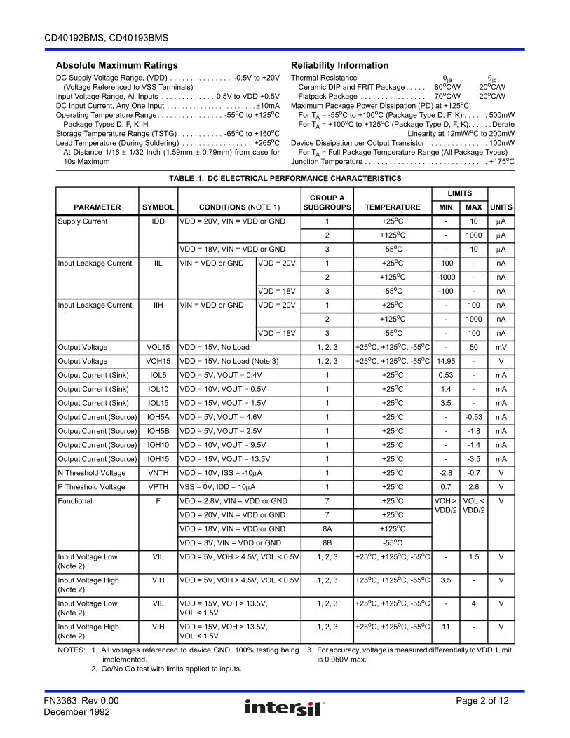
CD40192BMS Presettable BCD Up/Down Counter and theCD40193BMS Presettable Binary Up/Down Counter each con-sist of 4 synchronously clocked, gated “D” type flip-flops con-nected as a counter. The inputs consist of 4 individual jam lines,a PRESET ENABLE control, individual CLOCK UP andCLOCK DOWN signals and a master RESET. Four buffered Qsignal outputs as well as CARRY and BORROW outputs formultiple-stage counting schemes are provided.
The counter is cleared so that all outputs are in a low state by ahigh on the RESET line. A RESET is accomplished asynchro-nously with the clock. Each output is individually programmableasynchronously with the clock to the level on the correspondingjam input when the PRESET ENABLE control is low.
The counter counts up one count on the positive clock edge ofthe CLOCK UP signal provided the CLOCK DOWN line is high.The counter counts down one count on the positive clock edgeof the CLOCK DOWN signal provided the CLOCK UP line ishigh.
The CARRY and BORROW signals are high when the counteris counting up or down. The CARRY signal goes low one-halfclock cycle after the counter reaches its maximum count in thecount-up mode. The BORROW signal goes low one-half clockcycle after the counter reaches its minimum count in the count-down mode. Cascading of multiple packages is easily accom-plished without the need for additional external circuitry by tyingthe BORROW and CARRY outputs to the CLOCK DOWN andCLOCK UP inputs, respectively, of the succeeding counterpackage.
The CD40192BMS and CD40193BMS are supplied in these16-lead outline packages:
Braze Seal DIP *H4W, †H4XFrit Seal DIP H1FCeramic Flatpack *H6P, †H6W* CD40192B Only †CD40193B Only
Features
• CD40192BMS - BCD Type
• CD40193BMS - Binary Type
• High Voltage Type (20V Rating)
• Individual Clock Lines for Counting Up or CountingDown
• Synchronous High-Speed Carry and Borrow Propaga-tion Delays for Cascading
• Asynchronous Reset and Preset Capability
• Medium Speed Operation
- fCL = 8MHz (typ.) at 10V
• 5V, 10V and 15V Parametric Ratings
• Standardize Symmetrical Output Characteristics
• 100% Tested for Quiescent Current at 20V
• Maximum Input Current of 1A at 18V Over Full Pack-age Temperature Range; 100nA at 18V and +25oC
• Noise Margin (Over Full Package/Temperature Range)
- 1V at VDD = 5V
- 2V at VDD = 10V
- 2.5V at VDD = 15V
• Meets All Requirements of JEDEC Tentative StandardNo. 13B, “Standard Specifications for Description of‘B’ Series CMOS Devices”
Applications• Up/Down Difference Counting
• Multistage Ripple Counting
• Synchronous Frequency Dividers
• A/D and D/A Conversion
• Programmable Binary or BCD Counting
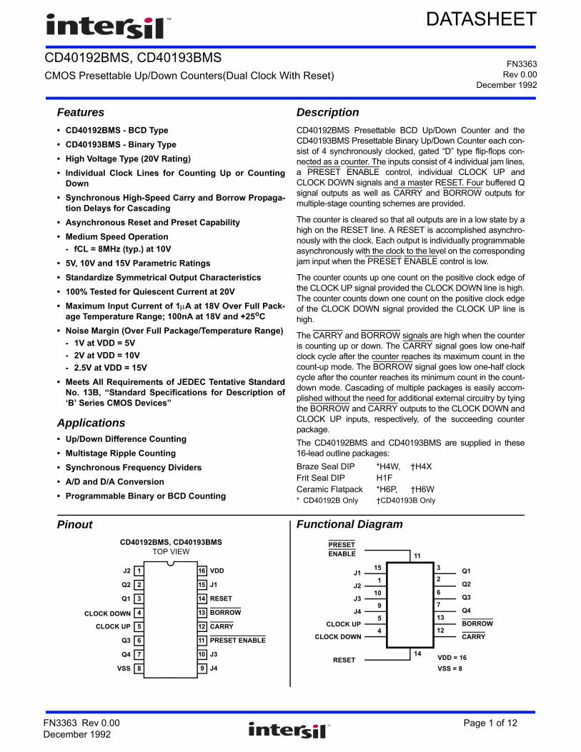
Pinout
CD40192BMS, CD40193BMSTOP VIEW
14
15
16
9
13
12
11
10
1
2
3
4
5
7
6
8
J2
Q2
Q1
CLOCK UP
Q3
VSS
Q4
VDD
RESET
BORROW
CARRY
PRESET ENABLE
J3
J4
J1
CLOCK DOWN
Functional Diagram
3
2
6
7
12
Q1
Q2
Q3
Q4
BORROW
CARRY
15
1
10
9
5
J1
J2
J3
J4
CLOCK UP
CLOCK DOWN
11
14
PRESETENABLE
RESET VDD = 16
VSS = 8
13
4
CD40192BMS, CD40193BMS
Absolute Maximum Ratings Reliability InformationDC Supply Voltage Range, (VDD) . . . . . . . . . . . . . . . -0.5V to +20V
(Voltage Referenced to VSS Terminals)Input Voltage Range, All Inputs . . . . . . . . . . . . .-0.5V to VDD +0.5VDC Input Current, Any One Input 10mAOperating Temperature Range. . . . . . . . . . . . . . . . -55oC to +125oC
Package Types D, F, K, HStorage Temperature Range (TSTG) . . . . . . . . . . . -65oC to +150oCLead Temperature (During Soldering) . . . . . . . . . . . . . . . . . +265oC
At Distance 1/16 1/32 Inch (1.59mm 0.79mm) from case for10s Maximum
Thermal Resistance ja jcCeramic DIP and FRIT Package . . . . . 80oC/W 20oC/WFlatpack Package . . . . . . . . . . . . . . . . 70oC/W 20oC/W
Maximum Package Power Dissipation (PD) at +125oCFor TA = -55oC to +100oC (Package Type D, F, K) . . . . . . 500mWFor TA = +100oC to +125oC (Package Type D, F, K). . . . . . Derate
Linearity at 12mW/oC to 200mWDevice Dissipation per Output Transistor . . . . . . . . . . . . . . . 100mW
For TA = Full Package Temperature Range (All Package Types)Junction Temperature . . . . . . . . . . . . . . . . . . . . . . . . . . . . . . +175oC
TABLE 1. DC ELECTRICAL PERFORMANCE CHARACTERISTICS
PARAMETER SYMBOL CONDITIONS (NOTE 1)GROUP A
SUBGROUPS TEMPERATURE
LIMITS
UNITSMIN MAX
Supply Current IDD VDD = 20V, VIN = VDD or GND 1 +25oC - 10 A
2 +125oC - 1000 A
VDD = 18V, VIN = VDD or GND 3 -55oC - 10 A
Input Leakage Current IIL VIN = VDD or GND VDD = 20V 1 +25oC -100 - nA
2 +125oC -1000 - nA
VDD = 18V 3 -55oC -100 - nA
Input Leakage Current IIH VIN = VDD or GND VDD = 20V 1 +25oC - 100 nA
2 +125oC - 1000 nA
VDD = 18V 3 -55oC - 100 nA
Output Voltage VOL15 VDD = 15V, No Load 1, 2, 3 +25oC, +125oC, -55oC - 50 mV
Output Voltage VOH15 VDD = 15V, No Load (Note 3) 1, 2, 3 +25oC, +125oC, -55oC 14.95 - V
Output Current (Sink) IOL5 VDD = 5V, VOUT = 0.4V 1 +25oC 0.53 - mA
Output Current (Sink) IOL10 VDD = 10V, VOUT = 0.5V 1 +25oC 1.4 - mA
Output Current (Sink) IOL15 VDD = 15V, VOUT = 1.5V 1 +25oC 3.5 - mA
Output Current (Source) IOH5A VDD = 5V, VOUT = 4.6V 1 +25oC - -0.53 mA
Output Current (Source) IOH5B VDD = 5V, VOUT = 2.5V 1 +25oC - -1.8 mA
Output Current (Source) IOH10 VDD = 10V, VOUT = 9.5V 1 +25oC - -1.4 mA
Output Current (Source) IOH15 VDD = 15V, VOUT = 13.5V 1 +25oC - -3.5 mA
N Threshold Voltage VNTH VDD = 10V, ISS = -10A 1 +25oC -2.8 -0.7 V
P Threshold Voltage VPTH VSS = 0V, IDD = 10A 1 +25oC 0.7 2.8 V
Functional F VDD = 2.8V, VIN = VDD or GND 7 +25oC VOH > VDD/2
VOL < VDD/2
V
VDD = 20V, VIN = VDD or GND 7 +25oC
VDD = 18V, VIN = VDD or GND 8A +125oC
VDD = 3V, VIN = VDD or GND 8B -55oC
Input Voltage Low(Note 2)
VIL VDD = 5V, VOH > 4.5V, VOL < 0.5V 1, 2, 3 +25oC, +125oC, -55oC - 1.5 V
Input Voltage High(Note 2)
VIH VDD = 5V, VOH > 4.5V, VOL < 0.5V 1, 2, 3 +25oC, +125oC, -55oC 3.5 - V
Input Voltage Low(Note 2)
VIL VDD = 15V, VOH > 13.5V,VOL < 1.5V
1, 2, 3 +25oC, +125oC, -55oC - 4 V
Input Voltage High(Note 2)
VIH VDD = 15V, VOH > 13.5V,VOL < 1.5V
1, 2, 3 +25oC, +125oC, -55oC 11 - V
NOTES: 1. All voltages referenced to device GND, 100% testing beingimplemented.
2. Go/No Go test with limits applied to inputs.
3. For accuracy, voltage is measured differentially to VDD. Limit is 0.050V max.
FN3363 Rev 0.00 Page 2 of 12December 1992
CD40192BMS, CD40193BMS
TABLE 2. AC ELECTRICAL PERFORMANCE CHARACTERISTICS
PARAMETER SYMBOL CONDITIONS (NOTES 1, 2)GROUP A
SUBGROUPS TEMPERATURE
LIMITS
UNITSMIN MAX
Propagation DelayClock Up or Clock Down to Q
TPHL1TPLH1
VDD = 5V, VIN = VDD or GND 9 +25oC - 500 ns
10, 11 +125oC, -55oC - 675 ns
Propagation DelayReset to Q
TPHL2 VDD = 5V, VIN = VDD or GND 9 +25oC - 500 ns
10, 11 +125oC, -55oC - 675 ns
Propagation DelayPE to Q
TPHL3TPLH3
VDD = 5V, VIN = VDD or GND 9 +25oC - 400 ns
10, 11 +125oC, -55oC - 540 ns
Propagation DelayClock Up to Carry, Clock Down to Borrow
TPHL4TPLH4
VDD = 5V, VIN = VDD or GND 9 +25oC - 320 ns
10, 11 +125oC, -55oC - 432 ns
Propagation Delay PE to Borrow or Carry
TPHL5TPLH5
VDD = 5V, VIN = VDD or GND 9 +25oC - 600 ns
10, 11 +125oC, -55oC - 810 ns
Propagation Delay Reset to Borrow or Carry
TPHL6TPLH6
VDD = 5V, VIN = VDD or GND 9 +25oC - 600 ns
10, 11 +125oC, -55oC - 810 ns
Transition Time TTHLTTLH
VDD = 5V, VIN = VDD or GND 9 +25oC - 200 ns
10, 11 +125oC, -55oC - 270 ns
Maximum Clock Input Frequency
FCL VDD = 5V, VIN = VDD or GND 9 +25oC 2 - MHz
10, 11 +125oC, -55oC 1.48 - MHz
NOTES:
1. CL = 50pF, RL = 200K, Input TR, TF < 20ns.
2. -55oC and +125oC limits guaranteed, 100% testing being implemented.
TABLE 3. ELECTRICAL PERFORMANCE CHARACTERISTICS
PARAMETER SYMBOL CONDITIONS NOTES TEMPERATURE
LIMITS
UNITSMIN MAX
Supply Current IDD VDD = 5V, VIN = VDD or GND 1, 2 -55oC, +25oC - 5 A
+125oC - 150 A
VDD = 10V, VIN = VDD or GND 1, 2 -55oC, +25oC - 10 A
+125oC - 300 A
VDD = 15V, VIN = VDD or GND 1, 2 -55oC, +25oC - 10 A
+125oC - 600 A
Output Voltage VOL VDD = 5V, No Load 1, 2 +25oC, +125oC, -55oC
- 50 mV
Output Voltage VOL VDD = 10V, No Load 1, 2 +25oC, +125oC, -55oC
- 50 mV
Output Voltage VOH VDD = 5V, No Load 1, 2 +25oC, +125oC, -55oC
4.95 - V
Output Voltage VOH VDD = 10V, No Load 1, 2 +25oC, +125oC, -55oC
9.95 - V
Output Current (Sink) IOL5 VDD = 5V, VOUT = 0.4V 1, 2 +125oC 0.36 - mA
-55oC 0.64 - mA
Output Current (Sink) IOL10 VDD = 10V, VOUT = 0.5V 1, 2 +125oC 0.9 - mA
-55oC 1.6 - mA
FN3363 Rev 0.00 Page 3 of 12December 1992

CD40192BMS, CD40193BMS
Output Current (Sink) IOL15 VDD = 15V, VOUT = 1.5V 1, 2 +125oC 2.4 - mA
-55oC 4.2 - mA
Output Current (Source) IOH5A VDD = 5V, VOUT = 4.6V 1, 2 +125oC - -0.36 mA
-55oC - -0.64 mA
Output Current (Source) IOH5B VDD = 5V, VOUT = 2.5V 1, 2 +125oC - -1.15 mA
-55oC - -2.0 mA
Output Current (Source) IOH10 VDD = 10V, VOUT = 9.5V 1, 2 +125oC - -0.9 mA
-55oC - -1.6 mA
Output Current (Source) IOH15 VDD =15V, VOUT = 13.5V 1, 2 +125oC - -2.4 mA
-55oC - -4.2 mA
Input Voltage Low VIL VDD = 10V, VOH > 9V, VOL < 1V 1, 2 +25oC, +125oC, -55oC
- 3 V
Input Voltage High VIH VDD = 10V, VOH > 9V, VOL < 1V 1, 2 +25oC, +125oC, -55oC
7 - V
Propagation DelayClock Up or Down to Q
TPHL1TPLH1
VDD = 10V 1, 2, 3 +25oC - 240 ns
VDD = 15V 1, 2, 3 +25oC - 180 ns
Propagation DelayReset to Q
TPHL2 VDD = 10V 1, 2, 3 +25oC - 240 ns
VDD = 15V 1, 2, 3 +25oC - 180 ns
Propagation DelayPE to Q
TPHL3TPLH3
VDD = 10V 1, 2, 3 +25oC - 200 ns
VDD = 15V 1, 2, 3 +25oC - 140 ns
Propagation DelayClock Up to Carry, Clock Down to Borrow
TPHL4TPLH4
VDD = 10V 1, 2, 3 +25oC - 160 ns
VDD = 15V 1, 2, 3 +25oC - 120 ns
Propagation DelayPE to Borrow or Carry
TPHL5TPLH5
VDD = 10V 1, 2, 3 +25oC - 300 ns
VDD = 15V 1, 2, 3 +25oC - 220 ns
Propagation DelayReset to Borrow or Carry
TPHL6TPLH6
VDD = 10V 1, 2, 3 +25oC - 300 ns
VDD = 15V 1, 2, 3 +25oC - 220 ns
Transition Time TTHL1TTLH1
VDD = 10V 1, 2, 3 +25oC - 100 ns
VDD = 15V 1, 2, 3 +25oC - 80 ns
Maximum Clock Rise and Fall Time
TRCLTFCL
VDD = 5V 1, 2, 3, 4 +25oC - 15 s
VDD = 10V 1, 2, 3, 4 +25oC - 15 s
VDD = 15V 1, 2, 3, 4 +25oC - 5 s
Minimum Removal Time Reset or PE
TREM VDD = 5V 1, 2, 3, 5 +25oC - 80 ns
VDD = 10V 1, 2, 3, 5 +25oC - 40 ns
VDD = 15V 1, 2, 3, 5 +25oC - 30 ns
Minimum Pulse Width Reset
TW VDD = 5V 1, 2, 3 +25oC - 480 ns
VDD = 10V 1, 2, 3 +25oC - 300 ns
VDD = 15V 1, 2, 3 +25oC - 260 ns
Minimum Pulse Width PE TW VDD = 5V 1, 2, 3 +25oC - 240 ns
VDD = 10V 1, 2, 3 +25oC - 170 ns
VDD = 15V 1, 2, 3 +25oC - 140 ns
TABLE 3. ELECTRICAL PERFORMANCE CHARACTERISTICS (Continued)
PARAMETER SYMBOL CONDITIONS NOTES TEMPERATURE
LIMITS
UNITSMIN MAX
FN3363 Rev 0.00 Page 4 of 12December 1992
CD40192BMS, CD40193BMS
Minimum Clock Pulse Width
TW VDD = 5V 1, 2, 3 +25oC - 180 ns
VDD = 10V 1, 2, 3 +25oC - 90 ns
VDD = 15V 1, 2, 3 +25oC - 60 ns
Input Capacitance CIN Reset 1, 2 +25oC - 15 pF
Input Capacitance CIN All Other Inputs 1, 2 +25oC - 7.5 pF
NOTES:
1. All voltages referenced to device GND.
2. The parameters listed on Table 3 are controlled via design or process and are not directly tested. These parameters are characterized on initial design release and upon design changes which would affect these characteristics.
3. CL = 50pF, RL = 200K, Input TR, TF < 20ns.
4. If more than one unit is cascaded, TRCL should be made less than or equal to the sumof the transition time and the fixed propagation delay of the output of the driving stage for the estimated capacitive load.
5. The time required for RESET or PRESET ENABLE control to be removed before clocking. See timing diagram defining TREM.
TABLE 4. POST IRRADIATION ELECTRICAL PERFORMANCE CHARACTERISTICS
PARAMETER SYMBOL CONDITIONS NOTES TEMPERATURE
LIMITS
UNITSMIN MAX
Supply Current IDD VDD = 20V, VIN = VDD or GND 1, 4 +25oC - 25 A
N Threshold Voltage VNTH VDD = 10V, ISS = -10A 1, 4 +25oC -2.8 -0.2 V
N Threshold VoltageDelta
VTN VDD = 10V, ISS = -10A 1, 4 +25oC - 1 V
P Threshold Voltage VTP VSS = 0V, IDD = 10A 1, 4 +25oC 0.2 2.8 V
P Threshold VoltageDelta
VTP VSS = 0V, IDD = 10A 1, 4 +25oC - 1 V
Functional F VDD = 18V, VIN = VDD or GND 1 +25oC VOH > VDD/2
VOL < VDD/2
V
VDD = 3V, VIN = VDD or GND
Propagation Delay Time TPHL TPLH
VDD = 5V 1, 2, 3, 4 +25oC - 1.35 x +25oC Limit
ns
NOTES: 1. All voltages referenced to device GND.
2. CL = 50pF, RL = 200K, Input TR, TF < 20ns.
3. See Table 2 for +25oC limit.
4. Read and Record
TABLE 5. BURN-IN AND LIFE TEST DELTA PARAMETERS +25oC
PARAMETER SYMBOL DELTA LIMIT
Supply Current - MSI-2 IDD 1.0A
Output Current (Sink) IOL5 20% x Pre-Test Reading
Output Current (Source) IOH5A 20% x Pre-Test Reading
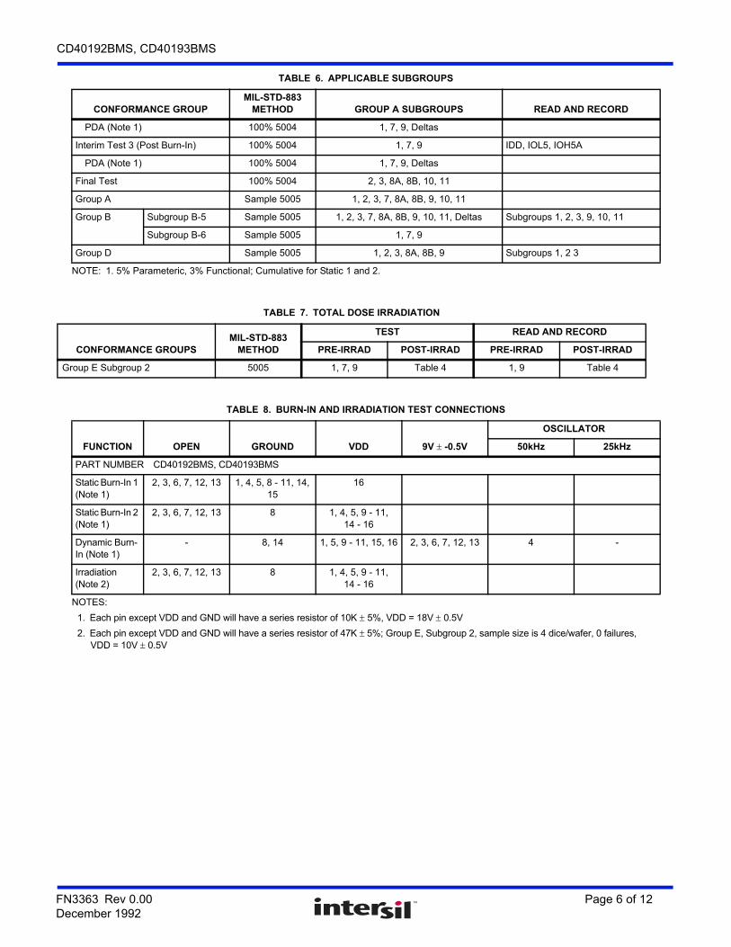
TABLE 6. APPLICABLE SUBGROUPS
CONFORMANCE GROUPMIL-STD-883
METHOD GROUP A SUBGROUPS READ AND RECORD
Initial Test (Pre Burn-In) 100% 5004 1, 7, 9 IDD, IOL5, IOH5A
Interim Test 1 (Post Burn-In) 100% 5004 1, 7, 9 IDD, IOL5, IOH5A
Interim Test 2 (Post Burn-In) 100% 5004 1, 7, 9 IDD, IOL5, IOH5A
TABLE 3. ELECTRICAL PERFORMANCE CHARACTERISTICS (Continued)
PARAMETER SYMBOL CONDITIONS NOTES TEMPERATURE
LIMITS
UNITSMIN MAX
FN3363 Rev 0.00 Page 5 of 12December 1992
CD40192BMS, CD40193BMS
PDA (Note 1) 100% 5004 1, 7, 9, Deltas
Interim Test 3 (Post Burn-In) 100% 5004 1, 7, 9 IDD, IOL5, IOH5A
PDA (Note 1) 100% 5004 1, 7, 9, Deltas
Final Test 100% 5004 2, 3, 8A, 8B, 10, 11
Group A Sample 5005 1, 2, 3, 7, 8A, 8B, 9, 10, 11
Group B Subgroup B-5 Sample 5005 1, 2, 3, 7, 8A, 8B, 9, 10, 11, Deltas Subgroups 1, 2, 3, 9, 10, 11
Subgroup B-6 Sample 5005 1, 7, 9
Group D Sample 5005 1, 2, 3, 8A, 8B, 9 Subgroups 1, 2 3
NOTE: 1. 5% Parameteric, 3% Functional; Cumulative for Static 1 and 2.
TABLE 7. TOTAL DOSE IRRADIATION
CONFORMANCE GROUPSMIL-STD-883
METHOD
TEST READ AND RECORD
PRE-IRRAD POST-IRRAD PRE-IRRAD POST-IRRAD
Group E Subgroup 2 5005 1, 7, 9 Table 4 1, 9 Table 4
TABLE 8. BURN-IN AND IRRADIATION TEST CONNECTIONS
FUNCTION OPEN GROUND VDD 9V -0.5V
OSCILLATOR
50kHz 25kHz
PART NUMBER CD40192BMS, CD40193BMS
Static Burn-In 1 (Note 1)
2, 3, 6, 7, 12, 13 1, 4, 5, 8 - 11, 14, 15
16
Static Burn-In 2 (Note 1)
2, 3, 6, 7, 12, 13 8 1, 4, 5, 9 - 11,14 - 16
Dynamic Burn-In (Note 1)
- 8, 14 1, 5, 9 - 11, 15, 16 2, 3, 6, 7, 12, 13 4 -
Irradiation(Note 2)
2, 3, 6, 7, 12, 13 8 1, 4, 5, 9 - 11,14 - 16
NOTES:
1. Each pin except VDD and GND will have a series resistor of 10K 5%, VDD = 18V 0.5V
2. Each pin except VDD and GND will have a series resistor of 47K 5%; Group E, Subgroup 2, sample size is 4 dice/wafer, 0 failures,VDD = 10V 0.5V
TABLE 6. APPLICABLE SUBGROUPS
CONFORMANCE GROUPMIL-STD-883
METHOD GROUP A SUBGROUPS READ AND RECORD
FN3363 Rev 0.00 Page 6 of 12December 1992
CD40192BMS, CD40193BMS
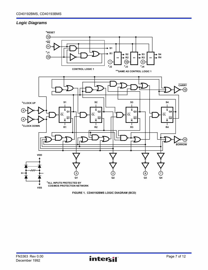
Logic Diagrams
FIGURE 1. CD40192BMS LOGIC DIAGRAM (BCD)
SQ1
Q1
CL
R
S1
R1
15
11
14
1 10 9
** ** **
S1
R1 S2 S3 S4R4R2 R3
*J2 *J3 *J4
*J1
*PE
*RESET
CONTROL LOGIC 1**SAME AS CONTROL LOGIC 1
4
5 SQ2
Q2
CL
R
S2
R2
SQ3
Q3
CL
R
S3
R3
SQ4
Q4
CL
R
S4
R4
12
13
7623
CARRY
BORROW
Q1 Q2 Q3 Q4
*CLOCK UP
*CLOCK DOWN
VDD
VSS
*ALL INPUTS PROTECTED BYCOS/MOS PROTECTION NETWORK
FN3363 Rev 0.00 Page 7 of 12December 1992
CD40192BMS, CD40193BMS
Logic Diagrams (Continued)
FIGURE 2. CD40193BMS LOGIC DIAGRAM (BINARY)
SQ1
Q1
CL
R
S1
R1
15
11
14
1 10 9
** ** **
S1
R1 S2 S3 S4R4R2 R3
*J2 *J3 *J4
*J1
*PE
*RESET
CONTROL LOGIC 1**SAME AS CONTROL LOGIC 1
4
5 SQ2
Q2
CL
R
S2
R2
SQ3
Q3
CL
R
S3
R3
SQ4
Q4
CL
R
S4
R4
12
13
7623
CARRY
BORROW
Q1 Q2 Q3 Q4
*CLOCK UP
*CLOCK DOWN
VDD
VSS
*ALL INPUTS PROTECTED BYCOS/MOS PROTECTION NETWORK
VDD
VDD
VSS
VDD
FN3363 Rev 0.00 Page 8 of 12December 1992

CD40192BMS, CD40193BMS
FIGURE 3. INTERNAL LOGIC OF FLIP-FLOP
Typical Performance Characteristics
SQ
Q
CL
R
CL
R
p
n
CL
CL
CL
CL
p
n
CL
CL
S
p
n
CL
CL
p
n
CL
CL
RQ
Q
=
S
TRUTH TABLE
CLOCK UP CLOCK DOWN PRESET ENABLE RESET ACTION
1 1 0 Count Up
1 1 0 No Count
1 1 0 Count Down
1 1 0 No Count
X X 0 0 Preset
X X X 1 Reset
1 = High Level 0 = Low Level X = Don’t Care
FIGURE 4. TYPICAL OUTPUT LOW (SINK) CURRENTCHARACTERISTICS
FIGURE 5. MIMIMUM OUTPUT LOW (SINK) CURRENT CHARACTERISTICS
10V
5V
AMBIENT TEMPERATURE (TA) = +25oC
GATE-TO-SOURCE VOLTAGE (VGS) = 15V
0 5 10 15
15
10
5
20
25
30
DRAIN-TO-SOURCE VOLTAGE (VDS) (V)
OU
TP
UT
LO
W (S
INK
) CU
RR
EN
T (I
OL
) (m
A)
10V
5V
AMBIENT TEMPERATURE (TA) = +25oC
GATE-TO-SOURCE VOLTAGE (VGS) = 15V
0 5 10 15
7.5
5.0
2.5
10.0
12.5
15.0
DRAIN-TO-SOURCE VOLTAGE (VDS) (V)
OU
TP
UT
LO
W (S
INK
) C
UR
RE
NT
(IO
L) (
mA
)
FN3363 Rev 0.00 Page 9 of 12December 1992
CD40192BMS, CD40193BMS
FIGURE 6. TYPICAL OUTPUT HIGH (SOURCE) CURRENT CHARACTERISTICS
FIGURE 7. MINIMUM OUTPUT HIGH (SOURCE) CURRENTCHARACTERISTICS
FIGURE 8. TYPICAL TRANSITION TIME AS A FUNCTION OF LOAD CAPACITANCE
FIGURE 9. TYPICAL PROPAGATION DELAY TIME AS AFUNCTION OF LOAD CAPACITANCE
FIGURE 10. DYNAMIC POWER DISSIPATION
10V
5V
AMBIENT TEMPERATURE (TA) = +25oC
GATE-TO-SOURCE VOLTAGE (VGS) = 15V
0 5 10 15
7.5
5.0
2.5
10.0
12.5
15.0
DRAIN-TO-SOURCE VOLTAGE (VDS) (V)
OU
TP
UT
LO
W (S
INK
) C
UR
RE
NT
(IO
L) (
mA
)
-10V
-15V
AMBIENT TEMPERATURE (TA) = +25oC0
-5
-10
-15
DRAIN-TO-SOURCE VOLTAGE (VDS) (V)
0-5-10-15
OU
TP
UT
HIG
H (S
OU
RC
E) C
UR
RE
NT
(IO
H)
(mA
)
GATE-TO-SOURCE VOLTAGE (VGS) = -5V
AMBIENT TEMPERATURE (TA) = +25oC
LOAD CAPACITANCE (CL) (pF)0 40 60 80 10020
0
50
100
150
200
SUPPLY VOLTAGE (VDD) = 5V
10V
15V
TR
AN
SIT
ION
TIM
E (
tTH
L,
tTL
H)
(ns
)
AMBIENT TEMPERATURE (TA) = +25oC
LOAD CAPACITANCE (CL) (pF)0 40 60 80 10020
50
100
150
200
SUPPLY VOLTAGE (VDD) = 5V
10V
15V
350
300
250
PR
OP
AG
AT
ION
DE
LA
Y T
IME
(tP
HL
, tP
LH
) (n
s)
400
10 30 50 70 90
8642 8642 2
INPUT FREQUENCY (fIN) (kHz)1 10 102 103 104
864 2 864 2 64
864
2
864
2
864
2
864
2
104
103
102PO
WE
R D
ISS
IPA
TIO
N P
ER
GA
TE
(P
D)
(W
)
AMBIENT TEMPERATURE (TA) = +25oC
CL = 15pF
CL = 50pF
8
105
106
105
FN3363 Rev 0.00 Page 10 of 12December 1992
CD40192BMS, CD40193BMS
FN3363 Rev 0.00 Page 11 of 12December 1992
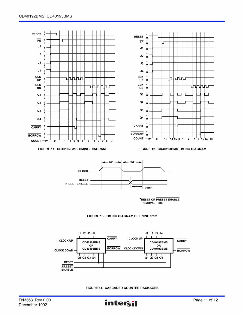
FIGURE 11. CD40192BMS TIMING DIAGRAM FIGURE 12. CD40193BMS TIMING DIAGRAM
FIGURE 13. TIMING DIAGRAM DEFINING trem
FIGURE 14. CASCADED COUNTER PACKAGES
RESET10
10
10
10
10
10
10
10
10
10
10
10
10
10
0 7 8 9 0 1 2 1 0 9 8 7
PE
J1
J2
J3
J4
CLKUP
CLKDN
Q1
Q2
Q3
Q4
CARRY
BORROW
COUNT
RESET101010
10
10
10
10
10
10
10
10
10
10
10
PE
J1
J2
J3
J4
CLKUP
CLKDN
Q1
Q2
Q3
Q4
CARRY
BORROW
COUNT 0 13 14 15 0 1 2 1 0 15 14 13
CLOCK
RESET
PRESET ENABLEtrem*
*RESET OR PRESET ENABLEREMOVAL TIME
tWH tWL
CD40192BMSOR
CD40193BMS
CLOCK UP
CLOCK DOWN
Q1 Q2 Q3 Q4
RESET
PRESETENABLE
J1 J2 J3 J4
CARRY
BORROW
CD40192BMSOR
CD40193BMS
CARRY
Q1 Q2 Q3 Q4
J1 J2 J3 J4
BORROW
CLOCK UP
CLOCK DOWN

FN3363 Rev 0.00 Page 12 of 12December 1992
CD40192BMS, CD40193BMS
Intersil products are manufactured, assembled and tested utilizing ISO9001 quality systems as notedin the quality certifications found at www.intersil.com/en/support/qualandreliability.html
Intersil products are sold by description only. Intersil may modify the circuit design and/or specifications of products at any time without notice, provided that such modification does not, in Intersil's sole judgment, affect the form, fit or function of the product. Accordingly, the reader is cautioned to verify that datasheets are current before placing orders. Information furnished by Intersil is believed to be accurate and reliable. However, no responsibility is assumed by Intersil or its subsidiaries for its use; nor for any infringements of patents or other rights of third parties which may result from its use. No license is granted by implication or otherwise under any patent or patent rights of Intersil or its subsidiaries.
For information regarding Intersil Corporation and its products, see www.intersil.com
For additional products, see www.intersil.com/en/products.html
© Copyright Intersil Americas LLC 1999. All Rights Reserved.All trademarks and registered trademarks are the property of their respective owners.
Chip Dimensions and Pad Layout
METALLIZATION: Thickness: 11kÅ 14kÅ, AL.PASSIVATION: 10.4kÅ - 15.6kÅ, Silane
BOND PADS: 0.004 inches X 0.004 inches MIN
DIE THICKNESS: 0.0198 inches - 0.0218 inches
Dimensions in parentheses are in millimetersand are derived from the basic inch dimensionsas indicated. Grid graduations are in mils (10-3 inch)
Dimensions and pad layout for the CD40192BMSH(dimensions and pad layout for the CD40193BMSHare identical).


![PVCPR11 Edital 3.5 GHz v03.ppt [Modo de Compatibilidade]...2011/06/09 · 35 MHz 35 MHz 10 MHz 10 MHz 10 MHz 10 MHz 10 MHz 10 MHz 3.400,00 MHz 3.600,00 MHz 10 MHz 35 MHz 10 MHz 10](https://cdn.vdocuments.site/doc/165x107/5f7286506e7f433bb4685297/pvcpr11-edital-35-ghz-v03ppt-modo-de-compatibilidade-20110609-35-mhz.jpg)
