Download - AS7030B: User Guide (English)


Document Feedback AS7030B Content Guide
Demo Kit Manual • PUBLIC UG000493 • v1-00 • 2020-Jun-25 63 │ 2
Content Guide
1 Introduction .................................... 3
1.1 Kit Content .................................................... 3 1.2 Ordering Information .................................... 4
2 Getting Started ............................... 5
3 Hardware Description .................... 7
3.1 Hardware Architecture ................................. 7 3.2 Power Supply ............................................... 8
4 AS7030B Overview ........................ 9
4.1 Optical Front End (OFE) .............................. 9 4.2 ECG Amplifier ............................................. 12 4.3 Electrical Analog Front End (EAFE) ........... 14 4.4 Light-to-Frequency Converter (LTF) .......... 15
4.5 ADC and FIFO ........................................... 15 4.6 Digital Interface .......................................... 17 4.7 Sampling Sequencer .................................. 17
5 Software Description ................... 23
5.1 Software Architecture ................................. 23 5.2 Graphical User Interface ............................ 27 5.3 FW, Driver, API .......................................... 55
6 Revision Information ................... 62
7 Legal Information ........................ 63
Document Feedback AS7030B Introduction
Demo Kit Manual • PUBLIC UG000493 • v1-00 • 2020-Jun-25 63 │ 3
1 Introduction
The AS7030B Evaluation Kit allows evaluation of all functions on the AS7030B Biosensor and test
them in various applications.
The initial Evaluation Kit works with USB connection to the PC and comes with a GUI, which enables
the user to change AS7030B register settings, see measurement results and many more.
The SDK (Software Development Kit) currently contains algorithms for HRM, HRV and BP and is
supplied with the Evaluation Kit. The compiled firmware can be flashed onto the STM32 ARM Cortex-
M4 low power MCU.
1.1 Kit Content
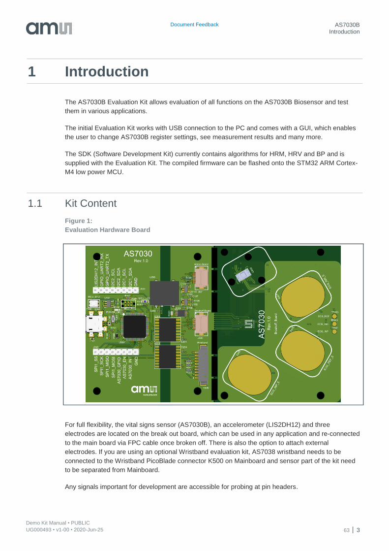
Figure 1:
Evaluation Hardware Board
For full flexibility, the vital signs sensor (AS7030B), an accelerometer (LIS2DH12) and three
electrodes are located on the break out board, which can be used in any application and re-connected
to the main board via FPC cable once broken off. There is also the option to attach external
electrodes. If you are using an optional Wristband evaluation kit, AS7038 wristband needs to be
connected to the Wristband PicoBlade connector K500 on Mainboard and sensor part of the kit need
to be separated from Mainboard.
Any signals important for development are accessible for probing at pin headers.
Document Feedback AS7030B Introduction
Demo Kit Manual • PUBLIC UG000493 • v1-00 • 2020-Jun-25 63 │ 4
1.2 Ordering Information
Ordering Code Description
AS7030B-EVALKIT Evaluation Kit for AS7030B
AS7030B-WRISTBAND Wristband to connect to AS7030B Evalkit
Document Feedback AS7030B Getting Started
Demo Kit Manual • PUBLIC UG000493 • v1-00 • 2020-Jun-25 63 │ 5
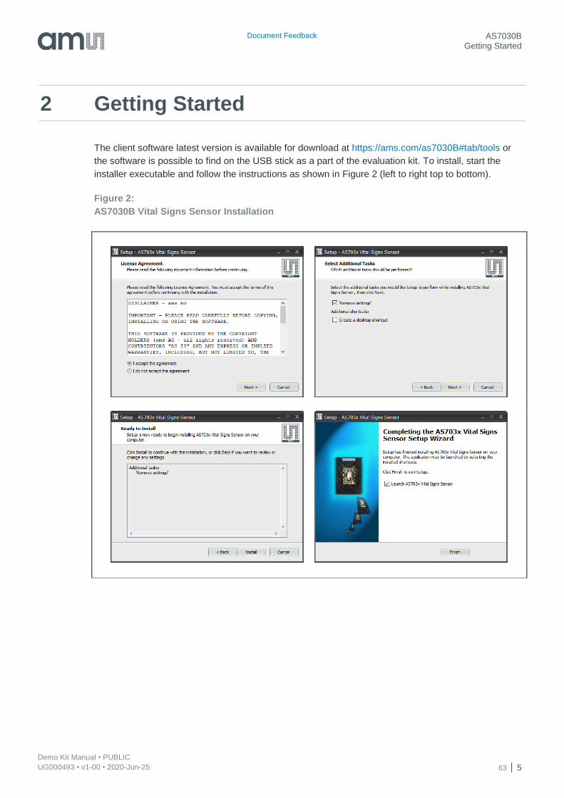
2 Getting Started
The client software latest version is available for download at https://ams.com/as7030B#tab/tools or
the software is possible to find on the USB stick as a part of the evaluation kit. To install, start the
installer executable and follow the instructions as shown in Figure 2 (left to right top to bottom).
Figure 2:
AS7030B Vital Signs Sensor Installation
Document Feedback AS7030B Getting Started
Demo Kit Manual • PUBLIC UG000493 • v1-00 • 2020-Jun-25 63 │ 6
For Windows OS versions prior to Windows® 10, the STSW-STM32102 virtual COM port driver needs
to be installed as well. The driver can be found in the <drivers\STM32_vcp_driver> folder contained
within the client software installation path. To install it, go to your OS version directory (Win7 or Win8,
OS versions prior to Windows® 7 are compatible with the Windows® 7), then:
1. Double click on dpinst_x86.exe if you are running a 32-bits OS version
2. Double click on dpinst_amd64.exe if you are running a 64-bits OS version
3. Follow the instructions
For updating the FW on the evaluation board over USB, the DfuSe driver from STMicroelectronics has
to be installed. This is available in the <drivers\DFU> folder contained within the client software
installation path. To install it, go to your OS version directory (Win7, Win8 or Win8.1), then:
1. Go to [x86] directory or [x64] directory based on your OS version:
2. Double click on dpinst_x86.exe if you are running a 32-bits OS version
3. Double click on dpinst_amd64.exe if you are running a 64-bits OS version
4. Follow the instructions
Information
In some cases, it can be necessary that the driver needs to be installed even on a Windows 10
system. In this case chose the driver installer from the Win 8.1 folder and install.
Document Feedback AS7030B Hardware Description
Demo Kit Manual • PUBLIC UG000493 • v1-00 • 2020-Jun-25 63 │ 7
3 Hardware Description
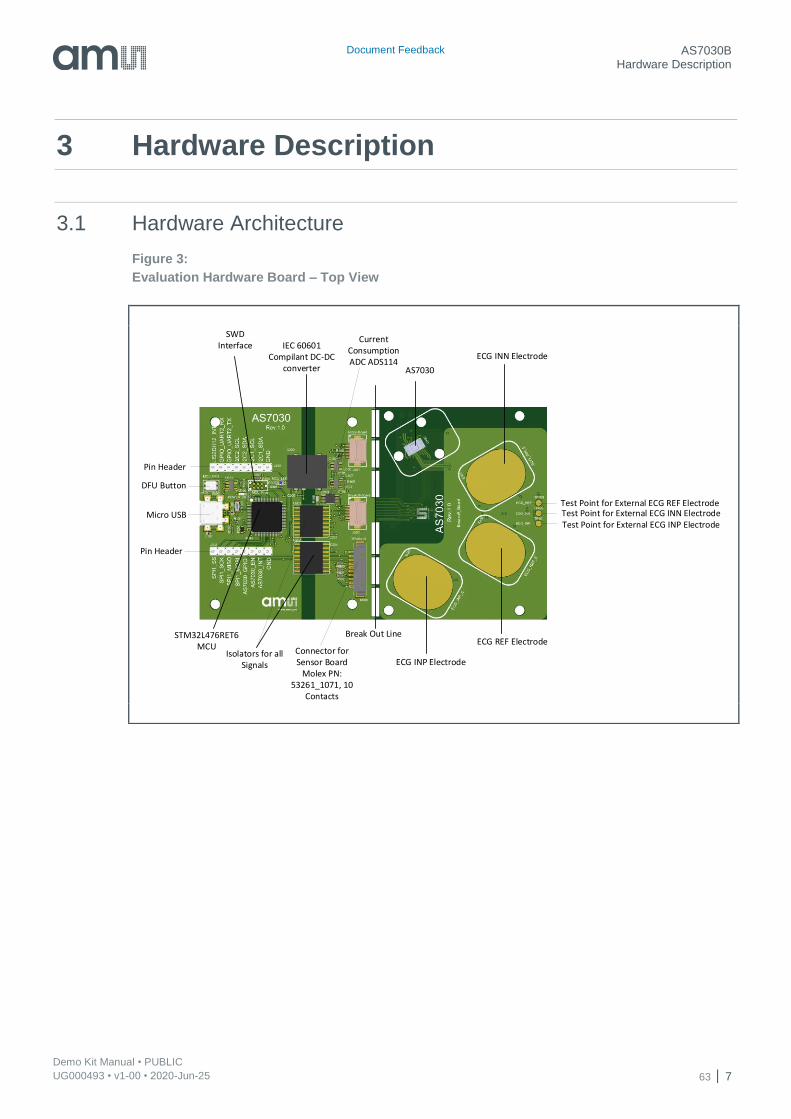
3.1 Hardware Architecture
Figure 3:
Evaluation Hardware Board – Top View
SWD Interface IEC 60601
Compilant DC-DC converter AS7030
ECG INN Electrode
ECG REF Electrode
ECG INP Electrode
Break Out Line
Test Point for External ECG REF ElectrodeTest Point for External ECG INN ElectrodeTest Point for External ECG INP Electrode
STM32L476RET6 MCU
Isolators for all Signals
Pin Header
DFU Button
Micro USB
Pin Header
Current Consumption ADC ADS114
Connector for Sensor Board
Molex PN: 53261_1071, 10
Contacts

Document Feedback AS7030B Hardware Description
Demo Kit Manual • PUBLIC UG000493 • v1-00 • 2020-Jun-25 63 │ 8
Figure 4:
Evaluation Hardware Board – Bottom View
3.2 Power Supply
The AS7030B Eval Kit is supplied by the USB connection. In order to avoid a direct connection from
the electrodes to the power grid, an IEC 60601-1 compliant RECOM DCDC converter (R0.25S-0505/H
or R0.25S-0505/HP) is assembled on the board as well as isolator ICs for all signals passing to the
sensor board. This means that there is no galvanic connection between the sensor board and the
power grid.
Accelerometer LIS2DH12
Connector for External
Electrodes
Connector for Break out Board

Document Feedback AS7030B AS7030B Overview
Demo Kit Manual • PUBLIC UG000493 • v1-00 • 2020-Jun-25 63 │ 9
4 AS7030B Overview
The AS7030B is a photocurrent and voltage sensor capable of taking PPG, ECG, proximity and skin
temperature/resistivity measurements. It integrates an optical front end, ECG amplifier, electrical
analog front end and light to frequency (LTF) converter. It features a built-in sampling sequencer, 128-
byte FIFO, a 14-bit SAR ADC, four GPIO pins and an I2C interface.
4.1 Optical Front End (OFE)
The figure below shows the block diagram of the optical front end.
Figure 5:
Optical Front End
Document Feedback AS7030B AS7030B Overview
Demo Kit Manual • PUBLIC UG000493 • v1-00 • 2020-Jun-25 63 │ 10
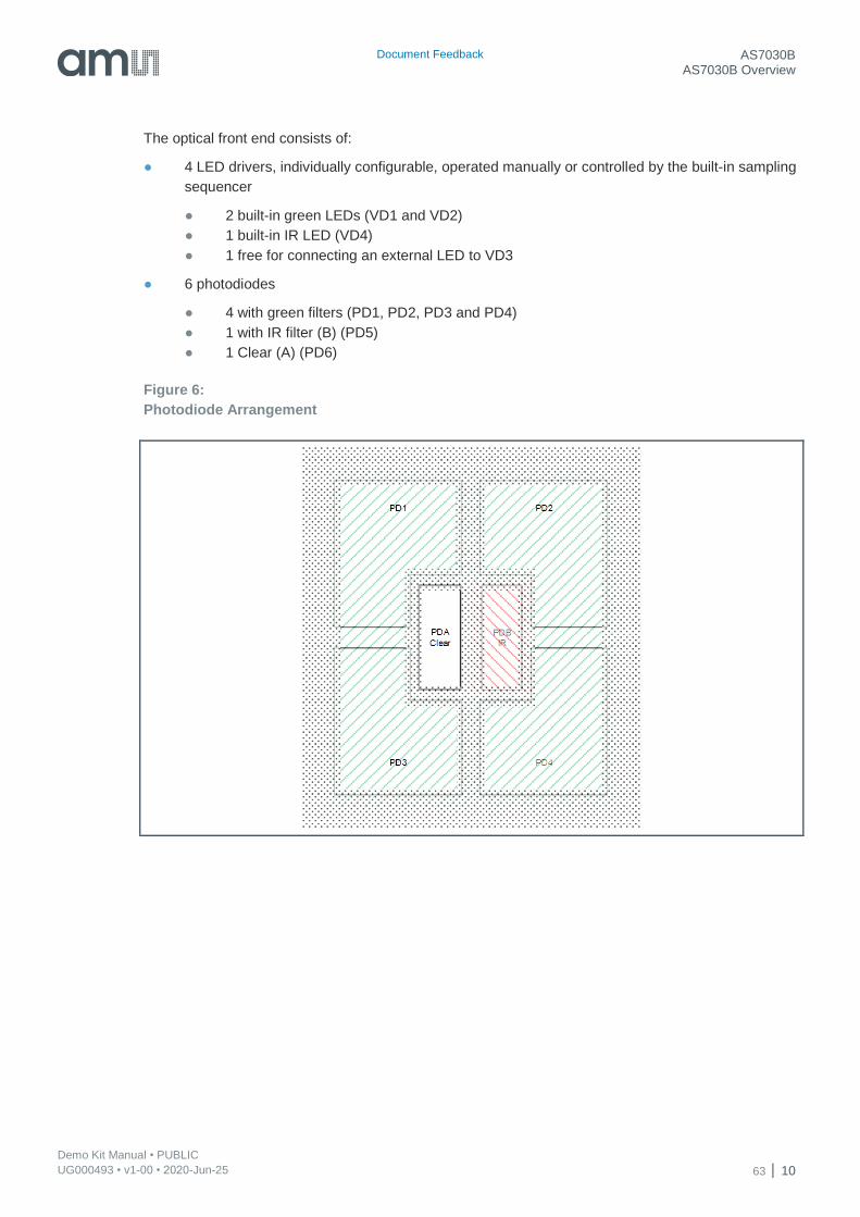
The optical front end consists of:
● 4 LED drivers, individually configurable, operated manually or controlled by the built-in sampling
sequencer
● 2 built-in green LEDs (VD1 and VD2)
● 1 built-in IR LED (VD4)
● 1 free for connecting an external LED to VD3
● 6 photodiodes
● 4 with green filters (PD1, PD2, PD3 and PD4)
● 1 with IR filter (B) (PD5)
● 1 Clear (A) (PD6)
Figure 6:
Photodiode Arrangement
Document Feedback AS7030B AS7030B Overview
Demo Kit Manual • PUBLIC UG000493 • v1-00 • 2020-Jun-25 63 │ 11
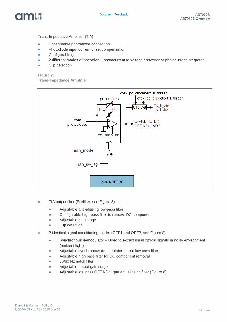
Trans-Impedance Amplifier (TIA)
● Configurable photodiode connection
● Photodiode input current offset compensation
● Configurable gain
● 2 different modes of operation – photocurrent to voltage converter or photocurrent integrator
● Clip detection
Figure 7:
Trans-Impedance Amplifier
● TIA output filter (Prefilter, see Figure 8)
● Adjustable anti-aliasing low-pass filter
● Configurable high-pass filter to remove DC component
● Adjustable gain stage
● Clip detection
● 2 identical signal conditioning blocks (OFE1 and OFE2, see Figure 8)
● Synchronous demodulator – Used to extract small optical signals in noisy environment
(ambient light)
● Adjustable synchronous demodulator output low pass filter
● Adjustable high pass filter for DC component removal
● 50/60 Hz notch filter
● Adjustable output gain stage
● Adjustable low pass OFE1/2 output anti-aliasing filter (Figure 8)

Document Feedback AS7030B AS7030B Overview
Demo Kit Manual • PUBLIC UG000493 • v1-00 • 2020-Jun-25 63 │ 12
Figure 8:
Optical Signal Conditioning
Each of the blocks depicted on Figure 8 can be individually enabled or disabled/bypassed.
4.2 ECG Amplifier
The ECG (electro cardiogram) amplifier is a high impedance, low noise instrumentation amplifier with
analog circuitry to band pass filter the signal. Gain is distributed between 3 gain stages. The gain in
the first stage determines the tradeoff between achievable noise level and achievable input offset
voltage. With the highest gain of 4 at the first gain stage (G1) about 400 mV of offset can be managed.
This value scales up to a max of 1.6 V of offset at gain 1. An optional 50/60 Hz notch filter can be
enabled to attenuate unwanted noise from mains coupling.
The recommended gain settings are 4-6-8 and 4-6-16

Document Feedback AS7030B AS7030B Overview
Demo Kit Manual • PUBLIC UG000493 • v1-00 • 2020-Jun-25 63 │ 13
Figure 9:
ECG Amplifier Circuit
Figure 10:
Recommended ECG Frontend Filter
to electrical frontend
Leads offdetect
ecg_ref_en
SIGREF
ecg_low_leakage_en for diode leakage reduction on ECG_INP and ECG_INN
1 G=1..128
SIGREF
ADC
800Hz
G_ina=18 (programmable 1 .. 48)
Gain StageStage 1Di fferential Ampl i fier
Stage 2High Pass Filter
Filter Gain
1 .. 4 1 .. 12
G2G1
0.33Hz50 Hz 40-200 Hz
Notch Fi l ter
Low PassFi l ter
Anti Al iasingFi l ter
800 Hz
Instrumentational Amplifier
AS7030_ECG_INP
AS7030_ECG_INN
AS7030_ECG_REF
ECG
El
ectr
ode
s
ECG_INPECG_INN
ECG_REF
Document Feedback AS7030B AS7030B Overview
Demo Kit Manual • PUBLIC UG000493 • v1-00 • 2020-Jun-25 63 │ 14
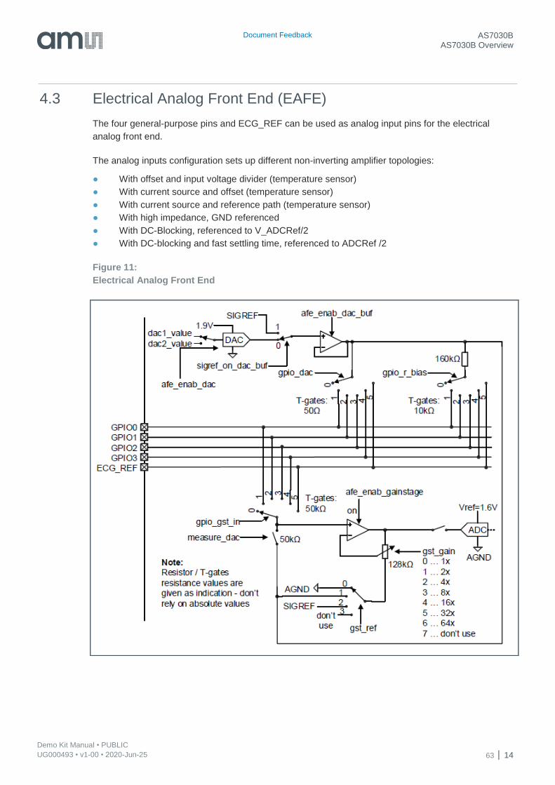
4.3 Electrical Analog Front End (EAFE)
The four general-purpose pins and ECG_REF can be used as analog input pins for the electrical
analog front end.
The analog inputs configuration sets up different non-inverting amplifier topologies:
● With offset and input voltage divider (temperature sensor)
● With current source and offset (temperature sensor)
● With current source and reference path (temperature sensor)
● With high impedance, GND referenced
● With DC-Blocking, referenced to V_ADCRef/2
● With DC-blocking and fast settling time, referenced to ADCRef /2
Figure 11:
Electrical Analog Front End

Document Feedback AS7030B AS7030B Overview
Demo Kit Manual • PUBLIC UG000493 • v1-00 • 2020-Jun-25 63 │ 15
4.4 Light-to-Frequency Converter (LTF)
The LTF module can use any of the photodiodes. Photodiodes connected to the LTF cannot be used
at the same time with TIA. Integration time (itime) is configured in unit steps, one unit step is 3.702 ms.
The unit step can be reduced by 2, 4 or 8, this also reduces the resolution of the conversion. The LTF
modulator can be set to run continuously and write the result of each integration to the FIFO.
Figure 12:
Light-to-Frequency Converter
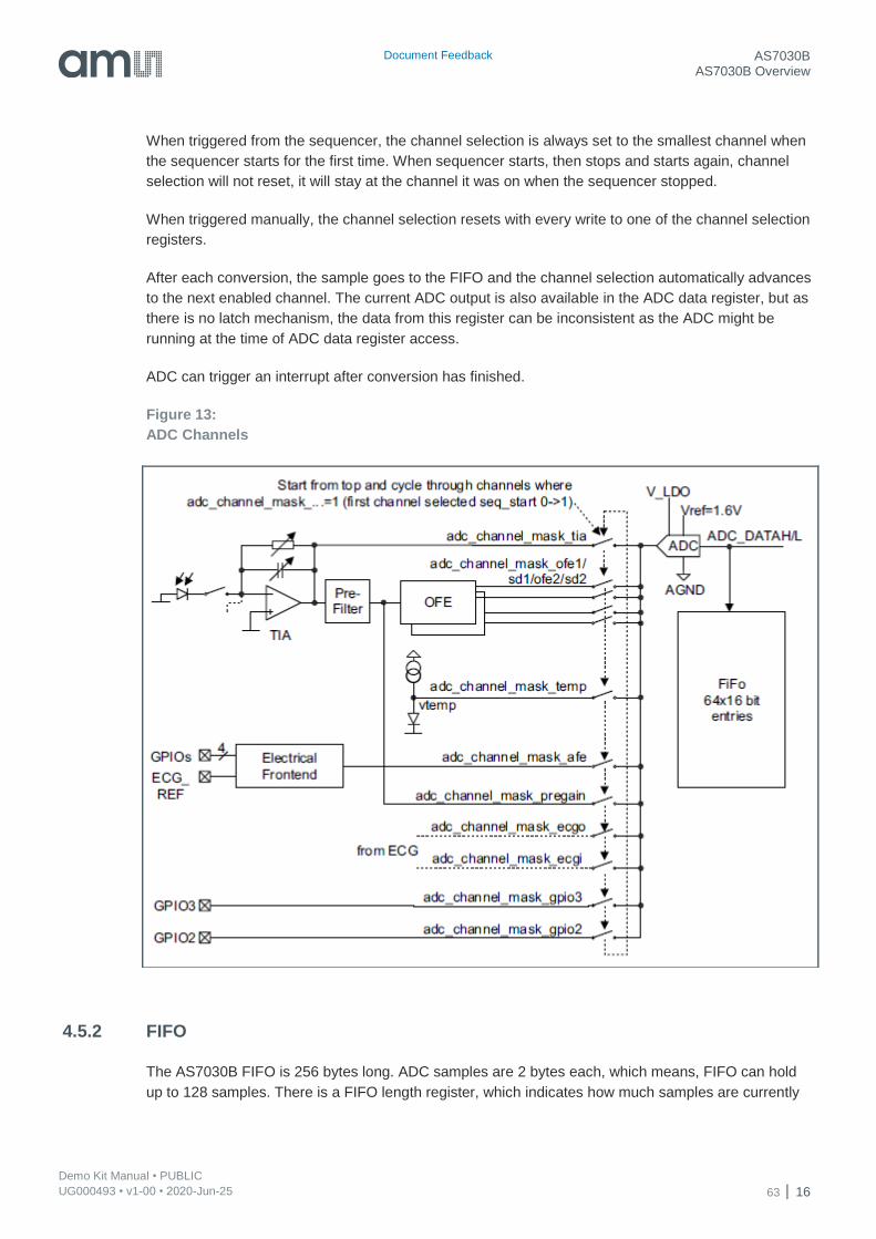
4.5 ADC and FIFO
4.5.1 ADC
The ADC is a 14-bit successive approximation register type with input clock of 1 MHz. A configurable
clock divider can reduce the input clock. One conversion takes 25 clock cycles plus configurable
number of ADC settling clock cycles (64 the default for ADC settling cycles).The ADC can be manually
triggered by register or automatically triggered by the built-in sampling sequencer. Two channel
selection registers ADC_CHANNEL_MASK_L and ADC_CHANNEL_MASK_H define the channels the
ADC will convert. The ADC will start with the channels in ADC_CHANNEL_MASK_L from the LS
asserted bit to the MS asserted bit, then continue with the channels in ADC_CHANNEL_MASK_H
register again from LS asserted bit to MS asserted bit. Then wraps back to the LS bit of
ADC_CHANNEL_MASK_L. Thus, the ADC will go through each channel in the order as shown in
Figure 13 with TIA being the first (smallest index), OFE1 second, SD1 third and so on to the GPIO2
being the last.
Document Feedback AS7030B AS7030B Overview
Demo Kit Manual • PUBLIC UG000493 • v1-00 • 2020-Jun-25 63 │ 16
When triggered from the sequencer, the channel selection is always set to the smallest channel when
the sequencer starts for the first time. When sequencer starts, then stops and starts again, channel
selection will not reset, it will stay at the channel it was on when the sequencer stopped.
When triggered manually, the channel selection resets with every write to one of the channel selection
registers.
After each conversion, the sample goes to the FIFO and the channel selection automatically advances
to the next enabled channel. The current ADC output is also available in the ADC data register, but as
there is no latch mechanism, the data from this register can be inconsistent as the ADC might be
running at the time of ADC data register access.
ADC can trigger an interrupt after conversion has finished.
Figure 13:
ADC Channels
4.5.2 FIFO
The AS7030B FIFO is 256 bytes long. ADC samples are 2 bytes each, which means, FIFO can hold
up to 128 samples. There is a FIFO length register, which indicates how much samples are currently
Document Feedback AS7030B AS7030B Overview
Demo Kit Manual • PUBLIC UG000493 • v1-00 • 2020-Jun-25 63 │ 17
available in the FIFO. The FIFO can send an interrupt when the number of available samples reaches
a certain configurable threshold.
4.6 Digital Interface
4.6.1 GPIO Pins
All four GPIO pins can be digitally controlled and can have pull up/down enabled. They can also be
used as analog input pins for the EAFE, GPIO2 and GPIO3 can additionally be used with the ADC.
4.6.2 Interrupts
An interrupt output pin INT is used to interrupt the host. Depending on the setting in register INTENAB
each of the interrupt source below can assert INT output pin (active low).
● irq_adc: End of ADC conversion
● irq_sequencer: End of sequencer sequence reached.
● irq_ltf: A light-to-frequency conversion is finished.
● irq_adc_threshold: ADC threshold triggered
● irq_fifothreshold: FIFO almost full (as defined in register fifo_threshold)
● irq_fifooverflow: FIFO overflow (error condition, data is lost)
● irq_clipdetect: TIA output and/or SD output exceeded threshold– see details in CLIPSTATUS
● irq_led_supply_low: LED supply low comparator triggered
4.7 Sampling Sequencer
The sampling sequencer synchronizes the LED pulsing, the synchronous demodulator, the ADC and
the integrator times. The sequencer configuration sets the LED on and off times, synchronous
demodulator positive and negative multiplication times, the ADC start time and the integrator start and
stop times. The sequencer generates the 8-bit timings based on the 1 μs input clock. The input clock
can be reduced with a configurable clock divider.
The sequencer executes measurement cycles with a period defined by Equation 1 where SEQ_PER
and SEQ_DIV are registers of AS7030B having values from 0 to 255 (see pages 50 and 51 in the
AS7030B datasheet):
Equation 1:
𝑆𝐸𝑄_𝑃𝐸𝑅 ∗ (𝑆𝐸𝑄_𝐷𝐼𝑉 + 1) ∗ 1𝜇𝑠
SEQ_DIV holds the value of the 1 µs input clock divider.

Document Feedback AS7030B AS7030B Overview
Demo Kit Manual • PUBLIC UG000493 • v1-00 • 2020-Jun-25 63 │ 18
Within one sequencer cycle, the sequencer will:
● Switch on the LEDs at the specified LED start time and then switch them off at the LED stop
time.
● Start the positive and negative synchronous modulator multiplications at the specified start and
stop times for each operation
● Trigger a conversion of the currently selected ADC channel at the time specified by the ADC
start time. After the conversion has finished, ADC channel selection will advance the next
enabled ADC channel, which is measured during the next cycle that gives one ADC channel per
sequencer cycle. For the TIA channel, two additional ADC timings can be specified. That means
TIA can be measured up to 3 times within the same sequencer cycle:
● A 2nd measurement will be done, if the value for “2nd TIA” is specified (> 0) and is greater
than the one given in “1st” plus the time needed for the ADC to finish one conversion.
● A 3rd measurement will be done, if “3rd TIA” value is specified (> 0) and is greater than the
one given in “2nd TIA” plus the time needed for the ADC to finish one conversion.
● In the case of more than one TIA measurement within the same sequencer cycle, it is
important to make sure that the additional measurements can finish within the time of one
sequencer cycle.

Document Feedback AS7030B AS7030B Overview
Demo Kit Manual • PUBLIC UG000493 • v1-00 • 2020-Jun-25 63 │ 19
Figure 14:
Sequencer Block Diagram
4.7.1 Sampling Rate and Subsampling
Throughout this document, sampling rate refers to the rate at which the sequencer produces samples
of the same ADC channel. This depends on the number of enabled ADC channels and on
configuration of the subsampling feature of the sequencer.
Subsampling is used when the application requires lower sample rates than what is possible with the
configured SEQ_PER and SEQ_DIV values, and with the number of enabled ADC channels. Lower
sample rate can also be achieved by setting SEQ_PER and SEQ_DIV to large enough values, but this
is not advisable as SEQ_DIV is multiplied to all the timings of the sequencer, thus the LED pulses will
become very long, which is probably not desired. SEQ_DIV should be kept relatively small for finer
resolution of the times.
Document Feedback AS7030B AS7030B Overview
Demo Kit Manual • PUBLIC UG000493 • v1-00 • 2020-Jun-25 63 │ 20
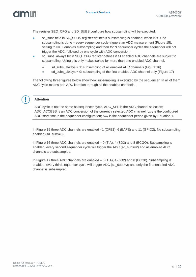
The register SEQ_CFG and SD_SUBS configure how subsampling will be executed:
● sd_subs field in SD_SUBS register defines if subsampling is enabled; when it is 0, no
subsampling is done – every sequencer cycle triggers an ADC measurement (Figure 15);
setting to N>0, enables subsampling and then for N sequencer cycles the sequencer will not
trigger the ADC, followed by one cycle with ADC conversion.
● sd_subs_always bit in SEQ_CFG register defines if all enabled ADC channels are subject to
subsampling. Using this only makes sense for more than one enabled ADC channel.
● sd_subs_always = 1: subsampling of all enabled ADC channels (Figure 16)
● sd_subs_always = 0: subsampling of the first enabled ADC channel only (Figure 17)
The following three figures below show how subsampling is executed by the sequencer. In all of them
ADC cycle means one ADC iteration through all the enabled channels.
Attention
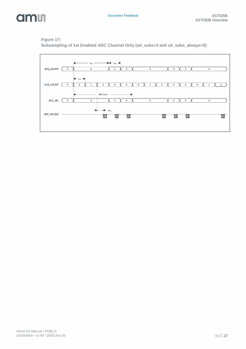
ADC cycle is not the same as sequencer cycle. ADC_SEL is the ADC channel selection;
ADC_ACCESS is an ADC conversion of the currently selected ADC channel; tADC is the configured
ADC start time in the sequencer configuration; tSUB is the sequencer period given by Equation 1.
In Figure 15 three ADC channels are enabled - 1 (OFE1), 6 (EAFE) and 11 (GPIO2). No subsampling
enabled (sd_subs=0).
In Figure 16 three ADC channels are enabled – 0 (TIA), 4 (SD2) and 8 (ECGO). Subsampling is
enabled, every second sequencer cycle will trigger the ADC (sd_subs=2) and all enabled ADC
channels are subsampled.
In Figure 17 three ADC channels are enabled – 0 (TIA), 4 (SD2) and 8 (ECG0). Subsampling is
enabled, every third sequencer cycle will trigger ADC (sd_subs=3) and only the first enabled ADC
channel is subsampled.
Document Feedback AS7030B AS7030B Overview
Demo Kit Manual • PUBLIC UG000493 • v1-00 • 2020-Jun-25 63 │ 21
Figure 15:
No Subsampling (sd_subs=0)
Figure 16:
Subsampling of All Enabled ADC Channels (sd_subs=2 and sd_subs_always=1)
Document Feedback AS7030B AS7030B Overview
Demo Kit Manual • PUBLIC UG000493 • v1-00 • 2020-Jun-25 63 │ 22
Figure 17:
Subsampling of 1st Enabled ADC Channel Only (sd_subs=3 and sd_subs_always=0)
Document Feedback AS7030B Software Description
Demo Kit Manual • PUBLIC UG000493 • v1-00 • 2020-Jun-25 63 │ 23
5 Software Description
5.1 Software Architecture
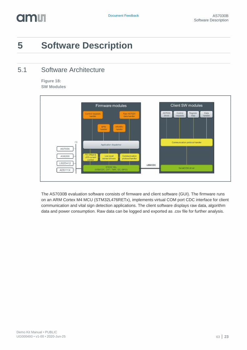
Figure 18:
SW Modules
The AS7030B evaluation software consists of firmware and client software (GUI). The firmware runs
on an ARM Cortex M4 MCU (STM32L476RETx), implements virtual COM port CDC interface for client
communication and vital sign detection applications. The client software displays raw data, algorithm
data and power consumption. Raw data can be logged and exported as .csv file for further analysis.
Document Feedback AS7030B Software Description
Demo Kit Manual • PUBLIC UG000493 • v1-00 • 2020-Jun-25 63 │ 24
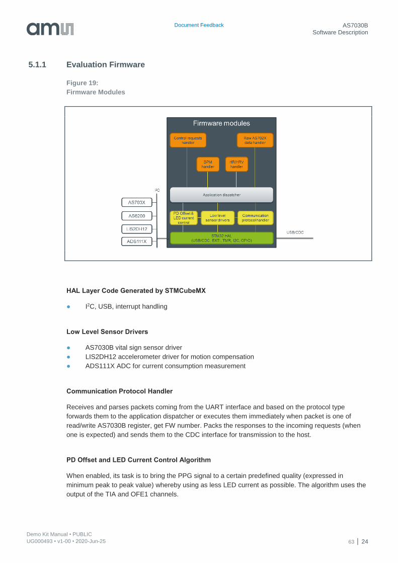
5.1.1 Evaluation Firmware
Figure 19:
Firmware Modules
HAL Layer Code Generated by STMCubeMX
● I2C, USB, interrupt handling
Low Level Sensor Drivers
● AS7030B vital sign sensor driver
● LIS2DH12 accelerometer driver for motion compensation
● ADS111X ADC for current consumption measurement
Communication Protocol Handler
Receives and parses packets coming from the UART interface and based on the protocol type
forwards them to the application dispatcher or executes them immediately when packet is one of
read/write AS7030B register, get FW number. Packs the responses to the incoming requests (when
one is expected) and sends them to the CDC interface for transmission to the host.
PD Offset and LED Current Control Algorithm
When enabled, its task is to bring the PPG signal to a certain predefined quality (expressed in
minimum peak to peak value) whereby using as less LED current as possible. The algorithm uses the
output of the TIA and OFE1 channels.
Document Feedback AS7030B Software Description
Demo Kit Manual • PUBLIC UG000493 • v1-00 • 2020-Jun-25 63 │ 25
It will first check if offset compensation needs to be applied by comparing the averaged TIA to a high
and a low threshold (both fixed in FW, not configurable). If the value is below the low threshold, PD
offset is decreased. If it is above the high threshold and if the currently configured PD offset is < 238,
PD offset is increased, otherwise the LED current is decreased.
If the TIA signal is within the range defined by the low and high thresholds, the algorithm will check if
the amplitude of the OFE1 signal is within certain limits defined by configurable minimum and
maximum. In case the calculated OFE amplitude is outside this range, if OFE1 amplitude is below the
defined minimum, LED current is increased; if it is above the maximum, LED current is decreased.
The range within which the LED current is allowed to change is given by configurable minimum and
maximum.
After a change in PD offset and/or LED input current, the algorithm will not do the OFE1 check for a
period of 1500 milliseconds (this is the period of a 40 BPM heartrate). The current minimum and
maximum values of the OFE1 signal are being reset at a configurable interval.
Refer to chapter PD Offset and LED Current Control Configuration for details on how to configure and
use it.
Application Dispatcher
The application dispatcher is responsible for sending the application requests, received from the client
software to the relevant application for execution. The FW implements 3 types of applications – control
requests handler, raw data handler and vital sign algorithm handlers. Implemented vital sign algorithm
handlers are heart rate monitor (HRM), heart rate variability (HRV) and blood pressure monitor (BPM).
Control Requests Handler
Handles FW control requests like application selection, AGC configuration and measurement
start/stop.
Raw AS7030B Data Handler
Collects and stores raw AS7030B sample data in a data buffer and sends the buffered data to the
client upon request.
Vital Sign Application Handlers – HRM, HRV and BP App Handlers
Aggregates data needed by the relevant algorithm, runs the algorithm and handles data requests sent
from the client.
Document Feedback AS7030B Software Description
Demo Kit Manual • PUBLIC UG000493 • v1-00 • 2020-Jun-25 63 │ 26
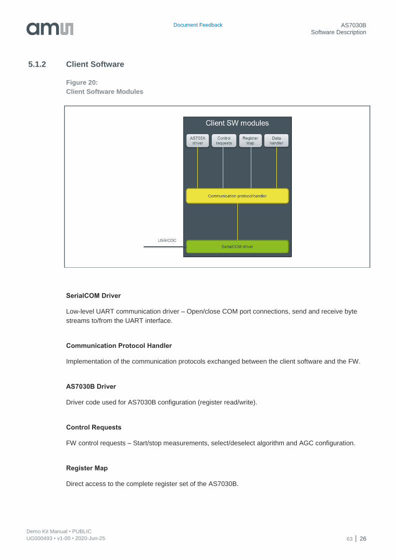
5.1.2 Client Software
Figure 20:
Client Software Modules
SerialCOM Driver
Low-level UART communication driver – Open/close COM port connections, send and receive byte
streams to/from the UART interface.
Communication Protocol Handler
Implementation of the communication protocols exchanged between the client software and the FW.
AS7030B Driver
Driver code used for AS7030B configuration (register read/write).
Control Requests
FW control requests – Start/stop measurements, select/deselect algorithm and AGC configuration.
Register Map
Direct access to the complete register set of the AS7030B.
Document Feedback AS7030B Software Description
Demo Kit Manual • PUBLIC UG000493 • v1-00 • 2020-Jun-25 63 │ 27
Data Handler
Handles incoming data – Updates the relevant ADC channel plot and/or updates vital sign data fields
of the GUI.
5.2 Graphical User Interface
This section describes the Graphical User Interface (GUI) of the AS7030B Vital Sign Sensor
application. The application is designed to be used with AS7030B sensor series evaluation kits.
Information
● User Guide Version - 1.0
● Valid for the following software version - AS703x Vital Sign Sensor v.1.0.16.1
● Supported hardware - AS7030B_Evalboard v1.0
● Download - Navigate to https://ams.com/as7030B#tab/tools and download the latest version.
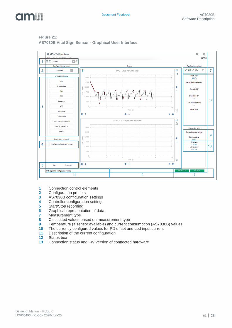
5.2.1 Overview
Figure 21 shows the main window of the graphical user interface. To connect to the board the
connection control elements are used (1). The measured data is displayed in the main section of the
application (6). Additional information about current consumption and temperature is displayed in (9).
Calculated heart rate, calculated blood pressure, heart rate variability are displayed in (8).
Document Feedback AS7030B Software Description
Demo Kit Manual • PUBLIC UG000493 • v1-00 • 2020-Jun-25 63 │ 28
Figure 21:
AS7030B Vital Sign Sensor - Graphical User Interface
1 Connection control elements 2 Configuration presets 3 AS7030B configuration settings 4 Controller configuration settings 5 Start/Stop recording 6 Graphical representation of data 7 Measurement type 8 Calculated values based on measurement type 9 Temperature (if sensor available) and current consumption (AS7030B) values 10 The currently configured values for PD offset and Led input current 11 Description of the current configuration 12 Status box 13 Connection status and FW version of connected hardware
Document Feedback AS7030B Software Description
Demo Kit Manual • PUBLIC UG000493 • v1-00 • 2020-Jun-25 63 │ 29
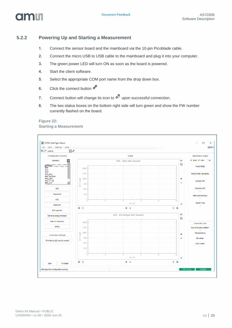
5.2.2 Powering Up and Starting a Measurement
1. Connect the sensor board and the mainboard via the 10-pin Picoblade cable.
2. Connect the micro USB to USB cable to the mainboard and plug it into your computer.
3. The green power LED will turn ON as soon as the board is powered.
4. Start the client software.
5. Select the appropriate COM port name from the drop down box.
6. Click the connect button
7. Connect button will change its icon to upon successful connection.
8. The two status boxes on the bottom right side will turn green and show the FW number
currently flashed on the board.
Figure 22:
Starting a Measurement
Document Feedback AS7030B Software Description
Demo Kit Manual • PUBLIC UG000493 • v1-00 • 2020-Jun-25 63 │ 30
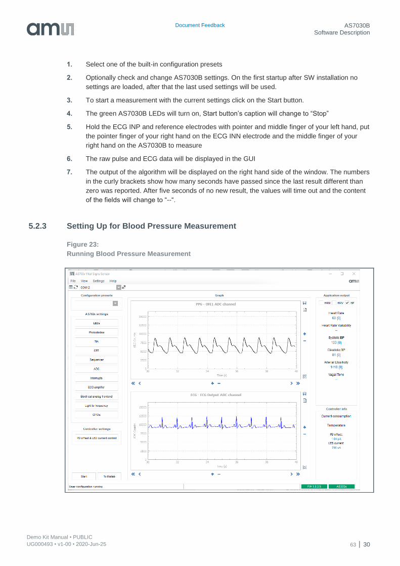
1. Select one of the built-in configuration presets
2. Optionally check and change AS7030B settings. On the first startup after SW installation no
settings are loaded, after that the last used settings will be used.
3. To start a measurement with the current settings click on the Start button.
4. The green AS7030B LEDs will turn on, Start button’s caption will change to “Stop”
5. Hold the ECG INP and reference electrodes with pointer and middle finger of your left hand, put
the pointer finger of your right hand on the ECG INN electrode and the middle finger of your
right hand on the AS7030B to measure
6. The raw pulse and ECG data will be displayed in the GUI
7. The output of the algorithm will be displayed on the right hand side of the window. The numbers
in the curly brackets show how many seconds have passed since the last result different than
zero was reported. After five seconds of no new result, the values will time out and the content
of the fields will change to “--“.
5.2.3 Setting Up for Blood Pressure Measurement
Figure 23:
Running Blood Pressure Measurement

Document Feedback AS7030B Software Description
Demo Kit Manual • PUBLIC UG000493 • v1-00 • 2020-Jun-25 63 │ 31
The blood pressure measurement will give most accurate results with a personalized user profile. A
default user profile is used, if no custom profile exists. To create a new user profile, open menu
Settings and select “Open user data dialog”.
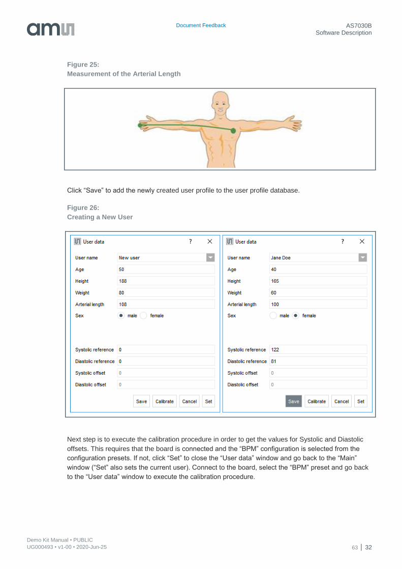
Figure 24:
User Data Window
In the “User data” window click on button “New”. The field “User name” will change to “New user” and
the “New” button will change its caption to “Save”. Enter all field values:
● Age – Age in years
● Height – In cm
● Weight – In kg
● Arterial length – In cm (0 = unknown); to measure the arterial length, please measure the
distance from the tip of your right middle finger to the middle of the line from your left nipple to
the left axle as shown in Figure 25. If the field is left zero, the arterial length will be estimated
based on the user’s height.
● Systolic and Diastolic reference - Obtained with a reference device (e.g. a cuff device)
● Systolic offset - Calculated during calibration, not enabled for user input
● Diastolic offset - Calculated during calibration, not enabled for user input
Document Feedback AS7030B Software Description
Demo Kit Manual • PUBLIC UG000493 • v1-00 • 2020-Jun-25 63 │ 32
Figure 25:
Measurement of the Arterial Length
Click “Save” to add the newly created user profile to the user profile database.
Figure 26:
Creating a New User
Next step is to execute the calibration procedure in order to get the values for Systolic and Diastolic
offsets. This requires that the board is connected and the “BPM” configuration is selected from the
configuration presets. If not, click “Set” to close the “User data” window and go back to the “Main”
window (“Set” also sets the current user). Connect to the board, select the “BPM” preset and go back
to the “User data” window to execute the calibration procedure.

Document Feedback AS7030B Software Description
Demo Kit Manual • PUBLIC UG000493 • v1-00 • 2020-Jun-25 63 │ 33
Calibration Procedure
Select the user to calibrate from the “User name” combo box and click the “Calibrate” button. The
caption of the “Calibrate” button will change to “Calibrating…”.
Figure 27:
User Calibration
Blood pressure measurement will start. The “Start” button will turn to “Stop”, the PPG and ECG graphs
will start plotting the raw data, and blood pressure values will start displaying on the “Main” window.

Document Feedback AS7030B Software Description
Demo Kit Manual • PUBLIC UG000493 • v1-00 • 2020-Jun-25 63 │ 34
Figure 28:
Calibration Ongoing
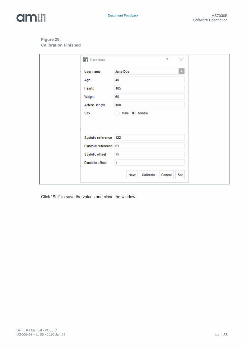
After calculating the five blood pressure values successfully, calibration will be finished, the
measurement is stopped and the values for “Systolic offset” and “Diastolic offset” are updated.
Document Feedback AS7030B Software Description
Demo Kit Manual • PUBLIC UG000493 • v1-00 • 2020-Jun-25 63 │ 35
Figure 29:
Calibration Finished
Click “Set” to save the values and close the window.

Document Feedback AS7030B Software Description
Demo Kit Manual • PUBLIC UG000493 • v1-00 • 2020-Jun-25 63 │ 36
5.2.4 AS7030B Configuration Settings
The AS7030B configuration settings are located on the left of the evaluation software (see Figure 21).
At power-up, the board starts with the following default configuration:
● The two green LEDS - LED1(VD1) and LED2(VD2) are enabled, the LED current set to 1 mA
● Sequencer period set to 2000 µs
● Photodiode Trans-Impedance amplifier (TIA) is on and used
● All filters are on and used
● ADC is set to measure only the optical front end 1 after the gain stage (OFE1)
The individual settings of each of the AS7030B blocks can be viewed/changed in the dedicated
configuration sub menu. To enter the submenus press the corresponding button.
Figure 30:
Submenu Selection
Figure 31:
AS7030B Block Diagram. Highlighted Blocks are Configured in the
According Submenus.
1
2
3
4
5
6
For further information, please refer to the AS7030B Datasheet

Document Feedback AS7030B Software Description
Demo Kit Manual • PUBLIC UG000493 • v1-00 • 2020-Jun-25 63 │ 37
LED Configuration
Attention
LED current, LED mode and LED state can be set in the “LEDs configuration” window. It is
recommended to configure the current only when the output is not active as there is no latch
implemented to keep the 10 bits consistent.
The LED current can be set via sliders in a range of 0.7 -100 mA. Using the Boost option the LED
current can be doubled. The LEDx on option is only active in manual mode. In all other cases the
LEDs will be controlled by the logic.
The textbox LEDs current (mA) shown in Figure 32 allows to enter a numeric value for LED current
which will be set to all LEDs.
Figure 32:
LED Configuration Submenu
Figure 33:
LED Driver Block Diagram
For further information, please refer to the following document:
● AS7030B Datasheet page 24 ff
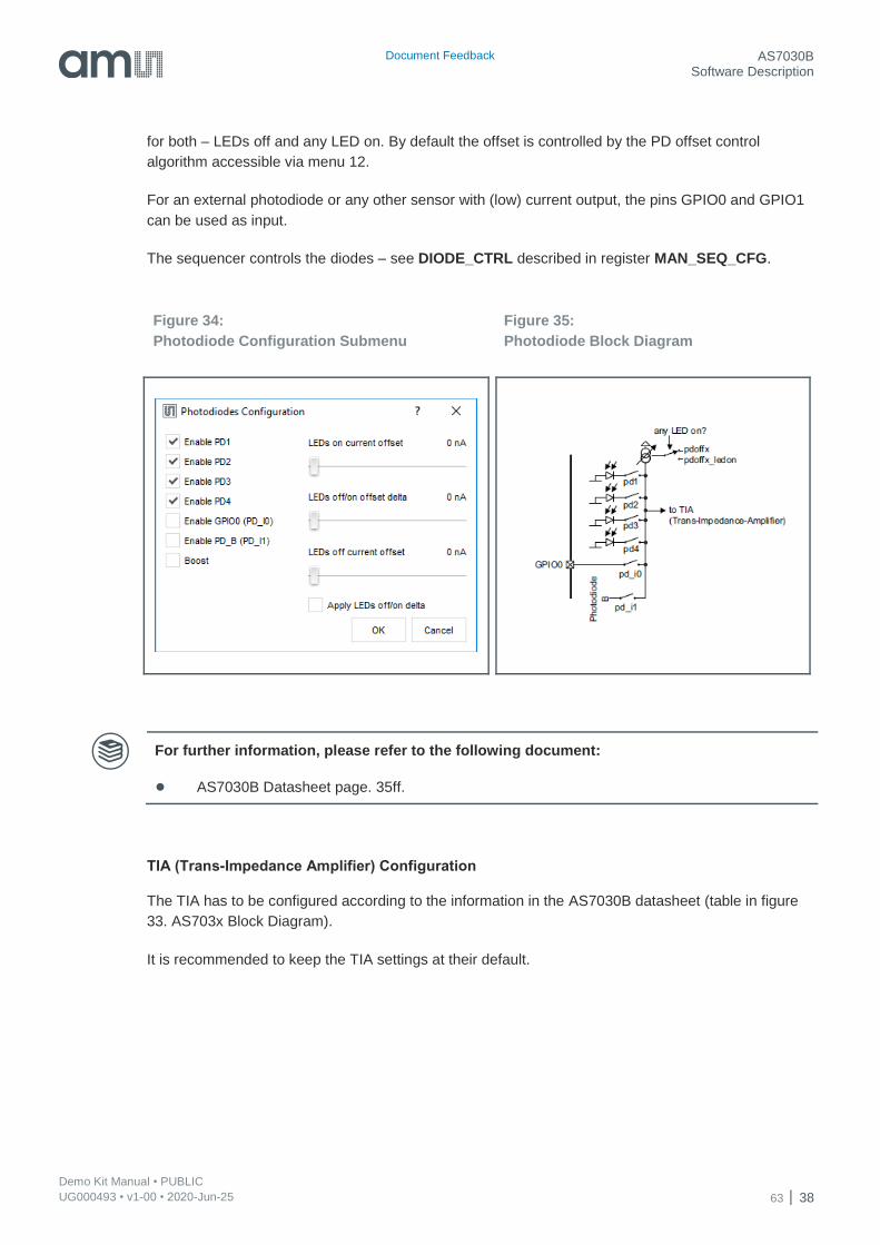
Photodiodes Configuration
Select the photodiodes which are to be connected to TIA input. The offset current is optional, this
allows cancellation of constant light sources like sunlight. Default value for the input offset current is 0
Document Feedback AS7030B Software Description
Demo Kit Manual • PUBLIC UG000493 • v1-00 • 2020-Jun-25 63 │ 38
for both – LEDs off and any LED on. By default the offset is controlled by the PD offset control
algorithm accessible via menu 12.
For an external photodiode or any other sensor with (low) current output, the pins GPIO0 and GPIO1
can be used as input.
The sequencer controls the diodes – see DIODE_CTRL described in register MAN_SEQ_CFG.
Figure 34:
Photodiode Configuration Submenu
Figure 35:
Photodiode Block Diagram
For further information, please refer to the following document:
● AS7030B Datasheet page. 35ff.
TIA (Trans-Impedance Amplifier) Configuration
The TIA has to be configured according to the information in the AS7030B datasheet (table in figure
33. AS703x Block Diagram).
It is recommended to keep the TIA settings at their default.
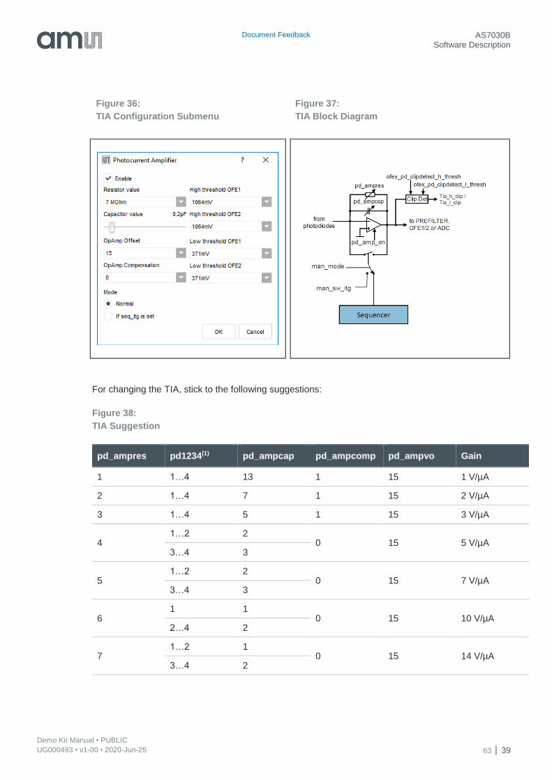
Document Feedback AS7030B Software Description
Demo Kit Manual • PUBLIC UG000493 • v1-00 • 2020-Jun-25 63 │ 39
Figure 36:
TIA Configuration Submenu
Figure 37:
TIA Block Diagram
For changing the TIA, stick to the following suggestions:
Figure 38:
TIA Suggestion
pd_ampres pd1234(1) pd_ampcap pd_ampcomp pd_ampvo Gain
1 1…4 13 1 15 1 V/µA
2 1…4 7 1 15 2 V/µA
3 1…4 5 1 15 3 V/µA
4 1…2 2
0 15 5 V/µA 3…4 3
5 1…2 2
0 15 7 V/µA 3…4 3
6 1 1
0 15 10 V/µA 2…4 2
7 1…2 1
0 15 14 V/µA 3…4 2
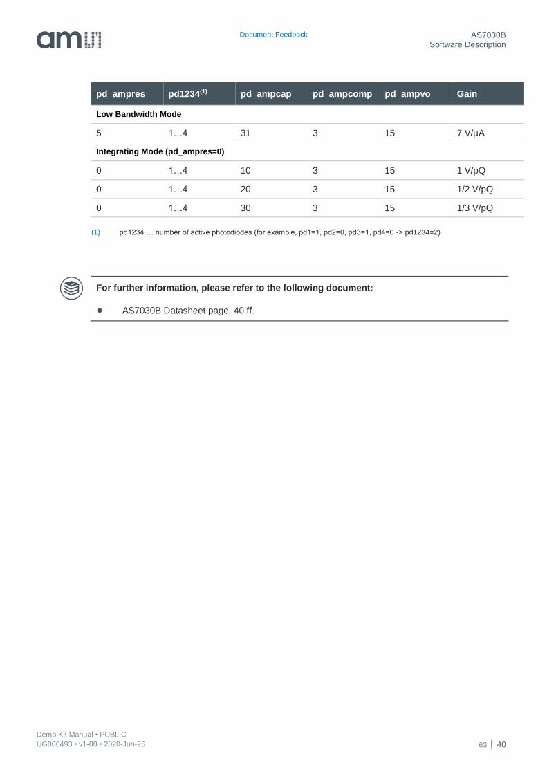
Document Feedback AS7030B Software Description
Demo Kit Manual • PUBLIC UG000493 • v1-00 • 2020-Jun-25 63 │ 40
pd_ampres pd1234(1) pd_ampcap pd_ampcomp pd_ampvo Gain
Low Bandwidth Mode
5 1…4 31 3 15 7 V/µA
Integrating Mode (pd_ampres=0)
0 1…4 10 3 15 1 V/pQ
0 1…4 20 3 15 1/2 V/pQ
0 1…4 30 3 15 1/3 V/pQ
(1) pd1234 … number of active photodiodes (for example, pd1=1, pd2=0, pd3=1, pd4=0 -> pd1234=2)
For further information, please refer to the following document:
● AS7030B Datasheet page. 40 ff.
Document Feedback AS7030B Software Description
Demo Kit Manual • PUBLIC UG000493 • v1-00 • 2020-Jun-25 63 │ 41
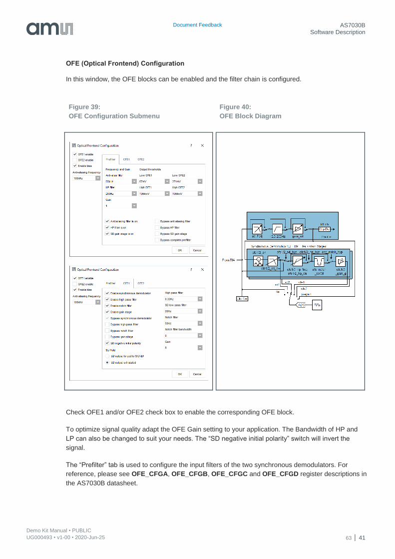
OFE (Optical Frontend) Configuration
In this window, the OFE blocks can be enabled and the filter chain is configured.
Figure 39:
OFE Configuration Submenu
Figure 40:
OFE Block Diagram
Check OFE1 and/or OFE2 check box to enable the corresponding OFE block.
To optimize signal quality adapt the OFE Gain setting to your application. The Bandwidth of HP and
LP can also be changed to suit your needs. The “SD negative initial polarity” switch will invert the
signal.
The “Prefilter” tab is used to configure the input filters of the two synchronous demodulators. For
reference, please see OFE_CFGA, OFE_CFGB, OFE_CFGC and OFE_CFGD register descriptions in
the AS7030B datasheet.
Document Feedback AS7030B Software Description
Demo Kit Manual • PUBLIC UG000493 • v1-00 • 2020-Jun-25 63 │ 42
For further information, please refer to the following document:
● AS7030B Datasheet page. 47 ff …
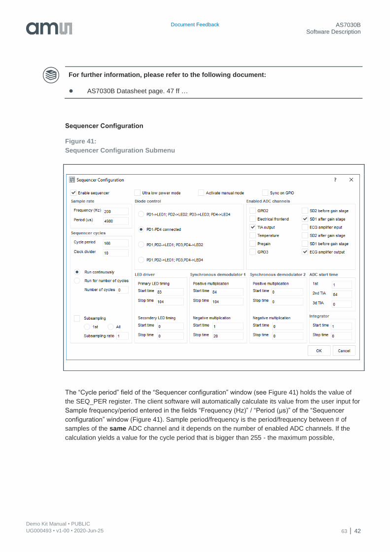
Sequencer Configuration
Figure 41:
Sequencer Configuration Submenu
The “Cycle period” field of the “Sequencer configuration” window (see Figure 41) holds the value of
the SEQ_PER register. The client software will automatically calculate its value from the user input for
Sample frequency/period entered in the fields “Frequency (Hz)” / “Period (µs)” of the “Sequencer
configuration” window (Figure 41). Sample period/frequency is the period/frequency between # of
samples of the same ADC channel and it depends on the number of enabled ADC channels. If the
calculation yields a value for the cycle period that is bigger than 255 - the maximum possible,
Document Feedback AS7030B Software Description
Demo Kit Manual • PUBLIC UG000493 • v1-00 • 2020-Jun-25 63 │ 43
subsampling will be enabled1. Please refer to Sampling Rate and Subsampling for details on sampling
rate.
Use this window to enable/disable ADC channels.
Any change in the values of the fields for sample frequency, sample period, cycle period and in the
ADC channel selection will cause a new calculation of the values for the rest of the fields.
For further information, please refer to the following document:
AS7030B Datasheet page. 47 ff.
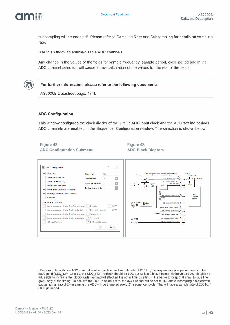
ADC Configuration
This window configures the clock divider of the 1 MHz ADC input clock and the ADC settling periods.
ADC channels are enabled in the Sequencer Configuration window. The selection is shown below.
Figure 42:
ADC Configuration Submenu
Figure 43:
ADC Block Diagram
1 For example, with one ADC channel enabled and desired sample rate of 200 Hz, the sequencer cycle period needs to be 5000 µs. If (SEQ_DIV+1) is 10, the SEQ_PER register should be 500, but as it is 8 bits, it cannot fit the value 500. It is also not advisable to increase the clock divider as that will affect all the other timing settings, it is better to keep that small to give finer granularity of the timing. To achieve the 200 Hz sample rate, the cycle period will be set to 250 and subsampling enabled with subsampling ratio of 2 – meaning the ADC will be triggered every 2nd sequencer cycle. That will give a sample rate of 200 Hz / 5000 µs period.
Document Feedback AS7030B Software Description
Demo Kit Manual • PUBLIC UG000493 • v1-00 • 2020-Jun-25 63 │ 44
For further information, please refer to the following document:
● AS7030B Datasheet page. 98 ff.
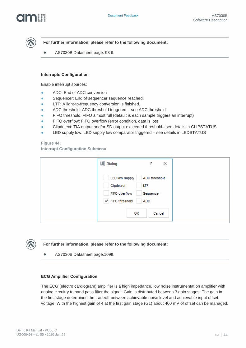
Interrupts Configuration
Enable interrupt sources:
● ADC: End of ADC conversion
● Sequencer: End of sequencer sequence reached.
● LTF: A light-to-frequency conversion is finished.
● ADC threshold: ADC threshold triggered – see ADC threshold.
● FIFO threshold: FIFO almost full (default is each sample triggers an interrupt)
● FIFO overflow: FIFO overflow (error condition, data is lost
● Clipdetect: TIA output and/or SD output exceeded threshold– see details in CLIPSTATUS
● LED supply low: LED supply low comparator triggered – see details in LEDSTATUS
Figure 44:
Interrupt Configuration Submenu
For further information, please refer to the following document:
● AS7030B Datasheet page.109ff.
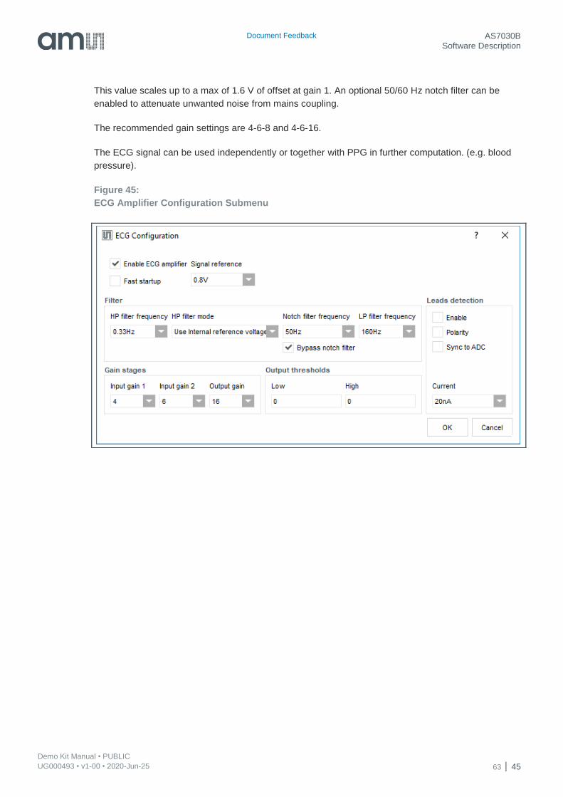
ECG Amplifier Configuration
The ECG (electro cardiogram) amplifier is a high impedance, low noise instrumentation amplifier with
analog circuitry to band pass filter the signal. Gain is distributed between 3 gain stages. The gain in
the first stage determines the tradeoff between achievable noise level and achievable input offset
voltage. With the highest gain of 4 at the first gain stage (G1) about 400 mV of offset can be managed.
Document Feedback AS7030B Software Description
Demo Kit Manual • PUBLIC UG000493 • v1-00 • 2020-Jun-25 63 │ 45
This value scales up to a max of 1.6 V of offset at gain 1. An optional 50/60 Hz notch filter can be
enabled to attenuate unwanted noise from mains coupling.
The recommended gain settings are 4-6-8 and 4-6-16.
The ECG signal can be used independently or together with PPG in further computation. (e.g. blood
pressure).
Figure 45:
ECG Amplifier Configuration Submenu
Document Feedback AS7030B Software Description
Demo Kit Manual • PUBLIC UG000493 • v1-00 • 2020-Jun-25 63 │ 46
Figure 46:
ECG Amplifier Block Diagram
For further information, please refer to the following document:
● AS7030B Datasheet page. 91ff.
to electrical frontend
Leads offdetect
ecg_ref_en
SIGREF
ecg_low_leakage_en for diode leakage reduction on ECG_INP and ECG_INN
1 G=1..128
SIGREF
ADC
800Hz
G_ina=18 (programmable 1 .. 48)
Gain StageStage 1Di fferential Ampl i fier
Stage 2High Pass Filter
Filter Gain
1 .. 4 1 .. 12
G2G1
0.33Hz50 Hz 40-200 Hz
Notch Fi l ter
Low PassFi l ter
Anti Al iasingFi l ter
800 Hz
Instrumentational Amplifier
AS7030_ECG_INP
AS7030_ECG_INN
AS7030_ECG_REF
ECG
E
lect
rod
es
ECG_INPECG_INN
ECG_REF
Document Feedback AS7030B Software Description
Demo Kit Manual • PUBLIC UG000493 • v1-00 • 2020-Jun-25 63 │ 47
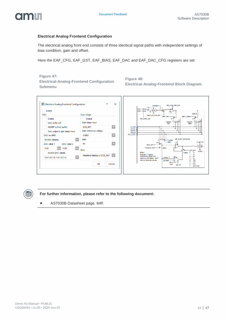
Electrical Analog Frontend Configuration
The electrical analog front end consists of three identical signal paths with independent settings of
bias condition, gain and offset.
Here the EAF_CFG, EAF_GST, EAF_BIAS, EAF_DAC and EAF_DAC_CFG registers are set.
Figure 47:
Electrical-Analog-Frontend Configuration
Submenu
Figure 48:
Electrical-Analog-Frontend Block Diagram
For further information, please refer to the following document:
● AS7030B Datasheet page. 84ff.
Document Feedback AS7030B Software Description
Demo Kit Manual • PUBLIC UG000493 • v1-00 • 2020-Jun-25 63 │ 48
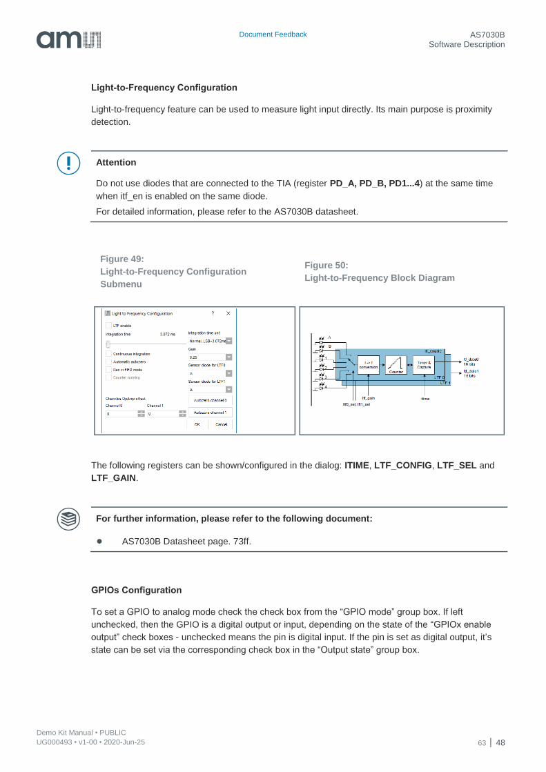
Light-to-Frequency Configuration
Light-to-frequency feature can be used to measure light input directly. Its main purpose is proximity
detection.
Attention
Do not use diodes that are connected to the TIA (register PD_A, PD_B, PD1...4) at the same time
when itf_en is enabled on the same diode.
For detailed information, please refer to the AS7030B datasheet.
The following registers can be shown/configured in the dialog: ITIME, LTF_CONFIG, LTF_SEL and
LTF_GAIN.
For further information, please refer to the following document:
● AS7030B Datasheet page. 73ff.
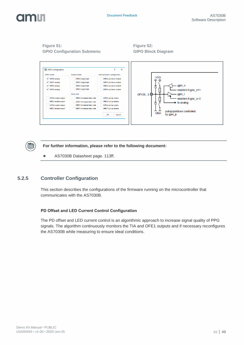
GPIOs Configuration
To set a GPIO to analog mode check the check box from the “GPIO mode” group box. If left
unchecked, then the GPIO is a digital output or input, depending on the state of the “GPIOx enable
output” check boxes - unchecked means the pin is digital input. If the pin is set as digital output, it’s
state can be set via the corresponding check box in the “Output state” group box.
Figure 49:
Light-to-Frequency Configuration
Submenu
Figure 50:
Light-to-Frequency Block Diagram
Document Feedback AS7030B Software Description
Demo Kit Manual • PUBLIC UG000493 • v1-00 • 2020-Jun-25 63 │ 49
Figure 51:
GPIO Configuration Submenu
Figure 52:
GIPO Block Diagram
For further information, please refer to the following document:
● AS7030B Datasheet page. 113ff.
5.2.5 Controller Configuration
This section describes the configurations of the firmware running on the microcontroller that
communicates with the AS7030B.
PD Offset and LED Current Control Configuration
The PD offset and LED current control is an algorithmic approach to increase signal quality of PPG
signals. The algorithm continuously monitors the TIA and OFE1 outputs and if necessary reconfigures
the AS7030B while measuring to ensure ideal conditions.

Document Feedback AS7030B Software Description
Demo Kit Manual • PUBLIC UG000493 • v1-00 • 2020-Jun-25 63 │ 50
Figure 53:
PD Offset & LED Current Control Submenu
Minimum OFE1 signal amplitude – If the amplitude of the OFE1 signal drops below that value, LED
current will be increased, if LED current control is enabled.
Maximum OFE1 signal amplitude – If the amplitude of the OFE1 signal grows above that value, LED
current will be decreased, if LED current control is enabled.
Averaging for TIA offset compensation – How many samples are averaged before TIA mean value is
assessed based on which PD offset is corrected.
OFE1 min and max reset interval – The interval at which the min and max values are calculated over a
moving average are reset in order to keep a recent history and to avoid random spikes.
Minimum and maximum LED output current – Sets the range in which the LED current can move if
LED current control is enabled. If LED current control is disabled the LED have constant LED current
set in the LED Configuration window.
Enable TIA offset compensation and Enable OFE amplitude control – Check boxes define what will be
controlled by the algorithm and if the algorithm is enabled. If both checkboxes are unchecked, the
algorithm is disabled and there will be no correction for TIA offset and LED current control.
Enable TIA offset compensation check box: When checked, enables TIA offset compensation.
Enable OFE amplitude control check box: When checked, enables LED current control. LED current
control only works together with TIA offset compensation.

Document Feedback AS7030B Software Description
Demo Kit Manual • PUBLIC UG000493 • v1-00 • 2020-Jun-25 63 │ 51
5.2.6 Advanced Settings
Additional ADC Channels and Light-to-Frequency Data Display
The AS7030B Vital Sign Sensors evaluation software allows to display multiple channels. The PPG
and ECG channels are always active in the main windows. Additional channels can be displayed via
the View menu as shown in Figure 54
To display a data plot of an ADC channel other than OFE1 and ECG Output, click on menu “View
ADC Channels” and then on the desired ADC channel.
For Light-to-Frequency data output, click on “View LTF”.
A separate plot window will open.
Figure 54:
Additional Output Channels
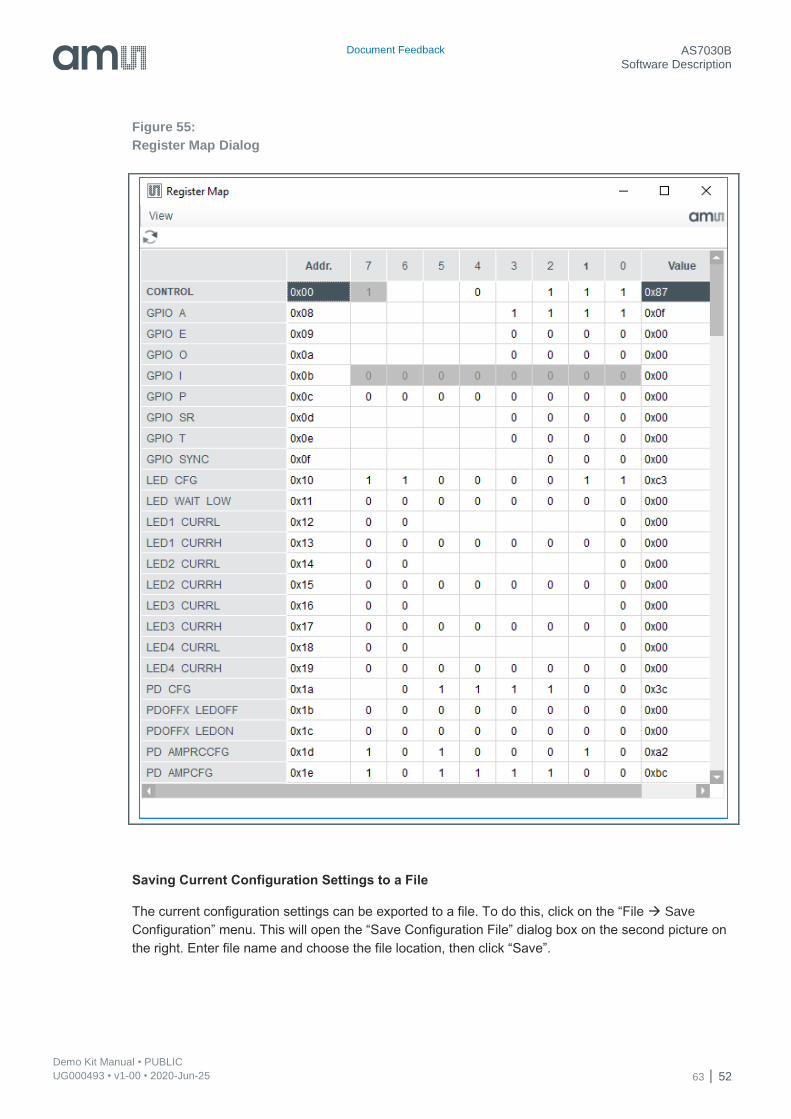
Register Map
The “Register Map” window is used to view/change the contents of the complete set of AS7030B user
register. To open it, click on the “View Register Map” menu.
Changing a register value can be done either by modifying its value in the relevant “Value” field or by
toggling a bit by clicking on the relevant bit cell. Changing a value in the register map will not update
the current selection in the configuration windows of the GUI. Also, a change in any of the
configuration windows will not trigger an automatic update of the already opened register map window.
To update the values, click on the refresh button marked with the orange rounded rectangle on the
“Register Map” picture on the right.
Document Feedback AS7030B Software Description
Demo Kit Manual • PUBLIC UG000493 • v1-00 • 2020-Jun-25 63 │ 52
Figure 55:
Register Map Dialog
Saving Current Configuration Settings to a File
The current configuration settings can be exported to a file. To do this, click on the “File Save
Configuration” menu. This will open the “Save Configuration File” dialog box on the second picture on
the right. Enter file name and choose the file location, then click “Save”.
Document Feedback AS7030B Software Description
Demo Kit Manual • PUBLIC UG000493 • v1-00 • 2020-Jun-25 63 │ 53
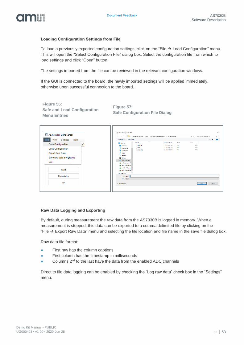
Loading Configuration Settings from File
To load a previously exported configuration settings, click on the “File Load Configuration” menu.
This will open the “Select Configuration File” dialog box. Select the configuration file from which to
load settings and click “Open” button.
The settings imported from the file can be reviewed in the relevant configuration windows.
If the GUI is connected to the board, the newly imported settings will be applied immediately,
otherwise upon successful connection to the board.
Figure 56:
Safe and Load Configuration
Menu Entries
Figure 57:
Safe Configuration File Dialog
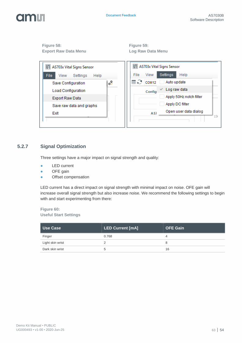
Raw Data Logging and Exporting
By default, during measurement the raw data from the AS7030B is logged in memory. When a
measurement is stopped, this data can be exported to a comma delimited file by clicking on the
“File Export Raw Data” menu and selecting the file location and file name in the save file dialog box.
Raw data file format:
● First raw has the column captions
● First column has the timestamp in milliseconds
● Columns 2nd to the last have the data from the enabled ADC channels
Direct to file data logging can be enabled by checking the “Log raw data” check box in the “Settings”
menu.
Document Feedback AS7030B Software Description
Demo Kit Manual • PUBLIC UG000493 • v1-00 • 2020-Jun-25 63 │ 54
Figure 58:
Export Raw Data Menu
Figure 59:
Log Raw Data Menu
5.2.7 Signal Optimization
Three settings have a major impact on signal strength and quality:
● LED current
● OFE gain
● Offset compensation
LED current has a direct impact on signal strength with minimal impact on noise. OFE gain will
increase overall signal strength but also increase noise. We recommend the following settings to begin
with and start experimenting from there:
Figure 60:
Useful Start Settings
Use Case LED Current [mA] OFE Gain
Finger 0.768 4
Light skin wrist 2 8
Dark skin wrist 5 16
Document Feedback AS7030B Software Description
Demo Kit Manual • PUBLIC UG000493 • v1-00 • 2020-Jun-25 63 │ 55
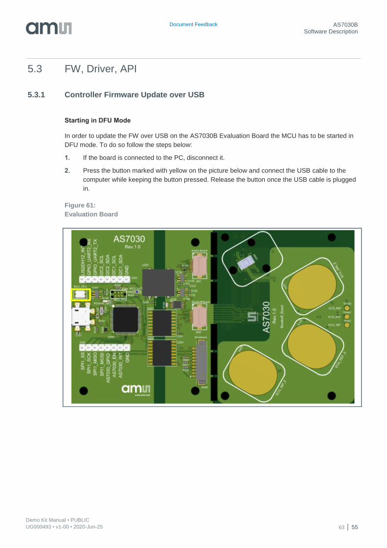
5.3 FW, Driver, API
5.3.1 Controller Firmware Update over USB
Starting in DFU Mode
In order to update the FW over USB on the AS7030B Evaluation Board the MCU has to be started in
DFU mode. To do so follow the steps below:
1. If the board is connected to the PC, disconnect it.
2. Press the button marked with yellow on the picture below and connect the USB cable to the
computer while keeping the button pressed. Release the button once the USB cable is plugged
in.
Figure 61:
Evaluation Board
Document Feedback AS7030B Software Description
Demo Kit Manual • PUBLIC UG000493 • v1-00 • 2020-Jun-25 63 │ 56
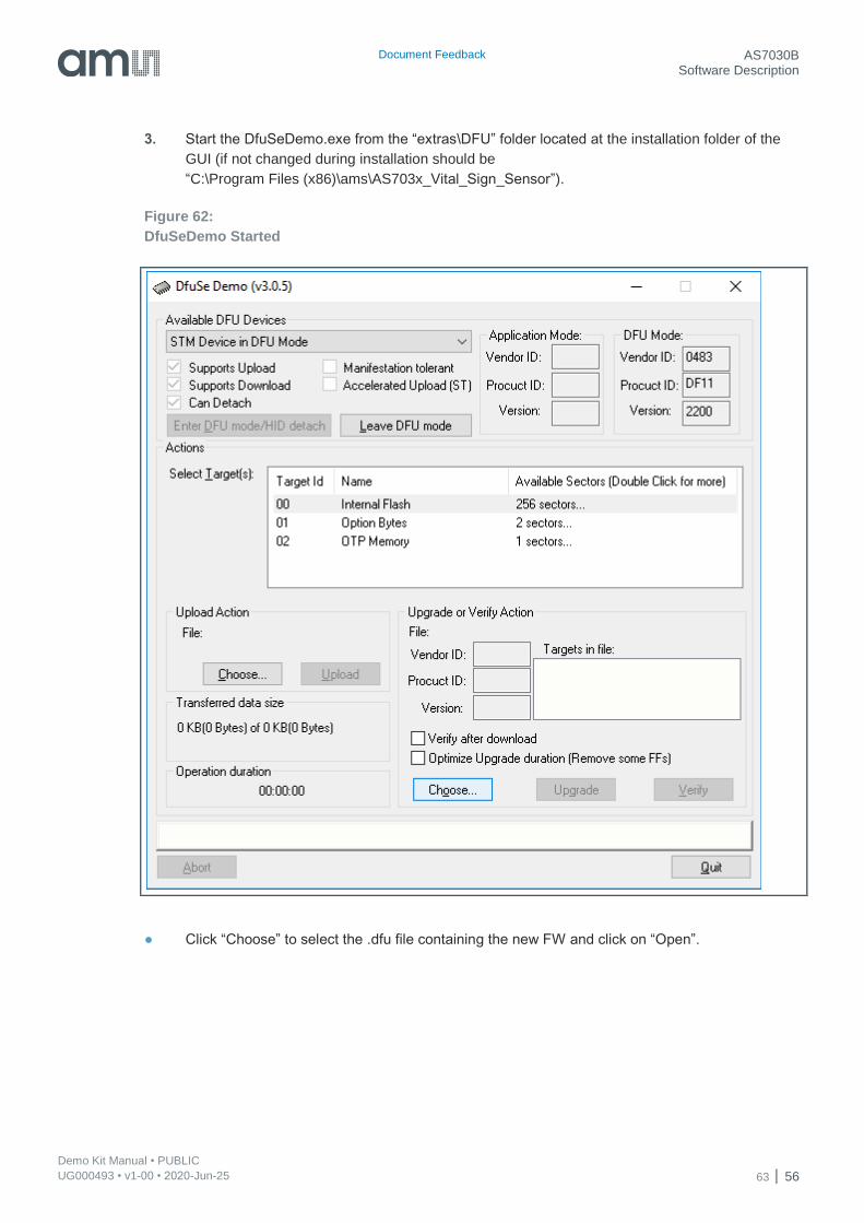
3. Start the DfuSeDemo.exe from the “extras\DFU” folder located at the installation folder of the
GUI (if not changed during installation should be
“C:\Program Files (x86)\ams\AS703x_Vital_Sign_Sensor”).
Figure 62:
DfuSeDemo Started
● Click “Choose” to select the .dfu file containing the new FW and click on “Open”.

Document Feedback AS7030B Software Description
Demo Kit Manual • PUBLIC UG000493 • v1-00 • 2020-Jun-25 63 │ 57
Figure 63:
Choosing Firmware DFU Package
● If the firmware was correctly loaded, the “Upgrade” button will be enabled, click on it to start the
upgrade process.
Document Feedback AS7030B Software Description
Demo Kit Manual • PUBLIC UG000493 • v1-00 • 2020-Jun-25 63 │ 58
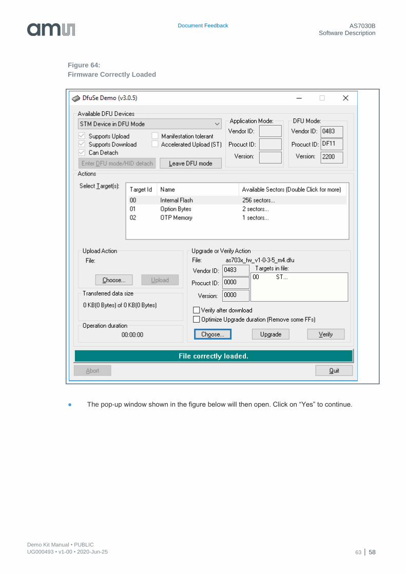
Figure 64:
Firmware Correctly Loaded
● The pop-up window shown in the figure below will then open. Click on “Yes” to continue.

Document Feedback AS7030B Software Description
Demo Kit Manual • PUBLIC UG000493 • v1-00 • 2020-Jun-25 63 │ 59
Figure 65:
Confirm Firmware Upgrade
● The upgrade process will start; upgrade status will be displayed at the bottom of the window.

Document Feedback AS7030B Software Description
Demo Kit Manual • PUBLIC UG000493 • v1-00 • 2020-Jun-25 63 │ 60
Figure 66:
Firmware Upgrade Ongoing
● After the FW upgrade finished, click on “Leave DFU mode”, then “Quit”.
Document Feedback AS7030B Software Description
Demo Kit Manual • PUBLIC UG000493 • v1-00 • 2020-Jun-25 63 │ 61
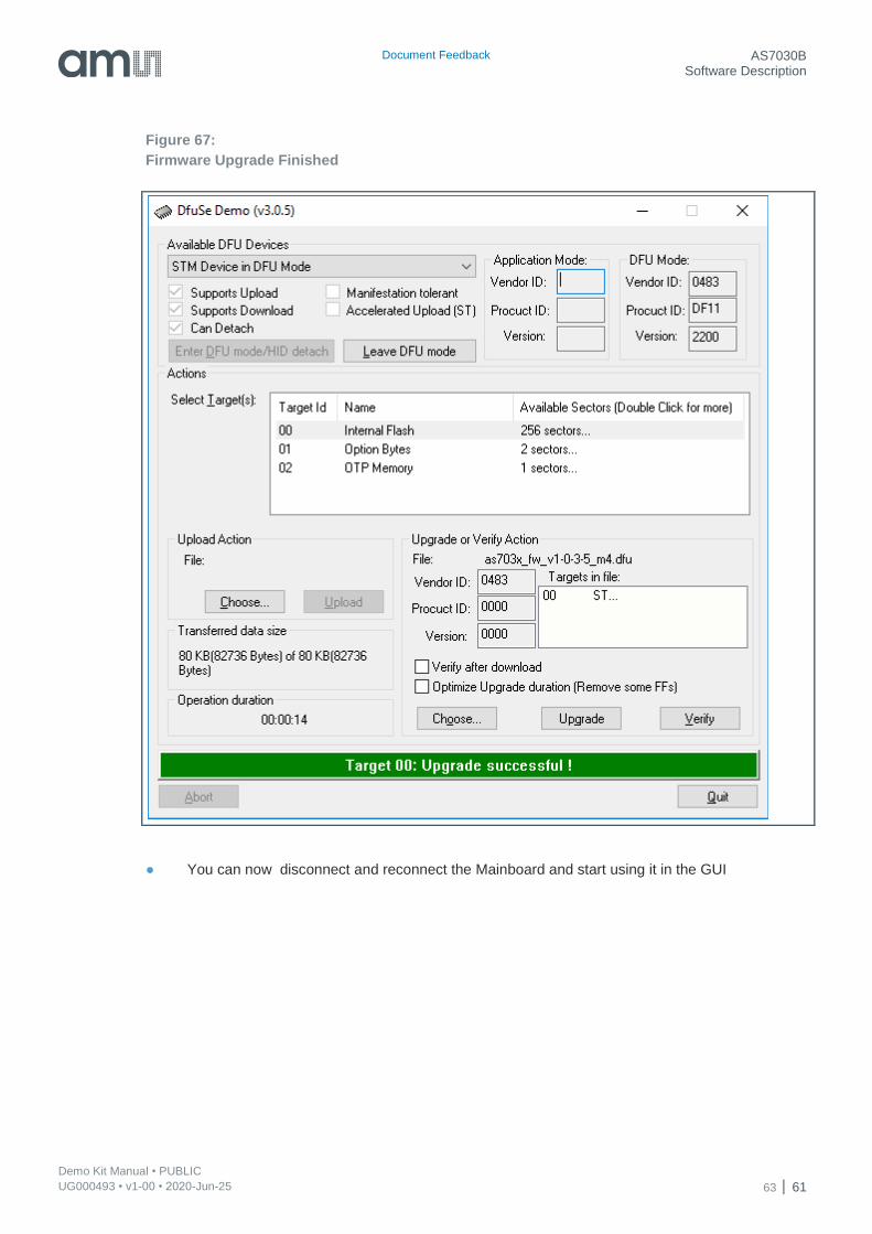
Figure 67:
Firmware Upgrade Finished
● You can now disconnect and reconnect the Mainboard and start using it in the GUI
Document Feedback AS7030B Revision Information
Demo Kit Manual • PUBLIC UG000493 • v1-00 • 2020-Jun-25 63 │ 62
6 Revision Information
Changes from previous version to current revision v1-00 Page
Initial version
● Page and figure numbers for the previous version may differ from page and figure numbers in the current revision.
● Correction of typographical errors is not explicitly mentioned.

Document Feedback AS7030B Legal Information
Demo Kit Manual • PUBLIC UG000493 • v1-00 • 2020-Jun-25 63 │ 63
7 Legal Information
Copyrights & Disclaimer
Copyright ams AG, Tobelbader Strasse 30, 8141 Premstaetten, Austria-Europe. Trademarks Registered. All rights reserved. The material herein may not be reproduced, adapted, merged, translated, stored, or used without the prior written consent of the copyright owner.
Demo Kits, Evaluation Kits and Reference Designs are provided to recipient on an “as is” basis for demonstration and evaluation purposes only and are not considered to be finished end-products intended and fit for general consumer use, commercial applications and applications with special requirements such as but not limited to medical equipment or automotive applications. Demo Kits, Evaluation Kits and Reference Designs have not been tested for compliance with electromagnetic compatibility (EMC) standards and directives, unless otherwise specified. Demo Kits, Evaluation Kits and Reference Designs shall be used by qualified personnel only.
ams AG reserves the right to change functionality and price of Demo Kits, Evaluation Kits and Reference Designs at any time and without notice.
Any express or implied warranties, including, but not limited to the implied warranties of merchantability and fitness for a particular purpose are disclaimed. Any claims and demands and any direct, indirect, incidental, special, exemplary or consequential damages arising from the inadequacy of the provided Demo Kits, Evaluation Kits and Reference Designs or incurred losses of any kind (e.g. loss of use, data or profits or business interruption however caused) as a consequence of their use are excluded.
ams AG shall not be liable to recipient or any third party for any damages, including but not limited to personal injury, property damage, loss of profits, loss of use, interruption of business or indirect, special, incidental or consequential damages, of any kind, in connection with or arising out of the furnishing, performance or use of the technical data herein. No obligation or liability to recipient or any third party shall arise or flow out of ams AG rendering of technical or other services.
RoHS Compliant & ams Green Statement
RoHS Compliant: The term RoHS compliant means that ams AG products fully comply with current RoHS directives. Our
semiconductor products do not contain any chemicals for all 6 substance categories plus additional 4 substance categories (per amendment EU 2015/863), including the requirement that lead not exceed 0.1% by weight in homogeneous materials. Where designed to be soldered at high temperatures, RoHS compliant products are suitable for use in specified lead-free processes.
ams Green (RoHS compliant and no Sb/Br/Cl): ams Green defines that in addition to RoHS compliance, our products are free of Bromine (Br) and Antimony (Sb) based flame retardants (Br or Sb do not exceed 0.1% by weight in homogeneous material) and do not contain Chlorine (Cl not exceed 0.1% by weight in homogeneous material).
Important Information: The information provided in this statement represents ams AG knowledge and belief as of the date that
it is provided. ams AG bases its knowledge and belief on information provided by third parties, and makes no representation or warranty as to the accuracy of such information. Efforts are underway to better integrate information from third parties. ams AG has taken and continues to take reasonable steps to provide representative and accurate information but may not have conducted destructive testing or chemical analysis on incoming materials and chemicals. ams AG and ams AG suppliers consider certain information to be proprietary, and thus CAS numbers and other limited information may not be available for release.
Headquarters
ams AG
Tobelbader Strasse 30
8141 Premstaetten
Austria, Europe
Tel: +43 (0) 3136 500 0
Please visit our website at www.ams.com
Buy our products or get free samples online at www.ams.com/Products
Technical Support is available at www.ams.com/Technical-Support
Provide feedback about this document at www.ams.com/Document-Feedback
For sales offices, distributors and representatives go to www.ams.com/Contact
For further information and requests, e-mail us at [email protected]


