© 2012
Analysis of innovation trends in packaging for power modules
7th European Advanced Technology Workshop on Micropackaging and Thermal Management
February 1st & 2nd – IMAPS 2012
Jean-Marc YANNOU, [email protected] Alexandre Avron, [email protected]
© 2012 • 2
Content
• Introduction – Standard module package cross section drawing
– Key innovation areas
• Die interconnection
• Die attach
• Substrates (DBC, baseplate) and encapsulation
• Focus on EV/HEV – Packaging trend in EV/HEV
– Case studies: GM, Denso, Honda…
• Conclusions
© 2012 • 3
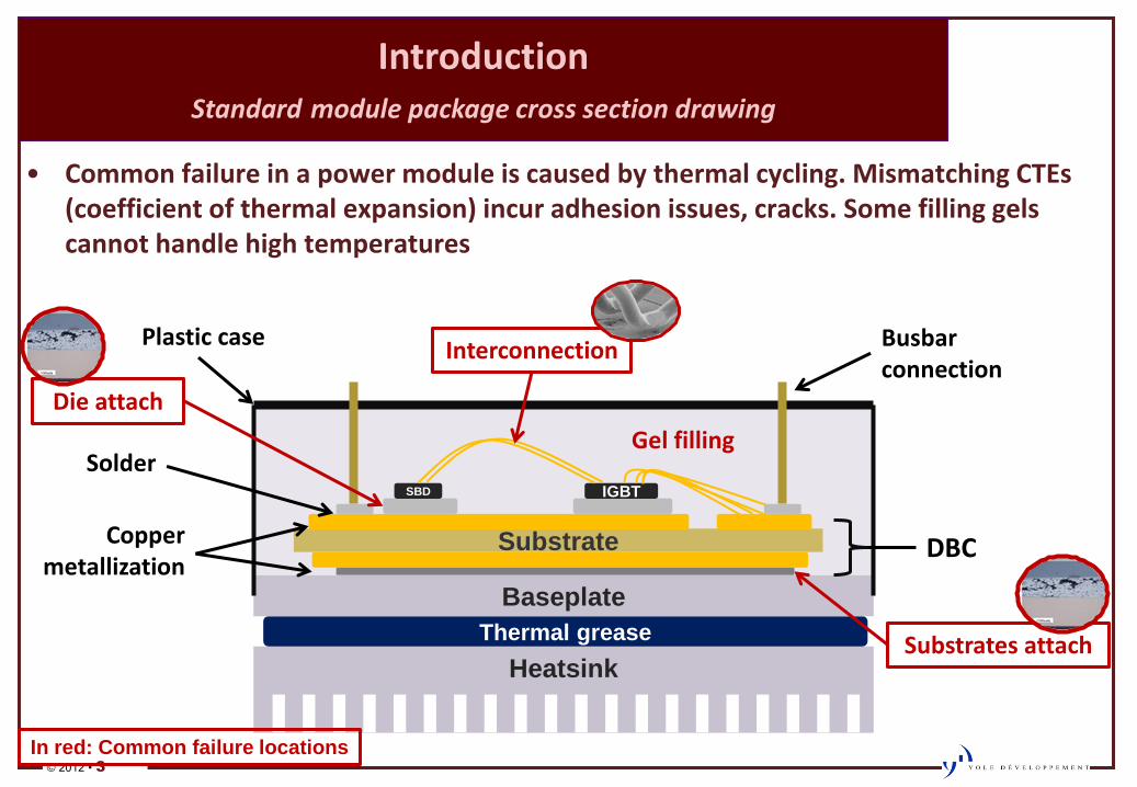
Introduction Standard module package cross section drawing
Heatsink
Thermal grease
Substrate
SBD IGBT
Baseplate
DBC
Busbar connection
Solder
Copper metallization
Plastic case
• Common failure in a power module is caused by thermal cycling. Mismatching CTEs (coefficient of thermal expansion) incur adhesion issues, cracks. Some filling gels cannot handle high temperatures
Die attach
Interconnection
Gel filling
Substrates attach
In red: Common failure locations
© 2012 • 4
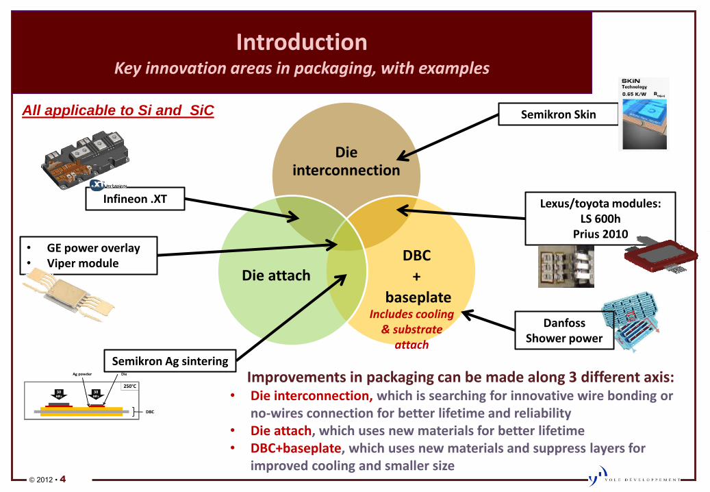
Introduction Key innovation areas in packaging, with examples
Die interconnection
DBC
+
baseplate
Die attach
Infineon .XT Lexus/toyota modules: LS 600h
Prius 2010
Semikron Ag sintering
Semikron Skin
• GE power overlay • Viper module
Improvements in packaging can be made along 3 different axis: • Die interconnection, which is searching for innovative wire bonding or
no-wires connection for better lifetime and reliability • Die attach, which uses new materials for better lifetime • DBC+baseplate, which uses new materials and suppress layers for
improved cooling and smaller size
All applicable to Si and SiC
Includes cooling & substrate
attach
Danfoss Shower power
© 2012 • 5
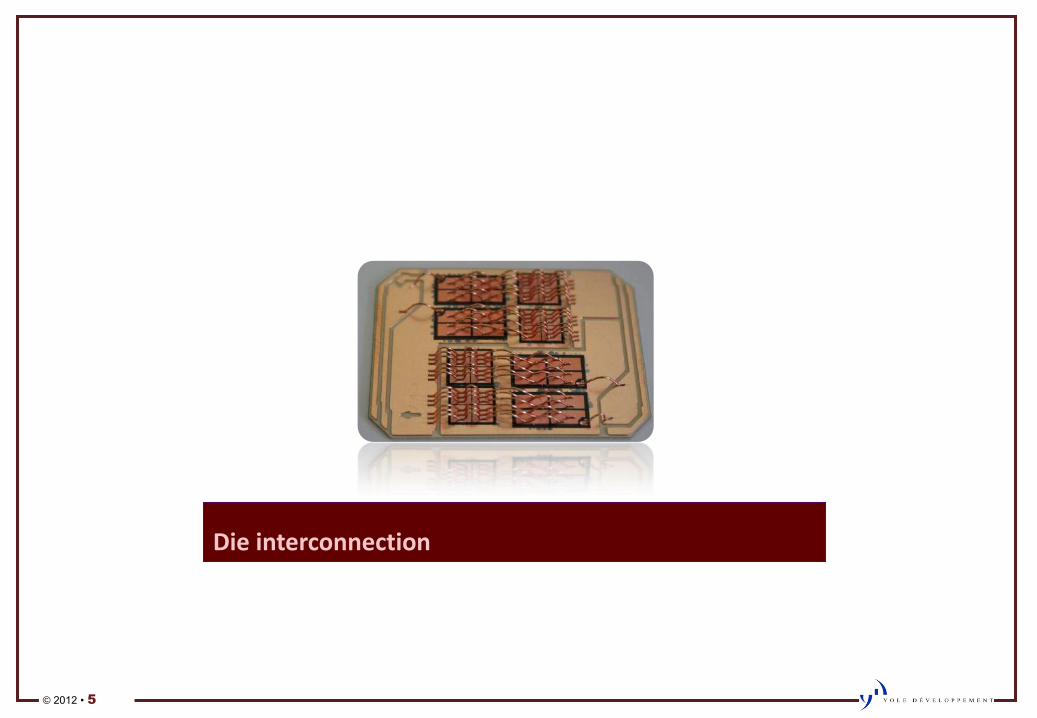
Die interconnection
© 2012 • 6
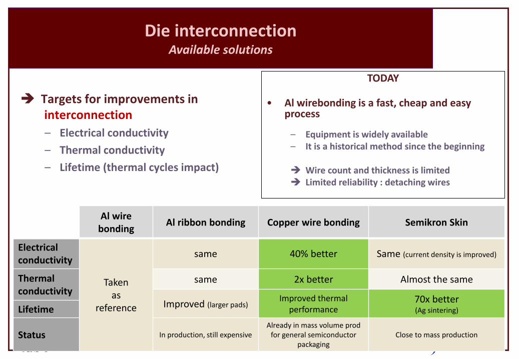
Die interconnection Available solutions
Targets for improvements in interconnection
– Electrical conductivity
– Thermal conductivity
– Lifetime (thermal cycles impact)
Al wire bonding
Al ribbon bonding Copper wire bonding Semikron Skin
Electrical conductivity
Taken as
reference
same 40% better Same (current density is improved)
Thermal conductivity
same 2x better Almost the same
Improved (larger pads) Improved thermal
performance 70x better (Ag sintering) Lifetime
Status In production, still expensive Already in mass volume prod
for general semiconductor packaging
Close to mass production
TODAY
• Al wirebonding is a fast, cheap and easy process
– Equipment is widely available – It is a historical method since the beginning
Wire count and thickness is limited Limited reliability : detaching wires

© 2012 • 7
Die interconnection Case study - Infineon .XT
• Infineon introduced mass production of copper wirebonding power modules
Copper Aluminum
Electrical resistivity 1,7µΩ.cm 2,7µΩ.cm
Thermal conductivity 400W/m.K 220W/m.K
Source: Infineon
Copper wire bonding is the next standard. Biggest are working towards this technology. Equipement is ready as copper wire bonders are widely used for low power and signal It is not expensive and easy to produce in mass compared to gold wires or flip-chip Remaining issue is die metallization Most important players are already working
towards this standard
© 2012 • 8
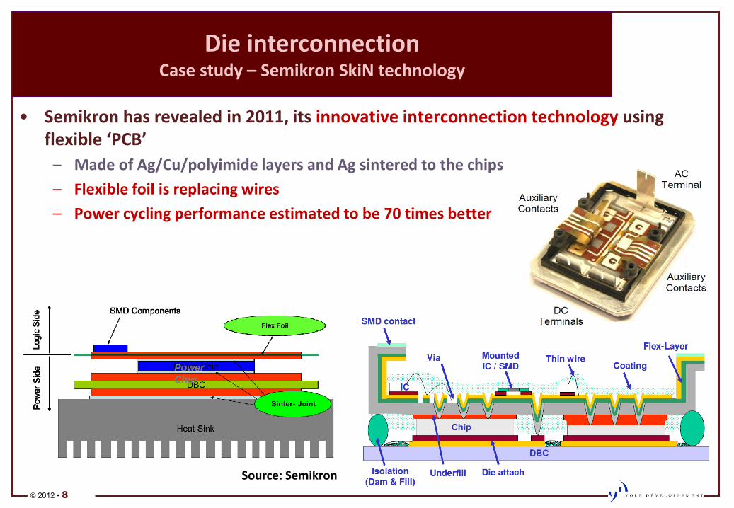
Die interconnection Case study – Semikron SkiN technology
• Semikron has revealed in 2011, its innovative interconnection technology using flexible ‘PCB’
– Made of Ag/Cu/polyimide layers and Ag sintered to the chips
– Flexible foil is replacing wires
– Power cycling performance estimated to be 70 times better
Power
Chip
Source: Semikron
© 2012 • 9
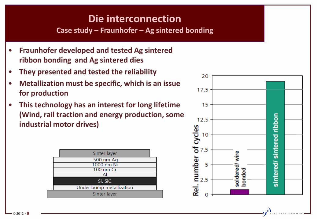
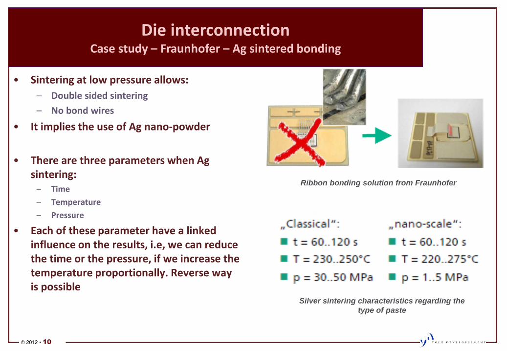
Die interconnection Case study – Fraunhofer – Ag sintered bonding
• Fraunhofer developed and tested Ag sintered ribbon bonding and Ag sintered dies
• They presented and tested the reliability
• Metallization must be specific, which is an issue for production
• This technology has an interest for long lifetime (Wind, rail traction and energy production, some industrial motor drives)
© 2012 • 10
Die interconnection Case study – Fraunhofer – Ag sintered bonding
• Sintering at low pressure allows:
– Double sided sintering
– No bond wires
• It implies the use of Ag nano-powder
• There are three parameters when Ag sintering: – Time
– Temperature
– Pressure
• Each of these parameter have a linked influence on the results, i.e, we can reduce the time or the pressure, if we increase the temperature proportionally. Reverse way is possible
Ribbon bonding solution from Fraunhofer
Silver sintering characteristics regarding the
type of paste

© 2012 • 11
Die attach
© 2012 • 12
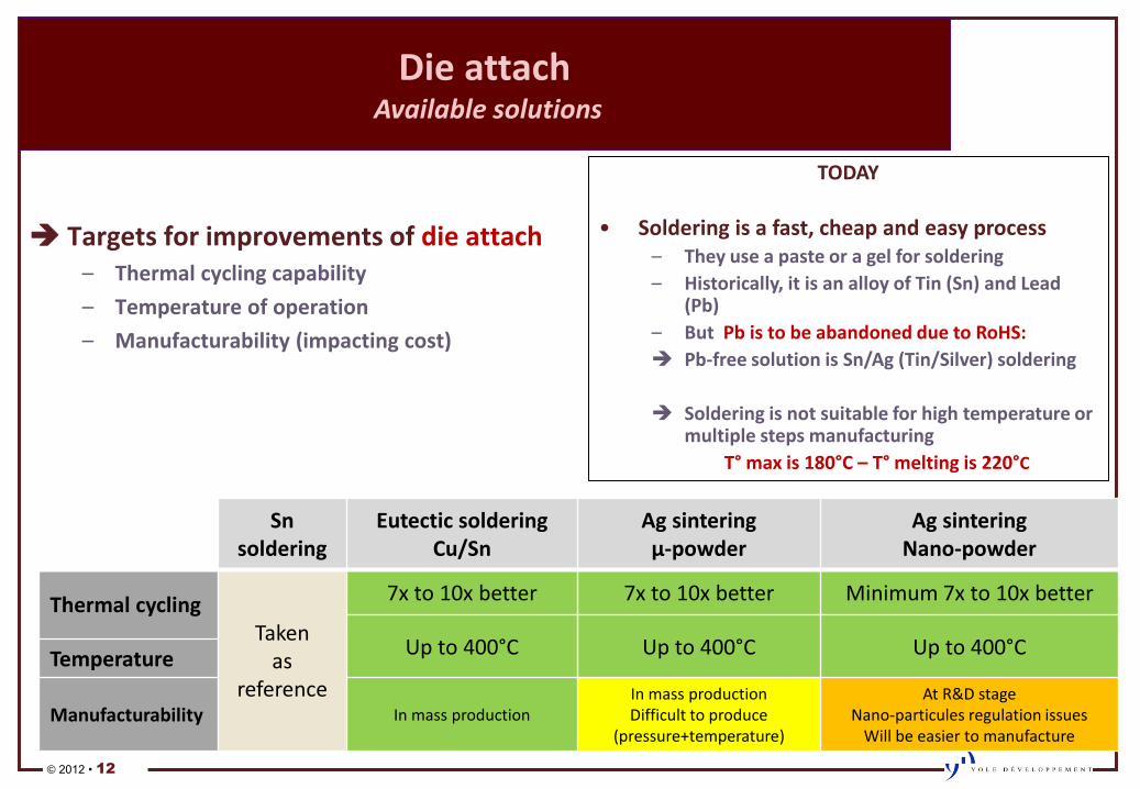
Die attach Available solutions
Targets for improvements of die attach – Thermal cycling capability
– Temperature of operation
– Manufacturability (impacting cost)
TODAY
• Soldering is a fast, cheap and easy process – They use a paste or a gel for soldering
– Historically, it is an alloy of Tin (Sn) and Lead (Pb)
– But Pb is to be abandoned due to RoHS:
Pb-free solution is Sn/Ag (Tin/Silver) soldering
Soldering is not suitable for high temperature or multiple steps manufacturing
T° max is 180°C – T° melting is 220°C
Sn soldering
Eutectic soldering Cu/Sn
Ag sintering µ-powder
Ag sintering Nano-powder
Thermal cycling Taken
as reference
7x to 10x better 7x to 10x better Minimum 7x to 10x better
Up to 400°C Up to 400°C Up to 400°C Temperature
Manufacturability In mass production In mass production Difficult to produce
(pressure+temperature)
At R&D stage Nano-particules regulation issues
Will be easier to manufacture
© 2012 • 13
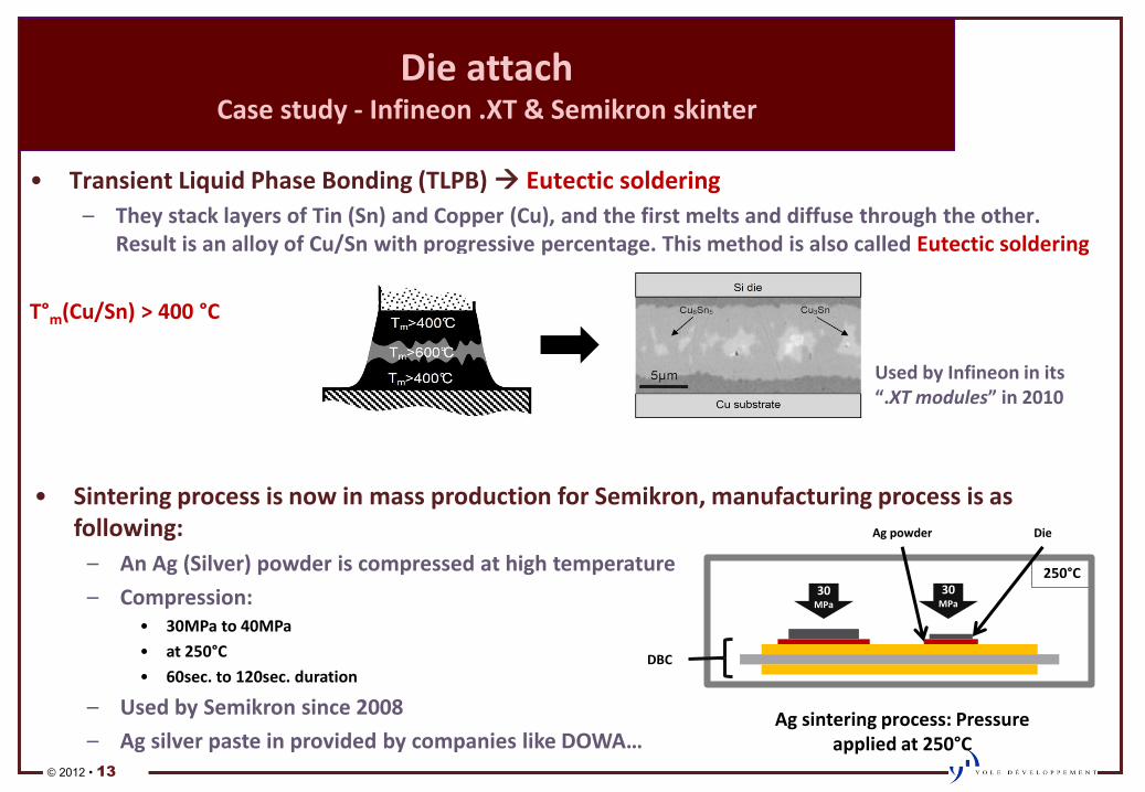
• Transient Liquid Phase Bonding (TLPB) Eutectic soldering
– They stack layers of Tin (Sn) and Copper (Cu), and the first melts and diffuse through the other. Result is an alloy of Cu/Sn with progressive percentage. This method is also called Eutectic soldering
T°m(Cu/Sn) > 400 °C
Die attach Case study - Infineon .XT & Semikron skinter
Used by Infineon in its “.XT modules” in 2010
• Sintering process is now in mass production for Semikron, manufacturing process is as following:
– An Ag (Silver) powder is compressed at high temperature
– Compression: • 30MPa to 40MPa
• at 250°C
• 60sec. to 120sec. duration
– Used by Semikron since 2008
– Ag silver paste in provided by companies like DOWA…
30 MPa
30 MPa
250°C
Die Ag powder
DBC
Ag sintering process: Pressure applied at 250°C
© 2012 • 14
Die attach Silver sintering
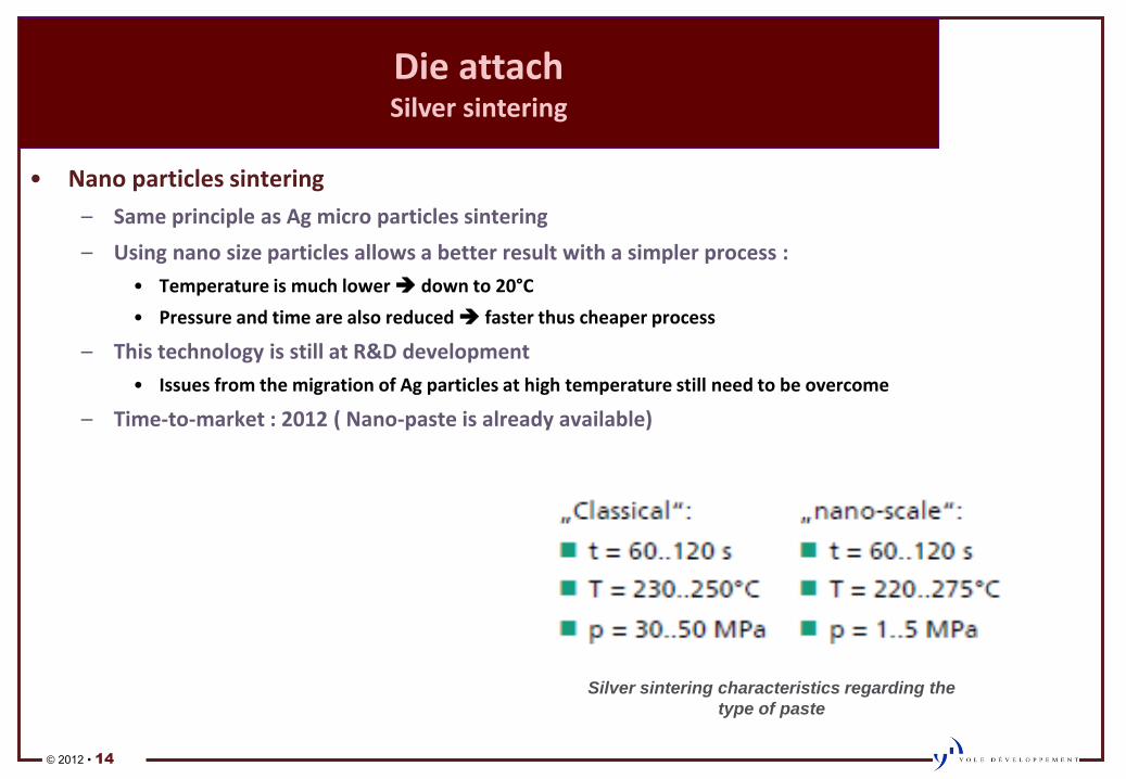
• Nano particles sintering
– Same principle as Ag micro particles sintering
– Using nano size particles allows a better result with a simpler process :
• Temperature is much lower down to 20°C
• Pressure and time are also reduced faster thus cheaper process
– This technology is still at R&D development
• Issues from the migration of Ag particles at high temperature still need to be overcome
– Time-to-market : 2012 ( Nano-paste is already available)
Silver sintering characteristics regarding the
type of paste
© 2012 • 15
DBC, Baseplate and encapsulation
© 2012 • 16
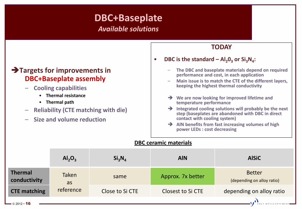
DBC+Baseplate Available solutions
Targets for improvements in DBC+Baseplate assembly – Cooling capabilities
• Thermal resistance
• Thermal path
– Reliability (CTE matching with die)
– Size and volume reduction
Al2O3 Si3N4 AlN AlSiC
Thermal conductivity
Taken as
reference
same Approx. 7x better Better
(depending on alloy ratio)
CTE matching Close to Si CTE Closest to Si CTE depending on alloy ratio
TODAY
• DBC is the standard – Al203 or Si3N4:
– The DBC and baseplate materials depend on required performance and cost, in each application
– Main issue is to match the CTE of the different layers, keeping the highest thermal conductivity
We are now looking for improved lifetime and temperature performance
Integrated cooling solutions will probably be the next step (baseplates are abandoned with DBC in direct contact with cooling system)
AlN benefits from fast increasing volumes of high power LEDs : cost decreasing
DBC ceramic materials
© 2012 • 17
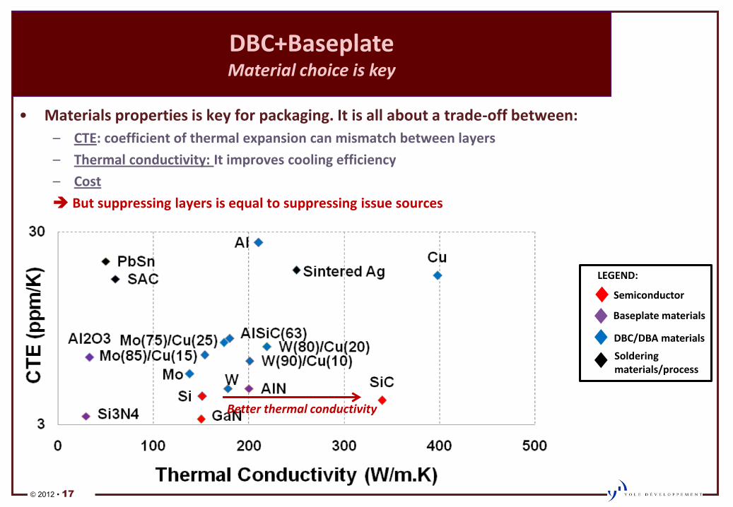
DBC+Baseplate Material choice is key
• Materials properties is key for packaging. It is all about a trade-off between:
– CTE: coefficient of thermal expansion can mismatch between layers
– Thermal conductivity: It improves cooling efficiency
– Cost
But suppressing layers is equal to suppressing issue sources
Baseplate materials
DBC/DBA materials
Soldering materials/process
LEGEND:
Semiconductor
Better thermal conductivity
© 2012 • 18
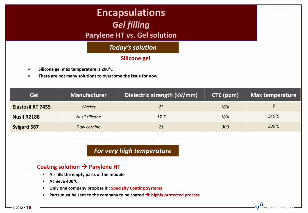
Encapsulations Gel filling
Parylene HT vs. Gel solution
– Coating solution Parylene HT • Air fills the empty parts of the module
• Achieve 400°C
• Only one company propose it : Specialty Coating Systems
• Parts must be sent to the company to be coated highly protected process
Gel Manufacturer Dielectric strength (kV/mm) CTE (ppm) Max temperature
Elastosil RT 745S Wacker 23 N/A ?
Nusil R2188 Nusil silicone 17.7 N/A 240°C
Sylgard 567 Dow corning 21 300 200°C
Silicone gel
• Silicone gel max temperature is 200°C
• There are not many solutions to overcome the issue for now
For very high temperature
Today’s solution
© 2012 • 19
FOCUS ON EV/HEV

© 2012 • 20
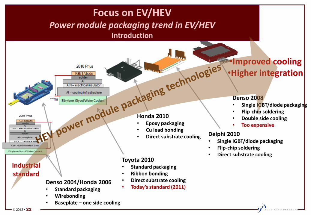
Focus on EV/HEV Power module packaging trend in EV/HEV
Introduction
3.0 mm
9.0mm
Denso 2004/Honda 2006 • Standard packaging • Wirebonding • Baseplate – one side cooling
Toyota 2010 • Standard packaging • Ribbon bonding • Direct substrate cooling • Today’s standard (2011)
Honda 2010 • Epoxy packaging • Cu lead bonding • Direct substrate cooling Delphi 2010
• Single IGBT/diode packaging • Flip-chip soldering • Direct substrate cooling
Denso 2008 • Single IGBT/diode packaging • Flip-chip soldering • Double side cooling • Too expensive
•Improved cooling •Higher integration
Industrial standard
• EV/HEV is one of the biggest market for power electronics in 2020, according to all forecasts
• The main challenges will include manufacturability, reliability and lifetime, but also integration and weight
• Module packaging is already a great challenge in EV/HEV: • The market is potentially large enough to involve large development efforts • The level of integration will lead to custom solutions and all integrated
inverters • Footprint, size, weight and cost and all are strong technical drivers
© 2012 • 21
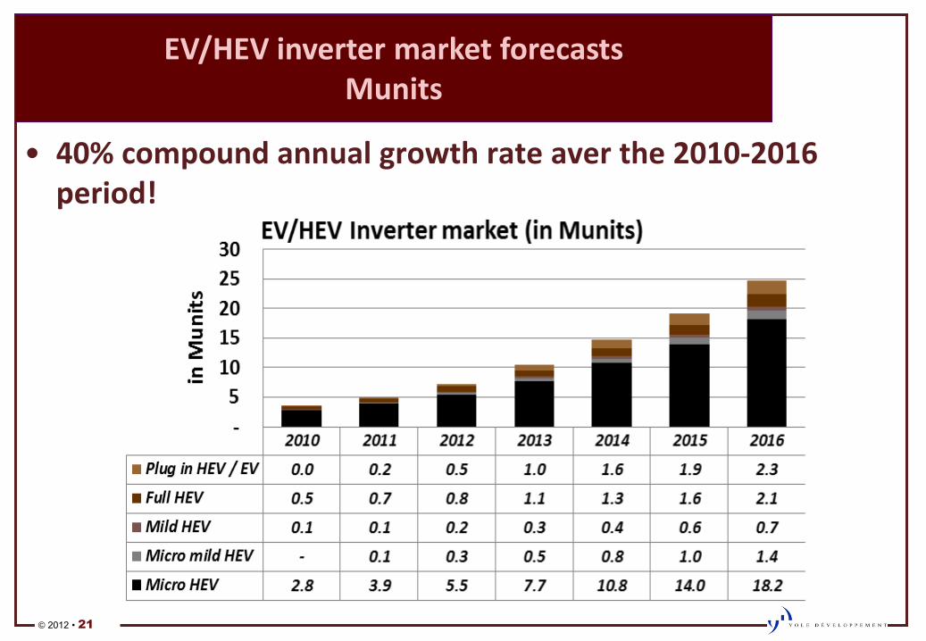
EV/HEV inverter market forecasts Munits
• 40% compound annual growth rate aver the 2010-2016 period!
© 2012 • 22
Focus on EV/HEV Power module packaging trend in EV/HEV
Introduction
3.0 mm
9.0mm
Denso 2004/Honda 2006 • Standard packaging • Wirebonding • Baseplate – one side cooling
Toyota 2010 • Standard packaging • Ribbon bonding • Direct substrate cooling • Today’s standard (2011)
Honda 2010 • Epoxy packaging • Cu lead bonding • Direct substrate cooling Delphi 2010
• Single IGBT/diode packaging • Flip-chip soldering • Direct substrate cooling
Denso 2008 • Single IGBT/diode packaging • Flip-chip soldering • Double side cooling • Too expensive
•Improved cooling •Higher integration
Industrial standard
© 2012 • 23
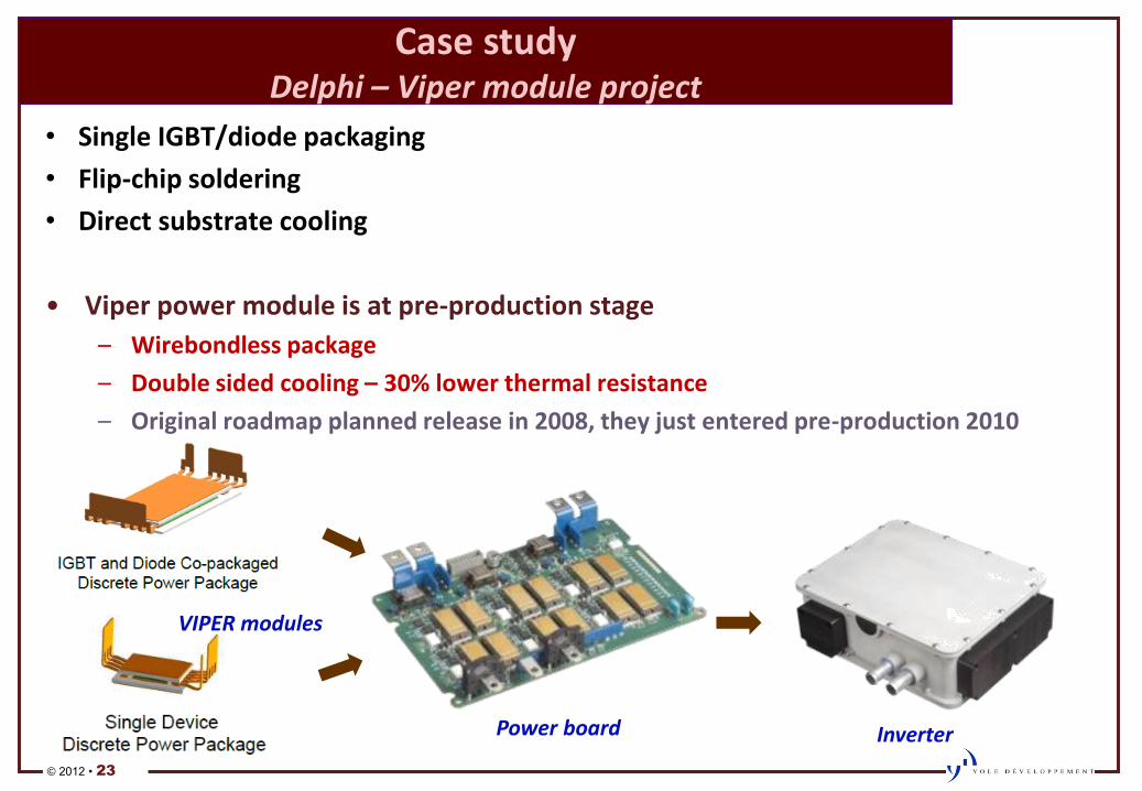
Case study Delphi – Viper module project
• Single IGBT/diode packaging
• Flip-chip soldering
• Direct substrate cooling
• Viper power module is at pre-production stage
– Wirebondless package
– Double sided cooling – 30% lower thermal resistance
– Original roadmap planned release in 2008, they just entered pre-production 2010
VIPER modules
Power board Inverter
© 2012 • 24
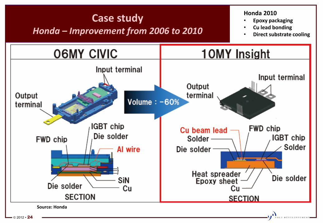
Case study Honda – Improvement from 2006 to 2010
Source: Honda
Honda 2010 • Epoxy packaging • Cu lead bonding • Direct substrate cooling
© 2012 • 25
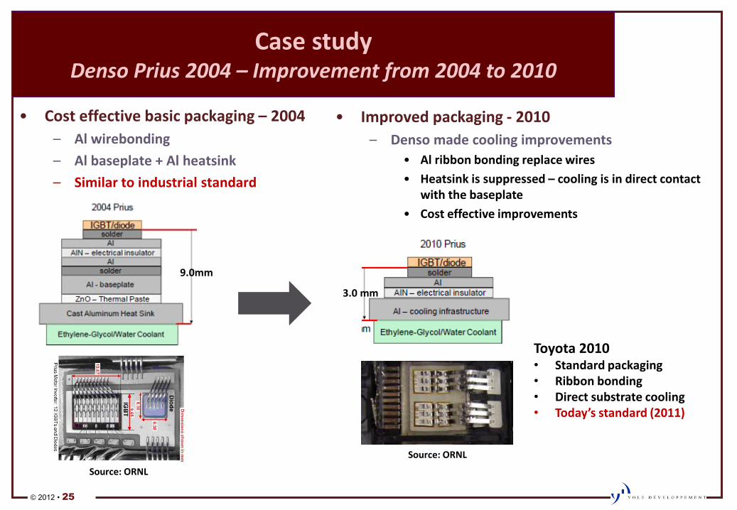
Case study Denso Prius 2004 – Improvement from 2004 to 2010
• Cost effective basic packaging – 2004
– Al wirebonding
– Al baseplate + Al heatsink
– Similar to industrial standard
9.0mm
Source: ORNL
Source: ORNL
• Improved packaging - 2010
– Denso made cooling improvements
• Al ribbon bonding replace wires
• Heatsink is suppressed – cooling is in direct contact with the baseplate
• Cost effective improvements
3.0 mm
Toyota 2010 • Standard packaging • Ribbon bonding • Direct substrate cooling • Today’s standard (2011)
© 2012 • 26
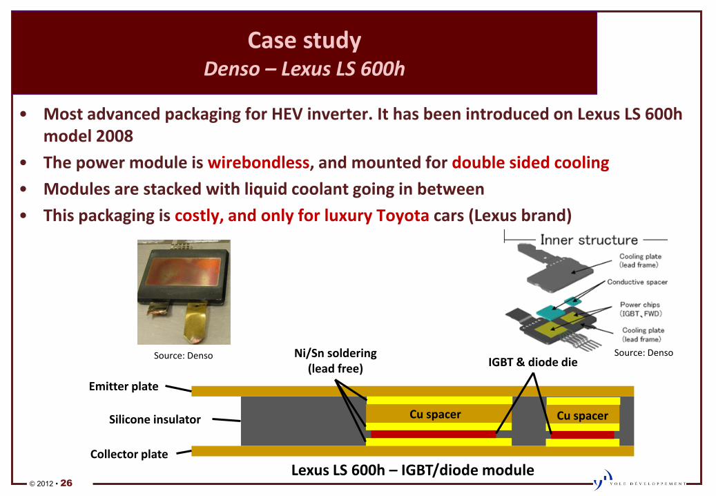
Case study Denso – Lexus LS 600h
• Most advanced packaging for HEV inverter. It has been introduced on Lexus LS 600h model 2008
• The power module is wirebondless, and mounted for double sided cooling
• Modules are stacked with liquid coolant going in between
• This packaging is costly, and only for luxury Toyota cars (Lexus brand)
Emitter plate
Collector plate
Silicone insulator
Ni/Sn soldering (lead free)
Cu spacer Cu spacer
IGBT & diode die
Lexus LS 600h – IGBT/diode module
Source: Denso Source: Denso
© 2012 • 27
Conclusions
© 2012 • 28
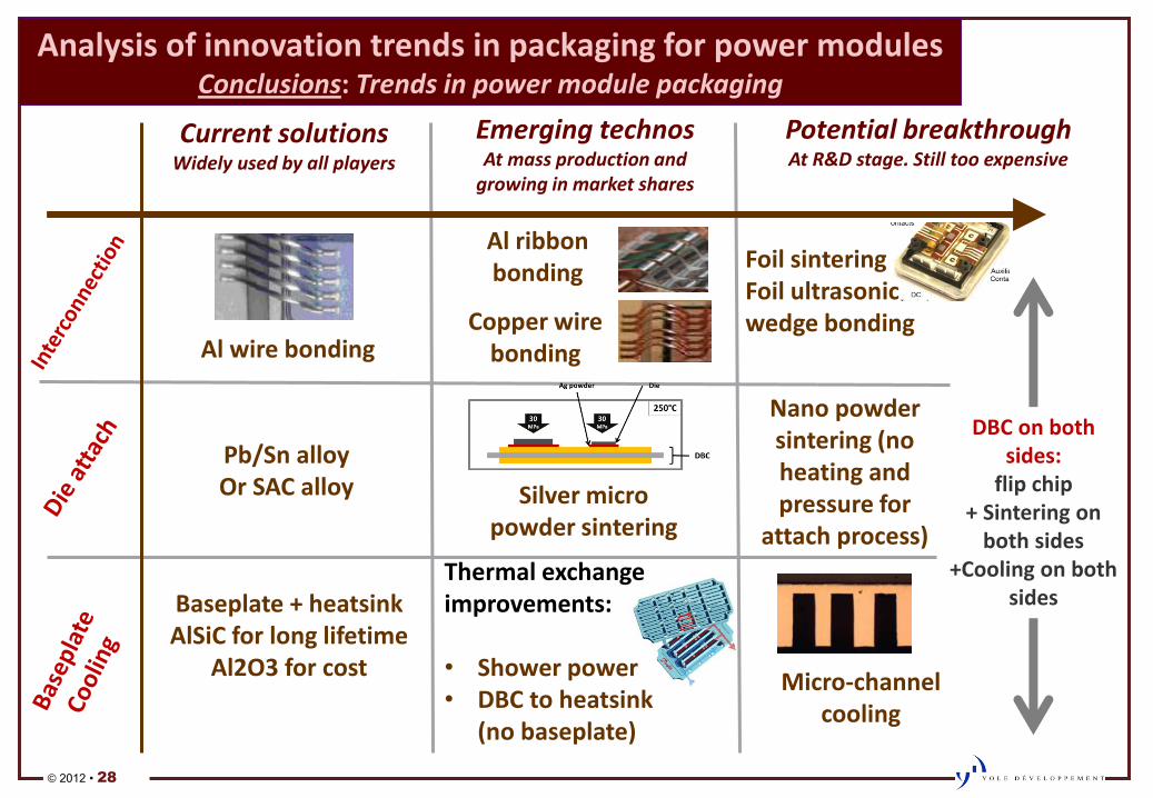
Analysis of innovation trends in packaging for power modules Conclusions: Trends in power module packaging
Current solutions Widely used by all players
Emerging technos At mass production and
growing in market shares
Potential breakthrough At R&D stage. Still too expensive
Pb/Sn alloy Or SAC alloy Silver micro
powder sintering
Al wire bonding
Al ribbon bonding
Copper wire bonding
DBC on both sides:
flip chip + Sintering on
both sides +Cooling on both
sides Baseplate + heatsink AlSiC for long lifetime
Al2O3 for cost
Thermal exchange improvements: • Shower power • DBC to heatsink
(no baseplate)
Micro-channel cooling
Nano powder sintering (no heating and pressure for
attach process)
Foil sintering Foil ultrasonic wedge bonding
© 2012 • 29
Analysis of innovation trends in packaging for power modules Conclusions
• The main improvements aspects are each leading to different technologies, but some breakthrough technologies are promising to solve all these issues at the same time: – Using double side DBC, with integrated cooling could solve all the potential issues at the same
time. But production process is not cost effective as of today, and no standard is emerging yet
• Several technologies are closer in time or already used in high-end packaging: – Direct cooling is becoming a standard and widely used, especially for EV/HEV. There is no clear
trend in wirebonding: • Copper wires seems on its way to become a standard, being developed by several players including Infineon • Semikron pushes for Ag sintering applied to interconnection, but we have to wait and see for the results • Denso is putting ribbon Al bonding in Toyota Prius modules
– Die attach solutions are on the same trends, between copper and Ag sintering
• The innovation is going to be increasingly driven by EV/HEV players. They need better power electronics conversion systems to gain in added value. Smaller and easier to cool are the two drivers.
© 2012 • 30
Your contacts at YOLE
• Your contacts at YOLE Développement: – Brice Le Gouic, Alexandre Avron, Market
analysts in charge of Power Electronics activities • Email: [email protected]
• Tel: +33 472 83 01 81
– Jean-Marc Yannou, Market analyst in advanced packaging • Email: [email protected]
• Tel: +33 686 79 71 21
– Jean-Christophe Eloy, CEO: • Email: [email protected]
• Tel: +33 472 83 01 82
© 2012 • 31
BACKUP SLIDES
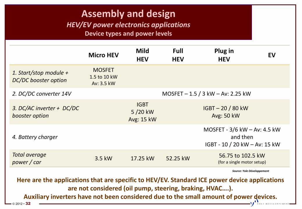
© 2012 • 32
Assembly and design HEV/EV power electronics applications
Device types and power levels
Micro HEV Mild HEV
Full HEV
Plug in HEV
EV
1. Start/stop module + DC/DC booster option
MOSFET 1.5 to 10 kW Av: 3.5 kW
2. DC/DC converter 14V MOSFET – 1.5 / 3 kW – Av: 2.25 kW
3. DC/AC inverter + DC/DC booster option
IGBT 5 /20 kW
Avg: 15 kW
IGBT – 20 / 80 kW Avg: 50 kW
4. Battery charger MOSFET - 3/6 kW – Av: 4.5 kW
and then IGBT - 10 / 20 kW – Av: 15 kW
Total average power / car
3.5 kW 17.25 kW 52.25 kW 56.75 to 102.5 kW (for a single motor setup)
Here are the applications that are specific to HEV/EV. Standard ICE power device applications are not considered (oil pump, steering, braking, HVAC….).
Auxiliary inverters have not been considered due to the small amount of power devices.
Source: Yole Développement
© 2012 • 33
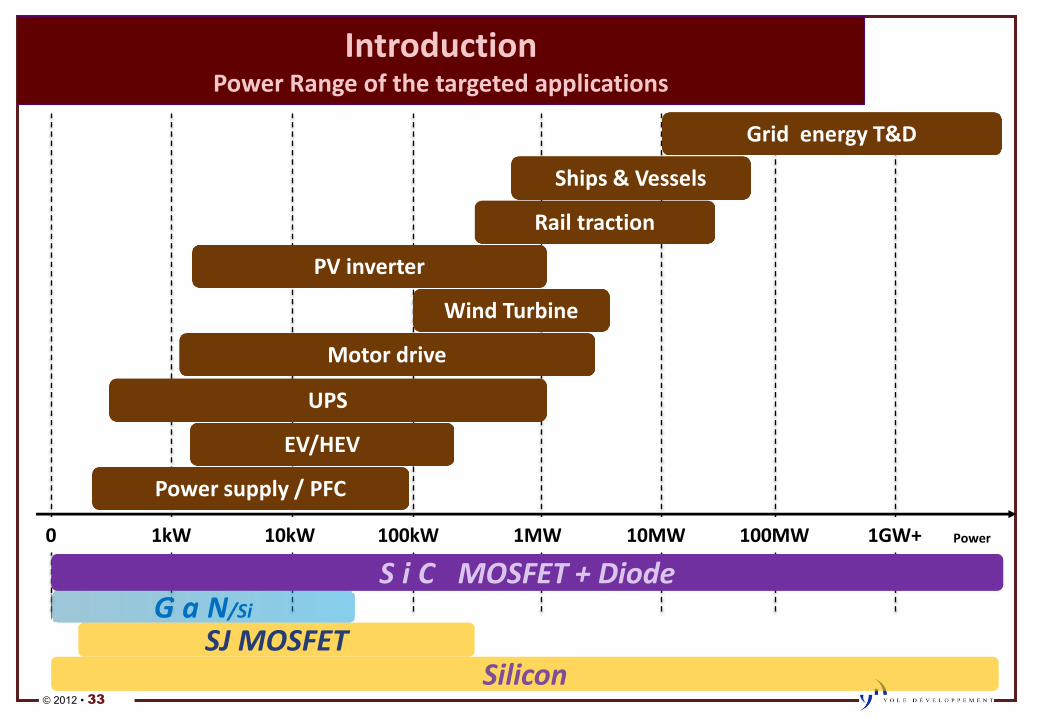
Introduction Power Range of the targeted applications
Power
Power supply / PFC
EV/HEV
UPS
Motor drive
Wind Turbine
PV inverter
Rail traction
Grid energy T&D
Ships & Vessels
1kW 100kW 0 10kW 1MW 10MW 100MW 1GW+
SJ MOSFET
S i C MOSFET + Diode G a N/Si
Silicon


