1
3D Behavior of Schottky Barriers of 2D Transition-
Metal Dichalcogenides
Yuzheng Guo1, Dameng Liu
2, John Robertson
1
1Department of Engineering, Cambridge University, Cambridge CB2 1PZ, United Kingdom
2State Key Laboratory of Tribology, Tsinghua University, Beijing 100084, China
The transition metal dichalcogenides (TMDs) are two-dimensional layered solids with van der
Waals bonding between layers. We calculate their Schottky barrier heights (SBHs) using super-
cell models and density functional theory. It is found that the SBHs without defects are quite
strongly pinned, with a pinning factor S of about S=0.3, a similar value for both top and edge
contact geometries. This arises because there is direct bonding between the contact metal atoms
and the TMD chalcogen atoms, for both top and edge contact geometries, despite the weak
interlayer bonding in the isolated materials. The Schottky barriers largely follow the metal
induced gap state (MIGS) model, like those of three-dimensional semiconductors, despite the
bonding in the TMDs being largely constrained within the layers. The pinning energies are found
to be lower in the gap for edge contact geometries than for top contact geometries, which might
be used to obtain p-type contacts on MoS2.
2
The transition metal dichalcogenides (TMDs) (MX2, where M=Mo/W; X=S/Se/Te) are
valuable two-dimensional systems, which unlike graphene are semiconductors with a band gap1
and so are useful for field effect transistors (FETs) 2-16
. They are particularly useful because they
make ultra-thin body devices4 and are suitable for end of the roadmap logic devices such as
tunnel FETs (TFETs) 5,6
. The carrier mobilities of TMDs are reasonably high, but it is known
experimentally that their device performances tend to be limited by their contact resistance11, 12
.
It appears that most contacts possess Schottky barriers and are not ohmic11
.
There is a desire to control the Schottky barrier heights (SBHs) by varying the contact metal so
as to try to minimize contact resistance. Due to the van der Waals inter-layer bonding, it might
be expected that the contact metal is also weakly bonded to the MX2 layer, so that the SBH
would vary strongly with contact metal work function, and the Schottky barrier might approach
the Schottky limit of weak pinning17
. This would allow the contact properties to be easily
controlled just by varying the metal work function. In practice, this seems not to occur; the SBH
seems to be quite strongly pinned11
. The SBH also seems to depend quite strongly on process
conditions, indicating the presence of process-induced defects18
. Furthermore, the contact Fermi
energy is generally pinned in the upper half of the band gap in MoS2, which favors n-type
devices11
. As bipolar devices are desirable for some applications, it is useful to know if these are
possible for MoS2 itself using high work function electrodes19, 20
, or if different TMDs are
needed for p-type devices14-16
.
A better understanding of the Schottky barriers in TMDs is desirable. Fermi level pinning
arises from the presence of interface gap states in the TMD which can generally be either due to
intrinsic states or to defect states. The least pinning occurs in the defect-free case. There have

3
been previous calculations of ideal, defect-free SBs for TMDs21-26
, but less extensive than those
given here. Here, we provide a comprehensive calculation of Schottky barrier heights of four
TMDs with twelve metals (Sc, Mg, Al, Ti, Cr, Mo, Ru, Co, Ni, Pd, Pt, MoO3) covering a wide
range of work functions, for both on-top and edge contact geometries. We show that the defect-
free SBHs in fact follow the metal induced gap state (MIGS) model27-31
that applies to three-
dimensional semiconductors, so that relatively strong Fermi level pinning is expected even for
defect-free interfaces. Any defects that do form will then cause additional pinning and lower the
S value. This insight provides a framework to understand TMD contacts as a whole.
Method
Here, the electronic structure of metal contacts on TMDs is studied directly using density
functional theory (DFT) calculations on supercells containing layers of metal and a monolayer of
TMD or metal on a block of TMD layers representing the bulk TMD. We use supercells with
TMD, metal and no vacuum. We use 6 layers of TMD to represent the bulk TMD, as this is large
enough for its gap to be within 0.05 eV of the bulk value32
. We choose six layers of metal in the
face-centered cubic or the body-centered cubic structure. For most metals, the (111) face of the
metal is placed on a hexagonal 2x2 supercell of the TMD, and the metal supercell lattice constant
is forced to match the TMD cell lattice constant (Fig 1a-c). The metal is allowed to relax
perpendicular to the layers, to conserve its volume, which is important because the atomic
volume is the main factor determining a metal’s work function33
. For most metals, the lattice
mismatch is under 6%, but test calculations with other mismatches in supercells with up to 8x8
lateral cells (0.5% lattice mismatch) were carried out to test the stability of our results. Generally,
no symmetry is applied within the supercell, as this allows the contact metal atoms to relax
4
around the MX2 atoms. For the Sc case, the Sc atom is much larger and a 1x1 Sc lattice fits on a
2x2 MX2 supercell. However, here we fix the symmetry for the case of Sc, to stop a reaction
between Sc and the MoS2 which leads to Sc sulfide formation, and which we want to avoid. We
also include MoO3:MoS2 interfaces to study a high work function case. Here, we use models
with a 4×5 supercell of MoS2 for a good lattice match.
The electronic structure is calculated using the CASTEP plane wave DFT code34
with the
electronic interaction modeled by the PBE style generalized gradient approximation, ultrasoft
pseudopotentials and without spin-orbit coupling (not yet included in CASTEP). A cutoff energy
of 480 eV converges the total energy to less than 0.01 eV per atom. The DFT errors for van der
Waals bonding are corrected using the Grimme35, 36
scheme. The screened exchange (SX) hybrid
functional37
is used to correct the band gap error of DFT where necessary. Hybrid functionals
correct well the band gap error for 3D and bulk 2D semiconductors. But they under-estimate the
quasi-particle gap of monolayer 2D semiconductors because of the large exciton energies38,39
in
these poorly screened systems.
The (p-type) Schottky barrier height is the energy difference between the valence band
maximum (VBM) and the metal Fermi level, Ef. In practice, this can be difficult to extract from
the interface band structures or local density of states because of a strong hybridization between
the metal states and the TMD states22
. We therefore use a reference energy method, in which the
Mo 4s or W 5s semi-core level is used as a reference level in the supercell system to derive the
metal Ef and the VBM energies from this reference level, and thus the SBH is derived as the
difference between these two values. This is the theoretical analogue of Kraut’s40
method in
photoemission.
Results and Discussion

5
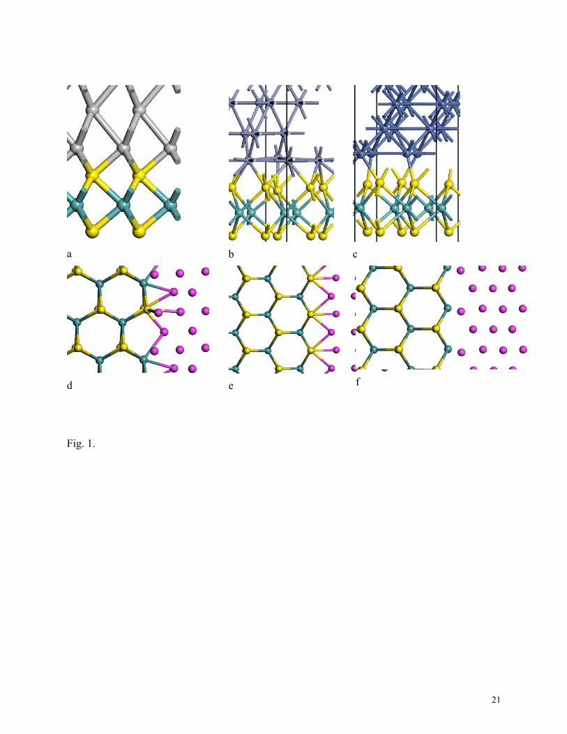
Fig. 2 plots the calculated values of the SBHs for monolayer (ML) and bulk MoS2 against the
metal work functions. We used 11 metals to cover a wide range of work functions from Sc (3.5
eV) to Pt (5.65 eV), and we also included MoO3 at 6.6 eV. The experimental work function
values are taken from Michaelson41
. The SBHs are seen to follow a linear dependence quite
closely, despite the different metal reactivities,
p = E0 + S(M – E0) (1)
Here, E0 is a reference energy of the gap states that pin the Fermi energies at the SBH. If the
pinning is due to intrinsic states such as MIGS, then E0 would be the charge neutrality level
(CNL). The CNL is the energy up to which the MIGS are filled on a neutral surface. The slope
S=dp/dΦM is the pinning factor. It varies between S=1 for unpinned interfaces (Schottky limit)
to S=0 for strongly pinned interfaces (Bardeen limit)28,29
. S can be related for the general case to
the density of interface gap states that cause the pinning, N, by42
0
2
1
1
eNS
(2)
where δ is the decay length of these states and 0 is the dielectric constant around the interface.
Thus, S varies inversely with N, and a large N gives a small S.
In order to display the SBH results for different TMDs, or the bulk and monolayer cases on
the same diagrams, we align the bands by their CNLs27,28
and express the barrier heights with
respect to the isotropically averaged CNLs. The CNLs are calculated from the band energies of
the isolated semiconductors30
, using the SX band energies to avoid the band gap error (Table 1).
6
In Fig. 2, we see that the slope S has a similar value for both the monolayer (S=0.28) and
bulk (S=0.33) cases. The value of S=0.28 for a monolayer compares to previous calculated
values of S~0.3 by Kang et al25
, and by Gong et al22
. This value of S~0.3 indicates moderate
Fermi level pinning. It compares to an experimental value of S=0.1 found by Das et al11
,
indicating strong pinning. From Eqn. (2), this stronger pinning than the MIGS model must arise
from the presence of extra gap states, and we argue elsewhere43,44
that these states are due to
defects as proposed experimentally18
.
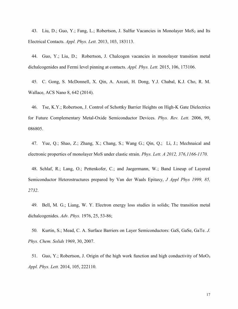
We next consider the edge contact geometry. Here, the metal layer bonds directly to the
MX2 planes. In this geometry, the metals bond directly to the TMD layers via covalent bonds.
This geometry is the same as for contacts on three-dimensional semiconductors, so that strong
pinning can be expected. The benefits of edge contacts were recently noted for graphene45
, where
they greatly increase the effective mobilities. We consider only the monolayer case. There are
three possible edge contact geometries for MX2 as shown in Fig 1(d-f); the non-polar armchair
interface where the metal bonds to both Mo and S sites, the zigzag S-terminated interface where
the metal bonds to S sites, and the zigzag Mo-terminated interface where the metal bonds to Mo
sites.
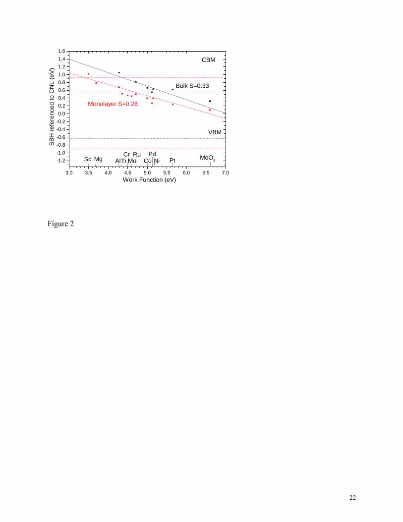
Fig 3(a) shows the calculated p-type SBHs for these three cases for monolayer MoS2,
referenced to the VBM, and including the SBH values for the top-contact geometry for reference.
A notable result is that the slopes S are very similar for all three edge contact cases, and also very
similar to that for the top contact case. The similar S values emphasize that the same degree of
pinning occurs in each case, which from (2) implies a similar density of gap states is causing the
pinning in each case. It suggests that the bonding is quite similar in both cases, as discussed
below.

7
The second notable result is that the SBH value is similar for the three different edge contact
geometries, despite the very different bonding types, with unlike or like atom bonds. The typical
cause of a shift in barrier heights is the presence of an interfacial dipole layer for the polar
interfaces46
. The absence of a significant shift suggests that the Mo-S bonding is not very polar,
and that any dipole is small. Indeed, we calculate a Mulliken charge for MoS2 of +0.30 e for Mo
and –0.15 e for S, indicating that MoS2 is not very ionic.
A third result is that the p-type SBH is ~0.7 eV lower for edge contacts than for top contacts.
As the previous result showed that any dipole layers due to polar bonding are small, we argue
that barrier height shift between top and edge contacts is due to the anisotropy of the bonding
and crystal field effects. The CNL is the branch point energy of the complex band structure of
the semiconductor, where the integral G(E) over the density of band states N(E’) is zero30
,
Gi(E) =
'
')'(
EE
dEEN = 0 (3)
This integral is formally taken from - to +, as in Tersoff27
. In practice, it is taken over the
energy range of the sulfur 2p states and Mo 4d states, which are the upper 7 valence bands and
lower 4 conduction bands30
. The density N can be further decomposed into angular orbitals,
which can take the bonding directional dependence into account.
The integral (3) is single valued for the case of isotropic semiconductors, such as the cubic
semiconductors27,30
. On the other hand, the intra-layer bonding in TMDs is quite anisotropic, so
that the partial density of states differs quite considerably for the states of a1 symmetry bonding
along the z direction (relevant to top contacts) to those of e symmetry bonding along the x, y
direction47
(relevant to edge contacts). This is seen in Fig 3(b). We see that the upper valence
8
band of MoS2, which is uniquely filled for the trigonal biprism geometry, contains no Mo dxz and
dyz states. The Mo states of dz2, dx2-y2 and dxy symmetry form peaks directly on either side of the
band gap, and so their average energy lies near midgap. On the other hand, the Mo states of dxz
and dyz symmetry form density of states peaks away from the gap on the valence band side, so
their average is displaced to lower energies, as also seen in ref 47. Thus, the CNL of a1 states,
relevant to top contacts, lies at about 0.7 eV higher energy than the CNL of the e symmetry
states, relevant to edge contacts (Fig 3b). This accounts for the higher average barrier heights for
top contacts. In practical terms, it suggests that more p-type contacts can be implemented for
MoS2 by using the edge contact geomtry.
We now extend the SBH calculations for top-contacts to other TMDs such as monolayer
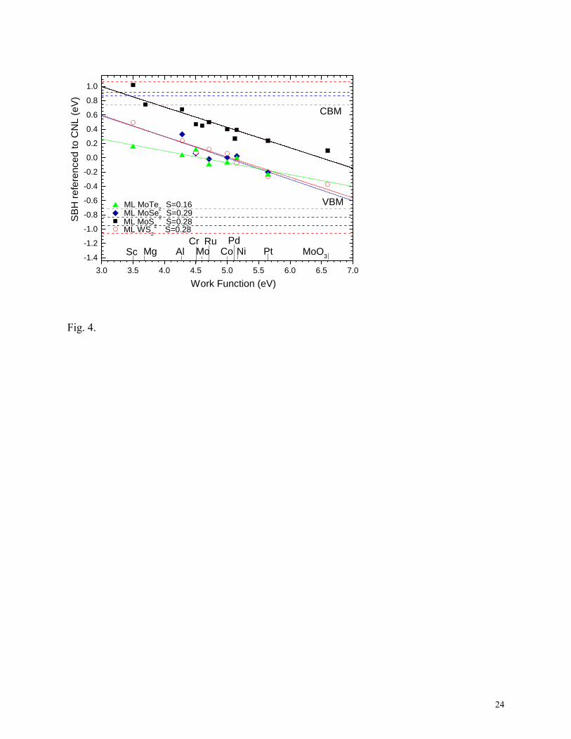
MoSe2, MoTe2 and WS2 to consider the chemical trends. The same range of metals is used. Fig 4
shows the calculated barrier heights. We see that the calculated pinning factors lie in a similar
range. We find that the SBHs on WS2 have a similar trend of SBH values as in MoS2, except that
the SBHs of MoSe2, MoTe2 and WS2 are shifted lower in the gap.
We can derive a fitted value of the CNL for top contact on monolayer MoS2 from Fig 3a as
1.45 eV above the valence band. This assumes an ionization potential (IP) of 5.98 eV for ML
MoS2, derived from the experimental IP of bulk MoS2 of 5.47 from Jaegermann et al48
, allowing
for the VB shift with layer number. The fitted CNL value is within 0.05 eV of the calculated
value in right margin of Fig 3a.
Monch28
noted that the pinning factors of different 3D semiconductors obeyed an empirical
relationship
2)1(1.01
1
S (4)
9
where ε∞ is the optical dielectric constant. The pinning factor for MoTe2 is lower than in MoS2
because of its narrower band gap and larger ε∞ value, according to (4).
Fig. 5 shows that the experimental SBH values of 3D semiconductors follow this dependence
(4) quite well. Taking the optical dielectric constants of TMDs from the literature49
, we can plot
the S versus ε∞ in Fig. 5 according to eq (4). The data points follow relationship (4) reasonably
closely but lie slightly below the 3D line. The slope is quite similar. It is interesting to see that
old experimental data points for the 2D GaS-GaTe series of Kurtin50
have a similar slope to the
3D semiconductors.
The combination of experimental data for 3D semiconductors, our calculated S values for
TMDs, and previous data for the GaS 2D semiconductors suggest that all three families follow a
similar model, the MIGS model. However, for a given ε∞, the (1/S) - 1 value is shifted lower for
the 2D GaS family and the 2D TMDs, corresponding to a lower net density of MIGS (N) in
equation (2).
We now explain why the TMDs tend to follow the MIGS model, despite their two-dimensional
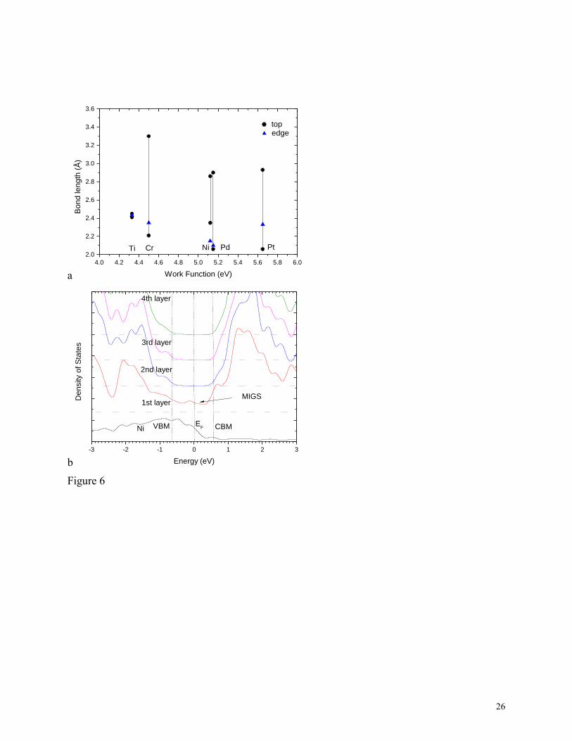
bonding. It is because the top contact metal atoms strongly bond to the TMDs, and the contact
metal to chalcogen bonds are as short as in the edge contacts. The bond lengths between contact
metals and the S sites of MoS2 are shown in Fig 6(a). The intra-layer Mo-S bond length is 2.41Å.
The bond lengths for top contacts cover a range, due to the lower symmetry. For the shortest
distance, the bond length is the same as for the edge contacts, Fig 6(a). Thus, there is mostly
strong bonding between the contact metal atoms and the S atoms. It is not van der Waals
bonding. Interestingly, the presence of top contact bonds does not disrupt the intra-layer M-X
bonds of the MoS2 or WS2 layer, because MoS2 and WS2 are both strongly bonded systems with
a large heat of formation44
, Mo and W being at the center of the transition metal series. The

10
second point is that the chalcogens are third or higher row elements and their atoms can over-
coordinate without affecting the interlayer bonding of MoS2. They are not like C atoms in
graphene. Thus, the pinning factors, the similarity of top and edge contacts, and the contact atom
bond lengths all support the idea that MX2 SBHs follow the standard MIGS model. The MIGS
states themselves can be seen as gap states decaying away from the electrode interface in Fig
6(b).
Experimentally, the preparation of contacts can lead to the creation of defects. These give rise
to extra pinning as seen by the experiments of Das11
and McDonnell18
. The effect of defects on
SBHs in these systems has been studied theoretically by Liu et al43
and Guo et al51
. The different
SBH between top and edge contacts could also introduce a local variation of SBHs and might
also account for the data of McDonnell18
.
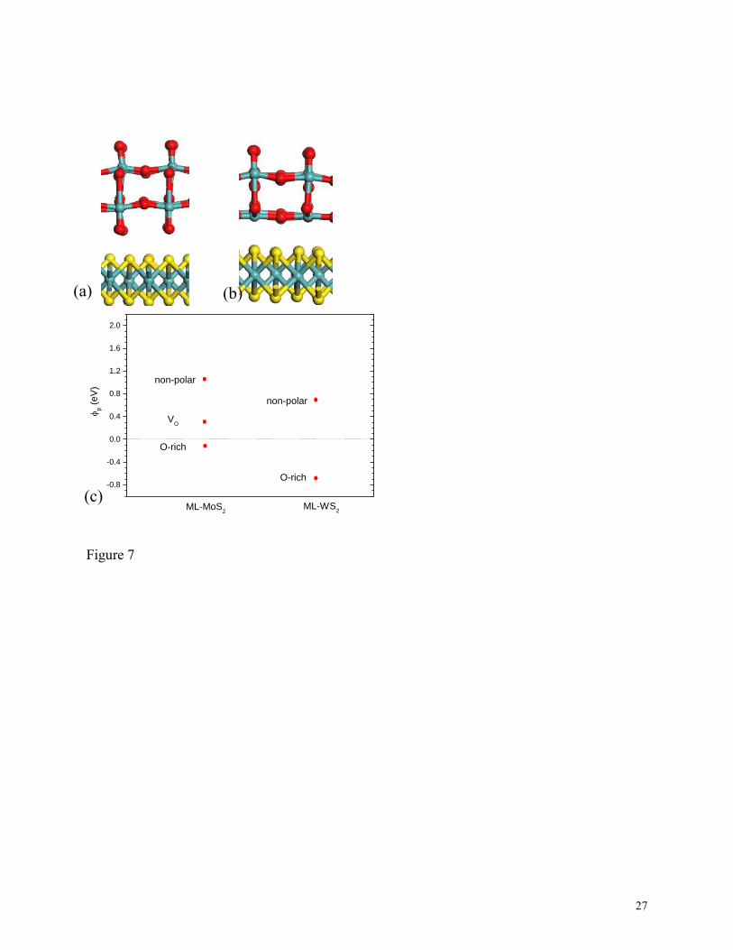
Finally, we considered MoO3/MoS2 contacts for the extremely high work function case. O-
deficient MoO3 is a degenerate n-type semiconductor with a work function of 6.6 eV50
. Fig
7(a,b) shows the O-rich and non-polar MoO3 faces. The non-polar face gives a SBH that falls on
the trend line in Fig 2. The O-rich interface gives a much more p-type SBH, closer to the valence
band, Fig 7c. Thus, MoO3 electrode is a valuable method to give a hole contact, as found by
experiment19
. The introduction of O vacancies, moving from the O rich interface towards the
non-polar interface leads to a large change in SBH.
In summary, the contact problem for 2D TMDs has been studied by detailed DFT calculations.
A strong Fermi level pinning effect is found for all defect-free metal:TMD interfaces. The
calculated Schottky barrier heights follow the standard MIGS model, despite van der Waals
inter-layer bonding. The strong pinning occurs because the contact metal atoms are quite
strongly bonded to the S atoms of MoS2, even for top contacts, while not disturbing the intra-

11
layer Mo-S bonding. The Fermi level is pinned near the conduction band for MoS2 and nearer
midgap for other 2D TMDs. The pinning factor is 0.3 for MoS2 and is lower for other 2D
materials. This explains why most MoS2 MOSFETs are n-type. Defects increase the pinning, and
reduce the dependence of SBH on contact metal work function even further, and shift the pinning
energy towards the anion vacancy defect level.
The authors acknowledge the financial support of EPSRC grant EP/J011592.

12
References
1. Mak, K. F.; Lee C.; Hone, J.; Shan, J.; and Heinz, T. F. Atomically Thin MoS2: A New
Direct-Gap Semiconductor. Phys. Rev. Lett. 2010, 105, 136805.
2. Radisavljevic, B.; Radenovic, A.; Brivio, J.; Giacometti, V.; Kis, A. Single-layer MoS2
transistors. Nat. Nanotechnol. 2011, 6, 147-150.
3. Butler, S. Z.; Hollen, S. M.; Cao, L.; Cui, Y.; Gupta, J. A.; Gutiérrez, H. R.; Heinz, T. F.;
Hong, S. S.; Huang, J.; Ismach, A. F.; et al. Progress, Challenges, and Opportunities in Two-
Dimensional Materials Beyond Graphene. ACS Nano 2013, 7, 2898–2926.
4. Yoon, Y.; Ganapathi, K.; Salahuddin, S. How Good Can Monolayer MoS2 Transistors
Be? Nano Lett. 2011, 11, 3768–3773.
5. Das, S.; Prakash, A.; Salazar, R.; Appenzeller, J. Toward Low-Power Electronics:
Tunneling Phenomena in Transition Metal Dichalcogenides. ACS Nano 2014, 8 1681-1689.
6. Fiori, G.; Bonaccorso, F.; Iannaccone, G.; Palacios, T.; Neumaier, T.; Seabaugh, A.;
Banerjee, S.K.; Colombo, L.; Electronics based on two-dimensional materials. Nat. Nanotechnol.
9 768 (2014)
7. Kim, S.; Konar, A.; Hwang, W.; Lee, J.; Lee, J.; Yang, J.; Jung, C.; Kim, H.; Yoo, J.;
Choi, J.; Jin, Y.; et al. High-mobility and low-power thin-film transistors based on multilayer
MoS2 crystals. Nat. Commun. 2012, 3, 1011.
8. Wu, W.; De, D.; Chang, S.C.; Wang, Y.N.; Peng, H.B.; Bao, J.M.; Pei, S.S. High
mobility and high on/off ratio field-effect transistors based on chemical vapor deposited single-
crystal MoS2 grains. Appl. Phys. Lett. 102 142106 (2013).
13
9. Zhang, Y. J.; Ye, J. T.; Matsuhashi, Y. and Iwasa Y. Ambipolar MoS2 Thin Flake
Transistors. Nano. Lett. 2012, 12, 1136-1140.
10. Liu, H.; Neal, A. T.; Ye, P. D.; Channel Length Scaling of MoS2 MOSFETs. ACS Nano
2012, 6 8563-8569.
11. Das, S.; Chen, H. Y.; Penumatcha, A. V. and Appenzeller J., High Performance
Multilayer MoS2 Transistors with Scandium Contacts. Nano. Lett. 2013, 13, 100-105.
12. Pradhan, N. R.; Rhodes, D.; Zhang, Q.; Talapatra, S.; Terrones, M.; Ajayan, P. M.;
Balicase, L. Intrinsic carrier mobility of multi-layered MoS2 field-effect transistors on SiO2.
Appl. Phys. Lett. 2013, 102, 123105.
13. Bao, W.;Cai, X.; Kim, D.; Sidhara, K.; Fuhrer, M. S. High mobility ambipolar MoS2
field-effect transistors: Substrate and dielectric effects. Appl. Phys. Lett. 2013, 102, 042104.
14. Das, S.; Appenzeller, J. WSe2 field effect transistors with enhanced ambipolar
characteristics. Appl. Phys. Lett. 2013, 103, 103501.
15. Liu, W.; Kang, J. H.; Sarkar, D.; Khatami, Y.; Jena, D. and Banerjee, K. Role of Metal
Contacts in Designing High-Performance Monolayer n-Type WSe2 Field Effect Transistors.
Nano. Lett. 2013, 13, 1983-1990.
16. Zhang, W.; Chiu, M.; Chen, C.-H.; Chen, W.; Li, L.-J.; Wee, A. T. S. Role of Metal
Contacts in High-Performance Phototransistors Based on WSe2 Monolayers. ACS Nano, 2014, 8,
8653.

14
17. Lince, J. R.; Carre, D. J.; Fleischauer, P. D. Schottky-Barrier Formation on a Covalent
Semiconductor without Fermi-Level Pinning: The Metal-MoS2(0001) Interface. Phys. Rev. B
1987, 36, 1647.
18. McDonnell, S.; Addou, R.; Buie , C.; Wallace, R. M.; Hinkle, C L. Defect-Dominated
Doping and Contact Resistance in MoS2. ACS Nano, 2014, 8, 2880–2888.
19. Chuang, S.; Battaglia, C.; Azcatl, A.; McDonnell, S.; Kang, J. S.; Yin, X.; Tosun, M.;
Kapadia, R.; Fang, H.; Wallace, R. M.; Javey, A.; MoS2 P-type Transistors and Diodes Enabled
by High Work Function MoOx Contacts. Nano Lett. 2014, 14, 1337-1342.
20. McDonnell, S.; Azcatl, A.; Addou, R.; Gong, C.; Battaglia, C.; Chuang, S.; Cho, K.J.;
Javey, A.; Wallace, R.M.; ACS Nano 8 6265 (2014)
21. Popov, I.; Seifert, G.; Tomanek, D. Designing Electrical Contacts to MoS2 Monolayers:
A Computational Study. Phys. Rev. Lett. 2012, 108, 156802.
22. Gong, C.; Colombo, L.; Wallace, R M.; Cho, K. J. The Unusual Mechanism of Partial
Fermi Level Pinning at Metal–MoS2 Interfaces. Nano Lett., 2014, 14, 1714-1720.
23. Chen, W.; Santos, E. J. G.; Zhu, W. G.; Kaxiras, E.; Zhang, Z. Y. Tuning the Electronic
and Chemical Properties of Monolayer MoS2 Adsorbed on Transition Metal Substrates. Nano
Lett. 2013, 13, 509-514.
24. Cakir, D.; Peeters, F. M.; Dependence of the electronic and transport properties of metal-
MoSe2 interfaces on contact structures. Phys. Rev. B 2014, 89, 245403.

15
25. Kang, J.; Liu, W.; Sarkar, D.; Jena, D.; Banerjee, K.; Computational Study of Metal
Contacts to Monolayer Transition-Metal Dichalcogenide Semiconductors. Phys. Rev. X 2014, 4,
031005.
26. Y Guo, J Robertson, Schottky barrier heights and band alignments in transition metal
dichalcogenides. Microelec. Eng. 2015, 147, 184-187.
27. Tersoff, J. Schottky Barrier Heights and the Continuum of Gap States. Phys. Rev. Lett. 1984,
52, 465.
28. Mönch, W. Role of Virtual Gap States and Defects in Metal-Semiconductor Contacts. Phys.
Rev. Lett. 1987, 58, 1260.
29. Mönch, W. Metal-Semiconductor Contacts: Electronic Properties. Surf. Sci. 1994, 300, 928-
944.
30. Robertson, J. Band Offsets of Wide-Band-Gap Oxides and Implications for Future
Electronic Eevices. J. Vac. Sci. Technol. B 2000, 18, 1785-1791.
31. Robertson, J. Band offsets, Schottky barrier heights, and their effects on electronic
devices. J. Vac. Sci. Technol. A 2013, 31, 050821.
32. Ellis, J. K.; Lucero, M J.; Scuseria, G. E.; The Indirect to Direct Band Gap Transition in
Multilayered MoS2 as Predicted by Screened Hybrid Density Functional Theory. Appl. Phys.
Lett. 2011, 99, 261908.
33. Lang, N.D.; Kohn, W. Theory of Metal Surfaces: Work Function. Phys. Rev. B 1971,3,
1215.
16
34. Clark, S. J.; Segall, M. D.; Pickard, C. J.; Hasnip, P. J.; Probert, M. J.; Refson, K., Payne,
M. C. First principles methods using CASTEP. Zeitschrift für Kristallographie - Crystalline
Materials. 2005, 220, 567-570.
35. Grimme, S. Semiempirical GGA-type density functional constructed with a long-range
dispersion correction. J. Comp. Chem. 2006, 27, 1787-1799.
36. McNellis, E. R.; Meyer, J.; Reuter, K. Azobenzene at coinage metal surfaces: Role of
dispersive van der Waals interactions. Phys. Rev. B 2009, 80 205414.
37. Clark, S.J.; Robertson, J Screened Exchange Density Functional Applied to Solids. Phys.
Rev. B 2010, 82, 085208.
38. Cheiwchanchamnangij, T.;Lambrecht, W. R. L. Quasiparticle band structure calculation
of monolayer, bilayer, and bulk MoS2. Phys. Rev. B 2012, 85, 205302.
39. Ramasubramaniam, A. Large Excitonic Effects in Monolayers of Molybdenum and
Tungsten Dichalcogenides. Phys. Rev. B 2012, 86, 115409.
40. Kraut, E. A.; Grant, R. W.; Waldrop, J. R.; Kowalczyk, S. P. Precise Determination of
the Valence-Band Edge in X-Ray Photoemission Spectra: Application to Measurement of
Semiconductor Interface Potentials. Phys. Rev. Lett. 1980, 44,1620.
41. Michaelson, H.B. The Work Function of the Elements and Its Periodicity. J. Appl. Phys.
1977, 48, 4729.
42. Cowley, A. W.; Sze, S. M.; Surface States and Barrier Height of Metal‐Semiconductor
Systems. J. Appl. Phys. 1965, 36, 3212.
17
43. Liu, D.; Guo, Y.; Fang, L.; Robertson, J. Sulfur Vacancies in Monolayer MoS2 and Its
Electrical Contacts. Appl. Phys. Lett. 2013, 103, 183113.
44. Guo, Y.; Liu, D.; Robertson, J. Chalcogen vacancies in monolayer transition metal
dichalcogenides and Fermi level pinning at contacts. Appl. Phys. Lett. 2015, 106, 173106.
45. C. Gong, S. McDonnell, X. Qin, A. Azcati, H. Dong, Y.J. Chabal, K.J. Cho, R. M.
Wallace, ACS Nano 8, 642 (2014).
46. Tse, K.Y.; Robertson, J. Control of Schottky Barrier Heights on High-K Gate Dielectrics
for Future Complementary Metal-Oxide Semiconductor Devices. Phys. Rev. Lett. 2006, 99,
086805.
47. Yue, Q.; Shao, Z.; Zhang, X.; Chang, S.; Wang G.; Qin, Q.; Li, J.; Mechnaical and
electronic properties of monolayer MoS under elastic strain. Phys. Lett. A 2012, 376,1166-1170.
48. Schlaf, R.; Lang, O.; Pettenkofer, C.; and Jaegermann, W.; Band Lineup of Layered
Semiconductor Heterostructures prepared by Van der Waals Epitaxy, J Appl Phys 1999, 85,
2732.
49. Bell, M. G.; Liang, W. Y. Electron energy loss studies in solids; The transition metal
dichalcogenides. Adv. Phys. 1976, 25, 53-86;
50. Kurtin, S.; Mead, C. A. Surface Barriers on Layer Semiconductors: GaS, GaSe, GaTe. J.
Phys. Chem. Solids 1969, 30, 2007.
51. Guo, Y.; Robertson, J. Origin of the high work function and high conductivity of MoO3
Appl. Phys. Lett. 2014, 105, 222110.

18
Table 1 Comparison of band gaps calculated by GGA and SX, and the isotropically averaged
CNL values calculated from the SX bands.
eV Band gap
Isotropic
CNL
GGA SX calculated
MoS2-ML 1.55 1.88 0.95
MoSe2-ML 1.53 1.71 0.84
MoTe2-ML 1.38 1.46 0.72
WS2-ML 1.94 2.13 1.07
WSe2-ML 1.64 1.82 0.73
WTe2-ML 1.55 1.31 0.63
MoS2-3D 0.97 1.3 0.70
MoSe2-3D 0.95 1.16 0.43
MoTe2-3D 0.78 1.01 0.33
WS2-3D 1.17 1.44 0.88
WSe2-3D 1.15 1.33 0.77
WTe2-3D 1.01 1.07 0.39

19
Figure captions
1 Bonding at (a) Ti-MoS2, (b) Cr –MoS2, (c) Ni-MoS2 top contacts. Mo= cyan, S= yellow, metal
blue/grey. Edge metal-MoS2 contacts, top views. (d) non-polar armchair, (e) S-terminated
zigzag, (f) and Mo terminated zigzag. Mo=cyan, S = yellow, metal =purple.
2. Comparison of calculated Schottky barrier heights for top contacts on bulk and monolayer
MoS2 in GGA, referenced to their charge neutrality levels. Monolayer data and band edges = red,
bulk data and band edges = black.
3(a) Calculated p-type SBHs for the three edge-contacted ML MoS2 interface, compared to the
case of top-contacted ML MoS2, referenced to valence band maximum. Note the similar pinning
factors S for each case. (b) Calculated Mo d density of states separated into angular components,
showing the different contributions to the bands.
4. Comparison of calculated p-type barrier heights for monolayer MoS2, MoSe2, MoTe2 and
WS2 refered to their CNLs. Colors of data points, fit, and band edges for each compound.
5. Experimental values of pinning factors S for 3D semiconductors, for the 2D series GaS, GaSe
and GaTe ref 49), and our calculated values of pinning factors for bulk MoS2, MoSe2, MoTe2
and WS2 plotted against optical dielectric constant.
6. (a) Comparison of contact metal – S bond lengths for top and edge contacts for various metals
on MoS2. (b) Partial density of states at MoS2 layers away from a Ni/MoS2 interface, showing
the decay of the metal induced gap states.
7 (a,b) MoO3 O-rich and non-polar interfaces with MoS2. O=red, Mo=cyan, S= yellow. (c)
Calculated Schottky barrier heights for O-rich and non-polar MoO3 faces on monolayer MoS2

20
and WS2, referred to VB edge. For MoS2 we have also included the O-rich surface with O
vacancy defect at the MoO3 interface, labeled as VO.
21
a
b
c
d
e
f
Fig. 1.
22
3.0 3.5 4.0 4.5 5.0 5.5 6.0 6.5 7.0
-1.2
-1.0
-0.8
-0.6
-0.4
-0.2
0.0
0.2
0.4
0.6
0.8
1.0
1.2
1.4
1.6
CBM
MoPd
MoO3Sc
SB
H r
efe
ren
ce
d to
CN
L (
eV
)
Work Function (eV)
Bulk S=0.33
Monolayer S=0.28
AlCr Ru
Co Ni Pt
VBM
Mg Ti
Figure 2
23
a3.5 4.0 4.5 5.0 5.5 6.0 6.5 7.0
0.0
0.2
0.4
0.6
0.8
1.0
1.2
1.4
1.6
1.8
2.0
Top S=0.28
Armchair S=0.29
Zigzag S-edge S=0.24
Zigzag Mo-edge S=0.27
Mo
PdMoO
3Sc AlCr Ru
Co Ni Pt
Work Function (eV)
p (
eV
)
CBM
Top
CNL
edge
CNL
b -4 -3 -2 -1 0 1 2 3 4
S pz
S px+p
y
CBMPD
OS
Mo dx
2-y
2+dxy
Mo dzy
+dzx
Mo dz
2
VBM EF
Figure 3
24
3.0 3.5 4.0 4.5 5.0 5.5 6.0 6.5 7.0
-1.4
-1.2
-1.0
-0.8
-0.6
-0.4
-0.2
0.0
0.2
0.4
0.6
0.8
1.0
VBM
SB
H r
efe
ren
ce
d to
CN
L (
eV
)
Work Function (eV)
MoPd
MoO3
Sc AlCr Ru
Co Ni PtMg
CBM
ML MoTe2 S=0.16
ML MoSe2 S=0.29
ML MoS2 S=0.28
ML WS2 S=0.28
Fig. 4.
25
1 100.1
1
10
MoSe2
GaS
GaSe
1
/S -
1
-1
2 3 5 20 30
Xe
LiFBaF
2
SiO2
Al2O
3
ZnS
ZnO
SnO2
SrTiO3
CdS
diamond
CdTe
SiGe
GaAs
GaP
GaTeMoTe
2
WS2
MoS2
3
0.3
Fig. 5
26
a
4.0 4.2 4.4 4.6 4.8 5.0 5.2 5.4 5.6 5.8 6.0
2.0
2.2
2.4
2.6
2.8
3.0
3.2
3.4
3.6
Pd
Bo
nd
le
ng
th (
Å)
Work Function (eV)
Cr Ni
topedge
PtTi
b
-3 -2 -1 0 1 2 3
VBM CBM
4th layer
3rd layer
2nd layer
De
nsity o
f S
tate
s
Energy (eV)
EFNi
1st layerMIGS
Figure 6
27
-0.8
-0.4
0.0
0.4
0.8
1.2
1.6
2.0
O-rich
O-rich
non-polar
ML-WS2
p (
eV
)
ML-MoS2
non-polar
VO
Figure 7
(a) (b)
(c)


