
DRV8304(3-Phase Gate
Driver)
MSP430FR5949
TPS709
3.3V
LDO
Position Feedback
CSD87502Q2 (x3)
DRV5013
10.8 V (DC Supply)
TVS3300
TIDA-01587
BLDC Motor
+
-
Copyright © 2018, Texas Instruments Incorporated
1TIDUE42–February 2018Submit Documentation Feedback
Copyright © 2018, Texas Instruments Incorporated
10.8-V/30-W, >95% Efficiency, 4.3-cm2, Power Stage Reference Design forBrushless DC Servo Drive
TI Designs: TIDA-0158710.8-V/30-W, >95% Efficiency, 4.3-cm2, Power StageReference Design for Brushless DC Servo Drive
DescriptionThis 15-W, 16-mm × 27-mm, power stage referencedesign drives and controls the position of thebrushless DC (BLDC) motor operating from a three- tofour-cell Li-ion battery. This highly-efficient solution isoptimized with a very small form factor that easily fitsinto the motor and supports precise motor positioncontrol. The design is also capable of driving the motorat high speeds with position feedback. The referencedesign is protected for overcurrent and short circuit,and the onboard MCU provides UART connectivity,which enables controllability with any externalcontroller.
Resources
TIDA-01587 Design FolderDRV8304 Product FolderCSD87502Q2 Product FolderMSP430FR5949 Product FolderTPS709 Product FolderTVS3300 Product Folder
ASK Our E2E™ Experts
Features• BLDC Servo Drive Operates at Voltage Ranging
from 6-V to 16.8-V (Three- to Four-Cell Li-ionBattery)
• Supports 2.5-ARMS Continuous, 5-A Peak MotorWinding Current
• Supports Trapezoidal and Sinusoidal Control forPermanent Magnet Motors
• Closed Loop 60° Electrical Position Control WithDigital Hall Sensor Feedback for BLDC Motor
• Supports Position Control with SinusoidalExcitation with Analog Hall Feedback
• Very Small PCB Form Factor of 16 mm × 27 mm• Power Stage Efficiency > 95%, Without Heat Sink• Increased Battery Life With High-Efficiency Power
Stage, Low-Power MCU, and Low-QuiescentCurrent LDO
• Overcurrent, Shoot-Through, and UndervoltageProtection
• Provision for UART Wired Communication• Operating Ambient Temperature: –20°C to +55°C
Applications• Humanoids• Vacuum Robots• Robotic Lawn Mowers
An IMPORTANT NOTICE at the end of this TI reference design addresses authorized use, intellectual property matters and otherimportant disclaimers and information.

High end motors used in leg, neck and arm shoulder of the robot
Low end motor used in other positions
System Description www.ti.com
2 TIDUE42–February 2018Submit Documentation Feedback
Copyright © 2018, Texas Instruments Incorporated
10.8-V/30-W, >95% Efficiency, 4.3-cm2, Power Stage Reference Design forBrushless DC Servo Drive
1 System DescriptionA humanoid robot is a type of service robot used in wide-end applications such as research applicationswhere human access is risky, high-end toys used for teaching, dancing, and speaking, and more. Multiplemotors are present in a typical humanoid depending upon the features and application requirement. Thecommonly used motors are brushed DC (BDC), brushless DC (BLDC), and sometimes stepper types.Figure 1 shows the examples of motor drive locations in a typical humanoid. The high-end or high-powermotors are typically present in the neck, legs, shoulders, and so on. Low-end or low-power motors areused in other locations such as elbows, knees, fingers, and so on. The electronic drive used in thesemotors has the following requirements:• Must be small enough to fit with the motor• Must support accurate position and torque control• Must have the sufficient holding torque capability
Figure 1. Typical Humanoid—Motor Drive Locations
Vacuum robots are another service robot widely used in consumer applications for cleaning. The motorsused in vacuum robots have different requirements like high-speed rotation, high torque-slow speedoperation, or position control depending on the functionality these motors support (for example, suction,wheel, side brush, position control of the robotic vision control motor, and so on). BDC, BLDC, or steppermotors are typically used. The electronic drives have similar requirements as said in the case ofhumanoids.
This three-phase BLDC power stage reference design can support the position control in a humanoid orthe motor control in a vacuum robot. The design demonstrates the BLDC motor servo drive power stage ina very small form factor using the highly-integrated three-phase gate driver DRV8304 featuring a highlevel of integration and protection, reducing the overall BOM to a large extend.

www.ti.com System Description
3TIDUE42–February 2018Submit Documentation Feedback
Copyright © 2018, Texas Instruments Incorporated
10.8-V/30-W, >95% Efficiency, 4.3-cm2, Power Stage Reference Design forBrushless DC Servo Drive
The very small form factor and higher efficiency is also achieved by using the CSD87502Q2 offering twoindependent 30-V N-channel MOSFET in a SON 2×2 mm plastic package, having a low drain-to-sourceon-resistance (RDS(on)) of 27 mΩ. The TPS709 LDO features a low-quiescent current (< 1 μA) andgenerates the low-noise, stable, 3.3-V power supply for the MCU. The MSP430FR5949 runs the positioncontrol algorithm by taking the position feedback signals from the motor, and offers trapezoidal andsinusoidal motor control. The TVS3300 provide surge voltage protection on input voltage supply.
The test report evaluates the board power capability, efficiency, overcurrent protection, peak currentcapability, and the position control with sufficient hold-up torque.
1.1 Key System Specifications
Table 1. Key System Specifications
PARAMETERS SPECIFICATIONSInput voltage 10.8-V DC (6-V minimum to 16.8-V maximum)Rated output power 30 WRMS winding current 2.5 APeak winding current 5 AInverter switching frequency 20 kHz (adjustable from 5 kHz to 100 kHz)
Feedback signals DC bus voltage, analog or digital position feedback, low-sideinverter leg currents
Protections Overcurrent, input undervoltage, over temperature, shoot-through
Cooling Natural cooling only, no heat sinkOperating ambient –20°C to +55°CBoard specification 16 mm × 27 mm, 2-layer, 1-oz copper, 1.6-mm board thicknessEfficiency > 95%

DRV8304(3-Phase Gate
Driver)
MSP430FR5949
TPS709
3.3V
LDO
Position Feedback
CSD87502Q2 (x3)
DRV5013
10.8 V (DC Supply)
TVS3300
TIDA-01587
BLDC Motor
+
-
Copyright © 2018, Texas Instruments Incorporated
System Overview www.ti.com
4 TIDUE42–February 2018Submit Documentation Feedback
Copyright © 2018, Texas Instruments Incorporated
10.8-V/30-W, >95% Efficiency, 4.3-cm2, Power Stage Reference Design forBrushless DC Servo Drive
2 System Overview
2.1 Block Diagram
Figure 2. TIDA-01587 Block Diagram
2.2 Highlighted Products
2.2.1 DRV8304The key requirements in selecting the gate driver are:• Small form factor, three-phase gate driver with high level of integration and protection• Support the operating voltage range with sufficient gate current• Support the required minimum DC input voltage, still provides sufficient gate voltage for the external
FET to operate at the minimum RDS(on)
• Low power consumption
The reference design uses the three-phase gate driver DRV8304, which is specified for 6 V to 38 V,providing a maximum gate current of 150-mA source and 300-mA sink. The DRV8304 can supportapplications including field-oriented control (FOC), sinusoidal current control, and trapezoidal currentcontrol of BLDC motors. The DRV8304 device integrates three current-sense amplifiers (CSA) for sensingthe phase currents of BLDC motors for optimum FOC and current-control system implementation. AnAUTOCAL feature automatically calibrates the CSA offset error for accurate current sensing.
The DRV8304 device is based on smart gate-drive (SGD) architecture to eliminate the need of anyexternal gate components (resistors and Zener diodes) while fully protecting the external FETs. The SGDarchitecture optimizes dead time to avoid any shoot-through conditions, provides flexibility in reducingelectromagnetic interference (EMI) by gate slew-rate control and protects against any gate-shortconditions. Strong pulldown current also prevent any dv/dt gate turnon. The gate driver provideovercurrent and short-circuit protection by MOSFET VDS monitoring.

www.ti.com System Overview
5TIDUE42–February 2018Submit Documentation Feedback
Copyright © 2018, Texas Instruments Incorporated
10.8-V/30-W, >95% Efficiency, 4.3-cm2, Power Stage Reference Design forBrushless DC Servo Drive
2.2.2 CSD87502Q2The key requirements in selecting the power stage MOSFETs are:• Low RDS(on) and gate charge for high efficiency operation• Small form factor• Low thermal resistance and provision for heat dissipation to PCB
The reference design uses the CSD87502Q2, which is a 30-V, 27-mΩ N-channel device with dualindependent MOSFETs in a SON 2×2-mm plastic package. The dual FETs feature a low RDS(on) thatminimizes losses and offers low component count for space-constrained applications. The low junction-to-ambient thermal resistance with the help of thermal pads on the package allows easy heat dissipation.
2.2.3 MSP430FR5949The MSP430™ ultra-low-power (ULP) FRAM platform combines uniquely embedded FRAM and a holisticultra-low-power system architecture, allowing innovators to increase performance at lowered energybudgets. FRAM technology combines the speed, flexibility, and endurance of SRAM with the stability andreliability of flash at much lower power.
The MSP430 ULP FRAM portfolio consists of a diverse set of devices featuring FRAM, the ULP 16-bitMSP430 CPU, and intelligent peripherals targeted for various applications. The ULP architectureshowcases seven low-power modes, optimized to achieve extended battery life in energy-challengedapplications.
The device has a 16-bit RISC architecture supporting up to a 16-MHz clock. The device has five 16-bittimers with up to seven capture/compare registers each. The seven capture/compare registers helps torealize six PWM signals for three-phase sine control with a single time base. The device has 32-bithardware multiplier and a 12-bit analog-to-digital converter (ADC) with internal reference and sample-and-hold and up to 16 external input channels. The enhanced serial communication allows easycommunication with master controller in different service robots.
2.2.4 TPS709The TPS70933 linear regulator is an ultra-low, quiescent current device designed for power-sensitiveapplications. The LDO can work up to a 30-V input voltage, which makes it ideal for up to six-cell Li-ionbattery supply application. A precision band-gap and error amplifier provides 2% accuracy overtemperature. A quiescent current of only 1 μA makes this LDO ideal for battery-powered, always-onsystems that require very little idle-state power dissipation. This device has thermal-shutdown, currentlimit, and reverse-current protections for added safety. The TPS70933 linear regulator is available inWSON-6 and SOT-23-5 packages.
2.2.5 TVS3300The TVS3300 is a transient voltage suppressor that provides robust protection for electronic circuitsexposed to high transient voltage events. Unlike a traditional TVS diode, the TVS3300 precision clamptriggers at a lower breakdown voltage and regulates to maintain a flat clamping voltage throughout atransient overvoltage event. The lower clamping voltage combined with a low dynamic resistance enablesa unique TVS protection solution that can lower the voltage a system is exposed during a surge event byup to 30% in unidirectional configuration and up to 20% in bidirectional configuration when compared totraditional TVS diodes.
The TVS3300 is a unidirectional precision surge protection clamp with a 33-V working voltage designedspecifically to protect systems with mid-voltage rails in industrial, communication, and factory automationapplications. The TVS3300 has a fast response time when surge current is applied so there is noovershoot voltage during clamping, making it ideal to replace traditional TVS and Zener diodes.
The TVS3300 is available in two small footprint packages which, when used in place of an industrystandard SMB package, can reduce footprint by 94% (WCSP package) and 79% (SON package) forspace constrained applications. Both package options robustly dissipate the surge power and provide upto 58% lower leakage current compared to traditional TVS diodes in SMA and SMB package.

7
2
1
6
Q1A
CSD87502Q2
5
4
3 8
Q3B
CSD87502Q2
0.006
R8
0.006
R6
0.006
R7
GHB GHC
SHB SHC
GLCGLB
SPA SPB SPC
GND GND GND
GHA
SHA
GLA 5
4
3 8
Q1B
CSD87502Q2
7
2
1
6
Q3A
CSD87502Q25
4
3 8
Q2B
CSD87502Q2
7
2
1
6
Q2A
CSD87502Q2
VM
SNA SNB SNC
Copyright © 2018, Texas Instruments Incorporated
max max
DC ADC _DC
619 k 2000 k 619 k 2000 k3.3 13.96 V
619 k 619 kV V: : : :
u u : :
VM
2.0M
R1
GND
619k
R4
DC_BUS
GND
VMIN
4
IN5
GND1
GND2
IN6
GND3
PAD7
U5
TVS3300DRVR
GND
VM
0.1µFC3
GND
1
2
J5
Copyright © 2018, Texas Instruments Incorporated
System Overview www.ti.com
6 TIDUE42–February 2018Submit Documentation Feedback
Copyright © 2018, Texas Instruments Incorporated
10.8-V/30-W, >95% Efficiency, 4.3-cm2, Power Stage Reference Design forBrushless DC Servo Drive
2.3 System Design Theory
2.3.1 DC Voltage Input to the BoardThe board gets the DC input voltage through the jumper J5 as shown in Figure 3. The TVS3300 is a surgeprotection clamp provided at the input to protect the circuit from input voltage surges. The design isoptimized for a three-cell Li-ion battery and can support up to four-cell applications, having a maximumvoltage of 16.8 V.
Figure 3. Schematic of Battery Power Input Section
The input supply voltage PVDD is scaled using the resistive divider network, which consists of R1, R4,and C3, and fed to the MCU. Considering the maximum voltage for the MCU ADC input as 3.3 V, themaximum DC input voltage measurable by the MCU is calculated as in Equation 1.
(1)
Considering a 10% headroom for this value, the maximum recommended voltage input to the system is13.96 × 0.9 = 12.56 V. So for a power stage operating from three-cell Li-ion, having a maximum operatingvoltage of 12.6 V, this voltage feedback resistor divider is ideal. Also, this choice gives optimal ADCresolution for a system operating from 6 V to 12.6 V.
2.3.2 Power Stage Design: Three-Phase InverterThe three-phase inverter is realized using three dual MOSFET blocks CSD87502Q2, as shown inFigure 4. Each CSD87502Q2 block consists of two independent 30-V, 27-mΩ N-channel MOSFETs in aSON 2×2-mm plastic package.
Figure 4. Schematic of Three-Phase Inverter
2 2RMS SENSEPower loss in the resistor I R 2.5 0.006 0.0375 W u u
www.ti.com System Overview
7TIDUE42–February 2018Submit Documentation Feedback
Copyright © 2018, Texas Instruments Incorporated
10.8-V/30-W, >95% Efficiency, 4.3-cm2, Power Stage Reference Design forBrushless DC Servo Drive
The resistors R6, R7, and R8 are used for inverter leg current sensing. The voltage across the senseresistor is fed to the MCU through the current shunt amplifiers in the DRV8304.
2.3.3 Selecting the Sense ResistorThe selection of sense resistor depends on different factors as follows:• Power dissipation in the sense resistor• Offset error voltage and gain of the current sense amplifier• Peak current to be sensed
The sense resistors are designed to carry a continuous nominal RMS current of 2.5 A and a peak currentof 5 A. A high sense resistance value increases the power loss in the resistors. A low sense resistor valueincreases the error due to input offset voltage of the current sense amplifier at high gain. If the current-sense amplifier is used without offset calibration, select the sense resistor value such that the sensevoltage across the resistor is sufficiently higher than the op-amp input offset voltage to reduce the effect ofthe offset error. The TLV9061 has a maximum input offset error voltage of 1.5 mV. The reference designuses a 0.006-Ω sense resistor, and the power loss in sense resistor can be calculated using Equation 2:
(2)
At a 5-A peak current, using Equation 2, the power loss in the resistor = 0.15 W.
2.3.4 Power Stage Design: Three-Phase Gate DriverFigure 5 shows the schematic of the DRV8304 gate driver. C17 is the DVDD decoupling capacitor thatmust be placed close to DRV8304. C6 and C7 are the charge pump capacitors. These capacitors areselected to provide a stable charge pump voltage with minimum ripple. VM is the DC supply input; in thiscase, it is the battery voltage of 10.8 V. C1 and C4 are the bulk ceramic capacitor placed near the inverterbridge.
The gate drive circuit is designed, and the different resistors are selected to meet the specification as perTable 2.
Table 2. Design Specification of DRV8304 Gate Driver
PARAMETER DEFAULT VALUE CIRCUIT DESCRIPTIONMODE (PWM mode) 6× PWM control mode MODE pin tied to AGNDIDRIVE (gate source and sink current) 15-mA source, 30-mA sink IDRIVE pin tied to AGNDVDS (monitor reference voltage) 0.15 V VDS pin tied to AGNDGAIN (current sense amplifier gain) 40 V/V GAIN pin tied to 3.3 V (DVDD)VREF 3.3 V Support bidirectional current sensingCAL Controllable through MCU Amplifier calibration through MCU

GND
INHA
INLA
INHB
INLB
INHC
INLC
GND
GND
GND
SOC
SOB
SOA
47µFC4
FAULT
1µFC6
0.047 µF
C7
1µF
C17
0.1µFC5
R22
R25
0R263.3V
GHB
SHB
GLB
GHC
SHC
GLC
SPC
SPB
SPA
100
R15
GND
100
R28
GND
100
R24
GND
SOA
SOC SOC_MCU
SOB_MCU
GHA
SHA
GLA
SOB
0R21
3900pF
C15
3900pF
C19
3900pF
C18
0.1µFC10
SOA_MCU
CAL
ENABLE
22µFC1
VDRAIN5
GHA6
SHA7
GHB15
SHB14
GLB13
GLA8
GHC16
SHC17
GLC18
SPC19
SNC20
SPB12
SNB11
SPA9
SNA10
AGND32
PGND40
PAD41
CPL1
CPH2
VCP3
VM4
DVDD33
MODE26
IDRIVE27
VDS28
INHA34
INLA35
INHB36
INLB37
INHC38
INLC39
ENABLE30
GAIN29
FAULT25
CAL31
VREF24
SOC21
SOB22
SOA23
U2
DRV8304HRHAR
GND
3.3V_LDO
0R5GND
GND0R9
3.3V_LDO
0R10
R18GND
3.3V_LDO
VMVM
SNC
SNB
SNA
Copyright © 2018, Texas Instruments Incorporated
System Overview www.ti.com
8 TIDUE42–February 2018Submit Documentation Feedback
Copyright © 2018, Texas Instruments Incorporated
10.8-V/30-W, >95% Efficiency, 4.3-cm2, Power Stage Reference Design forBrushless DC Servo Drive
Figure 5. Schematic of DRV8304 Gate Driver
O3.3 V
V 3.3 V 0.25 V 1.4 V2
§ · ¨ ¸
© ¹
SENSEV SENSE
1.4 VR
A I
u
REFO REF
VV V 0.25 V
2
RSENSE
I
SPx
SNx
+
± R1
R1
R5
R4
R3
R2
R5
R4
R3
R2+
±
1/2
R6SOx
VCC
VREF
0.1 µF
REFX
SENSESENSE
VSO
2ICSA _ GAIN R
u
www.ti.com System Overview
9TIDUE42–February 2018Submit Documentation Feedback
Copyright © 2018, Texas Instruments Incorporated
10.8-V/30-W, >95% Efficiency, 4.3-cm2, Power Stage Reference Design forBrushless DC Servo Drive
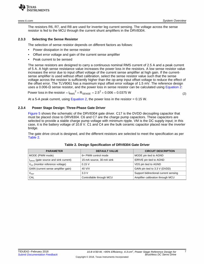
2.3.5 Current Sense AmplifierThe SOx pin on the DRV8304 outputs an analog voltage equal to the voltage seen across the SPx andSNx pin multiplied by the gain setting (CSA_GAIN). The gain setting is adjustable between four differentlevels (5, 10, 20, and 40 V/V). The amplifier as shown in Figure 6 can be used to monitor the currentthrough the half-bridges and the current is approximately calculated using Equation 3.
(3)
Figure 6. DRV8304 Current Sense Amplifier
The sense amplifier gains on the DRV8304 and sense resistor value are selected based on the targetcurrent range, VREF, sense resistor power rating, and temperature. In bidirectional operation of the senseamplifier, the dynamic range at the output is approximately:
where• VREF = 3.3 V (4)
The required current sense range for the reference design is from –5 A to +5 A. The DRV8304 has anSOx output linear range of 0.25 V to VREF – 0.25 V (from the VLINEAR specification). The differential range ofthe sense amplifier input is –0.3 V to +0.3 V (VSP,DIF).
(5)
With RSENSE = 0.006 Ω and an amplifier gain of 40 V/V, using Equation 5, the design allows a currentsensing from –5.8 A to +5.8 A, which means 15% over rated from the required rated peak current of 5 A.

3.3V3.3V
GND
HALL_A_OUT
HALL_B_OUT
GND
0.01µFC11
0.01µFC20
3.3k
R14
3.3k
R11
3.3V
GND
HALL_C_OUT
0.01µFC16
3.3k
R16
1
2
3
J7 3.3V
GND
1.00M
R32
0.1µFC21
POSITION_REF
1
2
3
J4
HALL_A
HALL_B
HALL_C
100R12
100R31
100R17
Copyright © 2018, Texas Instruments Incorporated
P1.0/TA0.1/DMAE0/RTCCLK/A0/C0/VREF-/VEREF-1
P1.1/TA0.2/TA1CLK/COUT/A1/C1/VREF+/VEREF+2
P1.2/TA1.1/TA0CLK/COUT/A2/C23
P3.0/A12/C124
P3.1/A13/C135
P3.2/A14/C146
P3.3/A15/C157
P1.3/TA1.2/UCB0STE/A3/C38
P1.4/TB0.1/UCA0STE/A4/C49
P1.5/TB0.2/UCA0CLK/A5/C510
PJ.0/TDO/TB0OUTH/SMCLK/SRSCG1/C611
PJ.1/TDI/TCLK/MCLK/SRSCG0/C712
PJ.2/TMS/ACLK/SROSCOFF/C813
PJ.3/TCK/SRCPUOFF/C914
P4.0/A815
P4.1/A916
P2.5/TB0.0/UCA1TXD/UCA1SIMO17
P2.6/TB0.1/UCA1RXD/UCA1SOMI18
TEST/SBWTCK19
RST/NMI/SBWTDIO20
P2.0/TB0.6/UCA0TXD/UCA0SIMO/TB0CLK/ACLK21
P2.1/TB0.0/UCA0RXD/UCA0SOMI/TB0.022
P2.2/TB0.2/UCB0CLK23
P3.4/TB0.3/SMCLK24
P3.5/TB0.4/COUT25
P3.6/TB0.526
P3.7/TB0.627
P1.6/TB0.3/UCB0SIMO/UCB0SDA/TA0.028
P1.7/TB0.4/UCB0SOMI/UCB0SCL/TA1.029
P4.4/TB0.530
DVSS31
DVCC32
P2.733
P2.3/TA0.0/UCA1STE/A6/C1034
P2.4/TA1.0/UCA1CLK/A7/C1135
AVSS36
PJ.4/LFXIN37
PJ.5/LFXOUT38
AVSS39
AVCC40
PAD41
U4
MSP430FR5949IRHAR
RXDTXD
TEST
RST
GND
3.3V
GND
4.7µFC12
0.1µFC13
SOA_MCUSOB_MCU
SOC_MCUPOSITION_REF
ENABLE
CAL
HALL_B_OUTHALL_C_OUT
HALL_A_OUT
DC_BUS
INHB
INLCINHCINLB
INLAINHA
GND4.7µFC2
0.1µFC22
3.3V
Copyright © 2018, Texas Instruments Incorporated
System Overview www.ti.com
10 TIDUE42–February 2018Submit Documentation Feedback
Copyright © 2018, Texas Instruments Incorporated
10.8-V/30-W, >95% Efficiency, 4.3-cm2, Power Stage Reference Design forBrushless DC Servo Drive
2.3.6 MSP430FR5949 MCUFigure 7 shows the configuration of MSP430FR5949 MCU. The reference design uses 4.7-µF decouplingcapacitors (C2, C12) at AVCC and DVCC pins. A 0.1-μF capacitor has been added to obtain the bestperformance at a high frequency. The Timer B module of the MCU is used for PWM generation. Theseven capture/compare registers helps to realize six PWM signals for three-phase sine control, with asingle time base. The six PWM signals are generated at TB0.1 to TB0.6 pins. The digital Hall signals areconnected to port 1 of the MCU. For an analog position signal interface, configure the pins as analog pins.The MCU is configured for sensing different analog signals like the inverter leg currents, DC bus voltage,position reference signals, and so on. The provision for UART communication is also provided.
Figure 7. Schematic of MSP430FR5949
2.3.7 Motor Position FeedbackFigure 8 shows the position feedback interface from the motor to the reference design board. By default,the reference design is configured to sense digital Hall sensor output, which is connected to port 1 ofMCU. The reference design can support analog position feedback also; in that case, connect the sensoroutput to same port pins and configure the pins as an analog input pin of the MCU ADC.
The position reference signal can be connected to J7 by connecting an external potentiometer (POT).
Figure 8. Schematic of Position Feedback

DISS IN OUT OUTP V V I u
GND
GND
3.3VVMOUT
1
NC2
GND3
EN4
NC5
IN6
PAD7
U3
TPS70933DRVR
GND
10µFC8
1µFC9
Copyright © 2018, Texas Instruments Incorporated
www.ti.com System Overview
11TIDUE42–February 2018Submit Documentation Feedback
Copyright © 2018, Texas Instruments Incorporated
10.8-V/30-W, >95% Efficiency, 4.3-cm2, Power Stage Reference Design forBrushless DC Servo Drive
2.3.8 LDOThe reference design uses the ultra-low quiescent current, LDO linear regulator TPS70933 to generate the3.3-V power supply for the MCU from the input voltage of 10.8 V. Figure 9 shows the schematic of theLDO circuit.
Figure 9. Schematic of 3.3-V LDO
The selection of LDO depends on the wide input voltage support (in this design, from 6 V to 16.8 V), theload current, and power dissipation. Power dissipation depends on input voltage and load conditions.Power dissipation (PDISS) is equal to the product of the output current and the voltage drop across theoutput pass element, as given in Equation 6.
(6)
Assuming a nominal LDO load current of 20 mA, the power dissipation at VIN = 16.8 V can be calculatedas:
PDISS = (16.8 – 3.3) × 0.02 = 0.27 W
Table 3 shows the specifications of the LDOs used in this reference design. At lower input voltage, thepower dissipation in the LDO reduces. This reference design assumes a maximum LDO output current of30 mA when operating from a three-cell Li-ion battery.
Table 3. Specification of Buck Converter
PARAMETER DESIGN SPECIFICATIONInput voltage 6 V to 16.8 V (10.8-V nominal)Output voltage 3.3 VMaximum output current 30 mA (at 10.8-V input voltage)

J2
GND 3V3HALL_B
HALL_C
Hall Sensor Interface (J4)
HALL_A
3.3 V
Position
GND
Position Reference
(J7)
MSP430TM Programming
Connector (J1)External
Interface (J3)
Tes
t
RS
T
TX
D
RX
D
Fau
lt
Phase C
Phase B
Phase A
DC Voltage Supply Input
(J5)
-
+
Copyright © 2018, Texas Instruments Incorporated
Hardware, Software, Testing Requirements, and Test Results www.ti.com
12 TIDUE42–February 2018Submit Documentation Feedback
Copyright © 2018, Texas Instruments Incorporated
10.8-V/30-W, >95% Efficiency, 4.3-cm2, Power Stage Reference Design forBrushless DC Servo Drive
3 Hardware, Software, Testing Requirements, and Test Results
3.1 Required Hardware and Software
3.1.1 Hardware
3.1.1.1 Connector Configuration of TIDA-01587Figure 10 shows the connector configuration of this reference design, which features:• Two-terminal input for power supply (J5): This pin is used to connect the input DC supply from the
battery. The positive and negative terminals can be identified as shown in Figure 10.• Three-terminal output for motor winding connection: The phase output connections for connecting to
the BLDC motor winding marked as Phase A, Phase B, and Phase C as shown in Figure 10.• Three-pin connector J3: This connector is used for external UART communication interface. The RX
and TX pins enable the communication with external master controller. The FAULT pin of thisconnector gives indication on FAULT signal from gate driver DRV8304.
• Two-pin connector J1: This is the programming connector for the MSP430FR5949 MCU, along with the3.3-V lines at connector J2. The two-wire Spy-Bi-Wire protocol is used to program theMSP430FR5949. See the MSP430FR5949 development tools for programming options with anexternal JTAG interface.
• Three-pin connector J7: This connector interfaces the position reference from external potentiometer. A20k POT can be used.
• Three-pin connector J4: This connector interfaces hall senor position signal from the motor.
Figure 10. PCB Connectors

www.ti.com Hardware, Software, Testing Requirements, and Test Results
13TIDUE42–February 2018Submit Documentation Feedback
Copyright © 2018, Texas Instruments Incorporated
10.8-V/30-W, >95% Efficiency, 4.3-cm2, Power Stage Reference Design forBrushless DC Servo Drive
3.1.1.2 Procedure for Board Bring-up and TestingFollow this procedure for board bring-up and testing:1. Remove the motor connections from the board and power on the input DC supply. Make sure that a
minimum of a 8-V DC input is applied and the 3.3 V is generated in the board.2. Program the MCU. Make sure that the configuration in the program is done as per Section 3.1.2.3. Remove the programmer, and switch off the DC input supply.4. Connect the phase outputs from the board to the motor winding terminals.5. Use a DC power supply with current limit protection and apply 8-V DC to the board. The motor starts
rotating and stops at the position mentioned by the position reference.6. To change direction, switch off the DC input, and correct the logic in the program and re-load the same
in to the MCU.
3.1.2 Software
3.1.2.1 High-Level Description of Application FirmwareThe reference design firmware offers the following features and user controllable parameters:• 60° electrical position control using digital hall sensor position feedback• BLDC motor speed control using trapezoidal control
Table 4 lists the firmware system components.
Table 4. TIDA-01587 Firmware System Components
SYSTEM COMPONENT DESCRIPTIONDevelopment and emulation Code Composer Studio™ (CCS) version 7Target controller MSP430FR5949PWM frequency 20-kHz PWM (default), programmable for higher and lower frequencies
Interrupts Port 1 Interrupts enabled on P1.0, P1.1, and P1.2 corresponds to digital hallsensor interface
PWM generation—Timer configuration PWMs: TB0.1–TB0.6 ; CLOCK = 16 MHz, PWM frequency set for 20 kHz
Position feedback—Hall sensor signalsP1.0 → HALL AP1.1 → HALL BP1.2 → HALL C
ADC channel assignment
A7 → DC bus voltage feedbackA8 → Position reference from potentiometerA13 → Phase C inverter leg currentA14 → Phase A inverter leg currentA15 → Phase B inverter leg current
MCU digital inputs/output and communication
P2.5 → ENABLE signal for DRV8304P2.0 → UART TXDP2.1 → UART RXDP4.1 → CAL pin of DRV8304
3.1.2.2 Customizing the Reference CodeSelect the main.c file. Parameters exist at the top of the file that can be optimized and are included as theconfiguration variables. The following section of code shows these parameters:#define PWM_PERIOD 400 // PWM Frequency (Hz) = 16MHz / ((2*PWM_PERIOD) - 1)#define DUTY_CYCLE 70 // Input Duty Cycle inversely relative to PWM_PERIOD#define POLES 8 // Number of poles in motor#define Gear_Ratio 1 // Gear ratio in the Motor

Mechanical resolution angle from motorEquivalent mechanical position resolution 1.5
Gear ratio q
em
Electrical AngleMechanical Angle
p2
TT
§ ·¨ ¸© ¹
16 MHzPWM Frequency Hz
2 PWM_PERIOD 1
u
Hardware, Software, Testing Requirements, and Test Results www.ti.com
14 TIDUE42–February 2018Submit Documentation Feedback
Copyright © 2018, Texas Instruments Incorporated
10.8-V/30-W, >95% Efficiency, 4.3-cm2, Power Stage Reference Design forBrushless DC Servo Drive
3.1.2.2.1 PWM_PERIODThe PWM_PERIOD parameter sets the value in capture and compare register 0 of Timer_B0. TheTimer_B0 is initialized to operate at a 16-MHz clock. Use Equation 7 to calculate the PWM frequency. TheTIMER_A0 PWM is configured in up-down mode.
(7)
For example, with PWM_PERIOD = 400, PWM frequency ≈ 20 kHz.
3.1.2.2.2 DUTY_CYCLEAdjust this parameter to control the speed of the motor. This parameter is inversely related toPWM_PERIOD.
3.1.2.2.3 POLESThis parameter is the number of magnetic poles in the rotor of motor. The algorithm sets the 60° electricalposition control using BLDC trapezoidal control, which means the resolution accuracy is 60° electrical.
The equivalent mechanical position resolution accuracy can be calculated from the number of magneticpoles in the rotor (p).
(8)
For example, with p = 8, Mechanical resolution angle from motor = 15°. If the motor has a gear with 10:1gear ratio, then:

3.3-V DC output
Ripple in 3.3-V DC output voltageRipple Voltage < 15 mV
24 V, 5 A DCPower Supply
Mechanical Load Connected to Motor
Motor Winding Connections
Hall Sensor Signals
GND 3.3 V-
+
BrushlessDC Motor
Copyright © 2018, Texas Instruments Incorporated
www.ti.com Hardware, Software, Testing Requirements, and Test Results
15TIDUE42–February 2018Submit Documentation Feedback
Copyright © 2018, Texas Instruments Incorporated
10.8-V/30-W, >95% Efficiency, 4.3-cm2, Power Stage Reference Design forBrushless DC Servo Drive
3.2 Testing and Results
3.2.1 Test SetupThe test is performed with a BLDC motor at 10.8-V DC with trapezoidal and sinusoidal control. Figure 11shows the test setup.
Figure 11. Load Test Setup
3.2.2 Test Results
3.2.2.1 3.3-V Power Supply Generated by the LDOFigure 12 shows the 3.3 V generated from the LDO. The ripple in the 3.3-V rail is less than 15 mV.
Figure 12. 3.3 V Generated by TPS70933
3.2.2.2 DRV8304 Gate Driver Output VoltageFigure 13 shows the high-side and low-side gate drive output voltage of DRV8304 at a DC bus voltage of10.8-V DC. The gate drive voltage is approximately 9.5 V, which means effective gate driving of standardMOSFETs. Figure 14 shows the gate drive voltage of the DRV8304 at a lower DC bus voltage of 6 V. Thegate drive output voltage is approximately 4.5 V. Figure 15 shows the gate drive voltage of the DRV8304at a higher DC bus voltage of 17 V. The gate drive output voltage is approximately 9.5 V.

Hardware, Software, Testing Requirements, and Test Results www.ti.com
16 TIDUE42–February 2018Submit Documentation Feedback
Copyright © 2018, Texas Instruments Incorporated
10.8-V/30-W, >95% Efficiency, 4.3-cm2, Power Stage Reference Design forBrushless DC Servo Drive
Figure 13. Low-Side and High-Side Gate Drive Voltage at 10.8-V DC
Figure 14. Low-Side and High-Side Gate Drive Voltage at 6-V DC

'HDG7LPH§120 ns
www.ti.com Hardware, Software, Testing Requirements, and Test Results
17TIDUE42–February 2018Submit Documentation Feedback
Copyright © 2018, Texas Instruments Incorporated
10.8-V/30-W, >95% Efficiency, 4.3-cm2, Power Stage Reference Design forBrushless DC Servo Drive
Figure 15. Low-Side and High-Side Gate Drive Voltage at 17-V DC
3.2.2.3 Dead Time From DRV8304The dead time (tDEAD) is measured as the time between turning off one of the half bridge MOSFETs andturning on the other. The hardware version of DRV8304 inserts a fixed dead time of 120 ns. Figure 16 andFigure 17 shows the high-side and low-side gate source voltage from the DRV8304, which shows thedead time inserted by the DRV8304 at both the edges of the PWM.
Figure 16. Dead Time at Rising Edge of Low-Side VGS

'HDG7LPH§120 ns
Hardware, Software, Testing Requirements, and Test Results www.ti.com
18 TIDUE42–February 2018Submit Documentation Feedback
Copyright © 2018, Texas Instruments Incorporated
10.8-V/30-W, >95% Efficiency, 4.3-cm2, Power Stage Reference Design forBrushless DC Servo Drive
Figure 17. Dead Time at Trailing Edge of Low-Side VGS
3.2.2.4 MOSFET Switching WaveformsFigure 18 to Figure 21 show the VDS and VGS waveforms of the low-side and high-side MOSFETs at a gatecurrent of the DRV8304 (IDRIVE) is set at a 15-mA source (the low gate charge of the CSD87502Q2 allowslow source current) and a 30-mA sink current. Switching waveforms are clean without much overvoltageringing due to the following:• Small size CSD87502Q2 with two FETs in same package allows reduced PCB parasitic and hence
reduces the phase node voltage ringing.• The current controlled gate driver with slew rate control helps to optimize the switching.• The IDRIVE and TDRIVE features of the gate driver helps to shape the gate current to optimize the
switching.

www.ti.com Hardware, Software, Testing Requirements, and Test Results
19TIDUE42–February 2018Submit Documentation Feedback
Copyright © 2018, Texas Instruments Incorporated
10.8-V/30-W, >95% Efficiency, 4.3-cm2, Power Stage Reference Design forBrushless DC Servo Drive
Figure 18. Low-Side FET Turnon: Low-Side VGS and VDS at 2-A Winding Current
Figure 19. Low-Side FET Turnoff: Low-Side VGS and VDS at 2-A Winding Current

Hardware, Software, Testing Requirements, and Test Results www.ti.com
20 TIDUE42–February 2018Submit Documentation Feedback
Copyright © 2018, Texas Instruments Incorporated
10.8-V/30-W, >95% Efficiency, 4.3-cm2, Power Stage Reference Design forBrushless DC Servo Drive
Figure 20. High-Side FET Turnon: High-Side VGS and VDS at 2-A Winding Current
Figure 21. High-Side FET Turnoff: High-Side VGS and VDS at 2-A Winding Current

Motor winding current
Motor phase voltage to board GND
www.ti.com Hardware, Software, Testing Requirements, and Test Results
21TIDUE42–February 2018Submit Documentation Feedback
Copyright © 2018, Texas Instruments Incorporated
10.8-V/30-W, >95% Efficiency, 4.3-cm2, Power Stage Reference Design forBrushless DC Servo Drive
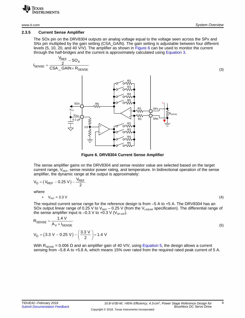
3.2.2.5 Load TestThe load test is done with test setup as shown in Figure 11. Table 5 lists the load test results. Figure 22shows the test results with trapezoidal control at 2.28-ARMS winding current and 100% duty cycle, andFigure 23 shows the results thermal image of the board after 10 minutes of continuous running. Themaximum temperature observed on the MOSFET is 81.4°C. Figure 24 shows the test results withsinusoidal control at a 2.37-ARMS winding current, and Figure 25 shows the thermal image of the boardafter 10 minutes of continuous running. The maximum temperature observed on the MOSFET is 85.9°C.
Figure 24 shows the test results with sinusoidal control at 2.5-A winding current.
Table 5. Load Test Results at 10.8-V DC
CONTROLMETHOD VDC (V) IDC (A)
WINDINGCURRENT (RMS)
(A)INPUT POWER (W)
MAXIMUM ICTEMPERATURE
(°C)Trapezoidal control 10.8 2.70 2.28 29.16 81.4Sinusoidal control 10.8 2.72 2.37 29.4 85.9
Figure 22. Load Test Results With Trapezoidal Control at 2.28-ARMS Winding Current, 100% Duty Cycle
Figure 23. Thermal Image of Board With Trapezoidal Control at 2.28-ARMS Winding Current,100% Duty Cycle
Motor winding current
Motor phase voltage to board GND
Hardware, Software, Testing Requirements, and Test Results www.ti.com
22 TIDUE42–February 2018Submit Documentation Feedback
Copyright © 2018, Texas Instruments Incorporated
10.8-V/30-W, >95% Efficiency, 4.3-cm2, Power Stage Reference Design forBrushless DC Servo Drive
Figure 24. Load Test Results With Sinusoidal Control at 2.37-ARMS Winding Current
Figure 25. Thermal Image of Board With Sinusoidal Control at 2.37-ARMS Winding Current

Board Output Power (W)
Effi
cien
cy (
)
5 10 15 20 25 30 3590
91
92
93
94
95
96
97
98
99
100
D001
95 Duty Cycle, 20kHz PWM Frequency100 Duty Cycle
www.ti.com Hardware, Software, Testing Requirements, and Test Results
23TIDUE42–February 2018Submit Documentation Feedback
Copyright © 2018, Texas Instruments Incorporated
10.8-V/30-W, >95% Efficiency, 4.3-cm2, Power Stage Reference Design forBrushless DC Servo Drive
3.2.2.6 Power Stage Efficiency TestThe reference design board power stage efficiency is experimentally tested with a test setup as shown inFigure 11. Table 6 lists the test results without heat sink at a 100% duty cycle. Table 7 lists the test resultswithout heat sink at a 95% duty cycle.
Table 6. Inverter Efficiency Test Results at 100% Duty Cycle Without Heat Sink and Without Airflow
INPUT DCVOLTAGE (V)
INPUT DCCURRENT (A)
INPUT DC POWER(W)
MOTOR WINDINGRMS CURRENT (A)
BOARD OUTPUTPOWER (W) EFFICIENCY (%)
10.63 0.859 9.13 0.792 8.93 97.7310.81 1.031 11.15 0.932 10.89 97.6610.78 1.207 13.02 1.074 12.70 97.5610.75 1.411 15.17 1.239 14.78 97.4410.91 1.678 18.31 1.460 17.79 97.1310.87 1.965 21.35 1.698 20.65 96.7310.80 2.378 25.67 2.039 24.70 96.2110.73 2.785 29.87 2.362 28.62 95.8010.69 2.989 31.95 2.507 30.51 95.51
Table 7. Inverter Efficiency Test Results at 95% Duty Cycle Without Heat Sink and Without Airflow
INPUT DCVOLTAGE (V)
INPUT DCCURRENT (A)
INPUT DC POWER(W)
MOTOR WINDINGRMS CURRENT (A)
BOARD OUTPUTPOWER (W) EFFICIENCY (%)
10.91 0.667 7.27 0.661 7.02 96.4710.87 0.886 9.63 0.845 9.28 96.4110.83 1.156 12.52 1.070 12.03 96.1310.78 1.448 15.61 1.325 14.96 95.8510.90 1.813 19.76 1.634 18.85 95.3610.81 2.191 23.69 1.959 22.48 94.8810.77 2.490 26.81 2.215 25.35 94.5310.69 3.002 32.10 2.657 30.21 94.12
Figure 26 shows the efficiency curve of these test conditions.
Figure 26. Power Stage Efficiency versus Output Power
The low RDS(on) of the CSD87502Q2 MOSFET power blocks along with clean MOSFET switching by theDRV8304 smart gate driver enable maximum three-phase inverter efficiency. The thermal pads on theMOSFET power blocks help to extract the heat to the PCB.

Winding current
Motor phase voltage to board GND
FAULT
PWM from MCU
Hardware, Software, Testing Requirements, and Test Results www.ti.com
24 TIDUE42–February 2018Submit Documentation Feedback
Copyright © 2018, Texas Instruments Incorporated
10.8-V/30-W, >95% Efficiency, 4.3-cm2, Power Stage Reference Design forBrushless DC Servo Drive
3.2.2.7 Overcurrent Limit ResultsThe gate driver DRV8304 implement adjustable VDS monitors to detect overcurrent or short conditions onthe external MOSFETs. The high-side VDS monitors measure the voltage between the VDRAIN and SHXpins. In configuration with three current shunt amplifiers, the low-side VDS monitors measure the voltagebetween the SHX and SPX pins.
When the voltage monitored is greater than the VDS trip point (VDS,OCP) after the VDS deglitch time (tDS,OCP)has expired, the DRV8304 detects an OCP condition and takes action according to the fault setting. In thehardware version of the DRV8304, the VDS monitor acts in automatic retry mode with a 4-ms retry time.
Figure 27 shows the VDS overcurrent action with the VDS reference voltage set to 0.15 V.
Assuming the junction temperature of 75°C, the RDS(on) at 75°C ≈ 34 mΩ (approximately 1.26 times theRDS(on) at 25°C, from the CSD87502Q2 data sheet).
where:• VDS deglitch time (tDS,OCP) = 4.5 μs• Current limit threshold = VDS threshold / RDS(on) = 4.41 A
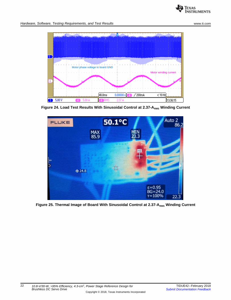
Figure 27 shows that the current is limited at 4.6 A. Figure 28 shows the zoomed view where the PWMshuts off when the current hits the over current threshold and the fault is created. The fault resets after 4ms.
Figure 27. Overcurrent Protection With MOSFET VDS Monitoring
Winding current
Motor phase voltage to board GND
FAULT
PWM from MCU
www.ti.com Hardware, Software, Testing Requirements, and Test Results
25TIDUE42–February 2018Submit Documentation Feedback
Copyright © 2018, Texas Instruments Incorporated
10.8-V/30-W, >95% Efficiency, 4.3-cm2, Power Stage Reference Design forBrushless DC Servo Drive
Figure 28. Zoomed View of Overcurrent Protection With MOSFET VDS Monitoring
3.2.2.8 BLDC Motor 60° Electrical Position Control With Trapezoidal ExcitationPosition control algorithm on the MSP430FR5949 is implemented using port interrupts capability of theMSP430 MCU. The testing is done on the BLDC motor that has three digital Hall position sensors.
Figure 29 and Figure 30 show the position control test results with a BLDC motor having four pole pairsand no gear assembly. Figure 29 shows the position control at 105° mechanical (420° electrical) with aholding torque equivalent to 2 A.
Figure 30 shows the test result with step change in mechanical position reference from 37.5° mechanicalto 82.5° mechanical with a 1.5-A holding current.

Winding current
Three Hall sensor multiplexed signal
Single Hall sensor output
Holding
current = 1.5 A
Position = 37.5° Mechanical(4-pole pair motor)
Position = 82.5° Mechanical(4-pole pair motor)
Winding Current
Three Hall sensor multiplexed signal
Single Hall sensor output
Holding current = 2 A
Motor position overshoot
Position = 105° Mechanical(4-pole pair motor)
Hardware, Software, Testing Requirements, and Test Results www.ti.com
26 TIDUE42–February 2018Submit Documentation Feedback
Copyright © 2018, Texas Instruments Incorporated
10.8-V/30-W, >95% Efficiency, 4.3-cm2, Power Stage Reference Design forBrushless DC Servo Drive
Figure 29. Test Results for Position Control at 105° Mechanical
Figure 30. Test Results for Position Control With a Step Change in Position Reference

www.ti.com Design Files
27TIDUE42–February 2018Submit Documentation Feedback
Copyright © 2018, Texas Instruments Incorporated
10.8-V/30-W, >95% Efficiency, 4.3-cm2, Power Stage Reference Design forBrushless DC Servo Drive
4 Design Files
4.1 SchematicsTo download the schematics, see the design files at TIDA-01587.
4.2 Bill of MaterialsTo download the bill of materials (BOM), see the design files at TIDA-01587.
4.3 PCB Layout Recommendations
4.3.1 Layout PrintsTo download the layer plots, see the design files at TIDA-01587.
4.4 Altium ProjectTo download the Altium project files, see the design files at TIDA-01587.
4.5 Gerber FilesTo download the Gerber files, see the design files at TIDA-01587.
4.6 Assembly DrawingsTo download the assembly drawings, see the design files at TIDA-01587.
5 Software FilesTo download the software files, see the design files at TIDA-01587.
6 Related Documentation1. Texas Instruments, Field Oriented Control (FOC) Made Easy for Brushless DC (BLDC) Motors Using
TI Smart Gate Drivers Application Brief2. Texas Instruments, DRV8304 38-V 3-Phase Smart Gate Driver Data Sheet
6.1 TrademarksE2E, MSP430, Code Composer Studio are trademarks of Texas Instruments.All other trademarks are the property of their respective owners.
7 TerminologyBLDC— Brushless DC
ESD— Electrostatic discharge
MCU— Microcontroller unit
PWM— Pulse width modulation

About the Authors www.ti.com
28 TIDUE42–February 2018Submit Documentation Feedback
Copyright © 2018, Texas Instruments Incorporated
10.8-V/30-W, >95% Efficiency, 4.3-cm2, Power Stage Reference Design forBrushless DC Servo Drive
8 About the AuthorsMANU BALAKRISHNAN is a systems engineer at Texas Instruments, where he is responsible fordeveloping subsystem design solutions for the Industrial Motor Drive systems. Manu brings to this role hisexperience in power electronics and analog and mixed signal designs. He has system level productdesign experience in permanent magnet motor drives. Manu earned his bachelor of technology inelectrical and electronics engineering from the University of Kerala and his master of technology in powerelectronics from National Institute of Technology Calicut, India.
VARAD JOSHI is a project trainee in the Industrial Systems team at Texas Instruments, where he islearning and developing reference design solutions with a focus on motor drive systems. Varad is a final-year student pursuing a bachelor of engineering (B.E. hons) in electrical and electronics engineering fromBirla Institute of Technology & Sciences (BITS), Pilani, Goa.
JASRAJ DALVI is an end equipment lead with Industrial Systems team at Texas Instruments, where he isresponsible for defining reference design solutions and control algorithms for motor control systems. Hecompleted his bachelors of engineering degree in electrical engineering from University of Pune, India andhis post-graduate diploma in marketing management at S.I.B.M. in Pune, India.

IMPORTANT NOTICE FOR TI DESIGN INFORMATION AND RESOURCES
Texas Instruments Incorporated (‘TI”) technical, application or other design advice, services or information, including, but not limited to,reference designs and materials relating to evaluation modules, (collectively, “TI Resources”) are intended to assist designers who aredeveloping applications that incorporate TI products; by downloading, accessing or using any particular TI Resource in any way, you(individually or, if you are acting on behalf of a company, your company) agree to use it solely for this purpose and subject to the terms ofthis Notice.TI’s provision of TI Resources does not expand or otherwise alter TI’s applicable published warranties or warranty disclaimers for TIproducts, and no additional obligations or liabilities arise from TI providing such TI Resources. TI reserves the right to make corrections,enhancements, improvements and other changes to its TI Resources.You understand and agree that you remain responsible for using your independent analysis, evaluation and judgment in designing yourapplications and that you have full and exclusive responsibility to assure the safety of your applications and compliance of your applications(and of all TI products used in or for your applications) with all applicable regulations, laws and other applicable requirements. Yourepresent that, with respect to your applications, you have all the necessary expertise to create and implement safeguards that (1)anticipate dangerous consequences of failures, (2) monitor failures and their consequences, and (3) lessen the likelihood of failures thatmight cause harm and take appropriate actions. You agree that prior to using or distributing any applications that include TI products, youwill thoroughly test such applications and the functionality of such TI products as used in such applications. TI has not conducted anytesting other than that specifically described in the published documentation for a particular TI Resource.You are authorized to use, copy and modify any individual TI Resource only in connection with the development of applications that includethe TI product(s) identified in such TI Resource. NO OTHER LICENSE, EXPRESS OR IMPLIED, BY ESTOPPEL OR OTHERWISE TOANY OTHER TI INTELLECTUAL PROPERTY RIGHT, AND NO LICENSE TO ANY TECHNOLOGY OR INTELLECTUAL PROPERTYRIGHT OF TI OR ANY THIRD PARTY IS GRANTED HEREIN, including but not limited to any patent right, copyright, mask work right, orother intellectual property right relating to any combination, machine, or process in which TI products or services are used. Informationregarding or referencing third-party products or services does not constitute a license to use such products or services, or a warranty orendorsement thereof. Use of TI Resources may require a license from a third party under the patents or other intellectual property of thethird party, or a license from TI under the patents or other intellectual property of TI.TI RESOURCES ARE PROVIDED “AS IS” AND WITH ALL FAULTS. TI DISCLAIMS ALL OTHER WARRANTIES ORREPRESENTATIONS, EXPRESS OR IMPLIED, REGARDING TI RESOURCES OR USE THEREOF, INCLUDING BUT NOT LIMITED TOACCURACY OR COMPLETENESS, TITLE, ANY EPIDEMIC FAILURE WARRANTY AND ANY IMPLIED WARRANTIES OFMERCHANTABILITY, FITNESS FOR A PARTICULAR PURPOSE, AND NON-INFRINGEMENT OF ANY THIRD PARTY INTELLECTUALPROPERTY RIGHTS.TI SHALL NOT BE LIABLE FOR AND SHALL NOT DEFEND OR INDEMNIFY YOU AGAINST ANY CLAIM, INCLUDING BUT NOTLIMITED TO ANY INFRINGEMENT CLAIM THAT RELATES TO OR IS BASED ON ANY COMBINATION OF PRODUCTS EVEN IFDESCRIBED IN TI RESOURCES OR OTHERWISE. IN NO EVENT SHALL TI BE LIABLE FOR ANY ACTUAL, DIRECT, SPECIAL,COLLATERAL, INDIRECT, PUNITIVE, INCIDENTAL, CONSEQUENTIAL OR EXEMPLARY DAMAGES IN CONNECTION WITH ORARISING OUT OF TI RESOURCES OR USE THEREOF, AND REGARDLESS OF WHETHER TI HAS BEEN ADVISED OF THEPOSSIBILITY OF SUCH DAMAGES.You agree to fully indemnify TI and its representatives against any damages, costs, losses, and/or liabilities arising out of your non-compliance with the terms and provisions of this Notice.This Notice applies to TI Resources. Additional terms apply to the use and purchase of certain types of materials, TI products and services.These include; without limitation, TI’s standard terms for semiconductor products http://www.ti.com/sc/docs/stdterms.htm), evaluationmodules, and samples (http://www.ti.com/sc/docs/sampterms.htm).
Mailing Address: Texas Instruments, Post Office Box 655303, Dallas, Texas 75265Copyright © 2018, Texas Instruments Incorporated


