© 2009 Pearson Education, Upper Saddle River, NJ 07458. All Rights ReservedFloyd, Digital Fundamentals, 10th ed
Digital Fundamentals
Tenth Edition
Floyd
Chapter 7
© 2008 Pearson Education
© 2009 Pearson Education, Upper Saddle River, NJ 07458. All Rights ReservedFloyd, Digital Fundamentals, 10th ed
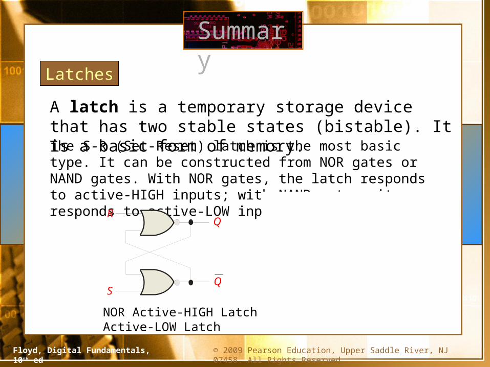
A latch is a temporary storage device that has two stable states (bistable). It is a basic form of memory.
Summary
Latches
The S-R (Set-Reset) latch is the most basic type. It can be constructed from NOR gates or NAND gates. With NOR gates, the latch responds to active-HIGH inputs; with NAND gates, it responds to active-LOW inputs.
NOR Active-HIGH Latch NAND Active-LOW Latch
R
S
Q Q
Q
S
RQ

© 2009 Pearson Education, Upper Saddle River, NJ 07458. All Rights ReservedFloyd, Digital Fundamentals, 10th ed
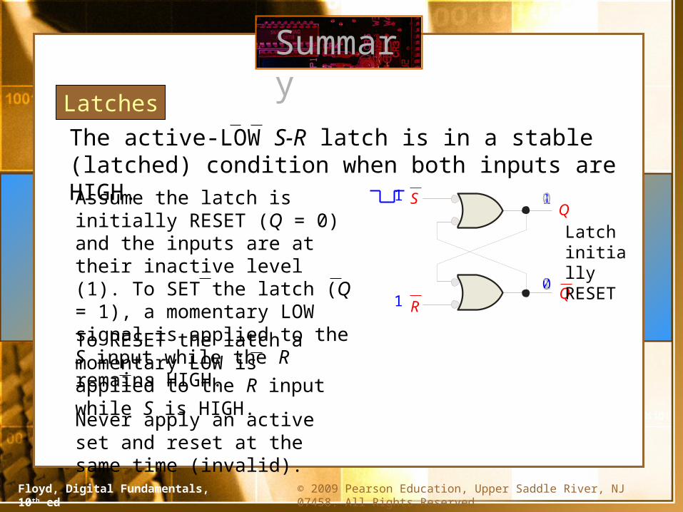
The active-HIGH S-R latch is in a stable (latched) condition when both inputs are LOW.
Summary
Latches
R
S
Q
Q
Assume the latch is initially RESET (Q = 0) and the inputs are at their inactive level (0). To SET the latch (Q = 1), a momentary HIGH signal is applied to the S input while the R remains LOW.
0 1
0
R
S
Q
Q
1
0
0
To RESET the latch (Q = 0), a momentary HIGH signal is applied to the R input while the S remains LOW.
0
0
1
01
0
Latch initially RESET
Latch initially SET
© 2009 Pearson Education, Upper Saddle River, NJ 07458. All Rights ReservedFloyd, Digital Fundamentals, 10th ed
S
R
The active-LOW S-R latch is in a stable (latched) condition when both inputs are HIGH.
Summary
Latches
Q
Q
1 1
01
0
1
Latch initially RESET
Q
Q
1
1
01
01
Latch initially SET
S
R
Assume the latch is initially RESET (Q = 0) and the inputs are at their inactive level (1). To SET the latch (Q = 1), a momentary LOW signal is applied to the S input while the R remains HIGH.
To RESET the latch a momentary LOW is applied to the R input while S is HIGH.
Never apply an active set and reset at the same time (invalid).

© 2009 Pearson Education, Upper Saddle River, NJ 07458. All Rights ReservedFloyd, Digital Fundamentals, 10th ed
The active-LOW S-R latch is available as the 74LS279A IC.
Summary
Latches
(5)
1S1(2)
(1)
(6)
1R
2S
2R
1S2(4)
(9)
(13)
(7)
(3)
(14)
3S1(11)
(10)
(15)
3R
4S
4R
3S2(12)
1Q
2Q
3Q
4Q
74LS279A
It features four internal latches with two having two S inputs. To SET any of the latches, the S line is pulsed low. It is available in several packages.
1
2
Position 1 to 2
Position 2 to 1
S
R
Q
VCC
S-R latches are frequently used for switch debounce circuits as shown:
S
R
© 2009 Pearson Education, Upper Saddle River, NJ 07458. All Rights ReservedFloyd, Digital Fundamentals, 10th ed
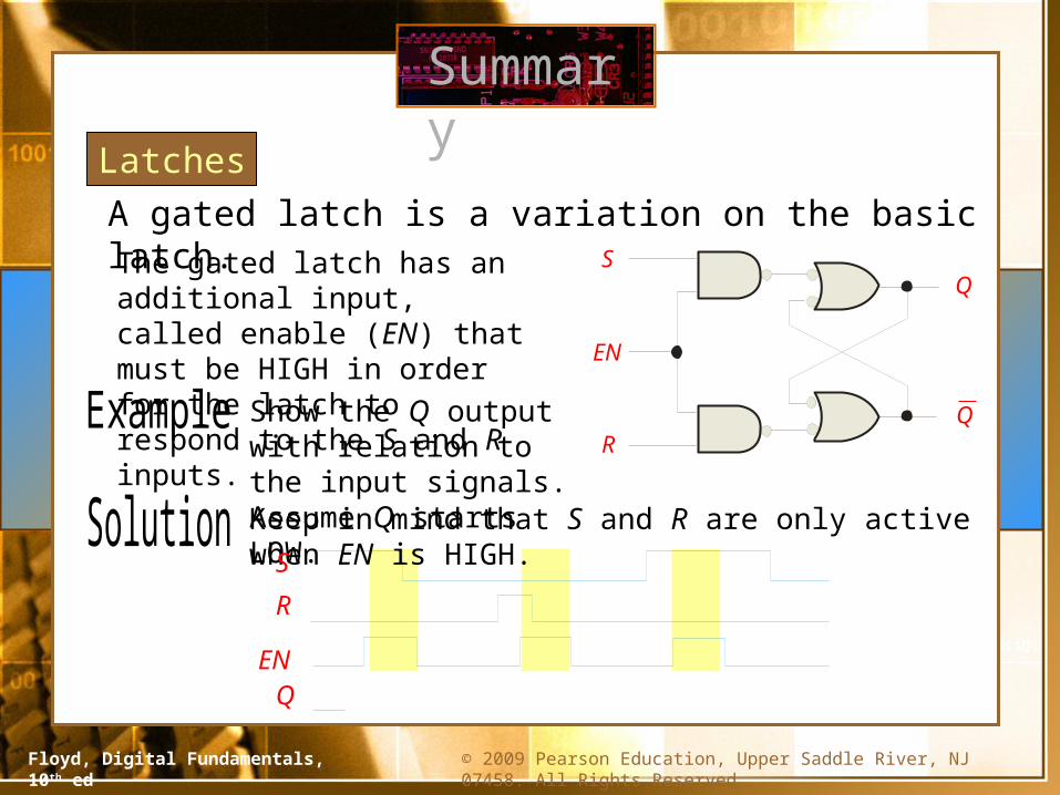
A gated latch is a variation on the basic latch.
Summary
Latches
The gated latch has an additional input, called enable (EN) that must be HIGH in order for the latch to respond to the S and R inputs.
R
SQ
Q
EN
Show the Q output with relation to the input signals. Assume Q starts LOW.Keep in mind that S and R are only active when EN is HIGH.
S
R
ENQ
© 2009 Pearson Education, Upper Saddle River, NJ 07458. All Rights ReservedFloyd, Digital Fundamentals, 10th ed
Summary
Latches
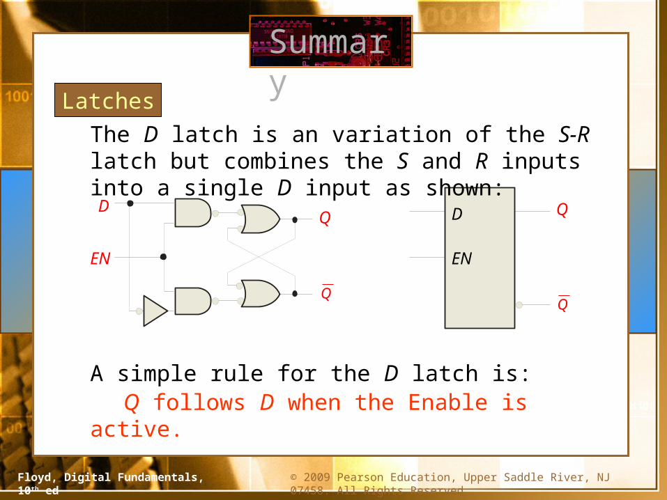
The D latch is an variation of the S-R latch but combines the S and R inputs into a single D input as shown:
A simple rule for the D latch is: Q follows D when the Enable is active.
D
EN
Q
QD
EN
© 2009 Pearson Education, Upper Saddle River, NJ 07458. All Rights ReservedFloyd, Digital Fundamentals, 10th ed
Summary
Latches
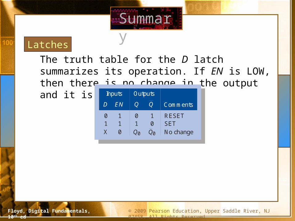
The truth table for the D latch summarizes its operation. If EN is LOW, then there is no change in the output and it is latched.
Inputs
Comments
01X
END
110
Outputs
01Q0
10Q0
RESETSETNo change
© 2009 Pearson Education, Upper Saddle River, NJ 07458. All Rights ReservedFloyd, Digital Fundamentals, 10th ed
Summary
Latches
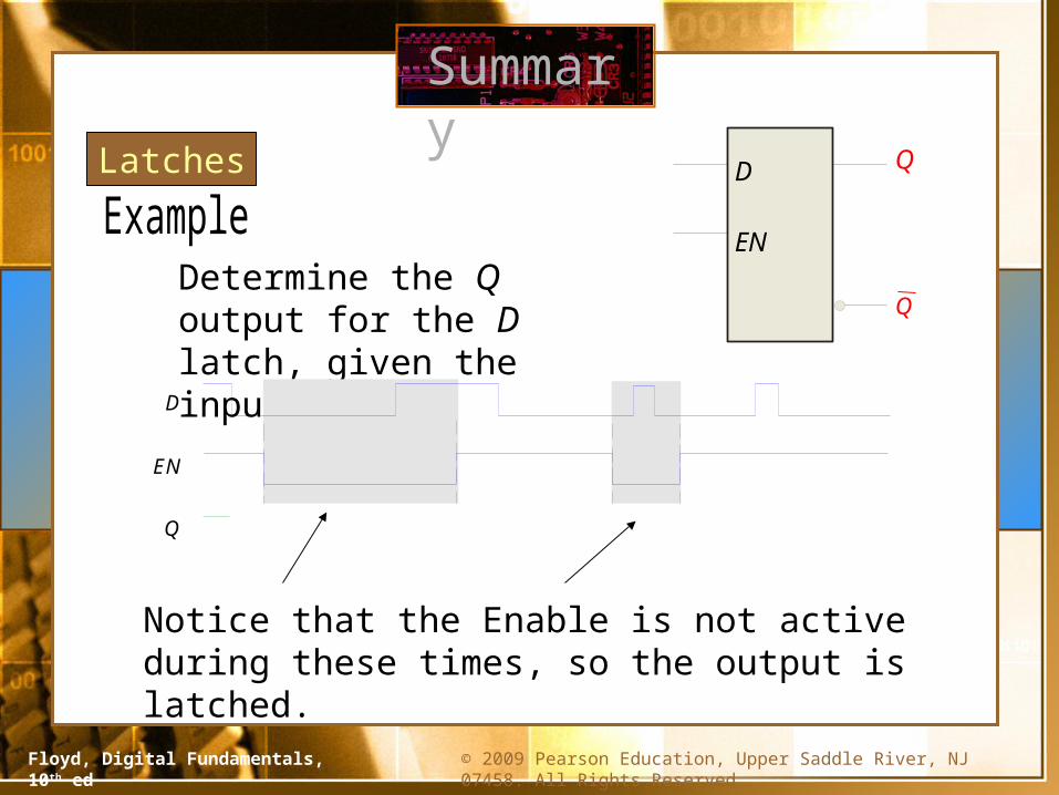
Determine the Q output for the D latch, given the inputs shown.
EN
Q
D
Notice that the Enable is not active during these times, so the output is latched.
Q
QD
EN

© 2009 Pearson Education, Upper Saddle River, NJ 07458. All Rights ReservedFloyd, Digital Fundamentals, 10th ed
Summary
Flip-flops
A flip-flop differs from a latch in the manner it changes states. A flip-flop is a clocked device, in which only the clock edge determines when a new bit is entered.
The active edge can be positive or negative.
D Q
C
Q
(a) Positive edge-triggered
D Q
C
Q
(b) Negative edge-triggered
Dynamic input indicator

© 2009 Pearson Education, Upper Saddle River, NJ 07458. All Rights ReservedFloyd, Digital Fundamentals, 10th ed
Summary
Flip-flops
The truth table for a positive-edge triggered D flip-flop shows an up arrow to remind you that it is sensitive to its D input only on the rising edge of the clock; otherwise it is latched. The truth table for a negative-edge triggered D flip-flop is identical except for the direction of the arrow.
Inputs
Comments
1
CLKD
Outputs
1
0 SET0 0 1 RESET
Inputs
Comments
1
CLKD
Outputs
1
0 SET0 0 1 RESET
(a) Positive-edge triggered (b) Negative-edge triggered

© 2009 Pearson Education, Upper Saddle River, NJ 07458. All Rights ReservedFloyd, Digital Fundamentals, 10th ed
Summary
Flip-flops
The J-K flip-flop is more versatile than the D flip flop. In addition to the clock input, it has two inputs, labeled J and K. When both J and K = 1, the output changes states (toggles) on the active clock edge (in this case, the rising edge).
Inputs
Comments
1
1 1
1
CLKKJ
Outputs
1
Q0
Q0
Q0
Q0
0 SETToggle
0
0
00 0 1 RESET
No change
© 2009 Pearson Education, Upper Saddle River, NJ 07458. All Rights ReservedFloyd, Digital Fundamentals, 10th ed
Summary
Flip-flops
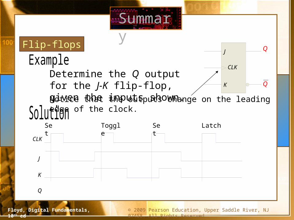
Determine the Q output for the J-K flip-flop, given the inputs shown.
CLK
Q
K
J
CLK
K
J
Q
Q
Notice that the outputs change on the leading edge of the clock.
Set Toggle Set Latch

© 2009 Pearson Education, Upper Saddle River, NJ 07458. All Rights ReservedFloyd, Digital Fundamentals, 10th ed
Summary
Flip-flops
CLK
D
CLK
Q
Q
A D-flip-flop does not have a toggle mode like the J-K flip-flop, but you can hardwire a toggle mode by connecting Q back to D as shown. This is useful in some counters as you will see in Chapter 8.
For example, if Q is LOW, Q is HIGH and the flip-flop will toggle on the next clock edge. Because the flip-flop only changes on the active edge, the output will only change once for each clock pulse.
D flip-flop hardwired for a toggle mode
© 2009 Pearson Education, Upper Saddle River, NJ 07458. All Rights ReservedFloyd, Digital Fundamentals, 10th ed
Summary
Flip-flops
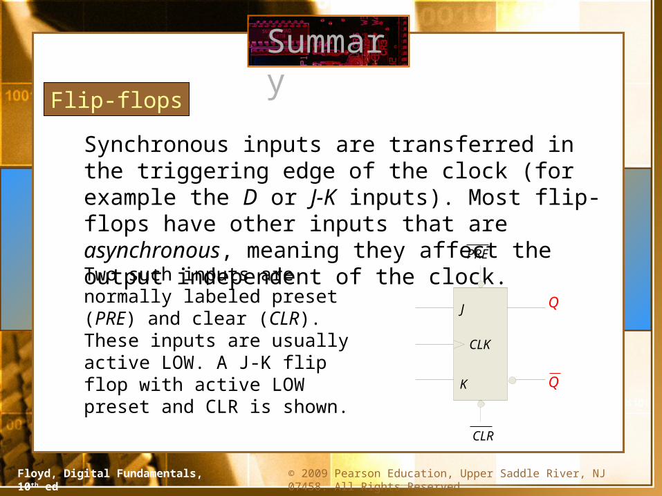
Synchronous inputs are transferred in the triggering edge of the clock (for example the D or J-K inputs). Most flip-flops have other inputs that are asynchronous, meaning they affect the output independent of the clock.
Two such inputs are normally labeled preset (PRE) and clear (CLR). These inputs are usually active LOW. A J-K flip flop with active LOW preset and CLR is shown.
CLK
K
J
Q
Q
PRE
CLR

© 2009 Pearson Education, Upper Saddle River, NJ 07458. All Rights ReservedFloyd, Digital Fundamentals, 10th ed
Summary
Flip-flopsFlip-flops
Determine the Q output for the J-K flip-flop, given the inputs shown.
CLK
K
J
Q
Q
PRE
CLR
Set Toggle Reset Toggle
Set
Set
Reset
Latch
CLK
K
J
Q
PRE
CLR
© 2009 Pearson Education, Upper Saddle River, NJ 07458. All Rights ReservedFloyd, Digital Fundamentals, 10th ed
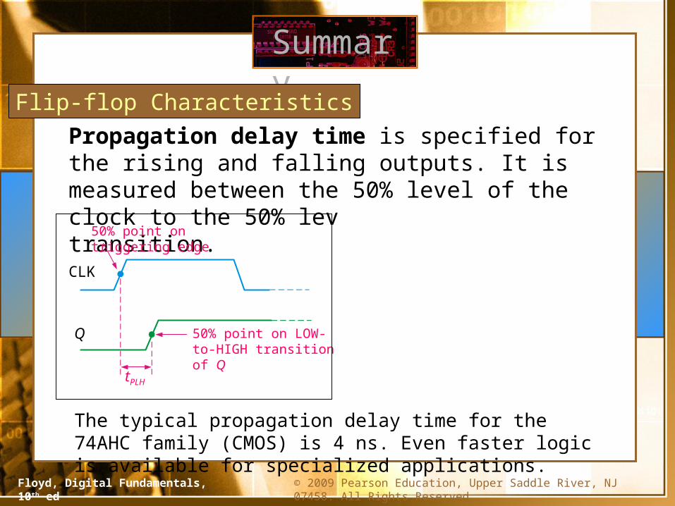
Propagation delay time is specified for the rising and falling outputs. It is measured between the 50% level of the clock to the 50% level of the output transition.
Summary
Flip-flop Characteristics
50% point on triggering edge
50% point
50% point on LOW-to-HIGH transition of Q
tPLH tPHL
CLK CLK
Q Q 50% point on HIGH-to- LOW transition of Q
The typical propagation delay time for the 74AHC family (CMOS) is 4 ns. Even faster logic is available for specialized applications.
© 2009 Pearson Education, Upper Saddle River, NJ 07458. All Rights ReservedFloyd, Digital Fundamentals, 10th ed
Another propagation delay time specification is the time required for an asynchronous input to cause a change in the output. Again it is measured from the 50% levels. The 74AHC family has specified delay times under 5 ns.
Summary
Flip-flop Characteristics
50% point
tPLHtPHL
Q 50% point50% point
50% point
Q
PRE CLR
© 2009 Pearson Education, Upper Saddle River, NJ 07458. All Rights ReservedFloyd, Digital Fundamentals, 10th ed
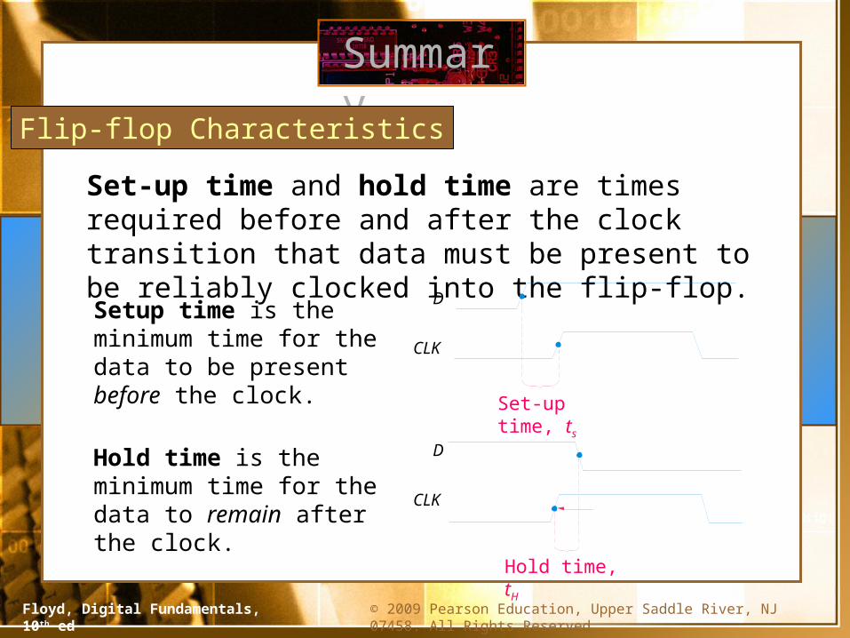
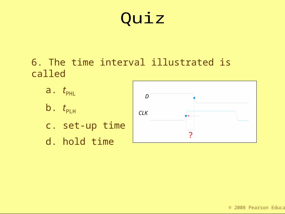
Set-up time and hold time are times required before and after the clock transition that data must be present to be reliably clocked into the flip-flop.
Summary
Flip-flop Characteristics
Setup time is the minimum time for the data to be present before the clock.
Hold time is the minimum time for the data to remain after the clock.
CLK
D
CLK
D
Set-up time, ts
Hold time, tH
© 2009 Pearson Education, Upper Saddle River, NJ 07458. All Rights ReservedFloyd, Digital Fundamentals, 10th ed
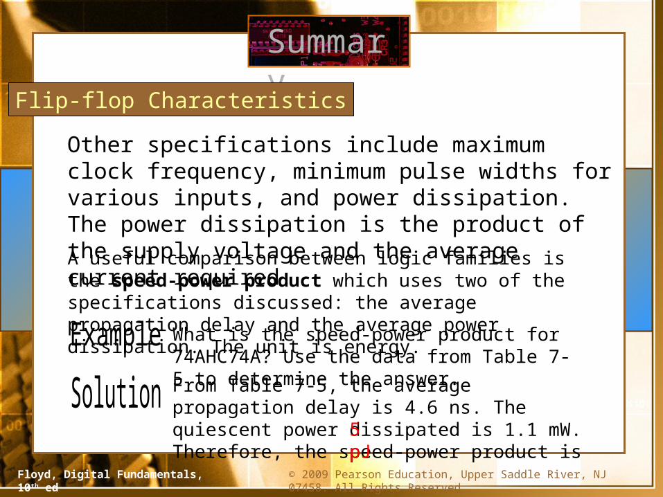
Other specifications include maximum clock frequency, minimum pulse widths for various inputs, and power dissipation. The power dissipation is the product of the supply voltage and the average current required.
Summary
Flip-flop Characteristics
A useful comparison between logic families is the speed-power product which uses two of the specifications discussed: the average propagation delay and the average power dissipation. The unit is energy.
What is the speed-power product for 74AHC74A? Use the data from Table 7-5 to determine the answer.
From Table 7-5, the average propagation delay is 4.6 ns. The quiescent power dissipated is 1.1 mW. Therefore, the speed-power product is 5 pJ

© 2009 Pearson Education, Upper Saddle River, NJ 07458. All Rights ReservedFloyd, Digital Fundamentals, 10th ed
Summary
Flip-flop Applications
Principal flip-flop applications are for temporary data storage, as frequency dividers, and in counters (which are covered in detail in Chapter 8).
Typically, for data storage applications, a group of flip-flops are connected to parallel data lines and clocked together. Data is stored until the next clock pulse.
D
C
R
D
C
R
D
C
R
D
C
R
Parallel data input lines
Clock
Clear
Output lines
Q0
Q1
Q2
Q3

© 2009 Pearson Education, Upper Saddle River, NJ 07458. All Rights ReservedFloyd, Digital Fundamentals, 10th ed
Summary
Flip-flop Applications
For frequency division, it is simple to use a flip-flop in the toggle mode or to chain a series of toggle flip flops to continue to divide by two.
One flip-flop will divide fin by 2, two flip-flops will divide fin by 4 (and so on). A side benefit of frequency division is that the output has an exact 50% duty cycle.
HIGH HIGH
CLK
K
JQA
CLK
K
J
fin
QB fout
Waveforms:
fin
fout
© 2009 Pearson Education, Upper Saddle River, NJ 07458. All Rights ReservedFloyd, Digital Fundamentals, 10th ed
Summary
One-Shots
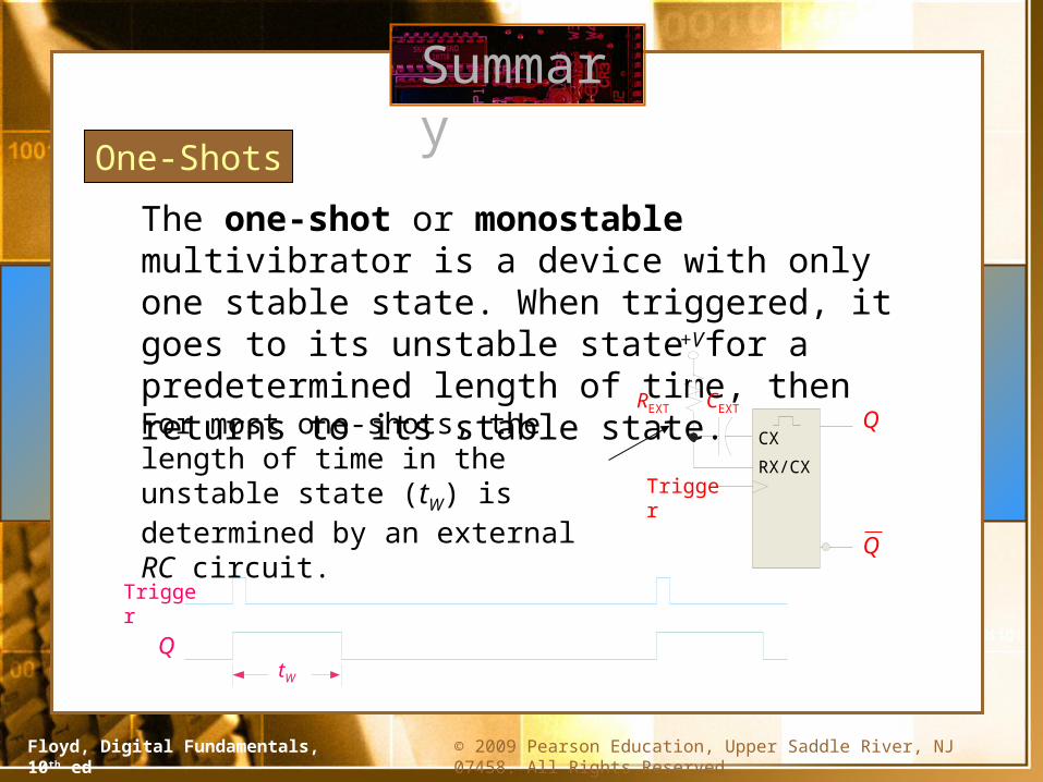
The one-shot or monostable multivibrator is a device with only one stable state. When triggered, it goes to its unstable state for a predetermined length of time, then returns to its stable state.
For most one-shots, the length of time in the unstable state (tW) is determined by an external RC circuit. Trigger
CEXTREXT
+V
CX
RX/CX
Q
Q
tW
Trigger
Q

© 2009 Pearson Education, Upper Saddle River, NJ 07458. All Rights ReservedFloyd, Digital Fundamentals, 10th ed
Summary
One-Shots
Retriggerable one-shots respond to any trigger, even if it occurs in the unstable state. If it occurs during the unstable state, the state is extended by an amount equal to the pulse width.
Retriggers
tW
Trigger
Q
Retriggerable one-shot:
Nonretriggerable one-shots do not respond to any triggers that occur during the unstable state.

© 2009 Pearson Education, Upper Saddle River, NJ 07458. All Rights ReservedFloyd, Digital Fundamentals, 10th ed
Summary
One-Shots
An application for a retriggerable one-shot is a power failure detection circuit. Triggers are derived from the ac power source, and continue to retrigger the one shot. In the event of a power failure, the one-shot is not triggered and an alarm can be initiated.
tW
tW
tW
Retriggers Retriggers
Triggers derived from ac
Q
Missing trigger due to power failure
Power failure indication

© 2009 Pearson Education, Upper Saddle River, NJ 07458. All Rights ReservedFloyd, Digital Fundamentals, 10th ed
(7)
(6)
(2)
(3)
(5)
(4) (8)
(1)
Summary
The 555 timer
The 555 timer can be configured in various ways, including as a one-shot. A basic one shot is shown. The pulse width is determined by R1C1 and is approximately tW = 1.1R1C1.
The trigger is a negative-going pulse.
RESETDISCH
THRES
TRIGGND
CONT
OUT
VCC
+VCC
tW = 1.1R1C1
C1
R1

© 2009 Pearson Education, Upper Saddle River, NJ 07458. All Rights ReservedFloyd, Digital Fundamentals, 10th ed
(7)
(6)
(2)
(3)
(5)
(4) (8)
(1)
Summary
The 555 timer
RESETDISCH
THRES
TRIGGND
CONT
OUT
VCC
+VCC
tW = 1.1R1C1
C1
R1
Determine the pulse width for the circuit shown. tW = 1.1R1C1 = 1.1(10 kW)(2.2 mF) =
10 kW
2.2 mF
24.2 ms
+15 V
© 2009 Pearson Education, Upper Saddle River, NJ 07458. All Rights ReservedFloyd, Digital Fundamentals, 10th ed
Summary
The 555 timer
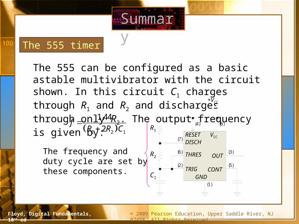
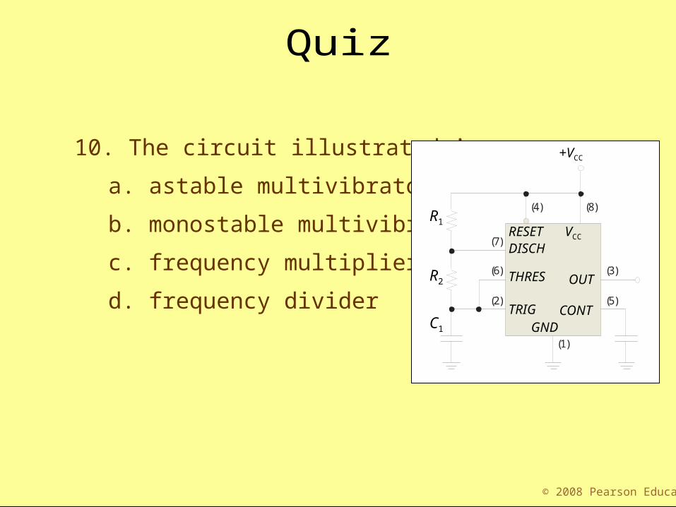
The 555 can be configured as a basic astable multivibrator with the circuit shown. In this circuit C1 charges through R1 and R2 and discharges through only R2. The output frequency is given by:
The frequency and duty cycle are set by these components.
1 2 1
1.44
2f
R R C
(7)
(6)
(2)
(3)
(5)
(4) (8)
(1)
RESETDISCH
THRES
TRIGGND
CONT
OUT
VCC
C1
R1
R2
+VCC
© 2009 Pearson Education, Upper Saddle River, NJ 07458. All Rights ReservedFloyd, Digital Fundamentals, 10th ed
Summary
The 555 timer
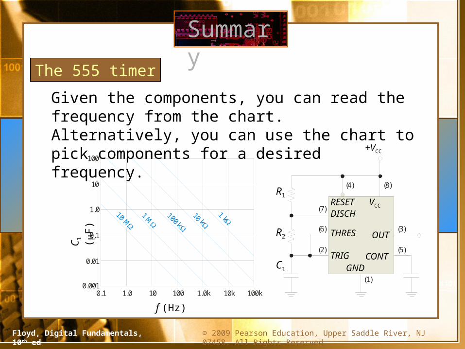
Given the components, you can read the frequency from the chart. Alternatively, you can use the chart to pick components for a desired frequency.
(7)
(6)
(2)
(3)
(5)
(4) (8)
(1)
RESETDISCH
THRES
TRIGGND
CONT
OUT
VCC
C1
R1
R2
+VCC
10
1.0
0.1
0.01
0.0010.1 1.0 10 100 1.0k 10k 100k
100
C1 (m
F)
f (Hz)
© 2009 Pearson Education, Upper Saddle River, NJ 07458. All Rights ReservedFloyd, Digital Fundamentals, 10th ed
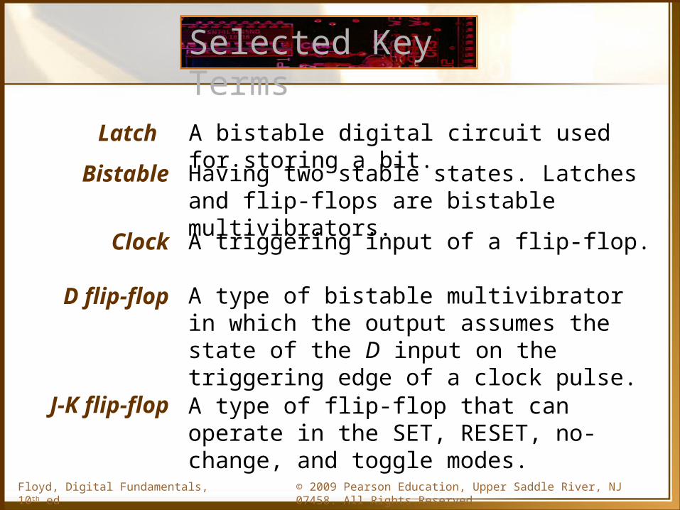
Selected Key Terms
Latch
Bistable
Clock
D flip-flop
J-K flip-flop
A bistable digital circuit used for storing a bit.
Having two stable states. Latches and flip-flops are bistable multivibrators.
A triggering input of a flip-flop.
A type of bistable multivibrator in which the output assumes the state of the D input on the triggering edge of a clock pulse.
A type of flip-flop that can operate in the SET, RESET, no-change, and toggle modes.
© 2009 Pearson Education, Upper Saddle River, NJ 07458. All Rights ReservedFloyd, Digital Fundamentals, 10th ed
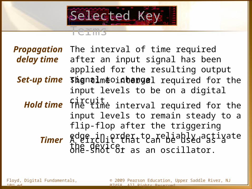
Selected Key Terms
Propagation delay time
Set-up time
Hold time
Timer
The interval of time required after an input signal has been applied for the resulting output signal to change.The time interval required for the input levels to be on a digital circuit.
The time interval required for the input levels to remain steady to a flip-flop after the triggering edge in order to reliably activate the device.
A circuit that can be used as a one-shot or as an oscillator.
© 2009 Pearson Education, Upper Saddle River, NJ 07458. All Rights ReservedFloyd, Digital Fundamentals, 10th ed
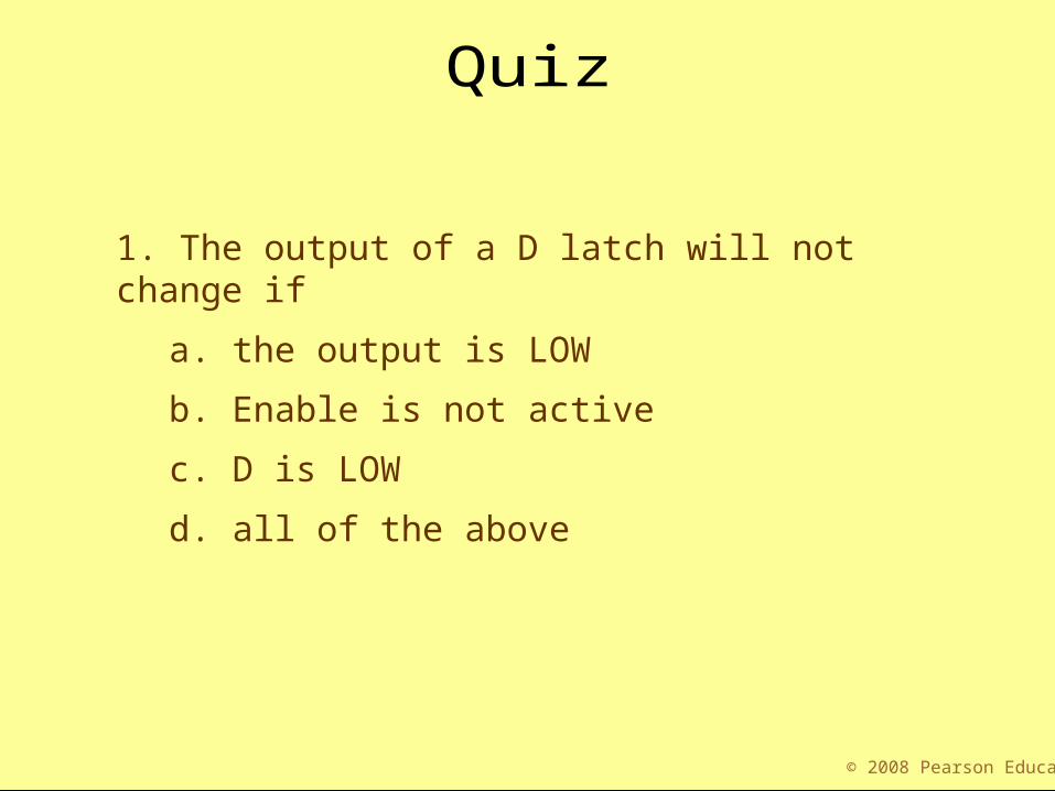
1. The output of a D latch will not change if
a. the output is LOW
b. Enable is not active
c. D is LOW
d. all of the above
© 2008 Pearson Education

© 2009 Pearson Education, Upper Saddle River, NJ 07458. All Rights ReservedFloyd, Digital Fundamentals, 10th ed
2. The D flip-flop shown will
a. set on the next clock pulse
b. reset on the next clock pulse
c. latch on the next clock pulse
d. toggle on the next clock pulse
© 2008 Pearson Education
CLK
D
CLK
Q
Q

© 2009 Pearson Education, Upper Saddle River, NJ 07458. All Rights ReservedFloyd, Digital Fundamentals, 10th ed
3. For the J-K flip-flop shown, the number of inputs that are asynchronous is
a. 1
b. 2
c. 3
d. 4
© 2008 Pearson Education
CLK
K
J
Q
Q
PRE
CLR
© 2009 Pearson Education, Upper Saddle River, NJ 07458. All Rights ReservedFloyd, Digital Fundamentals, 10th ed
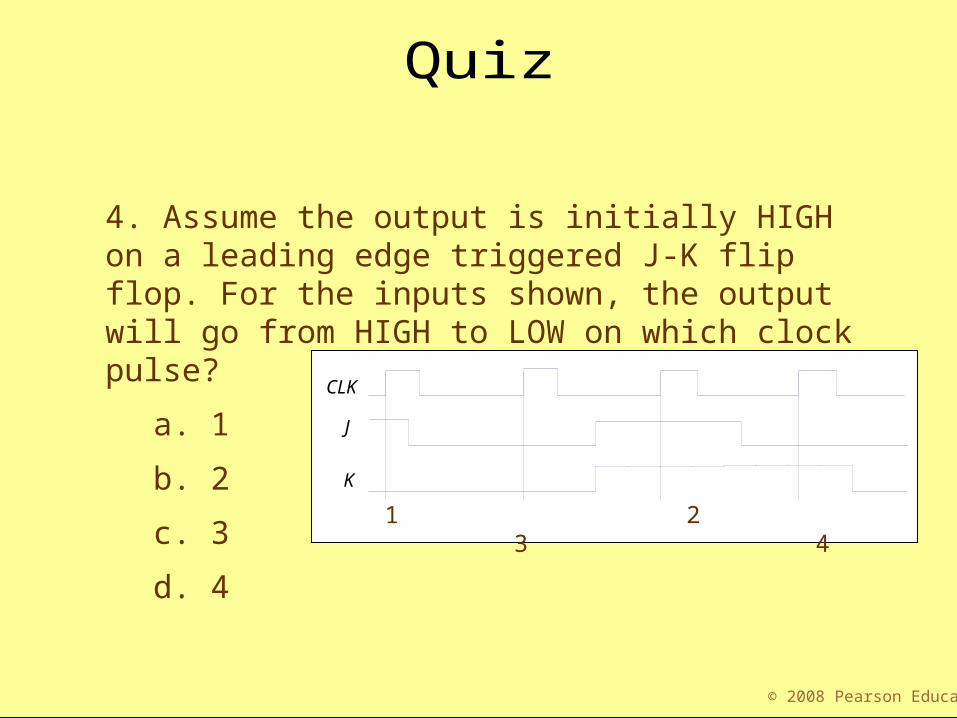
4. Assume the output is initially HIGH on a leading edge triggered J-K flip flop. For the inputs shown, the output will go from HIGH to LOW on which clock pulse?
a. 1
b. 2
c. 3
d. 4
© 2008 Pearson Education
CLK
K
J
1 2 3 4

© 2009 Pearson Education, Upper Saddle River, NJ 07458. All Rights ReservedFloyd, Digital Fundamentals, 10th ed
5. The time interval illustrated is called
a. tPHL
b. tPLH
c. set-up time
d. hold time
© 2008 Pearson Education
50% point on triggering edge
50% point on LOW-to-HIGH transition of Q
CLK
Q
?
© 2009 Pearson Education, Upper Saddle River, NJ 07458. All Rights ReservedFloyd, Digital Fundamentals, 10th ed© 2008 Pearson Education
CLK
D
?
6. The time interval illustrated is called
a. tPHL
b. tPLH
c. set-up time
d. hold time

© 2009 Pearson Education, Upper Saddle River, NJ 07458. All Rights ReservedFloyd, Digital Fundamentals, 10th ed
7. The application illustrated is a
a. astable multivibrator
b. data storage device
c. frequency multiplier
d. frequency divider
© 2008 Pearson Education
HIGH HIGH
CLK
K
JQA
CLK
K
J
fin
QBfout

© 2009 Pearson Education, Upper Saddle River, NJ 07458. All Rights ReservedFloyd, Digital Fundamentals, 10th ed© 2008 Pearson Education
8. The application illustrated is a
a. astable multivibrator
b. data storage device
c. frequency multiplier
d. frequency divider
D
C
R
D
C
R
D
C
R
D
C
R
Parallel data input lines
Clock
Clear
Output lines
Q0
Q1
Q2
Q3
© 2009 Pearson Education, Upper Saddle River, NJ 07458. All Rights ReservedFloyd, Digital Fundamentals, 10th ed
9. A retriggerable one-shot with an active HIGH output has a pulse width of 20 ms and is triggered from a 60 Hz line. The output will be a
a. series of 16.7 ms pulses
b. series of 20 ms pulses
c. constant LOW
d. constant HIGH
© 2008 Pearson Education
© 2009 Pearson Education, Upper Saddle River, NJ 07458. All Rights ReservedFloyd, Digital Fundamentals, 10th ed© 2008 Pearson Education
10. The circuit illustrated is a
a. astable multivibrator
b. monostable multivibrator
c. frequency multiplier
d. frequency divider
(7)
(6)
(2)
(3)
(5)
(4) (8)
(1)
RESETDISCH
THRES
TRIGGND
CONT
OUT
VCC
+VCC
C1
R1
R2

© 2009 Pearson Education, Upper Saddle River, NJ 07458. All Rights ReservedFloyd, Digital Fundamentals, 10th ed
Answers:
1. b
2. d
3. b
4. c
5. b
6. d
7. d
8. b
9. d
10. a


