dosignalcontrolunt - p. · is a block diagram for explaining a write leveling operation in the ddr3...
TRANSCRIPT
United States Patent
US008020022B2
(12) (10) Patent No.: US 8,020,022 B2 Tokuhiro (45) Date of Patent: Sep. 13, 2011
(54) DELAYTIME CONTROL OF MEMORY (56) References Cited CONTROLLER
U.S. PATENT DOCUMENTS
(75) Inventor: Noriyuki Tokuhiro, Kawasaki (JP) 7,412,616 B2 * 8/2008 Matsui et al. ................. T13/401 7,796.465 B2* 9/2010 Swain et al. ............. 365,233.13
(73) Assignee: Fujitsu Limited, Kawasaki (JP) 2005/00471.92 A1 3, 2005 Matsui et al. 2005/0174878 A1 8, 2005 Osaka et al.
(*) Notice: Subject to any disclaimer, the term of this FOREIGN PATENT DOCUMENTS patent is extended or adjusted under 35 JP 2003-099321 4/2003 U.S.C. 154(b) by 334 days. JP 2005-078547 3, 2005
JP 2005-209168 8, 2005
(21) Appl. No.: 12/209,740 * cited by examiner
(22) Filed: Sep. 12, 2008 Primary Examiner — Raymond Phan (74) Attorney, Agent, or Firm — Staas & Halsey LLP
(65) Prior Publication Data (57) ABSTRACT
US 2009/OO77411A1 Mar. 19, 2009 A memory control circuit has a write leveling function and O O controls read/write operations by Supplying a clock signal to
(30) Foreign Application Priority Data a plurality of memories through a clock signal line which is Sep. 18, 2007 (JP) ................................. 2007-241610 wired to the plurality of memories through daisy chain con
s nection. For each of the plurality of memories, a first variable delay unit delays, in a write operation, a data strobe signal
(51) Int. Cl. output to the memory by a first delay time that is set by G06F 3/42 (2006.01) utilizing the write leveling function and a second variable
(52) U.S. Cl. ........................................ 713401713,601 delay unit delays, in a read operation, a data signal input from (58) Field of Classification Search 713 400401 the memory by a second delay time that is set based on the first
713/500-501, 600-601 See application file for complete search history.
delay time. 16 Claims, 20 Drawing Sheets
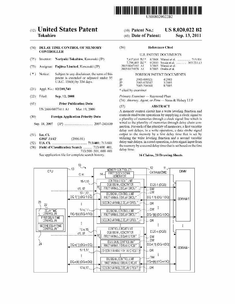
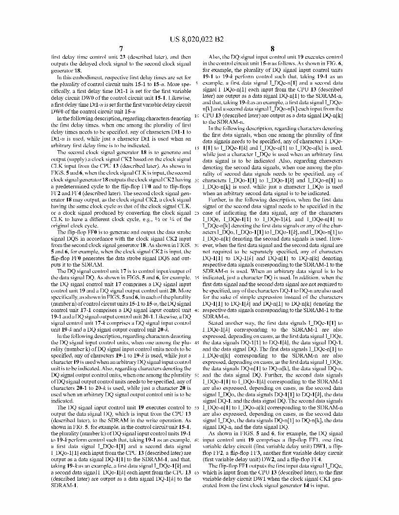
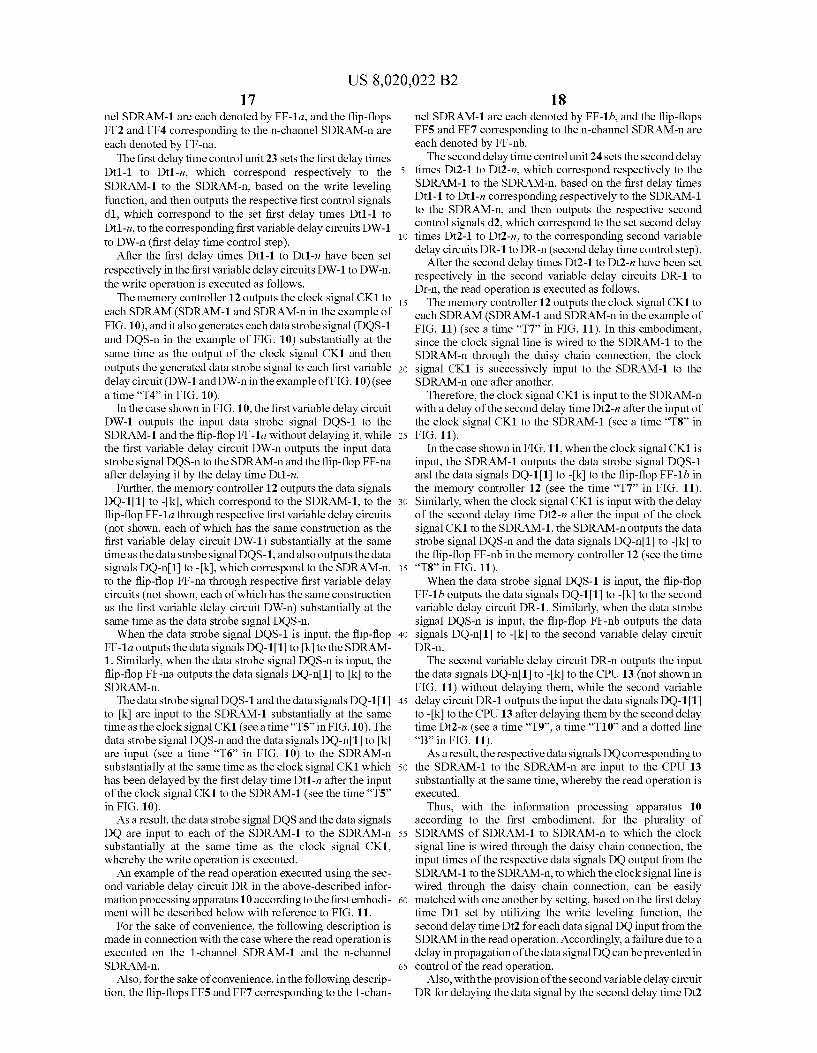
10 ^-y MEMORY CONTROLLER -12 11 DIMM
14 FIRSICLOCKSIGNAL CK1Add!CMD GENERATOR
CONTROLCIRCUITUN ...DQSSIGNALGENERATOR. -- DQS-1 (DQS) FIRSTVARIABLEDELAY CIRCUI - DW DSOAORLIN --Dw
: FIRSTVARIABLEDELAY CIRCUIT.L. DQ-11 (DQ-1-DQ) SDRAM1 * 22 SECONDVARIABLEDELAY CIRCUI-LDR
DELAYTIME 17-k, 17 DSIGNALCONTROLUNI-DW CONTROLUNT DQ-1K (DQ-1:DQ). FIRSTVARIABLEDELAY CIRCUIT; DQ-1(k)(DQ-1:DQ)
FIRSTDELAYTIME | N lili, CONTROLUNT | | | | | ESEUUNLVARIABLEDELAY CIRCUI - SDR :
SECOND DELAYTIME CONTROLUNT
DQS-n (DQS) 1 d1, d2 - - - - - - - - - - - - - - - - - - - -
FIRSTVARABLEDELAY CIRCUIT-L DW T. DW
24 DQ-n1 (DQ-n:DQ) DQ-n1 (DQ-n:DQ) ------itics: D SDRAM-n SECOND WARIABLEDELAY CIRCUIT is - DR
DOSIGNALCONTROLUNT - P. DQ-nk (DQ-n:DQ) FIRSTWARIABLEDELAY CIRCUI DQ-nk (DQ-n:DQ)
US 8,020,022 B2 Sheet 1 of 20 Sep. 13, 2011 U.S. Patent
rar -
LHW CIELIV TEH
}}ETTO?HINOO ÅèJOWIEW
US 8,020,022 B2 Sheet 2 of 20 Sep. 13, 2011 U.S. Patent
| 6
LHV CEIWTH H Z "SO|-
HETTO}]] NOO ÅèHOWE'W 06
US 8,020,022 B2 Sheet 3 of 20 Sep. 13, 2011 U.S. Patent
| 6
LHV CEI 1V/TEPH 9. "SO|-
06
US 8,020,022 B2 Sheet 4 of 20 Sep. 13, 2011 U.S. Patent
»– – – – – – – – – – –
US 8,020,022 B2 Sheet 5 of 20 Sep. 13, 2011 U.S. Patent
(GOOTIII)

US 8,020,022 B2 Sheet 7 of 20 Sep. 13, 2011 U.S. Patent
||
- ? -+ - - - - -TÕ???????? (SOG) U-SOO
US 8,020,022 B2 Sheet 8 of 20 Sep. 13, 2011 U.S. Patent
US 8,020,022 B2 Sheet 9 of 20 Sep. 13, 2011 U.S. Patent
00:00,00 ~ || 'X-/|
*
US 8,020,022 B2 Sheet 10 of 20 Sep. 13, 2011 U.S. Patent
| |
(SÒQ) u-SÖG
020,022 B2 9 US 8 Sheet 12 of 20 . 13, 2011 Sep . Patent
| e6)

US 8,020,022 B2 Sheet 16 of 20 Sep. 13, 2011 U.S. Patent
(NIC)Z-NI
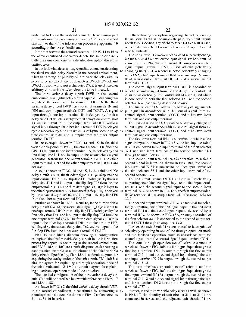
U.S. Patent Sep. 13, 2011 Sheet 17 of 20 US 8,020,022 B2
FIG. 18A
33-1 32-2 31
FIG. 18B FIG. 18C
33-1 32-2 31 33-1 32-2 31
OUT-1
020,022 B2 9 US 8 Sheet 18 of 20 2011 Sep. 13 Patent U.S.
e6, e6,

US 8,020,022 B2 Sheet 20 of 20 Sep. 13, 2011 U.S. Patent
(NIO) Z-NI

US 8,020,022 B2 1.
DELAYTIME CONTROL OF MEMORY CONTROLLER
CROSS-REFERENCE TO RELATED APPLICATIONS
This application is related to and claims priority to Japa nese patent application no. 2007-241610 filed on Sep. 18. 2007, in the Japan Patent Office, and incorporated by refer ence herein.
BACKGROUND
1. Field The memory control circuit, delay time control device, and
delay time control method relate to a technique for control ling read/write operations for a plurality of memories to which a clock signal line is wired through the daisy chain connection, as in, e.g., a DDR3 memory interface, by Supply ing a clock signal through the clock signal line.
2. Description of the Related Art Recently, the DDR3 (Double Data Rate 3) memory inter
face has been standardized as standards of a DRAM (Dy namic Random Access Memory) by JEDEC (Joint Electron Device Engineering Council) (see, e.g., JDEC STANDARD (JESD79-3; DDR3 SDRAM Standard). Unlike the hitherto practiced DDR (Double Data Rate) memory interface and DDR2 (Double Data Rate 2) memory interface (see, e.g., Japanese Laid-open Patent Publication No. 2003-99321, No. 2005-78547, and No. 2005-209168), the DDR3 memory interface employs fly-by topology for connection between a memory controller and a DIMM (Dual Inline Memory Mod ule).
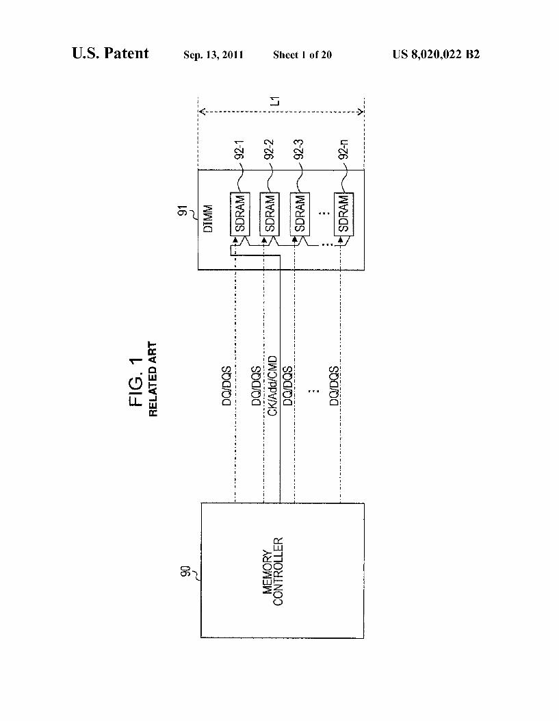
FIG. 1 is a block diagram showing a configuration example of the recently proposed DDR3 memory interface, and FIG.2 is a block diagram for explaining a write leveling operation in the DDR3 memory interface. As shown in FIG. 1, for example, the fly-by topology is
configured such that a signal line for each of a clock signal CK, an address signal Add and a command signal CMD is wired from a memory controller 90 to a plurality (number n) of SDRAMs (Synchronous Dynamic Random Access Memories) 92-1 to 92-n (n is a natural number of 2 or more) on a DIMM module 91 through the daisy chain connection. On the other hand, data signal lines for data signals DQ and data strobe signals DQS are wired from the memory control ler 90 to the plurality of SDRAMs 92-1 to 92-n on the DIMM module 91, respectively.
In the following description, regarding characters denoting the SDRAMs, when one among the plurality of SDRAMs needs to be specified, any of characters 92-1 to 92-n is used, while a character 92 is used when an arbitrary SDRAM is to be indicated.
Also, regarding characters denoting the data signals, when one among the plurality of data signals needs to be specified, any of characters DQ-1 to DQ-n is used, while a character DQ is used when an arbitrary data signal is to be indicated.
Further, regarding characters denoting the data strobe Sig nals, when one among the plurality of data strobe signals needs to be specified, any of characters DQS-1 to DQS-n is used, while a character DQS is used when an arbitrary data strobe signal is to be indicated.
Thus, in the DDR3 memory interface, because the clock signal line for the clock signal CK is wired to the plurality of SDRAMs 92-1 to 92-n through the daisy chain connection and a propagation delay is generated, the clock signal CK output from the memory controller 90 cannot reach all the
10
15
25
30
35
40
45
50
55
60
65
2 SDRAMs 92-1 to 92-n at the same time. According to the JEDEC standards, for example, a length L1 of outer dimen Sion of the DIMM module 91 is determined to be 133 mm. Assuming a data transmission speed to be 7 pS/mm, therefore, a difference of about 1 ns is generated in arrival time of the clock signal CK between the SDRAM 92-1 disposed at one end and the SDRAM 92-n disposed at the other end of the DIMM module 91 in the lengthwise direction thereof (namely, 7 ps/mmx133 mm=931 ps).
For that reason, according to the JEDEC standards, it is specified to employ the write leveling function in the DDR3 memory interface. The term “write leveling function” refers to the function of
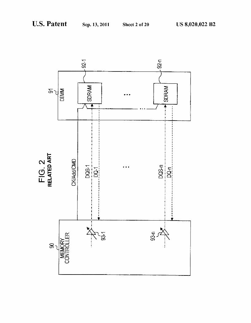
sampling the clock signal CK by using the data strobe signal DQS output from the memory controller 90, detecting the phase relationship between the data strobe signal DQS and the clock signal CK, and adjusting (compensating) a delay time of the data strobe signal DQS. The write leveling func tion is realized, as shown in FIG. 2, by incorporating variable delay circuits 93-1 to 93-n, which can change respective delay times of the data strobe signals DQS-1 to DQS-n, in the memory controller 90 corresponding to the plurality of SDRAMs 92-1 to 92-n, respectively.
In the following description, regarding characters denoting the delay circuits, when one among the plurality of delay circuits needs to be specified, any of characters 93-1 to 93-n is used, while a character 93 is used when an arbitrary delay circuit is to be indicated. More specifically, for the data strobe signals DQS-1 to
DQS-n output respectively to the plurality of SDRAMs 92-1 to 92-n to which the clock signal line is wired through the daisy chain connection, a CPU (Central Processing Unit, not shown) sets respective delay times t1-1 to t1-n based on the data signals DQ-1 to DQ-n output from the plurality of SDRAMs 92-1 to 92-n so that the data strobe signals DQS-1 to DQS-n are adjusted to be input respectively to the plurality of SDRAMs 92-1 to 92-n substantially at the same time as the clock signal CK for each SDRAM.
In other words, for example, at the time of completion of the write leveling, the data strobe signals DQS are delayed through the respective delay times t1-1 to t1-n in the delay circuits 93-1 to 93-n which correspond to the SDRAMs 92-1 to 92-n on the DIMM module 91, respectively, whereby the data strobe signal DQS and the clock signal CK are input in phase to each of the SDRAMs 92-1 to 92-n.
Thus, in the DDR3 memory interface, the difference in the delay time caused in the write operations between the memory controller 90 and the plurality of SDRAMs 92 is adjusted by employing the write leveling function.
Additionally, in the above-described case, the delay times t1-1 to t1-n are not equal to each other because the clock signal CK is input to the SDRAMs 92-1 to 92-n via the clock signal line through the daisy chain connection.
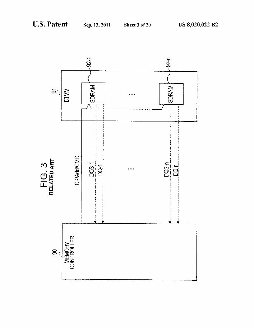
Although, the DDR3 memory interface compensates the arrival time when the data strobe signals DQS-1 to DQS-n arrive at the SDRAMs 92-1 to 92-n in the write operations according to the JEDEC standards as described above, com pensations of the signal arrival time in read operations are not provided with the JEDEC standards.
FIG. 3 is a block diagram explaining the read operation of the conventional DDR3 memory interface. The SDRAMs 92-1 though92-n output data signals DQ-1
though DQ-n and the data strobe signals DQS-1 through DQS-n to the memory controller 90 on receiving the clock signal CK output from the memory controller 90 via the data signal line in the daisy chain connection in the read operation as shown in FIG. 3.
US 8,020,022 B2 3
Therefore, the data signal DQ-n and the data strove signal DQS-n output from the SDRAM 92-n to which the clock signal CK is input lastly arrives at the memory controller 90 approximately 1 ns after the data signal DQ-1 and the data strobe signal DQS-1 output from the SDRAM92-1 to which the clock signal CK is input firstly where the data transmis sion speed is 7 pS/mm as the case described above. 7 pS/mmx 133 mm=931 ps. The delay on the order of 1 ns will become greater than a
typical data period of the DDR3 memory interface, at mini mum 0.625 ns, so that the delay may affect in reading data from the SDRAM 92.
SUMMARY
A memory control circuit having a write leveling function and controlling read/write operations by Supplying a clock signal to a plurality of memories through a clock signal line which is wired to the plurality of memories through daisy chain connection is comprising, for each of the plurality of memories, a first variable delay unit for delaying, in the write operation, a data strobe signal output to the memory by a first delay time that is set by utilizing the write leveling function and a second variable delay unit for delaying, in the read operation, a data signal input from the memory by a second delay time that is set based on the first delay time.
Additional objects and advantages of the embodiment will be set forth in part in the description which follows, and in part will be obvious from the description, or may be learned by practice of the embodiment. The object and advantages of the embodiment will be realized and attained by the elements and combinations particularly pointed out in the appended claims.
It is to be understood that both the foregoing general description and the following detailed description are exem plary and explanatory only and are not restrictive of the embodiment, as claimed.
These together with other aspects and advantages which will be subsequently apparent, reside in the details of con struction and operation as more fully hereinafter described and claimed, reference being had to the accompanying draw ings forming a part hereof, wherein like numerals refer to like parts throughout.
BRIEF DESCRIPTION OF THE DRAWINGS
FIG. 1 is a block diagram showing a configuration example of the known DDR3 memory interface;
FIG. 2 is a block diagram for explaining a write leveling operation in the known DDR3 memory interface;
FIG.3 is a block diagram for explaining a read operation in the known DDR3 memory interface;
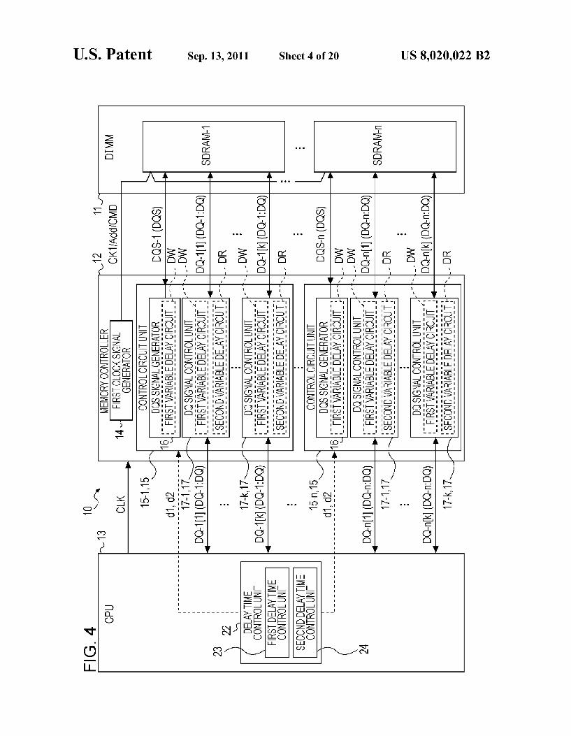
FIG. 4 is a block diagram showing a configuration example of an information processing apparatus according to a first embodiment;
FIG.5 is a block diagram showing a configuration example of a circuit of a memory controller, which corresponds to SDRAM-1, in the information processing apparatus accord ing to the first embodiment;
FIG. 6 is a block diagram showing a configuration example of a circuit of the memory controller, which corresponds to SDRAM-n, in the information processing apparatus accord ing to the first embodiment;
FIG. 7 is an explanatory diagram for explaining the write leveling function of a first delay time control unit in the information processing apparatus according to the first embodiment;
10
15
25
30
35
40
45
50
55
60
65
4 FIG. 8 is a block diagram for explaining calculation for
mulae used to determine a first delay time in the first delay time control unit of the information processing apparatus according to the first embodiment;
FIG. 9 is a block diagram for explaining the calculation formulae used to determine the first delay time in the first delay time control unit of the information processing appa ratus according to the first embodiment;
FIG. 10 is an explanatory diagram for explaining a write operation using a first variable delay circuit in the information processing apparatus according to the first embodiment;
FIG. 11 is an explanatory diagram for explaining a read operation using a second variable delay circuit in the infor mation processing apparatus according to the first embodi ment;
FIG. 12 is a circuit diagram showing a portion of the memory controller, which corresponds to the SDRAM-1, in the information processing apparatus according to a modifi cation of the first embodiment;
FIG. 13 is a circuit diagram showing a portion of the memory controller, which corresponds to the SDRAM-n, in the information processing apparatus according to the modi fication of the first embodiment;
FIG. 14 is a circuit diagram showingaportion of a memory controller, which corresponds to SDRAM-1, in an informa tion processing apparatus according to a second embodiment;
FIG. 15 is a circuit diagram showing a portion of the memory controller, which corresponds to SDRAM-n, in the information processing apparatus according to the second embodiment;
FIG. 16 is a diagram for explaining the function of a third variable delay circuit of the memory controller in the infor mation processing apparatus according to the second embodi ment;
FIG. 17 is a block diagram showing a configuration example of the third variable delay circuit in the information processing apparatus according to the second embodiment;
FIGS. 18A to 18C are circuit diagrams each showing a configuration example of a unit circuit of the third variable delay circuit in the information processing apparatus accord ing to the second embodiment;
FIG. 19 is a circuit diagram showing a portion of the memory controller, which corresponds to the SDRAM-1, in the information processing apparatus according to a modifi cation of the second embodiment;
FIG. 20 is a circuit diagram showing a portion of the memory controller, which corresponds to the SDRAM-n, in the information processing apparatus according to the modi fication of the second embodiment; and
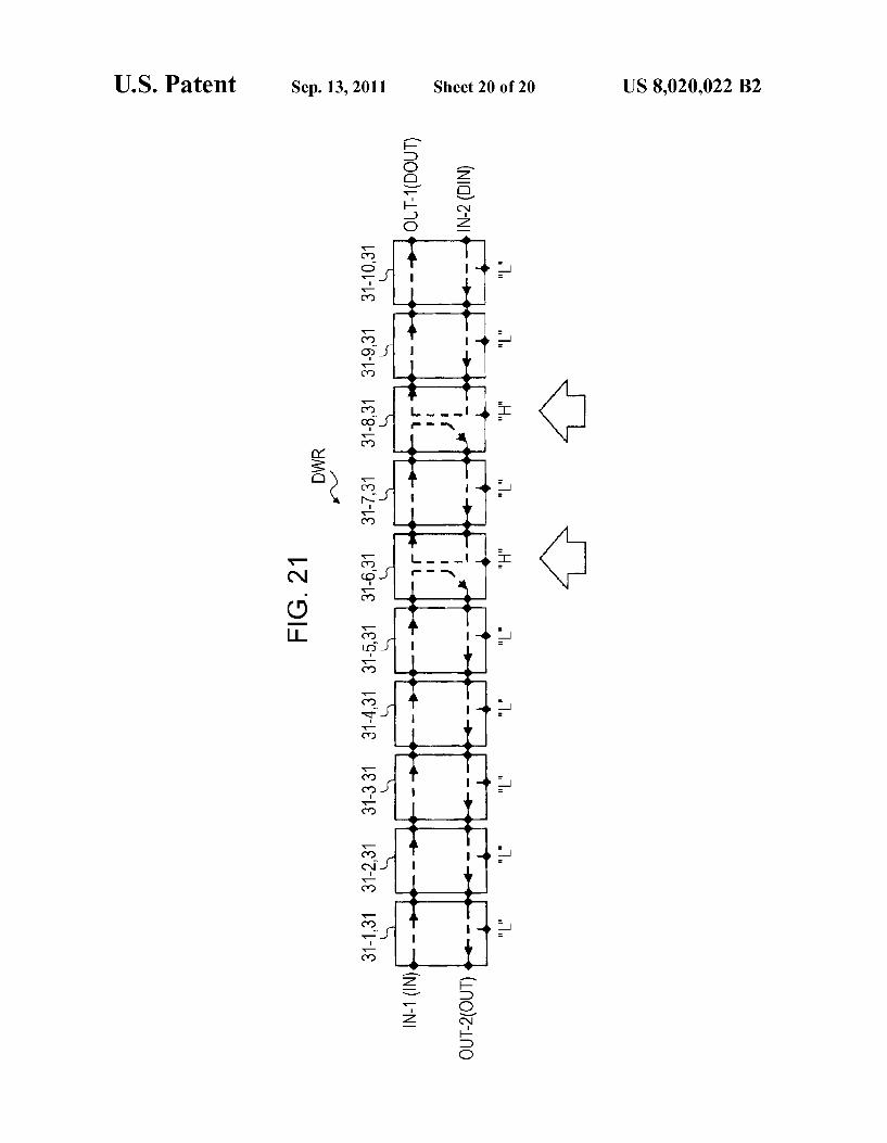
FIG. 21 is a block diagram for explaining another example of use of the third variable delay circuit in the information processing apparatus according to the second embodiment.
DETAILED DESCRIPTION OF THE PREFERRED EMBODIMENTS
Embodiments will be described below with reference to the drawings.
1 First Embodiment
FIG. 4 is a block diagram showing a configuration example of an information processing apparatus according to a first embodiment, FIG. 5 is a block diagram showing a configu ration example of a circuit of a memory controller, which corresponds to SDRAM-1, in the information processing apparatus, and FIG. 6 is a block diagram showing a configu
US 8,020,022 B2 5
ration example of a circuit of the memory controller, which corresponds to SDRAM-n, in the information processing apparatus. As shown in FIG. 4, an information processing apparatus
(delay time control device) 10 according to the first embodi ment is constituted as a computer comprising a DIMM (Dual Inline Memory Module) 11, a memory controller (memory control circuit) 12, and a CPU (Central Processing Unit) 13. The DIMM 11 is a memory module incorporating a plu
rality of memories therein. In the first embodiment, as shown in FIG. 4, the DIMM 11 includes a plurality (number n) of SDRAMs (Synchronous DRAMs (Dynamic Random Access Memories)), i.e., SDRAM-1 to SDRAM-n (n is a natural number of 2 or more). Also, “n” represents the number of channel (ch), but for the sake of simplicity, only the SDRAM-1 and SDRAM-n are illustrated in FIG. 4. It is to be noted that SDRAM itself is the known technique and a detailed description thereof is omitted here.
In the following description, regarding characters denoting the SDRAMs, when one among the plurality of SDRAMs needs to be specified, any of 1 to n is suffixed to SDRAM along with '-', while just SDRAM is used when an arbitrary SDRAM is to be indicated.
Further, in the first embodiment, fly-by topology is employed for wiring between the memory controller 12 and the plural SDRAMs of SDRAM-1 to SDRAM-n.
The term “fly-by topology” refers the daisy chain connec tion is used as part of the wiring between the memory con troller 12 and the plural SDRAMs of SDRAM-1 to SDRAM l.
In the first embodiment, therefore, a clock signal line for outputting (supplying) a clock signal CK1 generated by a first clock signal generator 14 (described later) is wired to the SDRAM-1 to the SDRAM-n through the daisy chain connec tion. Stated another way, as shown in FIG. 4, the clock signal line connected to the first clock signal generator 14 is con nected to the SDRAM-1 to the SDRAM-n in series one after another. As with the clock signal line, other signal lines for outputting an address signal Addanda command signal CMD are also each connected to the SDRAM-1 to the SDRAM-n through the daisy chain connection.
Data signal line for interconnecting the memory controller 12 and the plural SDRAMs of SDRAM-1 to SDRAM-n are connected from the memory controller 12 respectively to the plural SDRAMs of SDRAM-1 to SDRAM-n in parallel. In the exemplary circuit diagram shown in FIG. 5, one DQS signal line (data signal line) for transmitting the data strobe signal DQS and a number k (k is a natural number of 2 or more) of DQ signal lines (data signal lines) for transmitting data signals DQ are connected from the memory controller 12 to each of the plural SDRAMs of SDRAM-1 to SDRAM-n in parallel. Further, those data signal lines are wired in lengths equal to one another (i.e. in the same length). In other words, the plurality of data signal lines connecting the memory con troller 12 and the plural SDRAMs of SDRAM-1 to SDRAM-n have the same length. The memory controller 12 is a DDR3 (Double Data Rate 3)
memory interface for controlling read/write operations by Supplying, through the clock signal line, the clock signal CK1 to the plural SDRAMs of SDRAM-1 to SDRAM-n to which the clock signal line is wired through the daisy chain connec tion. As shown in FIG. 4, by way of example, the memory controller 12 comprises the first clock signal generator 14 and a plurality of control circuit units 15-1 to 15-n.
In addition, the memory controller 12 has the write leveling function. Details of the write leveling function will be described later.
10
15
25
30
35
40
45
50
55
60
65
6 The plural control circuit units 15-1 to 15-in are constituted
corresponding to the plural SDRAMs of SDRAM-1 to SDRAM-n, respectively. In other words, as shown in FIG.4, the memory controller 12 includes, for example, the control circuit unit 15-1 corresponding to SDRAM-1 and the control circuit unit 15-in corresponding to SDRAM-n.
In the following description, regarding characters denoting the control circuit units, when one among the plurality of control circuit units needs to be specified, any of 1 to n is suffixed to a character 15 along with “-”, while just the char acter 15 is used when an arbitrary control circuit unit is to be indicated.
Also, for the sake of simplicity, only the control circuit unit 15-1 and the control circuit unit 15-in are illustrated in the drawings. The first clock signal generator 14 generates and outputs
the clock signal CK1 having a predetermined cycle based on a clock signal CLK input from a CPU13 (described later). As shown in FIGS. 5 and 9, for example, the first clock signal generator 14 outputs the clock signal CK1 to not only the DIMM 11 (SDRAM-1 to SDRAM-n), but also to the plural control circuit units 15-1 to 15-in through the clock signal lines. The first clock signal generator 14 may output, as the clock signal CK1, a clock signal having the same clock cycle as that of the clock signal CLK, or a clock signal produced by converting the clock signal CLK to have a different clock cycle, e.g., /2 or 4 of the original clock cycle. The control circuit unit 15 is to control input/output of the
data strobe signal DQS and the data signals DQ. As shown in FIGS. 4 to 6, for example, the control circuit unit 15 com prises a DQS signal generator 16, a number k (k is a natural number of 2 or more) of DQ signal control units 17-1 to 17-k, and a logical sum circuit OR (see FIGS. 5 and 6).
In the following description, regarding characters denoting the DQ signal control units, when one among the DQ signal control units needs to be specified, any of 1 to k is suffixed to a character 17 along with “-”, while just the character 17 is used when an arbitrary DQ signal control unit is to be indi cated.
Also, for the sake of simplicity, only the DQ signal control unit 17-1 and the DQ signal control units 17-kare illustrated in the drawings. The DQS signal generator 16 is to generate the data strobe
signal DQS and is included in each control circuit unit 15 in a one-to-one relation. As shown in FIG. 5, for example, the control circuit unit 15-1 generates a data strobe signal DQS-1 and outputs it to SDRAM-1. Also, as shown in FIG. 6, the control circuit unit 15-in generates a data strobe signal DQS-n and outputs it to SDRAM-n.
In the following description, regarding characters denoting the data strobe signals, when one among the plurality of data strobe signals needs to be specified, any of characters DQS-1 to DQS-n is used, while just a character DQS is used when an arbitrary data strobe signal is to be indicated. As shown in FIGS. 5 and 6, for example, the DQS signal
generator 16 comprises a first variable delay circuit (first variable delay unit) DW0, a second clock signal generator 18, and a flip-flop FF0. The first variable delay circuit DW0 is to delay the clock
signal CLK, which is input from the CPU13 (described later), in accordance with a first control signal d1 from a first delay time control unit 23 (described later), and to output the delayed clock signal. For example, the first variable delay circuit DW0 delays the clock signal CLK, which is input from the CPU 13 (described later), by a first delay time set by the
US 8,020,022 B2 7
first delay time control unit 23 (described later), and then outputs the delayed clock signal to the second clock signal generator 18.
In this embodiment, respective first delay times are set for the plurality of control circuit units 15-1 to 15-in. More spe cifically, a first delay time Dt1-1 is set for the first variable delay circuit DW0 of the control circuit unit 15-1. Likewise, a first delay time Dt1-n is set for the first variable delay circuit DWO of the control circuit unit 15-in.
In the following description, regarding characters denoting the first delay times, when one among the plurality of first delay times needs to be specified, any of characters Dt1-1 to Dt1-n is used, while just a character Dt1 is used when an arbitrary first delay time is to be indicated. The second clock signal generator 18 is to generate and
output (Supply) a clock signal CK2 based on the clock signal CLK input from the CPU 13 (described later). As shown in FIGS. 5 and 6, when the clock signal CLK is input, the second clock signal generator 18 outputs the clock signal CK2 having a predetermined cycle to the flip-flop FF0 and to flip-flops FF2 and FF4 (described later). The second clock signal gen erator 18 may output, as the clock signal CK2, a clock signal having the same clock cycle as that of the clock signal CLK, or a clock signal produced by converting the clock signal CLK to have a different clock cycle, e.g., /2 or 4 of the original clock cycle. The flip-flop FF0 is to generate and output the data strobe
signal DQS in accordance with the clock signal CK2 input from the second clock signal generator 18. As shown in FIGS. 5 and 6, for example, when the clock signal CK2 is input, the flip-flop FF0 generates the data strobe signal DQS and out puts it to the SDRAM.
The DQ signal control unit 17 is to control input/output of the data signal DQ. As shown in FIGS. 5 and 6, for example, the DQ signal control unit 17 comprises a DQ signal input control unit 19 and a DQ signal output control unit 20. More specifically, as shown in FIGS. 5 and 6, in each of the plurality (number n) of control circuit units 15-1 to 15-in, the DQ signal control unit 17-1 comprises a DQ signal input control unit 19-1 and a DQ signal output control unit 20-1. Likewise, a DQ signal control unit 17-k comprises a DQ signal input control unit 19-k and a DQ signal output control unit 20-k.
In the following description, regarding characters denoting the DQ signal input control units, when one among the plu rality (number k) of DQ signal input control units needs to be specified, any of characters 19-1 to 19-k is used, while just a character 19 is used when an arbitrary DQ signal input control unit is to be indicated. Also, regarding characters denoting the DQ signal output control units, when one among the plurality of DQ signal output control units needs to be specified, any of characters 20-1 to 20-k is used, while just a character 20 is used when an arbitrary DQ signal output control unit is to be indicated. The DQ signal input control unit 19 executes control to
output the data signal DQ, which is input from the CPU 13 (described later), to the SDRAM in the write operation. As shown in FIG. 5, for example, in the control circuit unit 15-1, the plurality (numberk) of DQ signal input control units 19-1 to 19-k perform control such that, taking 19-1 as an example, a first data signal I DQe-11 and a second data signal I DQo-11 each input from the CPU 13 (described later) are output as a data signal DQ-11 to the SDRAM-1, and that, taking 19-kas an example, a first data signal I DQe-1k and a second data signal I DQo-1R each input from the CPU 13 (described later) are output as a data signal DQ-1R to the SDRAM-1.
5
10
15
25
30
35
40
45
50
55
60
65
8 Also, the DQ signal input control unit 19 executes control
in the control circuit unit 15-in as follows. As shown in FIG. 6, for example, the plurality of DQ signal input control units 19-1 to 19-k perform control such that, taking 19-1 as an example, a first data signal I DQe-n1 and a second data signal I DQo-n1 each input from the CPU 13 (described later) are output as a data signal DQ-n1 to the SDRAM-n, and that, taking 19-kas an example, a first data signal I DQe nk and a second data signal I DQo-nk each input from the CPU 13 (described later) are output as a data signal DQ-nk to the SDRAM-n.
In the following description, regarding characters denoting the first data signals, when one among the plurality of first data signals needs to be specified, any of characters I DQe 11 to I DQe-1R and I DQe-n1 to I DQe-nk is used, while just a character I DQe is used when an arbitrary first data signal is to be indicated. Also, regarding characters denoting the second data signals, when one among the plu rality of second data signals needs to be specified, any of characters I DQo-11 to I DQo-1 k and I DQo-n1 to I DQo-nk is used, while just a character I DQo is used when an arbitrary second data signal is to be indicated.
Further, in the following description, when the first data signal or the second data signal needs to be specified in the case of indicating the data signal, any of the characters I DQe, I DQe-11 to I DQe-1R, and I DQe-n1 to I DQe-nk denoting the first data signals or any of the char acters I DQo, I DQo-11 to I DQo-1 k, and I DQo-n1 to I DQo-nk denoting the second data signals is used. How ever, when the first data signal and the second data signal are not required to be separately specified, any of characters DQ-11 to DQ-1 k and DQ-n1 to DQ-nk denoting respective data signals corresponding to the SDRAM-1 to the SDRAM-n is used. When an arbitrary data signal is to be indicated, just a character DQ is used. In addition, when the first data signal and the second data signal are not required to be specified, any of the characters DQ-1 to DQ-nare also used for the sake of simple expression instead of the characters DQ-11 to DQ-1k and DQ-n1 to DQ-nk denoting the respective data signals corresponding to the SDRAM-1 to the SDRAM-n.
Stated another way, the first data signals I DQe-11 to I DQe-1R corresponding to the SDRAM-1 are also expressed, depending on cases, as the first data signal I DQe, the data signals DQ-11 to DQ-1R, the data signal DQ-1, and the data signal DQ. The first data signals I DQe-n1 to I DQe-nk corresponding to the SDRAM-n are also expressed, depending on cases, as the first data signal I DQe, the data signals DQ-n1 to DQ-nk, the data signal DQ-n, and the data signal DQ. Further, the second data signals I DQo-11 to I DQo-1 k corresponding to the SDRAM-1 are also expressed, depending on cases, as the second data signal I DQo, the data signals DQ-11 to DQ-1 k, the data signal DQ-1, and the data signal DQ. The second data signals I DQo-n1 to I DQo-nk corresponding to the SDRAM-n are also expressed, depending on cases, as the second data signal I DQo, the data signals DQ-n1 to DQ-nk, the data signal DQ-n, and the data signal DQ. As shown in FIGS. 5 and 6, for example, the DQ signal
input control unit 19 comprises a flip-flop FF1, one first variable delay circuit (first variable delay unit) DW1, a flip flop FF2, a flip-flop FF3, another first variable delay circuit (first variable delay unit) DW2, and a flip-flop FF4. The flip-flop FF1 outputs the first input data signal I DQe,
which is input from the CPU 13 (described later), to the first variable delay circuit DW1 when the clock signal CK1 gen erated from the first clock signal generator 14 is input.
US 8,020,022 B2
The first variable delay circuit DW1 is a digital delay circuit for delaying the first input data signal I DQe, which is input from the flip-flop FF1, in accordance with a first control signal d1 from the first delay time control unit 23 (described later), and for outputting the delayed first input data signal I DQe to the flip-flop FF2. For example, the first variable delay circuit DW1 delays the first input data signal I DQe, which is input from the flip-flop FF1, by a first delay time Dt1 set by the first delay time control unit 23 (described later) and then outputs the delayed first input data signal I DQe to the flip-flop FF2. The flip-flop FF2 outputs the first input data signal I DQe,
which is input from the first variable delay circuit DW1, to the SDRAM through a selector 21 when the clock signal CK2 generated from the second clock signal generator 18 is input. The flip-flop FF3 outputs the second input data signal
I DQo, which is input from the CPU 13 (described later), to the first variable delay circuit DW2 when the clock signal CK1 generated from the first clock signal generator 14 is input. The first variable delay circuit DW2 is a digital delay
circuit for delaying the second input data signal I DQo. which is input from the flip-flop FF3, in accordance with the first control signal d1 from the first delay time control unit 23 (described later), and for outputting the delayed second input data signal I DQo to the flip-flop FF4. For example, the first variable delay circuit DW2 delays the second input data sig nal I DQo, which is input from the flip-flop FF3, by the first delay time Dt1 set by the first delay time control unit 23 (described later) and then outputs the delayed second input data signal I DQo to the flip-flop FF4.
In this embodiment, it is assumed that the same first delay time Dt1 is set for each of the plural SDRAMs of SDRAM-1 to SDRAM-n. More specifically, a first delay time Dt1-1 is set for the three first variable delay circuits DW0, DW1 and DW2 which are included in the control circuit unit 15-1 shown in FIG. 5. Likewise, a first delay time Dt1-n is set for the three first variable delay circuits DW0, DW1 and DW2 which are included in the control circuit unit 15-in shown in FIG. 6.
In the following description, regarding characters denoting the first variable delay circuits, when one among the plurality of first variable delay circuits needs to be specified, any of characters DW0, DW1 and DW2 is used, while just a char acter DW is used when an arbitrary first variable delay circuit is to be indicated.
Further, in the following description, a character DW-1 is also used to indicate the first variable delay circuit corre sponding to the 1-channel SDRAM-1 for the sake of express ing the correlation. Likewise, a character DW-n is also used to indicate the first variable delay circuit corresponding to the n-channel SDRAM-n. The flip-flop FF4 outputs the second input data signal
I DQo, which is input from the first variable delay circuit DW2, to the SDRAM through the selector 21 when the clock signal CK2 generated from the second clock signal generator 18 is input. The DQ signal output control unit 20 executes control to
output the data signal DQ, which is input from the SDRAM, to the CPU 13 (described later) in the read operation. As shown in FIG. 5, for example, in the control circuit unit 15-1, the plurality of DQ signal output control units 20-1 to 20-k perform control Such that, taking 20-1 as an example, the data signal DQ-11 input from the SDRAM-1 is output as a third data signal O DQe-11 and a fourth data signal O DQo-11 to the CPU 13 (described later), and that, taking 20-k as an example, the data signal DQ-1 k input from the SDRAM-1 is
5
10
15
25
30
35
40
45
50
55
60
65
10 output as a third data signal O DQe-1k and a fourth data signal O DQo-1 k to the CPU 13 (described later).
Also, the DQ signal output control unit 20 executes control in the control circuit unit 15-in as follows. As shown in FIG. 6, for example, the plurality of DQ signal output control units 20-1 to 20-k perform control such that, taking 20-1 as an example, the data signal DQ-n1 input from the SDRAM-n is output as a third data signal O DQe-n1 and a fourth data signal O DQo-n1 to the CPU13 (described later), and that, taking 20-kas an example, the data signal DQ-nk input from the SDRAM-n is output as a third data signal O DQe-nk and a fourth data signal O DQo-nk to the CPU 13 (de scribed later).
In the following description, regarding characters denoting the third data signals, when one among the plurality of third data signals needs to be specified, any of characters O DQe 11 to O DQe-1K and O DQe-n1 to O DQe-nk is used, while just a character O DQe is used when an arbitrary third data signal is to be indicated. Also, regarding characters denoting the fourth data signals, when one among the plural ity of fourth data signals needs to be specified, any of char acters O DQo-11 to O DQo-1 k and O DQo-n1 to O DQo-nk is used, while just a character O DQo is used when an arbitrary fourth data signal is to be indicated.
Further, in the following description, when the third data signal and the fourth data signal needs to be separately speci fied in the case of indicating the data signal, any of the characters O DQe, O DQe-11 to O DQe-1R, and O DQe-n1 to O DQe-nk denoting the third data signals or any of the characters O DQo, O DQo-11 to O DQo-1 Rand O DQo-n1 to O DQo-nk denoting the fourth data signals is used. However, when the third data signal and the fourth data signal are not required to be separately specified, any of characters DQ-11 to DQ-1R and DQ-n1 to DQ-n k denoting respective data signals corresponding to the SDRAM-1 to the SDRAM-n is used. When an arbitrary data signal is to be indicated, just a character DQ is used. In addition, when the third data signal and the fourth data signal are not required to be separately specified, any of the charac ters DQ-1 to DQ-n are also used for the sake of simple expression instead of the characters DQ-11 to DQ-1 k and DQ-n1 to DQ-nk denoting the respective data signals cor responding to the SDRAM-1 to the SDRAM-n.
Stated another way, the third data signals O DQe-11 to O DQe-1R corresponding to the SDRAM-1 are also expressed, depending on cases, as the third data signal O DQe, the data signals DQ-11 to DQ-1 K, the data signal DQ-1, and the data signal DQ. The third data signals O DQe n1 to O DQe-nk corresponding to the SDRAM-n are also expressed, depending on cases, as the third data signal O DQe, the data signals DQ-n1 to DQ-nk, the data signal DQ-n, and the data signal DQ. Further, the fourth data signals O DQo-11 to O DQo-1 k corresponding to the SDRAM-1 are also expressed, depending on cases, as the fourth data signal O DQo, the data signals DQ-11 to DQ-1 R, the data signal DQ-1, and the data signal DQ. The fourth data signals O DQo-n1 to O DQo-nk corresponding to the SDRAM-n are also expressed, depending on cases, as the fourth data signal O DQo, the data signals DQ-n1 to DQ-n k, the data signal DQ-n, and the data signal DQ. As shown in FIGS. 5 and 6, for example, the DQ signal
output control unit 20 comprises a flip-flop FF5, one second variable delay circuit (second variable delay unit) DR1, a flip-flop FF6, a flip-flop FF7, another second variable delay circuit (second variable delay unit) DR2, and a flip-flop FF8.
US 8,020,022 B2 11
The flip-flop FF5 outputs the third data signal O DQe, which is input from the SDRAM, to the second variable delay circuit DR1 when the data strobesignal DQS is input from the SDRAM. The second variable delay circuit DR1 is a digital delay
circuit for delaying the third data signal O DQe, which is input from the flip-flop FF5, in accordance with a second control signal d2 from the second delay time control unit 24 (described later), and for outputting the delayed third data signal O DQe to the flip-flop FF6. For example, the second variable delay circuit DR1 delays the third data signal O DQe, which is input from the flip-flop FF5, by a second delay time set by the second delay time control unit 24 (de scribed later) and then outputs the delayed third data signal O DQe to the flip-flop FF6.
In this embodiment, respective second delay times are set for the plurality of control circuit units 15-1 to 15-in. More specifically, a second delay time Dt2-1 is set for the second variable delay circuit DR1 of the control circuit unit 15-1. Likewise, a second delay time Dt2-n is set for the second variable delay circuit DR1 of the control circuit unit 15-n.
In the following description, regarding characters denoting the second delay times, when one among the plurality of second delay times needs to be specified, any of characters Dt2-1 to Dt2-n is used, while just a character Dt2 is used when an arbitrary second delay time is to be indicated. The flip-flop FF6 outputs the third data signal O DQe,
which is input from the second variable delay circuit DR1, to the CPU 13 (described later) when the clock signal CK1 generated from the first clock signal generator 14 is input.
The flip-flop FF7 outputs the fourth data signal O DQo, which is input from the SDRAM, to the second variable delay circuit DR2 when the data strobesignal DQS is input from the SDRAM. The second variable delay circuit DR2 is a digital delay
circuit for delaying the fourth data signal O DQo, which is input from the flip-flop FF7, in accordance with the second control signal d2 from the second delay time control unit 24 (described later), and for outputting the delayed fourth data signal O DQo to the flip-flop FF8. For example, the second variable delay circuit DR2 delays the fourth data signal O DQo, which is input from the flip-flop FF7, by the second delay time Dt2 set by the second delay time control unit 24 (described later) and then outputs the delayed fourth data signal O DQo to the flip-flop FF8.
In this embodiment, it is assumed that the same second delay time Dt2 is set for each of the plural SDRAMs of SDRAM-1 to SDRAM-n. More specifically, a second delay time Dt2-1 is set for the
two second variable delay circuits DR1 and DR2 which are included in the control circuit unit 15-1 shown in FIG. 5. Likewise, a second delay time Dt2-n is set for the two second variable delay circuits DR1 and DR2 which are included in the control circuit unit 15-in shown in FIG. 6.
In the following description, regarding characters denoting the second variable delay circuits, when one among the plu rality of second variable delay circuits needs to be specified, any of characters DR1 and DR2 is used, while just a character DR is used when an arbitrary second variable delay circuit is to be indicated.
Further, in the following description, a character DR-1 is also used to indicate the second variable delay circuit corre sponding to the 1-channel SDRAM-1 for the sake of express ing the correlation. Likewise, a character DR-n is also used to indicate the second variable delay circuit corresponding to the n-channel SDRAM-n.
10
15
25
30
35
40
45
50
55
60
65
12 The flip-flop FF8 outputs the fourth input data signal
O DQo, which is input from the second variable delay circuit DR2, to the CPU 13 (described later) when the clock signal CK1 generated from the first clock signal generator 14 is input. The logical Sum circuit OR outputs a response signal to the
CPU 13 (described later) in accordance with the third data signal O DQe and the fourth data signal O DQo when the write leveling function (described later) is employed. More specifically, as shown in FIG. 5, for example, when
the write leveling function (described later) is employed, the logical sum circuit OR included in the control circuit unit 15-1 operates such that a response signal O DQX-1 is output to the CPU 13 (described later) when any of the plurality of third data signals O DQe-11 to O DQe-1R corresponding to the SDRAM-1 and the plurality of fourth data signals O DQo-11 to O DQo-1 k corresponding to the SDRAM-1 is input.
Also, as shown in FIG. 6, for example, when the write leveling function (described later) is employed, the logical sum circuit OR included in the control circuit unit 15-in oper ates Such that a response signal O DQX-n is output to the CPU 13 (described later) when any of the plurality of third data signals O DQe-n1 to O DQe-nk corresponding to the SDRAM-n and the plurality of fourth data signals O DQo-n1 to O DQo-nk corresponding to the SDRAM-n is input.
In the following description, regarding characters denoting the response signals, when one among the plurality of response signals needs to be specified, any of characters O DQX-1 to O DQX-n is used, while just a character O DQX is used when an arbitrary response signal is to be indicated. The CPU 13 executes various kinds of numerical calcula
tions, information processing, equipment control, etc. in the information processing apparatus 10, and it functions as the delay time control unit 22 in this embodiment. Also, the CPU 13 includes a MAC (Media Access Control; not shown) and executes inputting/outputting of various signals (such as the data signals DQ, the clock signal CLK, and the response signal DQX) through the MAC. The delay time control unit 22 outputs a control signal for
setting respective delay times to the first variable delay circuit DW and the second variable delay circuit DR which are included in each of the control circuit units 15-1 to 15-in. As shown in FIG.4, the delay time control unit 22 comprises the first delay time control unit 23 and the second delay time control unit 24. The first delay time control unit 23 controls the first vari
able delay circuit DW, which is included in each of the control circuit units 15-1 to 15-in, to delay the data signal by the first delay time Dt1 based on the write leveling function, and it outputs the first control signal d1 for setting the first delay time Dt1. Also, in this embodiment, the first delay time con trol unit 23 sets, based on the write leveling function, the first delay times Dt1-1 to Dt1-n for the data strobe signals DQS-1 to DQS-n, which are output respectively to the plural SDRAMs of SDRAM-1 to SDRAM-n in the write operation.
Herein, the write leveling function refers to a function of adjusting (compensating) the data strobe signals DQS-1 to DQS-n so that they are input respectively to the plural SDRAMs of SDRAM-1 to SDRAM-n substantially at the same times as the clock signal CK1. The write leveling func tion is realized by setting the first delay times Dt1-1 to Dt1-n for the data strobe signals DQS-1 to DQS-n, which are output respectively to the plural SDRAMs of SDRAM-1 to SDRAM-n to which the clock signal line is wired through the

US 8,020,022 B2 13
daisy chain connection, corresponding to the data signals DQ-1 to DQ-n output from the SDRAM-1 to the SDRAM-n.
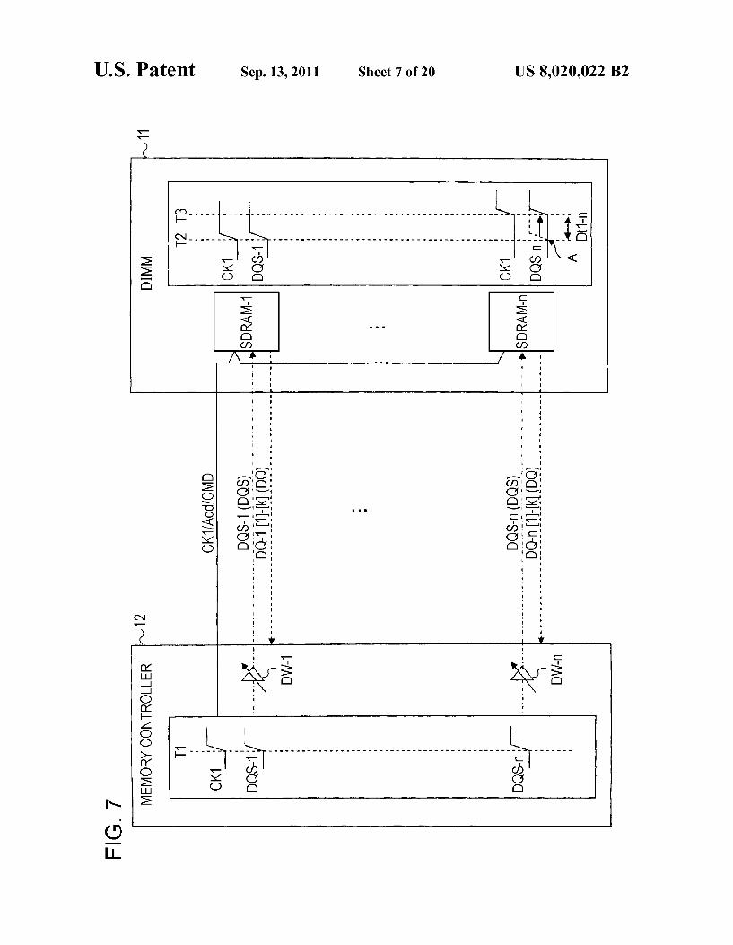
FIG. 7 is an explanatory diagram for explaining the write leveling function of the first delay time control unit in the information processing apparatus according to the first embodiment.
Regarding the case of setting the first delay times Dt1-1 to Dt1-n, which correspond respectively to the SDRAM-1 to the SDRAM-n, in the first delay time control unit 23 based on the write leveling function, the following description is made in connection with an example of setting the first delay time Dt1-1 corresponding to the 1-channel SDRAM-1 and the first delay time Dt1-n corresponding to the n-channel SDRAM-n, as shown in FIG. 7.
Also, each SDRAM (SDRAM-1 or SDRAM-n in the example shown in FIG. 7) outputs the data signal DQ (DQ-1 1 to -k and DQ-n1 to -k in the example shown in FIG. 7) to the memory controller 12 when the clock signal CK1 and the data strobe signal DQS (DQS-1 or DQS-n in the example shown in FIG. 7) are input to each SDRAM substantially at the same time.
First, the memory controller 12 outputs the clock signal CK1 to each SDRAM (SDRAM-1 or SDRAM-n in the example shown in FIG. 7) and also outputs the data strobe signal DQS (DQS-1 or DQS-n in the example shown in FIG. 7) to each SDRAM (SDRAM-1 or SDRAM-n in the example shown in FIG. 7) at the same time or substantially at the same time as the clock signal CK1 (see a time “T1 in FIG. 7).
For example, before the first delay time Dt1 is adjusted based on the write leveling function, as shown in FIG. 7, the clock signal CK1 and the data strobe signal DQS-1 are input to the 1-channel SDRAM-1 substantially at the same time (see a time “T2 in FIG. 7), while the clock signal CK1 is input (see a time “T3” in FIG.7) to the n-channel SDRAM-n with a delay of the time Dt1-n after the input of the data strobe signal DQS-n (see the time “T2 and a point “A” in FIG. 7).
In that case, for the 1-channel SDRAM-1, because the clock signal CK1 and the data strobe signal DQS-1 are input to the 1-channel SDRAM-1 substantially at the same time, the first delay time control unit 23 (not shown in FIG. 7) does not set the first delay time Dt1-1 for the data strobesignal DQS-1 corresponding to the first variable delay circuit DW-1 upon detecting that any of the data signals DQ-11 to -k from the 1-channel SDRAM-1 is input to the logical sum circuit OR-1 and the logical Sum circuit OR-1 outputs the response signal O DQX-1. On the other hand, for the n-channel SDRAM-n, the first
delay time Dt1-n corresponding to the data strobe signal DQS-n is set for the first variable delay circuit DW-nin match with the clock signal CK1 that is input (see the time “T3' in FIG. 7) to the n-channel SDRAM with a delay of the time Dt1-n after the input (see the time “T2 in FIG. 7) of the clock signal CK1 to the 1-channel SDRAM-1. More specifically, for the n-channel SDRAM-n, the first
delay time control unit 23 (not shown in FIG. 7) gradually prolongs the delay time for the first variable delay circuit DW-n until the clock signal CK1 and the data strobe signal DQS-n are input to the n-channel SDRAM-n substantially at the same time. Then, the first delay time control unit 23 detects a time at which any of the data signals DQ-n1 to -k from the SDRAM-n is input to the logical sum circuit OR-n and the logical Sum circuit OR-n outputs the response signal O DQX-n, and sets the detected time, as the first delay time Dt1-n, for the first variable delay circuit DW-n.
Thus, the first delay time control unit 23 adjusts the timings of the input of the clock signal CK1 and the data strobesignal
10
15
25
30
35
40
45
50
55
60
65
14 DQS to each of the SDRAM-1 to the SDRAM-n by setting the first delay time Dt1-n for the first variable delay circuit DW-n.
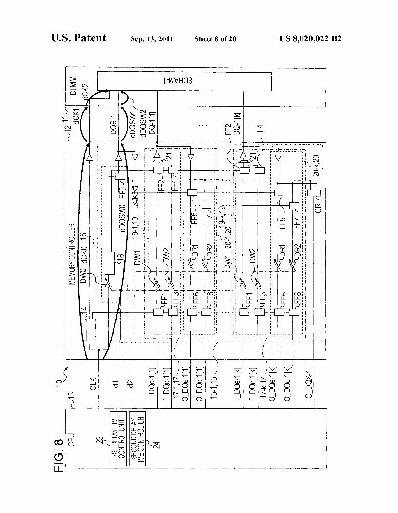
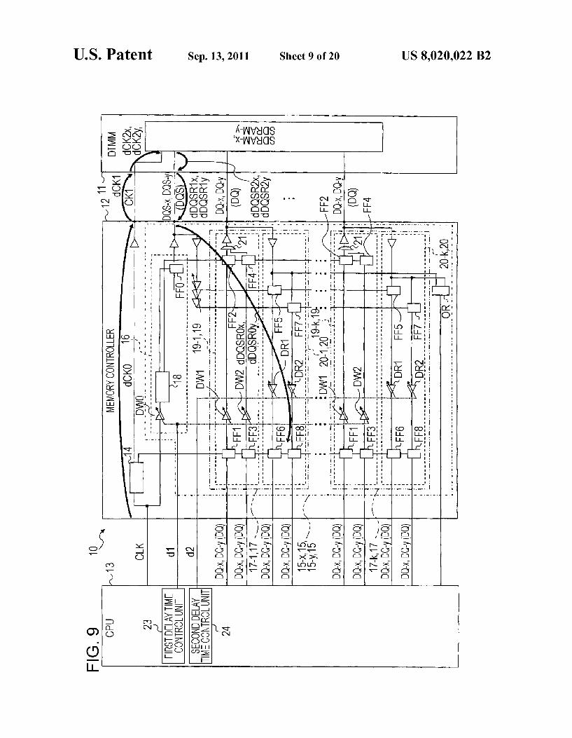
FIGS. 8 and 9 are each a block diagram for explaining calculation formulae used to determine the first delay time in the first delay time control unit of the information processing apparatus according to the first embodiment. At the time when the adjustment of the first delay times
Dt1-1 to Dt1-n is completed, the following formula (1) holds:
As shown in FIG.8, dCK0 represents a time from the input of the clock signal CLK to the memory controller 12 to the output of the clock signal CK1 from the memory controller 12, and dCK1 represents a time from the output of the clock signal CK1 from the memory controller 12 to the input thereof to the DIMM 11. Also, dCK2 represents a time from the input of the clock signal CK1 to the DIMM 11 to the input thereof to each of the SDRAM-1 to the SDRAM-n. In FIG. 8, dCK2 represents the time from the input of the clock signal CK1 to the DIMM 11 to the input thereof to the SDRAM-1.
Further, dDQSW0 represents a time from the input of the clock signal CLK to the memory controller 12 to the output of each of the data strobe signals DQS-1 to DQS-n from the memory controller 12. In FIG. 8, dDQSWO represents the time from the input of the clock signal CLK to the memory controller 12 to the output of the data strobe signal DQS-1 from the memory controller 12.
Also, dDQSW1 represents a time from the output of each of the data strobe signals DQS-1 to DQS-n from the memory controller 12 to the input thereof to the DIMM 11. In FIG. 8, dDQSW1 represents the time from the output of the data strobe signal DQS-1 from the memory controller 12 to the input thereof to the DIMM 11.
In addition, dDQSW2 represents a time from the input of each of the data strobesignals DQS-1 to DQS-nto the DIMM 11 to the input thereofto corresponding one of the SDRAM-1 to the SDRAM-n. In FIG. 8, dDQSW2 represents the time from the input of the data strobe signal DQS-1 to the DIMM 11 to the input thereof to the SDRAM-1.
Because the wirings for connection between the memory controller 12 and the DIMM11 are formed in the same length, dCK1=dDQSW1 holds in the formula (1) and hence the for mula (1) can be modified to the following formulae (2-1) and (2-2):
dCKO+dCK2=dDOSWO+dDOSW2 (2-1)
dCK2=dDOSWO-dCKO+dDOSW2 (2-2)
Assuming (dDQSW0-dCK0) to be a delay time Delay (W)n at the write operation in the n-channel SDRAM-n, the formula (2-2) can be rewritten into the following formula (2-3):
dCK2=Delay (W)n+dDOSW2 (2-3)
Thus, the first delay times Dt1-1 to Dt1-n corresponding respectively to the SDRAM-1 to the SDRAM-n are set so as to become longer gradually in the order from the 1-channel SDRAM-1 toward the n-channel SDRAM-n.
Further, the first delay time control unit 23 outputs the respective first control signals d1 to the first variable delay circuits DW-1 to DW-n so that the set first delay times Dt1-1 to Dt1-n are obtained. In accordance with the first control signals d1, the first variable delay circuits DW-1 to DW-n delay the data strobe signals DQS-1 to DQS-n by the first delay times Dt1-1 to Dt1-n, respectively. As described above, during the write operation, the first
variable delay circuit DW delays the data strobe signal DQS
US 8,020,022 B2 15
output to the SDRAM by the first delay time Dt1 that has been set based on the write leveling function. The second delay time control unit 24 controls the second
variable delay circuit DR, which is included in each of the control circuit units 15-1 to 15-in, to delay the data signal by the second delay time Dt2 in accordance with corresponding one of the first delay times Dt1-1 to Dt1-n set by the first delay time control unit 23, and it outputs the second control signal d2 for setting the second delay time Dt2. Further, in this embodiment, based on the first delay times Dt1-1 to Dt1-n set by the first delay time control unit 23, the second delay time control unit 24 calculates and sets the respective second delay times Dt2 for the data signals DQ-1 to DQ-n that are input respectively from the plural SDRAMs of SDRAM-1 to SDRAM-n in the read operation. More specifically, the second delay time control unit 24
sets respective delay times Delay(R) for the data signals DQ-1 to DQ-n that are input respectively from the SDRAM-1 to the SDRAM-n. As shown in FIG. 9, for example, for an x-channel (x is a natural number) SDRAM-X and a y-channel (y is a natural number) SDRAM-y, the following formulae (3-1) and (3-2) hold regarding respective lapsed times Pass (R)x and Pass(R)y from the input of the clock signal CLK to the memory controller 12 to the output of the data signals DQ-X and DQ-y to the CPU 13 from the memory controller 12:
dDOSR13+dDOSROx (3-1)
As shown in FIG. 9, similarly to the case of FIG. 8, dCK0 represents a time from the input of the clock signal CLK to the memory controller 12 to the output of the clock signal CK1 from the memory controller 12, and dCK1 represents a time from the output of the clock signal CK1 from the memory controller 12 to the input thereofto the DIMM 11. In addition, dCK2x represents a time from the input of the clock signal CK1 to the DIMM 11 to the input thereof to the x-channel SDRAM-X, and dDQSR2x represents a time from the output of an x-channel data strobe signal DQS-X from the x-channel SDRAM-x to the output thereoffrom the DIMM 11. Further, dDQSR1.x represents a time from the output of the x-channel data strobe signal DQS-X from the DIMM 11 to the input thereof to the memory controller 12, and dDQSR0x repre sents a time from the input of the X-channel data strobe signal DQS-X to the memory controller 12 to the input of the data signal DQ-X to the flip-flop FF6 or the flip-flop FF8.
Moreover, as shown in FIG. 9, dCK2y represents a time from the input of the clock signal CK1 to the DIMM 11 to the input thereof to the y-channel SDRAM-y, and dDQSR2y represents a time from the output of a y-channel data strobe signal DQS-y from the y-channel SDRAM-y to the output thereof from the DIMM 11. Further, dDQSR1y represents a time from the output of the y-channel data strobe signal DQS-y from the DIMM 11 to the input thereof to the memory controller 12, and dDQSR0y represents a time from the input of the y-channel data strobe signal DQS-y to the memory controller 12 to the input of the data signal DQ-y to the flip-flop FF6 or the flip-flop FF8.
Herein, in order to make the lapsed time Pass(R)x in the X-channel and the lapsed time Pass(R)y in they-channel equal to each other, the following formula (3-3) has to be satisfied:
(3-2)
dDOSR1y--dDOSROy (3-3)
10
15
25
30
35
40
45
50
55
60
65
16 Because the wirings for connection between the memory
controller 12 and the DIMM11 are formed in the same length, dDQSR2x=dDQSR2y and dDQSR1x-dDQSR1y hold in the formula (3-3) and hence the formula (3-3) can be modified to the following formula (3-4):
Assuming herein dDQSR0x=Delay (R)x--C. and dDQSW2x-dDQSW2y and substituting those relations in the above-mentioned formula (2-3), the following formula (3-5) is obtained:
(3-4)
Delay(Wx+Delay (R)x=Delay (Wy+Delay (R)y
The formula (3-5) can be generalized into the following formula (3-6):
(3-5)
Delay (R)n=max(Delay(W))-Delay (W)n (3-6)
The delay time thus calculated is provided as Delay (R)n. In other words, the second delay time Dt2 for the data signal DQ input from the SDRAM can be calculated by using the first delay time Dt1 that has been set in the write leveling.
Accordingly, in the second delay time control unit 24, the second delay time Dt2-x corresponding to one SDRAM-x is set by using the above-mentioned formula (3-5) so that the sum of the first delay time Dt1-x and the second delay time Dt2-x both corresponding to the relevant SDRAM-x is equal to a preset value.
Also, in the second delay time control unit 24, the second delay time Dt2-x corresponding to one SDRAM-x is set by using the above-mentioned formula (3-5) so that the sum of the first delay time Dt1-x and the second delay time Dt2-y both corresponding to the relevant SDRAM-x is equal to the sum of the first delay time Dt1-y and the second delay time Dt2-y both corresponding to another SDRAM-y.
Further, in the second delay time control unit 24, the sec ond delay time Dt2-x corresponding to one SDRAM-x is set by using the above-mentioned formula (3-6) to be the differ ence between the first delay time Dt1-x corresponding to the relevant SDRAM-X and a maximum delay time Dt1-n among the plurality of first delay times Dt1-1 to Dt1-n corresponding respectively to the SDRAM-1 to the SDRAM-n.
Thus, the second delay times Dt2-1 to Dt2-n corresponding respectively to the SDRAM-1 to the SDRAM-n are set so as to become shorter gradually in the order from the 1-channel SDRAM-1 toward the n-channel SDRAM-n.
Further, the second delay time control unit 24 outputs the respective second control signals d2 to the second variable delay circuits DR-1 to DR-n so that the set second delay times Dt2-1 to Dt2-n are obtained. In accordance with the second control signals d2, the second variable delay circuits DR-1 to DR-n delay the data signals DQ-1 to DQ-n by the second delay times Dt2-1 to Dt2-n, respectively.
In other words, during the read operation, the second vari able delay circuit DR delays the data signal DQ input from the SDRAM by the second delay time Dt2 that has been set based on the first delay time Dt1. An example of the write operation executed using the first
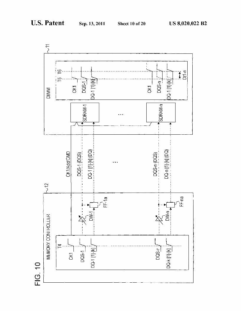
variable delay circuit DW in the above-described information processing apparatus 10 according to the first embodiment will be described below with reference to FIG. 10.
For the sake of convenience, the following description is made in connection with the case where the write operation is executed on the 1-channel SDRAM-1 and the n-channel SDRAM-n.
Also, for the sake of convenience, in the following descrip tion, the flip-flops FF2 and FF4 corresponding to the 1-chan
US 8,020,022 B2 17
nel SDRAM-1 are each denoted by FF-1a, and the flip-flops FF2 and FF4 corresponding to the n-channel SDRAM-n are each denoted by FF-na. The first delay time control unit 23 sets the first delay times
Dt1-1 to Dt1-n, which correspond respectively to the SDRAM-1 to the SDRAM-n, based on the write leveling function, and then outputs the respective first control signals d1, which correspond to the set first delay times Dt1-1 to Dt1-n, to the corresponding first variable delay circuits DW-1 to DW-n (first delay time control step).
After the first delay times Dt1-1 to Dt1-n have been set respectively in the first variable delay circuits DW-1 to DW-n, the write operation is executed as follows.
The memory controller 12 outputs the clock signal CK1 to each SDRAM (SDRAM-1 and SDRAM-n in the example of FIG. 10), and it also generates each data strobe signal (DQS-1 and DQS-n in the example of FIG. 10) substantially at the same time as the output of the clock signal CK1 and then outputs the generated data strobe signal to each first variable delay circuit (DW-1 and DW-ninthe example of FIG.10) (see a time “T4” in FIG. 10).
In the case shown in FIG. 10, the first variable delay circuit DW-1 outputs the input data strobe signal DQS-1 to the SDRAM-1 and the flip-flop FF-1a without delaying it, while the first variable delay circuit DW-n outputs the input data strobesignal DQS-n to the SDRAM-nand the flip-flop FF-na after delaying it by the delay time Dt1-n.
Further, the memory controller 12 outputs the data signals DQ-11 to -k, which correspond to the SDRAM-1, to the flip-flop FF-1a through respective first variable delay circuits (not shown, each of which has the same construction as the first variable delay circuit DW-1) substantially at the same time as the data strobesignal DQS-1, and also outputs the data signals DQ-n1 to -k, which correspond to the SDRAM-n, to the flip-flop FF-na through respective first variable delay circuits (not shown, each of which has the same construction as the first variable delay circuit DW-n) substantially at the same time as the data strobe signal DQS-n. When the data strobe signal DQS-1 is input, the flip-flop
FF-1a outputs the data signals DQ-11 to k to the SDRAM 1. Similarly, when the data strobe signal DQS-n is input, the flip-flop FF-na outputs the data signals DQ-n1 to k to the SDRAM-n. The data strobe signal DQS-1 and the data signals DQ-11
to k are input to the SDRAM-1 substantially at the same time as the clock signal CK1 (see a time “T5” in FIG.10). The data strobe signal DQS-n and the data signals DQ-n1 to k are input (see a time “T6” in FIG. 10) to the SDRAM-n substantially at the same time as the clock signal CK1 which has been delayed by the first delay time Dt1-n after the input of the clock signal CK1 to the SDRAM-1 (see the time “T5” in FIG. 10). As a result, the data strobe signal DQS and the data signals
DQ are input to each of the SDRAM-1 to the SDRAM-n Substantially at the same time as the clock signal CK1, whereby the write operation is executed. An example of the read operation executed using the sec
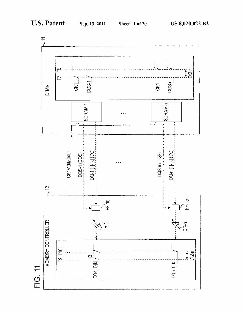
ond variable delay circuit DR in the above-described infor mation processing apparatus 10 according to the first embodi ment will be described below with reference to FIG. 11.
For the sake of convenience, the following description is made in connection with the case where the read operation is executed on the 1-channel SDRAM-1 and the n-channel SDRAM-n.
Also, for the sake of convenience, in the following descrip tion, the flip-flops FF5 and FFT corresponding to the 1-chan
10
15
25
30
35
40
45
50
55
60
65
18 nel SDRAM-1 are each denoted by FF-1b, and the flip-flops FF5 and FF7 corresponding to the n-channel SDRAM-n are each denoted by FF-nb. The second delay time control unit 24 sets the second delay
times Dt2-1 to Dt2-n, which correspond respectively to the SDRAM-1 to the SDRAM-n, based on the first delay times Dt1-1 to Dt1-n corresponding respectively to the SDRAM-1 to the SDRAM-n, and then outputs the respective second control signals d2, which correspond to the set second delay times Dt2-1 to Dt2-n, to the corresponding second variable delay circuits DR-1 to DR-n (second delay time control step).
After the second delay times Dt2-1 to Dt2-n have been set respectively in the second variable delay circuits DR-1 to Dr-n, the read operation is executed as follows. The memory controller 12 outputs the clock signal CK1 to
each SDRAM (SDRAM-1 and SDRAM-n in the example of FIG. 11) (see a time “T7 in FIG. 11). In this embodiment, since the clock signal line is wired to the SDRAM-1 to the SDRAM-n through the daisy chain connection, the clock signal CK1 is successively input to the SDRAM-1 to the SDRAM-n one after another.
Therefore, the clock signal CK1 is input to the SDRAM-n with a delay of the second delay time Dt2-n after the input of the clock signal CK1 to the SDRAM-1 (see a time “T8” in FIG. 11).
In the case shown in FIG. 11, when the clock signal CK1 is input, the SDRAM-1 outputs the data strobe signal DQS-1 and the data signals DQ-11 to -k to the flip-flop FF-1 b in the memory controller 12 (see the time “T7 in FIG. 11). Similarly, when the clock signal CK1 is input with the delay of the second delay time Dt2-n after the input of the clock signal CK1 to the SDRAM-1, the SDRAM-n outputs the data strobe signal DQS-n and the data signals DQ-n1 to -k to the flip-flop FF-nb in the memory controller 12 (see the time “T8” in FIG. 11). When the data strobe signal DQS-1 is input, the flip-flop
FF-1b outputs the data signals DQ-11 to -k to the second variable delay circuit DR-1. Similarly, when the data strobe signal DQS-n is input, the flip-flop FF-nb outputs the data signals DQ-n1 to -k to the second variable delay circuit DR-n. The second variable delay circuit DR-n outputs the input
the data signals DQ-n1 to -k to the CPU 13 (not shown in FIG. 11) without delaying them, while the second variable delay circuit DR-1 outputs the input the data signals DQ-11 to -k to the CPU 13 after delaying them by the second delay time Dt2-n (see a time “T9”, a time “T10 and a dotted line “B” in FIG. 11). As a result, the respective data signals DQ corresponding to
the SDRAM-1 to the SDRAM-n are input to the CPU 13 substantially at the same time, whereby the read operation is executed.
Thus, with the information processing apparatus 10 according to the first embodiment, for the plurality of SDRAMS of SDRAM-1 to SDRAM-n to which the clock signal line is wired through the daisy chain connection, the input times of the respective data signals DQ output from the SDRAM-1 to the SDRAM-n, to which the clock signal line is wired through the daisy chain connection, can be easily matched with one another by setting, based on the first delay time Dt1 set by utilizing the write leveling function, the second delay time Dt2 for each data signal DQ input from the SDRAM in the read operation. Accordingly, a failure due to a delay in propagation of the data signal DQ can be prevented in control of the read operation.
Also, with the provision of the second variable delay circuit DR for delaying the data signal by the second delay time Dt2
US 8,020,022 B2 19
based on the first delay time Dt1 that has been set by utilizing the write leveling function, a memory interface capable of matching the input times of the respective data signals DQ output from the SDRAM-1 to the SDRAM-n with one another, to which the clock signal line is wired through the daisy chain connection, can be simply realized without pro viding a special mechanism, such as an FIFO.
Further, since the plural data signal lines connecting the memory controller 12 and the DIMM 11 to each other are formed in the same length, the formula for calculating the second delay time Dt2 is simplified and the second delay time Dt2 for the data signal DQ input from the SDRAM during the read operation can be easily obtained.
Moreover, since the sum of the first delay time Dt1 and the second delay time Dt2 both corresponding to one SDRAM is set equal to the preset value and the sum of the first delay time Dt1 and the second delay time Dt2 both corresponding to one SDRAM is set equal to the sum of the first delay time Dt1 and the second delay time Dt2 both corresponding to another SDRAM, criteria for setting the second delay time Dt2 can be clarified based on the first delay time Dt1 that has been set by utilizing the write leveling function, and the respective sec ond delay times Dt2 for the plurality of SDRAMs can be easily determined.
In addition, since the second delay time Dt2 corresponding to one SDRAM is set to be the difference between the first delay time Dt1 corresponding to the relevant SDRAM and a maximum delay time Dt1-n among the plurality of first delay times Dt1-1 to Dt1-n corresponding respectively to the SDRAM-1 to the SDRAM-n, the formula for calculating the second delay time Dt2 is generalized and the respective sec ond delay times Dt2 for the SDRAM-1 to the SDRAM-n can be more easily obtained.
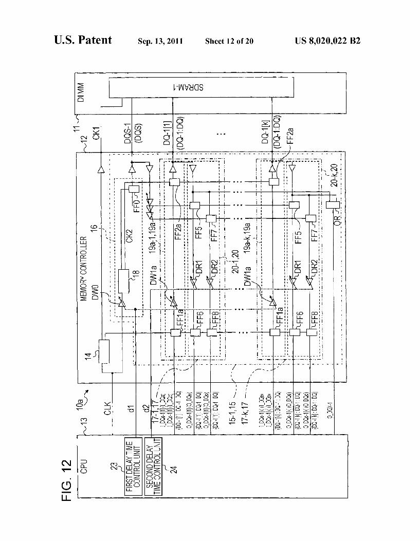
2 Modification of First Embodiment
A modification of the information processing apparatus 10 according to the first embodiment will be described below with reference to FIGS. 12 and 13.
FIG. 12 is a circuit diagram showing a portion of the memory controller, which corresponds to the SDRAM-1, in the information processing apparatus according to a modifi cation of the first embodiment, and FIG. 13 is a circuit dia gram showing a portion of the memory controller, which corresponds to the SDRAM-n, in the information processing apparatus according to the modification. As shown in FIGS. 12 and 13, an information processing
apparatus 10a according to the modification of the first embodiment includes DQ signal input control units 19a-1 to 19a-kinstead of the DQ signal input control units 19-1 to 19-k in each of the control circuit units 15-1 to 15-in in the first embodiment. The remaining part of the information process ing apparatus 10a is constructed similarly to that of the infor mation processing apparatus 10 according to the first embodi ment. Note that because the same characters in FIGS. 12 and 13
as the above-mentioned characters denote the same or essen tially the same components, a detailed description thereof is omitted here.
In the following description, regarding characters denoting the DQ signal input control units in the modification of the first embodiment, when one among the plurality of DQ signal input control units needs to be specified, any of characters 19a-1 to 19a-kis used, while just a character 19a is used when an arbitrary DQ signal input control unit is to be indicated. As with the above-described DQ signal input control units
19 in the first embodiment, the DQ signal input control unit
10
15
25
30
35
40
45
50
55
60
65
20 19a in the modification of the first embodiment executes control to output the first data signal I DQe and the second data signal I DQo, which are input from the CPU 13, to the SDRAM in the write operation. Unlike the above-described DQ signal input control unit 19 in the first embodiment, however, the DQ signal input control unit 19a executes the control Such that the first data signal I DQe and the second data signal I DQo are output to the SDRAM in a multiplied State.
Note that because a method for outputting the first data signal I DQe and the second data signal I DQo to the SDRAM in a multiplied state is a known technique, a detailed description of the method is omitted here. As shown in FIGS. 12 and 13, for example, the DQ signal
input control unit 19a in the modification of the first embodi ment comprises a flip-flop FF1a, a first variable delay circuit (first variable delay unit) DW1a, and a flip-flop FF2a. The flip-flop FF1a outputs the first data signal I DQe or the
second data signal I DQo, which is input from the CPU 13, to the first variable delay circuit DW1a when the clock signal CK1 generated from the first clock signal generator 14 is input. The first variable delay circuit DW1a is a digital delay
circuit for delaying the first data signal I DQe or the second data signal I DQo, which is input from the flip-flop FF1a, in accordance with the first control signal d1 from the first delay time control unit 23, and for outputting the delayed first or second data signal to the flip-flop FF2a. For example, the first variable delay circuit DW1a delays the first data signal I DQe or the second data signal I DQo, which is input from the flip-flop FF1a, by the first delay time Dt1-1 set by the first delay time control unit 23 and then outputs the delayed first or second data signal to the flip-flop FF2a. The flip-flop FF2a outputs the first data signal I DQe or the
second data signal I DQo, which is input from the first vari able delay circuit DW1a, to the SDRAM when the clock signal CK2 generated from the second clock signal generator 18 is input.
Thus, the information processing apparatus 10a according to the modification of the first embodiment can also provide similar working advantages to those in the first embodiment.
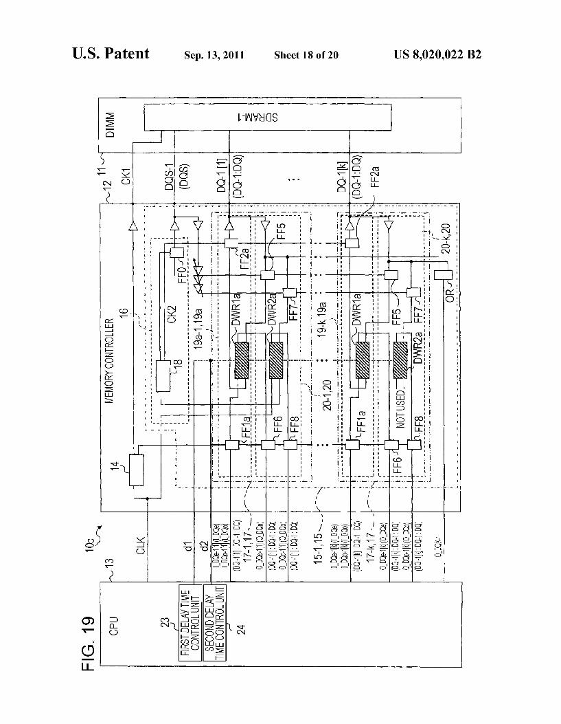
3 Second Embodiment
An information processing apparatus 10b according to a second embodiment will be described with reference to FIGS. 14 and 15.
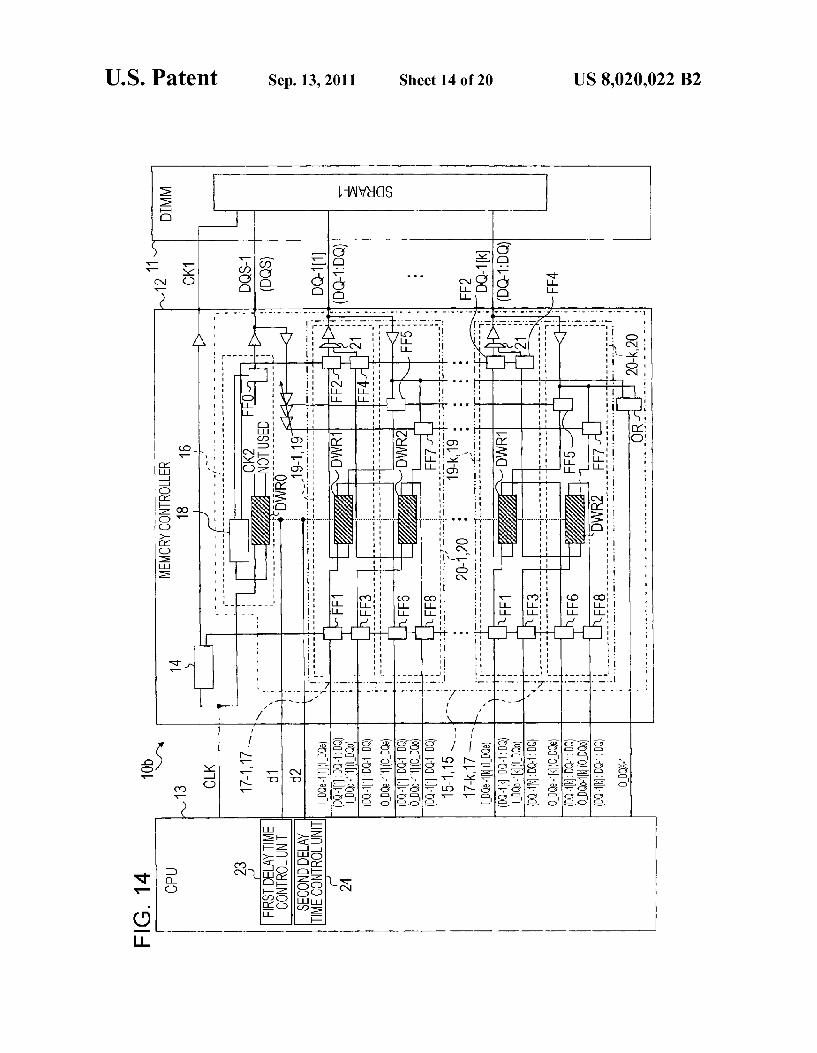
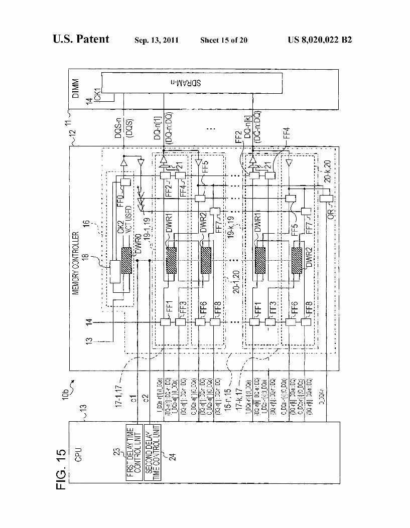
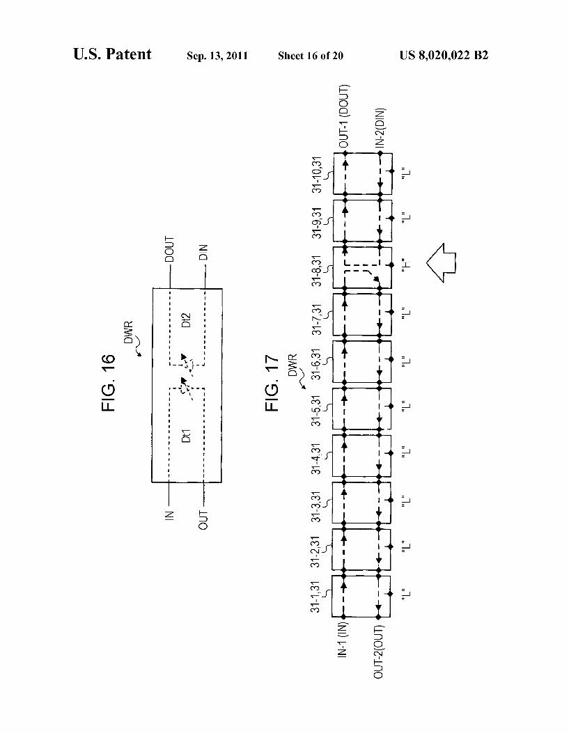
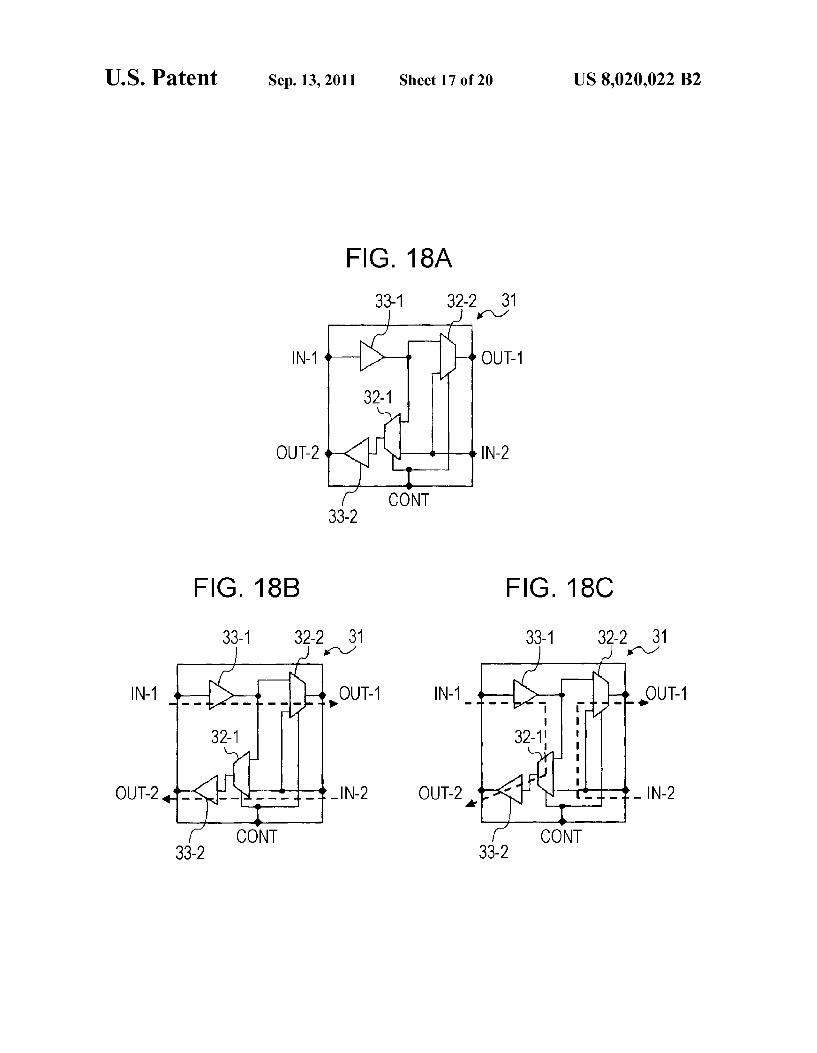
FIG. 14 is a circuit diagram showingaportion of a memory controller, which corresponds to the SDRAM-1, in the infor mation processing apparatus according to the second embodi ment, FIG. 15 is a circuit diagram showing a portion of the memory controller, which corresponds to SDRAM-n, in the information processing apparatus according to the second embodiment, and FIG. 16 is a diagram for explaining the function of a third variable delay circuit of the memory con troller. As shown in FIGS. 14 and 15, the information processing
apparatus 10b according to the second embodiment includes a third variable delay circuit DWR0 instead of the first vari able delay circuit DW0 included in each of the control circuit units 15-1 to 15-in in the first embodiment, a third variable delay circuit DWR1 instead of the first variable delay circuit DW1 and the second variable delay circuit DR1 both included in each of the control circuit units 15-1 to 15-in in the first embodiment, and a third variable delay circuit DWR2 instead of the first variable delay circuit DW2 and the second variable delay circuit DR2 both included in each of the control circuit
US 8,020,022 B2 21
units 15-1 to 15-in in the first embodiment. The remaining part of the information processing apparatus 10b is constructed similarly to that of the information processing apparatus 10 according to the first embodiment.
Note that because the same characters in FIGS. 14 to 16 as the above-mentioned characters denote the same or essen tially the same components, a detailed description thereof is omitted here.
In the following description, regarding characters denoting the third variable delay circuits in the second embodiment, when one among the plurality of third variable delay circuits needs to be specified, any of characters DWR0. DWR1 and DWR2 is used, while just a character DWR is used when an arbitrary third variable delay circuit is to be indicated. The third variable delay circuit DWR in the second
embodiment is a digital delay circuit capable of delaying two signals at the same time. As shown in FIG. 16, the third variable delay circuit DWR has two input terminals IN and DIN and two output terminals OUT and DOUT. A signal input through one input terminal IN is delayed by the first delay time Dt1 which is set by the first delay time control unit 23, and is output from one output terminal OUT, while a signal input through the other input terminal DIN is delayed by the second delay time Dt2 which is set by the second delay time control unit 24, and is output from the other output terminal DOUT.
In the example shown in FIGS. 14 and 15, in the third variable delay circuit DWR0, the clock signal CLK from the CPU 13 is input to one input terminal IN, is delayed by the first delay time Dt1, and is output to the second clock signal generator 18 from the one output terminal OUT. The other input terminal DIN and the other output terminal DOUT are not used.
Also, as shown in FIGS. 14 and 15, in the third variable delay circuit DWR1, the first data signal I DQe is input to one input terminal IN from the flip-flop FF1, is delayed by the first delay time Dt1, and is output to the flip-flop FF2 from the one output terminal OUT. The third data signal O DQe is input to the other input terminal DIN from the flip-flop FF5, is delayed by the second delay time Dt2, and is output to the flip-flop FF6 from the other output terminal DOUT.
Further, as shown in FIGS. 14 and 15, in the third variable delay circuit DWR2, the second data signal I DQo is input to one input terminal IN from the flip-flop FF3, is delayed by the first delay time Dt1, and is output to the flip-flop FF4 from the one output terminal OUT. The fourth data signal O DQo is input to the other input terminal DIN from the flip-flop FF7, is delayed by the second delay time Dt2, and is output to the flip-flop FF8 from the other output terminal DOUT.
FIG. 17 is a block diagram showing a configuration example of the third variable delay circuit in the information processing apparatus according to the second embodiment, and FIGS. 18A to 18C are circuit diagrams each showing a configuration example of a unit circuit of the third variable delay circuit. Specifically, FIG. 18A is a circuit diagram for explaining the configuration of the unit circuit, FIG. 18B is a circuit diagram for explaining a through operation mode of the unit circuit, and FIG. 18C is a circuit diagram for explain ing a feedback operation mode of the unit circuit. The detailed configuration of the third variable delay cir
cuit DWR will be described below with reference to FIGS. 17 and 18A to 18C. As shown in FIG. 17, the third variable delay circuit DWR
in the second embodiment is constituted by connecting a plurality (ten in the example shown in FIG. 17) of unit circuits 31-1 to 31-10 in Series.
10
15
25
30
35
40
45
50
55
60
65
22 In the following description, regarding characters denoting
the unit circuits, when one among the plurality of unit circuits needs to be specified, any of characters 31-1 to 31-10 is used, while just a character 31 is used when an arbitrary unit circuit is to be indicated. The unit circuit 31 is a circuit capable of selectively chang
ing the terminal from which the input signal is to be output. As shown in FIG. 18A, the unit circuit 31 comprises a control signal input terminal CONT, a first selector (selectively changing unit) 32-1, a second selector (selectively changing unit) 32-2, a first input terminal IN-1, a second input terminal IN-2, a first output terminal OUT-1, and a second output terminal OUT-2. The control signal input terminal CONT is a terminal to
which the control signal from the first delay time control unit 23 or the second delay time control unit 24 is input, and which is connected to both the first selector 32-1 and the second selector 32-2 (each being described below). The first selector 32-1 serves to selectively change an out
put signal in accordance with the control signal from the control signal input terminal CONT, and it has two input terminals and one output terminal. The second selector 32-2 serves to selectively change an
output signal in accordance with the control signal from the control signal input terminal CONT, and it has two input terminals and one output terminal. The first input terminal IN-1 is a terminal to which a first
signal is input. As shown in FIG. 18A, the first input terminal IN-1 is connected to one input terminal of the first selector 32-1 and one input terminal of the second selector 32-2 through an amplifier 33-1. The second input terminal IN-2 is a terminal to which a
second signal is input. As shown in FIG. 18A, the second input terminal IN-2 is connected to the other input terminal of the first selector 32-1 and the other input terminal of the second selector 32-2. The first output terminal OUT-1 is a terminal for selectively
outputting one of the first signal input to the first input termi nal IN-1 and the second signal input to the second input terminal IN-2. As shown in FIG. 18A, the first output terminal IN-2 is connected to an output terminal of the second selector 32-2. The second output terminal OUT-2 is a terminal for selec
tively outputting one of the first signal input to the first input terminal IN-1 and the second signal input to the second input terminal IN-2. As shown in FIG. 18A, an output terminal of the first selector 32-1 is connected to the second output ter minal OUT-2 through an amplifier 33-2.
Further, the unit circuit 31 is constructed to be capable of selectively operating in one of the through operation mode and the feedback operation mode in accordance with the control signal from the control signal input terminal CONT. The term “through operation mode” refers to a mode in
which, as shown in FIG. 18B, the first signal input through the first input terminal IN-1 is output through the first output terminal OUT-1 and the second signal input through the sec ond input terminal IN-2 is output through the second output terminal OUT-2. The term “feedback operation mode” refers a mode in
which, as shown in FIG. 18C, the first signal input through the first input terminal IN-1 is output through the second output terminal OUT-2 and the second signal input through the sec ond input terminal IN-2 is output through the first output terminal OUT-1.
Further, in the third variable delay circuit DWR, as shown in FIG. 17, the plurality of unit circuits 31-1 to 31-10 are connected in series, and the adjacent unit circuits 31 are
US 8,020,022 B2 23
connected to each other such that the first input terminal IN-1 is connected to the first output terminal OUT-1 and the second input terminal IN-2 is connected to the second output termi nal OUT-2.
Stated another way, in the through operation mode, the first signal input from the unit circuit 31 in the preceding stage is output to the unit circuit 31 in the Succeeding stage and the second signal input from the unit circuit 31 in the Succeeding stage is output to the unit circuit 31 in the preceding stage. In the feedback operation mode, the first signal input from the unit circuit 31 in the preceding stage is output to the unit circuit 31 in the preceding stage, and the second signal input from the unit circuit 31 in the Succeeding stage is output to the unit circuit 31 in the Succeeding stage.
Moreover, in the second embodiment, the first delay time control unit 23 executes control to delay the first signal by the first delay time Dt1 by causing the first signal to pass a part of the third variable delay circuit DWR, and the second delay time control unit 24 executes control to delay the second signal by the second delay time Dt2 by causing the second signal to pass a part of the third variable delay circuit DWR. More specifically, each of the first delay time control unit
23 and the second delay time control unit 24 outputs control signals to the plurality of unit circuits 31-1 to 31-10 for operating one of the unit circuits 31-1 to 31-10 in the feedback operation mode and operating the other unit circuits in the through operation mode based on the first delay time Dt1 and the second delay time Dt2 corresponding to the first delay time Dt1, which are set by the first delay time control unit 23 and the second delay time control unit 24, respectively.
In accordance with the control signals output to the unit circuits 31-1 to 31-10 from each of the first delay time control unit 23 and the second delay time control unit 24, the third variable delay circuit DWR increases and decreases the num ber of the unit circuits 31 through which the first signal input to the first input terminal IN-1 of the unit circuit 31-1 in the foremost stage or the second signal input to the second input terminal IN-2 of the unit circuit 31-1 in the rearmost stage passes, thereby changing the delay time from the input of the first signal or the second signal to the output thereof.
For example, as shown in FIG. 17, based on the first delay time Dt1 and the second delay time Dt2 which are set by the first delay time control unit 23 and the second delay time control unit 24, respectively, a “Hi' signal is output to the unit circuit 31-8 and a “Low” signal is output to the unit circuits 31-1 to 31-7, 31-9 and 31-10 other than the unit circuit 31-8. In such a case, the third variable delay circuit DWR forms a first signal passage line and a second signal passage line by operating the unit circuit 31-8 in the feedback operation mode and operating the unit circuits 31-1 to 31-7, 31-9 and 31-10 in the through operation mode.
In the first signal passage line, as shown in FIG. 17, the first signal input through the first input terminal IN-1 of the unit circuit 31-1 in the foremost stage Successively passes the plurality of unit circuits 31-2 to 31-7, which operate in the through operation mode, from the unit circuit 31-2 to the unit circuit 31-7. After being returned at the unit circuit 31-8 which operates in the feedback operation mode, the first signal Successively passes the plurality of unit circuits 31-2 to 31-7, which operate in the through operation mode, from the unit circuit 31-7 to the unit circuit 31-2. Finally, the first signal is output from the second output terminal OUT-2 of the unit circuit 31-1 in the foremost stage.
In the second signal passage line, as shown in FIG. 17, the second signal input through the second input terminal IN-2 of the unit circuit 31-10 in the rearmost stage passes the unit circuit 31-9 which operates in the through operation mode.
10
15
25
30
35
40
45
50
55
60
65
24 After being returned at the unit circuit 31-8 which operates in the feedback operation mode, the second signal passes the unit circuit 31-9 which operates in the through operation mode. Then, the second signal is output from the first output terminal OUT-1 of the unit circuit 31-10 in the rearmost stage. As a result, the third variable delay circuit DWR disposed
corresponding to each of the SDRAM-1 to the SDRAM-n executes the control such that the sum of the first delay time Dt1 and the second delay time Dt2 is kept constant.
Thus, the information processing apparatus 10b according to the second embodiment can provide the following advan tages in addition to similar working advantages to those of the above-described first embodiment. By using the unit circuits 31 constituted to be capable of selectively operating in the through operation mode in which the signal input from the unit circuit 31 in the preceding stage is output to the unit circuit 31 in the Succeeding stage and the signal input from the unit circuit 31 in the Succeeding stage is output to the unit circuit 31 in the preceding stage and in the feedback operation mode in which the signal input from the unit circuit 31 in the preceding stage is output to the unit circuit 31 in the preceding stage and the signal input from the unit circuit 31 in the Succeeding stage is output to the unit circuit 31 in the Suc ceeding stage, those two signals can be simultaneously delayed by the respective delay times Dt1 and Dt2 from the input of the two signals to the output thereof. Accordingly, the delay times Dt1 and Dt2 from the input of the two signals to the output thereof can be efficiently set without increasing the power consumption and the area occupied by the apparatus.
Also, by operating at least one unit circuit 31 among the plurality of unit circuits 31-1 to 31-10 in the feedback opera tion mode, the respective delay times Dt1 and Dt2 of the two signals can be easily set while holding constant the Sum of the respective delay times Dt1 and Dt2 of the two signals.
Further, by executing the control such that the sum of the first delay time Dt1 of the first signal and the second delay time Dt2 of the second signal is equal to a preset value, or Such that the sum of the first delay time Dt1 of the first signal and the second delay time Dt2 of the second signal is held con stant, the respective delay times Dt1 and Dt2 of the two signals can be easily set while holding constant the Sum of the respective delay times Dt1 and Dt2 of the two signals.
4) Modification of Second Embodiment
A modification of the information processing apparatus 10b according to the second embodiment will be described below with reference to FIGS. 19 and 20.
FIG. 19 is a circuit diagram showing a portion of the memory controller, which corresponds to the SDRAM-1, in the information processing apparatus according to a modifi cation of the second embodiment, and FIG. 20 is a circuit diagram showing a portion of the memory controller, which corresponds to the SDRAM-n, in the information processing apparatus according to the modification. As shown in FIGS. 19 and 20, an information processing
apparatus 10c according to the modification of the second embodiment includes, as in the modification of the first embodiment, DQ signal input control units 19a-1 to 19a-k instead of the DQ signal input control units 19-1 to 19-k in each of the control circuit units 15-1 to 15-in in the second embodiment. Correspondingly, the information processing apparatus 10c includes third variable delay circuits. DWR1a and DWR2a instead of the third variable delay circuits DWR0, DWR1 and DWR2 in each of the control circuit units 15-1 to 15-in in the second embodiment. The remaining part of the information processing apparatus 10C is constructed simi
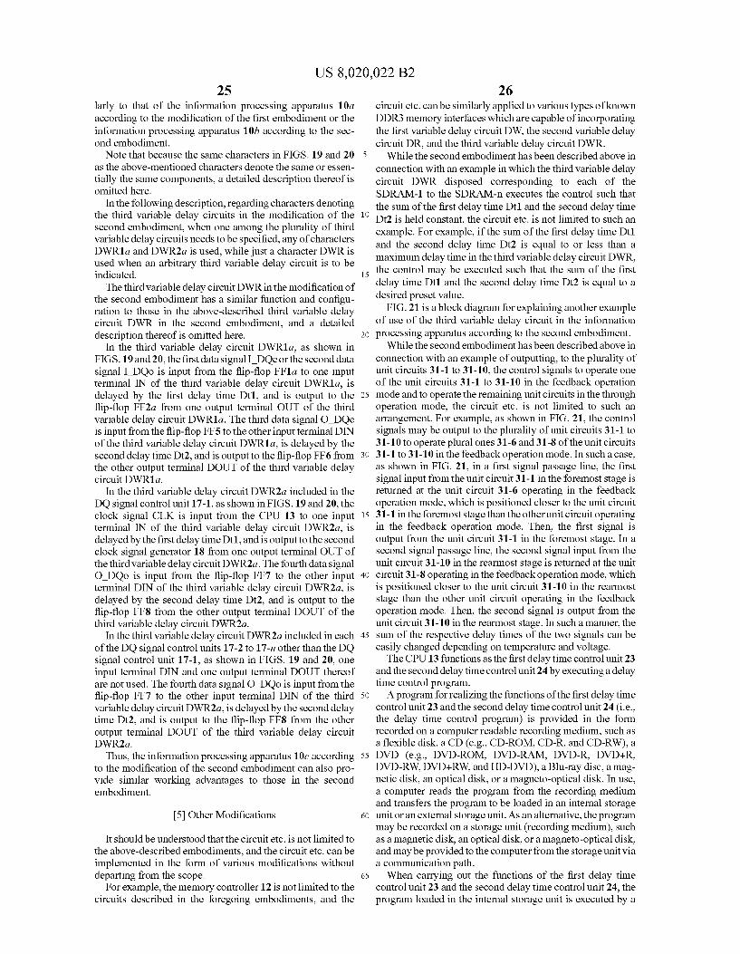
US 8,020,022 B2 25
larly to that of the information processing apparatus 10a according to the modification of the first embodiment or the information processing apparatus 10b according to the sec ond embodiment.
Note that because the same characters in FIGS. 19 and 20 as the above-mentioned characters denote the same or essen tially the same components, a detailed description thereof is omitted here.
In the following description, regarding characters denoting the third variable delay circuits in the modification of the second embodiment, when one among the plurality of third variable delay circuits needs to be specified, any of characters DWR1a and DWR2a is used, while just a character DWR is used when an arbitrary third variable delay circuit is to be indicated. The third variable delay circuit DWR in the modification of
the second embodiment has a similar function and configu ration to those in the above-described third variable delay circuit DWR in the second embodiment, and a detailed description thereof is omitted here.
In the third variable delay circuit DWR1a, as shown in FIGS. 19 and 20, the first data signal I DQe or the second data signal I DQo is input from the flip-flop FF1a to one input terminal IN of the third variable delay circuit DWR1a, is delayed by the first delay time Dt1, and is output to the flip-flop FF2a from one output terminal OUT of the third variable delay circuit DWR1a. The third data signal O DQe is input from the flip-flop FF5 to the other input terminal DIN of the third variable delay circuit DWR1a, is delayed by the second delay time Dt2, and is output to the flip-flop FF6 from the other output terminal DOUT of the third variable delay circuit DWR1a.
In the third variable delay circuit DWR2a included in the DQ signal control unit 17-1, as shown in FIGS. 19 and 20, the clock signal CLK is input from the CPU 13 to one input terminal IN of the third variable delay circuit DWR2a, is delayed by the first delay time Dt1, and is output to the second clock signal generator 18 from one output terminal OUT of the third variable delay circuit DWR2a. The fourth data signal O DQo is input from the flip-flop FF7 to the other input terminal DIN of the third variable delay circuit DWR2a, is delayed by the second delay time Dt2, and is output to the flip-flop FF8 from the other output terminal DOUT of the third variable delay circuit DWR2a.
In the third variable delay circuit DWR2a included in each of the DQ signal control units 17-2 to 17-nother than the DQ signal control unit 17-1, as shown in FIGS. 19 and 20, one input terminal DIN and one output terminal DOUT thereof are not used. The fourth data signal O DQo is input from the flip-flop FF7 to the other input terminal DIN of the third variable delay circuit DWR2a, is delayed by the second delay time Dt2, and is output to the flip-flop FF8 from the other output terminal DOUT of the third variable delay circuit DWR2.
Thus, the information processing apparatus 10c according to the modification of the second embodiment can also pro vide similar working advantages to those in the second embodiment.
5. Other Modifications
It should be understood that the circuit etc. is not limited to the above-described embodiments, and the circuit etc. can be implemented in the form of various modifications without departing from the scope.
For example, the memory controller 12 is not limited to the circuits described in the foregoing embodiments, and the
10
15
25
30
35
40
45
50
55
60
65
26 circuit etc. can be similarly applied to various types of known DDR3 memory interfaces which are capable of incorporating the first variable delay circuit DW, the second variable delay circuit DR, and the third variable delay circuit DWR.
While the second embodiment has been described above in connection with an example in which the third variable delay circuit DWR disposed corresponding to each of the SDRAM-1 to the SDRAM-n executes the control Such that the sum of the first delay time Dt1 and the second delay time Dt2 is held constant, the circuit etc. is not limited to such an example. For example, if the sum of the first delay time Dt1 and the second delay time Dt2 is equal to or less than a maximum delay time in the third variable delay circuit DWR, the control may be executed such that the sum of the first delay time Dt1 and the second delay time Dt2 is equal to a desired preset value.
FIG. 21 is a block diagram for explaining another example of use of the third variable delay circuit in the information processing apparatus according to the second embodiment.
While the second embodiment has been described above in connection with an example of outputting, to the plurality of unit circuits 31-1 to 31-10, the control signals to operate one of the unit circuits 31-1 to 31-10 in the feedback operation mode and to operate the remaining unit circuits in the through operation mode, the circuit etc. is not limited to such an arrangement. For example, as shown in FIG. 21, the control signals may be output to the plurality of unit circuits 31-1 to 31-10 to operate plural ones 31-6 and 31-8 of the unit circuits 31-1 to 31-10 in the feedback operation mode. In such a case, as shown in FIG. 21, in a first signal passage line, the first signal input from the unit circuit 31-1 in the foremost stage is returned at the unit circuit 31-6 operating in the feedback operation mode, which is positioned closer to the unit circuit 31-1 in the foremost stage than the other unit circuit operating in the feedback operation mode. Then, the first signal is output from the unit circuit 31-1 in the foremost stage. In a second signal passage line, the second signal input from the unit circuit 31-10 in the rearmost stage is returned at the unit circuit 31-8 operating in the feedback operation mode, which is positioned closer to the unit circuit 31-10 in the rearmost stage than the other unit circuit operating in the feedback operation mode. Then, the second signal is output from the unit circuit 31-10 in the rearmost stage. In Such a manner, the Sum of the respective delay times of the two signals can be easily changed depending on temperature and Voltage. The CPU 13 functions as the first delay time control unit 23
and the second delay time control unit 24 by executing a delay time control program. A program for realizing the functions of the first delay time
control unit 23 and the second delay time control unit 24 (i.e., the delay time control program) is provided in the form recorded on a computer readable recording medium, Such as a flexible disk, a CD (e.g., CD-ROM, CD-R, and CD-RW), a DVD (e.g., DVD-ROM, DVD-RAM, DVD-R, DVD+R, DVD-RW, DVD+RW, and HD-DVD), a Blu-ray disc, a mag netic disk, an optical disk, or a magneto-optical disk. In use, a computer reads the program from the recording medium and transfers the program to be loaded in an internal storage unit or an external storage unit. As an alternative, the program may be recorded on a storage unit (recording medium). Such as a magnetic disk, an optical disk, or a magneto-optical disk, and may be provided to the computer from the storage unit via a communication path. When carrying out the functions of the first delay time
control unit 23 and the second delay time control unit 24, the program loaded in the internal storage unit is executed by a
US 8,020,022 B2 27
microprocessor in the computer. As an alternative, the com puter may read and execute the program recorded on the recording medium.
In the embodiments, the term “computer represents the concept including hardware and an operating system, and it refers to hardware operating under control of the operating system. Also, when hardware is operated by an application program alone without using the operating system, the hard ware itself corresponds to the computer. The hardware com prises at least a microprocessor, such as a CPU, and a means for reading a computer program recorded on a recording medium. In the embodiments, each of the information pro cessing apparatuses 10, 10a, 10b and 10c has the function of the computer.
The recording medium used in the embodiments is not limited to the above-described examples including a flexible disk, a CD, a DVD, a Blu-ray disc, a magnetic disk, an optical disk, and a magneto-optical disk. In addition, other various types of computer-readable media are also usable which include an IC card, a ROM cartridge, a magnetic tape, a punched card, an internal storage unit (e.g., a memory such as RAM or ROM) of a computer, an external storage unit, and a print on which a code. Such as a barcode, is printed.
Thus, the embodiments can be implemented in computing hardware and/or software. Such as (in a non-limiting example) any computing circuitry, computer that can store, retrieve, process and/or output data and/or communicate with other computers. The results produced can be displayed on a display of the computing hardware. A program/software implementing the embodiments may be recorded on com puter-readable media comprising computer-readable record ing media. The program/software implementing the embodi ments may also be transmitted over transmission communication media. An example of transmission commu nication media includes a carrier-wave signal.
Further, according to an aspect of the embodiments of the invention, any combinations of the described features, func tions, operations, and/or benefits can be provided.
The many features and advantages of the embodiments are apparent from the detailed specification and, thus, it is intended by the appended claims to cover all such features and advantages of the embodiments that fall within the true spirit and scope thereof. Further, since numerous modifica tions and changes will readily occur to those skilled in the art, it is not desired to limit the inventive embodiments to the exact construction and operation illustrated and described, and accordingly all Suitable modifications and equivalents may be resorted to, falling within the scope thereof. What is claimed is: 1. A memory control circuit having a write leveling func
tion and controlling read/write operations by Supplying a clock signal to a plurality of memories through a clock signal line which is wired to the plurality of memories through daisy chain connection, the memory control circuit comprising:
for each of the plurality of memories: a first variable delay unit delaying, in a write operation,
a data strobe signal output to the memory by a first delay time that is set by utilizing the write leveling function; and
a second variable delay unit delaying, in a read opera tion, a data signal input from the memory by a second delay time that is set based on the first delay time,
wherein the first variable delay unit is constituted by a digital
delay circuit which is made up of a plurality of unit circuits connected in series and which delays the data signal output to the memory by the first delay time by
10
15
25
30
35
40
45
50
55
60
65
28 passing the data signal through a predetermined num ber of the unit circuits; and
the second variable delay unit is constituted by the digi tal delay circuit which is made up of the plurality of unit circuits connected in series and which delays the data signal input from the memory by the second delay time by passing the data signal through a pre determined number of the unit circuits.
2. The memory control circuit according to claim 1, wherein a plurality of data signal lines connecting the memory control circuit and the plurality of memories are formed in same length.
3. The memory control circuit according to claim 2, wherein the second delay time corresponding to one of the memories is set Such that a sum of the first delay time and the second delay time both corresponding to the one memory is equal to a preset value.
4. The memory control circuit according to claim 2, wherein the second delay time corresponding to one of the memories is set Such that a sum of the first delay time and the second delay time both corresponding to the one memory is equal to a sum of the first delay time and the second delay time both corresponding to another one of the memories.
5. The memory control circuit according to claim 2, wherein the second delay time corresponding to one of the memories is set to be a difference between the first delay time corresponding to the one memory and a maximum delay time from among the plurality of first delay times corresponding to the plurality of memories.
6. The memory control circuit according to claim 1, wherein the first variable delay unit and the second variable delay unit are each constituted by a digital delay circuit.
7. A delay time control device setting a signal delay time in a memory control circuit having a write leveling function and controlling read/write operations by Supplying a clock signal to a plurality of memories through a clock signal line which is wired to the plurality of memories through daisy chain con nection, the delay time control device comprising:
a first delay time controller setting a first delay time of a data strobe signal, which is output to each memory in a write operation, corresponding to each of the plurality of memories by utilizing the write leveling function; and
a second delay time controller setting, based on the first delay time set by the first delay time controller, a second delay time of a data signal, which is input from each memory in a read operation, corresponding to each of the plurality of memories,
wherein the first delay time controller delays the data signal
output to the memory by the first delay time by pass ing the data signal through a part of a digital delay circuit which is made up of a plurality of unit circuits connected in series; and
the second delay time controller delays the data signal input from the memory by the second delay time by passing the data signal through a part of the digital delay circuit which is made up of the plurality of unit circuits connected in series.
8. The delay time control device according to claim 7. wherein a plurality of data signal lines connecting the memory control circuit and the plurality of memories are formed in a same length.
9. The delay time control device according to claim 8. wherein the second delay time controller sets the second delay time corresponding to one of the memories such that a sum of the first delay time and the second delay time both corresponding to the one memory is equal to a preset value.

US 8,020,022 B2 29
10. The delay time control device according to claim 8, wherein the second delay time controller sets the second delay time corresponding to one of the memories such that a sum of the first delay time and the second delay time both corresponding to the one memory is equal to a sum of the first delay time and the second delay time both corresponding to another one of the memories.
11. The delay time control device according to claim 8, wherein the second delay time controller sets, as the second delay time corresponding to one of the memories, a difference between the first delay time corresponding to the one memory and a maximum delay time from among the plurality of first delay times corresponding to the plurality of memories.
12. A delay time control method for setting a signal delay time in a memory control circuit having a write leveling function and controlling read/write operations by Supplying a clock signal to a plurality of memories through a clock signal line which is wired to the plurality of memories through daisy chain connection, the delay time control method comprising:
setting a first delay time of a data strobe signal, which is output to each memory in a write operation, correspond ing to each of the plurality of memories by utilizing the write leveling function; and
setting, based on the first delay time set, a second delay time of a data signal, which is input from each memory in a read operation, corresponding to each of the plural ity of memories,
wherein the first delay time setting delays the data signal output
to the memory by the first delay time by passing the data signal through a part of a digital delay circuit which is made up of a plurality of unit circuits con nected in Series; and
10
15
25
30
30 the second delay time setting delays the data signal input
from the memory by the second delay time by passing the data signal through a part of the digital delay circuit which is made up of the plurality of unit cir cuits connected in series.
13. The delay time control method according to claim 12, wherein a plurality of data signal lines connecting the memory control circuit and the plurality of memories are formed in a same length.
14. The delay time control method according to claim 13, wherein, in the second delay time setting, the second delay time corresponding to one of the memories is set such that a sum of the first delay time and the second delay time both corresponding to the one memory is equal to a preset value.
15. The delay time control method according to claim 13, wherein, in the second delay time setting, the second delay time corresponding to one of the memories is set such that a sum of the first delay time and the second delay time both corresponding to the one memory is equal to a sum of the first delay time and the second delay time both corresponding to another one of the memories.
16. The delay time control method according to claim 13, wherein, in the second delay time setting, the second delay time corresponding to one of the memories is set to be a difference between the first delay time corresponding to the one memory and a maximum delay time from among the plurality of first delay times corresponding to the plurality of memories.