doi: 10.1515/adms 2015 0024
TRANSCRIPT
DOI: 10.1515/adms‐2015‐0024
M. Czerniak-Reczulska*, A. Niedzielska, A. Jędrzejczak
Lodz University of Technology, Institute of Materials Science and Engineering, 90-924 Lodz, Stefanowskiego Street 1/15, Poland *[email protected]
GRAPHENE AS A MATERIAL FOR SOLAR CELLS APPLICATIONS
ABSTRACT
Graphene is a two-dimensional material with honeycomb structure. Its unique mechanical, physical electrical and optical properties makes it an important industrially and economically material in the coming years. One of the application areas for graphene is the photovoltaic industry. Studies have shown that doped graphene can change one absorbed photon of a few electrons, which in practice means an increase in efficiency of solar panels. In addition, graphene has a low coefficient of light absorption 2.3% which indicates that is an almost completely transparent material. In fact, it means that solar cells based on graphene can significantly expand the absorbed spectrum wavelengths of electromagnetic radiation. Graphene additionally is a material with a very high tensile strength so it can be successfully used on the silicon, flexible and organic substrates as well. So far, significant effort has been devoted to using graphene for improving the overall performance of photovoltaic devices. It has been reported that graphene can play diverse, but positive roles such as an electrode, an active layer, an interfacial layer and an electron acceptor in photovoltaic cells. Research on solar cells containing in its structure graphene however, are still at laboratory scale. This is due to both lack the ability to produce large-sized graphene and reproducibility of its parameters. Keywords: graphene, photovoltaic cells, transparent materials, graphene oxide
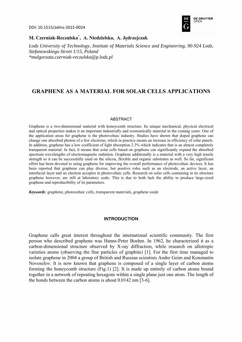
INTRODUCTION Graphene calls great interest throughout the international scientific community. The first person who described graphene was Hanns-Peter Boehm. In 1962, he characterized it as a carbon-dimensional structure observed by X-ray diffraction, while research on allotropic varieties atoms (observing the fine particles of graphite) [1]. For the first time managed to isolate graphene in 2004 a group of British and Russian scientists Andre Geim and Konstantin Novoselov. It is now known that graphene is composed of a single layer of carbon atoms forming the honeycomb structure (Fig.1) [2]. It is made up entirely of carbon atoms bound together in a network of repeating hexagons within a single plane just one atom. The length of the bonds between the carbon atoms is about 0.0142 nm [3-6].
68 ADVANCES IN MATERIALS SCIENCE, Vol. 15, No. 4 (46), December 2015
Fig.1. Structure of graphene [2]
The strongest bond in nature, the C-C bond covalently locks these atoms in place giving them remarkable mechanical properties. Conducted in 2009, the study determine the elastic limit of graphene in the range of 1 TPa, and Young's modulus of 0.5 TPa. This material is 100 times stronger than steel. And if so, graphene can come into the new super durable, yet very flexible materials replacing or reinforcing plastic and metal. To be able to introduce such use graphene need to find him a suitable substrate. In nature, pure graphene is absent, because it's thin petals in the air immediately are crease or curl. What is needed is so material on which graphene could be stretched so as not to lose its mechanical properties while remaining flexible. Carried out so far studies show that as the substrate is very well suited carbide silicon, nitride boron and copper. When the researchers will manage to overcome the problem of graphene settle on a suitable substrate and hence the possibility of using it on an industrial scale, will have a new generation of composite materials. They can then be used for the production of car bodies and aircraft [7-10].
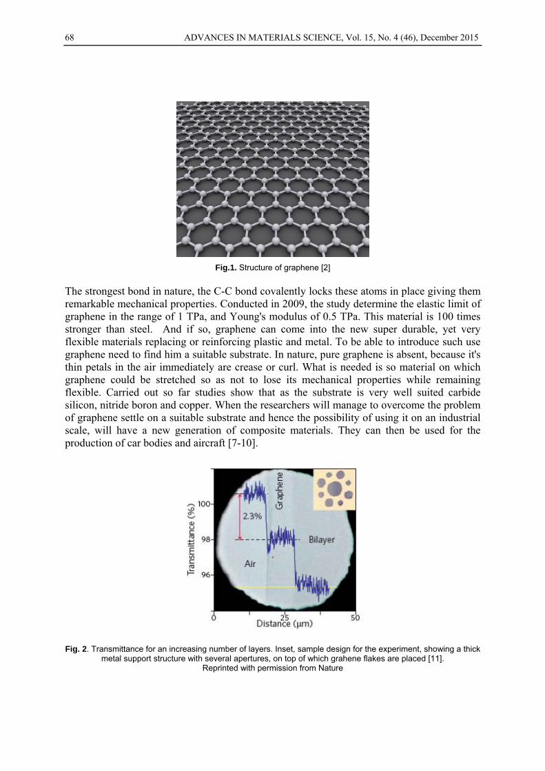
Fig. 2. Transmittance for an increasing number of layers. Inset, sample design for the experiment, showing a thick metal support structure with several apertures, on top of which grahene flakes are placed [11].
Reprinted with permission from Nature
M. Czerniak-Reczulska, A. Niedzielska, A. Jędrzejczak: Graphene as a material for solar cells … 69
Heat ranged from 4840 ± 440 to 5300 ± 480 W / mK, which is more than double that for diamond (whose thermal conductivity is from 900 to 2320 W / mK). Moreover, in its pure form it conducts electrons faster at room temperature than any other substance. Graphite is also resistant to mechanical stress. It can be stretched by 20 percent without the risk of rupturing. Graphene is also extremely thin. Instruments made from graphene could be the thinnest objects imaginable. At the same time graphene is transparent, one layer absorbs about 2,3 % light (Fig.2) [11]. Additionally, graphene has a flat transmittance spectrum from the ultraviolet (UV) region to the long wave length infrared (IR) region [12].
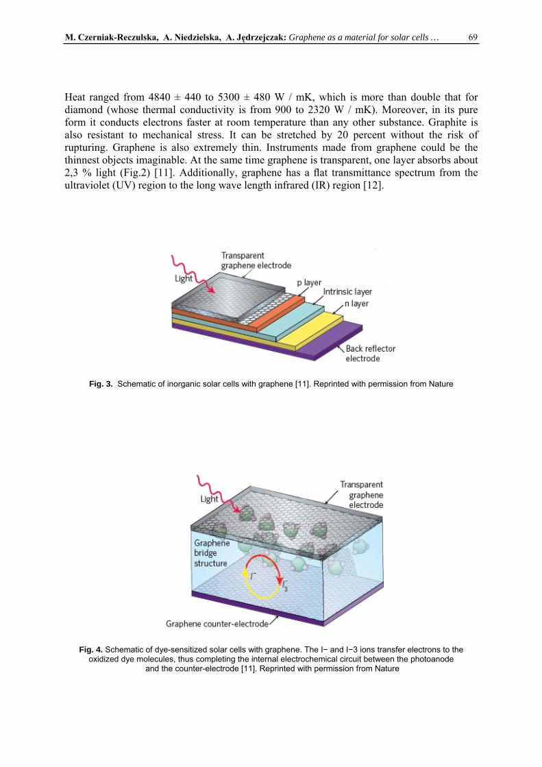
Fig. 3. Schematic of inorganic solar cells with graphene [11]. Reprinted with permission from Nature
Fig. 4. Schematic of dye-sensitized solar cells with graphene. The I− and I−3 ions transfer electrons to the
oxidized dye molecules, thus completing the internal electrochemical circuit between the photoanode and the counter-electrode [11]. Reprinted with permission from Nature
70 ADVANCES IN MATERIALS SCIENCE, Vol. 15, No. 4 (46), December 2015
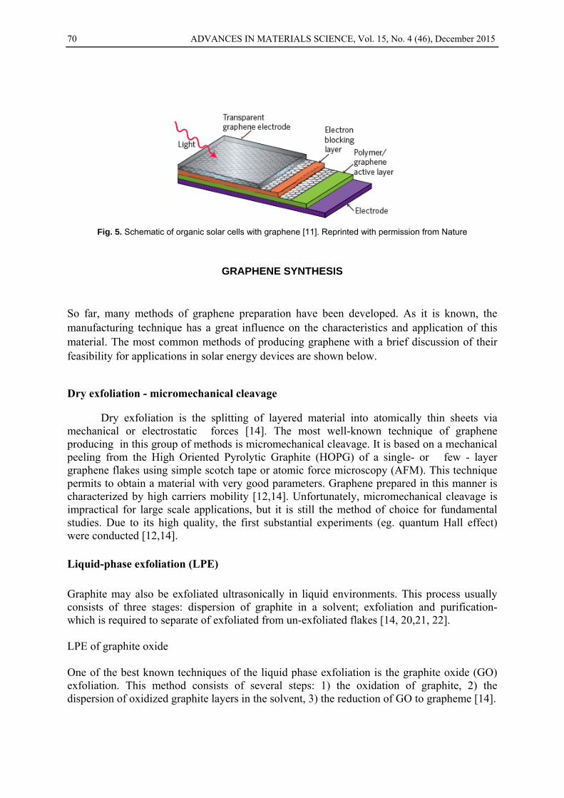
Fig. 5. Schematic of organic solar cells with graphene [11]. Reprinted with permission from Nature
GRAPHENE SYNTHESIS
So far, many methods of graphene preparation have been developed. As it is known, the manufacturing technique has a great influence on the characteristics and application of this material. The most common methods of producing graphene with a brief discussion of their feasibility for applications in solar energy devices are shown below.
Dry exfoliation - micromechanical cleavage
Dry exfoliation is the splitting of layered material into atomically thin sheets via mechanical or electrostatic forces [14]. The most well-known technique of graphene producing in this group of methods is micromechanical cleavage. It is based on a mechanical peeling from the High Oriented Pyrolytic Graphite (HOPG) of a single- or few - layer graphene flakes using simple scotch tape or atomic force microscopy (AFM). This technique permits to obtain a material with very good parameters. Graphene prepared in this manner is characterized by high carriers mobility [12,14]. Unfortunately, micromechanical cleavage is impractical for large scale applications, but it is still the method of choice for fundamental studies. Due to its high quality, the first substantial experiments (eg. quantum Hall effect) were conducted [12,14]. Liquid-phase exfoliation (LPE) Graphite may also be exfoliated ultrasonically in liquid environments. This process usually consists of three stages: dispersion of graphite in a solvent; exfoliation and purification- which is required to separate of exfoliated from un-exfoliated flakes [14, 20,21, 22]. LPE of graphite oxide One of the best known techniques of the liquid phase exfoliation is the graphite oxide (GO) exfoliation. This method consists of several steps: 1) the oxidation of graphite, 2) the dispersion of oxidized graphite layers in the solvent, 3) the reduction of GO to grapheme [14].
M. Czerniak-Reczulska, A. Niedzielska, A. Jędrzejczak: Graphene as a material for solar cells … 71
Graphite is oxidized using Hummer method by its reaction with sodium nitrite in sulfuric acid and potassium permanganate. GO flakes can be produced via sonification, thermal expansion or stirring of graphite oxide [21]. Graphite oxide is luminescent under continuous wave irradiation. Visible excitation gives a broad photoluminescence spectrum from visible to nearinfrared, while blue emission is detected upon ultraviolet excitation. This makes GO an interesting material for bio-imaging and lighting applications (e.g. light emitting devices). Till date, several reports have been demonstrated on the application of GO for organic solar cells, organic memory devices, Li ion batteries, and many more [12,14,21]. In order to reduce the graphite oxide are used methods which involves treatments by hydrazine, hydrides, p-phenylene, hydroquinone, as well as dehydration or thermal reduction. Graphite oxide and reduced graphite oxide (rGO) can be deposited on different substrates. GO and rGO are ideal for composites, due the presence of functional groups, which can link polymer. However, this method of graphene production has several short-comings, such as small yield, defective structure, and incomplete reduction of graphene, which readily degrade the graphene properties. LPE of intercalated graphite
Another known technique of exfoliation in the liquid phase is graphite intercalation. Intercalated graphite is formed by periodic insertion of atomic or molecular species (intercalants) between graphite layers. Intercalated graphene is classified in terms of ”staging” index m which is the number of graphene layers between two intercalant layers [12,14]. Thus, e.g., a stage 3 intercalated graphene has each 3 adjacent graphene layers sandwiched by 2 intercalant layers. It should be emphasized, that intercalation of atoms or molecules with different m gives rise to a wide variety of magnetic, electrical and thermal properties. Intercalated graphene have potential as highly conductive material [12]. For the intercalation of graphite alkali metal ions are used. The major types of alkali metal ions are Li, Na, K, and Cs. The main reason for the use of such ions is the fact that these ions readily react to form intercalated graphite structure. Intercalation requires a high vapor pressure (i.e., ~3 – 5 atm) to enable intercalants to penetrate between the graphite layers [12,14]. The exfoliation process of intercalated graphene is often called “spontaneous” due to the absence of ultrasonication, but it requires mechanical energy, frequently provided by stirring. To date it is possible to exfoliate of intercalated graphene to give flakes with lateral sizes ~20 µm and mobilities of ~tens cm2 V−1s-1. Liquid- phase exfoliation of intercalated graphene is time consuming process. Thus obtained graphene has tendency to oxidize [12,14]. Growth on SiC One of the techniques for producing graphene on a SiC substrate is sublimation. It involves annealing of SiC at high temperature, typically above 1300°C, in which the silicon sublimates. As a result, the carbon on the surface is formed. Whilst maintaining the relevant parameters of the process, carbon can create the structure of grapheme [14,19]. Another technique for the preparation of graphene on a SiC substrate is the carbon deposition from the gas phase (CVD), so-called vapor phase epitaxy. This method involves stopping the sublimation by using a suitable flow of argon in the reactor and the deposition of carbon films from a hydrocarbon (eg. propane) added to the carrier gas [19]. The size of thus produced graphene is limited only by the size of the used substrate.

72 ADVANCES IN MATERIALS SCIENCE, Vol. 15, No. 4 (46), December 2015
Unfortunately, graphene grown on SiC is strongly influenced by the substrate and therefore is highly sensitive to imperfections. In addition the transfer of graphene from SiC to other substrate is difficult. Therefore these restrict the using of such produced graphene for solar cell applications [12,14,19]. Synthesis by chemical vapor deposition method Another well known method is the preparation of graphene by chemical vapor deposition method (CVD) on metallic substrates (Cu, Ni, s Pt, Pd, Ru, Ir, Co itp.) [15,16,25]. Thus obtained layers can be transferred to non-metallic substrates, such as, for example silicon covered by a SiO2 layer, or organic materials. The formation of graphene on metallic substrates through CVD follows a two-step mechanism. The first step is the dilution or incorporation of carbon into the metal, which is then followed by the formation of a graphene through rapid cooling, also known as segregation [14-16,25]. Graphene grown on metals seems to be ideal for use in transparent electronics - such as for the construction of solar cells, touch screens and similar applications, using transparency and conductivity of graphene. This method for manufacturing graphene is inexpensive and can be used on a mass scale. Although large-scale graphene can be obtained by the CVD process, however, achieving large-scale homogeneous layer of graphene is still under challenge. Additionally, grain boundaries and ripples formation in graphene during synthesis processes causes defect formation in graphene. Hence, those defects create a major charge scattering and deteriorate graphene’s optical, electrical and thermal properties [12].
The growth of a polycrystalline graphene from a liquid phase
A promising method for manufacturing graphene is the synthesis from liquid metallic phase [15, 23,24]. The preparation of polycrystalline graphene from the liquid phase consist of following stages. In the first step the multilayer metal substrate - a composite of Cu / Ni (72% Cu, 28% Ni) is formed. Then, the composite is heated to a temperature of 1200 – 1250°C in an atmosphere of argon at a pressure of 100 kPa. In the next step the gas mixture with the following chemical composition is given: acetylene, hydrogen and ethylene in the ratio of 2: 1: 2, at a pressure of 3kPa [15]. Prepared in this manner graphene has high homogeneity in terms of the number of carbon layers and the degree of defect, compared to CVD graphene. Such a high homogeneity is due to atomically smooth surface of the substrate used in the synthesis process [15,23,24]. Single graphene flakes, depending on the production parameters may reach the size from several micrometers to even 1 mm [15]. This method can be used on a mass scale, and the dimensions of the prepared graphene are limited only by the size of the substrate.
PARAMETERS CHARACTERIZING A SOLAR CELLS
The most important parameters a characterizing the properties of photovoltaic cells are:
- current-voltage characteristic [Fig.] - current density (Jsc) [mA / cm2] - the open-circuit voltage (Voc) [V]
M. Czerniak-Reczulska, A. Niedzielska, A. Jędrzejczak: Graphene as a material for solar cells … 73
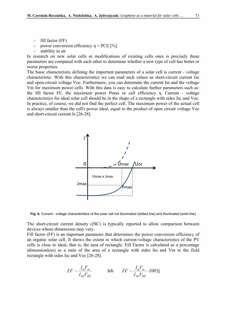
- fill factor (FF) - power conversion efficiency η = PCE [%] - stability in air
In research on new solar cells or modifications of existing cells ones is precisely these parameters are compared with each other to determine whether a new type of cell has better or worse properties. The basic characteristic defining the important parameters of a solar cell is current - voltage characteristic. With this characteristics we can read such values as short-circuit current Isc and open-circuit voltage Voc. Furthermore, you can determine the current Im and the voltage Vm for maximum power cells. With this data is easy to calculate further parameters such as: the fill factor FF, the maximum power Pmax or cell efficiency η. Current - voltage characteristics for ideal solar cell should be in the shape of a rectangle with sides Isc and Voc. In practice, of course, we did not find the perfect cell. The maximum power of the actual cell is always smaller than the cell's power ideal, equal to the product of open circuit voltage Voc and short-circuit current Is [26-28].
Pmax
Uoc Umax
Umax x Jmax
Jmax
J
0
Fig. 6. Current - voltage characteristics of the solar cell not illuminated (dotted line) and illuminated (solid line)
The short-circuit current density (JSC) is typically reported to allow comparison between devices whose dimensions may vary. Fill factor (FF) is an important parameter that determines the power conversion efficiency of an organic solar cell. It shows the extent to which current-voltage characteristics of the PV cells is close to ideal, that is, the area of rectangle. Fill Factor is calculated as a percentage (dimensionless) as a ratio of the area of a rectangle with sides Im and Vm to the field rectangle with sides Isc and Voc [26-28].
74 ADVANCES IN MATERIALS SCIENCE, Vol. 15, No. 4 (46), December 2015
Power conversion efficiency η = PCE is the ratio of the maximum power recovery in the cell to the radiation power of sunlight falling on the cell. It can be calculated with the following formula:
η- efficiency of the cell, J - the intensity of the radiation incident on the cell [W/m2] S - the surface area of the cell [m2]
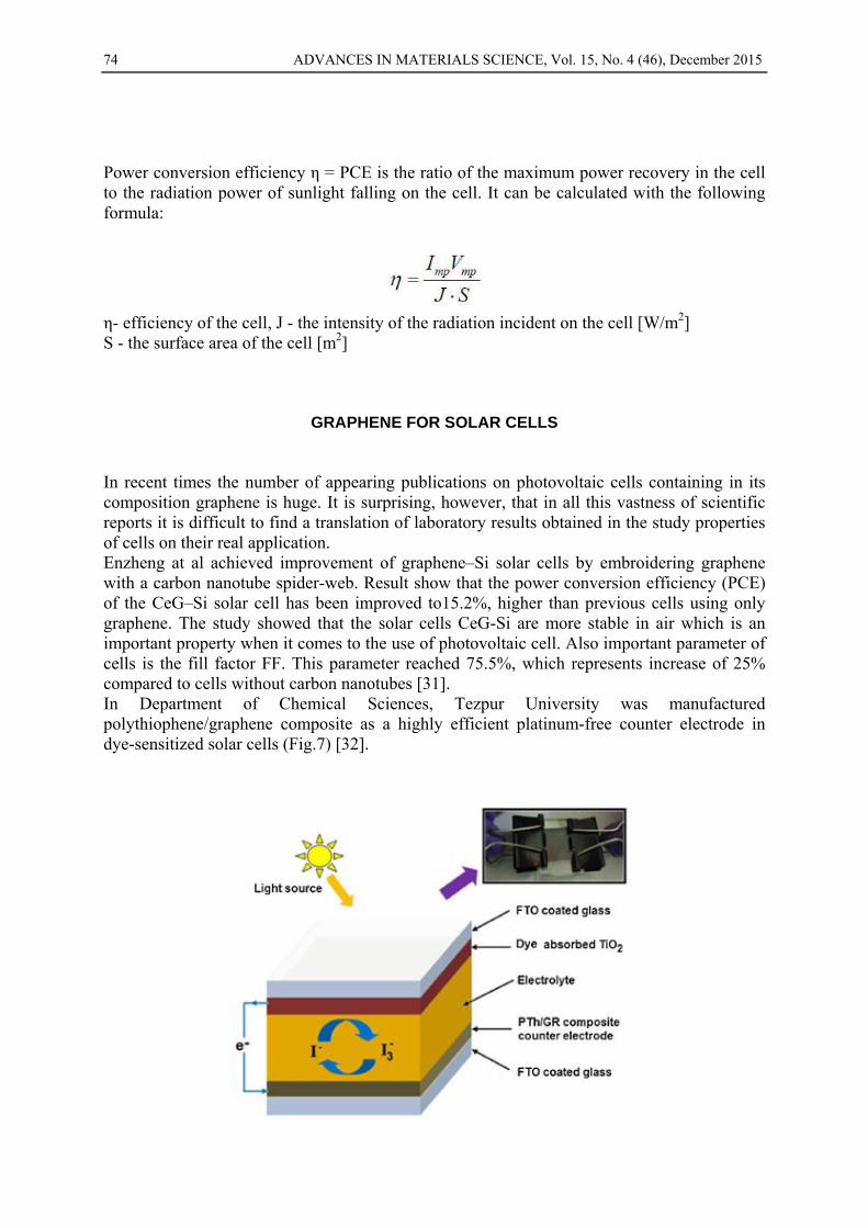
GRAPHENE FOR SOLAR CELLS In recent times the number of appearing publications on photovoltaic cells containing in its composition graphene is huge. It is surprising, however, that in all this vastness of scientific reports it is difficult to find a translation of laboratory results obtained in the study properties of cells on their real application. Enzheng at al achieved improvement of graphene–Si solar cells by embroidering graphene with a carbon nanotube spider-web. Result show that the power conversion efficiency (PCE) of the CeG–Si solar cell has been improved to15.2%, higher than previous cells using only graphene. The study showed that the solar cells CeG-Si are more stable in air which is an important property when it comes to the use of photovoltaic cell. Also important parameter of cells is the fill factor FF. This parameter reached 75.5%, which represents increase of 25% compared to cells without carbon nanotubes [31]. In Department of Chemical Sciences, Tezpur University was manufactured polythiophene/graphene composite as a highly efficient platinum-free counter electrode in dye-sensitized solar cells (Fig.7) [32].
M. Czerniak-Reczulska, A. Niedzielska, A. Jędrzejczak: Graphene as a material for solar cells … 75
Fig. 7. Schematic diagram for assembly of DSSCs based on PTh/GR composite [32]. Reprinted with permission from Nano Energy
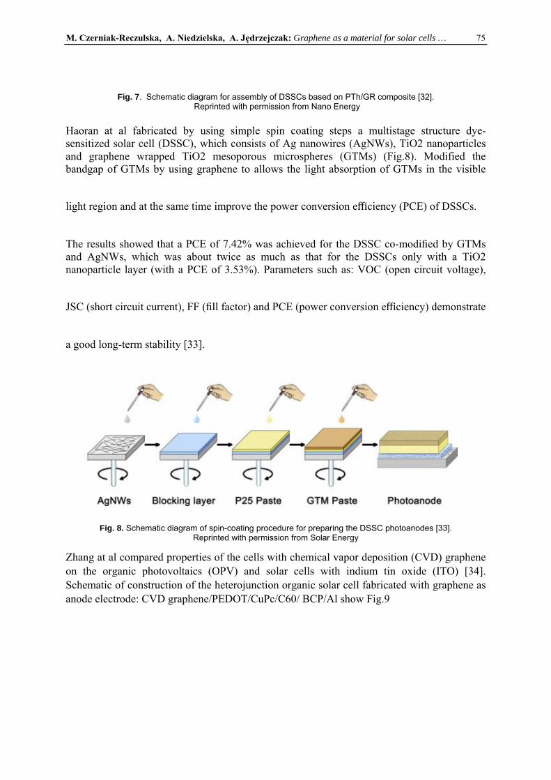
Haoran at al fabricated by using simple spin coating steps a multistage structure dye-sensitized solar cell (DSSC), which consists of Ag nanowires (AgNWs), TiO2 nanoparticles and graphene wrapped TiO2 mesoporous microspheres (GTMs) (Fig.8). Modified the bandgap of GTMs by using graphene to allows the light absorption of GTMs in the visible
light region and at the same time improve the power conversion efficiency (PCE) of DSSCs.
The results showed that a PCE of 7.42% was achieved for the DSSC co-modified by GTMs and AgNWs, which was about twice as much as that for the DSSCs only with a TiO2 nanoparticle layer (with a PCE of 3.53%). Parameters such as: VOC (open circuit voltage),
JSC (short circuit current), FF (fill factor) and PCE (power conversion efficiency) demonstrate
a good long-term stability [33].
Fig. 8. Schematic diagram of spin-coating procedure for preparing the DSSC photoanodes [33]. Reprinted with permission from Solar Energy
Zhang at al compared properties of the cells with chemical vapor deposition (CVD) graphene on the organic photovoltaics (OPV) and solar cells with indium tin oxide (ITO) [34]. Schematic of construction of the heterojunction organic solar cell fabricated with graphene as anode electrode: CVD graphene/PEDOT/CuPc/C60/ BCP/Al show Fig.9
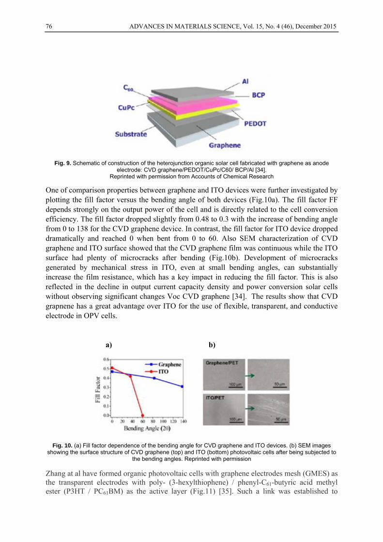
76 ADVANCES IN MATERIALS SCIENCE, Vol. 15, No. 4 (46), December 2015
Fig. 9. Schematic of construction of the heterojunction organic solar cell fabricated with graphene as anode electrode: CVD graphene/PEDOT/CuPc/C60/ BCP/Al [34].
Reprinted with permission from Accounts of Chemical Research
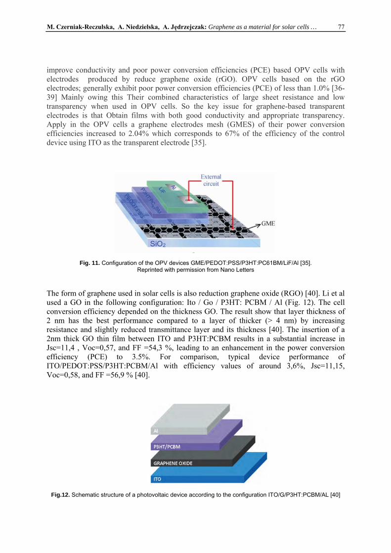
One of comparison properties between graphene and ITO devices were further investigated by plotting the fill factor versus the bending angle of both devices (Fig.10a). The fill factor FF depends strongly on the output power of the cell and is directly related to the cell conversion efficiency. The fill factor dropped slightly from 0.48 to 0.3 with the increase of bending angle from 0 to 138 for the CVD graphene device. In contrast, the fill factor for ITO device dropped dramatically and reached 0 when bent from 0 to 60. Also SEM characterization of CVD graphene and ITO surface showed that the CVD graphene film was continuous while the ITO surface had plenty of microcracks after bending (Fig.10b). Development of microcracks generated by mechanical stress in ITO, even at small bending angles, can substantially increase the film resistance, which has a key impact in reducing the fill factor. This is also reflected in the decline in output current capacity density and power conversion solar cells without observing significant changes Voc CVD graphene [34]. The results show that CVD grapnene has a great advantage over ITO for the use of flexible, transparent, and conductive electrode in OPV cells.
a) b)
Fig. 10. (a) Fill factor dependence of the bending angle for CVD graphene and ITO devices. (b) SEM images showing the surface structure of CVD graphene (top) and ITO (bottom) photovoltaic cells after being subjected to
the bending angles. Reprinted with permission
Zhang at al have formed organic photovoltaic cells with graphene electrodes mesh (GMES) as the transparent electrodes with poly- (3-hexylthiophene) / phenyl-C61-butyric acid methyl ester (P3HT / PC61BM) as the active layer (Fig.11) [35]. Such a link was established to
M. Czerniak-Reczulska, A. Niedzielska, A. Jędrzejczak: Graphene as a material for solar cells … 77
improve conductivity and poor power conversion efficiencies (PCE) based OPV cells with electrodes produced by reduce graphene oxide (rGO). OPV cells based on the rGO electrodes; generally exhibit poor power conversion efficiencies (PCE) of less than 1.0% [36-39] Mainly owing this Their combined characteristics of large sheet resistance and low transparency when used in OPV cells. So the key issue for graphene-based transparent electrodes is that Obtain films with both good conductivity and appropriate transparency. Apply in the OPV cells a graphene electrodes mesh (GMES) of their power conversion efficiencies increased to 2.04% which corresponds to 67% of the efficiency of the control device using ITO as the transparent electrode [35].
Fig. 11. Configuration of the OPV devices GME/PEDOT:PSS/P3HT:PC61BM/LiF/Al [35].
Reprinted with permission from Nano Letters
The form of graphene used in solar cells is also reduction graphene oxide (RGO) [40]. Li et al used a GO in the following configuration: Ito / Go / P3HT: PCBM / Al (Fig. 12). The cell conversion efficiency depended on the thickness GO. The result show that layer thickness of 2 nm has the best performance compared to a layer of thicker (> 4 nm) by increasing resistance and slightly reduced transmittance layer and its thickness [40]. The insertion of a 2nm thick GO thin film between ITO and P3HT:PCBM results in a substantial increase in Jsc=11,4 , Voc=0,57, and FF =54,3 %, leading to an enhancement in the power conversion efficiency (PCE) to 3.5%. For comparison, typical device performance of ITO/PEDOT:PSS/P3HT:PCBM/Al with efficiency values of around 3,6%, Jsc=11,15, Voc=0,58, and FF =56,9 % [40].
Fig.12. Schematic structure of a photovoltaic device according to the configuration ITO/G/P3HT:PCBM/AL [40]
78 ADVANCES IN MATERIALS SCIENCE, Vol. 15, No. 4 (46), December 2015
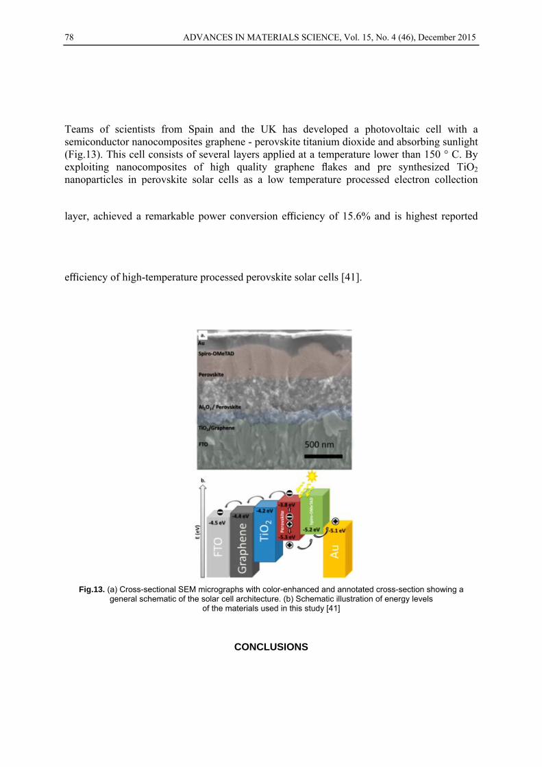
Teams of scientists from Spain and the UK has developed a photovoltaic cell with a semiconductor nanocomposites graphene - perovskite titanium dioxide and absorbing sunlight (Fig.13). This cell consists of several layers applied at a temperature lower than 150 ° C. By exploiting nanocomposites of high quality graphene flakes and pre synthesized TiO2 nanoparticles in perovskite solar cells as a low temperature processed electron collection
layer, achieved a remarkable power conversion efficiency of 15.6% and is highest reported
efficiency of high-temperature processed perovskite solar cells [41].
Fig.13. (a) Cross-sectional SEM micrographs with color-enhanced and annotated cross-section showing a
general schematic of the solar cell architecture. (b) Schematic illustration of energy levels of the materials used in this study [41]
CONCLUSIONS
M. Czerniak-Reczulska, A. Niedzielska, A. Jędrzejczak: Graphene as a material for solar cells … 79
In this article, we present the use of graphene in dye-sensitized solar cells, organic solar cells, Si solar cells, perovskite solar cells. Graphene was added to the cells in various forms: they were both graphene flakes, graphene single and multi-layered graphene oxide. Conducting research into the properties of graphene in solar cells apply only on a laboratory scale. To be able to examine the behavior of photovoltaic modules under real conditions must be defeated the problems, which relate to: producing large-sized graphene with reproducible properties, no defects, the high stability. A promising method for manufacturing a graphene on just such parameters appear to be the synthesis from liquid metallic phase method. Another important aspect is possibility to produce graphene on various substrates to eliminate the problems that arise during the transfer of graphene from one material to another.
REFERENCES
1. Boehm H.P., Setton R., Stumpp E. Nomenclature and terminology of graphite intercalation
compounds, Pure and Applied Chemistry 66 (1994), 1893-1901.
2. Centrum grafenu i innowacyjnych technologii; Biuletyn Politechniki Warszawskiej; 2014.
3. Scientific American nr 298, Carbon Wonderland, 2008, 90-97.
4. Science nr 324, Graphene: Status and prospects (2009), 1530-1534.
5. http://nobelprize.org/nobel_prizes/physics/laureates/2010/sciback_phy_10_2.pdf.
6. Novoselov K.S. et al., Two-dimensional atomic crystals, Proc. Natl Acad. Sci., USA.
7. Ghavanini F.A., Theander H., Graphene feasibility and foresight study for transport infrastructures; Chalmers Industriteknik 2015.
8. Kumar N.A., Dar M.A., Gul R. Jong-Beom Baek, Graphene and molybdenum disulfide hybrids: synthesis and applications; Materials Today 18(5) (2015).
9. Soldano C., Mahmood A., Dujardin E., Production, properties and potential of grapheme; Carbon 48 (2010), 2127-2150.
10. Frank IW, Tanenbum DM, Van der Zande AM, McEuen P., Mechanical properties of suspensed grapheme sheets, In 51st International conference on electron, ion, and phton beam technology and nanofabrication, AVS Amer Inst Physics 207, 2558-2561.
11. Bonaccorso F., Sun Z., Hasan T., Ferrari A.C., Nature photonics, 2010.
12. Santanu Das, Pitchaimuthu Sudhagar and Yong Soo Kang, Wonbong Choia; Graphene synthesis and application for solar cells; J. Mater. Res. 2013.
13. Stankovich S., Dikin D., Dommett G., Kohlhaas K., Zimney E, Stach E., Piner R., SonBinh T. Nguyen and Ruoff R., Graphene-based composite materials; Nature 442 (2006), 282-286.
14. Bonaccorso F., Lombardo A., Hasan T., Sun Z., Colombo L., Ferrari A.C., Production and processing of graphene and 2d crystals; Materials Today 15(12) (2012), 564-589.
15. Choon-Ming S., Siang-Paiao Chai, Abdul Rahman Mohamed; Mechanisms of graphene growth by chemical vapour deposition on transition metals, Carbon 70, 1-21 (2014).
16. Mattevi C., Kim H., Chhowalla M., A review of chemical vapour deposition of grapheme on copper, , J. Mater. Chem., 21, 3324-3334, (2011).
80 ADVANCES IN MATERIALS SCIENCE, Vol. 15, No. 4 (46), December 2015
17. Kula P., Pietrasik R., Dybowski K., Atraszkiewicz R., Kaczmarek L., Kazimierski D., Niedzielski P., Modrzyk W., The growth of a polycrystalline graphene from a liquid phase, Nanotech 1 (2013), 210 - 212.
18. Chung K., Lee C.H,. Yi G.C., Transferable GaN Layers Grown on ZnO-Coated Graphene Layers for Optoelectronic Devices Science 330 (2010) 655-657.
19. Tetlow H., Posthuma de Boer J. et al; Growth of epitaxial graphene: Theory and experiment, Physics reports, 542 (2014), 195-295.
20. Hasan, T., Solution‐phase exfoliation of graphite for ultrafast photonics, Phys Status Solidi B.
247 (2010) 2953-2957.
21. Liao K.H., Mittal A., Bose S., Leighton C., Mkhoyan K.A., Macosko C.V., Aqueous only route toward graphene from graphite oxide, ACS Nano 5 (2011), 1253-1258.
22. Wang H. J., Robinson J., Li X., Dai., Solvothermal Reduction of Chemically Exfoliated Graphene Sheets, J. Am. Chem. Soc. 131 (2009), 9910-9911.
23. Hiura H., Lee M.V., Tyurnina A.V., Tsukagoshi K., Liquid phase growth of graphene on silicon carbide, Carbon 50 (2012), 5076–5084.
24. Kolodziejczyk L., Kula P., Szymański W., Atraszkiewicz R., Dybowski K., Pietrasik R., Frictional behaviour of polycrystalline graphene grown on liquid metallic matrix, Tribology International 12 (2014), 003.
25. Zhang Y., Zhang L., Zhou C., Review of Chemical Vapor Deposition of Graphene and Related Applications, Acc. Chem. Res. 46 (2013), 2329–2339.
26. Markvart T., Castaner L., Solar Cells: Materials, Manufacture and Operation; Elsevier, Oxford 2005.
27. Jarzębski Z.M., Energia słoneczna, konwersja fotowoltaiczna. Państwowe Wydawnictwo Naukowe, Warszawa 1990.
28. Centurioni E., Summonte C., Optical an open source program for the optical simulation of multilayer systems, 22th EPVSEC, Milano, Italy 2007.
29. Park H, Chang S., Smith M., Gradecak S., Kong J., Interface engineering of grapheme for universal applications as both anode and cathode in organic photovoltaics, Scientific reports 3 (2013), 1581- 2013.
30. Shia E., Lib H., Xua W., Wua S., Weic J., Fang F., Cao A., Improvement of graphene–Si solar cells by embroidering grapheme with a carbon nanotube spider-web; Nano Energy 2015 – article in press.
31. Chandramika Bora, Chandrama Sarkar, Kiron J. Mohan, Swapan Dolui; Polythiophene /graphene composite as a highly efficient platinum-free counter electrode in dye-sensitized solar cells , Electrochimica Acta 03/2015; 157.
32. Yan H., Wang J., Feng B, Duan K, Weng J., Graphene and Ag nanowires co-modified
photoanodes for high-efficiency dye-sensitized solar cells, Solar Energy 122 (2015), 966–975.
M. Czerniak-Reczulska, A. Niedzielska, A. Jędrzejczak: Graphene as a material for solar cells … 81
33. Review of Chemical Vapor Deposition of Graphene and Related Applications, Accounts of Chemical Research; 46(10) (2013) 2329–2339.
34. Qian Zhang, Xiangjian Wan, Fei Xing, Lu Huang, Guankui Long, Ningbo Yi, Wang Ni, Zhibo Liu, Jianguo Tian, Yongsheng Chen: Solution-processable graphene mesh transparent electrodes for organic solar cells. Nano Lett. 6(7) (2013), 478-484.
35. Xu, Y.; Long, G.; Huang, L.; Huang, Y.; Wan, X.; Ma, Y.; Chen, Y. Polymer photovoltaic devices with transparent graphene electrodes produced by spin-casting. Carbon 48 (2010), 3308–3311.
36. Wu, J.; Becerril, H. A.; Bao, Z.; Liu, Z.; Chen, Y.; Peumans, P. Organic solar cells with solution-processed graphene transparent electrodes. Appl. Phys. Lett., 92 (2008), 263-302.
37. Eda, G.; Lin, Y. Y.; Miller, S.; Chen, C. W.; Su, W. F.; Transparent and conducting electrodes for organic electronics from reduced graphene oxide. Appl. Phys. Lett., 92 (2008), 233-305.
38. Jung, V. C.; Chen, L. M.; Allen, M. J.; Wassei, J. K.; Nelson, K.; Kaner, R. B.; Yang, Y. Low-temperature solution processing of graphene–carbon nanotube hybrid materials for high-performance transparent conductors. Nano Lett., 9 (2009), 1949–1955.
39. Shao-Sian Li,Kun-Hua Tu,Chih-Cheng Lin,Chun-Wei Chen,and Manish Chhowalla; Solution-processable grapheme oxide as an efficient hole transport layer in polymer solar cells; American Chemical Society 4 (6), 3169-3174
40. Jacob Tse-Wei Wang, James M. Ball, Eva M. Barea, Antonio Abate, Jack A. Alexander-Webber, Jian Huang, Michael Saliba, Ivan Mora-Sero, Juan Bisquert, Henry J. Snaith, and Robin J. Nicholas; Low-Temperature Processed Electron Collection Layers of Graphene / TiO2 Nanocomposites in Thin Film Perovskite Solar Cells; Nano Letters, 14 (2014), 724−730.
41. Shemella P., Nayak S.K., Electronic structure and band-gap modulation of graphene via substrate surface chemistry. Appl. Phys. Lett. 94, (2009), 032-101
42. Chang D.W., Choi H.J., Filer A., Baek J.B., Journal of Materials Chemistry A, 31, 2014.
43. Bernardi M., Palummo M., Grossman J.C., Extraordinary Sunlight Absorption and One Nanometer Thick Photovoltaics Using Two-Dimensional Monolayer Materials, Nano letters, 2013.