single source precursor-based hv-mocvd deposition of binary group 13-antimonide thin films
TRANSCRIPT

201 (2007) 9071–9075www.elsevier.com/locate/surfcoat
Surface & Coatings Technology
Single source precursor-based HV-MOCVD deposition ofbinary group 13-antimonide thin films
Stephan Schulz a,⁎, Sonja Fahrenholz a, Daniella Schuchmann a, Andreas Kuczkowski a,Wilfried Assenmacher b, Frank Reilmann c, Naoufal Bahlawane c, Katharina Kohse-Höinghaus c
a Department of Chemistry, University of Paderborn, Warburger Str. 100, D-33095 Paderborn, Germanyb Department of Chemistry, University of Bonn, Inorganic Chemisty I, Römerstr. 164, D-53117 Bonn, Germany
c Department of Chemistry, University of Bielefeld, Universitätsstr. 25, D-33615 Bielefeld, Germany
Available online 31 March 2007
Abstract
Tailor-made single source precursors of the type [R2GaSbR′2]x (R, R′=alkyl) have been prepared by a novel synthetic pathways. According totheir very low vapor pressures, a specifically designed HV-MOCVD reactor was built, which can be used for the deposition of GaSb materialfilms. The influence of several process parameters such as substrate temperature and reactor geometry on the quality of the resulting films will bediscussed.© 2007 Elsevier B.V. All rights reserved.
Keywords: Organometallic CVD; Gallium antimonide; Compound semiconductors
1. Introduction
Group 13-antimonides MSb (M=Al, Ga, In) are attractivematerials for electronic and optoelectronic applications operatingin the infra-red regime such as thermophotovoltaic and opto-electronic devices due to their small band gaps and high electronmobilities [1]. Unfortunately, the deposition of MSb materialfilms byMOCVD-process [2], which is well established for high-throughput and low-cost production of III–V material films, israther problematic due to the lack of suitable precursors [3]. SbH3,which is the most ideal Sb-source since it contains no carbon-based organic ligand, is thermally too unstable even though its usewas recently described [4]. Furthermore, the lowmelting points ofthe antimonides MSb (e.g. InSb 525 °C) limits the growth of suchfilms starting with thermally stable organometallic precursorssuch as MMe3 (M=Al, Ga, In), which require high substratetemperatures to ensure their complete decomposition, while lowdeposition temperatures are imposed by the selective evaporationof the grown film. Therefore, the allowed range of depositiontemperature is very narrow and, as a consequence, MSb films
⁎ Corresponding author. Tel.: +49 05251 602493; fax: +49 05251 603423.E-mail address: [email protected] (S. Schulz).
0257-8972/$ - see front matter © 2007 Elsevier B.V. All rights reserved.doi:10.1016/j.surfcoat.2007.03.045
are typically grown in the kinetically-controlled regime due to anincomplete decomposition of the precursors [5]. In addition, thelow vapor pressure of elemental antimony requires a precisecontrol of the SbR3:GaR3 (V:III) molar ratio less or near unityin order to avoid the deposition of an excess of elemental Sb [6].The as-described problems have lead to an increased searchfor alternate precursors and several candidates, including i-Pr3Sb,i-Pr2SbH, Sb(NMe2)3, t-Bu3Al and Me2(Et)N–AlH3, have beenfound to produce MSb films of good quality [7].
An alternate loophole to solve the temperature problem and tocontrol the V:III molar ratio makes use of so-called single sourceprecursors, kinetically stabilized molecules which contain theelements of the desired material, e.g. Ga and Sb, connected bya stable chemical bond [8]. Typical single source precursorssuch as Lewis acid–base adducts R3M-ER′3 and heterocycles[R2MER′2]x have been identified as reaction intermediates inclassical MOCVD processes as was shown for the deposition ofInP from InMe3 and PH3 and of AlN from AlMe3 and NH3 [9].Their metal–carbon bond energies are lower compared to puremetal trialkyls, allowing lower deposition temperatures. Binarygroup 13-nitrides and -phosphides have been grown in the pastby use of single source precursors, whereas the correspondingantimonides MSb have been investigated to a far lesser extent,

Fig. 2. Photograph of the HV-MOCVD glass reactor showing the 90° orientationof the substrate.
9072 S. Schulz et al. / Surface & Coatings Technology 201 (2007) 9071–9075
most likely due to the lack of suitable precursors [10]. Typicalreaction pathways such as salt, alkane and H2-eliminationreactions, which have been established for the synthesis of group13/15 compounds containing the lighter elements of group 15(N, P, As), almost completely failed for the synthesis of theantimonides. Only within the last decade, we and others devel-oped novel reaction pathways for the synthesis of heterocyclesof the type [R2MSbR′2]x [11], with the so-called distibine cleav-age reaction as the most promising one [12].
Herein we report on our results of MOCVD deposition studiesobtained with [tBu2GaSbEt2]2 in a home-made HV-MOCVDreactor, which was optimized for air-and moisture-sensitive pre-cursors with very low vapor pressures. The influence of processparameters such as substrate temperature and reactor geometry onthe quality of the resulting GaSb material films will be discussed.
2. Discussion
Reactions of GaR3 with Sb2R′4 initially yield Lewis acid–base adducts of the type [R3M]2[Sb2R4] with the distibinemoiety serving as bidentate ligand. These adducts undergo Sb–Sb and M–C bond breakage reactions in solution at ambienttemperature with subsequent formation of the desired hetero-cycles [R2GaSbR′2]x, which either form four- or six-memberedrings. According to this general reaction sequence, the sub-stitution pattern of the molecule can easily be modified, whichallows fine-tuning of the chemical and physical properties ofthese tailor-made precursors [12].
R3Gaþ RV2Sb� SbRV2Y�RSbRV21=x R2GaSbRV2½ �x
R ¼ Me;RV¼ Me;i�PrR ¼ t�Bu;RV¼ Me;Et; n�Pr;i�Pr;i�Bu
The compounds are unexceptionally crystalline solids withmelting points far above 120 °C and possess low vapor pressures.They can be re-crystallized from solutions in non-coordinatingsolvents such as hexane or toluene. Further purification by sub-
Fig. 1. Mass spectrometric monitoring of the [t-Bu2GaSbEt2]2 thermolysis inCVD conditions showing fragments of t-BuGaMe and iso-butene as a functionof the temperature.
limation under reduced pressure (10−5 mbar) is also possible.Almost 10 potential precursors have been prepared according tothis reaction sequence, from which [t-Bu2GaSbEt2]2 has beenstudied in detail in HV-MOCVD processes. [t-Bu2GaSbEt2]2 hasa melting point of 177 °C and sublimes without decomposition at120 °C and 10−5 mbar.
[t-Bu2GaSbEt2]2 was investigated using the mass spectrom-etry method in CVD conditions. For this study, a hot-wall CVDreactor was coupled to a TOF-mass spectrometer. The evap-oration of the precursor was achieved at 130 °C, the reactorpressure was maintained at 6×10⁻⁶ mbar and the compositionof the gas phase monitored as a function of the CVD reactortemperature between 130 and 600 °C. Although ionization wasachieved with low energy of the electron beam (10 eV), severefragmentation of the precursor was observed. Some fragmentsresult from thermal decomposition, others exclusively from thefragmentation due to the electron impact (e.g. t-BuGaMe, M=141.019). These fragments were used to qualitatively monitorthe evolution of the partial pressure of the precursor as a func-tion of the temperature. Fig. 1 shows that the thermaldecomposition of the precursor is observed at a temperatureof 250 to 300 °C. It is worth noting that conventionally usedprecursors in dual-source CVD of GaSb, such as Ga(CH3)3 andSb(C2H5)3, are stable up to 400 °C. Therefore, the single sourceprecursor [t-Bu2GaSbEt2]2 is expected to allow the growth ofGaSb at lower temperatures. Among the thermolysis byproductsof [tBu2GaSbEt2]2, iso-butene (M=56.0626) and ethylene wereidentified as a result of β-H elimination processes.
GaSb films have been deposited on Si(100) substrates usinghot-wall and cold-wall HV-MOCVD reactors [13]. The latterwas built in order to optimize the deposition results, since GaSbfilms obtained with the hot-wall reactor were not uniform (seeFig. 3A). The outer mantle of this new CVD reactor is made ofglass, giving an optical control of the deposition process, andthe whole reactor can be transferred into a standard glovebox[14]. This allows both the loading of the evaporator with thesolid precursor and the handling of the deposited material filmunder inert gas conditions, which is essential in case of air- and

9073S. Schulz et al. / Surface & Coatings Technology 201 (2007) 9071–9075
moisture-sensitive precursors and materials. The heart of thenew reactor is the evaporator, were the precursor is loaded, theprecursor line and the substrate heater, which can independentlybe heated to 200 (evaporator, precursor line) and 900 °C(substrate heater), respectively. The heated precursor lineprevents the precursor from condensation at the glass walland consequently allows the transport of the gaseous precursorto the substrate. The distance of the substrate heater to theopening of the precursor line can be varied from 1 to 8 cm
Fig. 3. SEM images of GaSb films grown on Si(100) substrates at 450 °C using ahot-wall (A) and a cold-wall HV-MOCVD reactor with different substrateorientations ((B) 90°, (C) 160°).
Fig. 4. SEM images of GaSb films deposited at 400 (A), 425 (B) and 450 °C (C)on Si(100) substrates using the HV-MOCVD cold-wall reactor with optimizedsubstrate orientation B.
(distance) and the substrate to precursor line orientation from90° (orthogonal; in the future referred to as orientation A)) asshown in Fig. 2 to 180° (in line; orientation B). In addition, thereactor is equipped with a gas pipe including mass flowcontroller which allows deposition studies under a steam of inert(N2, Ar) and reactive gases such as H2. The gas pipe can also beheated up to 150 °C.
Typical SEM photographs of GaSb films deposited with thehot-wall (A) and cold-wall reactor (B/C) at a working pressure
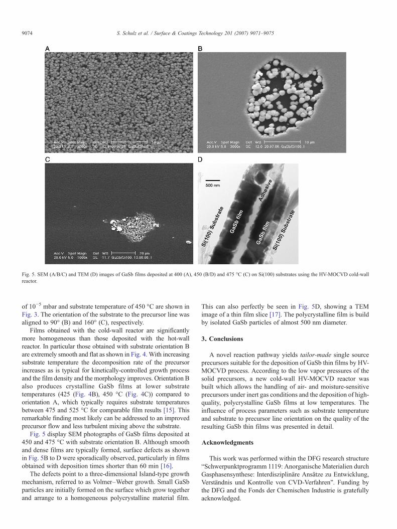
Fig. 5. SEM (A/B/C) and TEM (D) images of GaSb films deposited at 400 (A), 450 (B/D) and 475 °C (C) on Si(100) substrates using the HV-MOCVD cold-wallreactor.
9074 S. Schulz et al. / Surface & Coatings Technology 201 (2007) 9071–9075
of 10−5 mbar and substrate temperature of 450 °C are shown inFig. 3. The orientation of the substrate to the precursor line wasaligned to 90° (B) and 160° (C), respectively.
Films obtained with the cold-wall reactor are significantlymore homogeneous than those deposited with the hot-wallreactor. In particular those obtained with substrate orientation Bare extremely smooth and flat as shown in Fig. 4. With increasingsubstrate temperature the decomposition rate of the precursorincreases as is typical for kinetically-controlled growth processand the film density and the morphology improves. Orientation Balso produces crystalline GaSb films at lower substratetemperatures (425 (Fig. 4B), 450 °C (Fig. 4C)) compared toorientation A, which typically requires substrate temperaturesbetween 475 and 525 °C for comparable film results [15]. Thisremarkable finding most likely can be addressed to an improvedprecursor flow and less turbulent mixing above the substrate.
Fig. 5 display SEM photographs of GaSb films deposited at450 and 475 °C with substrate orientation B. Although smoothand dense films are typically formed, surface defects as shownin Fig. 5B to D were sporadically observed, particularly in filmsobtained with deposition times shorter than 60 min [16].
The defects point to a three-dimensional Island-type growthmechanism, referred to as Volmer–Weber growth. Small GaSbparticles are initially formed on the surface which grow togetherand arrange to a homogeneous polycrystalline material film.
This can also perfectly be seen in Fig. 5D, showing a TEMimage of a thin film slice [17]. The polycrystalline film is buildby isolated GaSb particles of almost 500 nm diameter.
3. Conclusions
A novel reaction pathway yields tailor-made single sourceprecursors suitable for the deposition of GaSb thin films by HV-MOCVD process. According to the low vapor pressures of thesolid precursors, a new cold-wall HV-MOCVD reactor wasbuilt which allows the handling of air- and moisture-sensitiveprecursors under inert gas conditions and the deposition of high-quality, polycrystalline GaSb films at low temperatures. Theinfluence of process parameters such as substrate temperatureand substrate to precursor line orientation on the quality of theresulting GaSb thin films was presented in detail.
Acknowledgments
This work was performed within the DFG research structure“Schwerpunktprogramm 1119: Anorganische Materialien durchGasphasensynthese: Interdisziplinäre Ansätze zu Entwicklung,Verständnis und Kontrolle von CVD-Verfahren”. Funding bythe DFG and the Fonds der Chemischen Industrie is gratefullyacknowledged.

9075S. Schulz et al. / Surface & Coatings Technology 201 (2007) 9071–9075
References
[1] (a) J.M. McChesney, J. Haigh, I.M. Dharmadasa, D.J. Mowthorpe, Opt.Mater. 6 (1996) 63;
(b) C. Agert, P. Lanyi, A.W. Bett, J. Cryst. Growth 225 (2001) 426.[2] (a) TheMOCVD process was initially described byManasevit et al. H.M.
Manasevit, W.I. Simpson, J. Electrochem. Soc. 116 (1969) 1725;(b) H.M. Manasevit, K.L. Hess, J. Electrochem. Soc. 126 (1979) 2031.
[3] (a) For excellent review articles see the following and references citedtherein: A. Aardvark, N.J. Mason, P.J. Walker, Prog. Cryst. GrowthCharact. 35 (1997) 207;
(b) R.M. Biefeld, Mater. Sci. Eng., R. Rep. 36 (2002) 105.[4] J.S. Foord, F.P. Howard, G.S. McGrady, G.J. Davies, J. Cryst. Growth 188
(1998) 144.[5] (a) C.A. Wang, S. Salim, K.F. Jensen, A.C. Jones, J. Cryst. Growth 170
(1997) 55;(b) J.S. Ford, F.P. Howard, G.J. Davies, J. Cryst. Growth 188 (1998) 159.
[6] (a) J. Shin, A. Verma, G.B. Stringfellow, R.W. Gedridge Jr., J. Cryst.Growth 151 (1995) 1;
(b) A. Subekti, E.M. Goldys, M.J. Paterson, K. Drozdowicz-Tomsia, T.L.Tansley, J. Mater. Res. 14 (1999) 1238;
(c) A. Subekti, E.M. Goldys, T.L. Tansley, J. Phys. Chem. Solids 61 (2000)537.
[7] (a) R.M. Biefeld, A.A. Allerman, S.R. Kurtz, J. Cryst. Growth 174 (1997)593;
(b) J. Shin, Y. Hsu, G.B. Stringfellow, R.W. Gedridge, J. Electron. Mater.24 (1995) 1563;
(c) Y.S. Chun, G.B. Stringfellow, R.W. Gedridge Jr., J. Electron. Mater.25 (1996) 1539;
(d) C.W.Wang, M.C. Finn, S. Salim, K.F. Jensen, A.C. Jones, Appl. Phys.Lett. 67 (1995) 1384;
(e) C.W. Wang, K.F. Jensen, A.C. Jones, H.K. Choi, Appl. Phys. Lett. 68(1996) 400;
(f) R.M. Biefeld, A.A. Allerman, M.W. Pelczynski, Appl. Phys. Lett. 68(1996) 932.
[8] (a) See the following a references cited therein: A.H. Cowley, R.A. Jones,Angew. Chem., Int. Ed. Engl. 28 (1989) 1208;
(b) F. Maury, Adv. Mater. 3 (1991) 542;(c) R.A. Fischer, Chem. unserer Zeit 29 (1995) 141;(d) F.C. Sauls, L.V. Interrante, Coord. Chem. Rev. 128 (1993) 193;(e) A.C. Jones, Chem. Soc. Rev. (1997) 101;(f) P. O'Brien, S. Haggata, Adv. Mater. Opt. Electron. 5 (1995) 117.
[9] (a) E.G.J. Staring, G.J.B.M. Meekes, J. Am. Chem. Soc. 111 (1989) 7648;(b) F.C. Sauls, L.V. Interrante, Z.P. Jiang, Inorg. Chem. 29 (1990) 2989.
[10] (a) Prior to our initial studyH.S. Park, S. Schulz, H.Wessel, H.W. Roesky,Chem. Vap. Depos. 5 (1999) 179;
(b) S. Schulz, S. Fahrenholz,A.Kuczkowski,W.Assenmacher,A.Seemayer,K.Wandelt, Chem. Mater. 17 (2005) 1982, Cowley et al. reported on thedeposition of MSb-films using [Me2MSb(t-Bu)2]3 (M = Ga, In);A.H. Cowley, R.A. Jones, C.M. Nunn, D.L. Westmoreland, Chem.Mater. 2 (1990) 221.
[11] See for instance: S. Schulz, Adv. Organomet. Chem. 49 (2003) 225.[12] (a) A. Kuczkowski, S. Schulz, M. Nieger, P. Saarenketo, Organometallics
20 (2001) 2000;(b) A. Kuczkowski, S. Fahrenholz, S. Schulz, M. Nieger, Organome-
tallics 23 (2004) 3615;(c) D. Schuchmann, A. Kuczkowski, S. Fahrenholz, S. Schulz, U. Flörke,
Eur. J. Inorg. Chem. (2007) 931.[13] The resulting material films were typically analyzed by EDX, showing a
Ga/Sb molar ratio of 1:1, and XRD, indicating the presence of crystalline,sphalerite-type GaSb films (JCPDS File 070215).
[14] AnUnilab glovebox fromMBraun (Germany) including a large antechamberis used.
[15] S. Fahrenholz, A. Kuczkowski, S. Schulz, K. Wandelt, A. Seemayer, W.Assenmacher, Electrochem. Soc., Proc. 9 (2005) 730.
[16] In a typical experiment, 100 mg precursor was loaded in the evaporator andthe GaSb film was deposited within 60 minutes on the Si(100) substrate.The thickness of the resulting GaSb film depends on the substratetemperature and typically ranges from 1.4 to 2.2 μm.
[17] Two pieces of a GaSb film were sticked together by use of an organicadhesive. Than a thin film slice was cut and polished until it became electrontransparent.