document resume ed 275 864 ce 045 460 - eric · united states marine corps. marine corps institute....
TRANSCRIPT

DOCUMENT RESUME
ED 275 864 CE 045 460
AUTWOR Sutliff, Ronald D.; And OthersTITLE Solid-State Devices.INSTITUTION Marine Corps Inst., Washington, DC.REPORT NO MCI-11-42PUB DATE 1 Aug 86NOTE 173p.; Document is set in small type. Some graphics
may not reproduce clearly.PUB TYPE Guides - Classroom Use - Materials (For Learner)
(051)
EDRS PRICE MF01/PC07 Plus Postage.DESCRIPTORS Autoinstructional Aids; Continuing Education; Course
Content; Electronic Equipment; *Electronics;Electronic Technicians; Extension Education;Independent Study; Learning Activities; MilitaryPersonnel; *Military Training; PostsecondaryEducation; *Semiconductor Devices; SkilledOccupations; *Transistors
IDENTIFIERS Marine Corps; Military Curriculum Materials; *SolidState (Electronics)
ABSTRACTThis self-study course is designed to familiarize
Marine Corps enlisted personnel with the principles of solid-statedevices and their functions. The course contains four study units.Each study unit begins with a general objective, which is a statementof what the student should learn from the unit. The study units aredivided into numbered work units, each presenting one or morespecific objectives. Text is furnished, illustrated as needed, fore ach work unit. At the end of the work units are study questions,with answers listed at the end of the study unit. A review lessoncompletes the course. The four units of the course cover thefollowing subjects: semiconductor diodes; transistors; specialdevices; and solid-state power supplies. (KC)
************************************************************************ Reproductions supplied by EDRS are the bast that can be made ** from the original document. ************************************************************************

al Educational Reeearch and ImNeTemonll
'=!U.S. INIPARTSINT OP EDUCATION
UCATIONM. RESOURCES INFORMATION'CENTER (ERIC)
Thla document hasbeen roproduced as
waived Irom the person or oNionIselcb
originating lh0 MOM changes have
bsen made to improve
reproduction quality
paws of ww or opinionsstated in thisdose
rent do not menu* represent olOcial
OERI position or poky
.ad
UNITED STATES MARINE CORPSMARINE CORPS INSTITUTE
ARLINGTON. VA 22222-0001 *4 REPLY TO
11.421 August 86
1. ORIGIN
MCI course 11.42, Solid-State Devices, has been prepared by the Marine
Corps Institute.
2. APPLICABILITY
This course is for instructional purposes only.
o__3R. A. ONEr4"/
Major, U. SI Marine CorpsDeputy Director
3

ACKNOWLEDGMENT
The Marine Corps Institute, Marine Barracks, Washington, D.C.gratefully acknowledges the important contributions provided by the followingMCI personnel in developing and publishing this course:
Course Developer GySgt Ronald D. Sutliff
Officer in Charge GySgt James.R. Younce
Education Specialist Mr. Olan Martin
Course Editor Ms. Monica Noell
Wordprocessing Technician(s) MSgt Donald L. HamiltonGySgt Ronald D. SutliffCpl S. R. ArmsteadLCp1 M. HoweLCp1 M. A. Gallo
The Marine Corps Institqe gratefully acknowledges the assistance ofEngineer Maintenance Company, 2nu Maintenance Battalion, 2nd Force ServiceSupport Group, Camp Lejeune, North Carolina, in the validation of this course.
The Marine Corps Institute gratefully acknowledges the assistance ofMarine Corps Engineer Schools, Marine Corps Base Camp Lejeune, North Carolina,in the formal review of this course.
4

MCI-R24i-NRL
INFORMATION
FOR
MCI STUDENTS
Welcome to the Marine Corps Institute training program. Your interest inself-improvement and increased professional competence is commendable.
Information is provided below to assist you in completing the course.Please read this guidance before proceeding with your studies.
1. MATERIALS
Check your course materials. You should have all the materials listed inthe "Course Introduction." In addition you should have an envelope to mailyour review lesson back to MCI for grading unless your review lesson answersheet is of the self-mailing type. If your answer sheet is the pre-printedtype, check to see that your name, rank, and social security number arecorrect. Check closely, your MCI records are kept on a computer and anydiscrepancy in the above information may cause your subsequent activity to gounrecorded. You may correct the information directly on the answer sheet. If
you did not receive all your materials, notify your training NCO. If you arenot attached to a Marine Corps unit, request them through the Hotline (autovon288-4175 or commercial 202-433-4175).
2. LESSON SUBMISSION
The self-graded exercises contained in your course are not to be returnedto MCI. Only the completed review lesson answer sheet should be mailed toMCI. The answer sheet is to be completed and mailed only after you havefinished all of the study units in the course booklet. The review lesson hasbeen designed to prepare you for the final examination.
It is important that you provide the required information at the bottom ofyour review lesson answer sheet if it does not have your name and addressprinted on it. In courses in which the work is submitted on blank paper orprinted forms, identify each sheet in the following manner:
DOE, John J. Sgt 332-11-999908.4g, Forward ObservationReview LessonMilitary or office address(RUC number, if available)
Submit your review lesson on the answer sheet and/or forms provided.Complete all blocks and follow the directions on the answer sheet formailing. Otherwise, your answer sheet may be delayed or lost. If you have tointerrupt your studies for any reason and find that you cannot complete yourcourse in one year, you may request a single six month extension by contactingyour training NCO, at least one month prior to your course completion deadlinedate. If you are not attached to a Marine Corps unit you may make thisrequest by letter. Your commanding officer is notified monthly of your statusthrough the monthly Unit Activity Report. In the event of difficulty, contactyour training NCO or MCI immediately.
5

1. MAIL-TIME DELAY
Presented below are the mail-time delays that you may experience betweenthe mailing of your review lesson and its return to you.
TURNAROUNDMAIL TIME
MCI PROCESSINGTIME
TOTAL NUMBERDAYS
EAST COAST 16 5 21WEST COAST 16 5 21FPO NEW YORK 18 5 23FPO SAN FRANCISCO 22 5 27
You may also experience a short delay in receiving your final examinationdue to administrative screening required at MCI.
4. GRADING SYSTEM
LESSONS EXAMS
GRADE PERCENT MEANING GRADE PERCENT
A 94-100 EXCELLENT A 94-10086-93 ABOVE AVERAGE B 86-9378-85 AVERAGE C 78-8570-77 BELCW AVERAGE 0 65-77
NL BELOW 70 FAILING F BELOW 65
You will receive a percentage grade for your review lesson and for thefinal examination. A review lesson which receives a score below 70 is given agrade of NL (no lesson). It must be resubmitted and PASSED before you willreceive an examination. The grade attained on the final exam is your coursegrade, unless you 4.il your first exam. Those who fail their first exam willbe sent an alternate exam in which the highest grade possible is 65%. Failureof the alternate will result in failure of the course.
5. FINAL EXAMINATION
ACTIVE DUTY PERSONNEL: When you pass your REVIEW LESSON, your examinationwill be mailed automatically to your commanding officer. The administrationof MCI final examinations must be supervised by a commissioned or warrantofficer or a staff NCO.
OTHER PERSONNEL: Your examination may be administered and supervised byyour supervisor.
6. COMPLETION CERTIFICATE
The completion certificate will be mailed to your commanding officer andyour official records will be updated automatically. For non Marines, yourcompletion certificate is mailed to your supervisor.
2
7. RESERVE RETIREMENT CREDITS
Re'serve retirement credits are awarded to inactive duty personnel only.Credits awarded for each course are listed in the "Course Introduction."Credits are only awarded upon successful completion of the course. Reserve
retirement credits are not awarded for MCI study performed during drillperiods if credits are also awarded for drill attendance.
8. DISENROLLMENT
Only your commanding officer can request your disenrollment from an MCI
course. However, an automatic disenrollment occurs if the course is notcompleted (including the final exam) by the time you reach the CCD (coursecompletion deadline) or the ACCD (adjusted course completion deadline) date.This action will adversely affect the unit's completion rate.
9. ASSISTANCE
Consult your training NCO if you have questions concerning coursecontent. Should he/she be unable to assist you, MCI is ready to help youwhenever you need it. Please use the Student Course Content AssistanceRequest Form (ISD-1) attached to the end of your course booklet or call one ofthe AUTOVON telephone numbers listed below for the appropriate course writer
section.
PERSONNEL/ADMINISTRATION 288-3259
COMMUNICATIONS/ELECTRONICS/AVIATIONNBC/INTELLIGENCE 288-3604
INFANTRY 288-3611
ENGINEER/MOTOR TRANSPORT 288-2275
SUPPLY/FOOD SERVICES/FISCAL 288-2285TANKS/ARTILLERY/INFANTPY WEAPONS REPAIRLOGISTICS/EMBARKATION/MAINTENANCE MANAGEMENT/ASSAULT AMPHIBIAN VEHICLES 288-2290
For administrative problems use the UAR or call the MCI HOTLINE: 288-4175.
'Tor commercial phone lines, use area code 202 and prefix 433 instead of
288.
3
7

SOLID-STATE DEVICES
Course Introduction
SOLID-STATE DEVICES is designed tu familiarize the student with the principles ofsolid-state devices and their functions.
ADMINISTRATIVE INFORMATION
ORDER OF STUDIES
Study UnitNumber
StudyHours Subject Matter
1 3 Semiconductor Diodes2 3 Transistors3 3 Special Devices4 4 Solid-State Power Supplies
2 REVIEW LESSON2 FINAL EXAMINATION
IT
RESERVE RETIREMENTCREDITS: 6
EXAMINATION: Supervised final examination without text or notes with a timelimit of 2 hours
MATERIALS: MCI 11.42, Solid-State Devices, review lesson and answer sheet.
RETURN OF MATERIALS: Students who successfully complete this course are permitted tokeep the course materials.
Students disenrolled for inactivity or at the request of theircommanding officer will return all course materials.
SOURCE MATERIALS
FM 11-62 Solid-State Devices and Solid-State Power Supplies, Sept 83ELECTRICITY AND ELECTRONICS 1980, 5th edition
HOW TO TAKE THIS COURSE
This course contains 4 study units. Each study unit begins with a general objectivethat is a statement of what you should learn from the study unit. The study units are dividedinto numbered work units, each presenting one or more specific objectives. Read theobjective(s) and then the work unit text. At the end of the work unit are study questionsthat you should be able to answer without referring to the text of the work unit. Afteranswering the questions, check your answers against the correct ones listed at the end of thestudy unit. If you miss any of the questions, you should restudy the text of the work unituntil you understand the correct responses. When you have mastered one study unit, move on tothe next. After you have completed all study units, complete the review lesson and take it toyour training officer or NCO for mailing to MCI. MCI will mail the final examination to yourtraining officer or NCO when you pass the review lesson.

TABLE OF CONTENTS
Work Unit Page
Course introductionTable of contents iii
Study guide
Study Unit 1. SEMICONDUCTOR DIODES
Introduction, development, and application 1-1 1-1
Semiconductor theory 1-2 1-4
Semiconductor diode 1-3 1-14
PN junction application 1-4 1-20
Diode identification and maintenance 1-5 1-25
Summary review 1-33
Study Unit 2. TRANSISTORS
Transistor fundamentals 2-1 2-1
Transistor theory 2-2 2-4
Basic transistor amplifier 2-3 2-12
Transistor configuration 2-4 2-19
Transistor specification and identification 2-5 2-24
Transistor maintenance 2-6 2-25
Microelectronics 2-7 2-30
Summary review 2-34
Study Unit 3. SPECIAL DEVICES
Diodes 3-1 3-1
Silicon controlled rectifier (SCR) 3-2 3-10
Optoelectronic devices 3-3 3-16
Transistor 3-4 3-20
Summary review 3-32
Study Unit 4. SOLID-STATE POWER SUPPLIES
Basic power supply 4-1 4-1
Voltage regulation and multipliers 4-2 4-26
Trouble-shooting power suppliers 4-3 4-39
Summary review 4-43
Review lesson R-1
iii

MARINE CORPS INSTITUTE STUDYGUIDE
Congratulations for enrolling in theMarine Corps Institute's correspondencetraining program! By enrolling in thisprogram, you have shown a desire toimprove the skills you need to enhance youron-the-job performance.
Since 1920, MCI has been helping tensof thousands of hard-charging youngMarines, like yourself, achieve educationalgoals by teaching necessary new skills orreinforcing existing skills. MCI will do everything possible to help you reach yourindividual goals, whatever they may be.
Before you begin your course ofinstruction, you may be asking yourself,"How much will I benefit from acorrespondence training program?" Theanswer to this depends upon you, "YOURPROFESSIONAL TRAITS" (what you bringto the learning situation).
Because you have enrolled in an MCIcourse, your professional traits are evidentand we know that:
YOU ARE PROPERLY MOTIVATED.You made a positive decision to get trainingon your own. Self-motivation is perhaps themost important force in learning-orachievinganything. Wanting to learnsomething badly enough so that you will dowhat's necessary to learn THA T ISMOTIVATION.
YOU SEEK TO IMPROVEYOURSELF. You enrolled to learn new skillsand develop special abilities.
YOU HAVE THE INITIATIVE TOACT. By acting on your own, you have shownthat you are a self-starter, willing to reach outfor opportunities.
YOU ACCEPT CHALLENGES Youhave self-confidence and believe in yourability to gain training in your areas ofinterest.
10
YOU ARE ABLE TO SETPRACTICAL GOALS You are willing tocommit time, effort, and resources towardaccomplishing what you set out to do. Theseprofessional traits will help you achievesuccess in your MCI program.
To begin your course of study:
* Look at the course introduction page.Read the COURSE INTRODUCTIONto get the "nitty gritty" of what the course isabout. Then read the MATERIALS sectionnear the bottom of the page to find cut whichtext(s) and study aids you should havereceived with the course. If any of the listedmaterials are missing, see Information forMCI Students to find out how to obtain them.If you have everything that is listed, you areready to begin your MCI course.
* Read through the TABLE OFCONTENTS of your text(s). Note thevarious subjects covered in the course andthe order in which they are taught. Leafthrough the text(s) and look at theillustrations. Read a few work unit exercisequestions to get an idea of the types ofquestions that are asked. If MCI providesother study aids, such as a slide rule or aplotting board, familiarize yourself withthem. Now, you are ready to begin work onyour MCI course.
* Turn to the first page of study unit 1.On this page you will find the study unit goal.This is a statement of what you should beable to do when you complete the final exam.Each study unit is divided into work units.Each work unit contains one terminallearning objective and several enablingobjectives. The terminal learning objective iswhat you should be able to accomplish whenyou complete the work unit exercises. Theenabling objectives are the steps you need tolearn to help you accomplish the terminallearning objective. Read each objective forthe work unit and then read the work unittext carefully. Make notes on the ideas youfeel are important.
* Without referring to the text, answetthe questions in each exercise.
* Check your answers against thecorrect ones listed at the end of the studyunit.
* If you miss any of the questions,restudy the work unit until you understandthe correct response.
* Go on to the next work unit, repeatingthe above steps, until you have completed allthe work units in the study unit.
* Follow the same procedure for eachstudy unit of the course. If you haveproblems with the text or work unitquestions that you cannot solve on your own,ask your training NCO for the name ofsomeone who can *help you. If they cannotaid you, request assistance from MCI on theStudent Course Content Assistance Requestincluded wi this course, or refer to yourINFORMATION FOR MCI STUDENTS(MCI-R24i-NRL) for the telephone numberof the appropriate Course DevelopingDivision at MCI.
* When you have finished all the studyunits, complete the course review lesson. Tryto answer each question without the aid ofreference materials. However, if you do notknow an answer, look it up. When you havefinished the review lesson, take it to yourtraining officer or NCO for mailing to MCI.MCI will grade it and send you a feedbacksheet (MCI-R69) with your finalexamination listing course references for anyquestions that you missed on the reviewlesson.
, "RECON" Reviews:
To prepare for your final examinationyou must review what you learned in thecourse. Therefore, why not make reviewingas interesting as possible. The followingsuggestions will make reviewing not onlyinteresting but also a challenge.
I. Challenge yourself. Reconstruct thelearning event in your mind. Try to recall andrecapture an entire learning sequence,without notes or other references. Can youdo it? You just have to "look back" to see ifyou've left anything out, and that will be aninteresting read-through (review) for you.
Undoubtedly, you'll find that youwere not able to recall everything. But with alittle effort you'll be able to recall a great dealof the information.
Also, knowing that you are going toconduct a "reconstruct-review" will changethe way you approach your learning session.You will try to learn so that you will be ableto "reconstruct the event."
2. Use unused minutes. While waiting atsick bay, riding in a truck or bus, livingthrough field duty, or just waiting tomusteruse these minutes to review. Readyour notes or a portion of a study unit,recalculate problems, do self-checks a secondtime; you can do many of these things during"unused" minutes. Just thinking about asequence of instruction will refresh yourmemory to help "secure" your learning.
.3. Apply what you've learned. Always, it isbest to do the thing you've learned. Even ifyou cannot immediately put the lesson towork, sometimes you can "simulate" thelearning situation. For example, make upand solve your own problems. Make upproblems that take you through most of theelements of a study unit.
4. Use the "shakedown cruise" technique.Ask a fellow Marine to lend a hand and havehim ask you questions about the course.Give him a particular study unit and let himfire away. It can be interesting andchallenging.
The point is, reviews are necessary forgood learning, but they don't have to be longand tedious. Several short reviews can bevery beneficial.
Sempa Fi
11

STUDY UNIT 1
SEMICONDUCTOR DIODES
STUDY UNIT OBJECTIVE: WITHOUT THE AID OF REFERENCES, YOU WILL IDENTIFY THEDIFFERENCES BETWEEN A CONDUCTOR, AN INSULATOR, AND A SEMICONDUCTOR. YOU WILLIDENTIFY THE ELECTRON AND HOLD FLOW THEORY IN Sc.MICONDUCTORS AND HOW THE
SEMICONDUCTOR IS AFFECTED BY DOPING. YOU WILL IDENTIFY THE "DIODE" AND HOW IT ISCONSTRUCTED AND HOW IT OPERATES. YOU WILL ALSO IDENTIFY HOW THE DIODE CAN BE USEDAS A HALF-WAVE RECTIFIER AND AS A SWITCH. IN ADDITION, YOU WILL IDENTIFY THEDIODE BY ITS SYMBOLOGY, ALPHANUMERICAL DESIGNATION, AND COLOR CODE. LASTLY, YOUWILL IDENTIFY THE PRECAUTIONS THAT MUST BE TAKEN WHEN WORKING WITH DIODES AND THEDIFFERENT WAYS TO TEST THEM.
Work Unit 1-1. INTRODUCTION, DEVELOPMENT, AND APPLICATION
DEFINE A SOLID-STATE DEVICE.
DEFINE NEGATIVE TEMPERATURE COEFFICIENT.
NAME THREE OF THE LARGEST USERS OF SEMICONDUCTOR DEVICES.
STATE ONE REQUIREMENT OF AN ELECTRON TUBE, WHICH DOES NOT EXIST FORSEMICONDUCTORS, THUS MAKING THE ELECTRON TUBE LESS EFFICIENT THAN THESEMICONDUCTOr..
As you recall from previous studies in this series, semiconductors have electricalproperties somewhere between those of insulators and conductors. The use of semiconductormaterials in electronic components is not new; some devices are as old as the electron tube.Two of the most widely known semiconductors in use today are the JUNCTICN DIODE and
TRANSISTOR. These semiconductors fall under a more general heading called solid-statei',7TC7ii7--A SOLID-STATE DEVICE is nothing more than an electronic device which operates by the
movement of electrons within a solid piece of semiconductor material.
Since the invention of the transistor, solid-state devices have been developed andimproved at an unbelievable rate. Great strides have been made in the manufacturingtechniques, and there is no foreseeable limit to the future of these devices. Solid-statedevices, made from semiconductor materials, offer compactness, efficiency, ruggedness, andversatility. Consequently, these devices have invaded virtually every field of science andindustry. In addition to the junction diode and transistor, a whole new family of relateddevices has been developed which includes the ZENER DIODE, LIGHT-EMITTING DIODE, and FIELDEFFECT TRANSISTOR. One development that has dominated solid-state technology for the lastdecade and probably has had greater impact on the electronics industry than either theelectron tube or transistor is the INTEGRATED CIRCUIT. The integrated circuit is a minute
piece of semiconductor material that can produce complete electronic circuit functions.
As the applications of solid-state devices mount, the need for knowledge of these
devices becomes increasingly important. Personnel in the Marine Corps today will have tounderstand solid-state devices if they are to become proficient in the repair and maintenanceof electronic equipment. Therefore, the objective of this course is to provide a broadapplication of power supplies. Our discussion will begin with some background information onthe development of the semiconductor. We will then proceed to the semiconductor diode, thetransistor, special deVices and, finally, solid state power supplies.
Although the semiconductor was late in reaching tts present development, its storybegan long before the electron tube. Historically, we can go far back as 1883 when MichaelFaraday discovered that silver sulfide, a semiconductor. has a negative temperaturecoefficient. The term negative temperature coefficient is just another way of ii3971g its717557ato electrical current flow decreases as temperature increases. The opposite is trueof the conductor. It has a positive temperature coefficient. Because of this particularcharacteristic, semiconductors are used extensively in power-measuring equipment.
Only two years later another valuable characteristic was reported by Munk A.Rosenshold. He found that certain materials have rectifying properties. Strange as it mayseem, his finding was given such little notice that it had to be rediscovered 39 years later
by F.Braun.
Toward the close of the 19th century, experimenters began to notice the peculiarcharacteristics of the chemical element SELENIUM. They discovered that in addition to itsrectifying properties (the ability to convert a.c. into d.c.), selenium was also light-- itsresistance decreases with an increase in light intensity. This discovery eventually led to theinvention of the photophone by Alexander Graham Bell.

Tile photephome, abith cavorted variations of light into sound, was a predecessor of the radioreceiver however, it wasn't until the actual birth of radio that selenium was used to anymolest. Today, Wlenium is en important and widely used semiconductor.
nay oilier materials were tried and tested for use in comounications. SILICON, ametallic elammet, weS rowed tee@ the most steal@ of the materials tested while GALENA, acrootallieg former leed solfiee, was found the most sensitive for use in early radioreceivers. $y 1,11, Carl leredicks discovered that GERMANIUM, another metallic element, alsohad rectifying capabilities. Later, it became widely used in electronics for low-powerfreqesmcy applications.
Although the samicondector was known long before the electron tube was invented, thesemicomductor devices of that time could not match the performance of the tube. Radios neededa device thet could not only handle power and amplify but rectify and detect a signal aswell. Since tubes yauld do all these things and the semiconductor devices of that day couldnet, the semicendecter soon lost out.
It vese't until the beginning of World War 11 that interest was renewed in theSemicemduCter. Thera was a dire need for a device that could work using the ultra-highImpieties of redor. Electron tubes had interelectrode capacitance that was too high to dothe Job. Ike pointcontect immicondector diode, on the other hand, had a very low internalcapacitates. Conseqeemtly, it fit the bill. It could be designed to work within theultraphigh freqesecies used in redar Aire the electron tube could not.
As radar took oo greater importance and communication-electronic equipment became moresophisticated, the demands for better solid-state devices mounted. The limitations of theelectron tab, made necessary.a vast for something new and different. An auplifying devicewas Needed that ass smaller, lighter, more deficient, and capable of handling extremely highfrequeecies. Thus, a serious stedy of semiconductor mmterials began in the early Ii4O's andhas continued limo.
I. Jump 9441, a significant broakth took place in semiconductor development.Thieves the discovery of the
Here, at last, was a semiconductorthat could amplify. This discover sem conductor back into competition with theelectron tube. A year later, AND 11JRSI$TORS, wore developed. The junctiontransistor wee found *gorier, o p0 contact type in many respects. Ily comparison, thejunction transistor we( porereliable. generated hos noise, and had hioherpower-handlinoetitil them its point-tdmtact brother.- The junction transistor became a rival or theelectron tubs in memy uses previously uncontested.
Semicomdecter diodes wore not to be slighted. The initial work of Or. Carl Zener ledto the developeemt of Ole gmLft SLOPE, which is frequently used today to regulate power supplyvoltages at precise levelS:- ICOnsiderably more interest in the solid-state diode was generatedwhen Or. Leo [saki Japanese scientist, fabricated a diode that could amplify. This device,named the has amazing gain and fast switching capabilities. Although it is usedin the ono am;lifying and oscillating Circuits, its primary use is in computer logicctrceits.
.1
Amether breakthrowla cane in the late 1950,1 when it was discovered that semiconductormaterials could be colbimed and treated so that they functioned an entire circuit subasseeblyrather them as a circuit comment. Many names have been given to this solid-circuit conceptsec% as jillESNATESCISONITS,and MIMI:CIRCUITRY.
Some see, in loohiss bac*, teat the semiconductor is not something new, but it hascome a %messy in a abort time.
I. the previous paragraphs, we mentioned just a few of the many different applicationsof smicemdecters devices. The use of these devices has become so widespread that it would beimpossible to list all their different applications. Instead, a broad Coverage of theirspecific application is presented.
Semiconductor devices art all around us. They can be found in just about everycommercial productive teeth, fromthe famdlycar to the pocket calculator. Stmiconductordevices have even found their way into television sets, portable radios, and stereo equipment.
Science and indestryalso rely on semiconductor devices. Research laboratories usethese devices is ell sorts of electronic instruments to perform test measurements, andaenrees ether **perinatal tasks. Imdestrial control systems (such as those used toeneefecterenterbiles) amd automatic telephome exchanges also use semiconductors. Heavyduty solid-state diodes are being used to convert large amounts of power for electricrailroad*. Of thew, different applications for solid-state devices, space systems,computers, amd data processimg equipmemt are sone of the largest consumers.

The various types of modern military equipment are literally loaded with semiconductor
devices. Many communication, airborne, and radars are transistorized. Data display systems,
data processing units, computers, and aircraft guidance-control assemblies are also goodxamples of lectronic quipments that use semiconductor devices. All of the specificapplications of semiconductor devices would make an impressive list. The fact is,semiconductors are now being used extensively in commercial products, industry, and all
branches of the Armed Services.
It should not be difficult to conclude, from what you already know, that semiconductordevices can and do perform all the conventional functions of rectification, amplification,oscillation, timing, switchin , and sensing. Simply stated, TWeirdin7TM perform the same
ilinTUFErions as the e ec ron tube-SUI-Orform more efficientl , economicall , and for a
longer period of time. Therefore, it should be no surpr se to you to see these devices used
in place of electron tubes. Keeping this in mind, we see that it is only natural and logicalto compare semiconductor devices with electron tubes.
Physically, semiconductor devices are much smaller than tubes. You can see in figure
1-1 that the difference is quite evident. This illustration shows some commonly used tube
sizes alongside semiconductor devices of similar capabilities. The reduction in size can be
as great as 100:1 by weight and 1000:1 by volume.
It is easy to see that size reduction favors the semiconductor device. Therefore,
whenever miniaturization is required or is convenient, transistors are favored over tubes.Bear in mind, however, that the extent of practical size reduction is a big factor,and manythings must be considered. Miniature electron tubes, for example, may be preferred in certain
applications to transistors, thus keeping size reduction a competitive area.
Fig 1-1. Size comparisons of electron tubes and semiconductors.
Power is also a two-sided story. For low-power applications, where efficiency is a
significant factor, semiconductors have a decided advantage. This is true mainly because
semiconductor devices perform very well with an extremely small amount of power. In addition,
they require no filaments of heaters as in the case of the electron tube. For example, a
computer operating with over 4000 solid-state devices may require no more than 20 watts ofpower. However, the same number of tubes would require several kilowatts of power.
For high-power applications, it is a different story--tubes have the upper hand. The
high-power electron tube has no equivalent in any semiconductor device. This is because a
tube can be designed to operate with over a thousand volts applied to its plate; whereas, themaximum allowable voltage for a transistor is limited to about 200 volts (usually 50 volts or
less). A tube can also handle thousands of watts of power. The maximum power output fortransistors generally ranges from 30 milliwatts to slightly over 100 watts.
When it comes to ruggedness and life expectancy, the tube is still in thecompetition. Design and functional requirements usually dictate the choice of devices.
However, semiconductor devices are rugged and long-lived. They can be constructed towithstand extreme vibration and mechanical shock. They have been known to withstand impacts
that would completely shatter an ordinary electron tube. Although some specially designedtubes render extensive service, the life expectancy of transistors is better than three to
four times that of ordinary electron tubes. There is no know failure mechanism (such as anopen filament in a tube) to limit the semiconductor's life. However, semiconductor devices do
have some limitations. They are usually affected more by temperature, humidity, and radiation
than are tubes.
1-3 14

EXERCISE: Answer the following questions and check your responses against those listed atthe end of this study unit.
1. What is a solid-state device?
2. Define negative temperature coefficient.
3. Name three of the largest users of semicondurtnr devices.
a.
b.
C.
4. State one requirement of an electron tube, which does not exist forsemiconductors, that makes the tube less efficient than the semiconductor.
Work Unit 1-2. SEMICONDUCTOR THEORY
DEFINE MATTER AND LIST ITS THREE DIFFERENT STATES.
NAME THE OUTER SHELL OF AN ATOM.
STATE, IN TERMS OF ENERGY BANDS, WHETHER A SUBSTANCE IS A GOOD INSULATOR,SEMICONDUCTOR, OR CONDUCTOR.
NAME THE TERM USED TO DESCRIBE THE CLOSING OF VALANCE ELECTRONS BETWEEN TWO ORMORE ATOMS.
NAME THE TWO TYPES OF CURRENT FLOW IN A SEMICONDUCTOR.
STATE THE NAME GIVEN TO A DOPED GERMANIUM CRYSTAL WITH AN EXCESS OF FIVE HOLES.
To understand why solid-state devices function as they do, we will have to examineclosely the composition and nature of semiconductors. This entails theory which isfundamental to the study of solid-state devices. Rather than beginning with theory, letsfirst become reacquainted with some of the basic information concerning matter and energy.
The universe, as we know it today, is divided into two parts, matter and energy.Matter, which is our main concern at this time, is anything that occupliTiFace and hasWrifiE Rocks, water, air, automobiles, clothing, and even our own bodies are good examplesof matter. From this, we can conclude that matter may be found in any one of three states:SOLID, LIQUilD, and GASEOUS. All matter is composed of either an element or combination of
s you know, an element is a substance which cannot be reduced to a simpler form bychemical means. Examples of elements with which you are in contact with everyday are iron,gold, silver, copper, and oxygen. At present, there are over 100 known elements of whichmatter is comprised.
As we work our way down the size scale, we come to the atom, the smallest particleinto which an element can be broken down and still retain all its original properties. Theatom of one element, however, differs from the atoms of all other elements. Since there areover 100 known elements, there must be over 100 different atoms, or a different atom for eachelement.
Now let us consider more than one element at a time. This brings us to the term,"com ound." A compound is a chemical combination of two or more elements. Water, table salt,ethyl alcohol, and ammonia are all examples of compounds. The smallest part of a compound,which has all the characteristics of the compound, is the molecule. Each molecule containssome of the atoms of each of the elements forming the compound.
1-4 15

Consider sugar, for example. Sugar in general terms is matter, since it occupies
space and has weight. It is also a compound because it consists of two or more elements.Take a lump of sugar and crush it into small particles; each of the particles still retainsits original identifying properties of sugar. The only thing that changed was the physical
size of the sugar. If we continue this subdividing process by grinding the sugar into a fine
powder, the results are the same. Even dissolving the sugar in water does not change itsidentifying properties, in spite of the fact that the particles of sugar are now too small to
see even with a microscope. Eventually, we end up with a quantity of sugar which cannot befurther divided without its ceasing to be sugar. This quantity is known as a molecule of
sugar. If the molecule is further divided, it is found to consist of three simpler kinds of
matter: carbon, hydrogen, and oxygen. These simpler forms are called elements. Therefore,
since elements consist of atoms, then a molecule of sugar is made up of atoms of carbon,
hydrogen, and oxygen.
As we investigate the atom, we find that it is basically composed of electrons,protons, and neutrons. Furthermore, the electrons, protons, and neutrons of one element are
identical to those of any other element. There are different kinds of elements because thenumber and the arrangement of electrons and protons are different for each element.
The electron is considered to be a small negative charge of electricity. The proton
has a positive charge of electricity equal and opposite to the charge of the electron.Scientists have measured the mass and size of the electron and the proton; therefore, it is
known how much charge each possesses. Both the electron and proton have the same quantity ofcharge, although the mass of the proton is approximately 1837 times that of the electron. In
some atoms there exists a neutral particle called a neutron. The neutron has a mass
approximately equal to that of a proton, but it has no electrical charge.
PROTONS
ELECTRONS
NUCLEUS
NEUTRONSHELIUM
Fig 1-2. The composition of a simple helium atom.
According to a popular theory, the electrons, protons, and neutrons of the atoms arethought to be arranged in a manner similar to a miniature solar system. Notice the helium
atom in figure 1-2. Two protons and two neutrons form the heavy nucleus with a positive
charge around which two very light electrons revolve. The path each electron takes around thenucleus is called an orbit. The electrons are continuously being acted upon in their orbits
by the force of attriFITUF of the nucleus. To maintain an orbit around the nucleus, theelectrons travel at a speed that produces a counterforce equal to the attraction force of the
nucleus. Just as energy is required to move a space vehicle away from the earth, energy isalso required to move an electron away from the nucleus. Like a space vehicle, the electron
is said to be at a higher energy level when it travels a larger orbit. Scientific experiments
have shown that the electron requires a certain amount of energy to stay in orbit. This
quantity is called the electron's energy level. By virtue of just its motion alone, the
electron contains kinetic energy. Due to its position, it also contains potential energy.The total energy contained by an electron (kinetic energy plus potential energy) is the mainfactor which determines the radius of the electron's orbit. In order for an electron to
remain in this orbit, it must neither gain or lose energy.
The orbiting electrons do not follow random paths, instead they are confined to
definite energy levels. Visualize these levels as shells with each successive shell being
spaced a greater distance from the nucleus. The shiTTgind the number of electrons requiredto fill them, may be predicted by using Pauli's exclusion princiRle. Simply stated, this
principle specifies that each shell will contain a maximum of 2n4 electrons, where itcorresponds to the shell number starting with the one closes/ to the nucleus. By this
principle, the second shell, for example, would contain 2(2)4 or 8 electrons when full.
1-5 16

Fig 1-3. Shell designation.
In addition to being numbered, the shells are also given letter designations startingwith the shell closest to the nucleus and progressing outward as shown in figure 1-3. Theshells are considered to be full, or complete, when they contain the following quantities ofelectrons: two in the K(lst) shell, eight in the L(2nd) shell, eighteen in the M(3rd) shell,and so on, in accordance with the exclusion principle. Each of these shells is a major shelland can be divided into subshells, of which there are four, labeled s, p, d, and f. Like themajor shells, the subshells are also limited as to the number of electrons which theycontain. Thus, the "s" subshell is complete when it contains two electrons, the "p" subshellwhen it contains six, the "d" subshell when it contains ten, and the "f" subshell when itcontains fourteen electrons.
In as much as the K shell can contain no more than two electrons, it must have onlyone subshell, the s subshell. The M shell is composed of three subshells: s, p, and d. Ifthe electrons in the s, p, and d subshells are added together, their total is found to be 18,the exact number required to fill the M shell. Notice the electron configuration for copperillustrated in figure 1-4. The copper atom contains 29 electrons, which completely fill thefirst three shells and subshells, leaving one electron in the "s" subshell on the N shell. Alist of all the other known elements, with the number of electrons in each atom, is containedin the PERIODIC TABLE OF ELEMENTS. This table is located on page 1-30.
m s
COPPER MMI)d
Nst-sP
CD12 2 6 2 610 1
Fig 1-4. Copper atom.
1-6

Valence is an atom's ability to combine with other atoms. The number of electrons inthe outermost snell of an atom determinfl: its valence. For this reason, the outer shell of an
atom is called the VALENCE SHELL, and the electrons contained in this shell are called VALENCEELECTRONS. The valiFEETrin7iTom determines its ability to gain or lose an electron, a-TER7-1771177determines the chemical and electrical properties of the atom. An atom that islacking only one or two electrons from its outer shell will easily gain electrons to completeits shell, but a large amount of energy is required to free any of its electrons. An atomhaving a relatively small number of electrons in its outer shell in comparison to the numberof electrons required to fill the shell will easily lose these valence electrons. The valenceshell always refers to the outermost shell.
Now that you have become reacquainted with matter and energy, we will continue ourdiscussion with electron behavior.
As stated earlier, orbiting electrons contain energy and are confined to definite
energy levels. The various shells in an atom represent these energy levels. Therefore, inorder to move an electron from a lower shell to a higher shell, a certain amount of energy is
required. This energy can be in the form of electric fields, heat, light, and evenbombardment by other particles. Failure to provide enough energy to the electron, even if theenergy supplied is just short of the required amount, will cause it to remain at its presentenergy level. Supplying more energy than is needed will only cause the electron to move tothe next higher shell and the remaining energy will be wasted. In simple terms, energy isrequired in definite units to move electrons from one shell to the next higher shell. These
units are called QUANTA (for example, 1, 2, or 3 quanta).
Electrons can also lose energy as well as receive it. When an electron loses energy,
it moves to a lower shell. The lost energy, in some cases, appears as heat.
If a sufficient amount of energy is absorbed by an electron, it is possible for thatelectron to be completely removed from the influence of the atom. This is called IONIZATION.When an atom loses electrons or gains electrons in this process of electron excha4Z-117frsaid to be ionized. For ionization to take place there must be a transfer of energy whichresults in .7e-Far-ige in the internal energy of the atom. An atom having more than its normal
amount of electrons acquires a negative charge and is called a NEGATIVE ION. The atom thatgives up some of its normal electrons is left with fewer negative charges than positive and iscalled a POSITIVE ION. Thus, we can define ionization as the process by which an atom losesor gains e ectrons.
Up to this point in our discussion we have spoken only of isolated atoms. When atoms
are spaced far enough apart, as in a gas, they have very little influence upon each other, andare very much like lone atoms, but atoms within a solid have a marked effect upon each other.The forces that bind these atoms together greatly modify the behavior of the other electrons.One consequence of this close proximity of atoms is to cause the individual energy levels ofan atom to break up and form bands of energy. Discrete (separate and complete) energy levelsstill exist within these energy bands, but there are many more energy levels than there werewith the isolated atom. In some cases, energy levels will have disappeared. Figure 1-5 showsthe difference in the energy arrangement between an isolated atom and the atom in a solid.Notice that the isolated atom (such as in gas) has energy levels; whereas, the atom in a solidhas energy levels grouped into ENERGY BANDS.
The upper band in the solid in figure 1-5 is called the CONDUCTION BAND becauseelectrons in this band are easily removed by the application of external electric fields.Materials that have a large number of electrons in the conduction band act as good conductorsof electricity.

ELECTRONSENERGY
ENERGYLEVELS
NO. 5NO. 4
NO. 3
NO.2
NO.1
ISOLATED ATOM
ELECTRON'SENERGY
A
/CONDUCTION BAND====
ENERGY
ENERGYLEVELS
FORBMDENBAND GAP
VALENCE BAND
ATOM IN A SOLID
Fig 1-5. The energy arrangement in atoms.
\N\\\\\\\\'CONDUCTION
BAN
FORBIDDENBAND
VALENCE
//Mil/ BAND
INSULATOR
:)NDUCTION
\
FORBIDDENBAND
V MN/VALENCE
BAND
SEMICONDUCTOR
\CONDUCT10,1'BAND
VALENCE)
eA/ND ACONDUCTOR
Fig 1-6. Energy level diagram.
Below the conduction band is the FORBIDDEN BAND or energy gap. Electrons are neverfound in this band, but may travel back and forth through it, provided they do not come torest in the band.
The last band or VALENCE BAND is composed of a series of energy levels containingvalence electrons. Electrons in this band are more tightly bound to the individual atom thanthe electrons in the conduction band. However, the electrons in the valence band can still bemoved to the conduction band with the application of energy, usually thermal energy. Thereare more bands below the valence band, but they are not important to the understanding ofsemiconductor theory and will, therefore, not be discussed.
1-8
19

The concept of energy bands is particularly important in classifying materials asconductors, semiconductors, and insulators. An electron can exist in either of two energyFTdr,irarie conduction band or thriiTiFErband. All that is necessary to 'dove an electronfrom the valence band to the conduction band, so it can be used for electric current, isenough energy to carry the electron through the forbidden band. The width of the forbiddenband or the separation between the conduction and valence bands determines whether a substanceis an insulator, semiconductor, or conductor. Figure 1-6 uses energy level diagrams to showthe difference between insulators, semiconductors, and conductors.
The energy diagram for the insulator shows the insulator with a very wide energy gap.The wider this gap, the greater the amount of energy required to move the electron from thevalence band to the conduction band. Therefore, an insulator requires a large amount ofenergy to obtain a small amount of current. The insulator "insulates" because of the wideforbidden band or energy gap.
The semiconductor, on the other hand, has a smaller forbidden band and requires lessenergy to move an electron from the valence band to the conduction band. Hence, for a certainamount of applied voltage, more current will flow in the semiconductor than in the insulator.
The last energy level diagram in figure 1-6 is that of a conductor. Notice, there isno forbidden band or energy gap and the valence and conduction bands overlap. With no energygap, it only takes a small amount of energy to move electrons into the conduction band;consequently, conductors pass electrons very easily.
The chemical activity of an atom is determined by the number of electrons in itsvalence shell. When the valence shell is complete, the atom is stable and shows littletendency to combine with other atoms to form solids. Only atoms that possess eight valenceelectrons have a complete outer shell. These atoms are referred to as inert or inactiveatoms. However, if the valence shell of an atom is short the required number of electrons tocomplete the shell, then the activity of the atom increases.
Silicon and germanium, for example, are the most frequently used semiconductors. Bothare quitriTiffar inTHITFiEructure and chemical behavior. Each has four electrons in thevalence shell. Consider just silicon. Since it has fewer than the required number of eightelectrons needed in the outer shell, its atoms will unite with other atoms until eightelectrons are shared. This gives each atom a total of eight electrons in its valenceshell--four of its own and four that it borrowed from the surrounding atoms. The sharing ofvalence electrons between two or more atoms produces a COVALENT BOND between the atoms. It isthis bond that holds the atoms together in an orderly suct-tt-Ftecailed a CRYSTAL. A crystalis just another name for a solid whose atoms or molecules are arranged in-i-Wie-dimensionalgeometrical pattern commonly referred to as a lattice. Figure 1-7 shows a typical crystalstructure. Each sphere in the figure represen11757nucleus of an atom, and the arms thatjoin the atoms and support the structure are the covalent bonds.
As a result of this sharing process, the valence electrons are held tightly together.This can be best illustrated by the two-dimensional view of the silicon lattice in figure1-8. The circles in the figure represent the nuclei of the atoms. The +4 in the circles isthe net charge of the nucleus plus the inner shells (minus the valence shell). The shortlines indicate valence electrons. Because every atom in this pattern is bonded to four otheratoms, the electrons are not free to move within the crystal. As a result of this bonding.t.ure silicon and germanium are poor conductors of electricity. The reason they are not1TsTilators but semiconductors is because with the proper application of heat or electricalpressure, electrons can be caused to break free of their bonds and move into the conductionband. Once in this band, they wander aimlessly through the crystal.

Fig 1-7. A typical crystal structure.
0
= ELECTRON-PAIR (COVALENT BOND)
(DNUCLEUS AND INNER SHELLS
Fig 1-8. A two dimensional view of a silicon cubic lattice.
As stated earlier, energy can be added to electrons by applying heat. When enoughenergy is absorbed by the valence electrons, it is possible for them to break some of theircovalent bonds. Once the bonds are broken, the electrons move to the conduction band wherethey are capable of supporting electric current. When a voltage is applied to a crystalcontaining these conduction band electrons, the electrons move through the crystal toward theapplied voltage. This movement of electrons in a semiconductor is referred to as electroncurrent flow.
There is still another type of current in a pure semiconductor. This current occurswhen a covalent bond is broken and a vacancy is left in the atom by the missing valenceelectron. This vacancy is commonly referred to as a "hole." The hole is considered to have apositive charge because its atom is deficient by one inEtron which causes the protons tooutnumber the electrons. As a result of this hole, a chain reaction begins when a nearbyelectron breaks its own covalent bond to fill the hole, leaving another hole. Then anotherelectron breaks its bond to fill the previous hole, leaving still another hole. Each time an
1-10
21

electron in this process fills a hole, it enters into a covalent bond. Even though anelectron has moved from one covalent bond to another, the most important thing to remember istnat tne hole Is also moving. Inerefore, since this process of conduction resembles themovement of holes rather than electrons, it is termed hole flow (short for hole current flowor conduction by holes). Hole flow is very similar tor111615q7 flow except tha* the holesmove toward a negative potential and in an opposite directiun to that of the E 'Ton. Sincenoie flow results from tne breaking of covalent bonds, which are at the valence din-level,then the electrons associated with this type of conduction contain only valence band energyand must remain in the valence band. However, the electrons associated with electron flowhave conduction band energy and can, therefore, move throughout the crystal. A good analogyof hole flow is the movement of a hole through a tube filled with balls (fig 1-9).
When ball number 1 is removed from the trbe, a hole is left. This hole is then filledby ball number 2, which leaves still another hole. Ball number 3 then moves into the holeleft by ball number 2. This causes still another hole to appear where ball 3 was located.Notice the holes are moving to the right side of the tube. This action continues until allthe balls have moved one space to the left in which time the hole moved eight spaces to theright and came to rest at the right-hand end of the tube.
In the theory just described, two-current carries were created by the breaking ofcovalent bonds: the negative electron and the positive hole. These carriers are referred toas electron-hole pairs. Since the semiconductor we have been discussing contains noimpurities, the number of holes, in the electron-hole pairs, is always equal to the number ofconduction electrons. Another way of describing this condition where no impurities exist isby saying the semiconductor is INTRINSIC. The term intrinsic is also used to distinguish thepure semiconductor that we have-BilrOfking with from one containing impurities.
SPACE LEFT BY BALL NO.1 TUBE
BALL NQ.I REMOVED
SPACE LEFT BY BALL NO.2:MAMMASPACE MOVEMENT ws-II
_APACE LEFT BY BALL NO.3la 3 A IIIMKOASPACE MOVEMENT ,
BALL MOVEMENT
SPACE MOVEMENT IISPACE LEFT BY BALL. NO. 8
Fig 1-9. Analogy of hole flow.
The pure semiconductor mentioned earlier is basically neutral. It contains no freeelectrons in its conduction bands. Even with the application of thermal energy, only a fewcovalent bonds are broken yielding a relatively small current flow. A much more efficientmethod of increasing current flow in semiconductors is by adding very small amounts ofselected additives to them, generally no more than a few parts per million. These additivesare called im urities and the process of adding them to crystals is referred to as DOPING.The purpose of sem conductor doping is to increase the number of free charges that FIFFmoved by an external applied voltage. When an impurity increases the number of freeelectrons, the doped semiconductor is NEGATIVE or N TYPE, and the impurity that is added isknown as an N-type impurity.
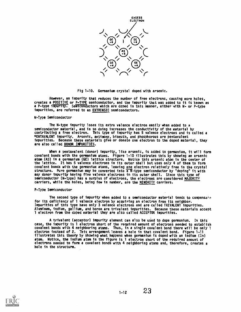
EXCESSELECTRON
Fig 1-10. Germanium crystal doped with arsenic.
However, an impurity that reduces the number of free electrons, causing more holes,creates a POSITIVE or P-TYPE semiconductor, and the impurity that was added to it is known asa P-type iiR071177 SeBTEMuctors which are doped in this manner, either with N- or P-typeimpurities, are referred to as EXTRINSIC semiconductors.
N-Type Semiconductor
The N-type impurity loses its extra valence electron easily when added to asemiconductor material, and in so doing increases the conductivity of the material bycontributing a free electron. This type of impurity has 5 valence electrons and is called a0ENTAVALENT impurity. Arsenic, antimony, bismuth, and phosphorous are pentavalentimpurities. Because these materials give or donate one electron to the doped material, theyare also called DONOR IMPURITIES.
When a pentavalent (donor) impurity, like arsenic, is added to germanium, it will formcovalent bonds with the germanium atoms. Figure 1-10 illustrates this by showing an arsenicatom (AS) in a germanium (GE) lattice structure. Notice this arsenic atom in the center ofthe lattice. It has 5 valence electrons in its outer shell but uses only 4 of them to formcovalent bonds with the germanium atoms, leaving one electron relatively free in the crystalstructure. Pure germanium may be converted into iWtype semiconductor by "doping" it withany donor impurity having five valence electrons in its outer shell. Since this type ofsemiconductor (N-type) has a surplus of electrons, the electrons are considered MAJORITYcarriers, while the holes, being few in number, are the MINORITY carriers.
P-Type Semiconductor
The second type of impurity when added to a semiconductor material tends to compensatefor its deficiency of 1 valence electron by acquiring an electron from its neighbor.Impurities of this type have only 3 valence electrons and are called TRIVALENT impurities.Aluminum, indium, gallium, and boron are trivalent impurities. Because these materials accept1 electron from the doped material they are also called ACCEPTOR impurities.
A trivalent (acceptor) impurity element can also be used to dope germanium. In thiscase, the impurity is 1 electron short of the required amount of electrons needed to establishcovalent bonds with 4 neighboring atoms. Thus, in a single covalent bond there will be only 1electron instead of 2. This arrangement leaves a hole in that covalent bond. Figure 1-11illustrates this theory by showing what happens when germanium is doped with an indium (In)atom. Notice, the indium atom in the figure is 1 electron short of the required amount ofelectrons needed to form a covalent bonds with 4 neighboring atoms and, therefore, creates ahole in the structure.

Fig 1-11. Germanium crystal doped with indium.
Gallium and boron, which are also trivalent impurities, exhibit these samecharacteristics when added to germanium. The holes can only be present in this typesemiconductor when a trivalent impurity is used. Note that a hole carrier is not created bythe removal of an electron from a neutral atom, but is created when a trivalent impurityenters into covalent bonds with a tetravalent (4 valence electrons) crystal structure. Theholes in the type semiconductor (P-type) are considered the MAJORITY carries since they arepresent in the material in the greatest quantity. The electrons, on the other hand, are theMINORITY carries.
EXERCISE: Answer the following questions and check your responses against those listed atthe end of this study unit.
1. Define matter.
2. List the three different states of matter.
a.
b.
C.
3. What is the outer shell of an atom called?
4. State, in terms of energy bands, whether a substance is a good insulator,semiconductor, or conductor.
5. What term is used to describe the definite discrete amounts of energy required tomove an electron from a lower shell to a higher shell?
6. Ilhat is the term used to describe the sharing of valence electrons between two ormore atoms?

7. State the two types of current flow in a semiconductor.
a.
b.
8. What is the name given to a piece of pure semiconductor material that has an equalnumber of electrons and holes?
9. What is the name given to a doped germanium crystal with an excess of free holes?
10. What are the majority of carriers in an N-Type semiconductor?
Work Unit 1-3. SEMICONDUCTOR DIODE
STATE THE PURPOSE OF A PN JUNCTION DIODE.
SPECIFY, IN REFERENCE TO THE SCHEMATIC SYMBOL FOR A DIODE, THE DIRECTION OFELECTRON FLOW.
SPECIFY, IN ORDER TO REVERSE BIAS IN A PN JUNCTION, THE TERMINAL OF A BATTERY THATIS CONNECTED TO THE P MATERIAL.
STATE THE TYPE OF BIAS WHICH OPPOSES THE PN JUNCTION BARRIER.
If we join a section of N-type semiconductor material with a similar section of P-typesemiconductor material, we obtain a device known as a PN JUNCTION. (The area where the N andP regions meet is appropriately called the junction.) Wsual characteristics of thisdevice make it extremely useful in electronics as a diode rectifier. The diode rectifier orPN junction diode performs the same functions as its counterpart in electron tubes but in adifferent way. The diode is nothing more than a two-element semiconductor device that makesuse of the rectifying properties of a PN junction to convert alternating current into directcurrent by permitting current flow in only one direction. The schemati,1 symbol of a PNjunction diode is shown in figure 1-12. The vertical bar represents the cathode (N-typematerial) since it is the source of electrons and the arrow represents thigai (P-typematerial) since it is the destination of the electrons. The label "CR1" is an alphanumericalcode used to identify the diode. In this figure, we have only one drae so it is labeled CRI(crystal rectifier number one). If there were four diodes shown in the diagram then the lastdiode would be labeled CR4. The heavy dark line shows electron flow. Notice it is againstthe arrow. For further clarification, a pictorial diagram for a PN junction and an actualsemiconductor (one of many types) are also illustrated.
CATHODE
CR1 ELECTRONFLOW
ANODE OCHEMATIC1VIEW /
PN JUNCTION
.-{N-TVPEIP-TYPE VIEW
(ACTUAL1VIEW /
Fig 1-12. The PN junction diode.

ACCEPTORIMPURITY PELLET
(A) GROWN INGOT
(B) FUSED SPECIMEN
fgCUT BAR
Fig 1-13. Grown and fused PN junctions from which bars are cut.
Merely pressing together a section of P material and a section of N material, however,is not sufficient to produce a rectifying junction. To form a proper PN junction, thesemiconductor should be in one piece, but divided into a P-type impurity region and an N-typeimpurity region. This can be done in various ways. One way is to mix P-type and N-typeimpurities into a single crystal during the manufacturing process. By so doing, a P-region isgrown over part of a semiconductor's length and an N-region is grown over the other part.This is called a GROWN junction and is illustrated in view (A) of figure 1-13. Another way toproduce a PN junction fs to melt one typical type of impurity into a semiconductor of theopposite type impurity. For example, a pellet of acceptor impurity is placed on a wafer ofN-type germanium and heated. Under controlled temperature conditions, the acceptor impurityfuses into the wafer to form a P-region within it, as shown in view (B) of figure 1-13. Thistype of junction is known as an ALLOY or FUSED-ALLOY junction, and it is one of the mostcommonly used junctions. In figure 1-14, a POINT-CONTACT type of construction is shown. Itconsists of a fine metal wire, called a cat whisker, that makes contact with a small area onthe surface of an N-type semiconductor as shown in view (A) of the figure. The PN union isformed in this process by momentarily applying a high-surge current to the wire and the N-typesemiconductor. The heat generated by this current converts the material nearest the point ofcontact to a P-type material (view B).
CAT WHISKER C:1iL;)CAT WHISKER
1111141?:41(A) (B)
Fig 1-14. The point-contact type of diode construction.
Still another process is to heat a section of semiconductor material to near meltingand then diffuse the impurity atoms into a surface layer. Regardless of the process, theobject is to have a perfect bond everywhere along the uniLa (interface) between the P and Nmaterials. Proper contact along the union is important because, as we will see later, theunion (junction or interface) is the rectifying agent in the diode.
Now that you are familiar with P- and N-type materials, how these materials are joinedtogether to form a diode, and the function of the diode, let us continue our discussion withthe operation of the PN junction. However, before you can understand how the PN junctionworks, we must first consider current flow in the materials that make up the junction and thenwhat happens initially within the junction when these two materials are joined together.
1-15 26

CoNductioN IN the N-type of semiconductor, or crystal, is similar to conduction in acopper wire. That is, with voltage applied across the material electrons will move throughthe crystal jolt as current would flow in a copper wire. This is shown in figure 1-16. Thepositive potential of the battery will attract the free electrons in the crystal. Theseelectrons sill leave the crystal and flow into the positive terminal of the battery. As anelec!ron leaves the crystal, an electron from the negative terminal of the battery will enterthe crystal, thus completing the current path. Therefore, the majority current carries in theN-type notarial (electrons) are repelled by the negative side of the battery and move throughtae crystal toward the positive side of the battery.
N -TYPE MATERIAL
Fig 1-16. Current flow in the N -type material.
Correia flow through the -type notarial is illustrated in figure 1-16. Conduction inthe material is by positive holes, instoad of negative electrons. The hole moves from thepositive terminal of the material to the negative terminal. Electrons from the externalcirceit eeter the rietive tevielaal of the material and fill holes in the vicinity of thisterminal. At VAC positive terminal, electrons are removed from the Covalent bonds, thuscreating new holes. This process continues as the steady stream of holes (hole current) movestoward the moistly* terminal.
P-TYPE MATERIAL
4w-noLa Low-
Cs
Fig 1 -IC Current flow in the P -type material.
Notice in both N-type amd F -type materials, current flow in the external circuitconsists of electrons moving out the negative terminal of the battery and into the positivetermimel of the battery. Nolo flow, on the other hand, only exists within the material itself.
Althsegh the N-type material has an excess of free electrons, its still electrically
Neutral. This is because the donor atoms in the N material were left with positive chargesattar free electrons became available by covalent bonding (the protons outnumbered theelectrons). Therefore, for every free electron in the N material there is a correspondingpositively chareed atom to balaNce it. The end result is that the N material has an overall
cherge of am,
1-1627

By the same reasoning, the P-type material is also electrically neutral because thee xcess of holes in this material is exactly balanced by the number of electrons. Keep in mindthat the holes and electrons are still free to move in the material because they are onlyloosely bound to their parent atoms.
It would seem that if we joined the N and P materials together by one of the processesmentioned earlier that all the holes and electrons would pair up. On the contrary, this doesnut happen. Instead the electrons in the N material diffuse (move or spread out) across thejunction into the P material and fill some of the holes. At the same time the holes in the Pmaterial diffuse across the junction into the N material and are filled by N materiale lectrons. This process is called JUNCTION RECOMBINATION reducing the number of freeelectrons and holes in the vicinity of the junction. Because there is a depletion, or lack offree electrons and holes in this area, it is known as the DEPLETION REGION.
The loss of an electron from the N-type material created a positive ion in the Nmaterial while the loss of a hole from the P material created a negative ion in the material.These ions are fixed in place in the crystal lattice structure and cannot move. Thus, theymake up a layer of fixed charges on the two sides of the junction as shown in figure 1-17. Onthe N side of the junction, there is a layer of positively charged ions; on the P side of thejunction there is a layer of negatively charged ions. An electrostatic field, represented bya small battery in the figure, is established across the junction between the oppositelycharged ions. The diffusion of electrons and holes across the junction will continue untilthe magnitude of the electrostatic field is increased to the point where the electrons andholes no longer have enough energy to overcome it, and are repelled by the negative andpositive ions respectively. At this point equilibrium is established and, for all practicalpurposes, the movement of carriers across the junction cease. For this reason, theelectrostatic field created by the positive and negative ions in the depletion region iscalled a barrier.
The action just described occurs almost instantly when the junction is formed. Onlythe carriers in the immediate vicinity of the jaRTUR7iFe affected. The carriers throughoutthe ireiTair of the N and P material are relatively undisfilfiririd remain in a balancedcondition.
JUNCTION
P 000 le -Notoo -occle e1-
o 000 -
I ; DEPLETION REGION
-"ELECTROSTATM FIELD0 HOLE- FREE ELECTRONe NEGATIVE ION
POSITIVE ION
Fig 1-17. The PN junction barrier formation.
FORWARD BIAS-an external voltage applied to a PN junction is called BIAS. If, forexample, a battery is used to supply bias to a PN junction and is connected so that itsvoltage opposes the junction field, it will reduce the junction barrier and therefore aidcurrent flow through the junction. This type of bias is known as FORWARD BIAS, and it causesthe junction to offer only minimum resistance to the flow of curren .
Forward bias is illustrated in figure 1-18. Notice the positive terminal of the biasbattery is connected to the P-type material and the negative terminal of the battery isconnected to the N-type material. The positive potential repels holes toward the junctionwhere they neutralize some of the negative ions. At the same time, the negative potentialrepels electrons toward the junction where they neutralize some of the positive ions. Sinceions on both sides of the barrier are being neutralized, the width of the barrier decreases.Thus, the effect of the batteny voltage in the forward-bias direction is to reduce the barrierpotential across the junction to allow majority carriers to cross the junction. Current flowin the forward-biased PN junction is relatively simple. An electron leaves the negat veterminal of the battery and moves to the terminal of fhe N-type material. It enters the Nmaterial, where it is the majority carrier, and moves to the edge of the junction barrier.
1-1728

Due to forward bias, the barrier offers less opposition to the electron and it will passthrough the depletion region into the P-type material. The electron loses energy inovercoming the opposition of the junction barrier, and upon entering the P material, combineswith a hole. The hole was produced when an electron was extracted from the P material by thepositive potential of the battery. The created hole moves through the P material toward thejunction where it combines with an electron.
DEPLETION REGION
120000lies!:-000001
--:-----421
HOLES ELECTRONS I
00000165Abl-----va-rwi
.4 le-ORIGINAL BARRIER
ELECTRON FLOW
Fig 1-18. Forward-biased PN junction.
It is important to remember that in the forward biased condition, conduction is byMAJORITY current carriers (holes in the P-type material and electrons in the N-typematerial). Increasing the battery voltage will increase the number of majority carriers
WiTigliFit the junction and will, therefore, increase the current flow. If the batteryvoltage is increased to the point where the barrier is greatly reduced, a heavy current willflow and the junction may be damaged from the resulting heat.
REVERSE BIAS. If the battery mentioned earlier is connected across the junction sothat its voltage aids the junction, it will increase the junction barrier and thereby offer aTrliF resistance to the correct flow through the junction. This type of bias is known as
reverse bias.
-.4 fo-DEPLETION REGION
P000peeel---N0000199,0430---0000' i- --0000M-949W- ---0000;09991--
-0I f- ORIGINAL BARRIER
IN+NO ELECTRON FLOW
Fig 1-19. Reverse biased PN junction.
To reverse bias a junction diode, the negative battery terminal is connected to theP-type material, and the positive battery terminal to the N-type material as shown in figure1-19. The negative potential attracts the holes away from the edge of the junction barrier onthe P side, while the positive potential attracts the electrons away from the edge of thebarrier on the N side. This action increases the barrier width because there are morenegative ions on the P side of the junction, and more positive ions on the N side of the
junction. Notice in the figure the width of the barrier has increased. The increase in thenumber of ions prevents current flow across the junction by majority carriers. However, the
current flow across the barrier is not quite zero because of the minority carriers crossingthe junction. As you recall, when the crystal is subjected to an external source of energy
(light, heat, etc.), electron-hole pairs are generated. The electron-hole pairs produce
minority current carriers. There are minority current carriers in both regions: holes in the
N material and electrons in the P material. With reverse bias, the electrons in the P-typematerial are repelled toward the junction by the negat ve terminal of the battery. As the

electron moves across the junction, it will neutralize a positive ion in the N-type material.Similarly, the holes in the N-type material will be repelled by the positive terminal of thebattery toward the junction. As the hole crosses the junction, it will neutralize a negativeion in the P-type material. This movement of minority carriers is called MINORITY CURRENTFLOW, because the holes and electrons involved come from the electron-hole pairs that aregenerated in the crystal lattice structure, and not from the addition of impurity atoms.
Therefore, when a PN junction is reverse biased, there will be no current flow due tomajority carriers but a very small amount of current due to minority carriers crossing thejunction. However, at normal operating temperatures this small current may be neglected.
In summary, the most important point to remember about the PN.Junction diode is itsability to offer very little resistance to current flow in the forwara-bias direction butmaximum resistance to current flow when reverse biased.
A good way of illustrating this point is by plotting a graph of the applied voltageversus the measured current. Figure 1-20 shows a plot of this voltage-current relationship(characteristic curve) for a typical PN junction diode.
To determine the resistance from the curve in this figure we can use Ohm's law,
R = -. For example at point A the forward-bias voltage is 1 volt and the forward-bias current
is 5 milliamperes. This represents 200 ohms of resistance (1 volt/5 mA 200 ohms). However,at point B the voltage is 3 volts and the current is 500 milliamperes. This results in 60ohms of resistance of the diode. Notice that when the forward-bias voltage was tripled (1volt to 3 volts), the current increased ten times (5mA to 50 mA). At the same time theforward-bias voltage increased, the resistance decreased from 200 ohms to 60 ohms. In otherwords, when forward bias increases, the junction barrier gets smaller and this resistance tocurrent flow decreases.
80v 401,/
50mA
zz00m 30mA4
N6A
10mA
W 2v 3v 41,
5000A FORWARD BIAS
1000
Bow
Fig 1-20. PN junction diode characteristics curve.
On the other hand, the diode conducts very little when reverse biased. Notice atpoint C the reverse bias voltage is 80 volts and the current is only 100 microamperes. Thisresults in 800 k ohms of resistance,-VITFTs considerably larger than the resistance of thejunction with forward bias. Because of these unusual features, the PN junction diode is oftenused to convert alternating current into direct current (rectification).
1-19 30

EXERCISE: Answer the following questions and check your responses against those listed atthe end of this study unit.
1. What is the purpose of a PN junction diode?
2. In reference to the schematic symbol for a diode, do electrons flow toward or awayfrom the arrow?
3. What type of PN diode is formed by using a fine metal wire and a section of N-typesemiconductor material?
4. Conduction in which type of semiconductor material is similar to conduction in acopper wire?
5. What is the name of the area in a PN junction that has a shortage of electrons andholes?
6. In order to reverse bias in a PN junction, what terminal of a battery is connectedto the P terminal?
7. What type of bias opposes the PN junction barrier?
Work Unit 1-4. PN JUNCTION APPLICATION
DEFINE A LOAD AS REFERRED TO IN ELECTRONICS.
SPECIFY THE OUTPUT OF A HALF-WAVE RECTIFIER.
STATE THE TYPE OF BIAS WHICH MAKES A DIODE ACT AS A CLOSED SWITCH.
SPECIFY THE TYPE OF RECTIFIER THAT IS CONSTRUCTED BY SANDWICHING A SECTION OFSEMICONDUCTOR MATERIAL BETWEEN TWO METAL PLATES.
SPECIFY WHAT IS USED TO SHOW HOW DIODE PARAMETERS VARY OVER A FULL OPERATING RANGE.
DEFINE DIODE RATINGS.
Until now, we have mentioned only one application for the diode - rectification, butthere are many more applications that we have not yet discussed. Variations in doping agents,semiconductor materials, and manufacturing techniques have made it possible to produce diodesthat can be used in many different applications. Examples of these types of diodes are:sj nal diodes, rectifying diodes, zener diodes (voltage protection diodes for power supplies),varactors amplifying and switching diodes), and many more. Only applications for two of theWRiTERibnly used diodes, the signal diode and rectifier diode, will be presented in thiswork unit. The other diodes willbe explained later in this course.
One of the most important uses of a diode is rectification. The normal PN junctiondiode is well suited for this purpose as it conducts very heavily when forward biased(low-resistance direction) and only slightly when reverse biased (high-resistance direction).If we place this diode in series with a source of a.c. power, then the diode will be forwardand reverse biased every cycle. Rectification is accomplished in this situation, when thecurrent flows more easily in one direction than the other. The simplest rectifier circuit isa half-wave rectifier (fig 1-21) which consists of a diode, an a. c. power source, and a loadresistor.
1-20 31

T ICR I
ACINPUT
R OUTPUT
T I
''42k;"OUTPUT
ACINPUT
T I T RANSFORMERRI.- LOAD RESISTORCR I - MODE
(A)
CR I
(B)
Fig 1-21. Simple half-wave rectifier.
The transformer (71) in the figure provides the a.c. input to the circuit; the diode(CR1) provides the rectification; and the load resistor (RL) serves two purposes: it limitsthe amount of current flow in the circuit to a safe level, and it also develops thelal5U--signal due to the current flow through it.
Before describing how this circuit operates, the definition of the word "load" as itapplies to power supplies must be understood. Load is defined as any device that drawsvorrent. A device that draws little is considered a light load; whereas, a device-5H drawsa large amount of current is a heavy load. Remember that when we speak of "load," we arespeaking about the device that draws current from the power source. This device may be asimple resistor, or one or more complicated electronic circuits.
During the positive half-cycle of the input signal (solid line) in figure 1-21(A), thetop of the transformer is positive with respect to ground. The dots on the transformerindicate points of the same polarity. With this condition, the diode is forward biased, thedepletion region is narrow, the resistance of the diode is low, and current flows through thecircuit in the direction of the solid lines. When this current flows through the loadresistor, it develops a negative to positive voltage drop across it which appears as apositive voltage at the output terminal.
When the a.c. input goes in a negative direction, the top of the transformer becomesnegative and the diode becomes reverse biased. With reverse bias applied to the diode, thedepletion region increases, the resistance of the diode is high, and minimum current flowsthrough the diode. For all practical purposes, there is no output developed across the loadresistor during the negative alternation of the input signal as indicated by the broken linesin the figure. Although only one cycle of input is shown, it should be realized that theaction described above continually repeats itself, as long as there is an input. Therefore,since only the positive half-cycles appear at the output, then this circuit converted the a.c.input into a positive pulsating d.c. voltage. The frequency of the output voltage is equal tothe frequency of the applied a.c. signal since there is one pulse out for each cycle of thea.c. input. For example, if the input frequency is 60 hertz (60 cycles per second), theoutput frequency is 60 pulses per second (pps).
However, if the diode is reversed as shown in view (B) of figure 1-21, a negativeoutput voltage would be obtained. This is because the current would be flowing from the topof RL toward the bottom, making the output at the top of RL negative in respect to thebottom or ground. Because current flows in this circuit only during half of the input cycle,it is called a half-wave rectifier.
The semiconductor diode shown in the figure can be replaced by a metallic rectifierand still achieve the same results. The metallic rectifier, sometimes referred to as adry-disc rectifier, is a metal-to-semiconductor, large-area,contact device. Its constructionis distinctive; a semiconductor is sandwiched between two metal plates, or electrodes, asshown in figure 1-22. Note in the figure that a barrier, with a resistance many times greaterthan that of the semiconductor material, is constructed on one of the metal electrodes. The
1-21
32
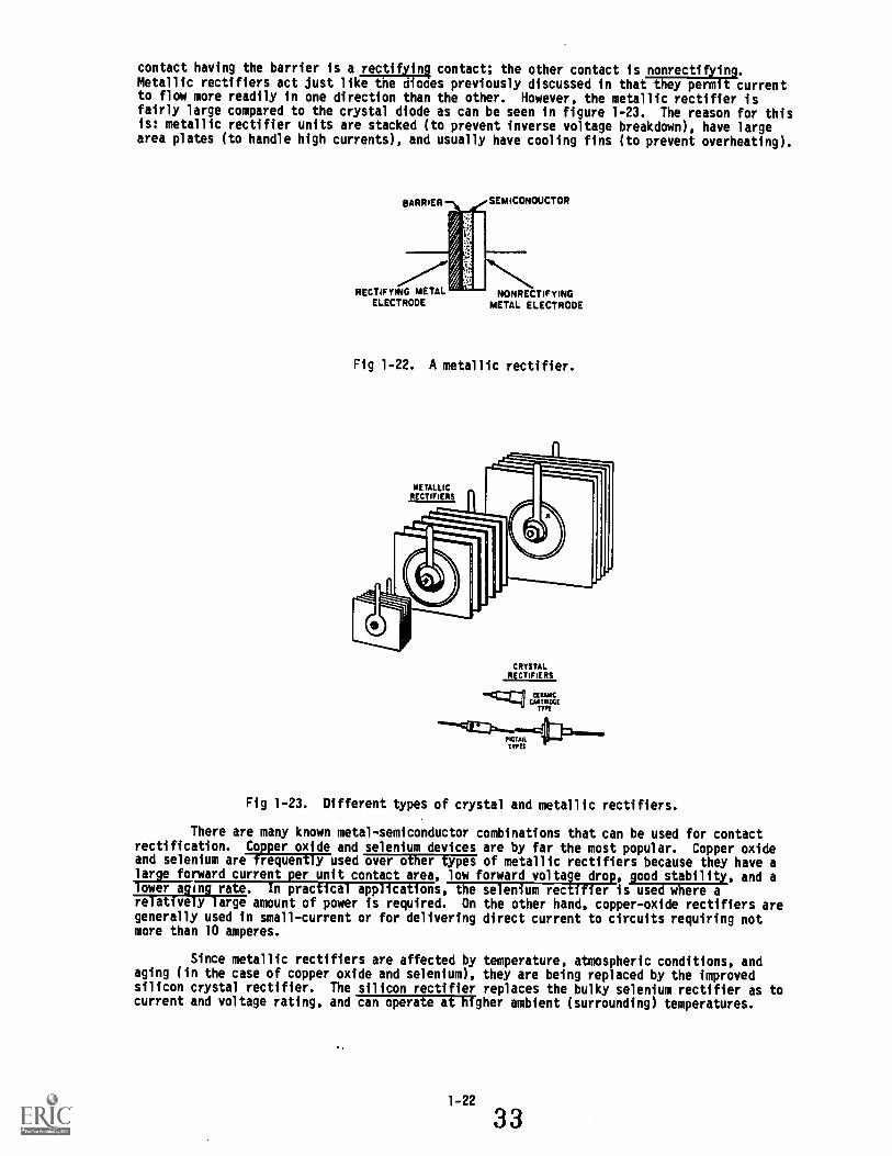
contact having the barrier is a rectif ing contact; the other contact is nonrectifying.Metallic rectifiers act just like tne d odes previously discussed in that they permit currentto flow more readily in one direction than the other. However, the metallic rectifier isfairly large compared to the crystal diode as can be seen in figure 1-23. The reason for thisis: metallic rectifier units are stacked (to prevent inverse voltage breakdown), have largearea plates (to handle high currents), and usually have cooling fins (to prevent overheating).
BARRIER SEMICONOUCTOR
RECTIFYING METALELECTRODE
NONRECTIFYINGMETAL ELECTRODE
Fig 1-22. A metallic rectifier.
METALLICRECTIFIERS
CRYSTALRECTIFIERS
ft.CC:C1 CRAWmama
PIGTAILTYPES
Fig 1-23. Different types of crystal and metallic rectifiers.
There are many known metal-semiconductor combinations that can be used for contactrectification. Copper oxide and selenium devices are by far the most popular. Copper oxideand selenium are frequently used over other types of metallic rectifiers because they have alarge forward current per unit contact area, low forward voltage drop, good stability, and alower aging rate. In practical applications, the selenium rectifier is used where arelatively large amount of power is required. On the other hand, copper-oxide rectifiers aregenerally used in small-current or for delivering direct current to circuits requiring notmore than 10 amperes.
Since metallic rectifiers are affected by temperature, atmospheric conditions, andaging (in the case of copper oxide and selenium), they are being replaced by the improvedsilicon crystal rectifier. The silicon rectifier replaces the bulky selenium rectifier as tocurrent and voltage rating, and can operate at higher ambient (surrounding) temperatures.

OV IN
INPUT+ V IN
1r
CURRENT FLOW
0°.1OV OUT
(CRI CONDUCTING)
OUTPUTCLOSED SW
+V OUTir lERT ECT-OFF)
-/OPEN SW
Fig 1-24. Basic diode switch.
In addition to their use as simple rectifiers, diodes are also used in circuits thatmix signals together (mixers), detect the presence of a signal (detector), and act as a switch"to open or cfose a circuit." Diodes used in these applications are commonly referred to as"signal diodes." The simplest application of a signal diode is the basic diode switch shownin figure 1-24.
When the input to this circuit is at zero potential, the diode is forward biasedbecause of the zero potential on the cathode and the positive voltage on the anode. In thiscondition, the diode conducts and acts as a straight piece of wire because of its very lowforward resistance. In effect, the input is directly coupled to the output resulting in zerovolts across the output terminals. Therefore, the diode acts as a closed switch when itsanode is positive with respect to its cathode.
If we apply a positive input voltage (equal to or greater than the positive voltagesupplied to the anode) to the diode's cathode, the diode will be reverse biased. In thissituation, the diode is cut off and acts as an open switch between the input and outputterminals. Consequently, with no current flow in the circuit, the positive voltage on thediode's anode will be felt at the output terminal. Therefore, the diode acts as an openswitch when it is reverse biased.
Semiconductor diodes have properties that enable them to perform many differentelectronic functions. To do their jobs, engineers and technicians must be supplied with dataon these different types of diodes. The information presented for this purpose is calledDIODE CHARACTERISTICS. These characteristics are supplied by manufacturers either in theirmanuals or on specification sheets (data sheets). Because of the scores of manufacturers andnumerous diode types, it is not practical to put before you a specification sheet and call ittypical. Aside from the differences between manufacturers, a single manufacturer mAy evensupply specification sheets that differ both in format and content. Despite thesedifferences, certain performance and design information is normally required. It is thisinformation that will be discussed in the next few paragraphs.
A standard specification sheet usually has a brief description of the diode. Includedin this description is the type of diode, the major area of apElication, and any s ecialfeatures. Of particular interest is the specific application ror which the diode Is suited.Ternanufacturer also provides a drawing of the diode which gives dimensions, right, and, ifappropriate, any identification marks. In addition to the above diii,--iNi7o1 owinginformation is also provided: a static operating table (giving spot values of parametersunder fixed conditions), sometimes a characteristic curve similar to the one in figure 1-20(showing how parameters vary over the full operating range), and diode ratings (which are thelimiting values of operating conditions outside which could cause diode damage).
Manufacturers specify these various diode operating parameters and characteristicswith "letter symbols" in accordance with fixed definitions. The following is a list, byletterWigol, of the major electrical characteristics for the rectifier and signal diodes.

RECTIFIER DIODES
D.C. BLOCKING VOLTAGE [Vg] - the maximum reverse d.c. voltage which will notcause breakdown.
AVERAGE FORWARD VOLTAGE PROP [Vp(m)] - the average forward voltage drop acrossthe rectifier given at a specified forward current and temperature.
AVERAGE RECTIFIER FORWARD CURRENT (IFIAV)] - the average rectified forwardcurrent at a specified temperature, usually at 60 Hs with a resistive load.
AVERAGE REVERSE CURRENT EIR(AV)] - the average reverse current at a specifiedtemperature, usually at 60 Hz.
PEAK SURGE CURRENT [Isurge] the peak current specified for a given number ofcycles or portion of a cycTe.
SIGNAL DIODES
PEAK REVERSE VOLTAGE [PRY] - the maximum reverse voltage which can be appliedbefore reaching the breakdown point. (PRV also applies to the rectifier diode.)
REVERSE CURRENT [IR) - the small value of direct current that flows when asemiconductor diode has reverse bias.
MAXIMUM FORWARD VOLTAGE DROP AT INDICATED FORWARD CURRENT [Vp@IF] - themaximum forward voltage drop across the diode at the indicated forward current.
REVERSE RECOVERY TIME (trr) - the maximum time taken for the forward-bias diodeto recover its reverse bias.
The electrical characteristics (by letter symbols) for the other types of diodes willappear later in this course.
The ratings of a diode (as stated earlier) are the limiting values of operatingconditions which if exceeded could cause damage to a diode by either voltage breakdown oroverheating. The PN junction diodes are generally rated for: MAXIMUM AVERAGE FORWARDCURRENT, PEAK RECURRENT FORWARD CURRENT, MAXIMUM SURGE CURRENT, and PEAK REVERSE VOLTAGE.
Maximum average forward current is usually given at a specified temperature,usually 260C, (770F) and refers to the maximum amount of average current which can bepermitted to flow in the forward direction. If this rating is exceeded, structure breakdowncan occur.
Peak recurrent forward current is the maximum peak current which can be permittedto flow in the forward direction in tne form of recurring pulses.
Maximum surge current is the maximum current permitted to flow in the forwarddirection in the form of non-recurring pulses. Current should not equal this value for morethan a few milliseconds.
Peak reverse voltape(PRV) is one of the most important ratings. PRV indicates themaximum reverse-bias voltage wnich may be applied to a diode without causing junctionbreakdown.
All of the above ratings are subject to change with temperature variations. If, forexample, the operating temperature is above that stated for the ratings, then the ratings mustbe deereased.
EXERCISE: Answer the following questions and check your responses against those listed atthe end of this study unit.
1. What is a load?
1-24
35

2. What is the output of a half-wave rectifier?
3. What type of bias makes a diode act as a closed switch?
4. What type of rectifier is constructed by sandwiching a section of semiconductormaterial between two metal plates?
5. What is used to show how diode parameters vary over a full operating range?
6. What is meant by diode ratings?
Work Unit 1-5. DIODE IDENTIFICATION AND MAINTENANCE
IDENTIFY THE LETTER "N" AS USED IN THE SEMICONDUCTOR IDENTIFICATION SYSTEM.
NAME THE TYPES OF DIODES BY THE COLOR CODE SYSTEM.
SPECIFY THE GREATEST THREAT TO A DIODE.
STATE WHAT IS INDICATED BY TWO HIGH RESISTANCE MEASUREMENTS WHEN CHECKING A DIODEWITH AN OHMMETER.
There are many types of diodes varying in size from the size of a pinhead (used insubminiature circuitry) to large 250-ampere diodes (used in high power circuits). Because
there are so many different types of diodes, then some system of identification is needed todistinguish one diode from another. This is accomplished with the semiconductoridentification system shown in figure 1-25. This system is not on13715a-57Urodes buttransistors and many other special semiconductor devices as well. As illustrated in thisfigure, the system uses numbers and letters to identify different types of semiconductordevices. The first numarTrihe siiiii-fidicates the number of Junctions in thesemiconductor device and is a number, one less than the number of active elements. Thus 1
designates a diode; 2 designates a transistor (which may be considered as made up of twodiodes); and 3 designates a tetrode (a four-element transistor). The letter "N" following the
first number indicates a semiconductor. The 2- or 3-digit number following the letter "N" isa serialized identification number. If needed, this number may contain a suffix letter afterthe last digit. For example, the suffix letter "M" may be used to describe matcning pairs ofseparate semiconductor devices or the letter "R" may be used to indicate modified versions ofthe device which can be substituted for the basic numbered unit. For example, a semiconductordiode designated as type 1N345A signifies a two-element diode (1) of semiconductor material(N) that is an improved version (A) of type 345.

XNYYY
XN Yr,
COMPONENT IDENTIFICATIONNUMBER
X - NUMBER OF SEMICONDUCTOR JUNCTIONSN -A SEMICONDUCTORYYY- IDENTIFICATION NUMBER (ORDER OR REGISTRATION NUMBER)
ALSO INCLUDES SUFFIX LETTER (IF APPLICABLE ) TO INDICATE
1. MATCHING DEVICES
2. REVERSE POLAF TY3. MODIFICATION
EXAMPLE - IN345A (AN IMPROVED VERSION OF THESEMICONDUCTOR DIODE TYPE 345)
Fig 1-25. Semiconductor identification code.
When working with these different types of diodes, it is also necessary to distinguishone end of the diode from the other (anode from cathode). For this reason, manufacturersgenerally code the cathode end of the diode with a "le, "+", "cath", "color dot or band", orby an unusual shape (raised edge or taper) as shown in figure 1-26. In some cases, standardcolor code bands are placed on the cathode end of the diode. This serves two purposes: (1) itidentifies the cathode end of the diode, and (2) it also serves to identify the diode bynumber.
ANODES CATHODES
Fig 1-26. Semiconductor diode markings.
1-26
37

(2 DIGIT TYPEBLACK BAND)
/ /I I I
3 DIGIT TYPE --attrp---
4 DIGIT TYPE
I I ISUFFIX LETTER()
(IF USED)I I
1ST 2ND 3RD 4144
DIGITS 0
SUFFIX LETTER/2,(BLACK IF NO k..9
LETTER
CLH.OR
0DIGIT
0DIODE
SUFFIXLETTER
BLACK 0 -BROWN I A
RED 2 e
ORANGE 3 C
YELLOW 4 D
GREEN 5 E
BLUE 6 F
VIOLET 7 G
GRAY 9 )4
wmaE 9 J
SILVER - -GOLD - -NONE - -
Fig 1-27. Semiconductor diode color code system.
The standard diode color code system is shown in figure 1-27. Take, for example, a
diode with brown, orange, and white bands at one terminal and figure out its identification
number. With brown being a 11111, orange a "3", and white "9", then the device would be
identified as a type 139 semiconductor diode, or spiFTTCally 1N139.
Keep in mind, whether the diode is a small crystal type or a large power rectifiertype, it is still represented schematically, as explained earlier, by the schematic symbol
shown in figure 1-12.
Diodes are rugged and efficient. They are also expected to be relatively trouble
free. Protective encapsulation processes and special coating techniques have even furtherincreased their life expectancies. In theory, a diode should last indefinitely. However, if
diodes are subjected to current overloads, their junctions will be damaged or even destroyed.In addition, the application of excessively high operating voltages can damage or destroy
junctions through arc-over, or excessive reverse currents. One of the greatest dangers to the
diode is heat. Heat causes more electron-hole pairs to be generated which, in turn, increases---TrfcurrerThrv. This increase in current generates more heat and the cycle repeats itself until
the diode draws excessive current. This action is referred to as THERMAL RUNAWAY and
eventually causes diode destruction. Extreme cajtion should be used when working withequipment containing diodes to ensure that these problems do not occur and cause irreparable
diode damage.
The following is a list of some of the special safety precautions which should be
observed when working with diodes.
Never remove or insert a diode into a circuit with voltage applied.
Never pry diodes to loosen them from their circuits.
Always be careful when soldering to ensure that excessive heat is not applied to
the diode.
1-27
38

When testing a diode, ensure that the test voltage does not exceed the diode'smaximum allowable voltage.
Never put your fingers across a signal diode because the static charge from yourbody could short it out.
Always replace a diode with one of the same type or with a direct replacement.
Ensure a replacement diode is put into a circuit in the correct direfltion.
If a diode has been subjected to excessive voltage or temperature and is suspected ofbeing defective, it can be checked in various ways. The most convenient and quickest way oftesting a diode is with an ohmmeter (figure 1-28). fb make this check, simply disconnect oneof the diode leads from the circuit wiring, and make resistance measurements across the leadsof the diode. The resistance measurements obtained depend upon the test-lead polarity of theohmmeter; therefqre, two measurements must be taken. The first measurement is taken with thetest leads connected to either end of the diode and the second measurement is taken with thetest leads reversed on the diode. The larger resistance value is assumed to be the reverse(back) resistance of the diode, and the smaller resistance (front) value is assumed to be theforward resistance. Measurements can be made for comparison purposes using anotheridentical-type diode, known to be good, as a standard. Two high-value resistance measurementsindicate that the diode is open or has a high forward resistance; two low-value resistancemeasurements indicate that the diode is shorted or has a low reverse resistance. A normal setof measurements will show a high resistance in the reverse direction and a low resistance inthe forward direction. The diode's efficiency is determined by how the forward resistance isas compared with the reverse resistance; that is, it is desirable to have as great a ratio(often known as the front to back ratio or the back to front ratio) as possible between thereverse and forward resist:,ce measurements. However, as a rule of thumb, a small signaldiode will have a ratio o everal hundred to one, while a power rectifier can operatesatisfactorily with a ratio of 10 to 1.
OHMMETER
DIODE
Pi
LEADS
REVERSE CONDITION -HIGH RESISANCE MEASUREMENT
OHMMETER
FORWARD CONDITION -La* RESISTANCE MEASUREMENT
Checking a diode with an ohmmeter.
One thing you sn'ld in mind about the ohmmeter check it is not conclusive.It is still possible f,, .11Jde to check good under this test, but breaks down when replacedin the circuit. The problem is that the meter used to check the diode uses a lower voltagethan that which the diode usually operates at in the circuit. Another important point toremember is that a diode should not be condemned because two ohmmeters give different readings
1-283 9

on the diode. This occurs due to the different internal resistance of the ohmmeters and the
different states of charge on the ohmmeter batteries. Because each ohmmeter sends a different
current through the diode, the two resistance value readings on the meters will not be the
same.
Another way of checking a diode is with the substitution method. In this method, a
good diode is substituted for a questionable diode. This technique should be used only after
you have made voltage and resistance measurements to make certain that there is no circuit
defect that mightliamage the substitution diode. If more than one defective diode is present
in the equipment section where trouble has been localized, this method becomes' cumbersome,
since several diodes may have to be replaced before the trouble is corrected. To determine
which stages failed and which diodes are not defective, all of the removed diodes must be
tested. This can be accomplished by observing whether the equipment operates correctly as
each of the removed diodes is reinserted into the equipment.
In conclusion, the only valid check of a diode is a dynamic electrical test which
determines the diode's forward current (resistance) and reverse current (resistance)
parameters. This test can be accomplished using various crystal diode test sets.
EXERCISE: Answer the following questions and check your responses against those listed at
the end of this study unit.
1. What does the letter "N" indicate in the semiconductor identification system?
2. What type of diode has orange, blue, and gray bands?
3. What is the greatest threat to a diode?
4. When checking a diode with an ohmmeter, what is indicated by two high resistance
measurements?
4 01-29

PERIODIC TABLE OF THE ELEMENTSSIMI WO
wow sma HOM
NONNIVALS
IA'Aiia CI NWT NOM awl Geleimahaniameia a MIMIriaciammenamemanemaiaOC121130110 ermanetaniII
enciamenna innIAINTIUMUI
"yb$901
N.
Dc
02116311300130111,P LT a ao kr.
vt,2ii.
aCTIMUN WKSillv.4/01110 110441., MANN IMI 1:1101.11
In NC T PAU YOR INMPIRETATION 01P SYMMS
41

Table 1-1. Periodic Table of the Elements - Continued
Atomic AtomicSymbol Name Number Weight
Au Actinium 89 1(227)Ag Silver 47 107.868Al Aluminum 13 28.982Am Americium 95 (249)Ar Argon 18 39.95As Arsenic 33 74.922At Astatine 85 (210)Au Gold 79 196.987B Boren 5 10.81Ba Barium 56 137.34Be Beryllium 4 9.012Bi Bismuth 83 208.980Bk Berkelium 97 (247)Br Bromine 35 79.904C Carbon 8 12.011Ca Calcium 20 40.08Cd Cadmium 48 112.40Cs Cerium se 140.12Cf Californium 98 (249)Cl Chlorine 17 35.453Cm Curium 98 (247)Co Cobalt 27 58.933Cr Chromium 24 51.998Cs Cesium 55 132.905Cu Copper 29 83.548Dy Dysprosium 86 162.50Es Einsteinium 99 (254)Er Erbium 88 167.28EV Europium 63 151.98F Fluorine 9 18.998Fe Iron 26 55.847Fm Fermium 100 (257)Fr Francium 87 (229)Ga Gallium 31 69.72Gd Gadolinium 84 157.25Ge Germanium 32 72.59H Hydrogen 1 1.008Ha Hahnium 105 (262)He Helium 2 4.003Hf Hafnium 72 178.49Hg Mercury 80 200.59Ho Holmium 67 164.930I Iodine 53 126.904In Indium 49 114.82Ir Iridium 77 192.2K Potassium 19 39.102Kr Krypton 38 83.80La Lanthanum 57 138.91Li Lithium 3 6.94Lr Lawrencium 103 (256)Lu Lutetium 71 174.97Md Mendelevium 101 (258)Mg Magnesium 12 24.305

Table 1-1. Periodic Table of the Elements - Continued
Symbol NameAtomicNumber
AtomicWeight
Mn Manganese 25 54.938Mo Molybdenum 42 95.94N Nitrogen 7 14.007Na Sodium 11 22.990Nb MK= 41 92.908Nd Neodymium 80 144.24Ne Neon 10 20.18Ni Nickel 28 58.71No Nobelium 102 (256)NP Neptunium 93 (237)0 Oxygen 8 15.999Os Osmium 78 190.2P Phosphorus 15 30.974Pa Protactinium 91 (231)Pb Lead 82 207.2rt Palladium 46 108.4Pm Promethium 81 (147)Po Polonium 84 (210)Pr Praseodymium 59 140.907Pt Platinum 78 195.09Pu Plutonium 94 (242)Ra Radium 88 (220Rb Rubidium 37 85.47Re Rhenium 75 188.2Rf Rutherfordium 104 (261)Rh Rhodium 45. 102.905Rn Radon 88 (222)Ru Ruthenium 44 101.07S Sulfur 18 32.08Sb Antimony 51 121.75So Scandium 21 44.956Se Selenium 34 78.98Si Silicon 14 28.088Sm Samarium 62 150.35Sn Tin 50 118.89Sr Strontium 38 87.82Ta Tantalum 73 180.948Tb Terbtum 65 158.924To Technetium 43 (99)To Tellurium 52 127.80Th Thorium 90 232.038Ti Titanium 22 47.90Tl Thallium 81 204.37Tm Thulium 89 158.934U Uranium 92 238.03V Vanadium 23 50.942W Tungsten 74 183.85Xe Xenon 54 131.30Y Yttrium 39 88.905Yb Ytterbium 70 173.04Zn Zinc 30 85.37Zr Zirconium 40 91.22
1 -32
43

SUMMARY REVIEW
Now that you have completed this study unit, you have learned the history ofsemiconductors, their theory of operation, their purpose, and application, and how to identify
and maintain them. If you had any problems it is highly recommended that you go over this
study unit prior to proceeding.
Answer to Study Unit #1 Exercises
Work Unit 1-1.
1. An electrical device which operates by the movement of electrons within a solid
piece of semiconductor material.2. It is the decrease in a semiconductor resistance as temperature rises.
3. a. Space systemsb. Computersc. Data processing equipment
4. The electron tube requires filament or heater voltage; whereas, the semiconductor
device does not. Consequently, no power input is spent by the semiconductor for
conduction.
Work Unit 1-2.
1. Anything that occupies space and has weight
2. a. Solid
b. Liquidc. Gas
3. The valence shell4. The width of the forbidden band5. Quanta6. Covalent bonding7. a. Electron flow
b. Hole flow8. Intrinsic9. P-type crystal
10. Electrons
Work Unit 1-3.
1. To convert alternating current into direct current
2. Toward the arrow
3. Point contact4. N-type material5. Depletion region6. Negative terminal
7. Forward
Work Unit 1-4.
1. Any device that draws current
2. A pulsating d.c. voltage3. Forward bias4. Metallic rectifier5. A characteristic curve6. They are the limiting values of operating conditions outside which operations
could cause diode damage.
Work Unit 1-5.
1. A semiconductor
2. 1N3683. Heat4. That the diode is open or has a high forward resistance
1-33
, 4 4

STUDY UNIT 2
TRANSISTORS
STUDY UNIT OBJECTIVE: WITHOUT THE AID OF REFERENCES, YOU WILL IDENTIFY THEVARIOUS TYPES OF TRANSISTORS AND THEIR CONSTRUCTION, ALPHANUMERICAL DESIGNATIONS,SYMBOLS, AND OPERATION. YOU WILL IDENTIFY THE PRECAUTIONS THAT MUST BE TAKEN WHENWORKING WITH TRANSISTORS. YOU WILL IDENTIFY INTEGRATED CIRCUITS, THEIRCONSTRUCTION, AND ADVANTAGES THEY AFFORD THEIR USERS. LASTLY, YOU WILL IDENTIFYTHE FUNCTION OF MODULAR CIRCUITRY.
The discovery of the first transistor in 1948 by a team of physicists at the BellTelephone Laboratories sparked an interest in solid-state research that spread rapidly. Thetransistor, which began as a simple laboratory oddity, was rapidly developed into asemiconductor device of major importance. The transistor demonstrated for the first time inhistory that amplification in solids was possible. Prior to the transistor, amplification wasachieved only with electron tubes. Transistors now perform numerous electronic tasks with newand improved transistor designs being continually put on the market. In many cases,transistors are more desirable than tubes because they are small, rugged, require no filamentpower, and operate at low voltages with comparatively high efficiency. The development of afamily of transistors has even made possible the miniaturization of electronic circuits.Figure 2-1 shows a sample of the many different types of transistors you may encounter whenworking with electronic equipment.
Transistors have infiltrated virually every area of science and industry, from thefamily car to satellites. The military depends heavily on transistors. The ever increasinguses for transistors have created an urgent need for sound and basic information regardingtheir operation.
From your study of the PN-junction diode in the preceding topic, you now have thebasic knowledge to grasp the principles of transistor operation. In this topic you will firstbecome acquainted with the basic types of transistors, their construction, and their theory ofoperation. You will also find out just how and why transistors amplify. Once this basicinformation is understood, transistor terminology, capabilities, limitations, andidentification will be discussed. Last, we will talk about transistor maintenance, integratedcircuits, boards, and modular circuitry.
Fig 2-1. An assortment of different types of transistors.
Work Unit 2-1. TRANSISTOR FUNDAMENTALS
SPECIFY THE SEMICONDUCTOR DEVICE THAT HAS THREE OR MORE ELEMENTS.
STATE THE ELECTRONIC FUNCIION WHICH MAKES THE TRANSISTOR SPECIAL.

NAME THE VERY FIRST TRANSISTOR.
SPECIFY ONE OF THE MOST IMPORTANT PARTS OF ANY TRANSISTOR MANUFACTURING PROCESS.
The first solid-state device discussed was the two-element semiconductor diode. Thenext device on our list is even more unique. It not only has one more element than the diodebut it can amplify as well. Semiconductor devices that have three or more elements are calledTRANSISTORS. The term transistor was derived from the words TRANSfer and resISTOR. This termrarf104757 because it best describes the operation of the trillintorthe triliiTer of aninput signal current from a low-resistance circuit to a high-resistance circuit. Basic tlly,the transistor is a solid-state device that amplifies by controlling the flow of currentcarriers through its semiconductor materials.
There are many different types of transistors, but their basic theory of operation isall the same. As a matter of fact, the theory we will be using to explain the operation of atransistor is the same theory used earlier with the PN-junction diode except that now two suchjunctions are required to form the three elements of a transistor. The three elements of thetwo junction transistor are: (1) the EMITTER, which gives off, or "emits," current carriers(electrons or holes); (2) the BASE, whiarialrols the flow of current carrier; and (3) theCOLLECTOR, which collects the current carriers.
Transistors are classified as either NPN or PNP according to the arrangement of theirN and P materials. Their basic construction Wacheiral treatment is implied by their names,"NPN" or NPNP." That is, an NPN transistor is formed by introducing a thin region of P-typematerial between two regions of N-type material. On the other hand, a PNP transistor isformed by introducing a thin region of N-type material between two regions of P-typematerial. Transistors constructed in this manner have two PN junctions, as shown in figure2-2. One PN junction is between the emitter and the base; the other PN junction is betweenthe collector and the base. The two junctions share one section of semiconductor material sothat the transistor actually consists of three elements.
PN
JUNCTIONS
EMITTER IN P N
RASE
EMITTER
NPN TYPE
PN
JUNCTIONS
COLLECTOR
P N P ICOLLECTOR
BASE
PNP TYPE
Fig 2-2. Transistor block diagrams.
Since the majority and minority current carriers are different for N and P materials,it stands to reason that the internal operation of the NPN and PNP transistors will also bedifferent. The theory of operation of the NPN and PNP transistors will be discussedseparately in the next few paragraphs. Any additional information about the PN junction willbe given as the theory of transistor operation is developed.
In order to prepare you for the forthcoming information, the two basic types oftransistors along with their circuit symbols are shown in figure 2-4. It should be noted thatthe two symbols are different. The horizontal line represents the base, the angular line withthe arrow on it represents the collector. The direction of the arrow (Fig 2-3) on the emitterdistinguishes the NPN from the PNP transistor. If the arrow points in, (Points iN) thetransistor is a PNP. On the other hand, if the arrow points out, the transistor Ts an NPN(Not Pointing 1NT7-
2-2 46

PNP NPN\ dP""POINTS IN" "NZ POINTING IN"
Fig 2-3. Distinguishing the NPN from the PNP transistor.
Another point you should keep in mind is that the arrow always points into thedirection of hole flow, or from the P to N sections, no matter whether the P section is theemitter or bairlrite other hand, electron flow is always toward or against the arrow, justlike in the junction diode. The very flrst transistors were known as point-contacttransistors. Their construction is similar to the construction of the point-contact diode
covered in study unit 1. The difference, of course, is that the point-contact transistor hastwo P or N regions formed instead of one. Each of the two regions constitutes an electrode
(element) of the transistor. One is named the emitter and the other is named the collector,as shown in figure 2-5, view (A).
EMITTER
EMITTER
COLLECTOR (A)
COLLECTOR
EMITTER
(NPN
B)
COLLECTOR
EMITTER COLLECTOR
(C)
(A)
0PNP
3)
(C)
Fig 2-4. Transistor representations.
Point-contact transistors are now practically obsolete. They have been replaced by
junction transistors, which are superior to point-contact transistors in nearly allresiWal. The junction transistor generates less noise, handles more power, provides highercurrent and voltage gains, and can be mass-produced more cheaply than the point-contacttransistor. Junction transistors are manufactured in much the same manner as the PN-junction
2-3
47

diode discussed earlier. However, when the PNP or NPN material is grown (view B), theimpurity mixing process must be reversed twice in order to obtain the two junctions requiredin a transistor. Likewise, when the alloy-junction (view C) or the diffused-junction (view D)process is used, two junctions must also be created within the crystal.
POINT CONTACT
A
EMITTER COLLEC TOR
BASECOLLECTOR
ALLOY
OR
FUSED JUNC TION
IC)
CHF TUSE0 JUNCTION
(D)
BASE
COLLECTOR
EMI T IT R
C01.1. ECTOR
EMI T TER
Fig 2-5. Transistor constructions.
Although there are numerous ways to manufacture transistors, one of the most importantparts of any manufacturing process is quality control. Without good quality control, manytransistors would prove unreliable because the construction and processing of a transistorgovern its thermal ratings, stability, and electrical characteristics. Even though there aremany variations in the transistor manufacturing processes, certain structural techniques,which yield good reliability and long life, are common to all processes: (1) Wire leads areconnected to each semiconductor electrode; (2) the crystal is specially mounted to protect itagainst mechanical damage; and (3) the unit is sealed to prevent harmful contamination of thecrystal.
EXERCISE: Answer the following questions and check your responses against those listed atthe end of this study unit.
1. Specify the name given to the semiconductor device that has three or more elements.
2. State the electronic function which makes the transistor special?
3. Name the very first transistor.
4. Specify one of thP most important parts of any transistor manufacturing process.
Work Unit 2-2. TRANSISTOR THEORY
SPECIFY WHAT POLARITY VOLTAGE IS APPLIED TO THE COLLECTOR, AND ITS RELATIONSHIP TOTHE BASE VOLTAGE TO PROPERLY BIAS AN NPN TRANSISTOR.
2-4
48

STATE THE PERCENTAGE OF CURRENT IN AN NPN TRANSISTOR THAT REACHES THE COLLECTOR.
STATE THE RELATIONSHIP BETWEEN THE POLARITY OF THE VOLTAGE APPLIED TO THE PNPTRANSISTOR AND THE RELATIONSH:P APPLIED TO THE NPN TRANSISTOR.
NAME THE TWO CURRENT LOOPS IN A TRANSISTOR.
NAME THE LETTER DESIGNATION FOR BASE CURRENT.
You should recall from an earlier discusion that a forward-biased PN junction iscomparable to a low-resistance circuit element because it passes a high current for a givenvoltage. In turn, a reverse-biased PN junction is comparkble to a high-resistance circuitelement. By using the Ohm's law formula for' power (P I'll) and assuming current is heldconstant, you can conclude that the power developed across a high resistance is greater thanthat developed across a low resistance. Thus, if a crystal was to contain two PN junctions(one forward-biased and the other reverse-biased), a low-power signal could be injected intothe forward-biased junction and produce a high-power signal at the reverse-biased junction.In this manner, a power gain would be obtained across the crystal. This concept, which ismerely an extension of the material covered in study unit 1, is the basic theory behind howthe transistor amplifies. With this information fresh in your mind, let's proceed directly tothe NPN transistor.
Just as in the case of the PN junction diode, the N material comprising the two endsections of the NPN transistor contains a number of free electrons, while the center P sectioncontains an excess number of holes. The action at each junction between these sections is thesame as that previously described for the diode. That is, depletion regions develop and thejunction barrier appears. In order to use the transistor as an amplifier, each of thesejunctions must be modified by some external bias voltage. For the transistor to function inthis capacity, the first PN junction (emitter-base junction) is biased in the forward, orlow-resistance, direction. At that same time the second PN junction (base-collector junction)is biased in the reverse, or high-resistance, direction. A simple way to remember how toproperly bias a transistor is to observe the NPN or PNP elements that make up the transistor.The letters of these elements indicate what polarity voltage to use for correct bias. Forinstance, notice the NPN transistor below: shown in figure 2-6.
iCOLLECTOR
BASE
r - - - - -3 EMITTERt i
NI FORWARD-BIAS j
1 71-.Fig 2-6. NPN Transistor.
a. The emitter, which is the first letter in the NPN sequence, is connected to thenegative side of the battery while the base, which is the second letter (NPN), is connected tothe Rositive side.
b. However, since the second PN junction is required to be reverse biased for propertransistor operation, then the collector must be connected to an opposite polarity voltage(positive) than that indicated WMTitter designation (NPN). The voltage on the collectormust also be more positive than the base, shown in figure 2-7.
2-5
49

COLLECTOR r-
tonA.P2
LRCMS BIAS
Fig 2-7 Properly biased NPN transistor.
We now have a properly biased NPN transistor.
In summary, the base of the NPN transistor must be positive with respect to theemitter, and the collector must be more positive than the base.
NPN FORWARD-BIASED JUNCTION (Fig 2-8).--An important point to bring out at this time,which was not mentioned during the explanation of the diode, is the fact that the N materialon one side of the forward-biased junction is more heavily doped than the P material. Thisresults in more current being carried across the junction by the majority carrier electronsfrom the N material than the majority carrier holes from the P material. Therefore,conduction through the forward-biased junction, as shown in figure 2-8, is mainly by majoritycarrier electrons from the N material (emitter).
COLLECTOR
BASE
P FORWARO-BMSE0EMITTER 11111. JUNCTION
0----.ELECTRON FLOW
4/- ----HOLE FLOW
Fig 2-8. The forward-biased junction in an NPN transistor.
With the emitter-to-base junction in the figure biased in the forward direction,electrons leave the negative terminal of the battery and enter the N material (emitter).Since electrons are majority current carriers in the N material, they pass easily through theemitter, cross over the junction, and combine with holes in the P material (base). For eachelectron that fills a hole in the P material, another electron will leave the P material(creating a new hole) and enter the positive terminal of the battery.
2-6

REVERSE CURRENT(MINORITY CURRENT 1
REVERSE- BIASEDJUNCTION
Fig 2-9. The reverse-biased junction in an NPN transistor.
NPN REVERSE-BIASED JUNCTION. (Fig 2-9)--The second PN junction (base-to-collector), orreverse-biased junction as it is called (figure 2-9), blocks the majority current carriersfrom crossing the junction. However, there is a very small current, mentioned earlier, thatdoes pass through this junction. This current is called minority current, or reversecurrent. As you recall, this current was produced by the electron-hole pairs:--Triffinoritycarr ors for the reverse-biased PN junction are the electrons in the P material and the holesin the N material. These minority carriers actualli7EREEI-the current for thereverse-biased junction when electrons from the P material enter the N material, and the holesfrom the N material enter the P material. However, the minority current electrons (as youwill see later) play the most tmportant part in the operation of the NPN transistor.
At this point you may wonder why the second PN junction (base-to-collector) is notforward biased like the first PN junction (emitter-to-base). If both junctions were forwardbiased, the electrons would have a tendency to flow from each end section of the N P Ntransistor (emitter and collector) to the center P section (base). In essence, A:Wild havetwo junction diodes possessing a common base, thus eliminatfiriny amplification and defeatingthe purpose of the transistor. A word of caution is in order at this time. If you shouldmistakenly bias the second PN junction in the forward direction, the excessive current coulddevelop enough heat to destroy the junctions, making the transistor useless. Therefore, besure your bias voltage polarities are correct before making any electrical connections.
NPN JUNCTION INTERACTION (Fig 2-10)-We are now ready to see what happens when we placethe two junctions of the NPN transistor in operation at the same time. For a betterunderstanding of just how the two junctions work together, refer to figure 2-10 during thediscussion.
The bias batteries in this figure have been labeled VCE for the collector voltagesupply, and Vim for the base voltage supply. Also notice the base supply battery is quitesmall, as indicated by the number of cells in the battery, usually 1 volt or less. However,the collector supply is generally much higher than the base supply (normally around 6 volts).As you will see later, this difference in supply voltages is necessary in order to havecurrent flow from the emitter to the collector.
As statid earlier, the current flow in the external circuit is always due to themovement of free electrons. Therefore, electrons flow from the negative terminals of thesupply batteries to the N-type emitter. This combined movement of electrons is known asemitter current (IE). Since electrons are the majority carriers in the N material, theyWiTrEoWEifrlough the if material emitter to the emitter-base junction. With this junctionforward biased, lectrons continue on into the base region. Once the electrons are in thebase, which is a P-type material, they now become minority carriers. Some of the electronsthat move into the base recombine witn available holes. For each electron that recombines,another electron moves out through the base lead as base current III (creating a new hole foreventual combination) and returns to the base supply battery Vim. The electrons that arecombind are lost as far as the collector is concerned. Therefore, in order to make thetransistor more efficient, the base region is made very thin and lightly doped. This reducesthe opportunityfor an electron to recombine with a hole and be lost. Thus, most of the
2-7
51

V98
COLLECTOR
N IREVERSE -BIASED
BASE JUNCTIONIt77-4.N FORWARD-
EMITTER.JUNCTIONMASED
vcc
ELECTRON FLOW0.- HOLE FLOW
Fig 2-10. NPN transistor operation.
electrons that move into the base region come under the influence of the large collectorreverse bias. This bias acts as forward bias for the minority carriers (electrons) in thebase and, as such, accelerates them through the base-collectcr junction and on into thecollector region. Since the collector is made of an N-type material, the electrons that reachthe collector again become majority current carriers. Once in the collector, the electronsmove easily through the N material and return to the positive terminal of the collector supplybattery Vcc as collector current (1c). To further improve on the efficiency of thetransistor, the collector ts made physically larger than the base for two reasons: (1) toincrease the chance of collecting carriers that diffuse to the side as well as directly acrossthe base region, and (2) to enable the collector to handle more heat without damage. Insummary, total current flow in the NPN transistor is through the emitter lead. Therefore, interms of percentage, IE is 100 percent. On the other hand, since the base is very thin andlightly doped, a smaller percentage of the total current (emitter current) will flow in thebase circuit than in the collector circuit. Usually no more than 2 to 5 percent of the totalcurrent is base current (I& while the remaining 95 to 98 percent is collector current(lc) A very basic relationship exists between these two currents:
IE IB + IC
In simple terms this means that the emitter current is separated into base and collectorcurrent. Since the amount of co.rent leaving the emitter is solely a function of theemitter-base bias, and because the collector receives most of this current, a small change inemitter-base bias will have a far greater effect on the magnitude of collector current than itwill have on base current. In conclusion, the relatively small emitter-base bias controls therelatively large emitter-to-collector current.
The PNP transistor works essentially the same as the NPN transistor. However, sincethe emitter, base, and collector it the PNP transistor are made of materials that aredifferent from those used in the NPN transistor, different current carries flow in the PNPunit. The majority current carriers in the PNP transistor are holes. This is in contrast tothe NPN transistor where the majority current carriers are electrons. In order to supportthis different type of current (hole flow), the bias batteries are reversed for the PNPtransistor. A typical bias setup for the PNP transistor is shown in figure 2-11. Notice thatthe procedure used earlier to properly bias the NPN transistor also applies here to the PNPtransistor. The first letter (P) in the PNP sequence indicates the polarity of the voltagerequired for the emitter (positive), and Ihe second letter (N) indicates the polarity of thebase voltage (negative). Since the base-collector junction is always reverse biased, then theopposite polarity voltage (negative) must be used for the collector. Thus, the base of thePhD, transistor must be negative with respect to the emitter, and the collector must be more
2-8
52

negative than the base. Remember, just as in the case of the NPN transistor, this differencein supply voltage is necessary in order to have current flow (hole flow in the case of the PNPtransistor) from the emitter to the collector. Although hole flow is the predominant type ofcurrent flow in the PNP transistor, hole flow only takes place within the transistor itself,while electrons flow in the external circuit. However, it is the internal hole flow thatleads to electron flow in the external wires connected to the transistor.
II
+
FORWARD BIAS j
COLLECTOR
+ IBASE
REVERS BIAS j
EMIT TER
Fig 2-11. A properly biased PNP transistor.
PNP FORWARD-BIASES JUNCTION (Fig 2-12)-Now let's consider what happens when theemitter-base junction in figure 2-12 is forward biased. With the bias setup shown, thepositive terminal of the battery repels the emitter holes toward the base, while the negativeterminal drives the base electrons toward the emitter. When an emitter hole and a baseelectron meet, they combine. For each electron that combines with a hole, another electronleaves the negative terminal of the battery, and enters the base. At the same time, anelectron leaves the emitter, creating a new hole, and enters the positive terminal of thebattery. This movement of electrons into the base and out of the emitter constitutes basecurrent flow (43), and the path these electrons take is referred to as the emitter-basecircuit.
0111
COL LECTOR
BASE
EMI T TER
P
FORWARO MDJUNCTION
49-- ELECTRON FLOW416.-- HOLE FLOW
Fig 2-12. The forward-biased junction in a PNP transistor.
2-9 53

PNP REVERSE-BIASED JUNCTION (Fig 2-13)--In the reverse-biased junction (figure 2-13),the negative voltage on the collector and the positive voltage on the base block the ma oritcurrent carriers from crossing the junction. However, this same negative collector voltageacts as forward bias for the minority current holes in the base, which cross the junction andenter the collector. The minority current electrons in the collector also sense forwardbias--the positive base voltage--and move into the base. The holes in the collector arefilled by electrons that flow from the negative terminal of the battery. At the same time theelectrons leave the negative terminal of the battery, other electrons in the base break theircovalent bonds and enter the positive terminal of the battery. Although there is allyminority current flow in the reverse-biased junction, it is still very small due to thelimited number of minority current carriers.
PNP JUNCTION INTERACTION.--The interaction between the forward - and reverse-biasedjunctions Tn a PNP transistor is very similar to that in an NPN transistor, except that in thePNP transistor, the majority current carriers are holes. In the PNP transistor, shown infigure 2-14, the positive voltage on the emitter repels the holes toward the base. Once inthe base, the holes combine with base electrons, but again, remember that the base region ismade very thin to prevent the recombination of holes with electrons. Therefore, well over 90percent of the holes that enter the base become attracted to the large negative collectorvoltage and pass right through the base. However, for each electron and hole that combine in
REVERSE CURRENT(MINORITY CURRENT)
REVERSE-BIASEDJUNCTION
Fig 2-13. The reversed-biased junction in a PNP transistor.
the base region, another electron leaves the negative terminal of the base battery (Vim) andenters the base as base current (Ig). At the same time an electron leaves the negativeterminal of the battery, another electron leaves the emitter as IE (creating a new hole) andenters the positive terminal of Vgg. Meanwhile, in the collector circuit, electrons fromthe collector battery (Vcc) enter the collector as IC and combine with the excess holesfrom the base. For each hole that is neutralized in the collector by an electron, anotherelectron leaves the emitter and starts its way back to the positive terminal of V.
54
2-10

CLECT*ON #LOW-- #1.0w
Fig 2-14. Pell transistor operation.
Although current flow in the external circuit of the PNP transistor is opposite indirection te that of the NPN transistor, the majority carriers always flow from the emitter tothe collector. This flow of majority carriers also results in the formation of two individualcermet loops within each transistor. One loop is the base-current path and the other loopthe colIector-arraft path. The combination of the current in both of these loops (IN +lE) milts in total transistor current (IE). The most important thing to remember aboutthe toe different t)pes of transistors is that the emitter-base voltage of the PNP transistorhas the some controlling effect on collector current as that of the NPN transistor. In simpleterms, increasing the forward-bias voltage of a transistor reduces the emitter-base junctionbarrier. This action allows mere carriers to reach the collector causing an increase incurrent flow from the emitter to the collector and through the external circuit. Conversely,decrease in the ferwerd-bias voltage reduces collo:tor current.
EXERCISE: Answer the following questions and check your responses against those listed atthe end of this study unit.
1. To properly bis an NPN transistor, what polarity voltage is applied to thecollector?
2. Referring to question 01, what is its relationship to the base voltage?
3. My is conduction through the forward-biased Junction of an NPN transistorprimarily in on. 4irection (namely from the emitter to base)?
4. In the NPN transistor, what section is made very thin compared with the other twosections?
2-11
55

5. What percentage of current In an NPN transistor reaches the collector?
6. What are the majority current carriers in a PNP transistor?
7. What is the relationship between the polarity of the voltage applied to the PNPtransistor and that applied to the NPN transistor?
8. What is the letter designation for base current?
9. Name the two current loops in a transistor.
Work Unit 2-3. BASIC TRANSISTOR AMPLIFIER
NAME THE DEVICE THAT PROVIDES AN INCREASE IN CURRENT, VOLTAGE, OR POWER OF ASIGNAL WITHOUT APPRECIABLY ALTERING THE ORIGINAL SIGNAL.
BESIDES ELIMINATING THE EMITTER-BASE BATTERY, SPECIFY THE OTHER ADVANTAGES THATDIFFERENT BIASING METHODS OFFER.
STATE THE PRIMARY DIFFERENCE BETWEEN THE NPN AND PNP AMPLIFIERS.
IDENTIFY THE MOST UNSTABLE BIASING METHOD.
SPECIFY THE MOST WIDELY USED COMBINATION-BIAS SYSTEM.
SPECIFY THE AMPLIFIER CLASS OF OPERATION THAT ALLOWS COLLECTOR CURRENT TO FLOWDURING THE COMPLETE CYCLE OF THE INPUT.
LIST TWO PRIMARY ITEMS THAT DETERMINE THE CLASS OPERATION OF AN AMPLIFIER.
In the preceding pages we explained the internal workings of the transistor andintroduced new terms, such as emitter, base, and collector. Since you should be familiar bynow with all of these new terms and with the internal operation of the transistor, we willmove on to the basic transistor amplifier.
To understand the overall operation of the transistor amplifier, you must onlyconsider the current in and out of the transistor and through the various components in thecircuit. Therefore, from this point on, only the schematic symbol for the transistor will beused in the illustrations, and rather than thinking about majority and minority carriers, wewill now start thinking in terms of emitter, base, and collector current.
Before going into the basic transistor amplifier, there are two terms you should befamiliar with: AMPLIFICATION and AMPLIFIER. Amplification is the process of increasing thestrength of a SIGNAL. A signal is a general term used to refer to any particular current,voltage, or power in a circuit. An amplifier is the device that provides amplification (theincrease in current, voltage, or power of a signal) WITEUT appreciably altering the originalsignal.
Transistors are frequently used as amplifiers. Some transistor circuits are CURRENTam lifiers, with a small load resistance; other circuits are designed for VOLTAGEamp i cation and have a high load resistance; others amplify POWER.
Now take a look at the NPN version of the basic transistor amplifier in figure 2-15and let's see just how it works.

So far in this discussion, a separate battery has been used to provide the necessaryforward-bias voltage. Although a separate battery has been used in the past for convenience,it is not practical to use a battery for emitter-base bias. For instance, it would take abattery slightly over .2 volts to properly forward bias a germanium transistor while a similarsilicon transistor would require a voltage slightly over .6 volts. However, common batteriesdo not have such voltage values. Also, since bias voltages are quite critical and must beheld within a few tenths of one volt, it is easier to work with bias currents flowing throughresistors of high ohmic values than with batteries.
+MVomV-mV
00Put
(NPN)
OUTPUT
Fig 2-15. The basic transistor amplifier.
By inserting one or more resistors in a circuit, different methods of biasing may beachieved and the emitter-base battery eliminated. In addition to eliminating the battery,some of these biasing methods compensate for slight variations in transistor characteristicsand changes in transistor conduction resulting from temperature irregularities. Notice infigure 2-15 that the emitter-base battery has been eliminated and the bias resistor RB hasbeen inserted between the collector and the base. Resistor REi provides the necessaryforward bias for the emitter-base junction. Current flows in the emitter-base bias circuitfrom ground to the emitter, out the base lead, and through RB to V. Since the currentin the base circuit is very small (a few hundred microamperes) and the forward resistance ofthe transistor is low, only a few tenths of a volt of positive bias will be felt on the baseof the transistor. However, this is enough voltage on the base, along with ground on theemitter and the large positive voltage on the collector, to properly bias the transistor.
With Ql properly biased, direct current flows continuously, with or without an inputsignal throughout the entire circuit. The direct current flowing through the circuit developsmore than just base bias; it also develops the collector voltale (Vc) as it flows through Q1and R. Notice the collector voltage on the output graph. 54Ace it is presented into thecircuit without an input signal, then the output signal starts at the Vc level and eitherincreases or decreases. These d.c. voltages and currents that exist in the circuit prior tothe application of signal are known as QUIESCENT voltages and currents (the quiescent state ofthe circuit).
Resistor RL, the collector load resistor, is placed in the circuit to keep the fulleffect of the collector supply voltage off the collector. This permits the collector voltage(Vc) to change with an input signal, which in turn allows the transistor to amplifyvoltage. Without RL in the circuit, the voltage on the collector would always be equal to
VCC.
The coupling capacitor (Cc) is another new addition to the transistor circuit. Itis used to pass the a.c. input signal and block the d.c. voltage from the preceding circuit.This prevents d.c. in the circuitry on the left of the coupling capacitor from affecting thebias on Ql. The coupling capacitor also blocks the bias of Ql from reaching the input signalsource.
2-13 57

The input to the amplifier is a sine wave that varies a few millivolts above and belowzero. It is introduced into the circuit by the coupling capacitor and is applied between thebase and emitter. As the input signal goes positive, the voltage across the emitter-basejunction becomes more positive. This, in effect, increases forward bias which causes basecurrent to increase at the same rate as that of the input sine wave. Emitter and collectorcurrents also increase but much more than the base current. With an increase in collectorcurrent, more voltage is developed across RL. Since the voltage across RL and the voltageacross Q1 (collector to emitter) must add up to Vcc, an increase in voltage across RLresults in an equal decrease in voltage across Ql. Therefore, the output voltage from theamplifier, taken at the collector of Q1 with respect to the emitter, is a negative alternationof voltage that is larger than the input but has the same sine wave characii7liTTES.
During the negative alternation of the input, the input signal opposes the forwardbias. This action decreases base current which results in a decrease in both emitter andcollector currents. The decrease in current through RL decreases its voltage drop andcauses the voltage across the transistor to rise along with the output voltage. Therefore,the output for the negative alternation of the input is a positive alternation of voltage thatis,larger than the input but has the same sine wave characii7lillTs. By examining both inputand output signals for one complete alternation of the input, we can see that the output ofthe amplifier is an exact reproduction of the input except for the reversal in polarity andthe increased amplitude (a few millivolts as compared to a few volts).
The PNP version of this amplifier is shown in the upper right-hand corner of thefigure 2-15. The primary difference between the NPN and PNP amplifier is the polarity of thesource voltage. With a negative Vcc, the PNP base voltage is slightly negative with respectto ground, which provides the necessary forward bias condition between the emitter and base.
When the PNP input signal goes positive, it opposes the forward bias of thetransistor. This action cancels some of the negative voltage across the emitter-base junctionwhich reduces the current through the transistor. Therefore, the voltage across the loadresistor decreases, and the voltage across the transistor increases. Since Vcc is negative,the voltage on the collector (Vc) goes in a negative direction (as shown on the outputgraph) toward - Vcc (For example, from -5 volts to - 7 volts). Thus, the output is anegative alternation of voltage that varies at the same rate as the sine wave input but isopposite in polarity and has a much larger amplitude. During the negative alternation of theinput signal, the transistor current increases because the input voltage aids the forwardbias. Therefore, the voltage across RL increases, and consequently, the voltage across thetransistor decreases or goes in a positive direction (For example: from - 5 volts to - 3
volts). This action results in a positive output voltage which has the same characteristicsas the input except that it has been amplified and the polarity is reversed.
In summary, the input signals in the preceding circuits were amplified because thesmall change in base current caused a large change in collector current, and by placingresistor RL in series with the collector, voltage amplification was achieved.
One of the basic problems with transistor amplifiers is establishing and maintainingthe proper values of quiescent current and voltage in the circuit. This is accomplished byselecting the proper circuit-biasing conditions and ensuring these conditions are maintaineddespite the variations in ambient (surrounding) temperature, which cause changes inamplification and even distortion (an unwanted change in a signal). Thus, a need arises for amethod to properly bias the transistor amplifier and at the same time stabilize its d.c.operation point (the no signal values of collector voltage and collector current). As
mentioned earlier, various biasing methods can be used to accomplish both of these functions.Although there are numerous biasing methods, only three basic types will be considered.
The first biasing method, called BASE CURRENT BIAS or sometimes FIXED BIAS, was usedin. figure 2-15. As you recall, it consisted basically of a resistor (RIO connected betweenthe collector supply voltage and the base. Unfortunately, this simple arrangement is quitethermally unstable. If the temperature of the transistor rises for any reason (due to a risein ambient temperature or due to current flow through it), collector current will increase.This increase in current also causes the d.c. operating point, sometimes called the quiescentor static point, to move from its desired position (level). This reaction to temperature isundesirable because it affects amplifier gain (the number of times of amplification) and couldresult in distortion, as you will see later in this discussion.

A better method of biasing is obtained by inserting the bias resistor directly betweenthe base and collector, as shown in figure 2-16. By tying the collector to the base in thismanner, feed-back voltage can be fed from the collector to the base to develop forward bias.This arrangement is called SELF-BIAS. Now, if an increase of temperature causes an increasein collector current, the collector voltage (Vs) will fall due to the increase of voltageproduced across the load resistor (RL). This drop in Vs will be fed back to the base andwill result in a decrease in the base current. The decrease in base current will oppose theoriginal increase in collector current and,tend to stabilize it. The exact opposite effect isproduced when the collector current decreases.
Self-bias has two small drawbacks: (1) It is only partially effective and, therefore,is only used where moderate changes in ambient temperature are expected; (2) it reducesamplification since the signal on the collector also affects the base voltage. This isbecause the collector and base signals for this particular amplifier configuration are 180degrees out of phase (opposite in polarity) and the part of the collector signal that is fedback to the base cancels some of the input signal. This process of returning a part of theoutput back to its input is known as DEGENERATION or NEGATIVE FEEDBACK. Sometimesdegeneration is desired to prevent amplitude diitortion (an output signal that fails to followthe input exactly) and self-bias may be used for this purpose.
+vcc
Fig 2-16. A basic transistor amplifier with self-bias.
Cc
INPUT
rrbTE171
BIAS'
+vcc
LEADAt
R3OUTPUT
COMBINATIONBIAS
Fig 2-17. A basic transistor amplifier with combination bias.
2-1559

A combination of fixed and self-bias can be used to improve stability and at the sametime overcome some of the disadvantages of the other two biasing methods. One of the mostwidely used combination-bias systems is the voltage-divider type shown in figure 2-17. Fixedbias is provided in this circuit by the voltage-alvider network consisting of R1, R2, and thecollector supply voltage (Vcc). The d.c. current flowing through the voltage-dividernetwork biases the base positive with respect to the emitter. Resistor R3, which is connectedin series with the emitter, provides the emitter with self-bias. Should IE increase, thevoltage drop across R3 would also increase, reducing VC. This reaction to an increase inIE by R3 is another form of degeneration, which results in less output from theamplifier. However, to provide long-term or d.c. thermal stability and at the same time allowminimal a.c. signal degeneration, the bypass capacitor (40) is placed across R3. If Cbpis large enough, rapid signal variations will not change its charge materially and nodegeneration of the signal will occur.
In summary, the fixed-bias resistors, Ri and R2, tend to keep the base biasconstant while the emitter bias changes with emitter conduction. This action greatly improvesthermal stability and at the same time maintains the correct operating point of the transistor.
In the previous discussions, we assumed that for every portion of the input signalthere was an output from the amplifier. This is not always the case with amplifiers. It maybe desirable to have the transistor conducting for only a portion of the input signal. Theportion of the input for which there is an output determines the class of operation of theamplifier. There are four classes of amplifier operations. They are class A, class AB, classB, and class C.
Class A amplifiers are biased so that variations in input signal polarities occurwithin the limits of CUTOFF and SATURATION. In a PNP transistor, for example, if the basebecomes positive with respect to the emitfer, holes will be repelled at the PN junction and nocurrent can flow in the collector circuit. This condition is known as cutoff. Saturationoccurs when the base becomes so negative with respect to the emitter thiraingerlirTg--signal are not reflected in collector-current flow.
Biasing an amplifier in this manner places the d.c. operating point between cutoff andsaturation and allows collector current to flow during the complete cycle (360 degrees) of theinput signal, thus providing an output which is a replica of the input. Figure 2-15 is anexample of a class A amplifier. Although the output from this amplifier is 180 degrees out ofphase with the input, the output current still flows for the complete duration of the input.
The class A operated amplifier is used as an audio-and radio-frequency amplifier inradio, radar, and sound systems, just to mention a few examples.
For a comparison of output signals for the different amplifier classes of operation,refer to figure 2-18 during the following discussion.
Amplifiers designed for class AB operation are biased so that collector current iszero (cutoff) for a portion of one alternation of the input signal. This is accomplished bymaking the forward-bias voltage less than part value of the input signal. By doing this, thebase-emitter junction will be reverse biased during one alternation for the amount of timethat the input signal voltage. Therefore, collector current will flow for more than 180degrees but less than 360 degrees of the input signal, as shown in figure 2-18(B). As
compared to the class A amplifier, the d.c. operating point for the class AB amplifier iscloser to cutoff.
60
2-16

(A)
(B)
CLASS"A"
CLASS"AB"
M) CLASS% I "8"
%
7"\t""'"'"1
(0) CLASSPes
% I%
lb
rJ AREA OF NO CONDUCTION
Fig 2-18. A comparison of output signals for thedifferent amplifier classes of operation.
The class AB operated amplifier is commonly used as a push-pull amplifier to overcomea side effect of class B operation called crossover distortion.
Amplifiers biased so that collector current is cut off during one-half of the inputsignal are classified class B. The d.c. operating point for this class of amplifier is set up
so that base current is zero with no input signal. When a signal is applied, one half cyclewill forward bias the base-emitter junction and 1c will flow. The other half cycle willreverse bias the base-emitter junction and 1c will be cut off. Thus, for class B operation,collector current will flow for approximately 180 degrees (half) of the input signal, as shown
in figure 2-18(C).
The class B operated amplifier is used extensively for audio amplifiers that requirehigh-power outputs. It is also used as the driver-and power-amplifier stages of transmitters.
In class C operation, collector current flows for less than one half cycle of the
input signal, as show in figure 2-18(D). The class C operation is achiev by reverse biasingthe emitter-base junction which sets the d.c. operating point below cutoft and allows only theportion of the input signal that overcomes the reverse bias to cause collector current flow.
The class C operated amplifier is used as a radio-frequency amplifier in transmitters.
From the previous discussion, you can conclude that two primary items determine theclass of operation of an amplifier--(1) the amount of bias and (2) the amplitude of the input
signall. With a given input signal and bias level, you can change tHi7TiFition of anampl fier from class A to class B just by removing forward bias. Also, a class A amplifiercan be changed to class AB by increasing the input signal amplitude. However, if an inputsignal amplitude is increased to the point that the transistor goes into saturation andcutoff, it is then called an OVER-DRIVEN amplifier.
There are two terms used in conjunction with amplifiers that you should be familiarwith--FIDELITY and EFFICIENCY. Fidelity is the faithful reproduction of a signal. In )therwords, if the output of an amplifier is just like the input except in amplitude, the amplifierhas a high degree of fidelity. The opposite of fidelity is a term we mentionedearlier--distortion. Therefore, a circuit that has high fidelity has low distortion. In
conclusion, a class A amplifier has a high degree of fidelity. A class AB amplifier has lessfidelity, and class B and C amplifiers have low or "poor" fidelity.
The efficiency of an amplifier refers to the ratio of output-signal power compared tothe total input power. An amplifier has two input power sources: one from the signal, and
one from the power supply. Since every device takes power to operate, an amplifier thatoperates for 360 degrees of the input signal uses more power than if operated for 180 degreesof the input signal. By using more power, an amplifier has less power available for theoutput signal; thus the efficiency of the amplifier is low. This is the case with the class ei
amplifier. It operates for 360 degrees of the input signal and requires a relatively largeinput from the power supply. Even with no input signal, the class A amplifier still uses
2-17
61

power from the power supply. Therefore, the output from the class A amplifier is relativelysuall compared to the total input power. This results in low efficiency which is acceptablein class A amplifiers because they are used where efficiency in not as important as fidelity.
Class AB amplifiers are biased so that collector current is cut off for a portion ofone alternation of the input which results in less total input power than the class Aauplifier. This leads to better efficiency.
Class B amplifiers are biased with little or no collector current at the d.c.operating point. With no input signal, there is little wasted power. Therefore, theefficiency of class B amplifiers is higher still.
The efficiency of class C is the highest of the four classes of amplifier operations.
EXERCISE: Answer the following questions and check your responses against those listed atthe end of this study unit.
1. What is the name of the device that provides an increase in current, voltage, orpower of a signal without appreciably altering the orginal signal?
2. Besides eliminating the emitter base battery, what other advantages can differentbiasing methods offer?
3. In the basic transistor amplifier discussed earlier, what is the relationshipbetween the polarity of the input and output signals?
4. What is the primary difference between the NPN and PNP amplifiers?
5. Which biasing method is the most unstable?
6. What type of bias is used where only moderate changes in ambient temperature areexpected?
7. When is degeneration tolerable in an amplifier?
8. What is the most widely used combination-bias system?
9. What amplifier class of operation allows collector current to flow during thecomplete cycle of the input?
10. What is the name of the term used to describe the condition in a transistor whenthe emitter-base junction has zero bias or is reverse biased and there is nocollector current?
2-18 62

11. List thri two primary items that determine the class of operation of an amplifier.
a.
b.
12. What amplifier class of operation is the most inefficient but has the least
distortion?
Work Unit 2-4. TRANSISTOR CONFIGURATIONS
SPECIFY THE TRANSISTOR CONFIGURATION THAT PROVIDES A PHASE REVERSAL BETWEEN THE
INPUT AND OUTPUT SIGNALS.
SPECIFY THE TRANSISTOR CONFIGURATION THAT HAS A CURRENT GAIN OF LESS THAN 1.
STATE THE INPUT CURRENT IN THE COMMON-EMITTER CIRCUIT.
STATE THE FORMULA FOR GAMMA.
A transistor may be connected in any one of three basic configurations (figure 2-19):common emitter (CE), common base (CB), and common collector (CC). The term "common" is used
to denote the element that is common to both input and output circuits. Because the common
element is often grounded, these configurations are frequently referred to as groundedemitter, grounded base, and grounded collector.
Each configuration, as you will see later, has particular characteristics that make it
suitable for specific applications. An easy way to identify a specific transistorconfiguration is to follow three simple steps:
(a) Identify the element (emitter, base of collector) to which the input signal is
applied.
(b) Identify the element (emitter base, or collector) from which the output signal is
taken.
(c) The remaining element is the common element, and gives the configuration its name.
Fig 2-19. Transistor configurations.
2-1963
Therefore, by applying these three simple steps to the circuit in figure 2-15, we canconclude that this circuit is more than just a basic transistor amplifier. It is acommon-emitter amplifier.
The common-emitter configuration (CE) shown in figure 2-19(A) is the arrangement mostfrequently used in practical amplifier circuits, since it provides good voltage, current, andpower gain. The common emitter also has a somewhat low input resistance (500 ohms--1500ohms), because the input is applied to the forward-biased junction, and a moderately highoutput resistance (30) kilohms--50 kilohms or more), because the output is taken off thereverse-biased junction. Since the input signal is applied to the base-emitter circuit andthe output is taken from the collector-emitter circuit, the emitter is the element common toboth input and output.
Since you have already covered what you now know to be a common-emitter amplifier(figure 2-15), let's take a few minutes and review its operation, using the PNP common-emitterconfiguration shown in figure 2-19(A).
When a transistor is connected in a common-emitter configuration, the input signal isinjected between the base and emitter, which is a low resistance, low-current circuit. As theinput signal swings positive, it also causes the base to swing positive with respect to theemitter. This action decreases forward bias which reduces collector current (IC) andincreases collector voltage (making VC more negative). During the negative alternation ofthe input signal, the base is driven more negative with respect to the emitter. Thisincreases forward bias and allows more current carriers to be released from the emitter whichresults in an increase in collector current and a decrease in collector voltage (making VCless negative or swing in a positive direction). The collector current which flows throughthe high resistance reverse-biased junction also flows through a high resistance load (notshown), resulting in a high level of amplification.
Since the input signal to the coamon emitter goes positive when the output goesnegative, the two signals (input and output) are 180 degrees out of phase. The common-emittercircuit is the only configuration tecich provides a phase reversal.
The common emitter is the most popular of the three transistor configurations becauseit has the best combination of current and voltage gain. The term GAIN is used to describethe amplification capabilities of the amplifier. It is basically a ratio of out ut divided byinput. Each transistor configuration gives a different value of gain even thoug t e sametransistor is used. The transistor configuration used is a matter of design consideration.However, as a technician you will become interested in this output versus input ratio (gain)in order to determine whether or not the transistor is working properly in the circuit.
The current gain in the common-emitter circuit is called BETA (B). Beta is therelationship of collector current (output current) to base currenl-Unput current). Tocalculate beta, use the following formula:
B =Alz ( Ais the Greek letter delta, it is used to indicate a small change)41 ig
For example, if the input current (Ig) in a common emitter changes from 75 A to 100 Aand the output current (IC) changes from 1,5 mA to 2.6 mA, the current again (B) would be 44.
g = _Ir = 1.1 x 10⁻³ E 44Ig ---2-577-10rY
This simply means that a change in base current produces a change in collector current whichis 44 times as large.
You may also see the term hfe used in place of B. The terms hfe and B areequivalent and may be used interchangeably. This is because "hfe" means:
h = hybrid (meaning mixture)
f = l'orward current transfer ratioe = common emitter configuration
The rezistance gain of the common emitter can be found in a method similar to the oneused for finding beta:
R outR =

Once the resistance gain is known, the voltage gain is easy to calculate since it is equal tothe current gain (B) multiplied by the resistance gain (E BR). Therefore, the power gain isequal to the voltage gain multiplied by the current gain B (P BE).
The common-base configuration (CB) shown in figure 2-19(B) is mainly used forimpedance matching, since it has a low input resistance (30 ohms--160 ohms) and a high outputresistance (250 kilohms--550 kilohms). However, two factors limit its usefulness in some
circuit applications: (1) its low input resistance and (2) its current gain of less than 1.Since the CB configuratiol will give voltage amplification, there are some additionalapplications, which require both a low input resistance and voltage amplification, that coulduse a circuit configuration of this type; for example, some microphone amplifiers.
In the common-base configuration, the input signa) is applied to the emitter, theoutput is taken from the collector, and the base is the element common to both input andoutput. Since the input is applied to the emitter, it causes the emitter-base junction foreact in the same manner as it did in the common-emitter circuit. For example, an input thataids the bias will increase transistor current, and one that opposes the bias will decreasetransistor current.
Unlike the common-emitter circuit, the input and output signals in the common-base
circuit are in phase. To illustrate this point, assume the input to the PNP version of thecommon-base circuit in figura 2-19(B) is positive. The signal adds to the forward bias, sinceit is applied to the emitter, causing the collector current to increase. This increase inIc results in a greater voltage drop across the load resistor RL (not shown), thuslowering the collector voltage VC. The collector voltage, in becoming less negative, isswinging in a positive direction and is, therefore, in phase with the incoming positive signal.
The current gain in the common-base circuit is calculated in a method similar to thatof the common emitter except that the input current is IE not IB and the term ALPHA (a) isused in place of beta for gain. Alpha is the relationship of collector current (outputcurrent) to emitter current (input current). Alpha is calculated using the formula:
a .4tdclc
For example, if the input current (4) in a common base changes from 1 mA to 3m A and theoutput current (Ic) changes from 1 mA to 2.8 mA, then the current gain (a) would be 0.90 or:
a =E
1.8 x 10q2 x 10-J
= 0.90
This is a current gain of less than 1.
Since part of the emitter current flows into the base and does not appear as collectorcurrent, then collector current will always be less than the emitter current that causes it.(Remember, IE = IB + Ic) Therefore, ALPHA is ALWAYS LESS THAN ONE FOR A COMMON-BASE
CONFIGURATION.
Another term for "a" is hfb. These terms ("a" and hfb) are equivalent and may be
used interchangeably. The meaning for the term hfb is derived in the same manner as theterm hfe mentioned earlier, except that the last letter "e" has been replaced with "b" to
stand for common-base configuration.
Many transistor manuals and data sheets only list transistor current gaincharacteristics in terms of B or hfe. To find alpha (a) when given beta (B), use thefollowing formula to convert B to a for use with the common-base configuration:
B.-171--
To calculate the other gains (voltage and power) in the common-base configuration whenthe current gain (a) is known, follow the procedures described earlier under thecommon-emitter section.

The common-collector configuration (CC) shown in figure 2-19(C) is used mostly forimpedance matching. It is also used as a current driver, due to its substantial currentgain. It is particularly useful in switching circuitry, since it has the ability to passsignals in either direction (bilateral operation).
In the common-collector circuit, the input signal is applied to the base, the outputis taken from the emitter, and the collector is the element common to both input and output.The common collector is equivalent to our old friend the electron-tube cathode follower. Bothhave high input and low output resistance. The input resistance for the common collectorranges from 2 kilohms to 500 kilohms and the output resistance varies from 50 ohms to 1500ohms. The current gain is higher than that in the common emitter, but it has a lower powergain than either the common base or common emitter. Like the common base, the output signalfrom the common collector is in phase with the input signal. The common collector is alsoreferred to as an emitter-follower because the output developed on the emitter follows theinput signal applied to the base.
Transistor action in the common collector is similar to the operation explained forthe common base, except that the current gain is not based on the emitter-to-collector currentratio, alpha (a). Instead, it is based on the emitter-to-base current ratio called GAMMA (v),because the output is taken o,f the emitter. Since a small change in base current controls alarge change in emitter current, it is still possible to obtain high current gain in thecommon collector. However, since the emitter current gain is offset by the low outputresistance, the voltage gain is always less than 1 (unity), exactly as in the electron-tubecathode follower.
The common-collector current gain, gamma (v), is defined as
V= 1B
and is related to collector-to-base current gain, beta (B), of the common-emitter circuit bythe formula:
v=B+ 1
Since a given transistor may be connected in any of three basic configurations, thenthere is a define relationship, as pointed out earlier, between alpha, beta, and gamma. Theserelationships are listed again for your convenience:
Alpha (a) = B
Beta (B) = a
- a
Gamma (v) =. B + 1
Take, for example, a transistor that is listed on a manufacturer's data sheet ashaving an alpha of 0.90, but we wish to use it in a common-emitter configuration. This meanswe must find beta. The calculations are:
a 0.90 0.90= 1 - a - 0.90 = 0.1 9
Therefore, a change in base current in this transistor will produce a change incollector current that will be 9 times as large.
If we wish to use this same transistor in a common collector, we can find gamma by:
Gamma = B + 1 = 9 + 1 = 10
To summarize the properties of the three transistor configurations, a comparison chartis provided in table 2-1 for your convenience.

Table 2-1.
Amplifier Common Common Common
Type Base Emitter Collector
Input/outputPhase 00 1800 00
L.ationship
Voltage Gain HIGH MEDIUM LOW
Current Gain LOW (a ) MEDIUM (B ) HIGH (2 )
Power Gain LOW HIGH MEDIUM
Input Resistance LOW MEDIUM HIGH
Output Resistance HIGH MEDIUM LOW
Now that we have analyzed the basic transistor amplifier in terms of bias, class ofoperation, and circuit configuration, let's apply what has been covered to figure 2-15. A
reproduction of figure 2-15 is shown below for your convenience.
cc
INPUOSIGN LmV
0 mV
- mV
%lc& IO V
OUTPUTSIGNAL
Fig 2-15. The basic transistor amplifier.
This illustration is not just the basic transistor amplifier shown earlier in figure 2-15 buta class A amplifier configured as a common emitter using fixed bias. From this, you should beable to conclude the following:
Because of its fixed bias, the amplifier is thermally unstable.
Because of its class A operation, the amplifier has low efficiency bdt good
fidelity.
Because it is configured as a common emitter, the amulifier has good voltage,current, and power gain.
In conclusion, the type of bias, class of operation, and ci,cuit configuration are all
clues to the function and possible application of the amplifier.
EXERCISE: Answer the following questions and check your responses against those listed atthe end of this study unit.
1. What are the three transistor configurations?
a.
b.
c.
2-23
67

2. Which transistor configuration provides a phase reversal between the input andoutput signals?
3. What is the input current in the common-emitter circuit?
4. What is the current gain in a common-base circuit called?
5. Which transistor configuration has a current gain of less than 1?
6. What is the formula for GAMMA?
Work Unit 2-5. TRANSISTOR SPECIFICATION, AND IDENTIFICATION
LIST THREE ITEMS OF INFODATION NORMALLY INCLUDED IN THE GENERALSECTION OF A SPECIFICATION SHEET FOR A TRANSISTOR.
SPECIFY WHAT THE NUMBER "2" (BEFORE THE LETTER "N") INDICATES INSCHEME.
DESCRIPTION
THE JAN MARKING
Transistors, like electron tubes, are available in a large variety of shapes andsizes, each with its own unique characteristics. The characteristics for each of thesetransistors are usually presented on SPECIFICATION SHEETS or they may be included intransistor manuals. Although many properties of a transistor could be specified on thesesheets, manufacturers list only some of them. The specifications listed vary with differentmanufacturers, the type of transistor, and the application of the transistor. Thespecifications usually cover the following items.
a A general description of the transistor which includes the following information:
(1) The kind of transistor. This covers the material used, such as germanium orsilicon; the type of transistor (NPN or PNP); and the construction, grown, ordiffused junction, etc.).
(2) Some of the common applications for the transistor, such as audio amplifier,oscillator, of amplifier, etc.
(3) General sales features, such as size and packaging (mechanical data).
b. The "Absolute Maximum Ratings" of the transistor ark. the direct voltage andcurrent values that if exceeded in operation may result in transistor failure. Maximumratings usually include collector-to-base voltage, emitter-to-base voltage, collector current,emitter current, and collector power dissipation.
c. The typical operating values of the transistor. These values are presented onlyas a guide. The values vary widely, are dependent upon operating voltage, and also upon whichelement is common in the circuit. The values listed may include collector-emitter voltage,collector current, input resistance, load resistance, current-transfer ratio (another name foralpha or beta), and collector cutoff current, which is leakage current from collector to basewhen no emitter current is applied. Transistor characteristic curves may also be included inthis section. A transistor characteristic curve is a graph plotting the relationship betweencurrents and voltage in a circuit. More than one curve on a graph is called a "family ofcurves."
Transistors can be identified by a Joint Army-Navy (JAN) designation printed directlyon the case of the transistor. The marking scheme explained earlier for diodes is also usedfor transistor identification. The first number indicates the number of junctions. Theletter "N" following the first number tells us that thP component is a semiconductor. And,the 2- or 3-digit number following the N is the manufacturer's identification number. If thelast number is followed by a letter, it 4ndicates an improved version of the device. Forexample, a semiconductor designated as type 2N130A signifies a three-element transistor ofsemiconductor material that is an improved version of type 130:
2-24 68

71,1[11,-- Mar-- Imainca. 771T---
illgiONSCONDUCTOR TION MOOIFICA
!STOP) NUMBER T1ON
You moy also find other markings on transistors which do not relate to the JAN marking
system. These markings are manufacturer's identifications and may not conform to a
standardised system. If In doubt, always replace a transistor with one having identical
markings. To ensure that an identical replacement or a correct substitute is used, consult an
equipment or transistor manual for specifications on the transistor.
EXERCISE: Answer the following questions and check your responses against those listed at
the end of this study unit.
1. List three items of information normally included in the general description
section of a specification sheet for a transistor.
a.
b.
c.
2. What does the number "2" (before the letter "N") indicate in the JAN marking
scheme?
Work Unit 24. TRANSISTOR MAINTENANCE.
SPECIFY THE GREATEST DANGER TO A TRANSISTOR.
IDENTIFY THE METHODS FOR CHECKING TRANSISTORS THAT ARE CUMBERSOME WHEN MORE THAN
ONE TRANSISTOR IS BAD IN A CIRCUIT.
STATE THE SAFETY PRECAUTION THAT MUST BE TAKEN BEFORE REPLACING A TRANSISTOR.
STATE HOW THE COLLECTOR LEAO IS IDENTIFIED ON AN OVAL-SHAPED TRANSISTOR.
STATE THE TWO MOST IMPORTANT PARAMETERS USED FOR TESTING A TRANSISTOR.
Transistors, unlike electron tubes, are veryrugged and are expected to be relatively
trouble free. Encapsulation and conformal coating techniques now in use promise extremely
long life expecteecies. In theory& a transistor should last indefinitely. However, if
transistors are subjected to current overloads, the junctions will be damaged or even
destroyed. In addition, the application of excessivelyhigh operating voltages can damage ordestroy tho junction through arc-over or excessive reverse currents. One of the greatest
deniers to the transistor is hest, which will cause excessive current flow and eventualdestrectioe of the transistor.
In order to determine if a transistor is good or bad, you can check it with an
ohmmeter or a transistor tester. In meny cases, you can substitute a transistor known to begood for one that is questioeable and thus determine the condition of a Suspected transistor.This method of testing is highly accurate and sometimes the quickest, but it should be usedonly after you make certain that there are no circuit defects that might damage the
replacement transistor. If more than one defective transistor is present in the equipmentwhere tbe trouble has been localised, this testing method becomes cumbersome, as severaltreesistorsmeyhave to be replaced before the trouble is corrected. To determine which
stages felled sod which transistors art not defective, all the removed transistors must be
tested. This test can be mode by using a standard ohmmeter, transistor tester, or byobservins whether the equipment operates correctly as each of the removed transistors is
reinserted into the equipment. Award of caution- -indiscriminate substitution of transistors
in critical circuits should be &bolded.
Mem transistors are soldered into equipment, substitution is not practicable; it is
reerallirdesfrablo to test these transistors in their circuits. Transistors, although
generally more rimed mechanically then electron tubes, are susceptible to damage by
electrical overloads, beat, humidity, and radiation, Damage of this nature often occurs
2-2S 69

during transistor servicing by applying the incorrect polarity voltage to the collectorcircuit or excessive voltage to the input circuit. Careless soldering techniques thatoverheat the transistor have also been known to cause considerable damage. One of the mostfrequent causes of damage to a transistor is the electrostatic discharge from the human bodywhen the device is handled. You may avoid such damage before starting repairs by dischargingthe static electricity from your body to the chassis containing the transistor. You can dothis by simply touching the chassis. Thus, the electricity will be transferred from your bodyto the chassis before you handle the transistor.
To prevent transistor damage and avoid electrical shock, you should observe thefollowing precautions when you are working with transistorized equipment:
a. Test equipment and soldering irons should be checked to make certain that there isno leakage current from the power source. If leakage current is detected, isolationtransformers should be used.
b. Always connect a ground between test equipment and circuit before attempting toinject or monitor a signal.
c. Ensure test voltage do not exceed maximum allowable voltage for circuit componentsand transistors. Also, never connect test equipment outputs directly to a transistor circuit.
d. Ohmmeter ranges which require a current of more than one milliampere in the testcircuit should not be used for testing transistor.
e. Battery eliminators should not be used to furnish power for transistor equipmentbecause they have poor voltage r.igulation and, possibly, high-ripple voltage.
f. The heat applied to a transistor, when soldered connections are required, shouldbe kept to a minimum by usinga low-wattage soldering iron and heat shunts, such as long-nosepliers, on the transistor leads.
g. When it becomes necessary to replace transistors, never pry transistors to loosenthem from printed circuit boards.
h. All circuits should be checked for defects before replacing a transistor.
I. The power must be removed from the equipment before replacing a transistor.
j. Using conventional test probes on equipment with closely spaced parts often causesaccidental shorts between adjacent terminals. These shorts rarely cause damage to an electrontube but may ruin a transistor. To prevent these shorts, the probes can be covered withinsulation, except for a very short length of the tips.
Transistor lead identification plus an important part in transistor maintenance,because before a transistor can be test or replaced, its leads or terminals must beidentified. Since there is no standard method of
identifying transistor leads, it is quitepossible to mistake one lead7or another. Therefore, when you are replacidg a transistor, youshould pey close attention to how the transistor is mounted, particularly to those transistorsthat art soldered in, so that you do not make a mistake when you are installing the newtransistor. When you art testing or replacing a transistor, if you have any doubts aboutwhich lead is which, consult the equipment manual or a transistor manual that shows therpecifications for the transistor being used.
There are, however, some typical lead identification schemes that will be very helpfulin transistor troubleshooting. These schemes are shown in figure 2-20. In the case of theoval shaped transistors shown in view (A), the collector lead is identified by a wide spacebetween it and the base lead. The lead farthest from the collector, in line, is the emitterlead. When the leads art evenly spaced and in line, as shown in view (8), a colored dot,usually red, indicates the collector. If the transistor is round, as in view (C), a red lineindicates the collector, and the emitter lead is the shortest lead. In view (D) the leads arein a triangular arrangement thich is offset from the center of the transistor. The leadopposite the blank quadrant in this scheme is the base lead. When viewed from the bottom, thecollector is the first lead clockwise from the base. The leads in view (E) are arranged inthe same manner as those in view (0) except that a tap is used to identify the leads. Whenviewed from the bottom in a clockwise direction, first lead following the tab is the emitter,followed by the base and collector.
In a conventional power transistor as shown in views (F) and (G), the collector leadis usually connected to the mounting base. For further identification, the base lead in view(F) and (G) are identified by viewing the transistor from the bottom in a
2-26 70

clockwise direction (with mounting holes occupying 3 o'clock and 9 o'clock positions), the
emitter lead will be either at the 5 o'clock or 11 o'clock position. The other lead is the
base lead.
There are several different ways of testing transistors. They can be tested while in
the circuit, by the substitution method mentioned, or with a transistor tester or ohmmeter.
Transistor testers are nothing more than the solid-state equivalent of electron-tube
testers (although they do not operate on the same principle). With most transistor testers it
is possible to test the transistor in or out of the circuit.
Since it is impractical to cover all the different types of transistor testers and
since each tester comes with its own operator's manual, we will move on to something you will
use more frequently for testing transistors--the ohmmeter.
There are four basic tests required for transistor in practical troubleshooting:
gain, leaka e breakdown, and switching time. For maintenance and repair, however, it is
usual y no neciR555,7753 check all of these parameters. A check of two or three parameters is
usually sufficient to determine whether a transistor needs to be replaced. Two of the most
important parameters used for testing are gain and leakage. The following paragraphs will
give you a good idea of how to use the ohmmeter to check for transistor gain and leakage.
TRANSISTOR GAIN TEST -- A basic transistor gain test can be made using an ohmmeter and
a simple test circuit. The test circuit can be made with just a couple of resistors and a
switch, as shown in figure 2-21. The principle behind the test lies in the fact that little
or no current will flow in a transistor between emitter and collector until the emitter-base
Junction is forward biased. The only precaution you should observe is with the ohmmeter. Any
internal battery may be used in the meter provided it does not exceed the maximum
collector-emitter breakdown voltage.
A
taloT TER COLLECTOR
lt1MC I
!I 1
II
.......
EMITTER
1/1SASE --t
all
COLOR 043T
COLLECTOR
..,
C
EMITTER
sot I
REO LINE
COLLECTOR
MOLINE
D
EMT TER
san--'-'COa
COLLECTOR
'
E
enF
Irma
El;3
sot
coLacTo*CONNECTED yo100uNTAso sist
11a3C
, iINCNCITIo saPENALIEviNGI
1711 2 3
SASE
EMITTER 2
COLLECTOR
G
COLLECTOR
Clain laE
Fig 2-20. Transistor lead identification.
With the switch in figure 2-21 in the open position as shown, no voltage is applied to
the PNP transistor's base, and the emitter-base junction is not forward biased. Therefore,
the ohmmeter should read a high resistance, as indicated on the meter. When the switch is
closed, the emitter-base circuit is forward biased by the voltage across R1 and R2. Current
now flows in the emitter-collector circuit which causes a lower resistance reading on the
ohmmeter. A 10-to-1 resistance ratio in this test between meter readings indicates a normal
gain for an audio frequency transistor.
2-21

To test an NPN transistor using this circuit, simply reverse the ohmmeter leads andcarry out the procedure described earlier.
Fig 2-21. Testing a transistor's gain with an ohmmeter.
TRANSISTOR LEAKAGE TEST.-- An ohmmeter can be used to test a transistor for leakage(an undesirable flow of current) by measuring the base-emitter, base-collector, andcollector-emitter forward and reverse resistances.
For simplicity, consider the transistor under test in rich view of figure 2-22 as twodiodes connected back to back. Therefore, each diode will have a low-forward resistance and ahigh-reverse resistance. By measuring their resistances with an ohmmeter as shown in thefigure, you can determine if the transistor is leaking current through its junctions. Whenmaking these measurements, avoid using the R x 1 scale on the meter or a meter with a highinternal battery voltage. Either of these conditions can damage a low-power transistor.
Now consider the possible transistor problems that could exist if the indicatedreadings in figure 2-22 are not obtained. A list of these problems is provided in the tablebelow.
RESISTANCE READINGS
FORWARD
LOW
(Shorted)
HIGH
SAME (Nearlyequal)
Table 2-2.
REVERSE
LOW (Notshorted)
LOW
(Shorted)
HIGH
SAME (Nearlyequal)
PROBLEMS
The transistor is:
LEAKING
SHORTED
OPEN
DEFECTIVE

OHMMETER
(A) COLLECTOR-TO-EMITTER TEST
OHMMETER
(B) BASE-TO-COLLECTOR TEST
OHMMETER
MIMHIGH
READING
(C) BASE-TO-EMITTER TEST
Note: Reversing the meter leads will give a low reading.
Fig 2-22. Testing a transistor's leakage with an ohmmeter.
By now, you should recognize that the transistor used in figure 2-22 is a PNP
transistor. If you wish to test an NPN transistor for leakage, the procedure is identical to
that used for testing the PNP except the readings obtained are reversed.
When testing transistors (PNP or NPN), you should remember that the actual resistance
values depend on the ohmmeter scale and the battery voltagit-735Thal forward and reverse
resistances are insignificant. The best indicator for showing whether a transistor is good or
bad is the ratio of forward-to-reverse resistance. If the transistor you are testing shows a
ratio of at Teast 30 to 1, it is probably good. Many transistors show ratios of 100 to 1 or
greater.
2-29
73

EXERCISE: Answer the following questions and check your responses against those listed atthe end of this studY unit.
1. What is the greatest danger to a transistor?
2. What method for checking transistors is cumbersome when more than one transistoris bad in a circuit?
3. What safety precaution must be taken before replacing a transistor?
4. How is the collector lead identified on an oval-shaped transistor?
5. What are the two most important parameters used for testing a transistor?
a.
b.
6. When you are testing the gain of an audio-frequencey transistor with an ohmmeter,what is indicated by a 10 to 1 resistance ratio?
7. When you are using an ohmmeter to test a transistor for leakage, what is indicatedby a low, but not shorted, reverse resistance reading?
Work Unit 2-7. MICROELECTRONICS
DEFINE INTEGRATED CIRCUITS.
SPECIFY THE TWO GENERAL CLASSIFICATIONS OF INTEGRATED CIRCUITS.
Up to now the various semiconductors, resistors, capacitors, etc. 1p our disc ssionshave been considered as separately packaged components, called DISCRETE CWONENTS. thissection we will introduce some of the more complex devices that contain coloiete uitspackaged as a single component. These devices are referred to as INTEGRATE), CIRO IS and thebroad term used to describe the use of these devices to miniaturize electro ;c ,01pment iscalled MICROELECTRONICS.
742-30

With the advent of the transistor and the demand by the military for smallerequipment, design engineers set out to miniaturize electronic equipment. In the beyinning,
their efforts were frustrated because most of the other components in a circuit such asresistors, capacitors, and coils were larger than the transistor. Soon these other circuitcomponents were miniaturized, thereby pushing ahead the development of smaller electrunic
equipment. Along with miniature resistors, capacitors, and other circuit elements, theproduction of components that were actually smaller than the space required for theinterconnecting wiring and cabling became possible. The next step in the research process was
to eliminate these bulky wiring components. This was accomplished with the PR:NTED CIRCUIT
BOARD (PCB).
A printed circuit board is a flat insulating surface upon which printel wiring andminiaturized components are connected in a predetermined design, and attached La a common
base. Figure 2-23 shows a typical printed circuit board. Notice that various components are
connected to the board and the printed wiring is on the reverse side. With this technique,all interconnecting wiring in a piece of equipment, except for the highest vuder leads andcabling, is reduced to lines of conducting material (copper, silver, aluminum, or gold)deposited directly on the surface of an insulating "circuit board." Since printed circuitboards are readily adapted as plug-in units, the elimination of terminal buArds, fittings andtie points, not to mention wires, results in a substantial reduction in the uverall size ofelectronic equipment.
After the printed circuit boards were perfected, efforts to miniaturize electronicequipment were then shifted to assembly techniques, which led to MODULAR CII:CUITRY. In this
technique, printed circuit boards are stacked and connected togetWIFITTTIEUe. Thisincreases the packaging density of circuit components and results in a consilerable rech.ction
in the size of electronic equipment. Since the module can be designeo tu perform anyelectronic function, it is also a very versatile unit.
However, the drawtiack to this approach was that the modules rewired e -nnsit;,rablenumber of connections that took up too much space and increased costs. .; add;tb" tests
showed the reliability was adversely affected by the increase in the number of cinhP;tions.
A new technique was required to improve reliability and further increase packagingdensity. The solution was INTEGRATED CIRCUITS.
An integrated circuit is a device that integrates (combines) both active components(transistors, diodes, etc.) and passive components (resistors, capacitors, etc ) of a completeelectronic circuit in a single chip (a tiny slice or wafer of semiconductor crystal or
insulator).
Integrated circuits (ICs) have almost eliminated the usc uf individual electroniccomponents (resistors, capacitors, transistors, etc.) as the builoing &locks of electronic
circuits. Instead, tiny chips have been developed whose functions are not that of a singlepart, but of dozens of ;:ransistors, resistors, capacitors, and other electronic elements, allinterconnected to perform the task of a complex circuit. Often these comprise a number ofcomplete conventional circuit stages, such as a multistage amplifier (in one extremely small
component). These chips are frequently mounted on a plastic card called an INTEGRATED CIRCUITBOARD (ICB), as shown in figure 2-24, which plugs into an electronic unit.
Integrated circuits have several advantages over conventionally wired circuits ofdiscrete components. These advantages include (1) a drastic 'aduction in size and weight, (2)a large increase in reliability, (3) lower cost, and (4) possible improvement in circuitperformance. However, integrated circuits are composed of parts so closely associated withone another that repair becomes almost impossible. In case of trouble, the entire circuit is
replaced as a single component.

(A) FRONT SIDE
(8) REVERSE SIDE
Fig 2-23. A typical printed circuit board (ICB).
Fig 2-24. Typical integrated circuit board (ICB).2-32
76

Basically, there are two general classifications of integrated circuits: HYBRID and
MONOLITHIC. In the monolithic integrated circuit, all elements (resistors, transistors, etc.)associated with the circuit are fabricated inseparably within a continuous piece of material
(called the SUBSTRATE), usually silicon. The monolithic integrated circuit is made very much
like a single transistor. While one part of the crystal is being doped to form a transistor,other parts of the crystal are being acted upon to form the associated resistors and
capacitor. Thus, all the elements co' the complete circuit are created in the crystal by thesame processes and in the same time required to make a single transistor. This produces a
considerable cost savings over the same circuit made with discrete components by lowering
assembly costs.
(---j7- COVER
-v,i.....-41111( BONDSBONDING ISLAND
.(11C CHIPCD-1---SOLDER
BASE
GLASS
LEADS
CERAMIC COVER
GLASS SOLDER
IC CHIP
BONDING PAD
GOLD BACKING -<:).ALUMINUMBONDINGWIRE LEADS
GOLD.PLATEDMETALEXTERNAL LEADS
METALADHESIVE
CERAMICMOUNTING BASE
Fig 2-25. A typical integrated circuit packaging sequence.
Hybrid integrated circuits are constructed somewhat differently from the monolithic
devices. The PASSIVE components (resistors, capacitors) are deposited onto a substrate(foundation) made of glass, ceramic, or other insulating material. Then the ACTIVE components
(diodes, transistors) are attached to the substrate and connected to the pasiNFETrcuitcomponents on the substrate using very fine (.001 inch) wire. The term "hybrid" refers to the
fact that different processes are used to form the passive and active components of tne device.
Hybrid circuits are of two general types: (1) thin film and (2) thick film. "Thin"
and "thick" film refer to the relative thickness of the deposited material used to form theresistors and other passive components. Thick film devices are capable of dissipating more
power, but are somewhat more bulky.

AFLAT PACK
IN LiNE
Fig 2-26. Common IC packaging styles.
Integrated circuits are being used In an ever increasing variety of applications.Small size and weight and high reliability make them ideally suited for use in airborneequipment, missile systems, computers, spacecraft, and portable equipment. They are ofteneasily recognized because of the unusual pack,ges that contain the integrated circuit. Atypical packaging sequence is shown in figure 2-25. These tiny packages protect and helpdissipate heat generated in the device. One of these packages may contain one or severalstages, often having several hundred components. Some of the most common package styles areshown in figure 2-26.
The preceding information was presented to give you a brief introduction intointegrated circuits. If you wish to pursue this subject further, additional information isavailable in your technical library.
EXERCISE: Answer the following questions and check your responses against those listed atthe end of this study unit.
1. What are integrated circuits?
2. What are the two general classifications of intergated circuits?
a.
b.
SUMMARY REVIEW
In this study unit, you learned to identify the various types of transistors, andtheir construction, alphanumeric descriptions, symbols and operation. You learned theprecautions that must be taken when working with transistors. You learned about integratedcircuits, their construction, and the advantages they offer. Lastly, you learned the functionof modular circuitry.
782-34

Answers to Study Unit 02 Exercises
Work Unit 2-1.
1. Transistor2. Amplification3. Point-contact4. Quality control
Work Unit 2-2.
1. Positive2. More positive3. Because the N material on one side of the forward-biased junction is more heavily
dope than the P material.4. The P or base section5. 98 percent6. Holes7. The polarity of voltage applied to the PNP transistor is opposite of that applied
to the NPN transistor.8. IB
9. a. Base current loopb. Collector current loop
Work Unit 2-3.
1. Amplifier2. Compensation for slight variations in transistor characteristics and changes in
transistor conduction due to temperature variations
3. The signal; are opposite in polarity or 180 degrees out of phase with each other.
4. The polarity of the source voltage
5. Base current bias or fixed bias6. Self-bias7. When it is necessary to prevent amplitude8. The voltage-divider type9. Class A
10. Cutoff11. a. The amount of bias
b.The amplitude of the input signal12. Class A
Work Unit 2-4.
1. a. Common emitter (CE)
b. Common collector (CC)2. Common emitter3. Base current (IB)4. Alpha
5. Common base6. IE
11° IB
Work Unit 2-5.
1. a. The kind of transistor
b. The transistor's common applicationsc. Mechanical data
2. The number of junctions in the device which in this case indicates a transistor
Work Unit 2-6.
1. Heat
2. The substitution method3. The power must be removed from the circuit4. By the wide space between the collector lead and the other two leads (emitter and
base)
5. a. Gainb. Leakage
6. Normal gain7. A leaking transistor
2-35 79

Work Unit 2-7.
1. An integrated circuit is a device that integrates both active and passivecomponents of a complete electronic circuit in a single chip
2. a. Hybridb. Monolithic
30
2-36

STUDY UNIT 3
SPECIAL DEVICES
STUDY UNIT OBJECTIVE: WITHOUT THE AID OF REFERENCES, YOU WILL IDENTIFY VARIOUSSOLID STATE DEVICES. YOU WILL ALSO IDENTIFY HOW SOLID STATE DEVICES OPERATE, HOWTHEY CAN BE APPLIED AND THEIR ADVANTAGES AND DISADVANTAGES.
If you consider the sensitive nature and the various interacting properties ofsemiconductors, it should pot be surprising to you that solid state devices can be designedfor many different purposes. In fact, devices with special features are so numerous and newdesigns are so frequently introduced that it would be beyond the scope of this study unit todescribe all of the devices in use today. Therefore, this study unit will include a varietyof representative devices that are used extensively in Marine Corps equipment to give you anidea of the diversity and versatility that has been grouped into three categories: diodes,9stoelectronic devices, and transistors. In this study unit each device will be de-TEI.117d and
Ihe basic operation of each one will be discussed.
Work Unit 3-1. DIODES
EXPLAIN THE BASIC OPERATION AND THE MAJOR APPLICATIONS OF THE ZENER DIODE.
DESCRIBE THE BASIC OPERATION OF THE TUNNEL DIODE.
DESCRIBE THE BASIC OPERATION OF THE VARACTOR.
DIODES are two-terminal semiconductors of various types that are used in seemingly
endless iTTATEations. The operation of normal PN-junction diodes has already been discussed,but there are a number of diodes with special properties with which you should be familiar. A
discussion of all of the developments in the diode field would be impossible so some of themore commonly used special diodes have been selected for explanation. These include Zenerdiodes, tunneT-araes, varactors, silicon controlled rectifiers (SCR), and triacs.
When a PN junction diode is reverse biased, the majority carriers (holes in theP-material and electrons in the N-material) mcve away from the junction. The barrier or
depletion region becomes wider, as illustrated in figure 3-1, and majority carrier currentflow becomes very difficult across the high resistance of the wide depletion region. The
presence of minority carriers causes a small leakage current that remains neariy constant forall reverse voltages up to a certain value. Once this value has been exceeded, there is asudden increase in the reverse current. The voltage at which the sudden increase in current
occurs is called the BREAKDOWN VOLTAGE. At breakdown, the reverse current increases veryrapidly with a slight increase 67W-reverse voltage. Any diode can be reverse biased to thepoint of breakdown, but not every diode can safely dissipate the power associated withbreakdown. A Zener diode is a PN junction designed to operate in the reverse-bias breakdownregion.
(A) NO BIAS
(8) REvERSE BIAS
(C) iOR*ARD BIAS
BARRIERPOTENTIAL
DEPLETION AREA
ee V 00Pee 00mee 0 0
..t
Fig 3-1. Effc:t of bias on the depletion region of a PN junction.
3-1 81

There are two distinct theories used to explain the behavior of PN junctions duringbreakdown: one i. the ZENER EFFECT and the other is the AVALANCHE EFFECT.
The ZENER EFFECT was first proposed by Dr. Carl Zener in 1934. According to Dr.Zener's theory, electrical breakdown in solid dielectrics occurs by a process calledQUANTUM-MECHANICAL TUNNELING. The Zener effect accounts for the breakdown below 5 volts;whereas, abnve 5 volts the breakdown is caused by the avalanche effect. AllEitigh theavalanche-Ufict is now accepted as an explanation of diode breakdown, the term "Zener diode"is used to cover both types.
The true Zener effect in semiconductors can be described in terms of energy bands;however, onlythe two upper energy bands are of interest. The two upper bands, illustrated infigure 3-2, view (A), are called the conduction band and the valence band.
The CONDUCTION BAND is a band in which the energy level of the electrons is highenough that the electrons will move easily under the influence of an external field. Sincecurrent flow is the movement of electrons, the readily mobile electrons in the conduction bandare capable of maintaining a current flow when an external field in the form of a voltage isapplied. Therefore, solid materials which have many electrons in the conduction band arecalled conductors.
CONDUCTION IBAND
FORBIDDEN GAP
VALENCEBAND
(A)
NJ
CURRENTpv_______
CCNDUCTIONt
CONDUCTIONBAND
FORBIDDENGAP
VALENCEBAND
FORBIDDENGAP
VALENCEBAND
Fig 3-2. Energy diagram for Zener diode.
The VALENCE BAND is a band in which the energy level is the same as the valenceelectrons of the atoms. Since the electrons in these levels are attached to the atoms, theelectrons are not free to move around as are the conduction band electrons. With the properanount of energy added; however, the electrons in the valence band may be elevated to theconduction band energy level. To do this, the electrons must cross a gap that exists betweenthe valence band energy level and the conduction band energy level. This gap is knywn as theFORBIDDEN ENERGY BAND or FORBIDDEN GAP. The energy difference across this gap determineswhether a solid material will act as a conductor, a semiconductor, or an insulator.
A conductor is a material in which the forbidden gap is se narrow that it can beconsidered-FaiiiiTifent. A semiconductor is a solid that contains a forbidden gap, as shown infigure 3-2, view (A). Normally, a semiconductor has no electrons at the conduction bandenergy level. The energy provided by room temperature heat; however, is enough energy toovercome the binding force of a few valence electrons and to elevate them to the conductionband energy level. The addition of impurities to the semiconductor material increases boththe number of free electrons in the conduction band and the number of electrons in the valenceband tha :. can be elevated to the conduction band. Insulators are materials in which theforbidden gap is so large that practically no electrons cml be given enough energy to crossthe gap. Therefore, unless extremely large amounts of ',Pat energy are available, thesematerials will not conduct electricity.
3-2
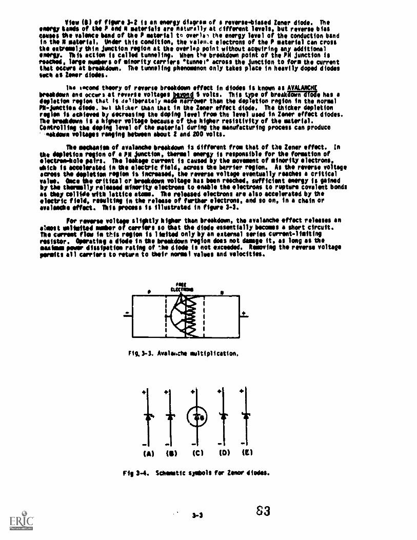
View if) of figure 3-2 is en energy diagrem of reverse-biesed Zener diode. Theenergy kends of the end N materiels ere nsturAlly et eifferent levels, but reverse biascameos the valence bend of the materiel to overlal the energy level of the conduction bandIn the N material. Under this condition, the valeme electrons of the materiel can crossthe extremely thin Junction region et the overlap point without acquiring any additionalenergy. Mit action is celled tunneling. When the breakdown point of the POI Junction isreaceed, large numbers of minority carriers *tunnei" across the junction to form the currentthat occurs et breakdown. The tunneling phenomenon only takes place in heavily doped diodessuch es loner diodes.
111411 4ftend theory of reverse breakdown effect in diodes is known es AVALANCNbreakdown and OCCW's et rows* voltages long 5 volts. This type of break own dod. has adepletion region that ts dalfberstaly ma6--Tiiffoaer then the depletion region in the normalIN -Jontion diode. bw1 thiater than that In the loner effect diode. The thicker depletionregion is aceieved bi decreasing the doping level from the level used In Zenor effect diodes.The breekdown Is a higher voltage because of the higher resistivity of the materiel.Controlling the depinn level of the materiel during the manufacturing process can produce-Innen voltages reeling between about 2 end 200 volts.
The @Khania of avalanche breakdown 13 different from that of the loner effect. In
the depletion region of a PO junction, thermal energy Is responsible for the formation ofelectrom-bele pairs. The leakage current Is caused by the movement of minority electrons,abich Is accelerated in the electric field, across the barrier region. As the reverse voltageacross the depletion region is increased, the reverse voltage eventually reaches a criticalvalve. One the critical or breakdown voltage hes been reached, sufficient energy Is gainedby the thornily released minority electrons to enable the electrons to rupture covalent bondsea they collide with lattice atoms. The released electrons are also accelerated by theelectric field, restating In the release of further electrons, end so on, In a chain orevelamche effect. This process Is illustrated In fipre 3-3.
For reverse voltage slightly higher than breakdown, the avalanche effect releases analmost onlimited number of carriers so that the diode essentially becomes a short circuit.The arrest flow in this region is limited only by en external series current-limitingresistor. Operating a dine in the breakdown region does not damage it, es long es themaximum power dissipatioe rating of the diode is not exceeded. Removing the reverse voltage
permits ell carriers to return to their normel values and velocities.
_fFig,3-3. Avalahche multiplication.
+ +
(A) fill (C) (0) (E)
Fig 3-4. Schematic symbols for Zenor diodes.
3-3 83

Some of the symbols used to represent Zenor diodes are illustrated in views (A)through (E) of figure 3-4. Note that the polarity markings indicate electron flow is with thearrow symbol instead of against it as in a normal PN-junction diode. This is becausebreakdown diodes are operated in the reverse-bias mode which means the current flow is byminority current carriers.
Zener diodes of various sorts are used for many purposes, but their most widespreaduse is as voltage regulators. Once the breakdown voltage of a Zener diode is reached, thevoltage across the dlode then remains almost constant regardless of the supply voltage.Therefore, they hold the voltage across the load at a constant level. This characteristicmakes Zener diodes ideal voltage regulators, and tney are found in almost all solid statecircuits ir this capacity.
The Tunnel Diode.
In 1958, Leo Esaki, a Japanese scientist, discovered that if a semiconductor junctiondiode is heavily doped with impurities, it will have a region of negative resistance. Thenormal junction diode uses semiconductor materials which are lightly doped with one impurityatom for ten million semiconductor atoms. This low doping level results in a relatively widedepletion region. Conduction occurs in the normal junction diode only if the voltage appliedto it is large enough to overcome the potential barrier of the junction.
In the TUNNEL DIODE, the'semiconductor materials used in forming a junction are dopedfor the extent Bir7iiriraiind impurity atoms for ten million semiconductor atoms. This heavydoping produces an extremely narrow depletion zone similar to that in the Zener diode. Alsobecause of the heavy doping, a tunnel diode exhibits an unusual current-voltage characteristiccurve as compared with that of an ordinary junction diode. The characteristic curve for atunnel diode is illustrated in figure 3-5.
- staftesa0 P Ao40.04%AWL Moot - peoes
Tmecou Goo toCTI1011041HISIHA Of C0'4
Fig 3-5. Characteristic curve of a tunnel diode comparedto that of a standard PM junction.
The three most important aspects of this characteristic curve are:(1) the forwardcurrent increase to a peak (1p) with a small applied forward bias, (2) the decreasingforward current with an increasing forward bias to a minimum valley current (Iv), and (3)the normal increasing forward current with further increases in the bias voltage. The portionof the characteristic curve between lp and Iv is the region of negative resistance. Anexplanation of why a tunnel diode has a region of negative resistance is best understood byusing energy levels as in the previous explanation of the Zener effect.
Simpty stated the theory known as quantum-mechanical tunneling is an electron crossinga PN junction without having sufficient energy to do so otherwise. Because of the heavydoping the width of the depletion region is only one-millionth of an inch. You might think cthe process simply as an arc-over between the N-and the P-side across the depletion region.
Figure 3-6 shows the equilibrium energy level diagram of a tunnel diode with no biasapplied. Note in view (A) that the valence band of the P-material overlaps the conductionband of the N-material. The majority electrons and holes are at the same energy level in theequilibrium state. If there is anymovement of current carriers across the depletion regiondue to thermal energy, the net current flow will be zero because equal numbers of currentcarriers flow in opposite directions. The zero net current flow is marked by an NO" on thecurrent-voltage curve illustrated in view (B).
3-4 0 4

CONDUCTIONSAND
FORBIDDENGAP
VALENCESAND
P -TYPE
CONDUCTIONSAND
FORSiDDENGAP
VALENCEBAND
N - TYPE
«v,00 100 000 600 500
v01./114C 11 MILLIVOI
...= IIANI04110 ITN JUNCTION
TUNNIL 01001- P0I11/11/HOMAN S INOICA/CPPOOPISSIOft 0 Cuolvt
(A) (B)
Fig 3-6. Tunnel diode energy diagram with no bias.
Figure 3-7, view (A), shows the energy diagram of a tunnel diode with a small forwardbias (50) millivolts) applied. The bias causes unequal energy levels between some of themajority carriers at the energy band overlap point, but not enough of a potential differenceto cause the carriers to cross the forbidden gap in the normal manner. Since the valence bandof the P-material and the conduction band of the N-material still overlap, current carrierstunnel across at the overlap and cause a substantial current flow. The amount of current flowis marked by point 2 on the curve in view (B). Note in view (A) that the amount of overlapbetween the valence band and the conduction band decreased when forward bias was applied.
CONDUCTIONSAND
FORBIDDENGAP
VALENCEBAND
P -TYPE
CONDUCTMNSAND
(A)
FORBIDDENGAP
I VALENCE IBAND
N - TYPE
5244011P0 PM JUNCTION
TUNNEL 01001- POINTS ITNROUGH 5 INDICIM21000055IO11 Or CLONE
100 200 SOO 600 500v001141 IN MILLIvOlTS
Fig 3-7. Tunnel diode energy diagram with 50 millivolts bias.
v
Figure 3-8, view (A), is the energy diagram of a tunnel diode in which the forwardbias has been increased to 450 millivolts. As you can see, the valence band and conductionband no longer overlap at this point, and tunneling can no longer occur. The portion of thecurve in view (B) from point 2 to point 3 shows the decreasing current that occurs as the biasis increased, and the area of overlap becomes smaller. As the overlap between the two energybands becoaes smaller, fewer and fewer electrons can tunnel across the junction. Tbe portionof the curve between point 2 and point 3 in which current decreases as the voltage increasesis the negative resistance region of the tunnel diode.
3-585

CONDUCTIONBAND
FORBIDDENGAP
MAKESAO
(A)
-v ........ V +VFORBIDDEN 100 200 SOO 400 000
GAP vOLsIGC IN MN.L.20LSS
VALENCE
e'GANG
N TYPE
crENDINCI N JuseCnON
TUNNEL 01001- CNNTS IIND1CSE
ONoGNISSION 0 CONN(
(B)
Fig 3-8. Tunnel diode energy diagram with 450 millivolts bias.
Figure 3-9, view (A), is the energy diagram of a tunnel diode in which the forwardbias has been increased even further. The energy bands no longer overlap and the diodeoperates in the same manner as a normal PN junction, as shown by the portion of the curve inview (B) from point 3 to point 4.
The negative resistance region is the most important and most widely usedcharacteristic of the tunnel diode. A tunnel diode biased to operae in the negativeresistance region can be used as either an oscillator or an amplifier in a wide range offrequencies and applications. Very high frequency applications usin, the tunnel action occursso rapidly that there is no transmit time effect and therefore no signal distortion. Tunneldiodes are also used extensively in high-speed switching circuits because of the speed of thetunneling action.
Several schematic symbol- are used to indicate tunnel diodes. These symbols areillustrated in views (A) through (D) of figure 3-10.
Varactor
The VARACTOR, or varicap, as the schematic drawing in figure 3-11 suggests, is a diodethat behaves like a variable capacitor, w;th the PN junction functioning like the dielectricand plates of a coomon capacitor. Understandint how the varactor operates is an importantprerequisite to understanding field-effect transistors, which will be covered later in thistopic.
CONDUCTIONBAND
FORBIDDEN FORBIDDENGAP GAP -V
VALENCESAND
N- TYPE
VALENCESAND
P -TYPE
(A)ELONKL MOH
JUNCTION
(RI
Fig 3-9. Tunnel diode energy diagram with 600 millivolts bias.
863-6
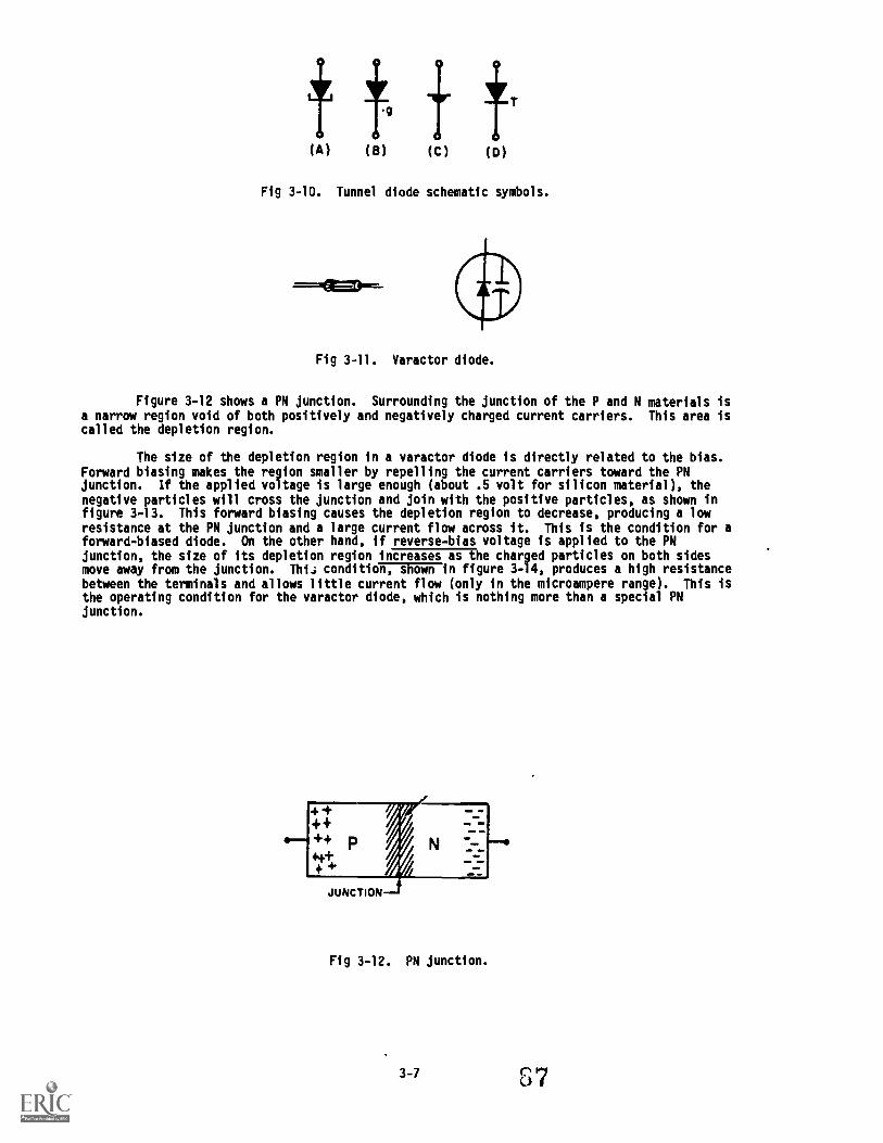
(C) (D)
Fig 3-10. Tunnel diode schematic symbols.
Fig 3-11. Varactor diode.
Figure 3-12 shows a PN junction. Surrounding the junction of the P and N materials isa narrow region void of both positively and negatively charged current carriers. This area iscalled the depletion region.
The size of the depletion region in a varactor diode is directly related to the bias.Forward biasing makes the region smaller by repelling the current carriers toward the PNjunction. If the applied voltage is large enough (about .5 volt for silicon material), thenegative particles will cross the junction and join with the positive particles, as shown infigure 3-13. This forward biasing causes the depletion region to decrease, producing a lowresistance at the PN junction and a large current flow across it. This is the condition for aforward-biased diode. On the other hand, if reverse-bias voltage is applied to the PNjunction, the size of its depletion region increases as the charged particles on both sidesmove away from the junction. This; conditioW7W5Wrin figure 3-14, produces a high resistancebetween the terminals and allows little current flow (only in the microampere range). This isthe operating condition for the varactor diode, which is nothing more than a special PNjunction.
Fig 3-12. PN junction.

4-44"- N
40.!...4
Fig 3-13. Forward-biased PN Junction.
As the figure shows, the insulation gap formed by reverse biasing the varactor iscomparable to the layer of dielectric material between the plates of a common capacitor.Furthermore, the formula used to calculate capacitance can be applied to both the varactor andthe capacitor. In this case, the size of the insulation gap of the varactor, or depletionregion, is substituted for the distance between the plates of the capacitor. By varying thereverse-bias voltage applied to the varactor, the width of the "gap" may be varied. Anincrease in reverse bias increases the width of the gap (d) which reduces the capacitance (C)WITIFPN Junction. Merl-M-7375e capacitance of the varactor is inversely proportional tothe applied reverse bias.
Where:
GAP
Fig 3-14. Reverse-biased PN Junction.
DEPLETIONREGION
6V
(B)
Fig 3-15. Varactor capacitance versus bias voltage.
A = plate area
K = a constant value
d = distance between plates
3-8
68

The ratio of varactor capacitance to reverse-bias voltage change may be as high as 10to 1. Figure 3-15 shows one example of the voltage-to-capacitance ratio. View (A) shows thata verse bias of 3 volts produces a capacitance of 20 picofarads in the varactor. If thereverse bias is increased to 6 volts, as shown in view (B), the depletion region widens andcapacitance drops to 5 picofarads. Each 1-volt increase in bias voltage causes a 5-picofaraddecrease in the capacitance of the varactor; the ratio of change is therefore 5 to 1. Ofcourse any decrease in applied bias voltage would cause a proportionate increase incapacitance:7W depletion region narrows. Notice that the value of t e capacitance issmall in the picofarad range.
In general, varactors are used to replace the old style variable capacitor tuning.Thea are used in tuning circuits of more sophisticated communication equipment and in othercircuits where variable capacitance is required. One advantage of the varactor is that itallows a d.c. voltage to be used to tune a circuit for simple remote control or automatictuning functions. One such application of the varactor is as a variable tuning capacitor in areceiver or transmitter tank circuit like that shown in figure 3-16.
Figure 3-16 shows a d.c. voltage felt at the wiper of potentiometer R1 which can beadjusted between +V and -V. The d.c. voltage, passing through the low resistance of radiofrequency choke L2, acts to reverse bias varactor diode C3. The capacitance of C3 is inseries with C2, and the equivalent capacitance of C2 and C3 is in parallel with tank circuitLl-Cl. Therefore, any variation in the d.c. voltage at R1 will vary both the capacitance ofC3 and the resonant frequency of the tank circuit. The radio-frequency choke provides highinductive reactance at the tank frequency to prevent tank loading by Rl. C2 acts to blockd.c. from the tank as well as to fix the tuning range of C3.
An ohmmeter can be used to check a varactor diode in a circuit. A high reverse-biasresistance and a low forward-bias resistance with a 10 to 1 ratio in reverse-bias toforward-bias resistance is considered normal.
Ri
-v
Fig 3-16. Varactor tuned.
EXERCISE: Answer the following questions and check your responses against those listed atthe end of this study unit.
1. In a reverse-biased PN junction, which current carriers cause leakage current?
2. The action of a PN Junction during breakdown can be explained by what two theories?
0.
b.
3. Which breakdown theory explains the action that takes place in a heavily doped PNJunction with a reverse bias of less than 5 volts?
4. What is the doping level of an avalanche effect diode when compared to the dopinglevel of a zener effect diode?
3-9

5. Durg avalanche effect breakdown, what limits current flow through the diode?
6. liety is electron flow with the arrow in the symbol of a zener diode instead ofagainst the arrow as it is in a normal diode?
7. What is the main difference in construction between normal PN junction diodes andtunnel diodes?
8. What resistance property is found in tunnel diodes but not in normal diodes?
9. When compared to the ordinary diode, the tunnel diode has what type of depletionregion?
10. In the tunnel diode, the tunneling current is at what level when the forbidden gapcf the N-type material is at the same energy level as the empty states of theP-type material?
11. The varactor displays what useful electrical property?
12. When a PN junction is forward biased, what happens to the depletion region?
13. When the reverse bias on a varactor is increased what happens to the effectivecapacitance?
Work Unit 3-2. SILICON COMTROLLED RECTIFIER (SCR)
EXPLAIN THE BASIC OPERATION OF THE SILICON CONTROLLED RECTIFIER.
EXPLAIN THE BASIC OPERATION OF THE TRIAC.
COMPARE THE ADVANTAGES AND DISADVANTAGES OF THE SILICON CONTROLLED RECTIFIER ANDTRIAC.
The SILICON CnNTROLLED RECTIFIER, usually referred to as ri SCR, is one of the familyof semiconductors that includes transistors and diodes. A drawing of an SCR and its schematicrepresentation is thown in views (A) and (B) of figure 3-17. Not all SCRs use the casingshown, but this is typical of most of the high-power units.

(A)
A. A high Power unit.13. The schematic symbol.
ANODE
DATE LEAD
CATHODE
LEAD
(a)
Fig 3-17. Silicon controlled rectifier.
Although it is not the same as either a diode or a transistor, the SCR combinesfeatures of both. Circuits using transistors or rectifier diodes may be greatly improved insome instances through the use of SCRs.
The basic purpose of the SCR is to function as a switch that can turn on or off smallor large amounts of power. It performs this function with no moving parts that wear out andno points that require replacing. There can be a tremendous power gain in the SCR; in someunits a very small triggering current is able to switch several hundred amperes withoutexceeding its rated abilities. The SCR can often replace much slower and larger mechanicalswitches. It even has many adVantages over its more complex and larger electronic-tubeequivalent, the thyratron.
The SCR is an extremely fast switch. It is difficult to cycle a mechanical switchseveral hundred times a minute, yet, some SCRs can be switched 25,000 times a second. Ittakes just microseconds (millionths of a second) to turn on or off these units. Varying thetime that a switch is on as compared to the time that it is off regulates the amount of powerflowing through the switch. Since most devices can operate on pulses of power (alternatingcurrent is a special form of alternating positive and negative pulses), the SCR can be usedreadily in controlled applications. Motor-speed controllers, inverters, remote switchingunits, controlled rectifiers, circuit overload protectors, latching relays, and computer logiccircuits all use the SCR.
The SCR is made up of four layers of semiconductor material arranged PNPN. Theconstruction is shown in view (A) of figure 3-18. In function, the SCR has much in commonwith a diode, but the theory of operation of the SCR is best explained in terms of transistors.
Consider the SCR as a transistor pair, one PNP and the other NPN, connected as shownin views (B) and (C). The anode is attached to the upper P-layer; and the gate terminal, G,goes tc the P-layer of the NPN triode.
In operation, the collector of Q2 drives the base of Ql, while the collector of Q1feeds back to the base of Q2. 131 (Beta) is the current gain of Ql, and B2 is the current gainof Q2. The gain of this positive feedback loop is their product, Iil times 82. When theproduct is less than one, the circuit is stable; if the product is greater than unity, thecircuit is regenerative. A small negative current applied to terminal G will bias the NPNtransistor into cutoff, and the loop gain is less than unity. Under these conditions, theonly current that can exist between output terminals A and C is the very small cutoffcollector current of the two transistors. For this reason the impedance between A and C isvery high.

ANODE
J I
GAT EJ 2
j 3
CAT40.
(A)
(C)
A. Paris of an SCR.B. Two.lransistor equivaknt.C. Two-transistor schematic.
Fig 3-18. SCR structure.
-c
When a positive current is applied to terminal G, transistor Q2 is biased intoconduction, causing its collector current to rise. Since the current gain of Q2 increaseswith increased collector current, a point (called the breakdown point) is reached where theloop gain equals unity and the circuit becomes regenerative. At this point, collector currentof the two transistors rapidly increases to a value limited only by the external circuit.Both transistors are driven into saturation, and the impedance between A and C is very low.The positive current applied to terminal G, which served to trigger the self-regenerativeaction, 13 no longer required since the collector of PNP transistor Q1 now supplies more thanenough current to drive Q2. The circuit will remain on until it is turned off by a reductionin the collector current to a value below that necessary to maintain conduction.
NIGN CONDUCTION
HOLD:NG CURRENT
REVERSE anon:menVOLTAGE VOLTAGE
ARE AK DO* Nyc, LTAGE
LEAKAGECURRENT FORWARD
LEAKAGECURRENT
FORWARDV OLYAGE
Fig 3-19. Characteristic curve for an SCR.
The characteristic curve for the SCR is shown in figure 3-19. With no gate current,the leakage current remains very small as the forward voltage from cathode to anode isincreased until the breakdown point is reached. Here the center junction breaks down, the SCRbegins tn conduct heavily, and the drop across the SCR becomes very low.
3-12 92

The effect of a gate signal on the firing of an SCR is shown in figure 3-20.Breakdown of the center junction can be achieved at speeds approaching a microsecond byapplying an appropriate signal to the gate lead, while holding the anode voltage constant.After breakdown, the voltage across the device is so low that the current through it fromcathode to anode is essentially determined by the load it is feeding.
The important thing to remember is that a small current from gate to cathode can fireor trigger the SCR, changing it from practically an open circuit to a short circuit. The onlyway to change it back again (to commutate it) is to reduce the load current to a value lessthan the minimum forward-bias current. Gate current is required only until the anode currenthas completely built up tO a point sufficient to sustain conduction (about 5 microseconds inresistive-load circuits). After conduction from cathode to anode begins, removing the gatecurrent has no effect.
The basic operation of the SCR can be compared to that of the thyratron. Thethyratron is an electron tube, normally gas filled, that uses a filament or a heater. The SCRand the thyratron function in a very similar manner. Figure 3-21 shows the schematic of eachwith the corresponding elements labeled. In both types of devices, control by the inputsignal is lost after they are triggered. The cuntrol grid (thyratron) and the gate (SCR) haveno further effect on the magnitude of the load current after conduction begins. The loadcurrent can be interrupted by one or more of three methods (1) the load circuit must be openedby a switch, (2) the plate (anode) voltage must be reduced below the ionizing potential of thegas (thyratron). (3) the forward-bias current must be reduced below a minimum value requiredto sustain conduction (SCR). The input resistance of the SCR is relatively low (approximately100 ohms) and requires a :..urrent for triggering; the input resistance of the thyratron is
exceptionally high, and requires a voltage input to the grid for triggering action.
MAMMutilREvERSEVOLTAGE
HOLDINGCURRENT
HIGH CONDUCTIONREGION
zo
zoo
REvERSEAVALANCHE
REGION
REVERSEBLOCKING
REGION
cORwARDBLOCKING
REGION
°MK
FORWARDOREAKOVER
VOLTAGE(rORWARD
AVALANCHE REGION)
Fig 3-20. SCR characteristic curve with various gate signals.
A. SCR.
PLATE
B. Thyrelron
Fig 3-21. Comparison of an SCR and a thyratron.
The applications of the SCR as a rectifier are many. In fact, its many applicationsas a rectifier give this semicondUctor device its name. When alternating current is appliedto a rectifier, only the positive or negative halves of the sine waves flow through. All ofeach positive or negative half cycle appears in the output. When an SCR is used, however, thecontrolled rectifier may be turned on at any time dur!ng the half cycle, thus controlling the
3-13
93

amount of d.c. power available from zero to maximum, as shown in figure 3-22. Since theoutput is actually d.c. pulses, suitable filtering can be added if continuous direct currentis needed. Thus any d.c. operated device can have controlled amounts of power applied to it.Notice that the SCR must be turned on at the desired time tor each cycle.
When an a.c. power source is used, the SCR is turned off automatically, since thecurrent and voltage drop to zero every half cycle. By using one SCR on positive alternationsand one on negative, full-wave rectification can be acomplished, and control is obtainedover the entire sine wave. The SCR serves in this application just as its name implies-as acontrolled rectifier of a.c. voltage.
GATE PHASE DELAYPULSE 0° MAL
OUTPUT
00 FIRING ANGLE
180° CONDUCTION ANILE,
PHASE DELAYGATE PULSE
900 HALF MAX.OUTPuT
900 FINING ANGLE
900 COND. ANGLE
GATE PHASE DELAY
PULSE MO°NG OUTPuT
190° FIRING ANGLE
0° COND. ANGLE
Fig 3-22. SCR gate control signals.
7he TRIAC is a three-terminal devise similar in construction and operation to theSCR. The triac controls and conducts current flow during both alternations of an a.c. cycle,instead of only one. The schematic symbols for the SCR anaTige triac are compared in figure
Both the SCR and the triac have a gate lead. However, in the triac the lead on thesame side as the gate is "main terminal 1," and the lead opposite the gate is "main terminal2." This method of lead labeling is necessary because the triac is essentially two SCRs backto back, with a common gate and common terminals. Each terminal is, in effect, the anode ofone SCR and the cathode of another, and either terminal can receive an input. In fact, thefunctions of a triac can be duplicated by connecting two actual SCRs as shown in figure 3-24.The result is a three-terminal device identical to the triac. The common anode-cathodeconnections form main terminals 1 and 2, and the common gate forms terminal 3.
-GATE
ANODE CATHODE
GATE
MAWTERMWAL
1
SCR
TRIAC
MAINTERMINAL
2
Fig 3-23. Comparison of SCR and TRIAC symbols.
The difference in current control between the SCR and the triac can be seen bycomparing their operation in the basic circuit shown in figure 3-25.
3-14J°4
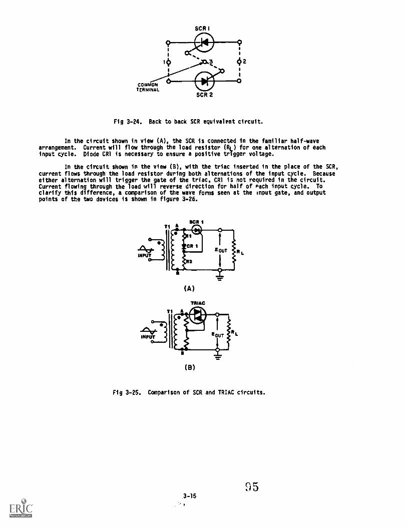
SCR I
COMMONTERMMAL
SCR 2
Fig 3-24. Back to back SCR equivalent circuit.
In the circuit shown in view (A), the SCR is connected in the familiar half-wavearrangement. Current will flow through the load resistor (RL) for one alternation of eachinput cycle. Diode CR1 is necessary to ensure a positive trigger voltage.
In the circuit shown in the view (B), with the triac inserted in the place of the SCR,current flows through the load resistor during both alternations of the input cycle. Becauseeither alternation will trigger the gate of the triac, CR1 is not required in the circuit.Current flowing through the load will reverse direction for half of Pilch input cycle. Toclarify this difference, a comparison of the wave forms seen at the input gate, and outputpoints of the two devices is shown in figure 3-26.
(A)
TRIAC
(a)
Fig 3-25. Comparison of SCR and TRIAC circuits.
c'd 53-15

(lateTrigger!Level I
InputVoltage
GateVoltage
OutputVoltage:
SCR
-r
GateTriggerLevel
----J
Fig 3-26. Comparison of SCR and TRIAC waveforms.
EXERCISE: Answer the following questions and check your responses agenst those listed atthe end of the study unit.
1. The SCR is primarily used for what function?
2. When an SCR is forward biased, what is needed to cause it to conduct?
3. What is the only way to cause an SCR to stop conducting?
4. The triac is similar in operation to what device?
5. When used for a.c. current control, during which alternation of the a.c. cycledoes the triac control current flow?
Work Unit 3-3. OPTOELECTRONIC DEVICES
LIST THE FIVE MOST COMMONLY USED OPTOELECTRONIC DEVICES.
EXPLAIN THE USES OF THE FIVE MOST COMMONLY USED OPTOELECTRONIC DEVICES.
PICT7IONIC devices either produce light or use light in their operation. Thefirst rht.y, the light emitting diode (LED), was developed to replace the fragile,short-lite incoadescent light bulbs used to indicate on/off conditions on panels. A LIGHTEMITTING mom is a diode which, when forward biased, produces visible light. The light maybe red, green, or amber, depending upon the material used to make the diode.
Fig 3-27. LED.
3-16
961

(B)
Fig 3-28. Seven-segment LED display.
Figure 3-27 shows an LED and its schematic synbol. The LED is designated by a
standard diode symbol with two arrows pointing away from the cathode. The arrows indicate
light leaving the diode. The circuit symbols for all optoelectronic devices have arrowspointing either towards them, if they use light, or away from them, if they produce light.The LED operating voltage is small, agiE 1.6 volts forward bias and general y about 10milliamperes. The life expectancy of the LED is very long, over 100,000 hours of operation.
(A) (B)
Fig 3-29. Seven segment LED display examples.
Fig 3-30. Stacked seven-segment display.
LEDs are used widely as "power on" indicators of current and as displays for pocket
calculators, digital voltmeters, Wrfr'equency counters. For use in calculators and similardevices, LEDs are typically placed together in seven-segment displays, as shown in figure
3-28. This display uses seven LED segments, or bars (labeled A through G in the figure),which can be lit in different combinations to form any number from "0" through "9." The
schematic, view (A), shows a common-anode display. All anodes in a display are internally
connected. When a negative voltage is applied to the proper cathodes, a number is formed.For example, if negative voltage is applied to all cathodes except that of LED "E" the number119" is produced, as shown in view (A) of figure 3-29. If the negative voltage is changed and
applied to all cathodes except LED "B," the number "9" changes to "6" as shown in view (B).

Seven-segment displays are also available in common-cathode form, in which allcathodes are at the same potential. When replacing LED displays, you must ensure thereplacement display is of the same type as the faulty display. Since both types look alike,you should always check the manufacturer's number.
LEO seven-segment displays range from the very small, often not much larger thanstandard typewritten numbers, to about an inch. Several displays may be combined in a packageto show a series of numbers, such as the one shown in figure 3-30.
Another special optoelectronic device in common use today is the photodiode. Unlikethe LED, which produces light, the photodiode uses light to accomplish special circuitfunctions. Basically, the PHOTOOIODE is a light-controlled variable resistor. In totaldarkness, it has a relatively high resistance and, therefore, conducts little current.However, when the PH junction is exposed to an external light source, internal resistancedecreases and current flow increases. The photodidde is operated with reverse bias andconducts current in direct proportion to the intensity of the light source.
Figure 3-31 shows a photodiode with its schematic symbol. The arrows pointing towardthe symbol indicate that light is required for operation of the device. A light source isaimed at the photodiode through a transparent "window" placed over the semiconductor chip.Switching the light source on or off changes the conduction level of the photodiode. Varyingthe light intensity controls the amount of conduction. Because photodiodes respond quickly tochanges in light intensity, they are extremely useful in digital applications such as computercard readers, paper tape readers, and photographic light meters. They are also used in sometypes of optical scanning equipment.
11..E)
Fig 3-31. Photodiode.
Fig 3-32. Phototransistor.
PNP NPN
EC)NPN PNP
Fig 3-33. 2-Terminal and 3-terminal phototransistors.
83-18
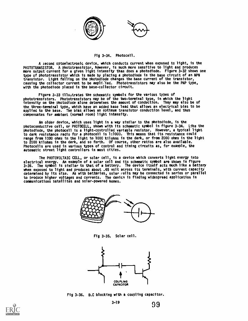
Fig 3-34. Photocell.
A second optoelectronic device, which conducts current when exposed to light, is the
PHOTOTRANSISTOR. A phototransistor, however, is much more sensitive to light and producesmore output current for a given light intensity than does a photodiode. Figure 3-32 shows one
type of phototransistor which is made by placing a photodiode in the base circuit of an NPNtransistor. Light falling on the photodiode changes the base current of the transistor,causing the collector current to be amplified. Phototransistors may also be the PNP type,
with the photodiode placed in the base-collector circuit.
Figure 3-33 illuArates the schematic symbols for the various types ofphototransistors. Phototransistors may be of the two-terminal type, in which the lightintensity on the photodiode alone determines the amount of conduction. They may also be of
the three-terminal type, which have an added base lead that allows an electrical bias to beapplied to the base. The bias allows an optimum transistor conduction level, and thuscompensates for ambient (normal room) light intensity.
An older device, which uses light in a way similar to the photodiode, is thephotoconductive cell, or PHOTOCELL, shown with its schematic symbol in figure 3-34. Like the
photodiode, the photocell is a light-controlled variable resistor. However, a typical lightto dart resistance radio for a photocell is 1:1000. This means that its resistance couldrange from 1000 ohms in the light to 1000 kilohms in the dark, or from 2000 ohms in the lightto 2000 kilohms in the dark, and so forth. Of course, other ratios are also available.Photocells are used in various types of control and timing circuits as, for example, theautomatic street light controllers in most cities.
The PHOTOVOLTAIC CELL, or solar cell, is a device which converts light energy intoelectrical energy. An example of a solar cell and its schematic symbol are shown in figure3-35. The symbol is similar to that of a battery. The device itself acts much like a battery
when exposed to light and produces about .45 volt across its terminals, with current capacitydetermined by its size. As with batteries, solar cells may be connected in series or parallel
to produce higher voltages and currents. The device is finding widespread application incommunications satellites and solar-powered homes.
Fig 3-35. Solar cell.
I I
COUPLINGCAPACITOR
Fig 3-36. D.0 blocking with a coupling capacitor.
3-19 99

PHOTODIODE
LED
Fig 3-37. Optical coupler.
When it is necessary to block the voltage between one electronic circuit and another,and transfer the signal at the same time, an amplifier coupling capacitor is often used asshown in figure 3-36. Although this method of-coupling does block d.c. between the circuits,voltage isolation is not complete. A newer method, making use of optoelectronic devices toachieve electrical isolation, is the optical coupTer, shown in figure 3-37. The coupler iscomposed of an LED and a photodiode contained in a light-conducting medium. As the polaritysigns in figure 3-37 show, the LED is forward bias, while the photodiode is reverse biased.When the input signal causes current through the LED to increase, the light produced by theLED increases. This increased light intensity causes current flow through the photodiode toincrease. In this way, changes in input current produce proportional changes in the output,even though the two circuits are electrically isolated.
The optical coupler is suitable for frequencies in the low megahertz range. Thephotodiode type shown above can handle only small currents; however, other types of couplers,combining phototransistors with the SCR, can be used where more output is required. Opticalcouplers are replacing transformers in low-voltage and low-currEnt applications. Sensitivedigital circuits can utilize the coupler to control large current and voltages withlow-voltage logic levels.
EXERCISE; Answer the following questions and check your responses against those listed atthe end of this study unit.
1. What type of bias is required to cause an LED to produce light?
2. When compared to incandescent lamps, what is the power requirement of an LED?
3. In a common anode, a seven-segment LED display, an individual LED will light if anegative voltage is applied to what element?
4. What is the resistance level of a photodiode in total darkness?
5. What type of bias is required for proper operation of a photodiode?
6. What is a typical light-to-dark resistance ratio for a photocell?
7. What semiconductor device produces electrical energy when exposed to light?
Work Unit 3-4. TRANSISTORS
DESCRIBE THE BASIC OPERATION, APPLICATIONS, AND MAJOR ADVANTAGES OF THEUNIJUNCTION TRANSISTOR.
3-20100

DESCRIBE THE BASIC OPERATION, APPLICATIONS, AND MAJOR ADVANTAGES OF THEFIELD-EFFECT TRANSISTOR.
DESCRIBE THE BASIC OPERATION, APPLICATIONS AND MAJOR ADVANTAGES OF THE METAL OXIDESEMICONDUCTOR FIELD EFFECT TRANSISTOR.
Transistors are semiconductor devices with three or more terminals. The operation of
normal transistors has already been discussed, but there are several transistors with special
properties that should be explained. As with diodes, a discussion of all the developments in
the transistor field would be impossible. The unijunction transistor (UJT) and thefield-effect transistor (FET) will be discussed because of their widespread application in
Marine Corps equipment.
The UNIJUNCTION TRANSISTOR (UJT), originally called a double-based diode, is a
three-terminal, solid-state device that has several advantages over conventional transistors.
It is very stable over a wide range of temperatures and allows a reduction of components when
used in the place of conventional transistors. A comparison is shown in figure 3-38. View
(A) is a circuit using conventional transistors, and view (B) is the same circuit using the
UJT. As you can see, the UJT circuit has fewer components. Reducing the number of components
reduces the cost, size, and probability of failure.
The physical appearance of the UJT is identical to that of the common transistor. As
shown in figure 3-39, both have three leads and the same basic shape; the tab on the case
indicates the emitter on both devices. The UJT, however, has a second base instead of a
collector.
As indicated in the block diagram shown in views (A) and (B) of figure 3-40, the lead
differences are even more pronounced. Unlike the transistor, the UJT has only one PN
junction. The area between base 1 and base 2 acts as a resistor when the UJT is properly
biased. A conventional transistor needs a certain bias level between the emitter, base, and
collector for proper conduction. The same principle ic true for the UJT: it needs a certain
bias level between the emitter and base 1 and also between base 1 and base 2 for proper
conduction.
The normal bias arrangement for the UJT is illustrated in figure 3-41, view (A). A
positive 10 volts is placed on base 2 and a ground on base 1. The area between base 1 and
base 2 then acts as a resistor. If a reading were taken between base 1 and base 2, the meter
would indicate the full 10 volts as shown in view (B). Theoretically, if one meter lead was
connected to base 1 and the other lead to some point between base 1 and base 2, the meter
could read some voltage less than 10 volts. This concept is illustrated in figure 3-42, view
(A). View (B) is an illustration of the voltage levels at different points between the two
bases. The sequential rise in voltage is called a voltage gradient.
(A)
A. Transistor. B. UJT.
Fig 3-38. Comparison of conventional transistor and UJT circuits.
3-21 101

(A)
A. Transistor.
(B)
B. WT.
Fig 3-39. Transistor and UJI.
The emitter of the UJT can be viewed as the wiper arm of a variable resistor. If thevoltage level on the emitter is more positive than the voltage gradient level at theemitter-base material contact point, then the UJT is forward biased. The UJT will conductheavily (almost a short circuit) from base 1 to the emitter. The emitter is fixed in positionby tha manufacturer. The level of the voltage gradient, therefore, depends upon the amount ofbias voltage, as shown in figure 3-43.
(A)
A. Transistor.
PTYPEMATERIAL
I JUNCTION
82
(B)
B. WT.
N - TTPEMATERIAL
Fig 3-40. Transistor and UJT structure.
al
,1=11
(A)
Cc
(B)
Fig 3-41. UR biasing.
(A)
41"CCKW
OV1+ 6V
+41/
211
*OV
(B
Fig 3-42. UJT voltage gradient.
3-22
102

Fig 3-43. Forward bias point on UJT voltage gradient.
If the voltage level on the emitter is less positive than the voltage gradient
opposite the emitter, the UJT is then reverse biased. No current will flow from base 1 to the
emitter. However, a small current, called reverse current, will flow from the emitter to base
2. The reverse current is caused by the impurities used in the construction of the UJT and is
in the form of minority carriers.
More than forty distinct types of UJTs are presently in use. One of the most common
applications is in switching circuits. They are also used extensively in oscillators and wave
shaping circuits.
Although it has brought about a revolution in the design of electronic equipment, the
bipolar (PNP/NPN) transistor still has one very undesirable characteristic. The low input
impedance associated with its base-emitter junction causes problems in matching impedances
between interstage amplifiers.
For years, scientists searched for a solution which would combine the high input
impedance of the vacuum tube with the many other advantages of the transistor. The result of
this research is the FIELD-EFFECT TRANSISTOR (FET). In contrast to the bipolar transistor,
which uses bias current between base and emitter to control conductivity, the FET uses voltage
to control an electrostatic field within the transistor. Because the FET is
voltage-controlled, much like a vacuum tube, it is sometimes called the "solid state vacuum
tube."
The elements of one type of FET, the junction type (JFET), are compared with the
bipolar transistor and the vacuum tube in figure 3-44. As the figure shows, the JFET is a
three-element device comparable te the other two. The "gate" element of the JFET corresponds
very closely in operation to the base of the transistor and the grid of the vacuum tube. The
"source" and "drain" elements of the JFET correspond to the emitter and collector of thetransistor and to the cathode and plate of the vacuum tube.
The construction of a JFET is shown in figure 3-45. A solid bar, made either of
N-type or P-type material, forms the main body of the device. Diffused into each side of this
bar are two deposits of material of the opposite type from the bar material, which form the
"gate." The portion of the bar between the deposits of gate material is of a smaller crosssection than the rest of the bar and forms a "channel" connecting the source and the drain.
Figure 3-45 shows a ben. of N-type materiai and a gate of P-type material. Because the
material in the channel is N-type, the device is called an N-channel JFET.
COLLECTOR
BIPOLAR
DRAIN
GATE GRIO
PLATE
SOURCE 0 CATHODE
JFET VACUUM TUBE
Fig 3-44. Comparison of JFET, transistor and vacuum tube symbols.
3-23
103

OATS
DRAIN
N-TTRESILICON SAN
DIFFUSEDP.TTPEMATERIAL
Fig 3-45. JFET structure.
In a P-channel JFET, the channel is made of P-type material and the gate of N-typematerial. In figure 3-46, schematic symbols for the two types of JFET are compared with thoseof the NPN and PNP bipolar transistor. Like the bipolar transistor types, the two types ofJFET differ only in the configuration of bias voltages required and in the direction of thearrow within the symbol. Just as it does in transistor symbols, the arrow in a JFET symbolalways points towards the N-type macerial. Thus, the symbol of the N-material JFET shows thearrow pointing towards the drain/source channel;whereas, the P-channel symbol shows the arrowpointing away from the drain/source channel, towards the gate.
CAR
1+)s-o.)
1-)
NPN TRANSISTOR
DRAIN 10
Of
SOURCE I-I
11CNANNEL IFET
I-)
(+)
PNP TRANSISTOR
DRAIN H
SOURCE (+)
PENANNEL IFET
Fig 3-46. Symbols and bias voltages for transistors and JFET.
Fig 3-47. JFET operation with zero gate bias.
The key to FET operation is the effective cross-se-tional area of the channel, whichcan be controlled by variations in the voltage applied to the gate. This is demonstrated inthe figures which follow.
Figure 3-47 shows how the JFET operates in a zero gate bias condition. Five volts areapplied across the JFET so that current flows through the bar from source to drain, asindicated by the arrow. The gate terrinal is tied to ground. This is a zero gate biascondition. In this condition, a typica; bar represents a resistance of about 500 ohms. A
3-24
104

millimeter, connected in series with the drain lead and d.c. power, indicates the amount of
current flow. With a drain supply (VDD) of 5 volts, the milliammeter gives a drain current
(Ip) reading of 10 milliamperes. The voltage and current subscript letters (VDD, Ip)
used for an FET correspond to the elements of the FET just as they do for the elements of
transistors.
In figure 3-48, a small reverse-bias voltage is applied to the gate of the JFET. A
gate-source voltage (VGG) of negative 1 volt applied to the P-type gate material causes the
junction between the P- and N-type material to become reverse biased. Just as it did in the
varactor diode, a reverse-bias condition causes a "depletion region" to form around the PN
junction of the JFET. Because this region has a reduced number of current carriers, the
effect of reverse biasing is to reduce the effective cross-sectional area of the "channel."
This reduction in area increases the source-to-drain resistance of the device and decreases
current flow.
vaa
Fig 3-48. FET with reverse bias.
The application of a large encugh negative voltage to the gate will cause the
depletion region to become so large that conduction of current through the bar stops
altogether. The voltage required to reduct drain current (Ip) to zero is called "pinch-off"
voltage and is comparable to "cuff-off" voltage in a vacuum tube. In figure 3-48, the
negative 1 volt applied, although not large enough to completely stop conduction, has caused
the drain current to decrease markedly (from 10 milliamperes). Calculation shows that the
1-volt gate bias has also increased the resistance of the JFET (from 500 ohms to 1 kilohm).
In other words, a 1-volt change in gate voltage has doubled the resistance of the device and
cut current flow in half.
.SrA
Fig 3-49. JFET input impedance.
These measurements, however, show only that a JFET operates in a manner similar to a
bipolar transistor, even though the two are constructed differently. As stated before, the
main advantage of an FET is that its input impedance is significantly higher than that of a
bipolar transistor. The higher input impedance of the JFET under reverse gate bias conditions
can be Seen by connecting a microammeter in series with the gate-source voltage (VGG), as
shown in figure 3-49.
3-25 105

With a VGG of 1 volt, the microammeter reads .5 microamps. Applying Ohm's law(1 V ; .5u A) ilTustrates that this very small amount of current flow results in a very highinput impedance (about 2 megohms). By contrast, a bipolar transistor in similar circumstanceswould require higher current flow (e.g., .1 to -1 mA), resulting in a much lower inputimpedance (about 1000 ohms or less). The higher input impedance of the JFET is possiblebecause of the way reverse-bias gate voltage affects the cross-sectional area of the channel.
The preceding example of JFET operation uses an N-channel JFET. However, a P-channelJFET operates on identical principles. The differences between the two types are shown infigure 3-50.
Because the materials used to make the bar and the gate are reversed, source voltagepotentials must also be reversed. The P-channel JFET, therefore, requires a positive gatevoltage in order to be reverse biased, and current flows through it from drain to source.
Figure 3-51 shows a basic common-source amplifier circuit containing an N-channelJFET. The characteristics of this circuit include high input impedance and a high voltagegain. The function of the circuit components in this figure is very similar to those in atriode vacuum tube common-cathode amplifier circuit. Cl and C3 are the input and outputcoupling capacitors. R1 is the gate return resistor and functions much like the grid returnresistor in a vacuum tube circuit. It prevents unwanted charge buildup on the gate byproviding a discharge path for Cl. R2 and C2 provide source self-bias for the JFET, whichoperates like cathode self-bias. R3 is the drain load resistor, which acts like the plate orcollector load resistor.
OMON 144
(.4
0 DRAIN
CIAT011.4a)4.)
I e 101
BOLINCII
ONA1N
1+1 *OUNCE
0110UNCIN-EHANNEL JFET
P-CHANNEL JFET
Fig 3-50. JFET symbols and bias voltages.
Fig 3-51. JFET common source amplifier.
3-26 106
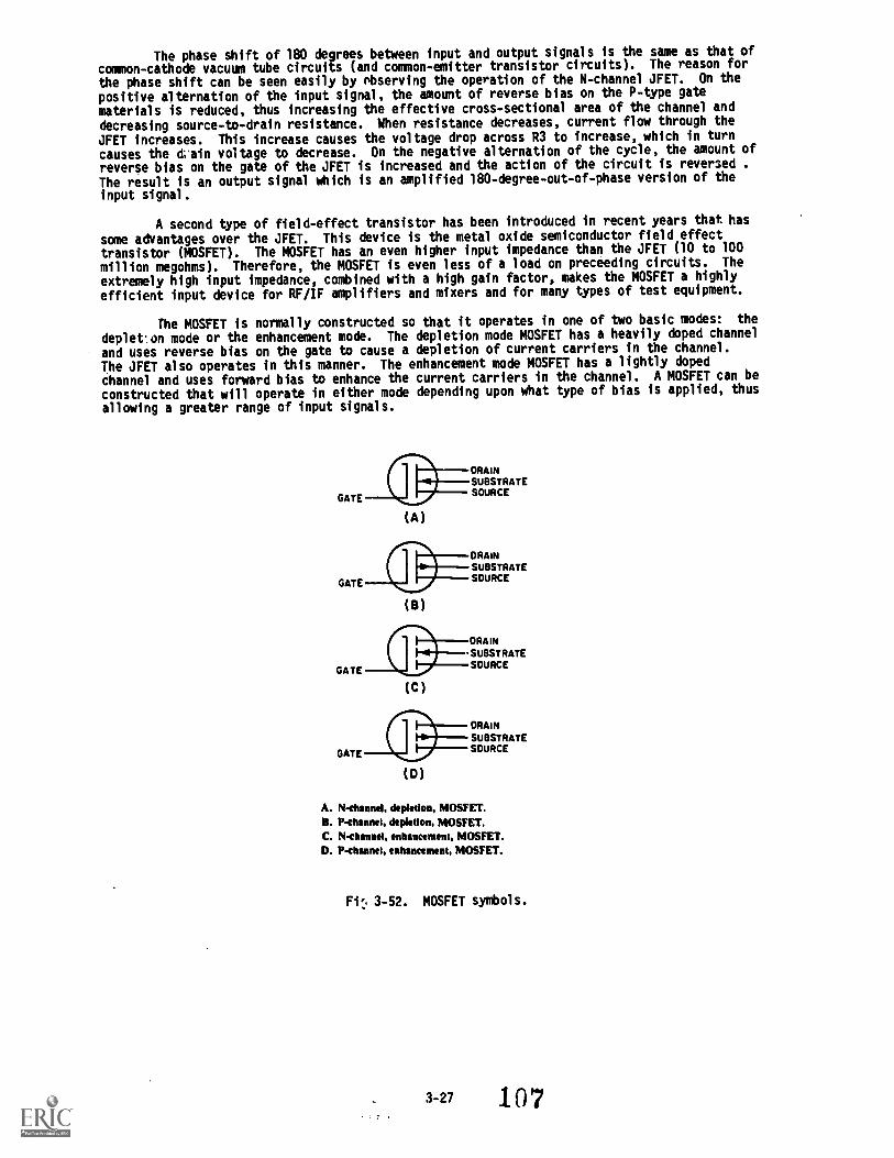
The phase shift of 180 degrees between input and output signals is the same as that of
common-cathode vacuum tube circuits (and common-emitter transistor circuits). The reason for
the phase shift can be seen easily by observing the operation of the N-channel JFET. On the
positive alternation of the input signal, the amount of reverse bias on the P-type gate
materials is reduced, thus increasing the effective cross-sectional area of the channel and
decreasing source-to-drain resistance. When resistance decreases, current flow through the
JFET increases. This increase causes the voltage drop across R3 to increase, which in turn
causes the chain voltage to decrease. On the negative alternation of the cycle, the amount of
reverse bias on the gate of the JFET is increased and the action of the circuit is reversed .
The result is an output signal which is an amplified 180-degree-out-of-phase version of the
input signal.
A second type of field-effect transistor has been introduced in recent years that has
some adVantages over the JFET. This device is the metal oxide semiconductor field effect
transistor (MOSFET). The MOSFET has an even higher input impedance than the JFET (10 to 100
million megohms). Therefore, the MOSFET is even less of a load on preceeding circuits. The
extremely high input impedance, combined with a high gain factor, makes the MOSFET a highly
efficient input device for RF/IF amplifiers and mixers and for many types of test equipment.
The MOSFET is normally constructed so that it operates in one of two basic modes: the
deplet.on mode or the enhancement mode. The depletion mode MOSFET has a heavily doped channel
and uses reverse bias on the gate to cause a depletion of current carriers in the channel.
The JFET also operates in this manner. The enhancement mode MOSFET has a lightly doped
channel and uses forward bias to enhance the current carriers in the channel. A MOSFET can be
constructed that will operate in either mode depending upon what type of bias is applied, thus
allowing a greater range of input signals.
GATE
GATE
GATE
GATE
(A)
DRAINSUBSTRATESOURCE
DRAINSUBSTRATESOURCE
DRAINSUBSTRATESOURCE
(C)
(0)
DRAINSUBSTRATESOURCE
A. N-channd, depletion, MOSFET.B. P-channel, depletion, MOSFET.C. N-channel, enhancement, MOSFET.D. P-channel, enhancement, MOSFET.
3-52. MOSFET syMbols.

SOURCE GATE DRAIN
Fig 3-53. MOSFET structure.
In addition to the two basic modes of operation, the MOSFET, like the JFET, is ofeither the P-channel type or the N-channel type. Each type has four elements: gate, source,drain, and substrate. The schematic symbols for the four basic variations of the MOSFET areshown in views (A), (B), (C), and (D) of figure 3-52.
The construction of an N-channel MOSFET is shown in figure 3-53. Heavily doped N-typeregions (indicated by the N+) are diffused into a P-type substrate or base. A channel ofregular N-type material is diffused between the heavily doped N-type regions. A metal oxide.insulating layer is then formed over the channel, and a metal gate layer is deposited over theinsulating layer. There is no electricalconnection between the gate and the rest of thedevice. This construction method results in the extremely high input impedance of theMOSFET. Another common name for the device, derived from the construction method, is theinsulated gate field effect transistor (IGFET).
The operation of the MOSFET, or IGFET, is basically the same as the operation of theJFET. The current flow between the source and drain can be controlled by using either of twomethods or by using a combination of the two methods. In one method the drain voltagecontrols the current when the gate potential is a zero volts. A voltage is aoplied to thegate in the second method. An electric field is formed by the gate voltage that affects thecurrent flow in the channel by either depleting or enhancing the number of current carriersavailable. As previously stated, a reverse bias applied to the gate depletes the carriers.The polarity of the voltages required to forward or reverse bias a MOSFET depends upon whetherit is of the P-channel type or the N-channel type. The effects of reverse-bias voltage on aMOSFET designed to operate in the depletion mode are illustrated in views (A), (B) and (C) offigure 3-54. The amount of reverse bias applied has a direct effect on the width of thecurrent channel and, thus, the amount of drain current (Ip).
1C83-28

(A)
0100$ 0* OM
CUARgto0400.11
4. lisisme.
S. Issow4s4ms soar&C. Swim Ms most
Fig 344. Effects of bias on N-chammel depletion NOSFET.
Figure 3-66 illestreas the effect of forward bias on an sehancement mode N-channel
N OM. la this case, a positive voltage applied to the gate increases te width of th
current clonal and the amount of drain cermet. (le).
Aesimer type of NOSFET is the induced-cheemel type NOSFET. Unlike the NOSFETs
discusesl se tar, the imaged-charnel typ has no actual chanmel between the source and the
drilla. The %aced channel NOSFET is constructed by eakieg th channel of the same UP*
material es the substrate, er the opposite of the source and the drain material. As shown in
figure 3-66, the source and the drain are of P-type material. end the channel and the
abstrete are of N-type meterial.
The leaced-chanal NOSFET is caused to cooduct from source to drain by the electric
field that is created vase a voltage is applied to the este. For example, assume that a
aptly, voltage is applied to the NOSFET in figure 3-66. The effect of the negative voltage
modifies the coalitions in the mistreat material. As the gate builds a negative charge, free
e lectrons ere repelled, fermimg a Impieties region. Once.' certain level of depletion has
o ccurred Naming by tim committee of the substrate ateriall. ay additional gate bias
&Mats positive holes te the surface of the substrate. ilhem eau. holes have accumulated
at tbe surreal chammel armee the Cbasel champs from am N-type meterial to a P-type material,
slam It MN hes SAPO pOsit110 carriers INOM Miptille carriers. At this point the channel is
casideree to be inverted, ad the tmo P -type regions at the source amd the drain are now
cemented be a P-type leversies layer er charnel. As with the NOSFET, the gate signal
Menden tee amount of current flew terse. the chammel as long as the source and drain
voltam ramie content. Vase the este voltage is at zero, essentially no current flows
siege a gets voltage is required te ford a channel.
3-n
109

OATS
(8)
(C)
A. Saban Ie.S. Sourer-lo-drels tong'. ippiled.C. Resew buss opplkd.
Fig 3-55. Effects of bias on N-channel enhancement MOSFET.
The MOSFETs discussed up to this point have been single-gate MOSFETS. Another type ofMOSFET, the dual-gate type is showa in figure 3-57. As the figure shows, the gates in adual-gate MOSFET can be compared to the grids in a multi-grid vacuum tube. Because thesubstrate has been connected directly to the source terminal, the dual-gate MOSFET still hasonly four leads: one each for source and drain, and two for the gates. Either gate cancontrol conduction independently, making this type of MOSFET a truly versatile oevice.
SOURCECONTACT
GATEINSULATOR/ DRAIN CONTACT
INTTPESOURCE-
DRAINMATERIAL
CHANNEL
N - TYPE MATEMAL
S UGSTRATE
HEAVILY
DOPEDREGION
Fig 3-56. Induced channel MOSFET construction.
1103-30

SATS IGAT. I
0 NNW
6 ammo.SOW 1
PLATS
VIM
CAT/108
01/1.T1111111111 VT
Fig 3-57. Dual gate MOSFET.
One problem with both the single- and dual-gate MOSFET is that the oxide layer betweengate and channel can be destroyed very easily by ordinary static electricity. ReplacementMOSFETs come packaged with their leads shorted together by a special wire loop or spring to
avoid accidental damage. The rule to remember with these shorting springs is that they mustnot be removed until after the MOSFET has been soldered or plugged into a circuit. One such
spring is shown in figure 3-58.
SHOUTING In VW
Fig 3-58. MOSFET shorting spring.
EXERCISE: Answer the following questions and check your responses against those listed at
the end of this study unit.
1. The UJT has how many PN junctions?
2. The area between base 1 and base 2 in a UJT acts as what type of common circuit
component?
3. The sequential rise in voltage between the two bases of the UJT is called what?
4. What is the normal current path for a UJT?
5. What is one of the primary advantages of the FET when compared to the bipolar
transistor?
6. The FET and the vacuum tube have what in common?
3-31
7. The base cf a transistor serves a purpose similar to what element of the FET?
8. What are the two types of JFET?
a.
b.
9. The source and drain of an N-channel JFET are made of what type of material?
10. What is the key to FET operation?
11. What is the normal current path in an N-channel JFET?
12. Applying a reverse bias to the gate of an FET has what effect?
13. The input and output signals of a JFET amplifier have what phase relationship?
14. When compared to the JFET, what is the input impedance of the MOSFET?
15. What are the four elements of the MOSFET?
a.
b.
c.
d.
16. The substrate of an N-channel MOSFET is made of what material?
17. In a MOSFET, which element is insulated from the channel material?
18. What type of MOSFET can be independently controlled by two separate signals?
19. What is the purpose of the spring or wire around the leads of a new MOSFET?
SUMMARY REVIEW
This study unit introduced you to a representative selection of solid state devicesthat have special properties. You learned the basic operation, applications and majoradvantages and disadvantages of various solid state devices. It would be helpful to you toreview this study unit before you proceed to the next study unit.
3-32

Answers to Study Unit #3 Exercises
Work Unit 3-1.
1. The minority carriers2. a. Zener effect
b. Avalanche effect3. Zener effect4. The doping level of an avalanche effect diode is lower5. An external current limiting resistor6. Because Zener diodes are operated in the reverse-bias mode7. The amount of doping8. Negative resistance
9. The tunnel diode has a very narrow depletion region.10. Minimum level11. Variable capacitance12. The depletion region decreases.13. Capacitance decreases
Work Unit 3-2.
1. The SCR is primarily used for switching power on or off.2. A gate signal3. The forward bias must be reduced below the minimum conduction level.4. SCR5. During both alternations
Work Unit 3-3.
1. Forward bias2. Very low3. The cathode4. Very high5. Reverse bias6. 1:10007. Photovoltaic cell
Work Unit 3-4.
1. One2. Variable resistor3. A voltage gradient4. From base 1 to the emitter5. High input impedance6. Voltage controls conduction7. Gate8. a. N-channel
b. P-channel9. N-type material10. Effective cross-sectional area of the channel11. From source to drain12. Source to drain resistance decreases13. They are 180 degrees out of phase.
14. The MOSFET has higher input impedance.15. a. Gate
b. Sourcec. Draind. Substrate
16. P-type material
17. The gate terminal18. The dual-gate MOSFET19. To prevent damage from static electricity

STUDY UNIT 4
SOLID STATE POWER SUPPLIES
STUDY UNIT OBJECTIVE: WITHOUT THE AID OF REFERENCES, YOU WILL IDENTIFY THEVARIOUS COMPONENTS OF A POWER SUPPLY AND THE PURPOSE OF EACH COMPONENT. YOU WILLIDENTIFY THE VARIOUS TYPES OF RCCTIFIER CIRCUITS AND FILTER CIRCUITS USED IN APOWER SUPPLY. YOU WILL IDENTIFY THE FLOW OF A.C. AND D.C. CURRENT IN A POWERSUPPLY. LASTLY, YOU WILL IDENTIFY FAULTY COMPONENTS THROUGH VISUAL CHECKS ANDPROBLEMS WITHIN SPECIFIC AREAS OF A POWER SUPPLY BY USING A LOGICAL ISOLATIONMETHOD OF TROUBLE-SHOOTING.
In today's Marine Corps all electronic equipment require power supplies. The
discovery of the silicon diode and other solid state components made possible the reduction insize and the increase in reliability of electronic equipment. This is especially important inmobile equipment where space and accessibility to spare parts are a major concern.
Work Unit 4-1. BASIC POWER SUPPLY
LIST THE VARIOUS SECTIONS OF A POWER SUPPLY.
STATE THE PURPOSE OF EACH SECTION OF A POWER SUPPLY.
DESCRIBE 'LIE OPERATION OF THE POWER SUPPLY FROM BOTH A WHOLE UNIT STANDPOINT ANDFROM A SUB-UNIT STANDPOINT.
DESCRIBE THE PURPOSE OF THE VARIOUS TYPES OF RECTIFIER CIRCUITS USED IN POWER
SUPPLIES.
DESCRIBE THE PURPOSE OF THE VARIOUS TYPES OF FILTER CIRCUITS USED IN POWER
SUPPLIES.
View (A) of figure 4-1 shows the block diagram of a basic power supply. Most power
supplies are made up of four basic sections: a TRANSFORMER, a RECTIFIER, a FILTER, and a
REGULATOR.
As illustrated in view (B) of figure 4-1, the first section is the transformer. The
TRANSFORMER steps up or steps down the 4nput line voltage and isolates the power supply fromthe power line. The RECTIFIER section converts the a.c. input signal to a pulsating d.c.
voltage. However, you will see later that the pulsating d.c. is not desirable. For this
reason, a FILTER section is uced to convert pulsating d.c. to a purer, more desirable form of
d.c. voltage.
The final section, the REGULATOR, does just what the name implies. It maintains the
output of the power supply at a constant level in spite of large changes in load current or
input line voltages.
Now that you know what each section does, let's trace an a.c. signal through the power
supply. At this point you need to see how this signal is altered within each section of the
power supply. Later on you will see how these changes take place. In view (B) of figure 4-1,
an input signal of 115 volts a.c. is applied to the primary of the transformer. The
transformer is a step-up transformer with a turns ratio of 1:3. You can calculate the outputfor this transformer by multiplying the input voltage by the ratio of turns in the primary tothe ratio of turns in the secondary; therefore, 115 volts a.c. x 3 m 345 volts a.c.
(peak-to-peak) at the output. Because each diode in the rectifier section conducts for 180degrees of the 360-degree input, the output of the rectifier will be one-half, or
approximately 173 volts of pulsating d.c. The filter section, a network of resistors,capacitors, or inductors, controls the rise and fall time of the varying signal; consequently,
the signal remains at a more constant d.c. level. You will see the filter process more
clearly in the discussion of the actual filter circuits. The output of the filter is a signal
of 110 volts d.c., with a.c. ripple riding on the d.c. The reason for the lower voltage
(average voltage) will be explained later. The regulator maintains its output at a constant
110-voIt d.c. level, which is used bythe electronic equipment (more commonly called the load).
1144-1

MVII TRANSFORMER
TRANSFORMER
1:3
RECTIFIER
345K(PEAK TO PEAK)
4
(A)
RECTIFIER
FUU-WAVE
FILTER REGULATOR
(10VDC
113V PEAK (AvERAGE VOLTAGE(PULSATING DC) WITH AC RIPPLE(
(B)
REGULATOR
110VDC,
Fig 4-1. Block diagram of a basic power supply.
In some cases, a power supply may not use a transformer; therefore, the power supplywould be connected directly to the source line voltage. This type of connection is usedprimarily because it is economical. However, unless the power supply is completely insulated,it presents a dangerous shock hazard to anyone who comes in contact with it. When atransformer is not being used, the return side of the a.c. line is connected to the metalchassis. To remove this potential shock hazard and to have the option of stepping up orStepping down the input voltage to the rectifier, a transformer must be used.
View (A) of figure 4-2 shows the schematic diagram of a STEP-UP transformer; view (B)shows a STEP-DOWN transformer; and view (C) shows a STEP-UP, CENTER-TAPPED transformer. Thestep-up and step-down transformers were discussed in MCI course 11.41 so only thecenter-tapped transformer will be mentioned in this topic. The primary purpose of thecenter-tapped transformer is to provide two equal voltages to the conventional full-waverectifier.
From previous discussions, you should know that rectification is the changing of ana.c. voltage to a pulsating d.c. voltage. Now let's see how the process of RECTIFICATIONoccurs in both a half-wave and a full-wave rectifier.
13
(A)
2:1 1.3
3345VAC II51AC 57VAC II5VAC
(B) (C)
A. Step-epB. Step.dowsC. Center-topped
Fig 4-2. Common types of transformers.
Since a silicon diode will pass current in only one direction, it is ideally suitedfor converting alternating current (a.c.) to direct current (d.c.). When a.c. voltage isapplied to a diode, the diode conducts ONLY ON THE POSITIVE ALTERNATION OF VOLTAGE. That is,when the anode of the diode is positive in respect to the cathode. The simplest type ofrectifier is the half-wave rectifier. As shown in view 'A) of figure 4-3, the half-waverectifier uses only one diode. During the positive alternation of input voltage, the sinewave applied to the diode makes the anode positive with respect to the cathode. The diode
4-2 115

then conducts, and current (1) flows from the negative supply lead (the secondary of thetransformer), through the milliammeter, through the diode, and to the positive supply lead.As indicated by the shaded area of the output wave form in view (B), this current existsduring the entire period of time that the anode is positive in respect to the cathode (inother words, for the first 180 degrees of the input sine wave).
f*j. 120VAC
DI
(A)
CONDUCTI NG
CUTOFF
(B)
A. Hair-wave rectifierB. Output waveform
Fig 4-3. Simple half-wave rectifier.
During the negative alternation of input voltage (dotted polarity signs), the anode isdriven negative and the diode cannot conduct. When conditions such as these exist, the diodeis in cutoff and remains in cutoff for 180 degrees, during which time no current flows in thecircuit. The circuit current, therefore, has the appearance of a series of positive pulses,as illustrated by the shaded areas on the wave form in view (8). Notice that although thecurrent is in the form of pulses, the current always flows in the same direction. Currentthat flows in pulses in the same direction is called PULSATING D.C. The diode has thusRECTIFIED the a.c. input voltage.
Rms, peak, and average values. View (A) of figure 4-4 is a comparison of the rms,peak, and average values of the types of waveforms associated with the half-wave rectifier.A.C. voltages are normally specified in terms o; their rms values. Thus, when a 115-volt a.c.power source is mentioned in this course, it is specifying the rms value of 115 volts a.c. Interms of peak values,
E :I62p.m 6V
Ems : II 5V
o v
Emig:4.51.7V-0
(A)Epeak :162.6V
1111ft/(8)
A. Ewa waveformB. E1,, waveform
Fig 4-4. Comparison of Epeak to Eavg in a half-wave rectifier.
4-3 116

Erms Epeak x .707.
The peak value is always higher than the rms value. In fact,
Epeak = Erms x 1.414
therefore, if the rms value is 115 volts a.c., then the peak value must be:
Epeak u Erms x 1.414
Epeak 115 volts a.c. x 1.414
Epeak 162.6 volts
The average value of a sine wave is 0 volts. View (B) of figure 4-4 shows how theaverage voltage changes when the negative portion of the sine wave is clipped off. Since thewave form swings positive but never negative (pass the "zero-volt" reference line), theaverage voltage is positive. The average voltage (Eton) is determined by the equation:
Where:Eavg a Epeak x .318
Thus: Eavg = 162.6 x .318
Eavg a 51.7 volts
Ripple frequency. The half-wave rectifier gets its name from the fact that itconducts during only half the input cycle. Its output is :I series of pulses with a frequencythat is the same as the input frequency. Thus when operated from a 60-hertz line, thefrequency of the pulses is 60-hertz. This is called RIPPLE FREQUENCY.
The conventional full-wave rectifier. A full-wave rectifier is a device that has twoor more diodes arranged so that load current flows in the same direction during each halfcycle of the a.c. supply.
A diagram of a simple full-wave rectifier is shown in figure 4-5. The transformersupplies the source voltage for two diode rectifiers, D1 and D2. This power transformer has acenter-tapped, high-voltage secondary winding that is divided into two equal parts (W1 andW2). W1 provides the source voltage for 01, and W2 provides the source voltage for D2. Theconnections to the diodes are arranged so that the diodes conduct on alternate half cycles.
During one alternation of the secondary voltage, the polarities are as shown in view(A). The source for D2 is the voltage induced into the lower half of the secondary winding ofthe transformer (W2). At the specific instant of time shown in the figure, the anode voltageof D2 is negative, and 02 cannot condOct. Throughout the period of time during which theanode of D2 is negative, the anode of D1 is positive. Since the anode of D1 is positive, itcondUcts, causing curreat to flow through the load resistor in the direction shown by thearrow.
View (B) shows the next half cycle of secondary voltage. Now the polarities across W1and W2 are reversed. During this alternation the anode of D1 is driven negative and D1 cannotconduct. For the period of time that the anode of D1 is negative, the anode of D2 ispositive, permitting 02 to condUct. Notice that the anode current of 02 passes through theload resistor in the same direction as the current of D1 did. In this circuit arrangement, apulse of load current flows during each alternation of the input cycle. Since bothalternations of the input voltage cycle are used, the circuit is called a FULL-WAVE RECTIFIER.

rs115VAC6DHr
POINT A
(B)
A. Positive alternationB. Negative ahernation
(1
LDAD
LOAD
Fig 4-5. Full-wave rectifier.
Now that you have a basic understanding of how a full-wave rectifier works, let'scover in detail a practical full-wave rectifier and its wave forms.
A practical full-wave rectifier. A practical full-wave rectifier circuit is shown inview (A) of figure 4-6. It uses two diodes (D1 and D2) and a center-tapped transformer (11).When the center tap is grounded, the voltages at the opposite ends of the secondary windingsare 180 degrees out of phase with each other. Thus, when the voltage at point A is positivewith respect to ground, the voltage at point B is negative with respect to ground. Let'sexamine the operation of the circuit during one complete cycle.
POINT ADI
(CENTER-TAP)
POINT B D2 D1 D2
(A) (8)
A. Rectifier circuitB. Associated wasetorms
Fig 4-6. Practical full-wave rectifier.
SECONDARY VOLTAGE
LOAD VOLTAGE
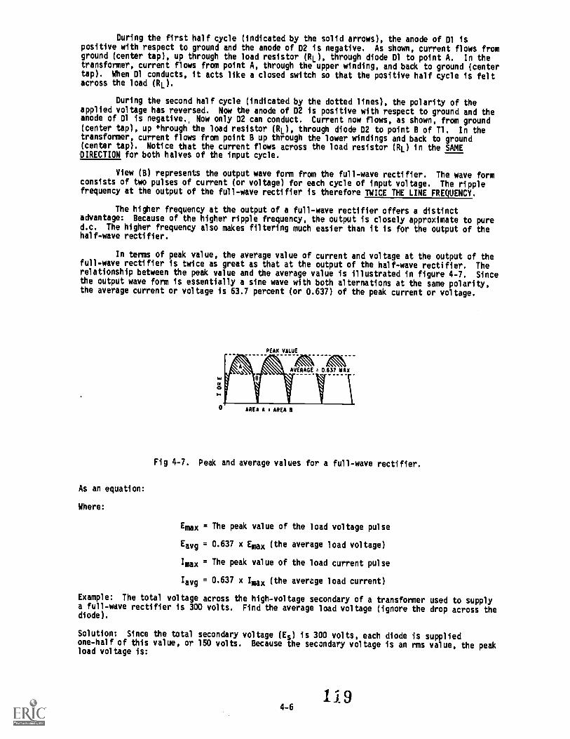
During the first half cycle (indicated by the solid arrows), the anode of 01 ispositive with respect to ground and the anode of D2 is negative. As shown, current flows fromground (center tap), up through the load resistor (RL), through diode 01 to point A. In thetransformer, current flows from point A, through the upper winding, and back to ground (centertap). When 01 conducts, it acts like a closed switch so that the positive half cycle is feltacross the load (RL).
During the second half cycle (indicated by the dotted lines), the polarity of theapplied voltage has reversed. Now the anode of D2 is positive with respect to ground and theanode of 01 is negative. Now only D2 can conduct. Current now flows, as shown, from ground(center tap), up through the load resistor (RL), through diode D2 to point B of Tl. In thetransformer, current flows from point B up through the lower windings and back to ground(center tap). Notice that the current flows across the load resistor (RL) in the SAMEDIRECTION for both halves of the input cycle.
View (B) represents the output wave form from the full-wave rectifier. The wave formconsists of two pulses of current (or voltage) for each cycle of input voltage. The ripplefrequency at the output of the full-wave rectifier is therefore TWICE THE LINE FREQUENCY.
The higher frequency at the output of a full-wave rectifier offers a distinctadvantage: Because of the higher ripple frequency, the output is closely approximate to pured.c. The higher frequency also makes filtering much easier than it is for the output of thehalf-wave rectifier.
In terms of peak value, the average value of current and voltage at the output of thefull-wave rectifier is twice as great as that at the output of the half-wave rectifier. Therelationship between the peak value and the average value is illustrated in figure 4-7. Sincethe output wave form is essentially a sine wave with both alternations at the same polarity,the average current or voltage is 63.7 percent (or 0.637) of the peak current or voltage.
PEAK VALUE
Fig 4-7. Peak and average values for a full-wave rectifier.
As an equation:
Where:
Emax = The peak value of the load voltage pulse
Eavg = 0.637 x Emax (the average load voltage)
Imax = The peak value of the load current pulse
Iavg = 0.637 x Imax (the average load current)
Example: The total voltage across the high-voltage secondary of a transformera full-wave rectifier is 300 volts. Find the average load voltage (ignore thediode).
Solution: Since the total secondary voltage (Es) is 300 volts, each diode isone-half of this value, or 150 volts. Because the secondary voltage is an rmsload voltage is:
1194-6
used to supplydrop across the
suppliedvalue, the peak

Emax = 1.414 x Es
Emax = 1.414 x 150
Emax 2 212 volts
The average load voltage is:
Eavg . 0.637 x Emax
Eavg I 0.637 x 212
135 voltsEavg 2
Note: If you have problems with this equation, review the portion of FM 11-61(Communications-Llectronics Fundamentals: Basic Principles of AlternatingCurrent) that pertains to this subject.
As you may recall from your past studies in electricity, every circuit has advantagesand disadvantages. The full-wave rectifier is no exception. In studying the full-waverectifier, you may have found that by doubling the output frequency, the average voltage hasdoubled, and the resulting signal is much easier to filter because of the high ripplefrequency. The only disadvantage is that the peak voltage in the full-wave rectifier is onlyhalf the peak voltage in the half-wave rectifier. This is because the secondary of the powertransformer in the full-wave rectifier is center tapped; therefore, only half the sourcevoltage goes to each diode.
Fortunately, there is a rectifier which produces the same peak voltage as a half-waverectifier and the same ripple frequency as a full-wave rectifier. This circuit, known as theBRIDGE RECTIFIER, will be the subject of our next discussion.
The bridge rectifier. When four diodes are connected as shown in figure 4-8, thecircuit is callea a BRIDGE RECTIFIER. The input to the circuit is applied to the diagonallyopposite corners of the network, and the output is taken from the remaining two corners.
&AD
Fig 4-8. Bridge rectifier.
One complete cycle of operation will be discussed to help you understand how thiscircuit works. Let us assume the transformer is working properly and there is a positivepotential at point A and a negative potential at point B. The positive potential at point Awill forward bias D3 and reverse bias D4. The negative potential at point B will forward biasD1 and reverse bias D2. At this time D3 and D1 are forward biased and will allow current flowto pass through them; D4 and D2 are reverse biased and will block current flow. The path forcurrent flow is from point B through D1, up through RL, through D3, through the secondary ofthe transformer back to point B. This path is indicated by the solid arrows. Wave forms (1)and (2) can be observed across D1 and D3.

One-half cycle later the polarity across the secondary of the transformer reverses,forward biasing 02 and 04 and reverse biasing 01 and 03. Current flow will now be from pqintA through 04, up through RL, through 02, through the secondary of Tl, and back to point A.This path is indicated by the broken arrows. Waveforms (3) and (4) can be observed across 02and 04. You should have noted that the current flow through RL is always in the samedirection. In flowing through RL this current develops a voltage corresponding to thatshown in waveforms (5). Since current flows through the load (RL) during both half cyclesof the applied voltage, this bridge rectifier is a full-wave rectifier.
One advantage of a bridge rectifier over a conventional full-wave rectifier is thatwith a given transformer the bridge rectifier produces a voltage output that is nearly twicethat of the conventional full-wave circuit. This may be shown by assigning values to some ofthe components shown in views (A) and (B) of figure 4-9. Assume that the same transformer isused in both circuits. The peak voltage developed between points X and Y is 1000 volts inboth circuits. In the conventional fullwave circuit shown in view (A), the peak voltage fromthe center tap to either X or Y is 500 volts. Since only one diode can conduct at anyinstant, the maximum voltage that can be rectified at any instant is 500 volts. Therefore,the maximum voltage that appears across the load resistor is nearly - but never exceeds - 500volts, as a result of the small voltage drop across the diode. In the bridge rectifier shownin view (B), the maximum voltage that can be rectified is the full secondary voltage, which is1000 volts. Therefore, the peak output voltage across the load resistor is nearly 1000volts. With both circuits using the same transformer, the bridge rectifier circuit produces ahigher output voltage than the conventional full-wave rectifier circuit.
(A)
T1
(8)
A. Conventional full-wave rectifierB. Full-wave bridge rectifier
Fig 4-9. Comparison of a conventional and bridge full-wave rectifier.
FILTERS
While the output of a rectifier is a pulsating d.c., most electronic circuits requirea substantially pure d.c. for proper operation. This type of output is provided by SINGLE ormultisection filter circuits placed between the output of the rectifier and the load.
There are four basic types of fllter circuits:
Simple capacitor filter
LC choke-input filter

LC capacitor-input filter (pi-type)
RC capacitor-input filter (pi-type)
The function of each of these filters will be covered in detail.
Filtering is accomplished by the use of capacitors, inductors, and/or resistors invarious combinations. Inductors are used as series impedance to oppose the flow ofalternating (pulsating d.c.) current. Capacitors are used as shunt elements to bypass thealternating components of the signal around the load (to ground). Resistors are used in placeof inductors in low current applications.
Let's briefly review the properties of a capacitor. First, a capacitor opposes anychange in voltage. The opposition to a change is voltage is called capacitive reactance(Xc) and is measured in ohms. The capacitive reactance is determined by the frequency (f)of ihe applied voltage and the capacitance (C) of the capacitor.
Xc . 1 or .159
From this formula, you can see that if frequency or capacitance is increased, the Xcdecreases. Since filter capacitors are placed in parallel with the load, a low Xc willprovide better filtering than a high Xc. For this to be accomplished, a better shuntingeffect of the a.c. around the load is provided, as shown in figure 4-10.
To obtain a steady d. c. output, the capacitor must charge almost instantaneously tothe value of applied voltage. Once charged, the capacitor must retain the charge as long aspossible. The capacitor must have a short charge time constant (view A). This can beaccomplished by keeping the internal resistance of the power supply as small as possible (fastcharge time) and the resistance of the load as large as possible (for a slow discharge time asillustrated in view 8.).
I ROWER
SUPPLY
CHARGE /
t
( A )
ROWERSUPPLY
LOAD
A. Fast chargeB. Slow discharge
IrnI[DISCHARGE,
PATH ......
LOAD
(B)
Fig 4-10. Capacitor filter.
From your earlier studies in basic electricity, you may remember that one timeconstant is defined as the time it takes a capacitor to charge to 63.2 percent of.the appliedvoltage or to discharge to 36.8 percent of its total charge. This action can be expressed bythe following equation:
t RC
R represents the resistance to the charge or discharge path
And:
C represents the capacitance of the capacitor.
You should also recall that a capacitor is considered fully charged after five RC timeconstants. Refer to figure 4-11. You can see that a steady d.c. output voltage is obtainedwhen the capacitor charges rapidly and discharges as slowly as possible.
Where:
4-9 1 2 2

In filter circuits, the capecitor is the common element to both the charge and thedIscherge paths. Therefore, to obtain the longest possible discharge time, you want thecapecitir le be as large es possible. Another way to look at it is: The capacitor acts as ashort circuit around lie load (es far as the a.c. component is concerned), and since thelime the Oahe Of the capecitor (C), the muller the opposition (Xc) or resistance to a.c.
1Ic* zvNew let's leek at intectors end their application in filter circuits. Remember, AN
alraltilitrprigrirtirlaillrrIINT. In case you have forgotten, a change in currentg electromagnetic field. The changing field, in turn,
cite the ulmdlegs of the wire in the inductor and thereby proem's a counterelectromotivefora IcsoN1. It Is VAS cot that opposes the change in circuit current. Opposition to achamp In cermet st a given P equncy is called inductive reactance (XL) and is measured inOhms. The indective reactance ( L) of an indictor is determined by the applied frequencySid 100 Inductance of the indicter.
Nethemetically,
XL 2 w ft
If frequeecy er indictance is increased, the XL increases. Since inductors are placed inseries with the lad (as shown in figure 4-12), the larger the XL, the larger the a.c.voltage developed across the Iced.
New refer te figure 4-13. When the current starts te flow through the coil, anmandleg seenetic field builds up around the inductor. This magnetic field around the coil&veep the cemf that opposes the change in current, then the rectifier current decreases,as ahem In figure 4-14, the mimetic field collapses and again cuts the turns (windings) ofwire, thus iodides current into the coil. This additional current merges with the rectifiertorrent snd attempts tete, it at its original level.
New that yee have read hew the components in a filter circuit react to current flowtree the rectifier, the different types of filter circuits in use todAy will be discussed.
.123
4-10

100
0
SO
10
AO
AO
ovum wits DISCHA1/09
SO100
ILl
10
INC MC 511C 41C 511C 1
Time
Fig 4-11. RC time constant.
LANGE ACVOLTAGE NOP
NALL ACvOLTAAE ONOP
4
Fig 4-12. Voltage drops in an inductive filter.
4-11 12 4

EXPANDING
L I.1MAGNETIC
FIELD.Fig 4-13. Inductive filter (expanding field).
The capacitor filter. The simple capacitor filter is the most basic type of powersupply filter. The application of the simple capacitor filter is very limited. It issometimes used on extremely high-voltage, low-current power supplies for cathode-ray andsimilar electron tubes which require very little load current from the supply. The capacitorf11ttr is also used where the power-supply ripple frequency is not critical; this frequencycan be relatively high. The capacitor (C1) shown in figure 4-15 is a simple filter connectedacross the output of the rectifier in parallel with the load.
POIVENSUPPLY
COLLAPSINGMAGNETIC
I FIELD
f INDUCED.. CURRENT
Fig 4-14. Inductive filter (collapsing field).
Tl
III
DI
Fig 4-15. Full-wave rectifier with a capacitor filter.
When this filter is used, the RC charge time of the filter capacitor (C1) must beshort and the RC discharge time must be long to eliminate ripple action. In other words, thecapacitor must charge up fast, preferably with no discharge at all. Better filtering alsoresults when the input frequency is high; therefore, the full-wave rectifier output is easierto filter than that of the half.vave rectifier because of its higher frequency.
For you to have a better understanding of the effect that filtering has on Eava, acomparison of a rectifier circuit with a filter and one without a filter is illustrated inviews (A) and (B) of figure 4-16. The output waveforms in figure 4-16 represent theunfiltered and filtered outputs of the halfwave rectifier circuit. Current pulses flowthrough the load resistance (RL) each time a diode conducts. The dashed line indicates theaverage value of output voltage. For the half-wave rectifier, Eava is less than half (orapproximately 0.318) of the peak output voltage. This value is stfll much less than that ofthe applied voltage. With no capacitor connected across the output of the rectifier circuit,the waveform in view (A) has a large pulsating component (ripple) compared with the averageor d.c. component. When a capacitor is connected across the output (view B), the averagevalue of output voltage (Eavg) is increased due to the filtering action of capacitor Cl.
4-12125

(A)
TI DI
(B)
A. UnfilteredB. Filtered
ICYCLE
RL Eavq
.410/
ErEavg
Fig 4-16. Half-wave rectifier with and without filtering.
The value of the capacitor is fairly large (several microfarads), thus it presents arelatively low reactance to the pulsating current and it stores a substantial charge. The
rate of charge for the capacitor is limited only by the resistance of the conducting diodewhich is relatively low. Therefore, the RC .iharge time of the circuit is relatively short.As a result, when the pulsating voltage is f rs applied to the circuit, the capacitor chargesrapidly and almost reaches the peak value of the rectified voltage within the first fewcycles. The capacitor attempts to charge to the peak value of the rectified voltage anytime adiode is conducting, and tends to retain its charge when the rectifier output falls to zero.(The capacitor cannot discharge immediately.) The capacitor slowly discharges through theload resistance (RL) during the time the rectifier is nonconducting.
The rate of discharge of the capacitor is determined by the value of capacitance andthe value of the load resistance. If the capacitance and load-resistance values are large,the RC discharge time for the circuit is relatively long.
A comparison of the wave forms shown in figure 4-16 illustrates that the addition ofCl to the circuit results in an increase in the average of the output voltage (Eava) and areduction in the amplitude of the ripple component (Er) which is normally present across theload resistance.
Now, let's consider a complete cycle of operation using a half-wave rectifier, acapacitive filter (C1), and a load resistor (RL). As shown in view (A) of figure 4-17, thecapacitive filter (C1) is assumed to be large enough to ensure a small reactance to thepulsating rectified current. The resistance of RL is assumed to be much greater than thereactance of Cl at the input frequency. When the circuit is energized, the diode conducts onthe positive half cycle and current flows through the circuit, allowing Cl to charge. Cl willcharge to approximately the peak value of the input voltage. (The charge is less than thepeak value because of the voltage drop across the diode (D1)). In view (A) of the figure, thecharge on Cl is indicated by the heavy solid line on the wave form. As illustrated in view(8),'the diode cannot conduct on the negative half cycle because the anode of D1 is negativein respect to the cathode. During this interval, Cl discharges through the load resistor(RL). The discharge of Cl produces the downward slope as indicated by the solid line on thewave form in view (B). In contrast to the abrupt fall of the applied a.c. voltage from peakvalue to zero, the voltage across Cl (and thus across RL) during the discharge periodgradually decreases until the time of the next half cycTe of rectifier operation. Keep inmind that for good filtering, the filter capacitor should charge up as fast as possible anddischarge as little as possible.

9i1
DI
(A)
DI
(B)
CAPACITORCHARGE
CAPACITORDISCHARGE
A. Positive half-cycleB. Negative half-cycle
WONT OFDISCHARGE
Fig 4-17. Capacitor filter circuit (positive and negative half cycles).
Since practical values of Cl and RL ensure a more or less gradual decrease of thedischarge voltage, a substantial charge maintains on the capacitor at the time of the nexthalf cycle of operation. As a result, no current can flow through the diode until the risinga.c. input voltage at the anode of the diode exceeds the voltage of the charge remaining onCl. The charge on Cl is the cathode potential of the diode. When the potential on the anodeexceeds the potential on the cathode (the charge on C1), the diode again conducts, and Clbegins to charge to approximately the peak value of the applied voltage.
Fig 4-18. Full-wave rectifier (with capacitor filter).
After the capacitor has charged to its peak value, the diode will cut off and thecapacitor will start to discharge. Since the fall of the a.c. input voltage on the anode isconsiderably more rapid than the decrease on the capacitor voltage, the cathode quicklybecomes more positive than the anode, and the diode ceases to conduct.
Operation of the simple capacitor filter using a full-wave rectifier is basically thesame as that discussed for the half-wave rectifier. Referring to figure 4-18, you shouldnotice that because one of the diodes is always conducting on either alternation, the filtercapacitor charges and discharges during each half cycle. (Note that each diode conducts onlyfor that portion of time when the peak secondary voltage is greater than the charge across thecapacitor.)
Another thing to keep in mind is that the ripple component (Er) of the outputvoltage is an a.c. voltage and the average output voltage (Eava) is the d.c. component ofthe output. Since the filter capacitor offers a relatively Tog impedance to a.c., themajority of the a.c. component flows through the filter capacitor. The a.c. component is,therefore, bypassed (shunted) around the load resistance, and the entire d.c. component (orEan) flows through the load resistance. This statement can be clarified by using thefo ula for X,c in a half-wave and full-wave rectifier. First, you must establish somevalues for the circuit.

HALF-WAVE RECTIFIER
FREQUENCY AT RECTIFIER
OUTPUT: 60 Pz
VALUE OF FILTER CAPACITOR:
FULL-WAVE RECTIFIER
FREQUENCY AT RECTIFIER
OUTPUT: 120 Hz
VALUE OF FILTER CAPACITOR:
3Cp F
LOAD RESISTANCE (RL):
30. F
10 k0 LOAD RESISTANCE (RL): 10 k
1 1
Xc -2FTC-7 XC = -7777-fC
Xc.159
--fc-- Xc 0.159
--Tr--
.159 .159
Xc = 60 x .000030 Xc 120 x .000030
.159 .159
Xc = -70018 Xc = -7036-
Xc = 88.30 Xc = 44.160
As you can see from the calculations, by doubling the frequency of the rectifier, youreduce the impedance of the capacitor by one-half. This allows the a.c. component to pass
through the capacitor more easily. As a result, a full-wave rectifier output is much easier
to filter than that of a half-wave rectifier. Remember, the smaller the Xc of the filter
capacitor in respect to the load resistance, the better the filtering action since the largest
possible capacitor will provide the best filtering. Remember, also, that the load resistance
is an important consideration. If load resistance is made small, the load current increases,
and the average value of output voltage (Eava) decreases. The RC discharge time constant isa direct function of the value of the load resistance; therefore, tne rate of capacitor
voltage discharge is a direct function of the current through the load. The greater load
current, the more rapid the discharge of the capacitor, and the lower the average value of
output voltage. For this reason, the simple capacitive filter is seldom used with rectifier
circuits that must supply a relatively large load current. Using the simple capacitive filter
in conjunction with a full-wave or bridge rectifier provides improved filtering because theincreased ripple frequency decreases the capacitive reactance of the filter capacitor.
1
Xc = 2 it fC
The LC CHOKE-INPUT FILTER is used primarily in power supplies where voltage regulationis important and where the output current is relatively high and subject to varying load
conditions. The filter is used in high power applications such as those found in radars and
communication transmitters.
Notice in figure 4-19 that this filter consists of an input inductor (L1), or filter
choke, and an output filter capacitor (C1). IndUctor Ll is placed at the input to the filter
and is in series with the output of the rectifier circuit. Since the action of an inductor is
to oppose any change in current flow, the inductor tends to keep a constant current flowing to
the load throughout the complete cycle of the applied voltage. As a result, the output
voltage never reaches the peak value of the applied voltage. Instead, the output voltage
approximates the average value of the rectified input to the filter, as shown in the figure.The reactance of the inductor (XL) reduces the amplitude of ripple voltage without reducing
the d.c. output voltage by an appreciable amount. (The d.c. resistance of the inductor is
just a few ohms.)

Eave Er
:Thl:Z-"SM7-"S7:SJ;.)
Fig 4-19. LC choke-input filter.
The shunt capacitor (C1) charges and discharges at the ripple frequency rate, but theamplitude of the ripple voltage (Er) is relatively small because the inductor (L1) tends tokeep a constant current flowing from the rectifier circuit to the load. In addition, thereactance of the shunt capacitor (Xc) presents a low impedance to the ripple componentexisting at the output of the filter, and thus shunts the ripple component around the load.The capacitor attempts to hold the output voltage relatively constant at the average value ofthe voltage.
The value of the filter capacitor (C1) must be relatively large to present a lowopposition (Xc) to the pulsating current and to store a substantial charge. The rate of thecharge for the capacitor is limited by the low impedance of the a.c. source (the transformer),the small resistance of the diode, and the counterelectromotive force (cemf) developed by thecoil. Therefore, the RC charge time constant is short compared to its discharge time. (Thiscomparison in RC charge and discharge paths is illustrated in views (A) and (B) of figure4-20.) Consequently, when the pulsating voltage is first applied to the LC choke-inputfilter, the inductor (L1) produces a cemf which opposes the constantly increasing inputvoltage. The net result is to prevent effectively the rapid charging of the filter capacitor(C1). Thus, instead of reaching the peak value of the input voltage, Cl only charges to theaverage value of the input voltage. After the input voltage reaches its peak and decreasessufficiently, the capacitor (C1) attempts to discharge through the load resistance (RL). Clwill only partially discharge, as indicated in view (B) of the figure, because of itsrelatively long discharge time constant. The larger the value of the filter capacitor, thebetter the filtering action. However, because of physical size, there is a practicallimitation to the maximum value of the capacitor.
1 r) Oh44-16

L I
( A )
LI
A. Charge PathB. Discharge Palh
Fig 4-20. LC choke-input filter (charge and discharge paths).
The inductor (also referred to as the filter choke or coil) serves to maintain thecurrent flow to the filter output (k) at a nearly constant level during the charge anddischarge periods of the filter capacitor. The inductor (1.1) and the capacitor (C1) form avoltage divider for the a.c. component (ripple) of the applied input voltage. This is shownin views (A) and (B) of figure 4-21. As far as the ripple component is concerned, theinductor offers a high impedance (Z) and the capacitor offers a low impedance (view B). As aresult, the ripple component (Er) appearing across the load resistance is greatly attenuated(reduced). The inductance of the filter choke opposes change in the value of the currentflowing through it; therefore, the average value of the voltage produced across the capacitorcontains a much smaller value of ripple component (Er) than the value of ripple producedacross the choke.
L I
(A)
A.C.COMPONENT
JIILiNIGN
IMPEOENCE
(B)
A. LC choke-lapel fillerB. IFAluivIdent circuit
LOWimeEDENCE
Fig 4-21. LC choke-input filter.

Fig 4-22. Filtering action of the LC choke-input filter.
Now look at figure 4-22 which illustrates a complete cycle of operation for afull-wave rectifier circuit used to supply the input voltage to the filter. The rectifiervoltage is developed across the capacitor (C1). The ripple voltage at the output of thefilter is the alternating component of the input voltage reduced in amplitude by the filtersection. Each time the anode of a diode goes positive with respect to the cathode, the diodeconducts the CI charges. Conduction occurs twice during each cycle for a full-waverectifier. For a 60-hertz supply, this produces a 120-hertz ripple voltage. Although thediodes alternate (one conducts while the other is nonconducting), the filter input voltage isnot steady. As the anode voltage of the conducting diode increases (on the positive half ofthe cycle), capacitor CI charges - the charge being limited by the impedance of the secondarytransformer winding, the diode's forward (cathode-to-anode) resistance, and thecounterelectromotive force developed by the choke. During the nonconducting interval (whenthe anode voltage drops below the capacitor charge voltage), CI discharges through the loadresistor (k). The components in the discharge path have a long time constant; thus, CIdischarges more slowly than it charges.
The choke (L1) is usually a large value, from 1 to 20 henries, and offers a largeinductive reactance to the 120-hertz ripple component produced by the rectifier. Therefore,the effect that LI has on the charging of the capacitor (C1) must be considered. Since LI isconnected in series with the parallel branch consisting of CI and RI., a division of theripple (a.c.) voltage and the output (d.c.) voltage occurs. The greater the impedance of thechoke, the less the ripple voltage that appears across CI and the output. The d.c. outputvoltage is fixed mainly by the d.c. resistance of the choke.
Now that you have read how the LC choke-input filter functions, it will be discussedwith actual component values applied. For simplicity, the input frequency at the primary ofthe transformer will be 117 volts 60 hertz. Both half-wave and full-wave rectifier circuitswill be used to provide the input to the filter.
101ift
Fig 4-23. Half-wave rectifier with an LC choke-input filter.
Starting with the half-wave configuration shown in figure 4-23, the basic parametersare: With 117 volts a.c. rms applied to the 11 primary, 165 volts a.c. peak-to-peak isavailable at the secondary [(117 V) x (1.414) = 165 V]. You should recall that the ripplefrequency of this half-wave rectifier is 60 hertz. Therefore, the capacitive reactance of Clis:

1
Xc= 2 '7( fC
Xc = 1
(2) (3.14) (60) (10) (10-6)
(1) (10.6)
Xc m 3768
Xc = 265 ohms
This means that the capacitor (C1) offers 265 ohms of opposition to the ripple current. Note,
however, that the capacitor offers an infinite impedance to direct current. The inductivereactance of Ll is:
XL =
XL = (2) (3.14) (60) (10)
XL = 3.8 kilohms
The above calculation shows that Ll offers a relatively high opposition (3.8 kilohms) to theripple in comparison to the opposition offered by Cl (265 ohms). Thus, more ripple voltagewill be dropped across Ll than across Cl. In addition, the impedance of Cl (265 ohms) isrelatively low in respect to the resistance of the load (10 kilohms). Therefore, more ripplecurrent flows through Cl than the load. In other words, Cl shunts most of the a.c. componentaround the load.
xL13.(11i
LI II
LIX L 3 On
11
I S10111XC s2115ft-
-(A) ( B
A. LC ehoke-input filterB. Equivalent circuit
Fig 4-24. A.c. component in an LC choke-input filter.
Let's go a step further and redraw the filter circuit so that you can see the voltagedivider action. Refer to view (A) of figure 4-24. Remember, the 165 volts peak-to-peak 60hertz provided by the rectifier consists of both an a.c. and a d.c. component. This firstdiscussion will be about the a.c. component. From the figure, you see that the capacitor (C1)offers the least opposition (265 ohms) to the a.c. component; therefore, the greatest amountof a.c. will flow through Cl. (The heavy line indicates the a.c. current flow through the
capacitor.) Thus, the capacitor bypasses, or shunts, most of the a.c. around the load.
By combining the Xc of Cl and the resistance of RL into an equivalent circuit(view B), you will have a total resistance of 258 ohms.
As a formula:
RT (R1) (R2)
RI + R2
You now have a voltage divider as illustrated in figure 4-25. You should see that because ofthe impedance ratios, a large amount of ripple voltage is dropped across Ll, and asubstantially smaller amount is dropped across Cl and 'IL. You can further increase theripple voltage across Li by increasing the inductance (XL = 245(fL).
4-19
132

CI
11
LI I LARGE
XL. SIM RIPPLE it 3.11k4VOLTAGE
SMALLRIPPLE
El 2511f1VOLTAGE
Fig 4-25. Equivalent circuit of an LC choke-input filter.
Now let's discuss the d.c. component of the applied voltage. Remember, a capacitoroffers an infinite (CO) impedance to the flow of direct current. The d.c. component,therefore, must flow through RL and Ll. As far as the d.c. is concerned, the capacitor doesnot exist. The coil and the load are, thererore, in series with each other. The d.c.resistance of a filter choke is very low (50 ohms average). Consequently, most of the d.c.component is developed across the load and a very small amount of the d.c. voltage is droppedacross the coil, as shown in figure 4-26.
Ill! (SOA NOMINAL)
D.C. COMPONENT
Fig 4-26. D.C. component in an LC choke-input filter.
Fig 4-27. Full-wave rectifier with an LC choke-input filter.
As you may have noticed, both the a.c. and the d.c. components flow through Ll.Because it is frequency sensitive, the coil provides a large resistance to a.c. and a smallresistance to d.c. In other words, the coil opposes any change in current. This propertymakes the cu, a highly desirable filter component. Note that the filtering action of the LCchoke-input filter is improved when the filter is used in conjunction with a full-waverectifier, as shown in figure 4-27. This is due to the decrease in the Xc of the. filtercapacitor and the increase in the XL of the choke. Remember, ripple frequency of afull-wave rectifier is twice that of a half-wave rectifier. For a 60-hertz input, the ripplewill be 120 hertz. The Xc of Cl and the XL of Ll is calculated as follows:
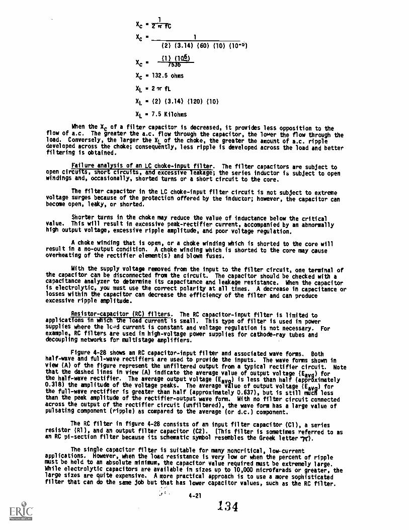
xc n7Ttxc 1
(2) (3.14) (60) (10) (10-0)
(1) (10.6.)Xc MI6
Xc 132.5 ohms
XL 2irr fL
XL (2) (3.14) (120) (10)
XL 7.5 Kilohms
When the Xc of a filter capacitor is decreased, it provides less opposition to theflow of a.c. The greater the a.c. flow through the capacitor, the lower the flow through theload. Conversely, the larger the XL of the choke, the greater the amount of a.c. rippledeveloped across the choke; consequently, less ripple is developed across the load and betterfiltering is dbtained.
Failure analysis of an LC choke-input filter. The filter capacitors are subject toopen circuits, short circuits, and excessive leakage; the series indUctor .6 subject to openwindings and, occasionally, shorted turns or a short circuit to the core.
The filter capacitor in the LC choke-input filter circuit is not subject to extremevoltage surges because of the protection offered by the inductor; however, the capacitor canbecome open, leaky, or shorted.
Shorter turns in the choke may reduce the value of inductance below the criticalvalue. This will result in excessive peak-rectifier current, accompanied by an abnormallyhigh output voltage, excessive ripple amplitude, and poor voltage regulation.
A choke winding that is open, or a choke winding which is shorted to the core willresult in a no-output condition. A choke winding which is shorted to the core may causeoverheating of the rectifier element(s) and blown fuses.
With the supply voltage removed from the input to the filter circuit, one terminal ofthe capacitor can be disconnected from the circuit. The capacitor should be checked with acapacitance analyzer to determine its capacitance and leakage resistance. When the capacitoris electrolytic, you must use the correct polarity at all times. A decrease in capacitance orlosses within the capacitor can decrease the efficiency of the filter and can produceexcessive ripple amplitude.
Resistor-capacitor (RC) filters. The RC capacitor-input filter is limited toapplications in which the load current is small. This type of filter is used in powersupplies where the 1c4d current is constant and voltage regulation is not necessary. Forexample, RC filters are used in high-voltage power supplies for cathode-ray tubes anddecoupling networks for multistage amplifiers.
Figure 4-28 shows an RC capacitor-input filter and associated wave forms. Bothhalf-wave and full-wave rectifiers are used to provide the inputs. The wave forms shown inview (A) of the figure represent the unfiltered output from a typical rectifier circuit. Notethat the dashed lines in view (A) indicate the average value of output voltage (Eava) forthe half-wave rectifier. The average output voltage (Eava) is less than half (approximately0.318) the amplitude of the voltage peaks. The average vilue of output voltage (Eava) forthe full-wave rectifier is greater than half (approximately 0.637), but is still mudi lessthan the peak amplitude of the rectifier-output wave form. With no filter circuit connectedacross the output of the rectifier circuit (unfiltered), the wave form has a large value ofpulsating component (ripple) as compared to the average (or d.c.) component.
The RC filter in figure 4-28 consists of an input filter capacitor (C1), a seriesresistor (R1), and an output filter capacitor (C2). (This filter is sometimes referred to asan RC pi-section filter because its schematic symbol resembles the Greek letter 111.
The single capacitor filter is suitable for many noncritical, low.currentapplications. However, when the load resistance is very low or when the percent of ripplemust be held to an absolute minimum, the capacitor value required must be extremely large.While electrolytic capacitors are available in sizes up to 10,000 microfarads or greater, thelarge sizes are quite expensive. A more practical approach is to use a more sophisticatedfilter that can do the same job but that has lower capacitor values, such as the RC filter.
4-21
1) 4

1CYCLE
INPUTFROol CIRECTIFIER
R I
=M.
PEAK
0.318V PEAK LErEl:Ng TEovg
HALF -WAVE RECTIFIER
OUTPUT(LOAD)
C2 RL
Er
Eovg
PEAK 27:FZ-1-41"---1---Er--...-c.-24---11:10:17vg Eavg ECM'
FULL-WAVE RECTIFIER
(A) ( B) ( C )
A. Unfiltered output voltage from rectifierB. Voltage acrou capacitor CIC. Voltage acrou capacitor C2
Fig 4-28. RC filter and waveforms.
Views (A), (B), and (C) of figure 4-28 show the output wave forms of a half-wave andfull-wave rectifier. Each wave form is shown with an RC filter connected across the output.The following explanation of how a filter works will show you than an RC filter of this typedoes a much better job than the single capacitor filter.
Cl performs exactly the same function as it did in the single capacitor filter. It isused to reduce the percentage of ripple to a relatively low value. Thus, the voltage acrossCl might consist of an average d.c. value of +100 volts with a ripple voltage of 10 voltspeak-to-peak. This voltage is passed on to the R1-C2 network, which reduces the ripple evenfurther.
C2 offers an infintte impedance (resistance) to the d.c. component of the outputvoltage. Thus, the d.c. voltage is passed to the load, but reduced in value by the amount ofthe voltage drop across Rl. However, R1 is generally small compared to the load resistance.Therefore, the drop in the d.c. voltage by R1 is not a drawback.
Component values are designed so that the resistance of R1 is much greater than thereactance (Xc) of C2 at the ripple frequency. C2 offers a very low impedance to the a.c.ripple frequency. Thus, the a.c. rippls senses a voltage divider consisting of R1 and C2between the output of the rectifier and ground. Therefore, most of the ripple voltage isdropped across Rl. Only a trace of the ripple voltage can be seen across C2 and the load. Inextreme cases where the r'pple must be held to an absolute minimum, a second stage of RCfiltering can be added. in gractice, the second stage is rarely required. The RC filter isextremely popular becau.( smc:ler capacitors can be used with good results.
The RC filter ha; s 4isadvantages. First, the voltage drop across R1 takes voltageLowy from the load. 3e,:-..nd ?i er is wasted in RI and is dissipated in the form of unwantedheat. Finally, if thl 4ad -lstance changes, the voltage across the load will change. Evenso, the advantages oi t R, :ilter overshadow these disadvantages in many cases.
Failure analysis of the resistor-capacitor (RC) filter. The shunt capacitors (C1 andC2) are subject to an open circuit, a short circuit, or excessive leakage. The series filterresistor (R1) is subject to changes in value and occasionally opens. Any of these troublescan be easily detected.
14'6.42 Auk

The input capacitor (C1) has the greatest pulsating voltage applied to it and is themost susceptible to voltage surges. As a result, the input capacitor is frequently subject tovoltage breakdown and shorting. The remaining shunt capacitor (C2) in the filter circuit isnot subject to voltage surges because of the protection offered by the series filter resistor(R1). However, a shunt capacitor can become open, leaky, or shorted.
A shorted capacitor or an open filter resistor results in a no-output indication. Anopen filter resistor results in an abnormally high d.c. voltage at the input to the filter andno voltage at the output of the filter. Leaky capacitors or filter resistors that have losttheir effectiveness, or filter resistors that have decreased in value, result in an excessiveripple amplitude in the output of the supply.
The LC CAPACITOR-INPUT FILTER is one of the most commonly used filters. This type offilter is used primarily in radio receivers, small audio amplifier power supplies, and in anytype of power supply where the output current is low and the load current is relativelyconstant.
Figure 4-29 shows an LC capacitor-input filter and associated wave forms. Bothhalf-wave and full-wave rectifier circuits are used to provide the input. The wave formsshown in view (A) of the figure represent the unfiltered output from a typical rectifiercircuit. Note that the average value of output voltage (Eava), indicated by the dashedlines, for the half-wave rectifier is less than half the ampTitude of the voltage peaks. Theaverage value of output voltage (Eava) for the full-wave rectifier is greater than half, butis still much less than the pLk amplitude of the rectifier-output waveform. With no filterconnected across the output blthe rectifier circuit (which results in unfiltered outputvoltage), the wave form has a large value of pulsating component (ripple) as compared to theaverage (or d.c.) component.
Cl reduces the ripple to a relatively low level (view B). Ll and C2 form the LCfilter which reduces the ripple even further. Ll is a large value iron-core inductor(choke). LI has a high value of inductance and, therefore, a high value of XL which offersa high reactance to the ripple frequency. At the same time, C2 offers a very low reactance toa.c. ripple. Ll and C2 form an a.c. voltage divider and, because the reactance of LI is muchhigher than that of C2, most of the ripple voltage is dropped across LI. Only a slight traceof ripple appears across C2 and the load (view C).
While the LI-C2 network greatly reduces a.c. ripple, it has little effect on d.c.ripple. You should recall that an inductor offers no reactance to d.c. The only oppositionto current flow is the resistance of the wire in the choke. Generally, this resistance isvery low and the d.c. voltage drop across the coil is minimal. Thus, the LC filter overcomesthe disadvantages of the RC filter.
LI
INPUTO--rYVYN-0--
CI TC2
PEAK
0.318V PEAK
HALF-WAVE RECTIFIER
OUTPUT
EavgT
_y PEAK .7Q. Er c'tic _EEmig avg Eavg
FULL-WAVE RECTIFIER
(A) (B) ( C)
A. Unfiltered output voltage from rectifier B. Voltage across capacitor CI
Fig 4-29. LC filter and waveforms.
443 1.36
C. Voltage acrou capacitor C2

Aside fro the voltage divider effect, the inductor improves filtering in anotherway. Tee shield mall that es indicter resists changes in the monitude of the currentflowing three. it. Coselesstly, when the inductor is placed in series with the load, theloducter maintains stody carrot. In turn, this helps the voltage across the load remaincanton who the size of the components is a factor.
Me LC filter provides good filtering action over a wide range of currents. ThetePeCiter filters best ekes the load is drawing little current. Thus, the capacitordiscbarges very slowly asd the output voltage remains almost constant. On the other hand, theindecter filters best who the corset is highest. The complementary nature of these twoc000mts enures that good filtering will occur over a wide range of currents.
The LC filter has two disadvantages. First, it is more expensive than the RC filterOcoee en iren-cere choke costs more than a resistor. The second disadvantage is size. Thetree-ore ceeke is balky sad heavy, a fact which may render the LC filter unsuitable for manyapplicetiess.
f 1 r. Shunt capacitors are subject toedee ci es Inductors are subject to openeindings asd occasionally shorted terns or a short circuit to the core.
The lost capacitor 101, which has the greatest pulsating voltage applied to it, isthe mot soceptIble te voltage urges, and has a generally higher average voltage applied.As a melt, the inpet coulter is frequently subject to voltage breakdown and shorting. TheMot capacitor ICIl is not as susceptible to voltage surges because of the series protectionoffered by the series indector (LI), bet the capacitor can become open, leaky, or shorted.
A shorted capacitor, an open filter choke, or a choke wtnding which is shorted to thecore, melts la a weetput indication. A shorted capacitor, depending on the magnitude ofthe shert, ley coo a shorted rectifier, transformer, or filter choke, and eay result in ablown foe in the primary of the transferor. An open filter choke results in an abnormallyhigh d.c. voltage at the input to the filter and no voltage at the output of the filter. Aleaky sr epen capacitor la the filter circuit results in a low d.c. output voltage. Thiscodities Is immorally neon:waled by an excessive ripple amplitude. Shorted turns in thewinding ef a filtet caste reduce the effective inductance of the choke and decrease itsfilterlo efficiency, As a result, the ripple amplitude increases.
EXERCISE: Answer the following questions and check your responses against those listed atthe eed of this study unit.
I. met are the four basic sections of a power supply?
a.
b.
c.
d.
E. Shot is the purpose of the rectifier section?
3. Shot is the purpose of the filter section?
4. Mhat is the purpose of the regulator section?
1374-24

6. What is the name of the simplest type of rectifier which uses one diode?
6. If the output of a half-wave rectifier is 50 volts peak, what is the averagevoltage?
7. In addition to stepping up or stepping down the input line voltage, whatadditional purpose does the transformer serve?
8. What was the major factor that led to the development of the full-wave rectifier?
9. What is the ripple frequency of a full-wave rectifier with an input frequency of60 hertz?
10. What is the average voltage (Eavg) output of a full-wave rectifier with anoutput of 100 volts peak?
11. What is the main disadvantage of a conventional full-wave rectifier?
12. What main advantage does a bridge rectifier have over a conventional full-waverectifier?
13. If you increase the value of the capacitor will the Xc increase or decrease?
14. What is the most basic type of filter?
15. In a capacitor filter, is the capacitor in series or in parallel with the load?
16. Is filtering better at a high frequency or at a low frequency?
17. Does a filter circuit increase or decrease the overage output voltage?
18. What determines the rate of discharge of the capacitor in a filter circuit?

19. Does low ripple voltage indicate good or bad filtering?
20. Is a full-wave rectifier output easier to filter than that of a half-waverectifier?
21. In a LC choke-input filter, what prevents the rapid charging of the capacitor?
22. What is the range of values usually chosen for a choke?
23. If the impedance of the choke is increased, will the ripple frequency increase ordecrease?
24. Why is the use of large value capacitors in filter circuits discouraged?
25. When is a second RC filter stage used?
26. What is the most commonly used filter today?
27. What are the two main disadvantages of an LC capacitor filter?
a.
b.
Work Unit 4-2. VOLTAGE REGULATION AND MULTIPLIERS
OESCRIBE THE OPERATION OF THE VARIOUS VOLTAGE AND CURRENT REGULATORS IN A POWERSUPPLY.
DESCRIBE THE OPERATION OF THE VARIOUS TYPES OF VOLTAGE MULTIPLIERS.
TRACE THE FLOW OF A.C. ANO D.C. IN A POWER SUPPLY, FROM THE A.C. INPUT TO THE D.C.OUTPUT ON A SCHEMATIC DIAGRAM.
Ideally, the output of most power supplies should be a constant voltage.Unfortunately, this is difficult to achieve. There are two factors which can cause the outputvoltage to change. First, the a.c. line voltage is not constant. The so-called 115 voltsa.c. can vary from about 105 volts a.c. to 125 volts a.c. This means that the peak a.c.voltage to which the rectifier responds can vary from about 148 volts to 177 volts. The a.c.line voltage alone can be responsible for nearly a 20 percent change in the d.c. outputvoltage. The second factor that can change the d.c. output voltage is a change in the loadresistance. In complex electronic equipment, the load can change as circuits are switched inand out. In a television receiver, the load on a particular power supply may depend on thebrightness of the screen, the control settings, or even the channel selected.
These variations in load resistance tend to change the applied d.c. voltage becausethe power supply has a fixed internal resistance. If the load resistance decreases, theinternal resistance of the power supply drops more voltage. This causes a decrease in thevoltage across the load.
Many circuits are designed to operate with a particular supply voltage. When thesupply voltage changes, the operation of the circuit may be adversely affected. Consequently,some types of equipment must have power supplies which produce the same output voltageregardless of changes in the load resistance or changes in the a.c. line voltage. This
4-26

constant output voltage may be achieved by adding a circuit called the VOLTAGE REGULATOR atthe output of the filter. There are many different types of regulators in use today and todiscuss all of them would be beyond the scope of this course.
LOAD REGULATION
A commonly used FIGURE OF MERIT for a power supply is its PERCENT OF REGULATION. The
figure of merit gives us an indication of how much the output voltage changes over a range ofload resistance values. The percent of regulation aids in the determination of the type of
load regulation needed. Percent of regulation is determined by the equation:
Eno load Efull loadPercent of Regulation . x 100
Efull load
This equation compares the change in output voltage at the two loading extremes to the voltage
produced at full loading. For example, assume that a power supply produces 12 volts when the
load current is zero. If the output voltage drops to 10 volts when full load current flows,
the percent of regulation is:
Eno load Efull loadPercent of Regulation . x 100
Efull load
. 12 10 x 100---TU--
= 4 x 100
= 20%
Ideally, the output voltage should not change over the full range of operation. Thatis, a 12-volt power supply should produce 12 volts at no load, at full load, and at all points
in between. In this case, the percent of regulation would be:
Eno load Efull loadPercent of Regulation = x 100
Efull load
Percent of Regulation = 12 12 x loo
Percent of Regulation 0 x 10072Percent of Regulation = 0%
Thus, zero-percent load regulation is the ideal situation. It means that the output voltage
is constant under all load conditions. While you should strive for zero-percent load
regulation, in practical circuits you must settle for something less ideal. Even so, by using
a voltage regulator, you can hold the percent of regulation to a very low value.
REGULATORS
You should know that the output of a power supply varies with changes in input voltage
and circuit load current requirements. Because many electronic equipment require operatingvoltages and currents which must remain constant, some form of regulation is necessary.Circuits which maintain power supply voltages or current outputs within specified limits, or
tolerances, are called REGULATORS. They are designated as d.c. voltage or d.c. currentregulators, depending oi-th-FT-iliecific application.
Voltage regulator circuits are additions to basic power supply circuits which are madeup of rectifier and filter sections (figure 4-30). The purpose of the voltage regulator is toprovide an output voltage with little or no variation. Regulator circuits sense changes inoutput voltages and compensate for the changes. Regulators that maintain voltages within plus
or minus (th ) 0.1 percent are quite common.

Series or shunt voltage regulators. There are two basic types of voltage regulatorswhich are ciassiffid as either StRIES or NUNT, depending on the location or position of theregulating element(s) in relatia-Erthe Malt load resistance. Figure 4-31 illustratesthese two basic types of voltage regulators. In actual practice the circuitry of regulatingdevices may be quite complex. Broken lines have been used in the figure to highlight thedifferences between the series and shunt regulators.
INPUT
RECTIFIERFILTER
OV
4
VOLTAGEREGULATOR
DC 4112OV
Fig 4-30. Block diagram of a power supply and regulator.
INPUT DCVOLTAGE
SHUNT REGULATOR
( A)
INPUT DC
VOLTAGE
SERIES REGULATOR
( B )
OUTPUT
Fig 4-31. Simple series and shunt regulators.
The schematic drawing in view (A) is that of a shunt-type regulator. It is called ashunt-type regulator because the regulating device is connected in parallel with the loadresistance. The schematic drawing in view (B) is that of a series regulator. It is called aseries regulator because the regulating device is connected in series with the loadresistance. Figure 4-32 illustrates the principle of series voltage regulation. As you studythe figure, notice that the regulator is in series with the load resistance (RL) and thatthe fixed resistor (Rs) is in series with the load resistance.
L _ _UNREGULATED
DC INPUTREGULATEDDC OUTPUT
Fig 4-32. Series voltage regulator.
4-28 141

UNREGULATED rDC VOLTAGE
o
INPUT
Fig 4-33. Shunt regulator.
You already know the voltage drop across a fixed resistor remains constant unless thecurrent flowing through it varies (increases or decreases). In a shunt regulator, iriEwn infigure 4-33, output voltage regulation is determined by the current through the parallelresistance of the regulating device (Ry), the load resistance (RL), and the series
resistor (Rs). For now, assume that the circuit is operating under normal conditions, theinput is 120 volts d.c., and the desired regulated output is 100 volts d.c. For a 100-volt
output to be maintained, 20 volts must be dropped across the series resistor (Rs). If you
assume that the value of Rs is 2 ohms, then you must have 10 amperes of current across Ry
and RL. (Remember: E IR.) If the values of the resistance of Ry and RL areequal,then 5 amperes of current will flow through each resistance (Ry and RL).
Now, if the load resistance (RL) increases, the current through RL will decrease.For example, assume that the current through RL is now 4 amperes and that the total current
across Rs is 9 amperes. With this drop in current, the voltage drop across Rs is 18
volts; consequently, the output of the regulator has increased to 102 volts. At this time,
the regulating device (Ry) decreases in resistance, and 6 amperes of current flows through
this resistance (Ry). Thus, the total current Rs is once again 10 amperes (6 amperes
across Ry; 4 amperes across RL). Therefore, 20 volts is dropped across Rs causing the
output to decrease back to 100 volts. You should know by now that if the load resistance(RL) increases, the regulating device (Ry) decreases its resistance to compensate for thechandi7-1T-RE decreases, the opposite eff07761Fi and Ry increases.
Now consider the circuit when a decrease in load resistance takes place. When RL
decreases, the current through RL subsequently increases to 6 amperes. This action causes a
total of 11 amperes to flow through Rs which then drops 22 volts. As a result, the output
is 98 volts. However, the regulating device (Ry) senses this change and increases its
resistance so that less current (4 amperes) flows through Ry. The total current again
becomes 10 amperes, and the output is again 100 Volts.
From these examples, you should now understand that the shunt regulator maintains thedesired output voltage first by sensing the current change in the parallel resistance of thecircuit and then by compensating for the change.
Again refer to the schematic shown in figure 4-33 and consider how the voltageregulator operates to compensate for changes in input voltages. You know of course, that the
input voltage may vary and that any variation must be compensated for by the regulatingdevice. If an increase in input voltage occurs, the resistance of Ry automaticallydecreases to maintain the correct voltage division between Ry and Rs. You should see,
therefore, that the regulator operates in the opposite way to compensate for a decrease in
input voltage.
So far only voltage regulators that use variable resistors have been explained;
however, this type of regulation has limitations. Obviously the variable resistor cannot beadjusted rapidly enough to compensate for frequent fluctuations in voltage. Since input
voltages fluctuate frequently and rapidly, the variable resistor is not a practical method
for voltage regulation. A voltage regulator that operates continuouilirand automatically toregulate the output voltage without external manipulation is required for practical regulation.

UNREGULATE0OC VOLTAGEINPUT
Fig 4-34. Series vol tage regulator.
The schematic for a typical series voltage regulator is shown in figure 4-34. Noticethat this regulator has a transistor (Q1) in the place of the variable resistor found infigure 4-32. Because the total load current passes through this transistor, it is sometimescalled a "pass transistor." Other components which make up the circuit are the currentlimiting resistor (R1) and the Zener diode (CR1).
Recall that a Zener diode is a diode which blocks current until a specified voltage isapplied. Remember also that the applied voltage is called the breakdown, or Zener voltage.Zener diodes are available with different Zener voltages. When the Zener voltage is reached,the Zener diode conducts from its anode to its cathode (with the direction of the arrow).
In this voltage regulator, Ql has a constant voltage applied to its base. Thisvoltage is often called the reference voltage. As changes in the circuit output voltageoccur, they are sensed at the emitter of Ql, producing a corresponding change in the forwardbias of the transistor. In other words, Q1 compensates by increasing or decreasing itsresistance in order to change the circuit voltage division.
Now, study figure 4-35. Voltages are shown to help you understand how the regulatoroperates. The Zener used in this regulator is a 15-volt Zener. In this instance, the Zeneror breakdown voltage is 15 volts. The Me; establishes the value of the base voltage forQl. The output voltage will equal the Zener voltage minus a 0.7-volt drop across the forwardbiased base-emitter junction of Ql, or 14.3 volts. Because the output voltage is 14.3 volts,the voltage drop across Q1 oust be 5.7 volts.
Study figure 4-36, view (A), in order to understand what happens when the inputvoltage exceeds 20 volts. Notice the input and output voltages of 20.1 and 14.4 volts,respectively. The 14.4 output voltage ,s a momentary deviation, or variation, from therequired regulated output voltage of 14.3 and is the result of a rise in the input voltage to20.1 volts. Since the base voltage of Q' is held at 15 volts by CR1, the forward bias of Q1changes to 0.6 volt. Because this bias voltage is less than the normal 0.7 volt, theresistance of Q1 increases, thereby incr :asing the voltage drop across the transistor to 5.8volts. The voltage drop restores the output voltage to 14.3 volts. The entire cycle takesonly a fraction of a second and, therefore, the change is not visible on an oscilloscope orreadily measurable with other standard tc t equipment.
5.7V
UNCLGULATEDOC VOLTAGEINPUT 20V
Fig 4-35. Series voltage regulator (with voltages).
4_30 I 4 3

UNREGULATEDDC VOLTAGEINPUT 20 IV
(A)
UNREGULATEDDC VOLTAGEINPUT
(13)
A. Increase In outputB. Decreose In output
Fig 4-36. Series voltage regulator,
View (8) is a schematic diagram for the same series voltage regulator with onesignificant difference. The output voltage is shown as 14.2 volts instead of the desired 14.3volts. In this case, the load has increased causing a greater voltage drop across RL to14.2 volts. When the output decreases, the forward bias of Ql increases to 0.8 volt becauseZener diode CR1 maintains the base voltage of Ql at 15 volts. This 0.8 volt is the differencebetween the Zener reference voltage of 15 volts and the momentary output voltage (15 V - 14.2V = 0.8 V). At this point, the larger forward bias on Ql causes the resistor', e of Ql todecrease, thereby causing the voltage drop across Q1 to return to 5.7 volts. This then causesthe output voltage to return to 14.3 volts.
The schematic shown in figure 4-37 is that of a shunt voltage regulator. Notice thatQ1 is in prallel with the load. Components of this circuit are identical with those of theseries vol age regulator except for the addition of fixed resistor Rs. As you study theschematic, you will see that this resistor is connected in series with the output loadresistance. The current limiting resistor (R1) and Zener diode (CR1) provide a constantreference voltage for the base-collector junction of Ql. Notice that the bias of Ql isdetermined by the voltage drop across Rs and Rl. As you should know, the amount of forwardbias across a transistor affects its total resistance. In this case, the voltage drop acrossRs is the key to the totilit operation.
Figure 4-38 is the schematic for a typical shunt-type regulator. Notice that theschematic is identical to the schematic shown in figure 4-37 except that voltages are shown tohelp you understand the functions of the various components. In the circuit shown, thevoltage drop across the Zener diode (CR1) remains constant at 5.6 volts. This means that witha 20-volt input voltage, the voltage drop across R1 is 14.4 volts. With a base-emittervoltage of 0.7 volt, the output voltage is equal to the sum of the voltages across CR1 and thevoltage at the base-emitter junction of Ql. In this example, with an output voltage of 6.3volts and a 20-volt input voltage, the voltage drop across Rs equals 13.7 volts. Study theschematic to understand fully how these voltages are developed. Pay close attention to thevoltages shown.
4-31 144
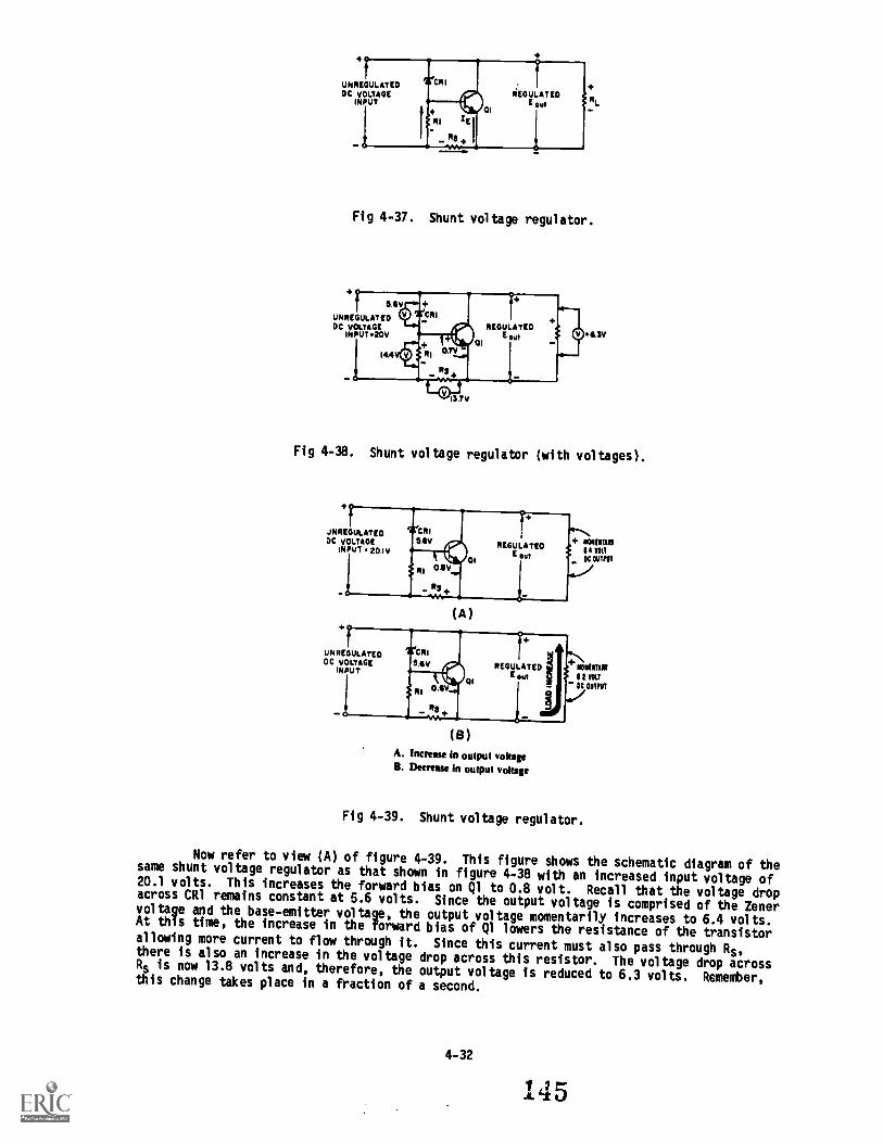
UNREGULATEDDC vOLIAGE
INPUT
Fig 4-37. Shunt voltage regulator.
5.6V
UNREGULATEDOC VOLTAGE
INPUT 20V 6.3V
Fig 4-38. Shunt voltage regulator (with voltages).
.INREGULATEDDC VOLTAGE
INPUT 20 IVIONDITAIT84 YOUDC OOTPUT
(A)
UNREGULATEDOC VOLTAGE
INPUT
( 8)A. Increase In output voltageB. Decrease In output voltage
'44:\11001111AIR
I VOLT
OMIT
.4/
Fig 4-39. Shunt voltage regulator.
Now refer to view (A) of figure 4-39. This figure shows the schematic diagram of thesame shunt voltage regulator as that shown in figure 4-38 with an increased input voltage of20.1 volts. This increases the forward bias on Q1 to 0.8 volt. Recall that the voltage dropacross CR1 remains constant at 5.6 volts. Since the output voltage is comprised of the Zenervoltage and the base-emitter voltage, the output voltage momentarily increases to 6.4 volts.At this time, the increase in the forward bias of QI lowers the resistance of the transistorallowing more current to flow through it. Since this current must also pass through Rs,there is also an increase in the voltage drop across this resistor. The voltage drop acrossRs is now 13.8 volts and, therefore, the output voltage is reduced to 6.3 volts. Remember,this change takes place in a fraction of a second.
4-32
145

Study the schematic shown in view (B). Although this schematic is identical to the
other shunt voltage schematics previously illustrated and discussed, the output voltage is
different. The load current has increased causing a momentary drop in voltage output to 6.2
volts. Recall that the circuit was designed to ensure a cons ant output voltage of 6.3
volts. Since the output voltage is less than that required, changes occur in the regulator to
restore the output to 6.3 volts. Because of the 0.1-volt drop in the output voltage, the
forward bias of Ql is now 0.6 volt. The decrease in the forward bias increases the resistance
of the transistor, thereby redUcing the current flow through Q1 by the same amount that the
load current increased. The current flow through Rs returns to its normal value and
restores the output voltage to 6.3 volts.
Current regulators. You should now know how voltage regulators work to provide
constant output voltage. In some circuits it may be necessary to regulate the current
output. The circuitry which providos a constant current output is called a constant current
re ulator or just CURRENT REGULATOR. The schematic shown in figure 4-40 is a snip-lined
sc warm for a current regulator. The variable resistor shown on the schematic is used to
illustrate the concept of current regulation. You should know from your study of voltage
regulators that a variable resistor does not respond quickly enough to compensate for the
changes. Notice that an ammeter has been Included in this circuit to indicate that the
circuit shown is that of a current regulator. When the circuit functions properly, the
current reading of the ammeter remains constant. In this case the variable resistor (Ry)
compensates for changes in the load or d.c. 1np4t voltage. Adequate current regulation
results in the loss of voltage regulation. Stud:ring the schematic shown, you Ghould recall
that any increase in load resistance causes a drop in current. To maintain a constant current
flow, the resistance of Ry must be reduced whenever the load resistance increases. This
causes the total resistance to remain constant. An increase in the input voltage must be
compensated1W-by an increase in the resistance of Ry, thereby maintaining a constant
current flow. The operation of a current regulator is similar to that of a voltage
regulator. The basic difference is that one regulates current and the other regulates voltage.
OC INPUTVOLTAGE
REGULATE0CURRENT
OUTPUT
Fig 4-40. Current regulator.
Since use of a variable resistor is not a practical way to control currentfluctuation, or variation, a transistor and a Zener diode, together with necessary resistors
are used. Recall that the Zener diode provides a constant reference voltage. The schematic
shown in figure 4-41 is that of a current regulator circuit. Except for the addition of RI,
the circuit shown in the figure is similar to that of a series voltage regulator. The
resistor is connected in series with the load and senses any current changes in the load.
Notice the voltage drop across R1 and the negative voltage polarity applied to the emitter of
Ql. The voltage polarity is a result of current flowing through R1, and this negative voltage
opposes the forward bias for Ql; however, since the regulated voltage across CR1 has an
opposite polarity, the actual bias of the transistor is the difference between the two
voltages. You should see therefore that the purpose of R2 is to function as a current-limiting resisto, for the Zener diode.
DC INPUTVOLTAGE
Fig 4-41. Current regulator.
4-33

The purpose of a current regulator is to provide a constant current regardless ofchanges in the input voltage or load current. The schematic shown in figure 4-42 is that ofcircuit designed to provide a constant current of 400 milliamperes. Voltmeters are shown inthe schematic to emphasize the voltage drops across specific components. These voltages willhelp you understand how the current regulator operates. The voltage drop across the base-emmiter junction of Q1 is 0.6 volt. This voltage is the difference between the Zener voltageand the voltage drop across Rl. The 0.6-volt forward bias of Ql permits proper operation ofthe transistor. The output voltage across RL is 6 volts as shown by the voltmeter. With aregulated current output of 400 milliamperes, the transistor resistance (Rn1) is 9 ohms.This can be proved by using Ohm's law and the values shown on the schematid. In this case,current (I) is equal to the voltage drop (E) divided by the resistance (R). Therefore, 12volts divided by 30 ohms equals 0.4 ampere, or 400 milliamperes.
2.4v ECU 911+PI
i2 VOLTS 9VDC INPUTVOLTAGE
200A400 na
eV
Fig 4-42. Current regulator (with circuit values).
Since you are familiar with the basic current regulating circuitry, let's examine indetail how the various components work to maintain the constant 400-milliamperes output.Refer to the schematic shown in figure 4-43. Remember, a decrease in load resistance causes acorresponding increase in current flow. In the example shown, the load resistance RL hasdropped from 15 ohms to 10 ohms. This results in a larger voltage drop across R1 because ofthe increased current flow. The voltage drop has increased from 2.4 volts to 2.5 volts. Ofcourse, the voltage drop across CR1 remains constant at 9 volts due to its regulatingability. Because of the increased voltage drop
across R1, the forward bias on Q1 is now 0.5volt. Since the forward bias of Q1 has decreased, the resistance of the transistor increasesfrom 9 ohms to 14 ohms. Notice that the 5-ohm increase in resistance across the transistorcorresponds to the 5-ohm decrease in the load resistance. Thus, the total resistance aroundthe outside loop of the circuit remains constant. Since the circuit is a current regulator,you know that output voltage will vary as the regulator maintains a constant current output.In the figure, the voltage output is reduced to 4 volts, which is computed by multiplyingcurrent (I) times resistance (R) (400 mA x 10 ohms 4 volts).
12 VOLTS 9VDC INPUT
Fig 4-43. Current regulator (with a decrease in RL)
VOLTAGE MULTIPLIERS
You may already know how a transformer functions to increase or decrease voltage. Youmay also have learned that a transformer secondarymay provide one or several a.c. voltageoutputs which may be greater or less than the input voltage. When voltages are stepped up,current is decreased; when voltages are stepped down, current is increased.
Another method for increasing voltages is known as voltage multiplication. VOLTAGEMULTIPLIERS are used primarily to develop high voltages Where low current is requir07-11%most common application of the high voltage outputs of voltage multipliers is the anode ofcathode-ray tubes (CRT) which are used for radar scope presentations, oscilloscopepresentations, or TV picture tubes. The d.c .. output of the voltage multiplier ranges from1000 volts to 30,000 volts. The actual voltage depends upon the size of the CRT and itsequipment application.
4-34 1 /111-3t I

Voltage nultipliers may also be used as primary power supplies where a 177-volt a.c.input is rectified to pulsating d.c. This d.c. output voltage may be increased (through useof a voltage nultiplier) to as nuch as 1000 volts d.c. This voltage is generally used as theplate or screen grid voltage for electron tubes.
If you have studied transformers, you may have learned that when voltage is steppedup, the output current decreases. This is also true of voltage multipliers. Although themeasured output voltage of a voltage multiplier may be several times greater than the inputvoltage, once a load is connected the value of the output voltage decreases. Also any smallfluctuation of load impedance causes a large fluctuation in the output voltage of themultiplier. For this reason, voltage multipliers are used only in special applications wherethe load is constant and has a high impedance or where input voltage stability is not critical.
Voltage multipliers may be classified as voltage doublers, triplers, or quadruplers.The classification depends on the ratio of the output voltage to the input voltage. Forexample, a voltage multiplier that increases the peak input voltage twice is called a voltagedoubler. Voltage nultipliers increase voltages through the use of series-aiding voltagesources. This can be compared to the connection of dry cells (batteries) in series.
The figures used in the explanation of voltage multipliers show a transformer input,even though for some applications a transformer is not necessary. The input could be directlyfrom the power source or line voltage. This, of course, does not isolate the equipment fromthe line and creates a potentially hazardous condition. Most military equipment usestransformers to minimize this hazard.
DA_Tr_vi_a C112
111:414:71;""".".......
Fig 4-44. Half-wave voltage doubler.
Figure 4-44 shows the schematic for a half-wave voltage doubler. Notice thesimilarities between this schematic and those of half-wave voltage rectifiers with which youare already familiar. In fact, the doubler shown is made up of two half-wave voltagerectifiers. Cl and CR1 make up one half-wave rectifier, and C2 and CR2 make up the other.The schematic of the first half-wave rectifier is indicated by the dark lines in view (A) offigure 4-45. The dotted lines and associated components represent the other half-waverectifier and load resistor.
Notice that Cl and CR1 work exactly like a half-wave rectifier. During the positivealternation of the input cycle (vies A), the polarity across the secondary winding of thetransformer is as shown. Note that the top of the secondary is negative. At this time CR1 isforward biased (cathode negative in respect to the anode). This forward bias causes CR1 tofunction like a closed switch and a,lows current to flow the path indicated by the arrows. Atthis time, Cl charges to the peak value of the input voltage, or 200 volts, with the polarityshown.
During the period when the input cycle is negative, as shown in view (B), the polarityacross the secondary of the transformer is reversed. Note specifically that the top of thesecondary winding is now positive. This condition now forward biases CR2 and reverse biasesCR1. A series circuit now exists consisting of Cl, CR2, C2 and the secondary of thetransformer. The current flow is indicated by the arrows. The secondary voltage of thetransformer now aids the voltage on Cl. This results in a pulsating d.c. voltage of 400
volts, as shown by the waveform. The effect of series aiding is comparable to the connectionof two 200-volt batteries in series. As shown in figure 4-46, C2 charges to the sum of thesevol tages , or 400 vol ts.
4-35 -4-1 48

_CI 4/00V cRa-ati :;:ct
1 2
(A)
rico-elv annIT+0 1.4 1."
(8)
A. Posithe elterneilonB. Negathr abernedon
Fig 4-45. Rectifier action of CR1 and CR2.
The schematic shown in figure 4-47 is an illustration of a half-wave voltage tripler.When you compare figures 4-46 and 4-47, you should see that the circuitry is identical exceptfor the additional parts, components, and circuitry shown by the dotted lines. (CR3, C3 andR2 make up the additional circuitry.) By themselves, CR3, C3, and R2 make up a half-waverectifier. Of course, if you remove the added circuitry, you will once again have a half-wavevoltage doubler.
Cl Errant
Input W--faulualent
of ----NOVItanstortner
Fig 4-46. Series-aiding sources.
Fig 4-47. Hal f-wave vol tage tri pl er.View (A) of figure 4-48 shows the schematic for the voltage tripler. Notice that CR3is forward biased and functions like a closed switch. This allows C3 to charge to a peakvoltage of 200 volts at the same time Cl is also charging to 200 volts.The other half of the input cycle is shown in view (B). C2 is charged to twice theinput voltage, or 400 volts, as a result of the voltage-doubling action of the transformer andCl. At this time, C2 and C3 are used as series-aiding devices, and the output voltageincreases to the sum of their respective voltages, or 600 volts. R1 and R2 are proportionalaccording to the voltages across C2 and C3. In this case, there is a 2 to 1 ratio.
4-36
149

(A)
wov
( )
A. Positive alternationB. Negative alternation
Fig 4-48. Voltage tripler.
Fig 4-49. Full-wave voltage doubler.
The circuit shown in figure 4-49 is that of a full-wave voltage doubler. The main
advantage of a full-wave doubler over a half-wave doubler is better voltage regulation, as a
result of reduction in the output ripple amplitude and an increase in the ripple frequency.
The circuit is, in fact, two half-wave rectifiers. These rectifiers function as series-aiding
devices except in a slightly different way. During the alternation when the secondary of the
transformer is positive at the top Cl charges to 200 volts through CR1. Then, when the
transformer secondary is negative at the top, C2 charges to 200 volts through CR2. R1 and R2
are of equal value, balancing resistors which stabilize the charges of the two capacitors.
Resistive load RL is connected across C1 and C2 so that RL receives the total charge of
both capacitors. The output voltage is +400 volts when measured at the top of RL, or point
"A" with respect to point "B." If the output is measured at the bottom of RL, it is -400
volts. Either way, the output is twice the peak value of the a.c. secondary voltage. As you
may have guessed, the possibilities for voltage multiplication are almost unlimited.
Short circuit protection. The main disadvantage of a series regulator is that the
pass trans s or Is In ser es witn the load. If a short develops in the load, a large amount
of current will flow in the regulator circuit. The pass transistor can be damaged by this
excessive current flow. You can place a fuse in the circuit, but in many cases, the
transistor will be damaged before the fuse blows. The best way to protect this circuit is to
limit the current automatically to a safe value. A series regulator with a current-limiting
circuit is shown in figure 4-50. You should recall that in order for a silicon NPN transistor
to conduct, the base must be between 0.6 volt to 0.7 volt more positive than the emitter.
Resistor R4 will develop a voltage drop of 0.6 volt when the load current reaches 600
milliamperes. This is illustrated using Ohm's law:
E 0.6 volt . .6 ampere or 600 milliamperesR 1 ohm
When load current is below 600 milliamperes, the base-to-emitter voltage on Q2 is not high
enough to allow Q2 to conduct. With Q2 cut off, the circuit acts like a series regulator.
4-37 150

Fig 4-60. Series regulator with current limiting.
*en the loed current increases above 600 milliamperes, the voltage drop across R4Increeses te more then 0.6 volt. This causes 02 to conduct throulh resistor R2, therebydecrwwmg the voltage on the base of pass transistor Ql.This action causes Q1 to conductless Therefore, the current cannot increase above 600 to 700 milliamperes.
ly increasing the value of R4, you can limit the current to almost any value Forxample, a 100-ohm resistordevelops a voltage drop of 0.6 volt at 6 milliamperes of current.You may encounter current-limiting
circuits that are more sophisticated, but the theory ofoperation is always the same. So, if you understand this circuit, the others should be noproblem.
EXERCISE:
1.
2.
3.
I.
S.
6.
7.
S.
9.
10.
11.
Answer the following questions end checkthe end of this stud). unit.
Circuits uhich meintain constant voltagevoltage or d.c. current
The purpose of a voltage regulator is tono
your responses against those listed at
or current outputs are called d.c.
provide an output voltage with little or
Ihe two basic types of voltage regulators are:
a . .111,.
b.
When a series voltage regulator is used to control output voltages, any increasein the input voltage results inin the resistance ofthe refilating device.
The shunt-type voltage regulator is connected inwith the load resistance.
In figure 4-37, the voltage drop across Rs and Ili_ determines the amount ofbase -emitterfor Ql.
In figure $-39, view (A), when there is an increase in the input voltage, theforwent bias of 01
In view (8) of figure 4-39, when the load current increases and the output voltagelamentarily drops, the resistance of Q1to compensate.
In figure 4-40, when there is an increase in the load resistance (RO, theresistance of 14to compensate for the change.
In figure 4-43 any decrease in the base-emitter forward bias across Q1 resultsinin the resistance of the transistor.
A half-weve voltage doubler is made up of how many half-wave rectifiers?
4-38 151

12. If a half-wave rectifier is added to a half-wave voltage doubler, the resulting
circuit is a voltage
13. In a full-wave voltage doubler, are the capacitors connected in series or inparallel with the output load?
Work Unit 4-3. TROUBLE-SHOOTING POWER SUPPLIES
STATE SAFETY PRECAUTIONS WHEN WORKING WITH ELECTRONIC POWER SUPPLIES.
NAME SEVERAL FAULTY COMPONENTS THAT CAN BE IDENTIFIED THROUGH VISUAL CHECKS.
SPECIFY PROBLEMS WITHIN SPECIFIC AREAS OF A POWER SUPPLY BY USING A LOGICAL
ISOLATION METHOD OF TROUBLESHOOTING.
Whenever you are working with electricity, the proper use of safety precautions is of
the utmost importance to remember. In the front of all electronic technical manuals, you will
always find a section on safety precautione. Also posted on each piece of equipment should be
a sign listing the specific precautions for that equipment. One area that is sometimes
overlooked and is a hazard is the method in which equipment is grounded. By grounding the
return side of the power transformer to th.; metal chassis, the load being supplied by the
power supply can be wired directly to the metal chassis. Thereby, the necessity of wiring
directly to the return side of the transformer is eliminated. This method saves wire and
reduces the cast of building the equipment. But, it solves one of the problems of the
manufacturer, it creates a problem for you, the technician. Before starting to work on anyelectronic or electrical equipment, ALWAYS ENSURE THAT THE EQUIPMENT AND ANY TEST EQUIPMENTYOU ARE USING IS PROPERLY GROUNDED AND THAT THE RUBBER MAT YOU ARE STANDING ON IS IN GOOD
CONDITION. As long as you follow these simple rules, you should be able to avoid the
1011517ty of becoming an electrical conductor.
TESTING
There are two widely used checks in testing electronic equipment, VISUAL and SIGNAL
TRACING. The importance of the visual check should not be underestimated biEiRe manyriEFricians find defects right away simply by looking for them. A visual check does not take
long; in fact, you should be able to see the problem in about two minutes if it is the kind of
problem that can be seen. You should learn the following procedure. You will find yourself
using it quite often as it is good not only for power supplie4 but also for any type of
electronic equipment you may be troubleshooting. (Because diode and transistor testing were
discussed earlier, it will not be discussed at this time.)
a. BEFORE YOU PLUG IN THE EQUIPMENT, LOOK FOR:
(1) Shorts. Any terminal or connection that is close to the chassis or to any other
lerrTrnal should be examined for the possibility of a short. A short in any part
of the power supply can cause considerable damage. Look for and remove any stray
drops of solder, bits of wire, nuts, or screws. It sometimes helps to shake the
chassis and listen for any tell-tale rattles. Remember to correct any problemthat may cause a short circuit; if it is not causing trouble now, it may cause
problems in the future.
(2) Discolored or leaking transformer. This is a sure sign that there is a short
somewhere. Locate it. If the equipment has a fuse, find out why the fuse did nutblow; too large a size mly have been installed, or there may be a short across the
fuse holder.
(3) Loose, broken, or corroded connections. Any connection that is not in good
condition is a trouble spot. If it is not causing trouble now, it will probably
cause problems in the future. Fix it.
(4) Damaged resistors or capacitors. A resistor that is discolored or charred has
been subjected to an overload. An electrolytic capacitor will show a whitish
deposit at the seal around the terminals. Check for a short whenever you notice a
damaged resistor or a damaged capacitor. If there is no short, the trouble may be
that the power supply has been overloaded in some way. Make a note to replace the
part after signal tracing. There is no sense in risking a new part until the
trouble has been located.
1524-39
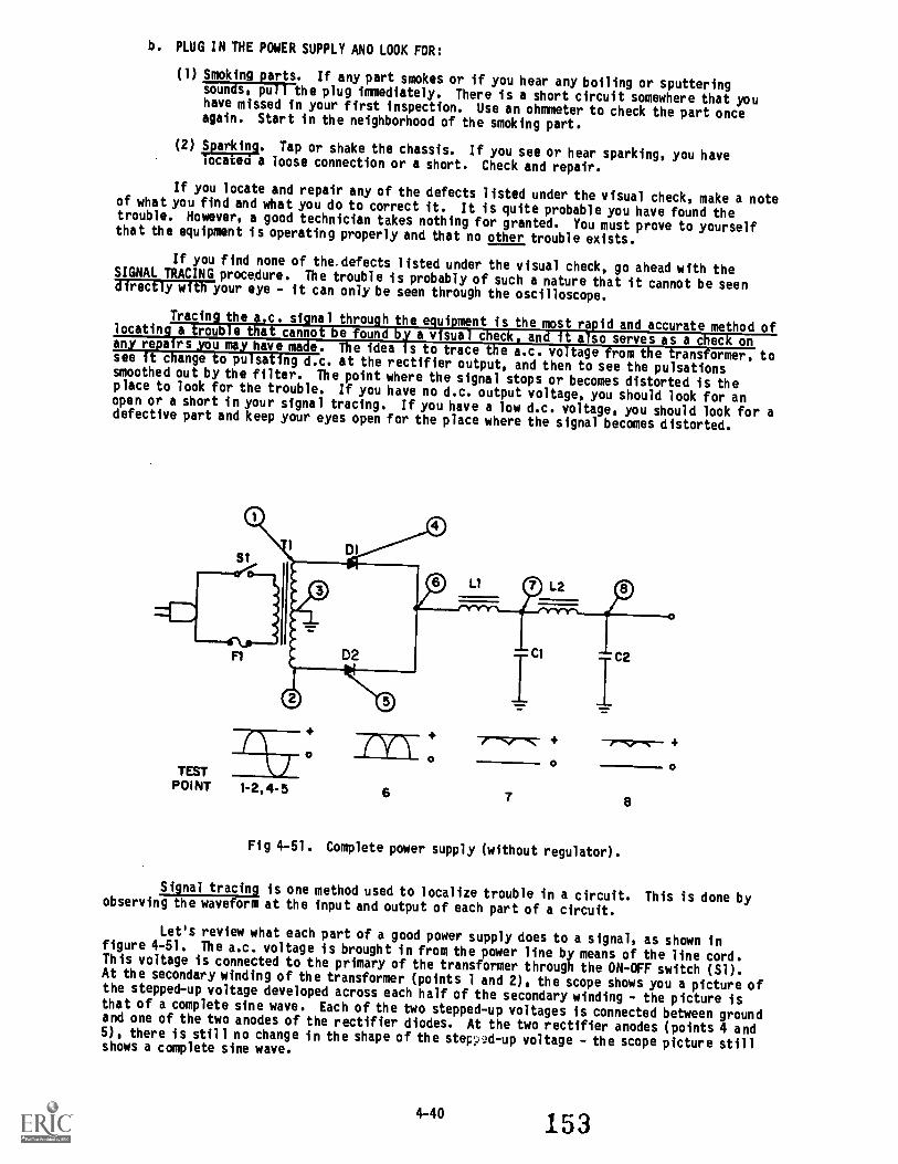
b. PLUG IN THE POWER SUPPLY AND LOOK FOR:
(1) Smoking parts. If any part smokes or if you hear any boiling or sputteringsounds, pull the plug immediately. There is a short circuit somewhere that youhave missed in your first inspection. Use an ohmmeter to check the part onceagain. Start in the neighborhood of the smoking part.
(2) Sparkin2. Tap or shake the chassis. If you see or hear sparking, you haveTocated a loose connection or a short. Check and repair.
If you locate and repair any of the defects listed under the visual check, make a noteof what you find and what you do to correct it. It is quite probable you have found thetrouble. However, a good technician takes nothing for granted. You must prove to yourselfthat the equipment is operating properly and that no other trouble exists.
If you find none of the.defects listed under the visual check, go ahead with theSIGNAL TRACING procedure. The trouble is probably of such a nature that it cannot be seendirectly with your eye - it can only be seen through the oscilloscope.
Tracing the a.c. signal through the equipment is the most rapid and accurate method oflocatingLa trouble that cannot be found by a visual check, and it also serves as a check onany repairs you may, have made. The idea is to trace the a.c. voltage from the transformer, tosee it change to pulsating d.c. at the rectifier output, and then to see the pulsationssmoothed out by the filter. The point where the signal stops or becomes distorted is theplace to look for the trouble. If you have no d.c. output voltage, you should look for anopen or a short in your signal tracing. If you have a low d.c. voltage, you should look for adefective part and keep your eyes open for the place where the signal becomes distorted.
TESTPOINT
6
0
7
Fig 4-51. Complete power supply (without regulator).
8
0
Signal tracin2 is one method used to localize trouble in a circuit. This is done byobserving the waveform at the input and output of each part of a circuit.
Let's review what each part of a good power supply does to a signal, as shown infigure 4-51. The a.c. voltage is brought in from the power line by means of the line cord.This voltage is connected to the primany of the transformer through the ON-OFF switch (51).At the secondary winding of the transformer (points 1 and 2), the scope shows you a picture ofthe stepped-up voltage developed across each half of the secondary winding - the picture isthat of a complete sine wave. Each of the two stepped-up voltages is connected between groundand one of the two anodes of the rectifier diodes. At the two rectifier anodes (points 4 and5), there is still no change in the shape of the steppA-up voltage - the scope picture stillshows a complete sine wave.
4-40 153
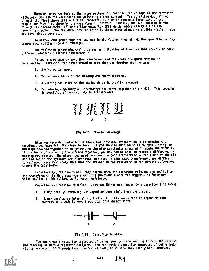
However, when you look at the scope pattern for point 6 (the voltage at the rectifier
cathodes), you see the wave shape for pulsating direct current. The pulsating d.c. is fed
through the first choke (L1) and filter capacitor (C1) which remove a large part of theripple, or "hum," as shown by the wave form for point 7. Finally, the d.c. voltage is fed
through the second choke (L2) and filter capacitor (C2) which remove nearly all of the
remaining ripple. (See the wave form for point 8, which shows almost no visible ripple.) You
now have almost pure d.c.
No matter what power supplies you use in the future, they all do the same thing - they
change a.c. voltage into d.c. voltage.
The following paragraphs will give you an indication of troubles that occur with manydifferent electronic circuit components.
As you Should know by now, the transformer and the choke are quite similar in
construction. Likewise, the basic troubles that they can develop are the same.
1. A winding can open.
2. Two or more turns of one winding can short together.
3. A winding can short to the casing which is usually grounded.
4. Two windings (primary and secondary) can short together (fig 4-52). This trouble
is possible, of course, only in transformers.
_111 3111( )11. 2. 3. 4.
Fig 4-52. Shorted windings.
When you have decided which of these four possible troubles could be causing thesymptoms, you have definite steps to take. If you surmise that there is an open winding, or
windings shorted together or to ground, an ohmmeter continuity check will locate the trouble.If the turns of a winding are shorted together, you may not be able to detect a difference in
winding resistance. Therefore, you need to connect a good transformer in the place of the old
one and see if the symptoms are eliminated; but keep in mind that transfbrmers are difficult
to replace. Make absolutely sure that the trouble is not elsewhere in the circuit before youchange the transformer.
Occasionally, the shorts will only appear when the operating voltages are applied to
the transformer. In this case you might find the trouble with the megger - an instrumentwhich applies a high voltage as it reads resistance.
Capacitor and resistor troubles. Just two things can happen to a capacitor (fig 4-53):
1. It may open up, removing the capacitor completely from the circuit.
2. It may develop an internal short circuit. This means that it begins to passcurrent as though it were a resistor or a direct short.
--1I. 2.
Fig 4-53. Capacitor troubles.
You may check a capacitor suspected of being open by disconnecting it from the circuit
and checking it with a capacitor analyzer. You can check a capacitor suspected of being leakywith an ohmmeter; if it reads less than 500 kilohms, it is more than likely bad. However,
4-41 154

capacitor troubles are difficult to find since they may appear intermittently or only underoperating voltages. Therefore, the best check for a faulty capacitor is to replace it withone known to be good. If this restores proper operation, the fault was in the capacitor.
Resistor troubles are the simplest, but like the rest, you must keep them in mind.
1. A resistor can open.
2. A resistor can increase in value.
3. A resistor can decrease in value.
1- -\t"2.
3.
Fig 4-54. Resistor troubles.
You already know how to check possible resistor troubles. Just use an ohmmeter aftermaking sure no parallel circuit is connected across the resistor you wish to measure. Whenyou know a parallel circuit is connected across the resistor or when you are in doubt,disconnect one end of the resistor before measuring it. The ohmmeter check will usually beadequate. However, never forget that occasionally intermittent troubles may develop inresistors as well as in any other electronic parts.
Although you may observe problems that have not been covered specifically in thistopic, you should have gained enough knowledge to localize and repair any problem that mayoccur.
EXERCISE: Answer the following questions and check your responses against those listed atthe end of this study unit.
1. What is the most important thing to remember when troubleshooting?
2. What is the main reason for grounding the return side of the transformer to thechassis?
3. What are two types of checks used in trouble-shooting power supplies?
a.
b.
4. What does a discolored or leaking transformer indirate?
5. A resistor that is discolored or charred has been subjected to an
. 5 154-42
6. You may check a capacitor suspected of being open by
7. You may check a capacitor suspected of being leaky with an ohmmeter. If it reads
less than , it is more than likely bad.
SUMMARY REVIEW
After completing this study unit, you have learned to identify the various componentsthat comprise a power supply and the purpose of each component. You have learned to identifythe various types of rectifier circuits and filter circuits used in a power supply. You have
learned how a.c. and d.c. current flows in a power supply. Lastly, you learned how toidentify faulty components through visual checks and problems within specific areas of a powersupply by using a logical isolation method of trouble-shooting.
Answers to Study Unit #4 Exercises
Work Unit 4-1.
1. a. Transformerb. Rectifierc. Filterd. Regulator
2. To change a.c. to pulsating d.c.3. To change pulsating d.c. to pure d.c.4. To maintain a constant voltage to the load5. The half-wave rectifier6. 15.9 volts7. It isolates the chassis from the power line.8. The fact that the full-wave rectifier uses the full output of the transformer.9. 120 hertz
10. 63.7 volts11. Peak voltage is half that of the half-wave rectifier12. The bridge rectifier can produce twice the voltage with the same size transformer
as a conventional full-wave rectifier.13. It will decrease because capacitance is inversely proportional to
Xc (Xc = 1 ).
--7--fC14. The capacitor filter15. In parallel16. At a high frequency17. A filter circuit increases the average output voltage.18. Value of capacitance and load resistance19. Good filtering20. Yes21. The cemf of the inductor22. From 1 to 20 henries23. Decrease24. Increase25. When ripple must be held at an absolute minimum26. LC capacitor-input filter27. a. cost
b. size of the inductor
Work Unit 4-2.
1. regulators2. variation3. a. Series
b. Shunt4. an increase5. in parallel6. bias7. increases8. increases9. decreases
10. an increase11. two12. tripler
13. in parallel4-43
I 5 6

Work Unit 4-3.
1. Safety precautions2. To eliminate shock hazard3. a. Visual
b. Signal tracing4. That a short exists somewhere5. Overload6. disconnecting it form the circuit and checking it with a capacitor analyzer7. 500 kilohms
1 5 74-44

SOLID STATE DEVICES
REVIEW LESSON
INSTRUCTIONS: This review lesson is designed to aid you in preparing for your final exam.You should try to complete this lesson without the aid of reference materials, but if you donot know an answer, look it up and remember what it is. The enclosed answer sheet must befilled out according to the instructions on its reverse side and mailed to MCI using the
envelope provided. The questions you miss will be listed with references on a feedback sheet(MCI-R69) which,will be mailed to your commanding officer with your final exam. You should
study the reference material for the questions you missed before taking the final exam.
A. Multiple Choice: Select the ONE answer that BEST completes the statement or answers the
question. After the corresponding number on the answer sheet, blacken the appropriate
circle.
Value: 1 point each
1. Identify a solid state device?
a. A device that operates by magnetic motionb. A device that is classified as an insulatorc. An electronic device which operates by virtue of the movement of electrons within
a solid piece of semiconductor materiald. An electronic device which operates by the movement of protons
2. Identify the term negative temperature coefficient.
a. It is the decrease in a semiconductor's resistance as temperature rises.
b. It is the difference between negative and positive.
c. It is pure resistance.
d. It is the increase in a conductor's resistance as temperatures rise.
3. Space systems and computers are two of the three largest users of semiconductor
devices. Identify the other large user.
a. Cars c. Home computers
b. Data processing equipment d. High schools
4. Identify one requirement of an electron tube which does not exist for semiconductors.
a.
b.
C.
d.
The electron tube requiresThe electron tube requiresdevice does not.
The electron tube requiresThe semiconductor requiresdoes not.
a transistor to function.filament or heater voltage whereas the semiconductor
a diode.filament or heater voltage; whereas, the electron tube
5. What makes the electron tube less efficient than the semiconductor?
a. No power input is spent by the semiconductor for conduction
b. The tube is smaller that the semiconductor.
c. No power input is spent by the electron tube for conduction.
d. Lower resistance exists in the electron tube.
6. Matter is defined as
a. anything that can not be seen.
b. anything that you can touch.c. all liquids.d. anything that occupies space and has weight.
7. Matter is made up of what three different states?
a. Gas, liquid, and solid c. Temperature, humidity, and solid
b. Air, water, and earth d. Temperature, moisture, and solid
R-1

8. The outer shell of an atom is called the
a. valence shell. c. inner shell.b. outer shell. d. forbidden shell.
9. What determines, in terms of energy bands, whether a substance is a good insulator,semiconductor, or conductor?
a. The width of the valence shell c. The type of materialb. The width of the forbidden band d. The amount of voltage
10. What term describes the sharing of valence electrons between two or more atoms?
a. Valence bonding c. Covalent bondingb. Active bonding d. Inactive bonding
11. Identify the two types of current flow in a semiconductor.
a. Electron and hole flow C. Shell and valence flowb. Electron and shell flow d. Hole and valence flow
12. What is the name given to a doped germanium crystal with an excess of free holes?
a. N-type crystal c. Active crystalb. Low crystal d. P-type crystal
13. Identify the purpose of a PN ;unction diode.
a. To convert alternating current into direct currentb. To activate direct currentc. To convert direct current into pulsating direct currentd. To convert pulsating direct current into voltage
14. Identify the direction of electron flow in reference to the schematic symbol for adiode.
a. Toward the arrow c. With the arrowb. Away from the arrow d. Both away and with the arrows
15. In order to reverse bias in a PN junction, what terminal of a battery is connected tothe P material?
a. Negative and positive terminals c. Positive terminalb. Negative d. Neither terminal
16. What type of bias opposes the PN junction barrier?
a. Reverseb. Barrier
17. What is a load?
c. Opposited. Forward
a. Any device that draws current from a power sourceb. A device that produces voltagec. A generatord. A magnet
18. Identify the output of a half-wave rectifier.
a. A pulsating a.c. voltageb. A constant d.c. voltagec. A pulsating d.c. voltaged. A pulsating a.c. and a constant a.c. voltage
19. Identify the type of bias that makes a diode act as a closed switch.
a. Reverse bias c. Forward biasb. Neutral bias d. Negative bias
R-2 159

20. What type of rectifier is constructed by sandwiching a section of semiconductormaterial between two metal plates?
a. Metallic rectifier c. Sandwiching rectifierb. Plate rectifier d. Dual rectifier
21. What is used to show how diode parameters vary over a full operating range?
a. The diode markings c. A routing sheetb. A characteristic curve d. A scale
22. What is meant by diode rating?
a. The limiting values of operating conditions outside which operations could causediode damage
b. The number that can be used in a circuitc. The purpose for the deviced. Diodes do not have ratings.
23. What does the letter "N" indicate in the semiconductor identification system?
a. A semiconductorb. Voltage potentialc. Current potentiald. It corresponds to the resistance of the device.
24. What type of diode has orange, blue, and gray bands?
a. 4N268b. 2N176
25. What is the greatest threat to a diode?
a. Currentb. Voltage
c. 1N492d. 1N368
c. Heatd. Resistance
26. When checking a diode with an ohmmeter, what is indicated by two high resistantmeasurements?
a. That the diode is open or has a high forward resistanceb. That the diode is operating properlyc. That the diode is closed or has a high reverse resistanced. That the reverse bias is too hot
27. What is the name given to the semiconductor device that has three or more elements?
a. Diode c. Transistorb. Rectifier d. Emitter
28. Identify the electronic function that made the transistor famous.
a. Amplification c. The amount of heat producedb. Voltage production d. Its appearance in the circuit
29. What was the name of the very first transistor?
a. H-contact c. TRWb. Hertz d. Point-contact
30. What is one of the most important functions of any transistor manufacturing process?
a. The numbers of transistors producedb. Proper identification of the devicec. Quality controld. Doping levels
31. To properly bias an NPm transistor, what polarity voltage is applied to the collector?
a. Negative c. Both negative and positiveb. Positive d. High polarity voltage

32. What percentage of current in an NPN transistor reaches the collector?
a. 98 percent c. 90 percentb. 95 percent d. 75 percent
33. What is the relationship to the base voltage of a properly bias NPN transistor inregards to the polarity voltage applied to the collector?
a. Equal c. More positivec. Less positive d. More negative
34. What is the relationship between the polarity of the voltage applied to the PNPtransistor and that applied to the NPN transistor?
a. The polarity of voltage applied to the PNP transistor is opposite of that appliedto the NPN transistor.
b. There is no permanent relationship.c. They both use the equal polarity voltage.d. The polarity of voltage applied to the PNP transistor is the same as that applied
to the NPN transistor.
35. Identify the two current loops in a transistor.
a. Emitter and polarity loop currentsb. Base and emitter loop currentsc. Base current and collector current loopd. Forward and reverse loop currents
36. Identify the letter designation for base current.
a. CB
b. BC
c. IC
d. Ig
37. What is the name of the device that provides an increase in current, voltage, orpower of a signal without appreciably altering the original signal?
a. Rectifier c. Amplifierb. Divider d. Emitter
38. Besides eliminating the emitter-base battery and compensating for slight variationsin transistor characteristics, what other advantage can different biasing methodsoffer?
a. Changes in transistor conduction due to polarityb. Changes in transistor conduction due to temperature variationsc. There are no other advantagesd. A potential balancing of the transistor
39. Identify the primary difference between the NPN and PNP amplifiers.
a. The number used in the amplifier c. The polarity of the source voltageb. The name of the amplifier d. The amount of current required
40. Which of the following biasing methods is the most unstable?
a. Base current bias or fixed bias c. Emitter current biasb. Collector current bias d. Element bias
41. Identify the most widely used combination-bias system.
a. The voltage-divider type c. High and low typeb. Zener diode type d. Point-contact type
42. What amplifier class of operation allows collector current to flow during thecomplete cycle of the input?
a. Class Bb. Class A
c. Class Ed. Class F
R-4 1G1

43. The two primary items that determine the class of operation of an amplifier are theamount of bias and the
a. amplitude of the input signal.b. P-type material.c. N-type material.d amplitude of the output signal.
44. Which transistor configuration provides a phase reversal between the input and outputsignals?
a. Common baseb. Common collector
45. Which transistor configuration has a
a. Gammab. Beta
c. Common emitterd. Common rectifier
current gain of less than 1?
c. Charlied. Alpha
46. The current gain in a common-base circuit is called
a. emitter current (IE). c. collector current (Ic).b. base current (43). d. source current (Is)
47. What is the formula used to compute Gamma?
a. gamma IE x IB c. gamma . IE divided by Icb. gamma m IE plus IB d. gamma m IE divided by IB
48. The information normally included in the general description section ofspecification sheet for a transistor is the
a. length, width, and height.b. kind of transistor, the trznsistor's common applications, and mechanical data.c. total to be used, the type, and mechanical data.d. type installation used, application, and current rating.
49. What does the number 112" prior to the letter "N" indicate in the JAN marking scheme?
a. The number required to operate properlyb. The number of heaters in the devicec. The number of junctions in the device which in this case indicates a transistord. That the current reading must be divided by 2 to obtain the voltage reading
a
50. Identify the greatest danger to a transistor.
a. Heat c. Currentb. Cold d. Voltage
51. Identify the method for checking a transistor which is cumbersome when more than onetransistor is bad in a circuit?
a. Forward methodb. Avalence method
52. Identify the safety precaution which
a. Add heat to aid the operation.b. The circuit must be energized.
c. Reverse methodd. Substitution method
must be taken before replacing a transistor.
c. Keep the circuit doping down.d. The power must be removed from the circuit.
53. How is the collector lead identified on an oval-shaped transistor?
a. By the wide space between the collector lead and the other two leads (emitter andbase)
b. By the color markings on the leadc. The collector lead is shorter than the other two leads.d. The collector lead is always on the left.

54. Identify the two most important parameters used for testing a transistor.
a. Current and resistanceb. Gain and leakage
55. Integrated circuits are defined as
a. two lit added by conductors.b. circuit4 packaged as a single circuitc. a master circuit aided by two minor circuits.d. two circuits separated by an insulator.
c. Gain and resistanced. Voltage and gain
56. In a reverse-biased PN junction, which current carriers cause leakage current?
a. The majority carriers c. The reverse carriersb. The forward carriers d. The minority carriers
57. What is the doping level of an avalanche effect diode when compared to the dopinglevel of a Zener effect diode?
a. The doping level of an avalence effect diode is lower.b. The doping levels are equal.c. The doping level of an avalence effect diode is higher.d. The doping level is twice that of the Zener effect diode.
58. Why is electron flow with the arrow in the symbol of a Zener diode instead of againstthe arrow as it is in a normal diode?
a. Because it iblicates a combination bias methodb. Because Zener diodes are operated in the reverse-bias modec. Because that is the way all diodes are manufacturedd. Because Zener diodes are operated in the forward bias mode
59. Identify the main difference in construction between normal PN junction diodes andtunnel diodes.
a. The amount of voltage c. The number of inner shellsb. The number of outer shells d. The amount of doping
60. What resistance property is found in tunnel diodes but not in normal diodes?
a. Positive resistance c. Positive currentb. Negative resistance d. Negative current
61. In the tunnel diode, the tunneling current is at what level when the forbidden gap ofthe N-type material is at the same energy level as the empty states of the P-typematerial?
a. Maximumb. Minimum
c. The same leveld. Doping level
62. The varactor displays what useful electrical property?
a. Variable impedance c. Variable capacitanceb. Limiting d. Active
63. When the reverse bias on a varactor is increased, what, if anything, happens to theeffective capacitance?
a. The capacitance decreases c. Nothing happensb. The capacitance increases d. The capacitance will be balanced
64. The SCR is primarily used for what function?
a. To switching power on or off c. To switch power offb. To switch power on d. As a filter
65. When an SCR is forward biased, what is needed to cause it to conduct?
a. The zener signal c. The cathode signalb. Collector current d. The gate signal
66. What is the only way to cause an SCR to ..top conducting?
a. By reducing reverse biasb. By increasing the doping levelc. By decreasing the doping leveld. The forward bias must be reduced below the minimum conduction level
67. The triac is similar in operation to what device?
a. SCRb. Transistor
c. Dioded. LED
68. When used for a.c. current control, during which alternation of the a.c. cycle doesthe triac control current flow?
a. During both alternations c. During the negative alternationb. During the positive alternation d. During neither alternation
69. The functions of a triac can be duplicated y connecting two actual
a. diodes. c. SCRs.b. transistors. d. Zener diodes.
70. The LED, photocell, and solar cell are three of the five types of optoelectronicdevices. Identify the remaining two.
a. Transistor and zener diodeb. Photodiode and the photo.ransistorc. Thyratron and SCRd. SCR and triac
71. Identify the type of bias that is required to cause an LED tc produce light.
a. RPverse bias c. Neutral biasb. Both reverse and forward bias d. Forward bias
72. When compared to incandescent lamps, what is the power requirement of an LED?
a. Very lowb. Very high
c. Equald. Zero
73. In a common anode, seven-segment LED display, an individual LED will light if anegative voltage is applied to what element?
a. The cathode c. The baseb. The anode d. The point emitter
74. What is the resistance level of a photodiode in total darkness?
a. Equal
b. Zeroc. Very lowd. Very high
75. What is a typical light-to-darkness resistance ratio for a photocell?
a. 2:1
b. 1:500c. 1:1000
d. 2:1000
76. Identify the semiconductor device that produces electrical energy when exposed tolight?
a. Photovoltaic cellb. Transistor
c. PhotoLEDd. Diode
R-7 1 64

77. The unijenctIon transistor (UJT) has how many PN Junctions?
a. Threeb. Too
c. Oned. Zero
78. The area between base 1 and base 2 In a unijunction transistor acts as what type ofcommon circuit component?
a. Variable resistor c. Triacb. SCR d. Voltage divider
79. Identify the news of the sequential rise in voltage between the two bases of theunijunction transistor.
a. Gage bias C. A gate gradientb. Voltage bias d. A voltage gradient
80. Identify the normal current path for a unijunction transistor.
a. From base 2 to the emitter c. From base 1 to the emitterb. From base 2 to the collector d. From base 1 to the collector
$I. Identify the one advantage of the field effect transistor (FET) %ten compared to thebipolar transistor.
a. Nigh input capacitance c. Nigh Input Impedanceb. Low input impedance d. Low input capacitance
82. Identify two types of Junction field effect transistor?
a. Forwerd and reverse c. Voltage and currentb. N-channel and P-channel d. Resistance and current
83. Identify the key to the field effect transistor (FEY) operation.
o. Effective cross-sectional area of the channelb. The amount of current flowC. A positive gate voltaged. Reverse biasing
84. Whop compared to the Junction field effect transistor (JFET), what is the inputimpedance of the metal oxide semiconductor field effect transistor (NOSFET)?
a. The NOSFET has a lower input impedanceb. There is no difference.c. It is balanced.d. The NOSFET has a higher input impedance.
$S. What are the four elements of the NOSFET?
a. Gate, heater, filament, and drainb. Gate, source, drain, and substiateC. Source, gate, heater, and file...atd. Drain, resistance, source, and substrate
U. TheleGMET is normally constrected so that it can operate in one of two basic modes;the depletion mode or the
a. negative mode. C. enhancement mode.b. filter mode. d. regulator mode.
87. Identify the foer sections of a power supply.
a. Rectifier, diode, gate, and filterb. Transformer, rectifier, filter, regulatorc. Filter, regulator, switch, and gated. Regelator, filter, switch, and source
it-11 1G5

88. Identify the section of
a. Rectifier sectionb. Gate section
the power supply that changes a.c. to pulsating
c. Filter sectiond. Diode section
d.C
89. Identify the section of the power supply that changes pulsating d.c. to pure d.c.
a. Gate c. Rectifierb. Transformer d. Filter section
90. What is the purpose of the regulator section of
a.
b.
c.
d.
To maintain a constant voltage to the loddTo decrease the voltage to the loadTo separate the output of the sourceTo maintain a constant sinewave
91. In addition to stepping up or stepping dopurpose does the transformer serve?
a. To transform a.c. to d.c. c.
b. It changes current direction d.
92. What is the major factor that led to the
the power supply?
wn the input line voltage, what additional
a. The fact that the full-wave rectifierb. It keeps the LEDS operating properly.c. It uses fewer SCRs.d. The fact that it uses the full ouput
93. What is the average voltage (Eavg) outputof 100 volts peak?
It isolates the chassis from the power lineNone
development of the full-wave rectifier?
uses the full output of the transformer
of the transformer
of a full-wave rectifier with an output
a. 53.7 volts c. 63.7 voltsb. 60.7 volts d. 67.3 volts
94. What is the main disadvantage of a conventional full-wave rectifier?
a.
b.
c.
d.
Peak current is twice that of the half-wave rectifierPeak voltage is twice that of the half-wave rectifierPeak current is half that of the half-wave rectifierPeak voltage is half that of the half-wave rectifier
95. What main advantage does a bridge rectifier have over a conventionalrectifier?
a.
b.
c.
d.
full-wave
Current limiting abilityIt is better insulated for your protectionThe transformer gets hot.
The bridge rectifier can produce twice the voltage with the same size transformer.
96. Identify the most basic type of filter.
a. The capacitor filterb. The resistance filter
c. Thed. The
inductance filtervoltage filter
97. The rate of discharge of a capacitor in a filter circuit is determined by the
a.
b.
c.
d.
value of capacitance and load resistance.size of the circuit.gate signal.circuit design.
98. Identify what prevents the rapid charging of the capacitorfilter?
in an LC choke-input
a. The ripple frequency c. Pulsating voltageb. Change time d. The cemf of the inductor

99. If the impedance of the choke is increased, what will happen to the ripple frequency?
a. It will decrease c. It will remain the same.b. It will increase d. It will become unequal.
100. When is a second RC filter stage used?
a. When the ripple must be held at an absolute maximumb. When the pulsating voltage is first appliedc. When the ripple must be held at an absolute minimumd. When the capacitor is connected across the output
101. Circuits which maintain constant voltage or current outputs are called d.c. voltageor d.c. current
a. filters. c. regulators.b. rectifiers. d. transformers.
102. The purpose of a voltage regulator is to provide an output voltage with little or no
a. resistance. c. impedance.b. current. d. variation.
103. Identify the two basic types of voltage regulators.
a. Half-wave and full-wave c. Parallel and binderb. Series and shunt d. Series and binder
104. When a series voltage regulator is used to control output voltages, any increase inthe input voltages results in in the resistance of theregulating device.
a. a decrease c. an increaseb. a ripple effect d. filtering action
105. Identify how a shunt-type voltage regulator is connected with the load resistance.
a. In parallel c. In series-parallelb. In series d. Positive in respect to the cathode
UNREGULATEDDC VOLTAGE
INPUT
1 1
REGULATEDE
106. In the figure above, the voltage drop across Rs and R1 determines the amount ofbase-emitter for Ql.
a. bias c. filteringb. resistance d. ripple frequency
R-10
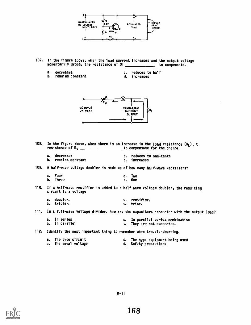
UNREGULATEDDC VOLTAGE
INPUT 201VREGUL AT ED
t oul
+ NONDTAIG14 VOLTDC OUTPUT
107. In the figure above, when the load current increases and the output voltagemomentarily drops, the resistance of 01 to compensate.
a. decreases c. reduces to halfb. remains constant d. increases
DC INPUT REGULATEDVOLTAGE CURRENT
OUTPUT
11.
108. In the figure above, when there is an increase in the load resistance (110, tresistance of RI/ to compensate for the change.
a. decreases c. reduces to one-tenthb. remains constant d. increases
109. A half-wave voltage doubler is made up of how many half-wave rectifiers?
a. Four c. Twob. Three d. One
110. If a half-wave rectifier is added to a half-wave voltage doubler, the resultingcircuit is a voltage
a. doubler. c. rectifier.b. tripler. d. triac.
111. In a full-wave voltage divider, how are the capacitors connected with the output load?
a. In series c. In parallel-series combinationb. In parallel d. They are not connected.
112. Identify the most important thing to remember when trouble-shooting,
a. The type circuit c. The type equipment being usedb. The total voltage d. Safety precautions
R-11
168

113. What is the main reason for groundlig the return side of the transformer to thechassis?
a. To prevent damage to the transformerb. For the proper operation of the equipmentc. Because it is a Marine Corps requirementd. To eliminate electrical shock
114. What are two types of checks used in trouble-shooting power supplies?
a. Mechanical and chemical c. Visual and signal tracingb. Physical and visual d. Rogets and Thesaurus tracing
115. Identify what is indicated by a discolored or leaking transformer.
a. That a short exists somewhere c. Significant changes in designb. An open circuit d. Solid state components
116. A discolored or charred resistor has been subjected to a(n)
a. overload. c. inexpericened technician.b. high resistance. d. filter.
117. To check a capacitor suspected of being open, first disconnect it from the circuitand check it with a(n)
a. capacitor analyzer.b. voltmeter.
c. ohmmeter.d. SCR.
118. You may check a capacitor suspected of being leaky with an ohmmeter. If it readsless than , it is more than likely bad.
a. 300 kilohms c. 750 kilohmsb. 500 kilohms d. 1000 kilohms
Total Points: 118
169*U.S. GOVERNMENT PRINTING OFFIGEs1986-491-630140037
R-12

STUDENT COURSE CONTENT ASSISTANCE REQUEST
COURSE NUMBER COURSE TITLE DATE:
NAME RANK MOS
SOCIAL SECURITY NUMBER DATE:
COMPLETE MILITARY ADDRESS:INCLUDE RUC)
UNIT PNONE NUMBER masa FILL IN AMPS ON MUSE INDIO
1. Use this form for any questions you may have about this course. Write out your question andrefer to the study unit, work unit, or study question which you are having problems with. Com-plete the self-addressed block on the reverse side. Before mailing, fold the form and staple it sothat MCI's address is showing. Additional sheets may be attached to this side of the form. Yourquestion will be answered promptly by a Marine NCO.
MY QUESTION IS: OUR ANSWER IS:
1 7 0
SSTD-1

DEPARTMENT OF THE NAVYUNITED STATES MARINE CORPSMARINE CORPS INSTITUTEARLINGTON, VA 222224001
OPPICIAL SUSINISSMALTY FOR PRIVATI UK SMIO
MAME I SANK
MILITARY ACCRISS
',BUSINESS REPLY MAILCLASS MAW ROAM WASH., D.C.
POSTASI WILL II PAID SY U.S. NAME COMPS
UNITED STATES MARINE CORPSMARINE CORPS INSTITUTEARLINGTON, VA 22222.0001
NO POSTAGENECESSARYIF MAILED
IN THEUNITED STATES
IIMMIMMIIMMIS
ISM1111iMllOfill11MIMMEMMIMIMI=1M11111=MIMEMPIMMilIMIMIMM111
1 1

STUDENT REQUEST/INQUIRYMCI - R11
DATE SENT:DATE RECIEVED AT MCI:
COURSE NUMBER COURSE TITLE
COMPLETE ALL PORTIONS OF SECTION 1
Section 1. Student Identification
Rani%
SsN
s as name
REPOITING UNIT CODE (RUC)
n
nr el:Jur
n4 n n : rrin or ype name, ranand address clearly. Include ZIP CODE.Only Class III Reservists use civilianaddress
Section 2. CHECK THE APPROPRIATE BOX AND FILL IN THE APPROPRIATE SPACES.
FOR REGULAR AND CLASS II RESERVE MARINES THIS FORM MUST OE SIGNED BY THE COMMANDINGOFFICER OR HIS REPRESENTATIVE, i.e. TRAINING NCO.
1. EXTENSION - Please grant an extension FOR MCI uac. udLY(will not be granted if already on extension.) 1. D
2. NOTICE OF COURSE COMPLETION - Final Exam Sent 2. On SMF K LOn . (New exam will be sentiMe:Inot receives at MCI.) 3. C
3. REENROLLMENT - Student has course materials 4. L(See para. 4003 of Vol. I of MCI Catalogfor information on reenrollment.)
4. OVERDUE FINAL EXAM - Last (Review) lesson 6. Psent on . Please send exam.
7. E5. Please send new ANSWER SHEETS.
8.6. ylease send miscIng course materials (Not
included in course package.)Lessons Manual Other
7. CHANGE - Rank NameSocial Security NumberRUC
8. (explain)
Note: 'This lorm will not be7E1-lined by MCI. If requestis valid, transaction will SIGNATURE-TITLE OR RANg7show on next UAR or or (MUST BE CO OR REPRESENTATIVE)MCI-R1_ form.
DATE COMPLETED
ORIGINATOR CODE
STUDENT: Detach and retain this portion.
DATA REQUIRED BY THE PRIVACY ACT OF 1974(5 U.S.C. 522A)
1. AUTHORITY: Title 5, USC, Sec. 301. Use of your Social Security Number is authorizedby Executive Order 9397 of 22 Nov 43.
2. fkINCIPAL PURPOSE: The Student Course Content Assistance Request is used to transmitinformation concerning student participation in MCI courses.
3. ROUTINE USE: This information is used by MCI personnel to research studentinquires. In some cases information contained therein is used to update correspondencecourse and individual student records maintained by the Marine Corps Institute.
4. MANDATORY OR VOLUNTARY DISCLOSURE AND EFFECT ON INDIVIDUAL NOT PROVIDING INFORMATION:Disclosure is voluntary. Failure to provide information may result in the provision ofincomplete service to your inquiry. Failure to provide your Social Security Number willdelay the processing of your assistance request.
172

BUSINESS REPLY MAILMOT MAN AMR NO. 113111 INMINNITON 0 C
WAS, VAL II PAD IN 1111 NAOS COW
UNITED STATES MARINE CORPSMARINE CORPS INSTITUTEARLINGTON, VA 22222.0001
NO POOM011WOHIGhltvIF WINOIN Id
WO STAMM
=MEM=
111111111111111111111111111111111111111111116111111111111111111111111111111111
DETACH BEFCHE MAILING
1 7 3