dlpc350 programmer s guide (rev. e) - keynote photonics · 2.2.2 enter program mode ... csc matrix...
TRANSCRIPT

DLPC350 Programmer’s Guide
User's Guide
Literature Number: DLPU010EMay 2013–Revised February 2015

Contents
Preface ........................................................................................................................................ 51 Interface Protocol................................................................................................................. 7
1.1 I2C Interface .................................................................................................................. 71.1.1 I2C Transaction Structure .......................................................................................... 71.1.2 I2C Read Transaction Sequence.................................................................................. 81.1.3 I2C Write Transaction Sequence.................................................................................. 8
1.2 USB Interface ................................................................................................................ 91.2.1 USB Transaction Sequence ....................................................................................... 91.2.2 USB Read Transaction Sequence................................................................................ 91.2.3 USB Write Transaction Sequence .............................................................................. 10
2 DLPC350 Control Commands .............................................................................................. 122.1 DLPC350 Status Commands ............................................................................................. 12
2.1.1 Hardware Status................................................................................................... 122.1.2 System Status ..................................................................................................... 132.1.3 Main Status ........................................................................................................ 132.1.4 Retrieve Firmware Version....................................................................................... 142.1.5 Input Video Signal Detection Status ............................................................................ 14
2.2 DLPC350 Programming Commands .................................................................................... 152.2.1 Read Status ........................................................................................................ 152.2.2 Enter Program Mode.............................................................................................. 162.2.3 Read Control ....................................................................................................... 162.2.4 Start Address ...................................................................................................... 172.2.5 Erase Sector ....................................................................................................... 172.2.6 Download Data Size .............................................................................................. 172.2.7 Download Data .................................................................................................... 182.2.8 Calculate Checksum .............................................................................................. 18
2.3 Chipset Control Commands............................................................................................... 182.3.1 Chipset Configuration and Control Commands ............................................................... 182.3.2 Interface Configuration and Control............................................................................. 212.3.3 FPD-Link Interface Configuration and Control................................................................. 212.3.4 Input Source Control .............................................................................................. 232.3.5 Image Flip .......................................................................................................... 272.3.6 Image Processing Control........................................................................................ 282.3.7 LED Driver Control ................................................................................................ 292.3.8 GPIO Control....................................................................................................... 322.3.9 Pulse Width Modulated (PWM) Control ........................................................................ 332.3.10 PWM Enable ...................................................................................................... 342.3.11 PWM Capture Configuration .................................................................................... 342.3.12 PWM Capture Read ............................................................................................. 35
2.4 Display Sequences......................................................................................................... 352.4.1 Display Mode Selection Command ............................................................................. 382.4.2 Video Mode Commands.......................................................................................... 392.4.3 Pattern Display Commands ...................................................................................... 40
3 Power-Up and Power-Down and Initialization Considerations .................................................. 583.1 Power Up .................................................................................................................... 58
2 Contents DLPU010E–May 2013–Revised February 2015Submit Documentation Feedback
Copyright © 2013–2015, Texas Instruments Incorporated

www.ti.com
3.2 Power Down ................................................................................................................ 583.3 Power-Up Auto-Initialization .............................................................................................. 58
4 Pattern Display Mode Examples ........................................................................................... 604.1 Pattern Display Mode Example........................................................................................... 604.2 Trigger Mode 0 Example .................................................................................................. 624.3 Variable Exposure Pattern Sequence Example ........................................................................ 634.4 Variable Exposure Video Streaming Pattern Sequence Example ................................................... 64
A Register Quick Reference .................................................................................................... 66A.1 I2C Register Quick Reference ............................................................................................ 66A.2 Command Guide ........................................................................................................... 68
Revision E History....................................................................................................................... 71Revision D History....................................................................................................................... 71Revision C History....................................................................................................................... 71Revision B History....................................................................................................................... 72Revision A History....................................................................................................................... 72
3DLPU010E–May 2013–Revised February 2015 ContentsSubmit Documentation Feedback
Copyright © 2013–2015, Texas Instruments Incorporated

www.ti.com
List of Figures1-1. I2C Read Register Sequence .............................................................................................. 81-2. I2C Write Register Sequence ............................................................................................... 91-3. USB HID Protocol............................................................................................................ 92-1. Image Long-Axis Flip Example ........................................................................................... 282-2. Image Short-Axis Flip Example........................................................................................... 282-3. CSC Matrix .................................................................................................................. 292-4. DLPC350 Functional Block Diagram .................................................................................... 362-5. Bit-Planes of a 24-Bit RGB Image ....................................................................................... 372-6. Bit Partition in a Frame for an 8-Bit Monochrome Image ............................................................. 372-7. DLP4500 Frame Buffer .................................................................................................... 382-8. Frame Delay Between RGB Input and Video Output.................................................................. 382-9. Trigger Mode 0 Timing Diagram Example .............................................................................. 422-10. Trigger Mode 1 Timing Diagram Example .............................................................................. 422-11. Trigger Mode 2 Timing Diagram Example .............................................................................. 432-12. Flowchart Example for Programming 1280 Variable Exposures..................................................... 56
DLP is a registered trademark of Texas Instruments.
4 List of Figures DLPU010E–May 2013–Revised February 2015Submit Documentation Feedback
Copyright © 2013–2015, Texas Instruments Incorporated

PrefaceDLPU010E–May 2013–Revised February 2015
Read This First
About This ManualThis document specifies the command and control interface to the 0.45 WXGA chipset. It also defines allapplicable commands, default settings, and control register bit definitions to communicate with the 0.45WXGA chipset.
Related Documents from Texas Instruments• DLP® 0.45 WXGA Chipset: DLP 0.45 WXGA Chipset Data Manual, DLPU009• DLPC350 Data Sheet: DLP Digital Controller for DLP4500 DMD, DLPS029• DLP4500 Data Sheet: DLP 0.45 WXGA DMD, DLPS028
If You Need AssistanceSee the DLP and MEMS TI E2E Community support forums.
DLP is a registered trademark of Texas Instruments.
5DLPU010E–May 2013–Revised February 2015 Read This FirstSubmit Documentation Feedback
Copyright © 2013–2015, Texas Instruments Incorporated

If You Need Assistance www.ti.com
6 Read This First DLPU010E–May 2013–Revised February 2015Submit Documentation Feedback
Copyright © 2013–2015, Texas Instruments Incorporated

Chapter 1DLPU010E–May 2013–Revised February 2015
Interface Protocol
This chapter describes the interface protocol between the DLPC350 and a host processor. The DLPC350supports two host interface protocols: I2C and USB 1.1 slave interfaces.
1.1 I2C InterfaceThe DLPC350 controller uses the I2C protocol to exchange commands and data with a host processor.The I2C protocol is a two-wire serial data bus that conforms to the NXP I2C specification, up to 100 kHz.One wire, SCL, serves as a serial clock, while the second wire, SDA, serves as serial data. Severaldifferent devices can be connected together in an I2C bus. Each device is software addressable by aunique address. Communication between devices occurs in a simple master-to-slave relationship.
1.1.1 I2C Transaction StructureAll I2C transactions are composed of a number of bytes, combined in the following order:
START Condition, Slave Address Byte + R/W Bit, Sub-Address Byte, N-Data Bytes, STOP Conditionwhere N in "N-Data Bytes" varies based on the sub-address.
1.1.1.1 I2C START ConditionAll I2C transactions begin with a START condition. A START condition is defined by a high-to-lowtransition on the SDA line, while the SCL line is high.
1.1.1.2 DLPC350 Slave AddressThe DLPC350 offers two different slave addresses. The I2C_ADDR_SEL pin of the DLPC350 provides theability to select an alternate set of 7-bit I2C slave addresses. If the I2C_ADDR_SEL pin is low, then theDLPC350 slave address is 0x1A. If the I2C_ADDR_SEL pin is high, then the DLPC350 slave address is0x1D. Because the first 8-bit I2C packet includes the 7-bit slave address followed by a read (high) or write(low) bit, a read command to the DLPC350 concatenates the slave address with a 1. A write command tothe DLPC350 concatenates the slave address with a 0. Thus, when I2C_ADDR_SEL is low, the DLPC350first byte packet of an I2C command is 0x34 for write and 0x35 for read. When I2C_ADDR_SEL is high,the DLPC350 first byte packet of an I2C command is 0x3A for write and 0x3B for read.
1.1.1.3 DLPC350 Sub-Address and Data BytesThe DLPC350 sub-address corresponds to the byte address of the DLPC350 registers described inAppendix A. Each register address requires a certain number of data bytes, typically four. Thus, a registeraddress is followed by variable length data. These bytes contain the value read or written into thisregister, with the most significant byte first.The DLPC350 sub-address contains a read/write bit in the most significant bit position. For readfunctions, bit 7 is set to 0. For write functions, bit 7 is set to 1. As an example, in order to read fromregister 0x04 in the DLPC350, the most significant bit would be cleared resulting in the read sub-address0x04. In order to write to register 0x04 in the DLPC350, the most significant bit must be set resulting in thewrite sub-address 0x84.
1.1.1.4 I2C STOP ConditionAll I2C transactions end with a STOP condition. A STOP condition is defined by a low-to-high transition onthe SDA line while the SCL line is high.
7DLPU010E–May 2013–Revised February 2015 Interface ProtocolSubmit Documentation Feedback
Copyright © 2013–2015, Texas Instruments Incorporated
I2C Interface www.ti.com
1.1.2 I2C Read Transaction SequenceTo issue a command to read a DLPC350 value, the host must perform the following steps:
1. Host sends a START condition (depicted as S in Figure 1-1) followed by the DLPC350 address withthe I2C read/write bit cleared (0x34 or 0x3A).
2. Host sends a sub-address byte that contains the command of the desired DLPC350 function.3. Host sends a STOP (depicted as P in Figure 1-1) condition.4. Host sends another I2C START condition followed by the DLPC350 address with the I2C read/write bit
set (0x35 or 0x3B).5. Host reads a status byte and checks that bit zero is set. If bit zero is not set, the read transaction is
repeated until bit zero is set. If bit one is also set, an error occurred. Successful command requests willonly have bit zero set.
6. Host reads the necessary bytes for each command.7. Host issues a STOP condition to terminate the command read access.
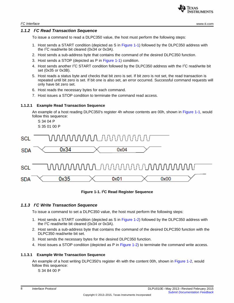
1.1.2.1 Example Read Transaction SequenceAn example of a host reading DLPC350's register 4h whose contents are 00h, shown in Figure 1-1, wouldfollow this sequence:
S 34 04 PS 35 01 00 P
Figure 1-1. I2C Read Register Sequence
1.1.3 I2C Write Transaction SequenceTo issue a command to set a DLPC350 value, the host must perform the following steps:
1. Host sends a START condition (depicted as S in Figure 1-2) followed by the DLPC350 address withthe I2C read/write bit cleared (0x34 or 0x3A).
2. Host sends a sub-address byte that contains the command of the desired DLPC350 function with theDLPC350 read/write bit set.
3. Host sends the necessary bytes for the desired DLPC350 function.4. Host issues a STOP condition (depicted as P in Figure 1-2) to terminate the command write access.
1.1.3.1 Example Write Transaction SequenceAn example of a host writing DLPC350's register 4h with the content 00h, shown in Figure 1-2, wouldfollow this sequence:
S 34 84 00 P
8 Interface Protocol DLPU010E–May 2013–Revised February 2015Submit Documentation Feedback
Copyright © 2013–2015, Texas Instruments Incorporated

www.ti.com USB Interface
Figure 1-2. I2C Write Register Sequence
1.2 USB InterfaceThe DLPC350 controller also supports the USB 1.1 human interface device (HID) to exchange commandsand data with a host processor. The USB commands are variable length data packets that are sent withthe least significant byte first. The DLPC350 offers two different serial numbers for USB enumerationbased on whether the I2C_ADDR_SEL pin is high or low.
1.2.1 USB Transaction SequenceThe USB 1.1 HID protocol has the following structure shown in Figure 1-3:
Figure 1-3. USB HID Protocol
1.2.2 USB Read Transaction SequenceTo issue a command to request a DLPC350 value, the host must perform the following steps:
1. Host sends the Report ID byte, which is set to 0.2. Host sends the Flags byte, where
9DLPU010E–May 2013–Revised February 2015 Interface ProtocolSubmit Documentation Feedback
Copyright © 2013–2015, Texas Instruments Incorporated

USB Interface www.ti.com
• Bits 2:0 are set to 0x0 for regular DLPC350 operation, and 0x7 for debugging assistance• Bit 6 is set to 0x1 to indicate the host wants a reply from the device• Bit 7 is set to 0x1 to indicate a read transaction
3. Host sends the Sequence byte. When a single command is more than 64 bytes, it is sent as multipleUSB packets and the sequence byte is used to number the packets so the device can assemble themin the right sequence. In other cases, this value is irrelevant and generally set to 0.
4. Host sends two bytes with the length of the data packet. This length denotes the number of data bytesin the packet and excludes the number of bytes in steps 1 through 4. It denotes the total number ofbytes sent in steps 5 (command bytes) and 6 (data bytes).
5. Host sends two subcommand bytes: CMD2 and CMD3.6. Host sends data appropriate to command.7. After completion of this command, DLPC350 responds with a packet that includes:
(a) Byte with the command requested by the host (the matching Sequence byte)(b) Length of the data packet(c) Data requested
1.2.3 USB Write Transaction SequenceTo issue a command to set a DLPC350 value, the host must perform the following steps:
1. Host sends the Report ID byte, which is set to 0.2. Host sends the Flags byte, where
• Bits 2:0 are set to 0x0 for regular DLPC350 operation, and 0x7 for debugging assistance• Bit 6 is set to 0x1 to indicate the host wants a reply from the device. This bit needs to be set for
write transactions only if an acknowledgment or reply is needed, which is usually not required.• Bit 7 is set to 0x1 to indicate a read transaction
3. Host sends the Sequence byte. When a single command is more than 64 bytes, it is sent as multipleUSB packets and the sequence byte is used to number the packets so the device can assemble themin the right sequence. In other cases, this value is irrelevant and generally set to 0.
4. Host sends two bytes with the length of the data packet. This length denotes the number of data bytesin the packet and excludes the number of bytes in steps 1 through 4. It denotes the total number ofbytes sent in steps 5 (command bytes) and 6 (data bytes).
5. Host sends two subcommand bytes: CMD2 and CMD3.6. Host sends data appropriate to command.7. After completion of this command, DLPC350 responds with a packet that includes a byte with the
command requested by the host. This occurs only if bit 6 was set in the Flags byte.
10 Interface Protocol DLPU010E–May 2013–Revised February 2015Submit Documentation Feedback
Copyright © 2013–2015, Texas Instruments Incorporated

www.ti.com USB Interface
11DLPU010E–May 2013–Revised February 2015 Interface ProtocolSubmit Documentation Feedback
Copyright © 2013–2015, Texas Instruments Incorporated

Chapter 2DLPU010E–May 2013–Revised February 2015
DLPC350 Control Commands
This chapter lists the DLPC350 control commands.
The following sections list the supported control commands of the DLPC350. In the Type column, ‘wr’ typeis writeable field through I2C or USB write transactions. Data can also be read through I2C or USB readtransactions for ‘wr’ type bits. Type r is read-only. Write transactions to read-only fields are ignored.
The Reset column in all of the following command tables is the default value after power up. These valuesmay be overwritten after power up.
NOTE: Reserved bits and registers. When writing to valid command bit fields, all bits marked asunused or reserved should be set to 0, unless specified otherwise.
NOTE: Momentary Image Corruption During Command Writes. Certain commands may causebrief visual artifacts in the display image under some circumstances. Command data valuesmay always be read without impacting displayed image. To avoid momentary imagecorruption due to a command, disable the LEDs prior to the command write, then reenablethe LEDs after all commands have been issued.
NOTE: Writing or reading from undocumented registers is NOT recommended.
2.1 DLPC350 Status CommandsThe DLPC350 has the following set of status commands:
Hardware StatusSystem StatusMain StatusRetrieve Firmware Version
2.1.1 Hardware Status(I2C: 0x20)
(USB: CMD2: 0x1A, CMD3: 0x0A)
The Hardware Status command provides status information on the DLPC350's sequencer, DMDcontroller, and initialization.
12 DLPC350 Control Commands DLPU010E–May 2013–Revised February 2015Submit Documentation Feedback
Copyright © 2013–2015, Texas Instruments Incorporated

www.ti.com DLPC350 Status Commands
Table 2-1. Hardware Status Register
BYTE BITS DESCRIPTION RESET TYPEInternal Initialization
0 0 = Error b1 r1 = Successful
1 Reserved b0 rDMD Reset Controller Error0 = No error has occurred2 b0 r1 = Multiple overlapping bias or reset operations are accessing the sameDMD block.Forced Swap Error
3 0 = No error has occurred. b0 r01 = Forced Swap Error occurred.
4 Reserved b0 r5 Reserved b0 r
Sequencer Abort Status Flag6 0 = No error has occurred b0 r
1 = Sequencer has detected an error condition that caused an abortSequencer Error
7 0 = No error has occurred. b0 r1 = Sequencer detected an error.
NOTE: Any error condition indicates a fault condition and it must be corrected.
2.1.2 System Status(I2C: 0x21)
(USB: CMD2: 0x1A, CMD3: 0x0B)
The System Status command provides DLPC350 status on internal memory tests.
Table 2-2. System Status Register
BYTE BITS DESCRIPTION RESET TYPEInternal Memory Test
0 0 = Internal Memory Test failed b1 r0
1 = Internal Memory Test passed1:7 Reserved b0 r
2.1.3 Main Status(I2C: 0x22)
(USB: CMD2: 0x1A, CMD3: 0x0C)
The Main Status command provides the status of DMD park and DLPC350 sequencer, frame buffer, andgamma correction.
13DLPU010E–May 2013–Revised February 2015 DLPC350 Control CommandsSubmit Documentation Feedback
Copyright © 2013–2015, Texas Instruments Incorporated

DLPC350 Status Commands www.ti.com
Table 2-3. Main Status Register
BITS BITS DESCRIPTION RESET TYPE0 0 DMD Park Status b0 r
0 = DMD micromirrors are not parked1 = DMD micromirrors are parked
1 Sequencer Run Flag b0 r0 = Sequencer is stopped1 = Sequencer is running normally
2 Frame Buffer Swap Flag b0 r0 = Frame buffer is not frozen1 = Frame buffer is frozen
3 Gamma Correction Function Enable b0 r0 = Gamma correction is disabled1 = Gamma correction is enabled
4:7 Reserved b0 r
2.1.4 Retrieve Firmware Version(I2C: 0x11)
(USB: CMD2: 0x02, CMD3: 0x05)
This command, supported in firmware version 2.0.0 and newer, reads the version information of theDLPC350 firmware.
Table 2-4. Get Version Command
BYTE BITS DESCRIPTION RESET TYPEApplication software revision:
15:0 Application software patch number3:0 x0 r
23:16 Application software minor revision31:24 Application software major revision
API software revision:15:0 API patch number
7:4 x0 r23:16 API minor revision31:24 API major revision
Software configuration revision:15:0 Software configuration patch number
11:8 x0 r23:16 Software configuration minor revision31:24 Software configuration major revision
Sequencer configuration revision:15:0 Sequencer configuration patch number
15:12 x0 r23:16 Sequencer configuration minor revision31:24 Sequencer configuration major revision
2.1.5 Input Video Signal Detection Status(I2C: 0x01)
(USB: 0x04, CMD2: 0x07, CMD3: 0x1C)
14 DLPC350 Control Commands DLPU010E–May 2013–Revised February 2015Submit Documentation Feedback
Copyright © 2013–2015, Texas Instruments Incorporated
www.ti.com DLPC350 Programming Commands
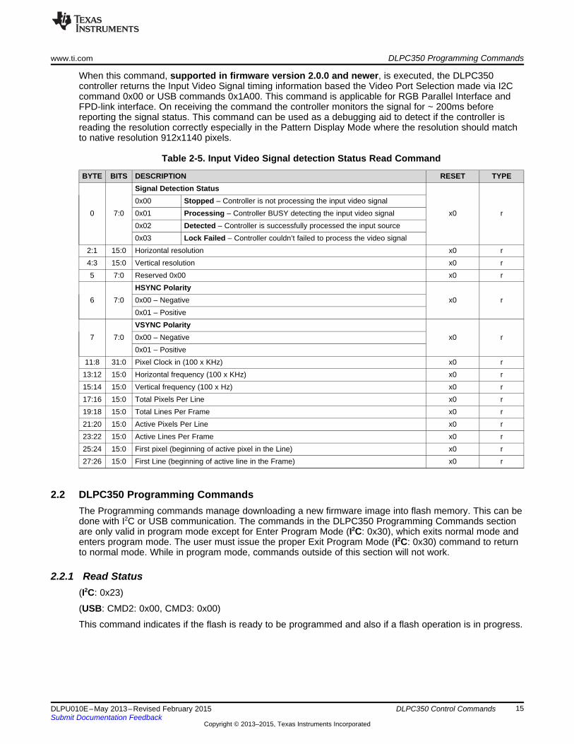
When this command, supported in firmware version 2.0.0 and newer, is executed, the DLPC350controller returns the Input Video Signal timing information based the Video Port Selection made via I2Ccommand 0x00 or USB commands 0x1A00. This command is applicable for RGB Parallel Interface andFPD-link interface. On receiving the command the controller monitors the signal for ~ 200ms beforereporting the signal status. This command can be used as a debugging aid to detect if the controller isreading the resolution correctly especially in the Pattern Display Mode where the resolution should matchto native resolution 912x1140 pixels.
Table 2-5. Input Video Signal detection Status Read Command
BYTE BITS DESCRIPTION RESET TYPESignal Detection Status0x00 Stopped – Controller is not processing the input video signal
0 7:0 0x01 Processing – Controller BUSY detecting the input video signal x0 r0x02 Detected – Controller is successfully processed the input source0x03 Lock Failed – Controller couldn’t failed to process the video signal
2:1 15:0 Horizontal resolution x0 r4:3 15:0 Vertical resolution x0 r5 7:0 Reserved 0x00 x0 r
HSYNC Polarity6 7:0 0x00 – Negative x0 r
0x01 – PositiveVSYNC Polarity
7 7:0 0x00 – Negative x0 r0x01 – Positive
11:8 31:0 Pixel Clock in (100 x KHz) x0 r13:12 15:0 Horizontal frequency (100 x KHz) x0 r15:14 15:0 Vertical frequency (100 x Hz) x0 r17:16 15:0 Total Pixels Per Line x0 r19:18 15:0 Total Lines Per Frame x0 r21:20 15:0 Active Pixels Per Line x0 r23:22 15:0 Active Lines Per Frame x0 r25:24 15:0 First pixel (beginning of active pixel in the Line) x0 r27:26 15:0 First Line (beginning of active line in the Frame) x0 r
2.2 DLPC350 Programming CommandsThe Programming commands manage downloading a new firmware image into flash memory. This can bedone with I2C or USB communication. The commands in the DLPC350 Programming Commands sectionare only valid in program mode except for Enter Program Mode (I2C: 0x30), which exits normal mode andenters program mode. The user must issue the proper Exit Program Mode (I2C: 0x30) command to returnto normal mode. While in program mode, commands outside of this section will not work.
2.2.1 Read Status(I2C: 0x23)
(USB: CMD2: 0x00, CMD3: 0x00)
This command indicates if the flash is ready to be programmed and also if a flash operation is in progress.
15DLPU010E–May 2013–Revised February 2015 DLPC350 Control CommandsSubmit Documentation Feedback
Copyright © 2013–2015, Texas Instruments Incorporated

DLPC350 Programming Commands www.ti.com
Table 2-6. Read Status Command
BYTE BITS DESCRIPTION RESET TYPE2:0 Reserved
Busy Bit3 0 = No flash operation in progress
1 = Flash operation in progress0 d0 r
6:4 ReservedProgramming Mode Bit
7 0 = Does not allow flash programming operations1 = Allows flash programming operations
2.2.2 Enter Program Mode(I2C: 0x30)
(USB: CMD2: 0x30, CMD3: 0x01)
This command tells the controller to enter its programming mode and jump to the boot loader. If the bootloader receives this command, then the command has no effect.
Table 2-7. Enter Program Mode Command
BYTE BITS DESCRIPTION RESET TYPEProgram Mode
00 0 = Enter Program Mode – Jump to boot loader d0 w
7:1 Reserved
2.2.2.1 Exit Program Mode(I2C: 0x30)
(USB: CMD2: 0x00, CMD3: 0x30)
This command tells the controller to exit its programming mode. If the application receives the exitcommand, the command has no effect.
Table 2-8. Exit Program Mode Command
BYTE BITS DESCRIPTION RESET TYPEProgram Mode
00 1 = Exit Program Mode – Reset controller and run application d0 w
7:1 Reserved
2.2.3 Read Control(I2C: 0x15)
(USB: CMD2: 0x00, CMD3: 0x15)
This command reads the Flash Manufacturer and Device IDs, as well as the Checksum, after theCalculate Checksum command is executed.
16 DLPC350 Control Commands DLPU010E–May 2013–Revised February 2015Submit Documentation Feedback
Copyright © 2013–2015, Texas Instruments Incorporated

www.ti.com DLPC350 Programming Commands
Table 2-9. Query Flash IDs Command
BYTE BITS DESCRIPTION RESET TYPEID0 = Returns Checksum
3:00 C = Requests Flash Manufacturer ID d0 r
D = Requests Flash Device ID7:4 Reserved
2.2.4 Start Address(I2C: 0x29)
(USB: CMD2: 0x00, CMD3: 0x29)
The Start Address command specifies the start address for the next flash download. It is the responsibilityof the user to ensure that the Start Address is on a sector boundary in the current flash device. Thiscommand should be followed by a Flash Data Size command and a Flash Erase command to completelydescribe the programming operation.
The start address is also used in specifying the start of a checksum operation
Table 2-10. Start Address Command
BYTE BITS DESCRIPTION RESET TYPE3:0 32:0 Flash address. Byte 0 is LSB, byte 3 is MSB. x0 w
2.2.5 Erase Sector(I2C: 0x28)
(USB: CMD2: 0x00, CMD3: 0x28)
This is a system write command to erase a sector of flash memory. This command should not beexecuted until valid data has been written to the Flash Start Address. Users are responsible for ensuringthat a valid address has been written. The Busy bit will be set in the Boot Loader status byte while thesector erase is in progress.
NOTE: TI cautions against erasing the boot sector of the device as this contains key initializationparameters and the flash programming functionality. Only the sector that contains the startaddress will be erased, not all sectors from the start address to the end of the device. Usersmust either pre-erase all sectors to be programmed, or erase and program each sectorindividually.
2.2.6 Download Data Size(I2C: 0x2C)
(USB: CMD2: 0x00, CMD3: 0x2C)
System write command to specify the size of the following flash download. The data size is sent to tell theBoot Loader how many bytes to expect to program into the flash device during the current operation. It isalso used for specifying the checksum range when requesting that operation.
Table 2-11. Download Data Size Command
BYTE BITS DESCRIPTION RESET TYPE3:0 32:0 Flash address. Byte 0 is LSB, byte 3 is MSB. x0 w
17DLPU010E–May 2013–Revised February 2015 DLPC350 Control CommandsSubmit Documentation Feedback
Copyright © 2013–2015, Texas Instruments Incorporated

DLPC350 Programming Commands www.ti.com
2.2.7 Download Data(I2C: 0x25)
(USB: CMD2: 0x00, CMD3: 0x25)
This command contains the flash data to be programmed. The maximum data size which can be sent ineach command is 512 bytes, which corresponds to a data length of 514. The number of bytes downloadedby consecutive download data commands must match the predefined Flash Data Size for the operation tobe successful.
Table 2-12. Download Data Command
BYTE BITS DESCRIPTION RESET TYPE0 7:0 Length LSB1 7:0 Length MSB
x0 w513:2 4095:0 Up to 512 Data Bytes514 7:0 Checksum
2.2.8 Calculate Checksum(I2C: 0x26)
(USB: CMD2: 0x00, CMD3: 0x26)
This command calculates the checksum. Executing this command causes the Boot Loader to read thedata in the flash memory and calculate a 4-byte 8-bit checksum. The Busy bit will be set in the BootLoader status byte while the checksum computation is in progress. After completion, the 4-byte checksumcan be read back through the Read Control command. The data range to be summed is specified bywriting appropriate data with the Flash Start Address and Flash Data Size commands.
2.3 Chipset Control CommandsThe DLPC350 has the following set of control commands:
Chipset configuration and controlParallel interface configuration and controlInput source controlImage rotation and flip controlImage processing controlLED driver controlSleep mode controlGPIO controlDLP display sequence control
I2C control commands are accepted in any order, except when special sequencing is required (forexample, setting up the flash). Each control command is validated for sub-address and parameter errorsas it is received. Commands failing validation are ignored. On power up, it is necessary to wait forDLPC350 to complete its initialization before sending it any I2C or USB transactions. The INIT_DONE pinsignals when initialization is complete (see the DLPC350 data sheet, DLPS029).
2.3.1 Chipset Configuration and Control CommandsThe Chipset and Configuration Control commands manage software reset, power down modes, bufferfreeze, and image curtain display.
2.3.1.1 Software Reset(I2C: 0x13)
18 DLPC350 Control Commands DLPU010E–May 2013–Revised February 2015Submit Documentation Feedback
Copyright © 2013–2015, Texas Instruments Incorporated

www.ti.com Chipset Control Commands
(USB: CMD2: 0x08, CMD3: 0x02)
This command issues a software reset to the DLPC350, regardless of the argument sent. This commandprovides a back-up recovery mechanism.
Table 2-13. Software Reset Command
BYTE BITS DESCRIPTION RESET TYPESoftware Reset. A set or reset of this bit will perform a software reset:
0 0 0 – No software reset d0 w1 – Perform a software reset
2.3.1.2 Power Control(I2C: 0x07)
(USB: CMD2: 0x02, CMD3: 0x00)
The Power Control places the DLPC350 in a low-power state and powers down the DMD interface.Standby mode should only be enabled after all data for the last frame to be displayed has beentransferred to the DLPC350. Standby mode must be disabled prior to sending any new data. Afterexecuting this command, poll the system status using I2C commands: 0x20, x21, and 0x22 or USBcommands: 0x1A0A, 0x1A0B, and 0x1A0C.
Table 2-14. Interface Sleep Control Command
BYTE BITS DESCRIPTION RESET TYPEPower Control0 = Normal operation. The selected external source will be displayed1:0 d0 wr
0 1 = Standby mode. Places DLPC350 in low-power state and powersdown the DMD interface
7:2 Reserved d0 r
2.3.1.3 Buffer ControlsThe buffer control commands allow buffer swaps, provide the current buffer pointer, and freeze the buffer.
2.3.1.3.1 Force Buffer Swap(I2C: 0x71)
(USB: CMD2: 0x1A, CMD3: 0x26)
The Force Buffer Swap command switches between the two internal memory buffers by swapping theread and write pointers. After a buffer swap, the 24 bit-plane buffer that was streaming data to the DMD isnow used for input, while the previous 24 bit-plane input buffer, now streams data to the DMD. The buffershould be frozen before executing this command.
Table 2-15. Force Buffer Swap Command
BYTE BITS DESCRIPTION RESET TYPEBuffer Swap
0 1 - Swap internal memory buffer pointers d0 wr0
0 - No change to the internal memory buffer pointers7:1 Reserved d0 r
19DLPU010E–May 2013–Revised February 2015 DLPC350 Control CommandsSubmit Documentation Feedback
Copyright © 2013–2015, Texas Instruments Incorporated

Chipset Control Commands www.ti.com
2.3.1.3.2 Display Buffer Freeze(I2C: 0x7C)
(USB: CMD2: 0x10, CMD3: 0x0A)
The Display Buffer Freeze command disables swapping the memory buffers. When reconfiguring thechipset through a series of commands that change the input source or operating mode, TI recommendsthe Display Buffer Swap Freeze command to prevent temporary artifacts from reaching the display. Whenthe display buffer is frozen, the last image streamed to the DMD continues to be displayed.
Table 2-16. Display Buffer Freeze Command
BYTE BITS DESCRIPTION RESET TYPEDisplay Buffer Swap Freeze
0 0 0 - Enable Buffer Swapping d1 wr1 - Disable Buffer Swapping (freeze display buffer)
2.3.1.3.3 Buffer Write Disable(I2C: 0x72)
(USB: CMD2: 0x1A, CMD3: 0x27)
The Buffer Write Disable command prevents the overwriting of the contents of the 48 bit-planes OR two24-bit frame buffers of the internal memory buffer.
Table 2-17. Buffer Write Disable Command
BYTE BITS DESCRIPTION RESET TYPEBuffer Write Disable
0 1 = Disables writes to all the internal memory buffer d0 wr0
0 = Normal operation7:1 Reserved d0 r
2.3.1.3.4 Current Read Buffer Pointer(I2C: 0x73)
(USB: CMD2: 0x1A, CMD3: 0x28)
The Current Read Buffer Pointer command returns the pointer to the current internal memory bufferwhose data is streamed to the DMD.
Table 2-18. Current Buffer Pointer Command
BYTE BITS DESCRIPTION RESET TYPECurrent Read Buffer Pointer Command
0 1 = Buffer number 1 is streaming to DMD d0 wr0
0 = Buffer number 0 is streaming to DMD7:1 Reserved d0 r
2.3.1.4 Display Curtain Control(I2C: 0x06)
(USB: CMD2: 0x11, CMD3: 0x00)
20 DLPC350 Control Commands DLPU010E–May 2013–Revised February 2015Submit Documentation Feedback
Copyright © 2013–2015, Texas Instruments Incorporated

www.ti.com Chipset Control Commands
This register provides image curtain control. When enabled and the input source is set to external videowith no video source connected, a solid color field is displayed on the entire DMD display. The DisplayCurtain Control provides an alternate method of masking temporary source corruption from reaching thedisplay due to on-the-fly reconfiguration. It is also useful for optical test and debug support.
Table 2-19. Display Curtain Control Command
BYTE BITS DESCRIPTION RESET TYPE1:0 9:0 Red color intensity in a scale from 0 to 1023 x0 wr3:2 9:0 Green color intensity in a scale from 0 to 1023 x0 wr5:4 9:0 Blue color intensity in a scale from 0 to 1023 x0 wr
2.3.2 Interface Configuration and ControlThe Interface Configuration and Control manage the operation of the parallel and FPD-link interfaces.
2.3.2.1 Input Data Channel Swap(I2C: 0x04)
(USB: CMD2: 0x1A, CMD3: 0x37)
The Input Data Channel Swap commands configure the specified input data port and map the datasubchannels. The DLPC350 interprets Channel A as Green, Channel B as Red, and Channel C as Blue.
Table 2-20. Input Data Channel Swap Command
BYTE BITS DESCRIPTION RESET TYPESwap Parallel Interface Data Subchannel:0 - ABC = ABC, No swapping of data subchannels1 - ABC = CAB, Data subchannels are right shifted and circularly rotated2 - ABC = BCA, Data subchannels are left shifted and circularly rotated
2:0 3 - ABC = ACB, Data subchannels B and C are swapped x4 wr0 4 - ABC = BAC, Data subchannels A and B are swapped
5 - ABC = CBA, Data subchannels A and C are swapped6 - Reserved7 - Reserved
6:3 Reserved b0 rSpecified Port
7 0 - Parallel interface b0 wr1 - FPD-link interface
2.3.3 FPD-Link Interface Configuration and ControlThe following commands are unique to the FPD-link interface.
2.3.3.1 FPD-Link Mode and Field Select(I2C: 0x05)
(USB: CMD2: 0x1A, CMD3: 0x04)
The FPD-Link Mode and Field Select command configures the FPD-link pixel map, polarity, and signalselect.
21DLPU010E–May 2013–Revised February 2015 DLPC350 Control CommandsSubmit Documentation Feedback
Copyright © 2013–2015, Texas Instruments Incorporated

Chipset Control Commands www.ti.com
Table 2-21. FPD-Link Mode and Field Select Command
BYTE BITS DESCRIPTION RESET TYPEField Signal Select:0 = Map FPD-Link output from CONT1 onto Field Signal for FPD-link interfaceport
2:0 1 = Map FPD-Link output from CONT2 onto Field Signal for FPD-link interface x0 wrport2 = Force 0 onto Field Signal for FPD-link interface port3 = Reserved
0 3 Swap Polarity x1 wr5:4 Reserved x0 r
FPD-link Pixel Mapping Mode (see Table 2-22)0 = Mode 1
7:6 1 =Mode 2 x1 wr2 = Mode 33 =Mode 4
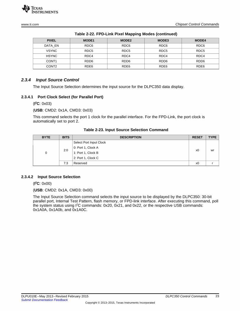
Table 2-22. FPD-Link Pixel Mapping Modes
PIXEL MODE1 MODE2 MODE3 MODE4Green[9] RDB4 RDD3 RDE1 RDB4Green[8] RDB3 RDD2 RDE2 RDB3Green[7] RDB2 RDB4 RDD1 RDB2Green[6] RDB1 RDB3 RDD2 RDB1Green[5] RDB0 RDB2 RDB4 RDB0Green[4] RDA6 RDB1 RDB3 RDA6Green[3] RDD3 RDB0 RDB2 0Green[2] RDD2 RDA6 RDB1 0Green[1] RDE3 RDE3 RDB0 0Green[0] RDE2 RDE2 RDA6 0
Red[9] RDA5 RDD1 RDE1 RDA5Red[8] RDA4 RDD0 RDE0 RDA4Red[7] RDA3 RDA5 RDD1 RDA3Red[6] RDA2 RDA4 RDD0 RDA2Red[5] RDA1 RDA3 RDA5 RDA1Red[4] RDA0 RDA2 RDA4 RDA0Red[3] RDD1 RDA1 RDA3 0Red[2] RDD0 RDA0 RDA2 0Red[1] RDE1 RDE1 RDA1 0Red[0] RDE0 RDE0 RDA0 0
Blue[9] RDC3 RDD5 RDE5 RDC3Blue[8] RDC2 RDD4 RDE4 RDC2Blue[7] RDC1 RDC3 RDD5 RDC1Blue[6] RDC0 RDC2 RDD4 RDC0Blue[5] RDB6 RDC1 RDC3 RDB6Blue[4] RDB5 RDC0 RDC2 RDB5Blue[3] RDD5 RDB6 RDC1 0Blue[2] RDD4 RDB5 RDC0 0Blue[1] RDE5 RDE5 RDB6 0Blue[0] RDE4 RDE4 RDB5 0
22 DLPC350 Control Commands DLPU010E–May 2013–Revised February 2015Submit Documentation Feedback
Copyright © 2013–2015, Texas Instruments Incorporated
www.ti.com Chipset Control Commands
Table 2-22. FPD-Link Pixel Mapping Modes (continued)PIXEL MODE1 MODE2 MODE3 MODE4
DATA_EN RDC6 RDC6 RDC6 RDC6VSYNC RDC5 RDC5 RDC5 RDC5HSYNC RDC4 RDC4 RDC4 RDC4CONT1 RDD6 RDD6 RDD6 RDD6CONT2 RDE6 RDE6 RDE6 RDE6
2.3.4 Input Source ControlThe Input Source Selection determines the input source for the DLPC350 data display.
2.3.4.1 Port Clock Select (for Parallel Port)(I2C: 0x03)
(USB: CMD2: 0x1A, CMD3: 0x03)
This command selects the port 1 clock for the parallel interface. For the FPD-Link, the port clock isautomatically set to port 2.
Table 2-23. Input Source Selection Command
BYTE BITS DESCRIPTION RESET TYPESelect Port Input Clock0: Port 1, Clock A
2:0 x0 wr0 1: Port 1, Clock B
2: Port 1, Clock C7:3 Reserved x0 r
2.3.4.2 Input Source Selection(I2C: 0x00)
(USB: CMD2: 0x1A, CMD3: 0x00)
The Input Source Selection command selects the input source to be displayed by the DLPC350: 30-bitparallel port, Internal Test Pattern, flash memory, or FPD-link interface. After executing this command, pollthe system status using I2C commands: 0x20, 0x21, and 0x22, or the respective USB commands:0x1A0A, 0x1A0b, and 0x1A0C.
23DLPU010E–May 2013–Revised February 2015 DLPC350 Control CommandsSubmit Documentation Feedback
Copyright © 2013–2015, Texas Instruments Incorporated

Chipset Control Commands www.ti.com
Table 2-24. Input Source Selection Command
BYTE BITS DESCRIPTION RESET TYPESelect the input source and interface mode:0 = Parallel interface with 8-bit, 16-bit, 20-bit, 24-bit, or 30-bit RGB or YCrCb dataformats1 = Internal test pattern; I2C command 0x11 is used to select the test pattern2:0 x0 wrtype.2 = Flash. Images are 24-bit single-frame, still images stored in flash that areuploaded on command.3 = FPD-link interface
0 Parallel Interface bit depth0 = 30 bits1 = 24 bits
5:3 2 = 20 bits x1 wr3 = 16 bits4 = 10 bits5 = 8 bits
7:6 Reserved x0 r
2.3.4.3 Input Pixel Data Format(I2C: 0x02)
(USB: CMD2: 0x1A, CMD3: 0x02)
The Input Pixel Data Format command defines the pixel data format input into the DLPC350.
Table 2-25. Input Pixel Data Format Command
BYTE BITS DESCRIPTION RESET TYPESelect the pixel data format: Supported Pixel Formats vs Source Type
Parallel Test Pattern Flash Image FPD-Link3:0 0 - RGB 4:4:4 (30 bit) Yes Yes Yes Yes d0 wr
01 - YCrCb 4:4:4 (30 bit) Yes No No No2 - YCrCb 4:2:2 Yes No Yes No
7:6 Reserved x0 r
2.3.4.4 Internal Test Patterns Select(I2C: 0x0A)
(USB: CMD2: 0x12, CMD3: 0x03)
When the internal test pattern is the selected input, the Internal Test Patterns Select defines the testpattern displayed on the screen. These test patterns are internally generated and injected into thebeginning of the DLPC350 image processing path. Therefore, all image processing is performed on thetest images. All command registers should be set up as if the test images are input from an RGB 8:8:8external source. The resolution of the Test Pattern should be configured with the Input DisplayResolutions commands. Frame Rate should be configured with the Frame Rate commands.
24 DLPC350 Control Commands DLPU010E–May 2013–Revised February 2015Submit Documentation Feedback
Copyright © 2013–2015, Texas Instruments Incorporated

www.ti.com Chipset Control Commands
Table 2-26. Internal Test Patterns Select Command
BYTE BITS DESCRIPTION RESET TYPEInternal Test Patterns Select: x8 wr0x0 = Solid field0x1 = Horizontal ramp0x2 = Vertical ramp0x3 = Horizontal lines0x4 = Diagonal lines
3:00 0x5 = Vertical lines
0x6 = Grid0x7 = Checkerboard0x8 = RGB ramp0x9 = Color bars0xA = Step bars
7:4 Reserved
2.3.4.5 Internal Test Patterns Color Control(I2C: 0x1A)
(USB: CMD2: 0x12, CMD3: 0x04)
When the internal test pattern is the selected input, the Internal Test Patterns Color Control defines thecolors of the test pattern displayed on the screen. These test patterns are internally generated andinjected into the beginning of the DLPC350 image processing path. Therefore, all image processing isperformed on the test images. All command registers should be set up as if the test images are input froman RGB 8:8:8 external source. The foreground color setting affects all test patterns. The background colorsetting affects those test patterns that have a foreground and background component, such as, HorizontalLines, Diagonal Lines, Vertical Lines, Grid, and Checkerboard.
Table 2-27. Internal Test Patterns Color Control Command
BYTE BITS DESCRIPTION RESET TYPERed Foreground Color intensity in a scale from 0 to 10230x0 = No Red Foreground color intensity
1:0 9:0 x3FF wr...0x3FF = Full Red Foreground color intensityGreen Foreground Color intensity in a scale from 0 to 10230x0 = No Green Foreground color intensity
3:2 9:0 x3FF wr...0x3FF = Full Green Foreground color intensityBlue Foreground Color intensity in a scale from 0 to 10230x0 =No Blue Foreground color intensity
5:4 9:0 x3FF wr...0x3FF = Full Blue Foreground color intensityRed Background Color intensity in a scale from 0 to 10230x0 = No Red Background color intensity
7:6 9:0 x0 wr...0x3FF = Full Red Background color intensityGreen Background Color intensity in a scale from 0 to 10230x0 = No Green Background color intensity
9:8 9:0 x0 wr...0x3FF = Full Green Background color intensity
25DLPU010E–May 2013–Revised February 2015 DLPC350 Control CommandsSubmit Documentation Feedback
Copyright © 2013–2015, Texas Instruments Incorporated

Chipset Control Commands www.ti.com
Table 2-27. Internal Test Patterns Color Control Command (continued)BYTE BITS DESCRIPTION RESET TYPE
Blue Background Color intensity in a scale from 0 to 10230x0 = No Blue Background color intensity
11:10 9:0 x0 wr...0x3FF = Full Blue Background color intensity
2.3.4.6 Load Image(I2C: 0x7F)
(USB: CMD2: 0x1A, CMD3: 0x39)
This command loads an image from flash memory and then performs a buffer swap to display the loadedimage on the DMD. After executing this command, poll the system status using I2C commands: 0x20,0x21, and 0x22 or the respective USB commands: 0x1A0A, 0x1A0B, and 0x1A0C.
Table 2-28. Load Image Command
BYTE BITS DESCRIPTION RESET TYPEImage Index. Loads the image at this index. Reading this back provides the index that was0 7:0 x0 wrloaded most recently through this command.
2.3.4.7 Image Load Timing(I2C: 0x61)
(USB: 0x02/0x04, CMD2: 0x1A, CMD3: 0x3A)
When this command is executed, the system will load the image index mentioned in Section 2.3.4.6 andcollect the amount of time it took to load that image. The busy status of the system will be high until theimages have been loaded and the timing information is collected. This command cannot be executedwhile the system is already displaying patterns from flash. After executing this command, poll the systemstatus using I2C commands: 0x20, 0x21, and 0x22 or the respective USB commands: 0x1A0A, 0x1A0B,and 0x1A0C.
Table 2-29. Image Load Timing Write Command
BYTE BITS DESCRIPTION RESET TYPE0 7:0 Starting index of the image for which the timing information is required x0 w1 7:0 Number of images for which the timing information is required x0 w
When reading back the load timing information, the following data format will be received:
Table 2-30. Image Load Timing Read Command
BYTE BITS DESCRIPTION RESET TYPE3:0 31:0 Time taken for image load. Divide this value by 18667 to get the time in milliseconds. x0 r
2.3.4.8 Retrieve Image Resolution Information(I2C: 0x62)
(USB: 0x02/0x04, CMD2: 0x1A, CMD3: 0x41)
26 DLPC350 Control Commands DLPU010E–May 2013–Revised February 2015Submit Documentation Feedback
Copyright © 2013–2015, Texas Instruments Incorporated

www.ti.com Chipset Control Commands
When this command is executed, the system will load the image index mentioned in Section 2.3.4.6 andthe Horizontal and Vertical resolution information of the image(s). The busy status of the system will behigh until the images resolution information is collected. This command cannot be executed while thesystem is already displaying patterns from flash. After executing this command, poll the system statususing I2C commands: 0x20, 0x21, and 0x22 or the respective USB commands: 0x1A0A, 0x1A0B, and0x1A0C.
Table 2-31. Retrieve Image Resolution Information Write Command
BYTE BITS DESCRIPTION RESET TYPE0 7:0 Starting index of the image for which the timing information is required x0 w1 7:0 Number of images for which the timing information is required x0 w
When reading back the load timing information, the following data format will be received:
Table 2-32. Retrieve Image Resolution Information Read Command
BYTE BITS DESCRIPTION RESET TYPE1:0 15:0 Horizontal resolution of 1st image x0 r3:2 15:0 Vertical resolution of 1st image x0 r5:4 15:0 Horizontal resolution of 2nd image x0 r7:6 15:0 Vertical resolution of 2nd image x0 r... ... ... .. ..... ... ... .. ..
N-2:N-3 15:0 Horizontal resolution of Nth image x0 rN:N-1 15:0 Vertical resolution of Nth image x0 r
2.3.5 Image FlipThe DLPC350 supports long- and short-axis image flips to support rear- and front-projection, as well as,table- and ceiling-mounted projection.
NOTE: If showing image from Flash, load image (I2C: 0x7F, USB: 0x1A, 0x39). This must be calledto update the image flip setting.
2.3.5.1 Long-Axis Image Flip:(I2C: 0x08)
(USB: CMD2: 0x10, CMD3: 0x08)
The Long-Axis Image Flip defines whether the input image is flipped across the long axis of the DMD. Ifthis parameter is changed while displaying a still image, the input still image should be re-sent. If theimage is not re-sent, the output image might be slightly corrupted. Figure 2-1 shows an example of a long-axis image flip. In Structured Light mode, the image flip will take effect on the next bit-plane, image, orvideo frame load.
Table 2-33. Long Axis Image Flip Command
BYTE BITS DESCRIPTION RESET TYPEFlips image along the long side of the DMD:
0 0 = Disable flip d0 wr0
1 = Enable flip7:1 Reserved d0 r
27DLPU010E–May 2013–Revised February 2015 DLPC350 Control CommandsSubmit Documentation Feedback
Copyright © 2013–2015, Texas Instruments Incorporated

Flip Disabled Flip EnabledDMD
Flip Disabled Flip EnabledDMD
Chipset Control Commands www.ti.com
Figure 2-1. Image Long-Axis Flip Example
2.3.5.2 Short Axis Image Flip(I2C: 0x09)
(USB: CMD2: 0x10, CMD3: 0x09)
The Short-Axis Image Flip defines whether the input image is flipped across the short axis of the DMD. Ifthis parameter is changed while displaying a still image, the input still image should be resent. If the imageis not re-sent, the output image might be slightly corrupted. Figure 2-2 shows an example of a short axisimage flip. In Structured Light mode, the image flip will take effect on the next bit-plane, image, or videoframe load.
Table 2-34. Short-Axis Image Flip Command
BYTE BITS DESCRIPTION RESET TYPEFlips image along the short side of the DMD:
0 0 - Disable flip d0 wr0
1 - Enable flip7:1 Reserved d0 r
Figure 2-2. Image Short-Axis Flip Example
2.3.6 Image Processing Control
2.3.6.1 Color Space Conversion (CSC)(I2C: 0x26)
(USB: CMD2: 0x1A, CMD3: 0x0D)
The CSC command specifies the color matrix used to translate the input data to RGB data or to colorcorrect the RGB input data. The Color Space Converter contains one color space matrix with nineelements. All nine command bytes must be sent as one contiguous block to ensure that all the coefficientvalues are updated simultaneously.
28 DLPC350 Control Commands DLPU010E–May 2013–Revised February 2015Submit Documentation Feedback
Copyright © 2013–2015, Texas Instruments Incorporated

www.ti.com Chipset Control Commands
Table 2-35. CSC Command
BYTE BITS DESCRIPTION RESET TYPEAttributes of input source:0 - RGB 4:4:4
1:0 d0 wr0 1 - YCrCb 4:4:4
2 - YCrCb 4:2:27:2 Reserved d0 r
RGB 4:4:4 YCrCb 4:4:4 YCrCb 4:2:21 12:0 CSC coefficient 1 x0400 x04A8 x04A8 wr2 12:0 CSC coefficient 2 x0000 xFDC7 xFCC0 wr3 12:0 CSC coefficient 3 x0000 xFF26 xFE6F wr4 12:0 CSC coefficient 4 x0000 x04A8 x04A8 wr5 12:0 CSC coefficient 5 x0400 x0715 x0662 wr6 12:0 CSC coefficient 6 x0000 x0000 x0000 wr7 12:0 CSC coefficient 7 x0000 x04A8 x04A8 wr8 12:0 CSC coefficient 8 x0000 x0000 x0000 wr9 12:0 CSC coefficient 9 x0400 x0875 x0812 wr
Figure 2-3. CSC Matrix
All programmable CSC coefficient values represent numbers less than +4, but greater than or equal to –4.The CSC coefficient values are 13-bit signed 2's complement numbers with the binary point between bits9 and 10 (s2.10 format).
Table 2-36. Color Space Conversion Coefficient Format
Bit 12 Bit 11 Bit 10 Bit 9 Bit 8 Bit 7 Bit 6 Bit 5 Bit 4 Bit 3 Bit 2 Bit 1 Bit 0Sign 21 20 2-1 2-2 2-3 2-4 2-5 2-6 2-7 2-8 2-9 2-10
2.3.7 LED Driver ControlLED driver operation is a function of the individual red, green, and blue LED-enable software-controlparameters. The recommended order for initializing LED drivers is to:1. Program the individual red, green, and blue LED driver currents.2. Program the LED PWM polarity.3. Enable the individual LED enable outputs.4. Turn ON the DLP display sequence (see Section 2.4.1).
The LED-current software-control parameters define PWM values that drive corresponding LED current.The LED enables indicate which LED will be activated.
29DLPU010E–May 2013–Revised February 2015 DLPC350 Control CommandsSubmit Documentation Feedback
Copyright © 2013–2015, Texas Instruments Incorporated

Chipset Control Commands www.ti.com
CAUTIONCareful control of LED current is needed to prevent damage to LEDs. Follow allLED manufacturer recommendations and maintain LED current levels withinrecommended operating conditions. The setting of the LED current depends onmany system and application parameters (including projector thermal design,LED specifications, selected display mode, and so forth). Therefore, therecommended and absolute-maximum settings vary greatly.
2.3.7.1 LED Enable Outputs(I2C: 0x10)
(USB: CMD2: 0x1A, CMD3: 0x07)
The DLPC350 offers three sets of pins to control the LED enables:• LEDR_EN for the red LED• LEDG_EN for the green LED• LEDB_EN for the blue LED
After reset, all LED enables are placed in the inactive state until the board initializes.
Table 2-37. LED Enable Outputs
BYTE BITS DESCRIPTION RESET TYPERed LED Enable
0 0 - Red LED is disabled x0 wr1 - Red LED is enabledGreen LED Enable
1 0 - Green LED is disabled x0 wr1 - Green LED is enabledBlue LED Enable0
2 0 - Blue LED is disabled x0 wr1 - Blue LED is enabledLED Enable Control0 - All LED enables are controlled by bits 2:0 and ignore Sequencer control3 x1 wr1 - All LED enables are controlled by the Sequencer and ignore the settingsin bits 2:0
7:4 Reserved x0 r
2.3.7.1.1 LED PWM Polarity(I2C: 0x0B)
(USB: CMD2: 0x1A, CMD3: 0x05)
The LED PWM Polarity command sets the polarity of all PWM signals. This command must be issuedbefore powering up the LED drivers.
30 DLPC350 Control Commands DLPU010E–May 2013–Revised February 2015Submit Documentation Feedback
Copyright © 2013–2015, Texas Instruments Incorporated

www.ti.com Chipset Control Commands
Table 2-38. LED PWM Polarity Command
BYTE BITS DESCRIPTION RESET TYPEPolarity of PWM signals0 - Normal polarity, PWM 0 value corresponds to no current while PWM
1:0 255 value corresponds to maximum current. x0 wr0
1 - Inverted polarity. PWM 0 value corresponds to maximum current whilePWM 255 value corresponds to no current.
7:2 Reserved x0 r
2.3.7.2 LED Driver Current Control(I2C: 0x4B)
(USB: CMD2: 0x0B, CMD3: 0x01)
This parameter controls the pulse duration of the specific LED PWM modulation output pin. The resolutionis 8 bits and corresponds to a percentage of the LED current. The PWM value can be set from 0 to 100%in 256 steps. If the LED PWM polarity is set to normal polarity, a setting of 0xFF gives the maximum PWMcurrent. The LED current is a function of the specific LED driver design.
CAUTIONCare should be taken when using this command. Improper use of thiscommand can lead to damage to the system. The setting of the LED currentdepends on many system and application parameters (including projectorthermal design, LED specifications, selected display mode, and so forth).Therefore, recommended and absolute-maximum settings vary greatly.
Table 2-39. LED Driver Current Control Command
BYTE BITS DESCRIPTION RESET TYPERed LED PWM current controlValid range, assuming normal polarity of PWM signals, is:0x00 (0% duty cycle → Red LED driver generates no current)
0 7:0 x97 wrto0xFF (100% duty cycle → Red LED driver generates maximum current))The current level corresponding to the selected PWM duty cycle is afunction of the specific LED driver design and thus varies by design.Green LED PWM current controlValid range, assuming normal polarity of PWM signals, is:0x00 (0% duty cycle → Green LED driver generates no current)
1 7:0 x78 wrto0xFF (100% duty cycle → Green LED driver generates maximum current))The current level corresponding to the selected PWM duty cycle is afunction of the specific LED driver design and thus varies by design.Blue LED PWM current controlValid range, assuming normal polarity of PWM signals, is:0x00 (0% duty cycle → Blue LED driver generates no current)
2 7:0 x7D wrto0xFF (100% duty cycle → Blue LED driver generates maximum current))The current level corresponding to the selected PWM duty cycle is afunction of the specific LED driver design and thus varies by design.
31DLPU010E–May 2013–Revised February 2015 DLPC350 Control CommandsSubmit Documentation Feedback
Copyright © 2013–2015, Texas Instruments Incorporated

Chipset Control Commands www.ti.com
2.3.8 GPIO ControlDLPC350 offers 20 general-purpose input/output pins (GPIO). Some of these pins can be configured forPWM output, PWM input, or clock output functionality. By default, all pins are configured as GPIO.
2.3.8.1 GPIO Configuration(I2C: 0x44)
(USB: CMD2: 0x1A, CMD3: 0x38)
The GPIO Configuration command enables GPIO functionality on a specific set of DLPC350 pins. Thecommand sets their direction, output buffer type, and output state.
Table 2-40. GPIO Configuration Command
BYTE BITS DESCRIPTION RESET TYPE0 7:0 GPIO selection. See Table 2-41 for description of available pins n/a wr
1:0 Reserved x0 rInput Value
2 0 = Low x0 r1 = HighOutput State0 = Drive selected GPIO pin low, if the direction is set to output GPIO3 wrdependent1 = Drive selected GPIO pin high, if the direction is set to output and the pin isnot set to open-drain buffer typeOutput Buffer Type
1 GPIO4 0 = Standard buffer (drives high or low) wrdependent1 = Open-drain buffer (drives low only)GPIO Direction
GPIO5 0 = Input wrdependent1 = Output
6 Reserved x0 rGPIO Disable
GPIO7 0 = Enable GPIO wrdependent1 = Disable GPIO (Enable Alternative Function. See Table 2-41.)
Table 2-41. GPIO Selection
GPIO Selection DLPC350 GPIO Pin Function Alternate Function0 GPIO_01 GPIO PWM Output1 Reserved2 GPIO_02 GPIO PWM Output
4:3 Reserved5 GPIO_05 GPIO PWM Input6 GPIO_06 GPIO PWM Input
9:7 Reserved11 GPIO_11 GPIO Clock Out112 GPIO_12 GPIO Clock Out213 GPIO_13 GPIO14 GPIO_14 GPIO15 GPIO_15 GPIO
19:16 Reserved20 GPIO_20 GPIO21 GPIO_21 GPIO
32 DLPC350 Control Commands DLPU010E–May 2013–Revised February 2015Submit Documentation Feedback
Copyright © 2013–2015, Texas Instruments Incorporated

www.ti.com Chipset Control Commands
Table 2-41. GPIO Selection (continued)GPIO Selection DLPC350 GPIO Pin Function Alternate Function
23:22 Reserved24 GPIO_24 GPIO25 GPIO_25 GPIO26 Reserved27 GPIO_27 GPIO28 GPIO_28 GPIO29 GPIO_29 GPIO
32:30 Reserved33 GPIO_33 GPIO34 GPIO_34 GPIO35 GPIO_35 GPIO36 GPIO_36 GPIO
56:37 Reserved
2.3.8.2 GPIO Clock Configuration(I2C: 0x48)
(USB: CMD2: 0x08, CMD3: 0x07)
DLPC350 supports two pins with clock output capabilities: GPIO_11 and GPIO_12. The GPIO ClockConfiguration command enables the clock output functionality and sets the clock frequency.
Table 2-42. GPIO Clock Configuration Command
BYTE BITS DESCRIPTION RESET TYPEClock Selection
1:0 1 = GPIO_11 n/a wr0
2 = GPIO_127:2 Reserved x0 r
Clock Functionality Disable0 0 = Enable clock functionality on selected pin x0 wr
11 = Disable clock functionality on selected pin
7:1 Reserved x0 rClock Divider. Allowed values in the range of 2 to 127. Output frequency =96 MHz / (Clock Divider)0x0 = Reserved0x1 = Reserved
2 7:0 x7F wr0x2 = 2...0x7F = 1270xFF:0x80 = Reserved
2.3.9 Pulse Width Modulated (PWM) ControlDLPC350 provides two general-purpose PWM channels that can be used for a variety of controlapplications, such as fan speed. If the PWM functionality is not needed, these signals can be programmedas GPIO pins. To enable the PWM signals:1. Disable GPIO functionality using the GPIO Configuration command.2. Program the PWM signal using the PWM Setup command.
33DLPU010E–May 2013–Revised February 2015 DLPC350 Control CommandsSubmit Documentation Feedback
Copyright © 2013–2015, Texas Instruments Incorporated

Chipset Control Commands www.ti.com
3. Enable the PWM signal with the PWM Enable command.
2.3.9.1 PWM Setup(I2C: 0x41)
(USB: CMD2: 0x1A, CMD3: 0x11)
The PWM Setup command sets the clock period and duty cycle of the specified PWM channel. The PWMfrequency and duty cycle is derived from an internal 18.67-MHz clock. To calculate the desired PWMperiod, divide the desired clock frequency from the internal 18.67Mhz clock. For example, a PWMfrequency of 2 kHz, requires a 18666667 / 2000 = 9333 or 0x2475. Thus, Byte1 is programmed to 0x24and Byte3 is programmed to 0x75.
Table 2-43. PWM Setup Command
BYTE BITS DESCRIPTION RESET TYPE4:0 Reserved x0 r
PWM Channel Select0 - PWM channel 0 (GPIO_0)
07:5 1 - Reserved x0 wr
2 - PWM channel 2 (GPIO_2)3-7 - ReservedClock Period in increments of 53.57 ns. Clock Period = (value + 1) × 53.5 Channel4:1 31:0 wrns dependentDuty Cycle = (value + 1)% Value range is 1% to 99% Channel6:0 wrdependent5
7 Reserved x0 r
2.3.10 PWM Enable(I2C: 0x40)
(USB: CMD2: 0x1A, CMD3: 0x10)
After the PWM Setup command configures the clock period and duty cycle, the PWM Enable commandactivates the PWM signals.
Table 2-44. PWM Enable Command
BYTE BITS DESCRIPTION RESET TYPEPWM Channel Select0 - PWM channel 0 (GPIO_0)
2:0 n/a wr1 - Reserved2 - PWM channel 2 (GPIO_2)
06:3 Reserved x0 r
PWM Channel Enable Channel 2Enabled0 -Disable selected PWM Channel7 wrChannel 0
1 - Enable selected PWM Channel Disabled
2.3.11 PWM Capture Configuration(I2C: 0x43)
(USB: CMD2: 0x1A, CMD3: 0x12)
The PWM Capture Configuration command samples the specified PWM input signals and returns thePWM clock period in a 4 byte packet.
34 DLPC350 Control Commands DLPU010E–May 2013–Revised February 2015Submit Documentation Feedback
Copyright © 2013–2015, Texas Instruments Incorporated
www.ti.com Chipset Control Commands
Table 2-45. PWM Capture Configuration Command
BYTE BITS DESCRIPTION RESET TYPEPWM Capture Port
0 0 - PWM Input channel 0 (GPIO_5) n/a wr0
1 - PWM Input channel 1 (GPIO_6)7:1 Reserved x0 r
PWM Sample Rate (285 Hz to 18666667 Hz) Port4:1 24:0 wrDependentSample Rate = Pulse Frequency / Duty Cycle
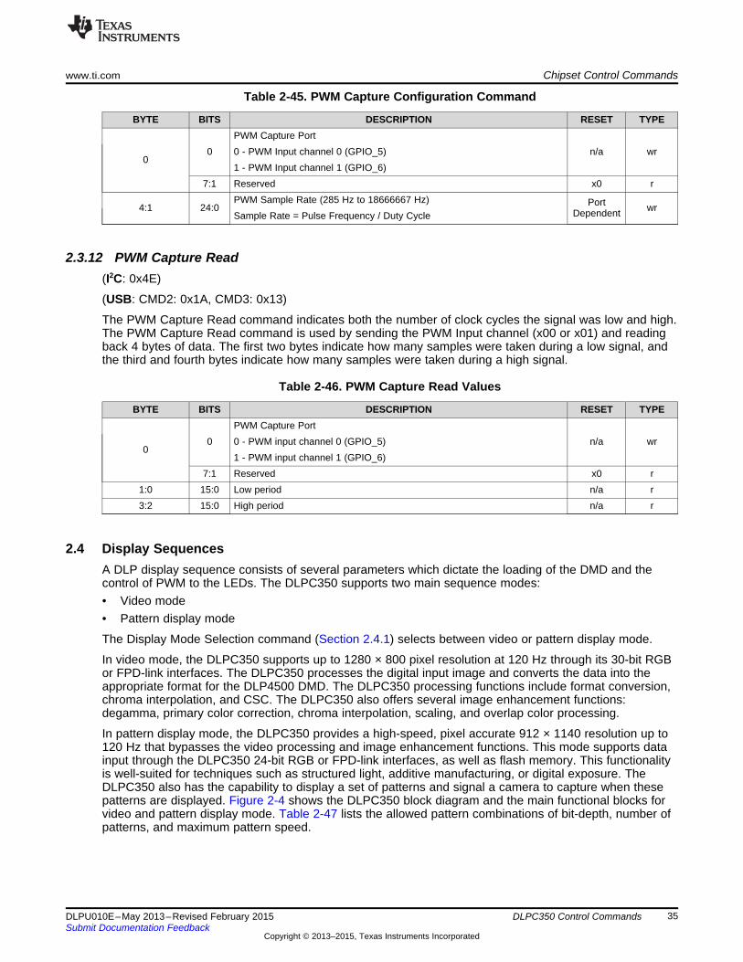
2.3.12 PWM Capture Read(I2C: 0x4E)
(USB: CMD2: 0x1A, CMD3: 0x13)
The PWM Capture Read command indicates both the number of clock cycles the signal was low and high.The PWM Capture Read command is used by sending the PWM Input channel (x00 or x01) and readingback 4 bytes of data. The first two bytes indicate how many samples were taken during a low signal, andthe third and fourth bytes indicate how many samples were taken during a high signal.
Table 2-46. PWM Capture Read Values
BYTE BITS DESCRIPTION RESET TYPEPWM Capture Port
0 0 - PWM input channel 0 (GPIO_5) n/a wr0
1 - PWM input channel 1 (GPIO_6)7:1 Reserved x0 r
1:0 15:0 Low period n/a r3:2 15:0 High period n/a r
2.4 Display SequencesA DLP display sequence consists of several parameters which dictate the loading of the DMD and thecontrol of PWM to the LEDs. The DLPC350 supports two main sequence modes:• Video mode• Pattern display mode
The Display Mode Selection command (Section 2.4.1) selects between video or pattern display mode.
In video mode, the DLPC350 supports up to 1280 × 800 pixel resolution at 120 Hz through its 30-bit RGBor FPD-link interfaces. The DLPC350 processes the digital input image and converts the data into theappropriate format for the DLP4500 DMD. The DLPC350 processing functions include format conversion,chroma interpolation, and CSC. The DLPC350 also offers several image enhancement functions:degamma, primary color correction, chroma interpolation, scaling, and overlap color processing.
In pattern display mode, the DLPC350 provides a high-speed, pixel accurate 912 × 1140 resolution up to120 Hz that bypasses the video processing and image enhancement functions. This mode supports datainput through the DLPC350 24-bit RGB or FPD-link interfaces, as well as flash memory. This functionalityis well-suited for techniques such as structured light, additive manufacturing, or digital exposure. TheDLPC350 also has the capability to display a set of patterns and signal a camera to capture when thesepatterns are displayed. Figure 2-4 shows the DLPC350 block diagram and the main functional blocks forvideo and pattern display mode. Table 2-47 lists the allowed pattern combinations of bit-depth, number ofpatterns, and maximum pattern speed.
35DLPU010E–May 2013–Revised February 2015 DLPC350 Control CommandsSubmit Documentation Feedback
Copyright © 2013–2015, Texas Instruments Incorporated

Display Sequences www.ti.com
Figure 2-4. DLPC350 Functional Block Diagram
Table 2-47. Allowed Pattern Display Combinations
MAXIMUM NUMBER OFMAXIMUM EXTERNAL INPUT MAXIMUM PATTERN RATE FORBIT-DEPTH PATTERNS FOR PRE-LOADEDPATTERN RATE PRE-LOADED PATTERNS PATTERNS1 2880 4225 482 1428 1428 243 636 636 164 588 588 125 480 500 86 400 400 87 222 222 68 120 120 6
The video output modes operate on a per-frame basis where the DLPC350 takes the input data andappropriately allocates it in a frame. For example, a 24-bit RGB input image is allocated into a 60-Hzframe by dividing each color (red, green, and blue) into specific percentages of the frame (see Figure 2-5).Therefore, for 40% red, 45% green, and 15% blue ratio; the red, green, and blue colors have a 6.67-, 7.5-,and 2.54-ms time slot allocated, respectively. Because each color has an 8-bit depth, each color time slotis further divided into bit-planes, as shown in Figure 2-5. A bit-plane is the two-dimensional arrangementof one bit extracted from all the pixels in the full color 2D image.
36 DLPC350 Control Commands DLPU010E–May 2013–Revised February 2015Submit Documentation Feedback
Copyright © 2013–2015, Texas Instruments Incorporated

www.ti.com Display Sequences
Figure 2-5. Bit-Planes of a 24-Bit RGB Image
The length of each bit-plane in the time slot is weighted by the corresponding power of 2 of its binaryrepresentation. This provides a binary pulse-width modulation of the image. In the 24-bit RGB streaminginput, Figure 2-6 shows that each color time slot is divided into eight bit-planes. The sum of all bit weighsin the color time slot equal 255, with each bit-plane weighted by its binary representation.
Figure 2-6. Bit Partition in a Frame for an 8-Bit Monochrome Image
Therefore, a single video frame is composed of a series of bit-planes. Because the DMD mirrors can beeither on or off, an image is created by turning on the mirrors corresponding to the bit set in a bit-planeand shining light on them. With the binary pulse-width modulation, the intensity level of the color isreproduced by controlling the amount of time the mirror is on and illuminated. For a 24-bit RGB frameimage input to the DLPC350, the DLPC350 creates 24 bit-planes, stores them on the internal memorybuffer, and sends them to the DLP4500 DMD on the next frame, one bit-plane at a time. Depending on thebit weight of the bit-plane, the DLPC350 controls the time this bit-plane is exposed to light. The time a bitplane is illuminated is directly proportional to the intensity of the bit-plane. To improve image quality invideo frames, these bit-planes, time slots, and color frames are intertwined and interleaved with spatial-temporal algorithms by the DLPC350.
For other applications where this image enhancement is not desired, the video processing algorithms canbe bypassed and replaced with a specific set of bit-planes. The bit-depth of the pattern is then allocatedinto the corresponding binary weighted time slots. Furthermore, output trigger signals are alsosynchronized with these time slots to indicate when the image is displayed. For structured lightapplications, this mechanism provides the capability to display a set of patterns and signal a camera tocapture these patterns overlaid on an object.
As shown in Figure 2-7, the DLPC350 stores two 24-bit frames in its internal memory buffer. This 48 bit-plane display buffer allows the DLPC350 to send one 24-bit buffer to the DMD array while the secondbuffer is filled from flash or streamed in through the 24-bit RGB interface. In streaming mode, the DMDarray displays the previous 24-bit frame while the current frame fills the second 24-bit frame of the displaybuffer. After a 24-bit frame is displayed, the buffer rotates accessing the next 24-bit frame to the DMD.Thus, the displayed image is a 24-bit frame behind the data streamed through the 24-bit RGB parallelinterface.
37DLPU010E–May 2013–Revised February 2015 DLPC350 Control CommandsSubmit Documentation Feedback
Copyright © 2013–2015, Texas Instruments Incorporated

Display Sequences www.ti.com
Figure 2-7. DLP4500 Frame Buffer
Note that the displayed image is frame delayed in relation to the data streamed through the 24-bit RGBparallel bus, as shown in Figure 2-8.
Figure 2-8. Frame Delay Between RGB Input and Video Output
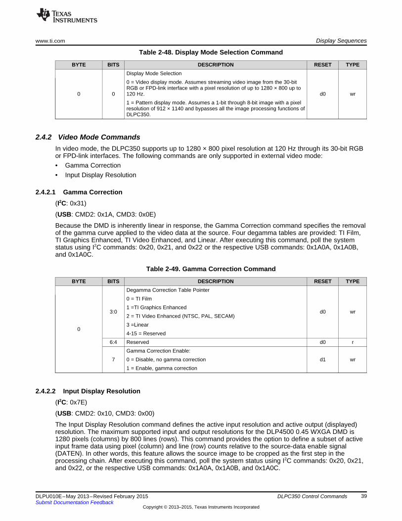
2.4.1 Display Mode Selection Command(I2C: 0x69)
(USB: CMD2: 0x1A, CMD3: 0x1B)
The Display Mode Selection Command enables the DLPC350 internal image processing functions forvideo mode or bypasses them for pattern display mode. This command selects between video or patterndisplay mode of operation. After executing this command, poll the system status using I2C commands:0x20, 0x21, and 0x22 or the respective USB commands: 0x1A0A, 0x1A0B, and 0x1A0C.
38 DLPC350 Control Commands DLPU010E–May 2013–Revised February 2015Submit Documentation Feedback
Copyright © 2013–2015, Texas Instruments Incorporated
www.ti.com Display Sequences
Table 2-48. Display Mode Selection Command
BYTE BITS DESCRIPTION RESET TYPEDisplay Mode Selection0 = Video display mode. Assumes streaming video image from the 30-bitRGB or FPD-link interface with a pixel resolution of up to 1280 × 800 up to
0 0 120 Hz. d0 wr1 = Pattern display mode. Assumes a 1-bit through 8-bit image with a pixelresolution of 912 × 1140 and bypasses all the image processing functions ofDLPC350.
2.4.2 Video Mode CommandsIn video mode, the DLPC350 supports up to 1280 × 800 pixel resolution at 120 Hz through its 30-bit RGBor FPD-link interfaces. The following commands are only supported in external video mode:• Gamma Correction• Input Display Resolution
2.4.2.1 Gamma Correction(I2C: 0x31)
(USB: CMD2: 0x1A, CMD3: 0x0E)
Because the DMD is inherently linear in response, the Gamma Correction command specifies the removalof the gamma curve applied to the video data at the source. Four degamma tables are provided: TI Film,TI Graphics Enhanced, TI Video Enhanced, and Linear. After executing this command, poll the systemstatus using I2C commands: 0x20, 0x21, and 0x22 or the respective USB commands: 0x1A0A, 0x1A0B,and 0x1A0C.
Table 2-49. Gamma Correction Command
BYTE BITS DESCRIPTION RESET TYPEDegamma Correction Table Pointer0 = TI Film1 =TI Graphics Enhanced
3:0 d0 wr2 = TI Video Enhanced (NTSC, PAL, SECAM)3 =Linear
04-15 = Reserved
6:4 Reserved d0 rGamma Correction Enable:
7 0 = Disable, no gamma correction d1 wr1 = Enable, gamma correction
2.4.2.2 Input Display Resolution(I2C: 0x7E)
(USB: CMD2: 0x10, CMD3: 0x00)
The Input Display Resolution command defines the active input resolution and active output (displayed)resolution. The maximum supported input and output resolutions for the DLP4500 0.45 WXGA DMD is1280 pixels (columns) by 800 lines (rows). This command provides the option to define a subset of activeinput frame data using pixel (column) and line (row) counts relative to the source-data enable signal(DATEN). In other words, this feature allows the source image to be cropped as the first step in theprocessing chain. After executing this command, poll the system status using I2C commands: 0x20, 0x21,and 0x22, or the respective USB commands: 0x1A0A, 0x1A0B, and 0x1A0C.
39DLPU010E–May 2013–Revised February 2015 DLPC350 Control CommandsSubmit Documentation Feedback
Copyright © 2013–2015, Texas Instruments Incorporated

Display Sequences www.ti.com
Table 2-50. Input Display Resolution Command
BYTE BITS DESCRIPTION RESET TYPE1:0 15:0 Input image, first active pixel (column) of cropped area d0 wr3:2 15:0 Input image, first active line (row) of cropped area d0 wr
Input image vertical resolution, pixels (columns) per line (row) of cropped5:4 15:0 d0 wrarea7:6 15:0 Input image horizontal resolution, lines (rows) per frame of cropped area d0 wr9:8 15:0 Output image, first active pixel (column) of displayed image d0 wr
11:10 15:0 Output image, first active line (row) of displayed image d0 wr13:12 15:0 Output image horizontal resolution, pixels (columns) per line (row) d1280 wr15:14 15:0 Output image vertical resolution, lines (rows) per frame d800 wr
2.4.3 Pattern Display CommandsIn pattern display mode, the DLPC350 supports 1-, 2-, 3-, 4-, 5-, 6-, 7-, and 8-bit images with a 912 ×1140 pixel resolution streamed through the 24-bit RGB or FPD-link interface, or stored in the flashmemory locations. The following commands are only supported in pattern display mode:
• Validate Data• Trigger Controls• LED Enable Delay Controls• Pattern Display Controls• Exposure Controls• Buffer Controls
NOTE: If the pattern display is already active, it must be stopped using I2C command 0x65 beforemaking the change.
NOTE: Any changes in the setting should be validated using the Validate Data Command
(I2C: 0x7D)
(USB: CMD2: 0x1A, CMD3: 0x1A).
2.4.3.1 Validate Data Command Response(I2C: 0x7D)
(USB: CMD2: 0x1A, CMD3: 0x1A)
The Validate Data command checks the programmed pattern display modes and indicates any invalidsettings. To execute the command, write a dummy byte followed by a one byte read. The byte readcontains the status byte. This command needs to be executed after all pattern display configurations havebeen completed.
40 DLPC350 Control Commands DLPU010E–May 2013–Revised February 2015Submit Documentation Feedback
Copyright © 2013–2015, Texas Instruments Incorporated

www.ti.com Display Sequences
Table 2-51. Validate Data Command Response
BYTE BITS DESCRIPTION RESET TYPEValidity of exposure or frame period settings
0 1 = Selected exposure or frame period settings are invalid d0 r0 = Selected exposure or frame period settings are validValidity of pattern numbers in lookup table (LUT)
1 1 = Selected pattern numbers in LUT are invalid d0 r0 = Selected pattern numbers in LUT are validStatus of Trigger Out1
2 1 = Warning, continuous Trigger Out1 request or overlapping black sectors d0 r0 = Trigger Out1 settings are valid
0 Status of post sector settings3 1 = Warning, post vector was not inserted prior to external triggered vector d0 r
0 = Post vector settings are validStatus of frame period and exposure difference
4 1 = Warning, frame period or exposure difference is less than 230usec0 = Frame period or exposure difference is valid
d0 r6:5 Reserved1 = DLPC350 is busy validating, once it is cleared, then, you can interpretthe rest of the bits70 = DLPC350 has validated, the rest of the bits are ready to be interpreted
NOTE: Poll or read the response byte. Data to be interpreted only when bit 7 goes from 1 to 0.
2.4.3.2 Trigger ControlsTo synchronize a camera with the displayed patterns, the DLPC350 supports three trigger modes:• Trigger Mode 0 (applicable when pattern data from RGB parallel port OR FPD port):
– VSYNC used as trigger input.– TRIG_OUT1 frames the exposure time of the pattern.– TRIG_OUT2 indicates the start of the pattern sequence or internal buffer boundary of a 24-bit
plane.• Trigger Mode 1 (applicable for pattern data from flash):
– TRIG_IN1 advances to next pattern, while TRIG_IN2 starts and pauses the pattern sequence.– TRIG_OUT1 frames the exposure time of the pattern.– TRIG_OUT2 indicates the start of the pattern sequence or internal buffer boundary of a 24-bit
plane.• Trigger Mode 2 (applicable for pattern data from flash):
– TRIG_IN1 toggles between two consecutive patterns– TRIG_IN2 advances to the next pair of patterns– TRIG_OUT1 frames the exposure time of the pattern.– TRIG_OUT2 indicates the start of the pattern sequence or internal buffer boundary of a 24-bit
plane.
41DLPU010E–May 2013–Revised February 2015 DLPC350 Control CommandsSubmit Documentation Feedback
Copyright © 2013–2015, Texas Instruments Incorporated

Display Sequences www.ti.com
Figure 2-9 shows an example of Trigger Mode 0, where the VSYNC starts the pattern sequence display.Frame time indicates the time between VSYNC triggers, and display time indicates the length of patternsequence. This display time should be less than the frame time. The pattern sequence consists of a seriesof three consecutive patterns. The first pattern sequence consists of P1, P2, and P3. Since P3 is an RGBpattern, it is shown with its time sequential representation of P3.1, P3.2, and P3.3. The second patternsequence consists of three patterns: P4, P5, and P6. The third sequence consists of P7, P8, and P9.TRIG_OUT_1 frames each pattern exposed, while TRIG_OUT_2 indicates the start of each of the threepattern sequences. See Section 4.2 for detailed steps on how to generate this pattern sequence.
Figure 2-9. Trigger Mode 0 Timing Diagram Example
Figure 2-10 shows an example of Trigger Mode 1. A set of three-pattern sequences are displayed.TRIG_OUT_1 frames each pattern exposed, while TRIG_OUT_2 indicates the start of each three-patternsequence. TRIG_IN_2 serves as a start/stop signal. By raising TRIG_IN_2, the pattern sequence starts.By lowering TRIG_IN_2, the pattern sequence stops. If the pattern sequence had been previously started,raising TRIG_IN_2 continues the pattern sequence until this signal is lowered. If TRIG_IN_2 is loweredwhile a pattern is displayed (see P4 in Figure 2-10), when this pattern sequence is continued, this patternis displayed again since its full exposure was not completed.
Figure 2-10. Trigger Mode 1 Timing Diagram Example
An example of trigger mode 2 is shown in Figure 2-11, where TRIG_IN_1 alternates between two patternswhile TRIG_IN_2 advances to the next pair of patterns. Table 2-69 shows the allowed patterncombinations in relation to the bit depth of the pattern.
42 DLPC350 Control Commands DLPU010E–May 2013–Revised February 2015Submit Documentation Feedback
Copyright © 2013–2015, Texas Instruments Incorporated

www.ti.com Display Sequences
Figure 2-11. Trigger Mode 2 Timing Diagram Example
2.4.3.2.1 Pattern Trigger Mode Selection(I2C: 0x70)
(USB: CMD2: 0x1A, CMD3: 0x23)
The Pattern Trigger Mode Selection command selects between one of the three Pattern Trigger Modes.Before executing this command, stop the current pattern sequence. After executing this command, sendthe Validation command (I2C: 0x7D or USB: 0x1A1A) once before starting the pattern sequence.
Table 2-52. Pattern Trigger Mode Selection Command
BYTE BITS DESCRIPTION RESET TYPEPattern Trigger Mode Selection0 = Pattern Trigger Mode 0: VSYNC serves to trigger the pattern displaysequence1 = Pattern Trigger Mode 1: Internally or externally (through TRIG_IN_1 andTRIG_IN_2) generated trigger2 = Pattern Trigger Mode 2: TRIG_IN_1 alternates between two patterns,
2:0 d1 wrwhile TRIG_IN_2 advances to the next pair of patterns03 = Pattern Trigger Mode 3: Internally or externally generated trigger forVariable Exposure display sequence.This trigger mode follows the same timing diagram as in Figure 2-10.4 = Pattern Trigger Mode 4: VSYNC triggered for Variable Exposure displaysequence.This trigger mode follows the same timing diagram as in Figure 2-9.
7:3 Reserved d0 r
2.4.3.2.2 Trigger Out1 Control(I2C: 0x6A)(USB: CMD2: 0x1A, CMD3: 0x1D)
The Trigger Out1 Control command sets the polarity, rising edge delay, and falling edge delay of theDLPC350's TRIG_OUT_1 signal. The delays are compared to when the pattern is displayed on the DMD.Before executing this command, stop the current pattern sequence. After executing this command, sendthe Validation command (I2C: 0x7D or USB: 0x1A1A) once before starting the pattern sequence.
43DLPU010E–May 2013–Revised February 2015 DLPC350 Control CommandsSubmit Documentation Feedback
Copyright © 2013–2015, Texas Instruments Incorporated

Display Sequences www.ti.com
Table 2-53. Trigger Out1 Control Command
BYTE BITS DESCRIPTION RESET TYPE0 Reserved d0 r
TRIG_OUT_1 Polarity0 1 1 = Invert TRIG_OUT_1 polarity to an active low signal d0 wr
0 = Normal TRIG_OUT_1 polarity, active high signal7:2 Reserved d0 r
TRIG_OUT_1 rising edge delay control with range -20.05 µs to +2.787 µs.Each bit adds 107.2 ns0x00 = -20.05 µs0x01 = -19.9428 µs0x02 = -19.835 µs
1 7:0 xBB wr..0xBB = 0.00 µs (default)...0xD4 =+2.68 µs0xD5 = +2.787 µsTRIG_OUT_1 falling edge delay control with range -20.05µs to +2.787µs.Each bit adds 107.2 ns0x00 = -20.05 µs0x01 = –19.9428 µs0x02 = –19.835 µs
2 7:0 xBB wr..0xBB = 0.00 µs (default)...0xD4 = +2.68 µs0xD5 = +2.787 µs
2.4.3.2.3 Trigger Out2 Control(I2C: 0x6B)
(USB: CMD2: 0x1A, CMD3: 0x1E)
The Trigger Out2 Control command sets the polarity and rising edge delay of the DLPC350'sTRIG_OUT_2 signal. The delay is compared to when the pattern is displayed on the DMD. Beforeexecuting this command, stop the current pattern sequence. After executing this command, send theValidation command (I2C: 0x7D or USB: 0x1A1A) once before starting the pattern sequence.
Table 2-54. Trigger Out2 Control Command
BYTE BITS DESCRIPTION RESET TYPE0 Reserved d0 r
TRIG_OUT_2 Polarity0 1 1 = Invert TRIG_OUT_2 polarity to an active low signal d0 wr
0 = Normal TRIG_OUT_2 polarity, active high signal7:2 Reserved d0 r
44 DLPC350 Control Commands DLPU010E–May 2013–Revised February 2015Submit Documentation Feedback
Copyright © 2013–2015, Texas Instruments Incorporated
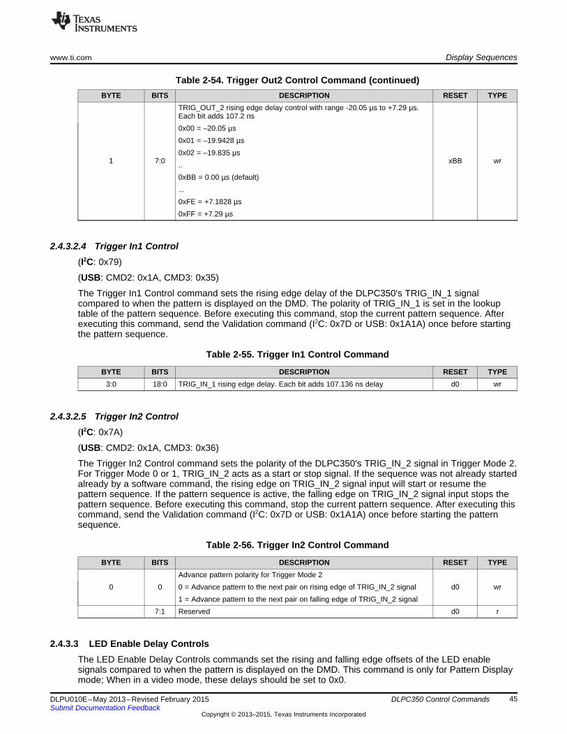
www.ti.com Display Sequences
Table 2-54. Trigger Out2 Control Command (continued)BYTE BITS DESCRIPTION RESET TYPE
TRIG_OUT_2 rising edge delay control with range -20.05 µs to +7.29 µs.Each bit adds 107.2 ns0x00 = –20.05 µs0x01 = –19.9428 µs0x02 = –19.835 µs
1 7:0 xBB wr..0xBB = 0.00 µs (default)...0xFE = +7.1828 µs0xFF = +7.29 µs
2.4.3.2.4 Trigger In1 Control(I2C: 0x79)
(USB: CMD2: 0x1A, CMD3: 0x35)
The Trigger In1 Control command sets the rising edge delay of the DLPC350's TRIG_IN_1 signalcompared to when the pattern is displayed on the DMD. The polarity of TRIG_IN_1 is set in the lookuptable of the pattern sequence. Before executing this command, stop the current pattern sequence. Afterexecuting this command, send the Validation command (I2C: 0x7D or USB: 0x1A1A) once before startingthe pattern sequence.
Table 2-55. Trigger In1 Control Command
BYTE BITS DESCRIPTION RESET TYPE3:0 18:0 TRIG_IN_1 rising edge delay. Each bit adds 107.136 ns delay d0 wr
2.4.3.2.5 Trigger In2 Control(I2C: 0x7A)
(USB: CMD2: 0x1A, CMD3: 0x36)
The Trigger In2 Control command sets the polarity of the DLPC350's TRIG_IN_2 signal in Trigger Mode 2.For Trigger Mode 0 or 1, TRIG_IN_2 acts as a start or stop signal. If the sequence was not already startedalready by a software command, the rising edge on TRIG_IN_2 signal input will start or resume thepattern sequence. If the pattern sequence is active, the falling edge on TRIG_IN_2 signal input stops thepattern sequence. Before executing this command, stop the current pattern sequence. After executing thiscommand, send the Validation command (I2C: 0x7D or USB: 0x1A1A) once before starting the patternsequence.
Table 2-56. Trigger In2 Control Command
BYTE BITS DESCRIPTION RESET TYPEAdvance pattern polarity for Trigger Mode 2
0 0 0 = Advance pattern to the next pair on rising edge of TRIG_IN_2 signal d0 wr1 = Advance pattern to the next pair on falling edge of TRIG_IN_2 signal
7:1 Reserved d0 r
2.4.3.3 LED Enable Delay ControlsThe LED Enable Delay Controls commands set the rising and falling edge offsets of the LED enablesignals compared to when the pattern is displayed on the DMD. This command is only for Pattern Displaymode; When in a video mode, these delays should be set to 0x0.
45DLPU010E–May 2013–Revised February 2015 DLPC350 Control CommandsSubmit Documentation Feedback
Copyright © 2013–2015, Texas Instruments Incorporated

Display Sequences www.ti.com
2.4.3.3.1 Red LED Enable Control(I2C: 0x6C)
(USB: CMD2: 0x1A, CMD3: 0x1F)
The Red LED Enable Delay Control command sets the rising and falling edge delay of the Red LEDenable signal.
Table 2-57. Red LED Enable Control Command
BYTE BITS DESCRIPTION RESET TYPERed LED enable rising edge delay control with range -20.05 µs to +7.29 µs.Each bit adds 107.2 ns0x00 = –20.05 µs0x01 = –19.9428 µs0x02 = –19.835 µs
0 7:0 xBB wr..0xBB = 0.00 µs (default)...0xFE = +7.1828 µs0xFF = +7.29 µsRed LED enable falling edge delay control with range -20.05 µs to +7.29 µs.Each bit adds 107.2 ns0x00 = –20.05 µs0x01 = –19.9428 µs0x02 = –19.835 µs
1 7:0 xBB wr..0xBB = 0.00 µs (default)...0xFE = +7.1828 µs0xFF = +7.29 µs
2.4.3.3.2 Green LED Enable Control(I2C: 0x6D)
(USB: CMD2: 0x1A, CMD3: 0x20)
The Green LED Enable Delay Control command sets the rising and falling edge delay of the Green LEDenable signal.
Table 2-58. Green LED Enable Control Command
BYTE BITS DESCRIPTION RESET TYPEGreen LED enable rising edge delay control with range -20.05 µs to +7.29µs. Each bit adds 107.2 ns0x00 = –20.05 µs0x01 = –19.9428 µs0x02 = –19.835 µs
0 7:0 xBB wr..0xBB = 0.00 µs (default)...0xFE = +7.1828 µs0xFF = +7.29 µs
46 DLPC350 Control Commands DLPU010E–May 2013–Revised February 2015Submit Documentation Feedback
Copyright © 2013–2015, Texas Instruments Incorporated

www.ti.com Display Sequences
Table 2-58. Green LED Enable Control Command (continued)BYTE BITS DESCRIPTION RESET TYPE
Green LED enable falling edge delay control with range -20.05 µs to +7.29µs. Each bit adds 107.2 ns0x00 = –20.05 µs0x01 = –19.9428 µs0x02 = –19.835 µs
1 7:0 xBB wr..0xBB = 0.00 µs (default)...0xFE = +7.1828 µs0xFF = +7.29 µs
2.4.3.3.3 Blue LED Enable Control(I2C: 0x6E)
(USB: CMD2: 0x1A, CMD3: 0x21)
The Blue LED Enable Delay Control command sets the rising and falling edge delay of the Blue LEDenable signal.
Table 2-59. Blue LED Enable Control Command
BYTE BITS DESCRIPTION RESET TYPEBlue LED enable rising edge delay control with range -20.05 µs to +7.29 µs.Each bit adds 107.2 ns0x00 = –20.05 µs0x01 = –19.9428 µs0x02 = –19.835 µs
0 7:0 xBB wr..0xBB = 0.00 µs (default)...0xFE = +7.1828 µs0xFF = +7.29 µsBlue LED enable falling edge delay control with range -20.05 µs to +7.29µs. Each bit adds 107.2 ns0x00 = –20.05 µs0x01 = –19.9428 µs0x02 = –19.835 µs
1 7:0 xBB wr..0xBB = 0.00 µs (default)...0xFE = +7.1828 µs0xFF = +7.29 µs
2.4.3.4 Pattern Display Controls
2.4.3.4.1 Pattern Display Data Input Source(I2C: 0x6F)
(USB: CMD2: 0x1A, CMD3: 0x22)
47DLPU010E–May 2013–Revised February 2015 DLPC350 Control CommandsSubmit Documentation Feedback
Copyright © 2013–2015, Texas Instruments Incorporated

Display Sequences www.ti.com
The Pattern Display Data Input Source command selects the source of the data for pattern display:streaming through the 24-bit RGB/FPD-link interface or stored data in the flash image memory area fromexternal flash. Before executing this command, stop the current pattern sequence. After executing thiscommand, send the Validation command (I2C: 0x7D or USB: 0x1A1A) once before starting the patternsequence.
Table 2-60. Pattern Display Data Input Source Command
BYTE BITS DESCRIPTION RESET TYPEPattern Display Data Input Source0x00 = Pattern Display Data is streamed through the 24-bit RGB/FPD-linkinterface
1:0 x3 wr0x01 = Reserved00x10 = Reserved0x11 = Pattern Display Data is fetched from flash memory
7:2 Reserved d0 r
2.4.3.4.2 Pattern Display Start/Stop Pattern Sequence(I2C: 0x65)
(USB: CMD2: 0x1A, CMD3: 0x24)
The Pattern Display Start/Stop Pattern sequence command starts or stops the programmed patternssequence. After executing this command, poll the system status using I2C commands: 0x20, 0x21, and0x22 or the respective USB commands: 0x1A0A, 0x1A0B, and 0x1A0C.
Table 2-61. Pattern Display Start/Stop Pattern Sequence Command
BYTE BITS DESCRIPTION RESET TYPEPattern Display Start/Stop Pattern Sequence0x00 = Stop Pattern Display Sequence. The next Start command will restartthe pattern sequence from the beginning.
1:0 d0 wr0 0x01 = Pause Pattern Display Sequence. The next Start command will start
the pattern sequence by re-displaying the current pattern in the sequence.0x10 = Start Pattern Display Sequence
7:2 Reserved d0 r
NOTE: When stopped, before "Start," at a minimum Pattern Display LUT (0x75 I2C) and PatternDisplay Lookup table must be sent again, followed by Validate. Also, the pattern exposuretime must be less than the frame period by 230 µs.
NOTE: An example of how to calculate Frame Period and Pattern Exposure Time for a 60-Hzrefresh rate, 24-bit video signal is given. In order to calculate Frame Period: 106 µs / 60(refresh rate) = 16666 µs (Frame Period). Pattern Exposure Time is calculated by: 16666 µs(Frame Period) / 24 (image bit depth) = 694 µs (Pattern Exposure Time). .
2.4.3.4.3 Pattern Exposure Time and Frame Period(I2C: 0x66)
(USB: CMD2: 0x1A, CMD3: 0x29)
48 DLPC350 Control Commands DLPU010E–May 2013–Revised February 2015Submit Documentation Feedback
Copyright © 2013–2015, Texas Instruments Incorporated

www.ti.com Display Sequences
The Pattern Exposure Time and Frame Period dictates the length of time a pattern is exposed and theframe period. Either the pattern exposure time must be equivalent to the frame period, or the patternexposure time must be less than the frame period by 230 µs. Before executing this command, stop thecurrent pattern sequence. After executing this command, send the Validation command (I2C: 0x7D orUSB: 0x1A1A) once before starting the pattern sequence.
Table 2-62. Pattern Display Exposure and Frame Period Command
BYTE BITS DESCRIPTION RESET TYPE3:0 31:0 Pattern Exposure Time (µs) x4010 wr7:4 31:0 Frame Period (µs) x411A wr
2.4.3.4.4 Pattern Display Invert Data(I2C: 0x74)
(USB: CMD2: 0x1A, CMD3: 0x30)
The Pattern Display Invert Data command dictates how the DLPC350 interprets a value of 0 or 1 tocontrol mirror position for displayed patterns. Before executing this command, stop the current patternsequence. After executing this command, send the Validation command (I2C: 0x7D or USB: 0x1A1A) oncebefore starting the pattern sequence.
Table 2-63. Pattern Display Invert Data Command
BYTE BITS DESCRIPTION RESET TYPEPattern Display Invert Data0 = Normal operation. A data value of 1 will flip the mirror to output light,
0 while a data value of 0 will flip the mirror to block light d0 wr0
1 = Inverted operation. A data value of 0 will flip the mirror to output light,while a data value of 1 will flip the mirror to block light
7:1 Reserved d0 r
2.4.3.4.5 Pattern Display LUT Control(I2C: 0x75)
(USB: CMD2: 0x1A, CMD3: 0x31)
The Pattern Display LUT Control Command controls the execution of patterns stored in the lookup table.Before executing this command, stop the current pattern sequence. After executing this command, sendthe Validation command (I2C: 0x7D or USB: 0x1A1A) once before starting the pattern sequence.
Table 2-64. Pattern Display LUT Control Command
BYTE BITS DESCRIPTION RESET TYPENumber of LUT entries = Value + 1 (range 1 through 128)0 = One entry
6:0 1 = Two entries x15 wr0
...127 = 128 entries
7 Reserved x0 wrRepeat pattern sequence
0 0 = Execute the pattern sequence once x1 wr1
1 = Always repeat the pattern sequence, once a sequence is completed7:1 Reserved x0 r
49DLPU010E–May 2013–Revised February 2015 DLPC350 Control CommandsSubmit Documentation Feedback
Copyright © 2013–2015, Texas Instruments Incorporated

Display Sequences www.ti.com
Table 2-64. Pattern Display LUT Control Command (continued)BYTE BITS DESCRIPTION RESET TYPE
Number of patterns to display = Value + 1 (range 1 through 256).2 7:0 If in repeat mode (Byte 1, bit 0), then this value dictates how often x15 wr
TRIG_OUT_2 is generated.Number of Image Index LUT Entries = Value + 1 (range 1 through 64).
5:0 Field is irrelevant for Pattern Display Data Input Source set to a value other x0 wr3 than 0x3.
7:6 Reserved x0 r
2.4.3.4.6 Pattern Display Look-Up TableThe DLPC350 supports a Pattern Display Look-Up Table (LUT) that defines the pattern sequence and theconfiguration parameters for each pattern in the sequence. To create this LUT, the programmer must firstsetup the display mode, trigger mode, exposure, frame rate, and so forth, before writing data to the LUT.After properly configured, the Pattern Display LUT Access Control command writes the LUT.
2.4.3.4.7 Pattern Display LUT Offset Pointer(I2C: 0x76)
(USB: CMD2: 0x1A, CMD3: 0x32)
The Pattern Display LUT Offset Pointer defines the location of the LUT entries in the DLPC350 memory
Table 2-65. Pattern Display LUT Offset Pointer Command
BYTE BITS DESCRIPTION RESET TYPE0 7:0 Defines offset for LUT entries (data mailbox) x0 w
2.4.3.4.8 Pattern Display LUT Access Control(I2C: 0x77)
(USB: CMD2: 0x1A, CMD3: 0x33)
The LUT on the DLPC350 has a mailbox to send data to different registers, and this command selectswhich register will receive the data. To select the flash image indexes or define the patterns used in thepattern sequence for the pattern display mode, first open the mailbox for the appropriate function bywriting the appropriate bit. Second, write the desired data to the mailbox using the Pattern Display LUTData command (I2C: 0x78 or USB 0x1A34), then use this command to close the mailbox. Before executingthis command, stop the current pattern sequence. After executing this command, send the Validationcommand (I2C: 0x7D or USB: 0x1A1A) once before starting the pattern sequence.
Table 2-66. Pattern Display LUT Access Control Command
BYTE BITS DESCRIPTION RESET TYPEWrite the appropriate value to the mailbox0 = Disable (close) the mailboxes1 = Open the mailbox for image index configuration
0 7:0 x0 w2 = Open the mailbox for pattern definition3 = Open the mailbox for variable exposure pattern definition4 to 127 = Reserved
50 DLPC350 Control Commands DLPU010E–May 2013–Revised February 2015Submit Documentation Feedback
Copyright © 2013–2015, Texas Instruments Incorporated

www.ti.com Display Sequences
2.4.3.4.9 Pattern Display LUT Data(I2C: 0x78)
(USB: CMD2: 0x1A, CMD3: 0x34)
The following parameters: display mode, trigger mode, exposure, and frame rate must be set-upbefore sending any mailbox data. If the Pattern Display Data Input Source is set to streaming, theimage indexes do not need to be set. Regardless of the input source, the pattern definition must be set.
If the mailbox was opened to define the flash image indexes, list the index numbers in the mailbox. Forexample, if image indexes 0 through 3 are desired, write 0x0 0x1 0x2 0x3 to the mailbox. Similarly, if thedesired image index sequence is 0, 1, 2, 1, then write 0x0 0x1 0x2 0x1 to the mailbox.
Table 2-67. Pattern Display LUT Data - Image Index Command
BYTE BITS DESCRIPTION RESET TYPE0 7:0 Image index (0 based index) x0 w
If the mailbox was opened to define the individual patterns, write three bytes of data per pattern to themailbox.
51DLPU010E–May 2013–Revised February 2015 DLPC350 Control CommandsSubmit Documentation Feedback
Copyright © 2013–2015, Texas Instruments Incorporated

Display Sequences www.ti.com
Table 2-68. Pattern Display LUT Data - Pattern Definition Command
BYTE BITS DESCRIPTION RESET TYPESelect the trigger type for the patternb00 = Internalb01 = External positive1:0 wb10 = External negativeb11 = No input trigger (continue from previous; pattern still has full exposuretime)0Pattern number (0 based index). For pattern number 0x3F, there is nopattern display. The maximum number supported is 24 for 1 bit-depthpatterns. Setting the pattern number to be 25, with a bit-depth of 1 will insert
7:2 a white-fill pattern. Inverting this pattern will insert a black-fill pattern. These wpatterns will have the same exposure time as defined in the Pattern DisplayExposure and Frame Period command. Table 2-69 illustrates which bitplanes are illuminated by each pattern number.Select desired bit-depth
LUTb0000 = ReservedEntries (1)
b0001 = 1 bit x042120x0021243:0 b0010 = 2 bit wx002128
... x00212Cx002130b1000 = 8 bitx002134
0x9-0xF = Reserved x002138x00213CChoose the LEDs that are on: b0 = Red, b1 = Green, b2 = Blue
1 x002100b000 = No LED (pass through) x002104b001 = Red x002108
x00210Cb010 = Green x0021107:4 b011 = Yellow (green + red) wx002114
x002118b100 = Bluex00211C
b101 = Magenta (blue + red) x002140x002144b110 = Cyan (blue + green)x002148
b111 = White (blue + green + red) x00214Cx0021500 = Do not invert pattern
0 x002154 w1 = Invert pattern0 = Do not insert any post pattern
1 w1 = Insert black-fill pattern after current pattern. This setting requires 230 µsof time before the start of the next pattern.0 = Do not perform a buffer swap
2 w1 = Perform a buffer swap20 = Trigger Out 1 has a rising edge at the start of a pattern and a fallingedge at the end of the pattern1 = Trigger Out 1 will continue to be high. There will be no falling edge
3 wbetween the end of the previous pattern and the start of the current pattern.Exposure time is shared between all patterns defined under a commontrigger out). This setting cannot be combined with the black-fill pattern (Byte2, bit 1).
7:4 Reserved r(1) The default LUT entries are listed. Each hex value describes an individual pattern (bytes 2:0).
Table 2-69 describes the mapping between the DLPC350 24-bit RGB interface and the display sequenceexpected image contents. For example, when displaying an 8-bit pattern, three patterns are inputtedthrough the 24-bit RGB interface. One pattern is streamed through the green data pins, a second patternis streamed through the red data pins, and a third pattern is streamed through the blue data pins. Whendisplaying a 1-bit pattern, 24 patterns are inputted through the 24-bit RGB interface, with each patternstreamed through a bit of this interface.
52 DLPC350 Control Commands DLPU010E–May 2013–Revised February 2015Submit Documentation Feedback
Copyright © 2013–2015, Texas Instruments Incorporated

www.ti.com Display Sequences
Table 2-69. Pattern Number Mapping
Pattern 1-bit 2-bit 3-bit 4-bit 5-bit 6-bit 7-bit 8-bitNumberG2 G1 G3 G2 G1 G5 G4 G3 G5 G4 G3 G2 G7 G6 G5 G4 G3 G7 G6 G5 G4 G30 G0 G1 G0 G0 G0 G2 G1 G1 G0 G2 G1 G2 G1 G0G5 G4 G7 G6 G5 R3 R2 R1 R0 R3 R2 R1 R0 R7 R6 R5 R4 R3 R7 R6 R5 R4 R31 G1 G3 G2 G3 G4 G7 G7 G6 R2 R1 R2 R1 R0R0 G7 R3 R2 R1 B1 B0 R7 R6 B1 B0 R7 R6 B7 B6 B5 B4 B3 B7 B6 B5 B4 B32 G2 G5 G4 G6 R0 R5 R5 R4 B2 B1 B2 B1 B0
R7 R6 R5 B7 B6 B5 B4 B7 B6 B5 B43 G3 G7 G6 R3 R2 R1 R4 B3 B3 B2B3 B2 B14 G4 R1 R0 R6 R5 R4 B0B7 B6 B55 G5 R3 R2 B1 B0 R7 B4
6 G6 R5 R4 B4 B3 B27 G7 R7 R6 B7 B6 B58 R0 B1 B09 R1 B3 B210 R2 B5 B411 R3 B7 B612 R413 R514 R615 R716 B017 B118 B219 B320 B421 B522 B623 B724 Black
2.4.3.4.10 Pattern Display Variable Exposure LUT Offset Pointer(I2C: 0x5C)
(USB: CMD2: 0x1A, CMD3: 0x3F)
The Pattern Display Variable Exposure LUT Offset Pointer defines the location of the Variable ExposureLUT entries in the DLPC350 memory
Table 2-70. Pattern Display Variable Exposure LUT Offset Pointer Command
BYTE BITS DESCRIPTION RESET TYPEDefines the offset of the LUT entries within the data mailbox. (Range 0through 1823)0 = First entry10:0 x0 w1 = Second entry1:0:1823 = Last entry
15:11 Reserved x0 w
53DLPU010E–May 2013–Revised February 2015 DLPC350 Control CommandsSubmit Documentation Feedback
Copyright © 2013–2015, Texas Instruments Incorporated

Display Sequences www.ti.com
2.4.3.4.11 Pattern Display Variable Exposure LUT Control(I2C: 0x5B)
(USB: CMD2: 0x1A, CMD3: 0x40)
The Pattern Display Variable Exposure LUT Control Command controls the execution of patterns stored inthe lookup table. Before executing this command, stop the current pattern sequence. After executing thiscommand, send the Validation command (I2C: 0x7D or USB: 0x1A1A) once before starting the patternsequence.
Table 2-71. Pattern Display Variable Exposure LUT Control Command
BYTE BITS DESCRIPTION RESET TYPENumber of LUT entries. Value + 1 (range 1 through 1824)0 = One entry
10:0 1 = Two entries x0 wr1:0
...1823 = 1824 entries
15:11 Reserved x0 rNumber of patterns to display. Value + 1(Range 1 through 1824).
10:0 If in repeat mode (Byte 5, bit 0), then this value dictates how often x0 wr3:2 TRIG_OUT_2 is generated.
15:11 Reserved x0 rNumber of Image Index LUT Entries. Value + 1 (Range 1 through 256).
4 7:0 Field is irrelevant for Pattern Display Data Input Source set to value other x0 wrthan 0x3.Repeat pattern sequence
5:0 0 = execute the pattern sequence once x0 wr5 1 = always repeat the pattern sequence, once a sequence is completed
7:6 Reserved x0 r
2.4.3.4.12 Pattern Display Variable Exposure LUT Data(I2C: 0x5D)
(USB: CMD2: 0x1A, CMD3: 0x3E)
The following parameters: Display Pattern mode, Display Data Input Source, Variable ExposureTrigger mode, Variable Exposure Access Control, Variable Exposure LUT Control, and VariableExposure Offset Pointer Control must be set-up before sending any mailbox data. For each LUTentry that is sent, the Variable Exposure Offset Pointer must be incremented. See Figure 2-12 foran example of sending a Variable Exposure Pattern Sequence. If the Pattern Display Data InputSource is set to streaming, the image indexes do not need to be set. Regardless of the input source,the pattern definition must be set.
If the mailbox was opened to define the flash image indexes, list the index numbers in the mailbox. Forexample, if image indexes 0 through 3 are desired, write 0x0 0x1 0x2 0x3 to the mailbox. Similarly, if thedesired image index sequence is 0, 1, 2, 1, then write 0x0 0x1 0x2 0x1 to the mailbox.
54 DLPC350 Control Commands DLPU010E–May 2013–Revised February 2015Submit Documentation Feedback
Copyright © 2013–2015, Texas Instruments Incorporated

www.ti.com Display Sequences
Table 2-72. Pattern Display Variable Exposure LUT Data Command
BYTE BITS DESCRIPTION RESET TYPESelect the trigger type for the patternb00 = Internalb01 = External positive1:0 wrb10 = External negativeb11 = No input trigger (continue from previous; pattern still has full exposure
0 time)Pattern number (0 based index). For pattern number 0x3F, there is nopattern display. The maximum number supported is 24 for 1 bit-depthpatterns. Setting the pattern number to be 25, with a bit-depth of 1 will insert7:2 wra white-fill pattern. Inverting this pattern will insert a black-fill pattern.Table 2-69 illustrates which bit planes are illuminated by each patternnumber.Select desired bit-depthb0000 = Reservedb0001 = 1 bit
3:0 b0010 = 2 bit wr...b1000 = 8 bit0x9-0xF = ReservedChoose the LEDs that are on: b0 = Red, b1 = Green, b2 = Blue
1b000 = No LED (pass through)b001 = Redb010 = Green x0
7:4 b011 = Yellow (green + red) wrb100 = Blueb101 = Magenta (blue + red)b110 = Cyan (blue + green)b111 = White (blue + green + red)0 = Do not invert pattern
0 wr1 = Invert pattern0 = Do not insert any post pattern
1 wr1 = Insert black-fill pattern after current pattern. This setting requires 230 µsof time before the start of the next pattern.0 = Do not perform a buffer swap
2 wr1 = Perform a buffer swap20 = Trigger Out 1 has a rising edge at the start of a pattern and a fallingedge at the end of the pattern1 = Trigger Out 1 will continue to be high. There will be no falling edge3 wrbetween the end of the previous pattern and the start of the current pattern.Exposure time is retained for each pattern. This setting cannot be combinedwith the black-fill pattern (Byte 2, bit 1).
7:4 Reserved r3 7:0 Reserved r
7:4 31:0 Exposure period of the pattern wr11:8 31:0 Frame period of the pattern wr
55DLPU010E–May 2013–Revised February 2015 DLPC350 Control CommandsSubmit Documentation Feedback
Copyright © 2013–2015, Texas Instruments Incorporated

Set Display Mode Pattern
USB: 1A1B 01 I2C: 69 01
Set Pattern Display DataInput Source
USB: 1A22 03 I2C: 6F 03
Set Pattern Trigger Modefor Variable Exposure
USB: 1A23 03 I2C: 70 03
Set Pattern Display LUT Access Control for Variable Exposure
USB: 1A33 03 I2C: 77 03
Set Pattern Display LUT Control
USB: 1A40 00 05 01 00 01 01 I2C: 5B 00 05 01 00 01 01
Set Pattern DisplayLUT Offset Pointer forVariable Exposure
USB: 1A3F 00 I2C: 5C 00
Set Pattern DisplayLUT Data forVariable Exposure
USB: 1A3(��«««... I2C: 5'��«««...
Validate Data
USB: 1A1A I2C: 7D
Increment Pattern DisplayLUT Offset Pointer forVariable Exposure
USB: 1A3F n I2C: 5C n
Start PatternSequence
USB: 1A24 02 I2C: 65 02
StartOver
n = n + 1n = 500?
ValidationComplete?USB: 1A1AI2C: 7D
ValidationPassed?
n = 0
Start
Yes
Yes
Yes
No
No
No
All values are in HEX format unless otherwise noted.
Each LUT pattern entry must be formatted correctly and is 12(decimal) bytes in size.
Display Sequences www.ti.com
Figure 2-12. Flowchart Example for Programming 1280 Variable Exposures
56 DLPC350 Control Commands DLPU010E–May 2013–Revised February 2015Submit Documentation Feedback
Copyright © 2013–2015, Texas Instruments Incorporated

www.ti.com Display Sequences
57DLPU010E–May 2013–Revised February 2015 DLPC350 Control CommandsSubmit Documentation Feedback
Copyright © 2013–2015, Texas Instruments Incorporated

Chapter 3DLPU010E–May 2013–Revised February 2015
Power-Up and Power-Down and InitializationConsiderations
This chapter describes the initial power-up and power-down considerations, as well as other initializationconsiderations.
3.1 Power UpThe DLPC350 is initialized and ready to process commands 0.1 s after the signal RESET is driven high.Detailed power-up timing is given in the DLPC350 data sheet, DLPS029.
3.2 Power DownNo commands are required at power down of the DLPC350. The DC power supplies must be turned off,and PWRGOOD must be set low, according to the timing in the DLPC350 data sheet, DLPS029.
3.3 Power-Up Auto-InitializationUpon release of system reset, the DLPC350 executes an auto-initialization routine that is automaticallyuploaded from flash. This initialization process consists of setting specific register configurations,uploading specific configuration tables (such as sequence), displaying a defined splash screen. The goalof the auto-initialization process is to allow the DLPC350 to fully configure itself for default operation withno external I2C control.
An auto-initialization status flag, INIT_DONE, is held high to indicate that auto initialization is in progress.It is set low when auto-initialization is complete. Subsequently, INIT_DONE is configured as an outputinterrupt signal that outputs an active high pulse when an error condition exists. Additionally, afterINIT_DONE is set low, the EXT_PWR_ON signal is set high to indicate to the host processor or powersupply that the DLPC350 is powered on.
58 Power-Up and Power-Down and Initialization Considerations DLPU010E–May 2013–Revised February 2015Submit Documentation Feedback
Copyright © 2013–2015, Texas Instruments Incorporated

www.ti.com Power-Up Auto-Initialization
59DLPU010E–May 2013–Revised February 2015 Power-Up and Power-Down and Initialization ConsiderationsSubmit Documentation Feedback
Copyright © 2013–2015, Texas Instruments Incorporated

Chapter 4DLPU010E–May 2013–Revised February 2015
Pattern Display Mode Examples
4.1 Pattern Display Mode ExampleThe following steps show how to set up pattern sequences. The corresponding USB Command bytes arelisted next to each step.
1. Enable pattern display mode (bypass video processing algorithms): send command 0x1A1B with databyte 0x01.
2. Set pattern display mode to either:• Flash image: send command 0x1A22 with data byte 0x03• External video: send command 0x1A22 with data byte 0x00
3. Set the number of patterns: send command 0x1A31 with:(a) Byte 0: Number of LUT entries(b) Byte 1: Setting 0x00 means the pattern sequence will be executed once; setting 0x01 means the
pattern sequence will be repeated(c) Byte 2: Determines the number of patterns in the pattern sequence (how many patterns between
trigger out2 pulses)(d) Byte 3: If pattern display mode (step 2) is set to flash images, this indicates the number of flash
images used as patterns4. Set the pattern trigger mode:
• For mode 0: send command 0x1A23 with data byte 0x00• For mode 1: send command 0x1A23 with data byte 0x01• For mode 2: send command 0x1A23 with data byte 0x02
5. Set the exposure and frame rate (4 bytes for each): send command 0x1A296. Set up the image indexes if using flash images:
(a) Open mailbox: send command 0x1A33 with data byte 0x01 for image indexes(b) Set mailbox offset: send command 0x1A32(c) Set image indexes: send command 0x1A34
(i) Choosing 1 or 2 image indexes will pre-fill the buffer(d) Close mailbox: send command 0x1A33 with data byte 0x00
7. Set up the LUT.(a) Open mailbox: send command 0x1A33 with data byte 0x02 for LUT(b) Set mailbox offset: send command 0x1A32(c) Fill pattern data: send command 0x1A34 with:
(i) Byte 0, b1:0, choose trigger: internal (0x00), external positive (0x01), external negative (0x02),continue from previous (0x03)
(ii) Byte 0, b7:2, choose pattern number (what bit planes will be illuminated). Max is 24 for 1 bit-depth
(iii) Byte 1, b3:0, choose bit weight (1 to 8)(iv) Byte 1, b6:4, choose which LEDs are on (blue, green, red)(v) Byte 2:
(i) b0: Invert pattern if 1
60 Pattern Display Mode Examples DLPU010E–May 2013–Revised February 2015Submit Documentation Feedback
Copyright © 2013–2015, Texas Instruments Incorporated
www.ti.com Pattern Display Mode Example
(ii) b1: Insert black pattern after current pattern if 1 (should be 0 if continuous trigger)(iii) b2: Perform buffer swap if 1(iv) b3: Trigger out1 stays high (if this stays high for n patterns, then exposure time is shared
between n patterns)(vi) Repeat the steps in 7c (fill pattern data) for each pattern in the sequence
(d) Close mailbox: send command 0x1A33 with data byte 0x008. Execute the Validate command: send 0x1A1A9. Read statuses: send commands 0x1A0A, 0x1A0B, and 0x1A0C10. If the Validate or Status commands show an error, change the system configuration to remove the
error.11. Start the pattern sequence, either with trig in2 or 0x1A24.
61DLPU010E–May 2013–Revised February 2015 Pattern Display Mode ExamplesSubmit Documentation Feedback
Copyright © 2013–2015, Texas Instruments Incorporated

Trigger Mode 0 Example www.ti.com
4.2 Trigger Mode 0 ExampleTo generate the pattern sequence displayed in Figure 2-9, the pattern should be configured as listed:
1. Enable pattern display mode (bypass video processing algorithms): send command 0x1A1B with databyte 0x01.
2. Set pattern display mode to external video: send command 0x1A22 with data byte 0x00.3. Set the number of patterns: send command 0x1A31 with:
(a) Byte 0: Number of LUT entries = 0xD(b) Byte 1: Repeat the pattern sequence = 0x01(c) Byte 2: Determines the number of patterns in the pattern sequence (how many patterns between
trigger out2 pulses) = 0x3(d) Byte 3: If pattern display mode (step 2) is set to flash images, this indicates the number of flash
images used as patterns = 0x04. Set the pattern trigger mode to vsync: send command 0x1A23 with data byte 0x00.5. Set the exposure and frame rate (4 bytes for each) so that the time between vsync triggers will allow
three patterns to be shown For example, for a 60-Hz vsync, the maximum exposure time is 16667 ÷ 3.0x1A29
6. Set up the LUT.(a) Open mailbox: send command 0x1A33 with data byte 0x02 for LUT(b) Set mailbox offset: send command 0x1A32(c) Fill pattern data: send command 0x1A34 with:
(i) Byte 0, b1:0, choose trigger. The first pattern in the sequence should have an external positivetrigger. The next patterns in the sequence should be set to the continuous trigger.
(ii) Byte 0, b7:2, choose pattern number (what bit planes will be illuminated). Max is 24 for 1 bit-depth
(iii) Byte 1, b3:0, choose bit weight (1 to 8)(iv) Byte 1, b6:4, choose which LEDs are on (blue, green, red)(v) Byte 2
(i) b0: invert pattern if 1(ii) b1: insert black pattern after current pattern if 1 (should be 0 if continuous trigger)(iii) b2: perform buffer swap if 1 (this should be done at every external positive trigger in
streaming mode)(iv) b3: trigger out1 stays high (if this stays high for n patterns, then exposure time is shared
between n patterns)(vi) Repeat the steps in 6c (fill pattern data) for each pattern in the sequence
(d) The LUT for this example is: 0x62101 0x21107 0x0410B 0x8110B 0xA210B 0x27117 0x411190x8311B 0x27123 0x02127 0x84127 0x2612F 0x61131
(e) Close mailbox: send command 0x1A33 with data byte 0x007. Execute the Validate command: send 0x1A1A8. Read statuses: send commands 0x1A0A, 0x1A0B, and 0x1A0C9. If the Validate or Status commands show an error, change the system configuration to remove the
error.10. Start the pattern sequence, either with TRIG_IN_2 or 0x1A24.
62 Pattern Display Mode Examples DLPU010E–May 2013–Revised February 2015Submit Documentation Feedback
Copyright © 2013–2015, Texas Instruments Incorporated
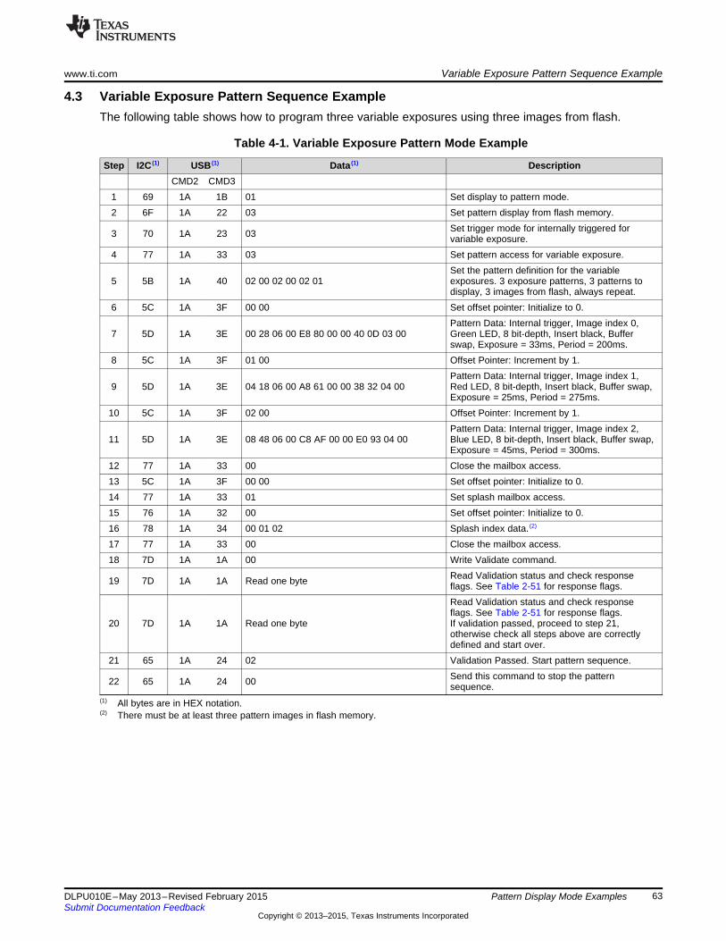
www.ti.com Variable Exposure Pattern Sequence Example
4.3 Variable Exposure Pattern Sequence ExampleThe following table shows how to program three variable exposures using three images from flash.
Table 4-1. Variable Exposure Pattern Mode Example
Step I2C (1) USB (1) Data (1) DescriptionCMD2 CMD3
1 69 1A 1B 01 Set display to pattern mode.2 6F 1A 22 03 Set pattern display from flash memory.
Set trigger mode for internally triggered for3 70 1A 23 03 variable exposure.4 77 1A 33 03 Set pattern access for variable exposure.
Set the pattern definition for the variable5 5B 1A 40 02 00 02 00 02 01 exposures. 3 exposure patterns, 3 patterns to
display, 3 images from flash, always repeat.6 5C 1A 3F 00 00 Set offset pointer: Initialize to 0.
Pattern Data: Internal trigger, Image index 0,7 5D 1A 3E 00 28 06 00 E8 80 00 00 40 0D 03 00 Green LED, 8 bit-depth, Insert black, Buffer
swap, Exposure = 33ms, Period = 200ms.8 5C 1A 3F 01 00 Offset Pointer: Increment by 1.
Pattern Data: Internal trigger, Image index 1,9 5D 1A 3E 04 18 06 00 A8 61 00 00 38 32 04 00 Red LED, 8 bit-depth, Insert black, Buffer swap,
Exposure = 25ms, Period = 275ms.10 5C 1A 3F 02 00 Offset Pointer: Increment by 1.
Pattern Data: Internal trigger, Image index 2,11 5D 1A 3E 08 48 06 00 C8 AF 00 00 E0 93 04 00 Blue LED, 8 bit-depth, Insert black, Buffer swap,
Exposure = 45ms, Period = 300ms.12 77 1A 33 00 Close the mailbox access.13 5C 1A 3F 00 00 Set offset pointer: Initialize to 0.14 77 1A 33 01 Set splash mailbox access.15 76 1A 32 00 Set offset pointer: Initialize to 0.16 78 1A 34 00 01 02 Splash index data. (2)
17 77 1A 33 00 Close the mailbox access.18 7D 1A 1A 00 Write Validate command.
Read Validation status and check response19 7D 1A 1A Read one byte flags. See Table 2-51 for response flags.Read Validation status and check responseflags. See Table 2-51 for response flags.
20 7D 1A 1A Read one byte If validation passed, proceed to step 21,otherwise check all steps above are correctlydefined and start over.
21 65 1A 24 02 Validation Passed. Start pattern sequence.Send this command to stop the pattern22 65 1A 24 00 sequence.
(1) All bytes are in HEX notation.(2) There must be at least three pattern images in flash memory.
63DLPU010E–May 2013–Revised February 2015 Pattern Display Mode ExamplesSubmit Documentation Feedback
Copyright © 2013–2015, Texas Instruments Incorporated

Variable Exposure Video Streaming Pattern Sequence Example www.ti.com
4.4 Variable Exposure Video Streaming Pattern Sequence ExampleThe following table shows how to program three variable exposures using images from video input.
Table 4-2. Variable Exposure Video Streaming Pattern Mode Example
Step I2C (1) USB (1) Data (1) DescriptionCMD2 CMD3
1 69 1A 1B 01 Set display to pattern mode.2 6F 1A 22 00 Set pattern display from video input source.
Set trigger mode for VSYNC triggered for3 70 1A 23 04 variable exposure.4 77 1A 33 03 Set pattern access for variable exposure.
Set the pattern definition for the variable5 5B 1A 40 02 00 02 00 00 01 exposures. 3 exposure patterns, 3 patterns to
display, always repeat.6 5C 1A 3F 00 00 Set offset pointer: Initialize to 0.
Pattern Data: External positive trigger, Image7 5D 1A 3E 01 28 06 00 10 27 00 00 E0 2E 00 00 index 0, Green LED, 8 bit-depth, Insert black,
Buffer swap, Exposure =10ms, Period = 12ms.8 5C 1A 3F 01 00 Offset Pointer: Increment by 1.
Pattern Data: External positive trigger, Image9 5D 1A 3E 04 18 06 00 28 23 00 00 10 27 00 00 index 1, Red LED, 8 bit-depth, Insert black,
Buffer swap, Exposure = 9ms, Period =10ms.10 5C 1A 3F 02 00 Offset Pointer: Increment by 1.
Pattern Data: External positive trigger, Image11 5D 1A 3E 09 48 06 00 F8 2A 00 00 B0 36 00 00 index 2, Blue LED, 8 bit-depth, Insert black,
Buffer swap, Exposure = 11ms, Period = 14ms.12 77 1A 33 00 Close the mailbox access.13 7D 1A 1A 00 Write Validate command. (2)
Read Validation status and check response14 7D 1A 1A Read one byte flags. See Table 2-51 for response flags.Read Validation status and check responseflags. See Table 2-51 for response flags.
15 7D 1A 1A Read one byte If validation passed, proceed to step 16,otherwise check all steps above are correctlydefined and start over.
16 65 1A 24 02 Validation Passed. Start pattern sequence.Send this command to stop the pattern17 65 1A 24 00 sequence.
(1) All bytes are in HEX notation.(2) A video source must be connect before performing this step.
64 Pattern Display Mode Examples DLPU010E–May 2013–Revised February 2015Submit Documentation Feedback
Copyright © 2013–2015, Texas Instruments Incorporated

www.ti.com Variable Exposure Video Streaming Pattern Sequence Example
65DLPU010E–May 2013–Revised February 2015 Pattern Display Mode ExamplesSubmit Documentation Feedback
Copyright © 2013–2015, Texas Instruments Incorporated

Appendix ADLPU010E–May 2013–Revised February 2015
Register Quick Reference
This appendix provides a quick reference summary of all available registers.
A.1 I2C Register Quick Reference
Table A-1. Register Quick Reference
I2C Address Description Type Reset Value Default Action0x00 Input Source Select WR 0x8 24-bit parallel interface0x02 Pixel Format WR 0x0 RGB 4:4:40x03 Port Clock Select WR 0x0 Port clock A0x04 Channel Swap WR 0x4 ABC = BAC0x05 FPD Mode WR 0x20 Pixel Mapping Mode 2 with
FPD-Link output mapped fromCONT1 onto Field Signal forFPD-Link interface port
0x06 Curtain Color Control WR 0x0 0x0 0x0 0x0 Curtain is black0x0 0x0
0x07 Power Control WR 0x0 Normal operation0x08 Long Axis Flip WR 0x0 Flip disabled0x09 Short Axis Flip WR 0x0 Flip disabled0x0A Test Pattern Select WR 0x8 RGB ramp0x0B LED PWM Polarity WR 0x0 Normal polarity0x10 LED Enable WR 0x8 LEDs controlled by Sequencer0x11 Get Version R 0x00010100 Version 1.1.00x13 Reset W 0x0 n/a0x1A Test Pattern Color WR 0x3FF 0x3FF White foreground, black
0x3FF 0x0 0x0 background0x0
0x20 Hardware Status R 0x1 No errors0x21 System Status R 0x1 No errors0x22 Main Status R 0x0 No errors0x26 CSC Data WR 0x400 0x0 0x0 RGB 4:4:4 Color-Space
0x0 0x400 0x0 Coefficients0x0 0x0 0x400
0x31 Gamma Control WR 0x8 Gamma Correction Enabled0x40 PWM Enable WR Channel Channel dependent
dependent0x41 PWM Setup WR Channel Channel dependent
dependent0x43 PWM Capture WR Channel Channel dependent
dependent0x44 GPIO Configuration WR Channel Channel dependent
dependent0x48 Clock Configuration WR Channel Channel dependent
dependent0x4B LED Current WR 0x97 0x78 0x7D LED PWMs
66 Register Quick Reference DLPU010E–May 2013–Revised February 2015Submit Documentation Feedback
Copyright © 2013–2015, Texas Instruments Incorporated

www.ti.com I2C Register Quick Reference
Table A-1. Register Quick Reference (continued)I2C Address Description Type Reset Value Default Action0x4E PWM Capture Read R Channel Channel dependent
Dependent0x61 Image Load Timing WR 0x0 n/a0x65 Pattern Start/Stop WR 0x0 Pattern stopped0x66 Pattern Exposure/Frame Rate Period WR 0x4010 0x411A 100-ms Exposure with 100-ms
frame rate0x69 Display Mode WR 0x0 Video Mode (Opposed to
Pattern Display Mode)0x6A Trigger Out 1 Control WR 0x0 0xBB 0xBB Normal Polarity with no rising or
falling delay0x6B Trigger Out 2 Control WR 0x0 0xBB Normal Polarity with no rising
delay0x6C Red Enable Delay WR 0xBB 0xBB No rising or falling delay0x6D Green Enable Delay WR 0xBB 0xBB No rising or falling delay0x6E Blue Enable Delay WR 0xBB 0xBB No rising or falling delay0x6F Pattern Display Mode WR 0x3 Display Patterns from flash0x70 Pattern Trigger Mode WR 0x1 Control Pattern Sequence with
internal or external trigger0x71 Buffer Swap WR 0x0 No Buffer Swap Performed0x72 Buffer Write Disable WR 0x0 Buffer Write Enabled0x73 Current Read Buffer WR 0x0 Current Buffer Streaming to
DMD is Buffer number 00x74 Invert Data WR 0x0 Normal operation0x75 Pattern Configuration WR 0x17 0x1 0x17 24 LUT Entries to be Repeated
0x0 in a Pattern Sequence of Length24, From 1 Flash Image
0x76 Mailbox Address W 0x0 No Offset to LUT Location0x77 Mailbox Control W 0x0 Malbox closed0x78 Mailbox Data W See Command See Command Description
Description0x79 Trigger In 1 Control WR 0x0 No delay0x7A Trigger In 2 Control WR 0x0 Advance Pattern Pair on Rising
Edge (for Trigger Mode 2)0x7C Buffer Freeze WR 0x1 Disable Buffer Swapping0x7D Validate R 0x0 Pattern Display Mode Settings
are valid0x7E Manual Input Display Resolution WR 0x0 0x0 0x0 0x0 Output Display Resolution is
0x0 0x0 0x500 1280 × 8000x320
0x7F Image Load WR 0xFF Last Image Index
Supported Commands in Firmware Version 2.0.0 or Greater0x5B Pattern Display Variable Exposure LUT WR 0x0 0x0 0x0 0x0 n/a
Control 0x0 0x00x5C Pattern Display Variable Exposure LUT WR 0x0 0x0 n/a
Offset Pointer0x5D Pattern Display Variable Exposure LUT W All 0x0 n/a
Data0x01 Input Video Signal Detection Status R 0x0 0x0 n/a0x62 Retrieve Image Resolution Information WR All 0x0 n/a
67DLPU010E–May 2013–Revised February 2015 Register Quick ReferenceSubmit Documentation Feedback
Copyright © 2013–2015, Texas Instruments Incorporated
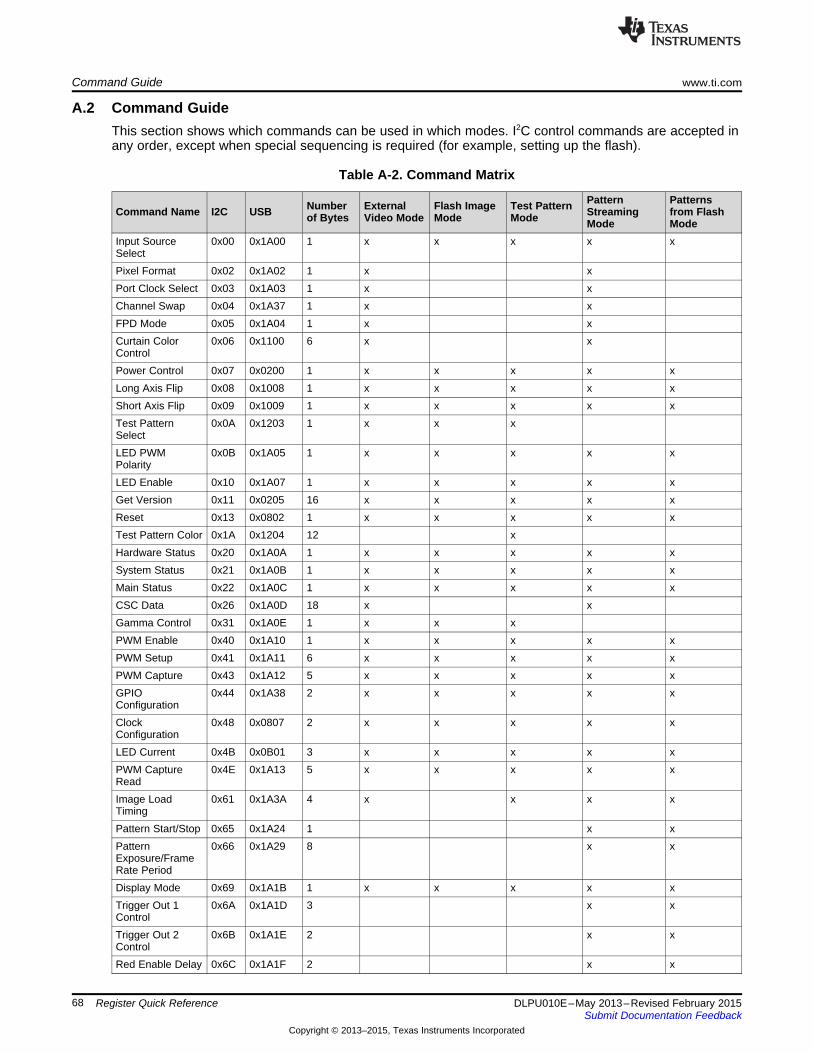
Command Guide www.ti.com
A.2 Command GuideThis section shows which commands can be used in which modes. I2C control commands are accepted inany order, except when special sequencing is required (for example, setting up the flash).
Table A-2. Command Matrix
Pattern PatternsNumber External Flash Image Test PatternCommand Name I2C USB Streaming from Flashof Bytes Video Mode Mode Mode Mode ModeInput Source 0x00 0x1A00 1 x x x x xSelectPixel Format 0x02 0x1A02 1 x xPort Clock Select 0x03 0x1A03 1 x xChannel Swap 0x04 0x1A37 1 x xFPD Mode 0x05 0x1A04 1 x xCurtain Color 0x06 0x1100 6 x xControlPower Control 0x07 0x0200 1 x x x x xLong Axis Flip 0x08 0x1008 1 x x x x xShort Axis Flip 0x09 0x1009 1 x x x x xTest Pattern 0x0A 0x1203 1 x x xSelectLED PWM 0x0B 0x1A05 1 x x x x xPolarityLED Enable 0x10 0x1A07 1 x x x x xGet Version 0x11 0x0205 16 x x x x xReset 0x13 0x0802 1 x x x x xTest Pattern Color 0x1A 0x1204 12 xHardware Status 0x20 0x1A0A 1 x x x x xSystem Status 0x21 0x1A0B 1 x x x x xMain Status 0x22 0x1A0C 1 x x x x xCSC Data 0x26 0x1A0D 18 x xGamma Control 0x31 0x1A0E 1 x x xPWM Enable 0x40 0x1A10 1 x x x x xPWM Setup 0x41 0x1A11 6 x x x x xPWM Capture 0x43 0x1A12 5 x x x x xGPIO 0x44 0x1A38 2 x x x x xConfigurationClock 0x48 0x0807 2 x x x x xConfigurationLED Current 0x4B 0x0B01 3 x x x x xPWM Capture 0x4E 0x1A13 5 x x x x xReadImage Load 0x61 0x1A3A 4 x x x xTimingPattern Start/Stop 0x65 0x1A24 1 x xPattern 0x66 0x1A29 8 x xExposure/FrameRate PeriodDisplay Mode 0x69 0x1A1B 1 x x x x xTrigger Out 1 0x6A 0x1A1D 3 x xControlTrigger Out 2 0x6B 0x1A1E 2 x xControlRed Enable Delay 0x6C 0x1A1F 2 x x
68 Register Quick Reference DLPU010E–May 2013–Revised February 2015Submit Documentation Feedback
Copyright © 2013–2015, Texas Instruments Incorporated

www.ti.com Command Guide
Table A-2. Command Matrix (continued)Pattern PatternsNumber External Flash Image Test PatternCommand Name I2C USB Streaming from Flashof Bytes Video Mode Mode Mode Mode Mode
Green Enable 0x6D 0x1A20 2 x xDelayBlue Enable 0x6E 0x1A21 2 x xDelayPattern Display 0x6F 0x1A22 1 x xModePattern Trigger 0x70 0x1A23 1 x xModeBuffer Swap 0x71 0x1A26 1 x x x x xBuffer Write 0x72 0x1A27 1 x x x x xDisableCurrent Read 0x73 0x1A28 1 x x x x xBufferInvert Data 0x74 0x1A30 1 x xPattern 0x75 0x1A31 4 x xConfigurationMailbox Address 0x76 0x1A32 1 x xMailbox Control 0x77 0x1A33 1 x xMailbox Data 0x78 0x1A34 4 x xTrigger In 1 0x79 0x1A35 4 x xControlTrigger In 2 0x7A 0x1A36 1 x xControlBuffer Freeze 0x7C 0x100A 1 x x x x xValidate 0x7D 0x1A1A 1 x xManual Input 0x7E 0x1000 16 xDisplayResolutionImage Load 0x7F 0x1A39 1 x x x x
Supported Commands in Firmware Version 2.0.0 or GreaterPattern Display 0x5D 0x1A3E 12 x xVariable ExposureLUT DataPattern Display 0x5C 0x1A3F 2 x xVariable ExposureLUT OffsetPointerPattern Display 0x5B 0x1A40 6 x xVariable ExposureLUT ControlInput Video Signal 0x01 0x071C 28 x xDetection StatusRetrieve Image 0x62 0x1A41 2 and (4 * x x x xResolution number ofInformation images)
69DLPU010E–May 2013–Revised February 2015 Register Quick ReferenceSubmit Documentation Feedback
Copyright © 2013–2015, Texas Instruments Incorporated

Command Guide www.ti.com
70 Register Quick Reference DLPU010E–May 2013–Revised February 2015Submit Documentation Feedback
Copyright © 2013–2015, Texas Instruments Incorporated
www.ti.com Revision E History
Revision E History
Changes from D Revision (July 2014) to E Revision ...................................................................................................... Page
• Changed Clock Period bytes from 3:1 to 4:1 and Duty Cycle from byte 4 to 5.................................................. 34
Revision D History
Changes from C Revision (April 2014) to D Revision .................................................................................................... Page
• Corrected upper frequency limit of I2C communication .............................................................................. 7• Added emphasis to sentences about read and write bytes for DLPC350 sub-address ......................................... 7• Corrected I2C read register and graphic to show only one byte.................................................................... 8• Updated I2C Write Sequence and figure with 1 byte sub-address ................................................................. 9• Added a note on accessing undocumented registers............................................................................... 12• Added note to correct errors from Hardware Status Register ..................................................................... 13• Added reset for byte 3:0 for Get Version Command ................................................................................ 14• Added 24-bit frame buffers to example for Buffer Write Disable command...................................................... 20• Corrected formatting of FPD-Link Mode and Field Select Command table...................................................... 22• Added Parallel Port to Port Clock Select heading ................................................................................... 23• Adjusted Input Pixel Data Format Command formatting ........................................................................... 24• Added a Note about changing an image flip settings ............................................................................... 27• Provided an upper limit for frequency of pattern display sequences.............................................................. 35• Added note for changing Pattern Display............................................................................................. 40• Added note for using Validate Data Command after Pattern Display changes ................................................. 40• Corrected table title: Validate Data Command Response.......................................................................... 41• Added bit 7 info for validate data command table ................................................................................... 41• Added note about reading response byte of Validate Data Command ........................................................... 41• Added clarification of when Trigger modes apply for Mode 0, 1, and 2 .......................................................... 41• Added new trigger modes for variable exposure in 2.4.3.2.1. ..................................................................... 43• Added two clarifications about delay control range to Trigger Out1 and Trigger Out2 tables ................................. 44• Added clarifications about delay control range to Red, Green, and Blue LED Enable Control tables ....................... 46• Added a note about stopping and starting Pattern Display Sequence ........................................................... 48• Moved example of Frame Period into a Note. ....................................................................................... 48• Added new mailbox for variable exposure in 2.4.3.4.8.............................................................................. 50• Added emphasis to Pattern Display LUT Data information ........................................................................ 51• Added new variable exposure command in 2.4.3.4.10. ............................................................................ 53• Added new variable exposure command in 2.4.3.4.11. ............................................................................ 54• Added new variable exposure command in 2.4.3.4.12. ............................................................................ 54• Added flowchart example for programming a variable exposure pattern sequence. ........................................... 56• Added variable exposure pattern sequence example in 4.3. ...................................................................... 63• Added variable exposure video streaming pattern sequence example in 4.4. .................................................. 64• Added new commands to Appendix A for firmware version 2.0.0................................................................. 66• Added I2C command clarification to Appendix A2 .................................................................................. 68• Added new commands to Appendix A2 for firmware version 2.0.0. .............................................................. 68
Revision C History
Changes from B Revision (August 2013) to C Revision ................................................................................................ Page
• Corrected DLPC350 slave address when I2C_ADDR_SEL pin is high ............................................................ 7• Changed typographical error that stated I2C write bit is active high ............................................................... 7
71DLPU010E–May 2013–Revised February 2015 Revision HistorySubmit Documentation Feedback
Copyright © 2013–2015, Texas Instruments Incorporated

Revision B History www.ti.com
• Added information about DLPC350 sub-address read/write bit that was not present in Rev B ................................ 7• Updated sub-address of write example sequence.................................................................................... 8• Updated I2C Write Sequence figure with correct sub-address...................................................................... 9• Added clarification for Programming Commands section differentiating between program mode and normal mode of
DLPC350 operation...................................................................................................................... 15• Changed Return Checksum command to correct Read Control command...................................................... 18• Corrected bit position for GPIO Clock Configuration command to bit 0 and 1 .................................................. 33• Fixed typo in PWM Control command ................................................................................................ 33• Added a step to disable GPIO pins before enabling PWM functionality.......................................................... 33• Display Mode Selection bit was reversed between Video mode and Pattern Display mode .................................. 39• Included a calculation of Pattern Exposure time and Frame Period .............................................................. 48
Revision B History
Changes from A Revision (July 2013) to B Revision ..................................................................................................... Page
• Changed Current Control Unit From 1/2 256 Steps to 256 Steps................................................................. 31• Changed Trigger Signals to follow TRIG_X_X Format ............................................................................. 41• Changed Description of Pattern Exposure and Frame Period..................................................................... 49• Changed Description of Number of Patterns in LUT Control Command ......................................................... 50• Changed Black-Fill Time from 225 µs to 230 µs .................................................................................... 52
Revision A History
Changes from Original (May 2013) to A Revision ........................................................................................................... Page
• Added Input Value Bits for GPIO Configuration ..................................................................................... 32• Added GPIO Channel Byte for PWM Capture ....................................................................................... 35• Changed Max TRIG_OUT_1 Delays .................................................................................................. 44• Changed Pattern Exposure and Frame Period Values ............................................................................. 49• Changed Default Number of Patterns in LUT ........................................................................................ 50• Changed Default Pattern LUT.......................................................................................................... 52• Deleted Temperature Commands from Register Quick Reference ............................................................... 66• Deleted Temperature Commands from Command Matrix ......................................................................... 68
72 Revision History DLPU010E–May 2013–Revised February 2015Submit Documentation Feedback
Copyright © 2013–2015, Texas Instruments Incorporated

IMPORTANT NOTICE
Texas Instruments Incorporated and its subsidiaries (TI) reserve the right to make corrections, enhancements, improvements and otherchanges to its semiconductor products and services per JESD46, latest issue, and to discontinue any product or service per JESD48, latestissue. Buyers should obtain the latest relevant information before placing orders and should verify that such information is current andcomplete. All semiconductor products (also referred to herein as “components”) are sold subject to TI’s terms and conditions of salesupplied at the time of order acknowledgment.TI warrants performance of its components to the specifications applicable at the time of sale, in accordance with the warranty in TI’s termsand conditions of sale of semiconductor products. Testing and other quality control techniques are used to the extent TI deems necessaryto support this warranty. Except where mandated by applicable law, testing of all parameters of each component is not necessarilyperformed.TI assumes no liability for applications assistance or the design of Buyers’ products. Buyers are responsible for their products andapplications using TI components. To minimize the risks associated with Buyers’ products and applications, Buyers should provideadequate design and operating safeguards.TI does not warrant or represent that any license, either express or implied, is granted under any patent right, copyright, mask work right, orother intellectual property right relating to any combination, machine, or process in which TI components or services are used. Informationpublished by TI regarding third-party products or services does not constitute a license to use such products or services or a warranty orendorsement thereof. Use of such information may require a license from a third party under the patents or other intellectual property of thethird party, or a license from TI under the patents or other intellectual property of TI.Reproduction of significant portions of TI information in TI data books or data sheets is permissible only if reproduction is without alterationand is accompanied by all associated warranties, conditions, limitations, and notices. TI is not responsible or liable for such altereddocumentation. Information of third parties may be subject to additional restrictions.Resale of TI components or services with statements different from or beyond the parameters stated by TI for that component or servicevoids all express and any implied warranties for the associated TI component or service and is an unfair and deceptive business practice.TI is not responsible or liable for any such statements.Buyer acknowledges and agrees that it is solely responsible for compliance with all legal, regulatory and safety-related requirementsconcerning its products, and any use of TI components in its applications, notwithstanding any applications-related information or supportthat may be provided by TI. Buyer represents and agrees that it has all the necessary expertise to create and implement safeguards whichanticipate dangerous consequences of failures, monitor failures and their consequences, lessen the likelihood of failures that might causeharm and take appropriate remedial actions. Buyer will fully indemnify TI and its representatives against any damages arising out of the useof any TI components in safety-critical applications.In some cases, TI components may be promoted specifically to facilitate safety-related applications. With such components, TI’s goal is tohelp enable customers to design and create their own end-product solutions that meet applicable functional safety standards andrequirements. Nonetheless, such components are subject to these terms.No TI components are authorized for use in FDA Class III (or similar life-critical medical equipment) unless authorized officers of the partieshave executed a special agreement specifically governing such use.Only those TI components which TI has specifically designated as military grade or “enhanced plastic” are designed and intended for use inmilitary/aerospace applications or environments. Buyer acknowledges and agrees that any military or aerospace use of TI componentswhich have not been so designated is solely at the Buyer's risk, and that Buyer is solely responsible for compliance with all legal andregulatory requirements in connection with such use.TI has specifically designated certain components as meeting ISO/TS16949 requirements, mainly for automotive use. In any case of use ofnon-designated products, TI will not be responsible for any failure to meet ISO/TS16949.
Products ApplicationsAudio www.ti.com/audio Automotive and Transportation www.ti.com/automotiveAmplifiers amplifier.ti.com Communications and Telecom www.ti.com/communicationsData Converters dataconverter.ti.com Computers and Peripherals www.ti.com/computersDLP® Products www.dlp.com Consumer Electronics www.ti.com/consumer-appsDSP dsp.ti.com Energy and Lighting www.ti.com/energyClocks and Timers www.ti.com/clocks Industrial www.ti.com/industrialInterface interface.ti.com Medical www.ti.com/medicalLogic logic.ti.com Security www.ti.com/securityPower Mgmt power.ti.com Space, Avionics and Defense www.ti.com/space-avionics-defenseMicrocontrollers microcontroller.ti.com Video and Imaging www.ti.com/videoRFID www.ti-rfid.comOMAP Applications Processors www.ti.com/omap TI E2E Community e2e.ti.comWireless Connectivity www.ti.com/wirelessconnectivity
Mailing Address: Texas Instruments, Post Office Box 655303, Dallas, Texas 75265Copyright © 2015, Texas Instruments Incorporated