dissertation engineering of aerosol-jet printed carbon
TRANSCRIPT

Dissertation
zur
Erlangung der Doktorwürde (Dr. rer. nat.)
der
Naturwissenschaftlich-Mathematischen Gesamtfakultät
der
Ruprecht-Karls-Universität Heidelberg
Thema
Engineering of Aerosol-Jet Printed
Carbon Nanotube Network Transistors
Vorgelegt von
Marcel Rother
geboren in Meißen
Gutachter
Prof. Dr. Jana Zaumseil
Prof. Dr. Uli Lemmer
Tag der mündlichen Prüfung: 08. März 2019


Dissertation
to obtain the degree of
Doctor of the Natural Sciences (Dr. rer. nat.)
submitted to the
Combined Faculty of Natural Sciences and Mathematics
at
Heidelberg University, Germany
Topic
Engineering of Aerosol-Jet Printed
Carbon Nanotube Network Transistors
Presented by
Marcel Rother (M. Sc.)
born in Meißen
Reviewer
Prof. Dr. Jana Zaumseil
Prof. Dr. Uli Lemmer
Oral examination: March 08th, 2019


I
If you thought science was certain – well, that is just an error on your part.
Richard P. Feynman

II

III
ACKNOWLEDGEMENTS
This thesis and the experimental work behind it would not have been possible without the help,
support, guidance, and cooperation of a vast number of friends, colleagues, partners, and family.
First of all, I want to thank Jana Zaumseil not only for enabling to work on the scientific projects
included in this work and the associated academic advice, constructive criticism, and guidance,
but also for the possibility to accompany several non-academic projects and develop the
workflows in this group, the thereby trusted confidence in my work, and the expressed
appreciation.
During the years in the Nanomaterials for Optoelectronics (NMOE) group I had the pleasure to
share offices (in 2 cities and 3 buildings) with Florentina Gannott, Stefan Schießl, Manuel
Schweiger, Stefan Grimm, Maximilian Brohmann, Maik Matthiesen, Kevin Synnatschke,
and Felix Berger, who made late work and long days more bearable and beyond that became
good friends that helped in various situations and ensured enjoyable after-work activities.
A lot more full-time group members supported me, became friends, and/or were involved in
activities in and out of the lab, namely Martin Held, Severin Schneider, Florian Jakubka, Julia
Binder, Yuriy Zakharko, Katrin Ludwig, Arko Graf, Claudia Backes, Farnia Rashvand,
Chloe Francis, Fabian Paulus, Katelyn Goetz, Thomas Higgins, Vaishnavi Rao, Jan
Lüttgens, Sebastian Grieger, Maximilian Krings, Steffen Ott, and Merve Balci.
There have been several students under my supervision that evaluated new materials, tested
parameters, optimized processes and thereby contributed to this work whether visibly or invisibly:
Andreas Malhofer, Shuyi Yang, Steffen Ott, Caroline Krzyszkowski, Adelaide Kruse, and
Marian Rosenthal.
At the chair for Applied Physical Chemistry, quite a few people organized or assisted with
administrative issues: Karin Jordan, Svetlana Duchnay, Benjamin Scherke, Rainer Dahint,
Michael Zharnikov, and Matthias Jankowski.
A lot of experiments or setups for fabrication and evaluation would not have been possible without
the technical stuff of the mechanics workshop, Klaus Schmitt, Marco Billmaier, Mert Kaya,
Andreas Kreiter, Jonas Windelband, or IT and technical support from Peter Jeschka, Günter
Meinusch, and Reinhold Jehle.

IV
Right at the beginning of my work for this thesis, I had the opportunity to stay at the University
of Minnesota and get first-hand experience on the aerosol-jet printer that would accompany me
for more than 3 years thereafter. Thanks to Daniel Frisbie and Scott White for hosting and
supporting me, as well as Dayne Plemmons, Boo Schliep and all the others I met during the time
who made it very enjoyable and informative.
In Heidelberg also a lot more supporters need to be mentioned as they helped with advice, support,
and information of all kinds: Silke Koser from the Institute for Organic Chemistry, Stefan
Kauschke, Olaf Skibbe, and Martina Anselmann from the Center of Advanced Materials,
Thomas Peissig, Karsten Bensch, Kai Sudau, Martin Gutfleisch, Gerardo Hernández-Sosa,
Sebastian Stolz, Tobias Rödlmeier, Hildegard Merkle, and Anne-Katherine Mang from the
InnovationLab GmbH, Alexey Tarasov, Marcin Filipiak, and Natalie Haustein from BioMedX
GmbH.
A special thanks to all the proofreaders that helped to free this thesis of typos and other errors.
Many of those I spent time with working and learning in the last decade became and stayed very
good friends. I especially want to thank those that made it possible to stay in contact even after
scattering all about Germany and its neighboring countries. Every time we manage to meet despite
the distances and full calendars, it feels like we met the last time just a week before. Thanks to all
my friends for mental, emotional, and practical support, for the fun times we had and will have in
the future. Thanks to the ones I became friends with through school or handball while still living
in Kleinwallstadt. Thanks to my friends from Würzburg, Toronto, and Erlangen. We spent a
lot of time together during the studies and had a great time together. Thanks to everyone I met in
Heidelberg and I am still happy to meet anytime soon again, although some of you already moved
and now I followed this trend and left Heidelberg after some time. Unfortunately, I cannot name
all of you in person or this document would get even much longer.
Ein besonderer Dank geht an meine Familie, vor allem an meine Eltern für die Unterstützung
vor, während und nach dem Studium, für viele liebgemeinte und ernste Ratschläge, für die Zeit
die Ihr für mich aufgewendet habt, und dafür, dass ihr immer für mich da seid, sowie meine
Großeltern für die jahrelange Unterstützung.
Last but not least I want to thank Fiona for being with me, being there for me, supporting me,
enduring my flaws, and pushing me to finishing up this work.

V
ABSTRACT
Thanks to their extremely high mobilities, semiconducting carbon nanotubes (CNTs) are a
promising material for high speed electronics. Beyond that, CNT networks are inherently flexible
and stretchable and can be processed from dispersions resulting in devices with still remarkable
electronic properties. They can fulfill many of the various requirements for novel applications
including fast switching speeds and high currents at low drive voltages. Depending on the
intended use, one or another device property might be more important. CNT networks, processes,
and architectures can be tailored to yield devices that can serve the respective purpose. Highly
purified semiconducting CNTs are, however, still rather expensive and direct-write techniques are
thus preferred to enable variable designs and reduce manufacturing costs.
In this work, aerosol-jet printing is investigated as a deposition technique for CNTs that works
with small ink volumes but can also be upscaled by parallelization and integrated into high-
throughput roll-to-roll printing processes. After the development of printable inks, it is shown that
the printing process itself has no influence on the quality of the CNTs although sonication is used
to transfer the ink into an aerosol. The electronic properties of CNT networks incorporated in an
established transistor structure exhibit reproducibility comparable to other deposition techniques.
Moreover, additive manufacturing enables the deposition of several layers on top of each other to
increase the overall film thickness up to optically dense films visible to the naked eye. Field-effect
mobilities and on-conductances increase and the hysteresis decreases for thicker films compared
to dense but thin networks.
Based on these findings, CNT films are printed with a thickness of 50–600 nm and vertical charge
transport is demonstrated. These films are subsequently sandwiched between electrodes and
electrolyte-gating results in doping of CNT films throughout electrode overlap areas of several
hundred µm2. The vertical device architecture decouples the printing accuracy from the critical
device dimensions while supporting high currents for a small footprint. A comparison of different
printed electrode materials reveals the superior properties of printed metals over mixed (metallic
and semiconducting) CNTs. Electrodes based on inkjet-printed gold nanoparticles are additionally
used on flexible substrates and stable device performance even after several hundred bending
cycles is demonstrated for vertical and lateral CNT network transistors. These all-printed devices
are promising for further development of electronic circuits that do not require high operating
frequencies but rather flexibility, high-currents, and small footprints.

VI

VII
KURZFASSUNG
Dank ihrer extrem hohen Ladungsträgermobilität sind halbleitende Kohlenstoff-Nanoröhrchen
(engl. carbon nanotubes, CNTs) ein vielversprechendes Material für Anwendungen in der
Hochgeschwindigkeitselektronik. Darüber hinaus sind Netzwerke aus CNTs flexibel, dehnbar und
können aus Dispersionen abgeschieden werden. Transistoren basierend auf CNT-Netzwerken
weisen noch immer bemerkenswerte elektronische Eigenschaften auf. Sie sind daher für diverse
neue Anwendungen geeignet, welche nicht nur hohe Schaltgeschwindigkeiten und Ströme – bei
gleichzeitig niedrigen Spannungen – benötigen. Je nach gewünschter Anwendung ist hierbei die
eine oder andere Eigenschaft maßgebend. CNT-Netzwerke, Prozesse und Bauteil-Architekturen
können entsprechend angepasst werden, um Transistoren zu fertigen, welche die jeweiligen
Anforderungen optimal erfüllen. Da das aufgereinigte Material jedoch noch immer relativ teuer
ist, wird die Abscheidung mittels direkt strukturierender Prozesse bevorzugt, um variable Designs
zu ermöglichen und die Herstellungskosten zu senken.
In dieser Arbeit wird das Aerosol-Jet-Drucken als eine Möglichkeit zur Abscheidung betrachtet,
welche auch mit kleinen Tintenvolumina arbeiten und gleichzeitig durch Parallelisierung
hochskaliert und in Rolle-zu-Rolle-Prozesse mit hohem Durchsatz integriert werden kann.
Zunächst werden druckbare Tinten entwickelt, bevor gezeigt wird, dass der Druckprozess selbst
keinen Einfluss auf die Qualität der CNTs hat, obwohl Ultraschall zur Aerosol-Bildung eingesetzt
wird. Die Reproduzierbarkeit der Transistoreigenschaften, welche in einem ähnlichen Bereich wie
jene anderer Abscheidungstechniken liegt, wird mittels einer etablierten Transistor-Architektur,
in welche die gedruckten CNT-Netzwerke eingebaut werden, untersucht. Durch das Drucken von
mehreren Schichten übereinander ist es weiterhin möglich, dicke Filme zu erhalten, welche mit
bloßem Auge sichtbar sind. Verglichen mit dichten aber dünnen Netzwerken, weisen Transistoren
mit dickeren Filmen höhere Feld-Effekt-Mobilitäten und Ströme bei gleichzeitig niedrigerer
Hysterese auf.
Anhand von Schichten mit einer Dicke von 50–600 nm wird anschließend der Ladungstransport
in vertikaler Richtung durch den CNT-Film demonstriert. Der Ladungstransport durch Filme,
welche zwischen Goldelektroden eingebettet sind, kann mittels einer an einer dritten Elektrode
angelegten Spannung und eines Elektrolyten als Dielektrikum, selbst bei einem Überlapp der
Elektroden von mehreren hundert Quadratmikrometern, ein- und ausgeschaltet werden. Diese
vertikale Transistor-Architektur entkoppelt die kritischen Transistor-Dimensionen von der

VIII
Genauigkeit des Druckprozesses, während hohe Ströme bei einer kleinen Grundfläche realisierbar
sind. Ein Vergleich verschiedener gedruckter Elektrodenmaterialien zeigt sich die Überlegenheit
von metallischen Materialien gegenüber gemischten (metallischen und halbleitenden) CNT-
Netzwerken. Mittels Inkjet-gedruckten Elektroden aus Gold-Nanopartikeln kann ein stabiles
Transistor-Verhalten auch nach mehreren hundert Biegezyklen auf flexiblen Substraten gezeigt
werden. Diese vollständig gedruckten Transistoren sind vielversprechend für die weitere
Entwicklung von elektronischen Schaltkreisen, welche mechanische Flexibilität und hohe Ströme
bei niedrigem Flächenbedarf anstelle hoher Schaltfrequenzen benötigen.

IX
CONTENTS
ACKNOWLEDGEMENTS III
ABSTRACT V
KURZFASSUNG VII
1. INTRODUCTION 1
2. BACKGROUND 5
2.1. Carbon Nanotubes ................................................................................................. 6
2.1.1. Overview .......................................................................................................... 6
2.1.2. Band structure ................................................................................................... 7
2.1.3. CNT Chirality determination .......................................................................... 11
2.1.4. Electronic properties ....................................................................................... 15
2.1.5. Synthesis ......................................................................................................... 16
2.1.6. Chirality separation ........................................................................................ 17
2.2. Carbon Nanotube Transistors .............................................................................. 19
2.2.1. Overview ........................................................................................................ 19
2.2.2. Device architectures ....................................................................................... 20
2.2.3. Layer Deposition and Structuring .................................................................. 21
2.2.4. Unipolar Thin-Film Field-Effect Transistors – Basic Principles ................... 22
2.2.5. Extraction of Device Parameters .................................................................... 25
2.2.6. Ambipolar Field-Effect Transistors ................................................................ 28
2.2.7. Networks and Arrays of CNTs as Thin-Film Semiconductors ...................... 30
2.2.8. Electrolyte-Gated Transistors ......................................................................... 32
2.3. Printed Electronics .............................................................................................. 36
2.3.1. Overview ........................................................................................................ 36
2.3.2. Materials for Printed Transistors .................................................................... 37
2.3.3. Printing methods ............................................................................................. 39
2.4. Aerosol-Jet Printing ............................................................................................ 44

Contents
X
2.4.1. Working principle ...........................................................................................44
2.4.2. (Partially) Aerosol-Jet Printed Devices ..........................................................46
3. EXPERIMENTAL 49
3.1. Alterations to the Optomec Aerosol-Jet System ..................................................50
3.2. Device Fabrication ...............................................................................................52
3.2.1. Carbon Nanotube Dispersions ........................................................................52
3.2.2. Electrode Patterning ........................................................................................53
3.2.3. Aerosol-Jet Printing of CNTs .........................................................................55
3.2.4. Airbrush Spraying of TUBALL Nanotubes ....................................................57
3.2.5. Fabrication of Transistors ...............................................................................57
3.3. Characterization ...................................................................................................58
3.3.1. Absorption Spectroscopy ................................................................................58
3.3.2. Profilometry ....................................................................................................58
3.3.3. (Conductive) Atomic Force Microscopy ........................................................58
3.3.4. Scanning Electron Microscopy .......................................................................58
3.3.5. Raman Spectroscopy .......................................................................................59
3.3.6. Electrical Characterization ..............................................................................59
4. MATERIALS AND DEVICES 61
4.1. Materials ..............................................................................................................62
4.2. Devices ................................................................................................................66
5. AEROSOL-JET PRINTING OF CARBON NANOTUBES 71
5.1. Introduction .........................................................................................................72
5.2. Ink Formulation ...................................................................................................73
5.3. Stability of Carbon Nanotube Inks ......................................................................79
5.4. Reproducibility of Transistor Characteristics ......................................................87
5.5. Decreasing the Hysteresis of Aerosol-Jet-Printed CNTs ....................................96
5.6. Applications of Printed CNT Films ...................................................................102
5.7. Limitations of Aerosol-Jet Printing for CNTs ...................................................103
6. VERTICAL ELECTROLYTE-GATED TRANSISTORS 105
6.1. Introduction .......................................................................................................106
6.2. Three-Dimensional Charge Transport and Efficient Gating .............................108
6.3. Device Characteristics of VEGTs ......................................................................113
Contents
XI
6.4. Lateral Charge Transport Pathways .................................................................. 122
6.5. Comparison to Lateral Transistors .................................................................... 125
6.6. All-Printed VEGTs............................................................................................ 127
6.6.1. Airbrush-sprayed Mixed Carbon Nanotube Electrodes ............................... 128
6.6.2. Aerosol-jet Printed Silver Nanoparticle Electrodes ..................................... 130
6.6.3. Inkjet-printed Gold Nanoparticle Electrodes................................................ 132
6.6.4. Comparison of the Different Electrode Materials ........................................ 135
7. FLEXIBLE TRANSISTORS 139
7.1. Introduction ....................................................................................................... 140
7.2. Vertical and Lateral CNT Transistors Directly Printed on Plastic Substrates .. 140
7.3. Bending Vertical and Lateral EGTs .................................................................. 145
8. CONCLUSIONS AND OUTLOOK 151
BIBLIOGRAPHY 157
APPENDIX 201
A. List of Frequently Used Abbreviations ............................................................. 201
B. List of Frequently Used Symbols ...................................................................... 203
C. List of Figures ................................................................................................... 205
D. List of Tables ..................................................................................................... 213
E. Publications ....................................................................................................... 215

XII

1
CHAPTER 1
1.INTRODUCTION

Introduction
2
For more than 70 years transistors have been the fundamental components of virtually all modern
electronic products and ensure the operation of a wide range of electronic devices from simple
circuits, sensors, and controllers, to telecommunication and data processing in combination with
computers and mobile phones. Over the last decades, the improvement of transistors and their
applications has been mostly driven by cost reduction and miniaturization.
More recently, the restrictions of traditional rigid silicon and other inorganic semiconductors were
sought to be overcome to achieve freedom of design and shape as well as overall flexibility of the
final products. Existing prototypes, design drafts, and already available products include rollable
or foldable displays, light-sources, and solar cells, stretchable sensors, intelligent clothing, and
more. The realization of unlimited flexibility and stretchability, requires new materials and/or
device architectures that are compatible with mechanical deformation.
Moving towards flexible devices simultaneously introduces the necessity to develop new
fabrication methods. Batch production – often requiring vacuum and/or high temperature
processing – is traditionally used in silicon electronics with areal material deposition that requires
subsequent high-resolution patterning (top-down). Flexible substrates on the other hand enable
roll-to-roll processing technologies known from newspaper printing with direct and additive
patterning of the deposited material (bottom-up). Printing technologies could reduce the
manufacturing costs of electronic devices, due to high throughput, fast and simple variation of the
printing patterns and low processing temperatures. However, the achievable resolution and
registration are limited.
Networks of single-walled carbon nanotubes (CNTs) are one of the promising material candidates
for printed electronics on flexible or stretchable substrates. While a mixture of ⅓ metallic and ⅔
semiconducting nanotubes is produced during synthesis, recent advances in sorting techniques
enable the dispersion of almost purely semiconducting species.[1] Printed nanotube networks can
thus not only be used as electrodes but also as the semiconductor in light-emitting diodes,
photovoltaics, and transistors. Although nanotube networks cannot reach the charge carrier
mobilities of individual CNTs (up to several thousand cm2 V−1 s–1) due to limitations by
nanotube–nanotube junctions, current CNT network field-effect transistors were able to achieve
charge carrier mobilities of more than 100 cm2 V−1 s–1.[2] Utilized as conductors, sheet resistances
of less than 100 Ω −1 were reported even for semi-transparent CNT layers.[3, 4]

Introduction
3
Besides their favorable mechanical and electronic properties, CNTs can be readily dispersed in
organic solvents or water, which makes them ideal candidates for printing processes at low
temperatures.[1] Although various printed electronic devices have been demonstrated, it remains
to be evaluated, which deposition method is most suitable for the different layers of a transistor.
Depending on the application, transistors based on printed CNTs have to fulfill a number of
requirements, e.g. reproducibility, high on/off-ratios, fast switching speeds, long-term stability,
high current densities, small footprint, flexibility, and stretchability. Moreover, compared to
photolithographic structuring methods, the achievable resolution and layer-to-layer registration is
lower by several orders of magnitude. Hence, the printing parameters have to be carefully
optimized and device architectures have to be adapted or specifically developed.
Especially for transistors with variable designs, prototypes, or proof-of-concept studies, direct-
write technologies that do not waste a large amount of material and can work with small ink
volumes are desired, as purified nanotube material containing almost only semiconducting CNTs
is still rather precious. The inks should also be free of additives as far as possible to avoid any
negative impact on the charge transport through the deposited networks. These requirements are
fulfilled by aerosol-jet printing,[5] a relatively new printing method that is used in this work for
the deposition of networks of semiconducting (6,5) CNTs. After analyzing the reproducibility of
device performance in a conventional transistor architecture, this technique was also used to
deposit rather thick films for vertical charge transport in all-printed devices that overcome
resolution limitations. Finally, lateral and vertical devices were fabricated on flexible polymer
substrates and evaluated with respect to bending.
Chapter 2 gives an overview about carbon nanotubes including their band structure, electronic
properties, and synthesis methods. Furthermore, methods to separate metallic and semiconducting
CNTs and to determine the chirality of a CNT are introduced. The theoretical framework to
understand unipolar and ambipolar transistors is provided and device architectures and patterning
processes are explained. After an overview of materials and techniques used for printed
electronics and the previously demonstrated devices, aerosol-jet printing as the main method used
and evaluated in this work is presented.
Chapter 3 details the experimental procedures employed for device fabrication and
characterization followed by the exact descriptions of materials and devices in chapter 4.

Introduction
4
The results of the experimental work are presented in the subsequent sections. Chapter 5 starts
with the formulation of carbon nanotube inks suitable for aerosol-jet printing of the
semiconducting layer in transistors. After evaluating the stability of these inks, the reproducibility
of transistors printed from this material is examined with an established device structure. The
initially rather high hysteresis is decreased by different techniques and applications of the printed
CNT films, e.g. in electrochromic devices and transistors for different studies, based on the
findings made before, are presented. This section ends with the description of limitations
encountered during the preparation of CNT films via aerosol-jet printing.
While the focus of chapter 5 was mainly on the semiconducting nanotube network and thus
photolithographically structured electrodes were used, chapter 6 utilizes a recently developed
vertical device architecture to avoid device dimensions that are incompatible with printing
resolution and alignment accuracy. The necessary demonstration of three-dimensional charge
transport and efficient electrolyte-gating of the whole nanotube network is followed by the
resulting device characteristics and the comparison with lateral transistors fabricated from the
same materials. Different electrode materials are subsequently evaluated with regard to the final
device performance.
In Chapter 7 the established procedures for lateral and vertical transistors based on aerosol-jet
printed semiconducting CNTs are utilized to fabricate bendable devices on plastic substrates.
Chapter 8 summarizes the insights gained in this thesis and gives suggestions for future
experiments and potential applications.

5
CHAPTER 2
2.BACKGROUND
This chapter provides the theoretical background on carbon
nanotubes and transistors followed by an overview about
methods and materials for printed electronics including
aerosol-jet printing.

Background
6
2.1. Carbon Nanotubes
2.1.1. Overview
For a long time, only amorphous carbon and two ordered carbon modifications have been known
– diamond and graphite. Both modifications are well-studied and exhibit unique properties:
Diamond is the hardest naturally occurring material and graphite shows – due to its planar crystal
structure – strong anisotropy in its physical properties.[6] The discovery of new nano-scale carbon
modifications started in 1985 with zero-dimensional fullerenes,[7] followed by one-dimensional
carbon nanotubes (CNTs) which were first synthesized in 1991.[8] The two-dimensional graphene,
essentially a single layer of graphite, was eventually found in 2004 and completed the range of
low-dimensional carbon allotropes.[9] Further modifications of these structures were synthesized
later, e.g. graphene nanoribbons (laterally confined graphene),[10, 11] carbon nano-onions (multi-
walled fullerenes),[12, 13] or carbon nano-horns.[14] While multi-walled carbon nanotubes were
synthesized and investigated as well, single-walled CNTs are particularly interesting because of
their unique electronic properties. In this work, only single-walled CNTs were used and thus the
term carbon nanotube refers to them only in this context.
Defect-free graphene consists of sp2-hybridized carbon atoms arranged in hexagons within a two-
dimensional plane. CNTs can be described as rolled-up graphene sheets forming one-dimensional
hollow tubes. Depending on the direction and circumference of this rolled-up graphene sheet,
different nanotubes are possible. The (n,m) notation commonly used to distinguish different CNT
chiralities describes the vector along the nanotube circumference which is derived from the linear
combination of the unit vectors a1 and a2 of the graphene unit cell, where a = 0.246 nm is the
lattice constant (compare Figure 2.1):[1]
= ∙ + ∙ = ∙ 2 ∙ √3, 1 + ∙ 2 ∙ √3,−1 (2.1)
The alternative description of a CNT with the nanotube diameter d and the chiral angle Θ can be
directly derived from this vector c. Note that the chiral angle is defined as the angle between the
chiral vector and the chiral vector of a zigzag nanotube, i.e. a nanotube with m = 0.
= || = ∙ √ + 2 ∙ ∙ + (2.2)
= arctan √3 ∙ 2 ∙ + (2.3)
Background
7
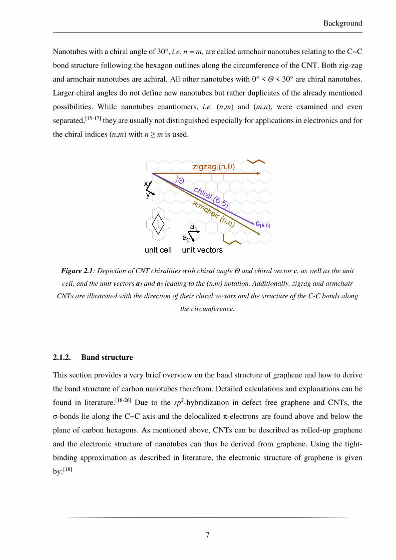
Nanotubes with a chiral angle of 30°, i.e. n = m, are called armchair nanotubes relating to the C−C
bond structure following the hexagon outlines along the circumference of the CNT. Both zig-zag
and armchair nanotubes are achiral. All other nanotubes with 0° < Θ < 30° are chiral nanotubes.
Larger chiral angles do not define new nanotubes but rather duplicates of the already mentioned
possibilities. While nanotubes enantiomers, i.e. (n,m) and (m,n), were examined and even
separated,[15-17] they are usually not distinguished especially for applications in electronics and for
the chiral indices (n,m) with n ≥ m is used.
Figure 2.1: Depiction of CNT chiralities with chiral angle Θ and chiral vector c. as well as the unit
cell, and the unit vectors a1 and a2 leading to the (n,m) notation. Additionally, zigzag and armchair
CNTs are illustrated with the direction of their chiral vectors and the structure of the C-C bonds along
the circumference.
2.1.2. Band structure
This section provides a very brief overview on the band structure of graphene and how to derive
the band structure of carbon nanotubes therefrom. Detailed calculations and explanations can be
found in literature.[18-26] Due to the sp2-hybridization in defect free graphene and CNTs, the
σ-bonds lie along the C−C axis and the delocalized π-electrons are found above and below the
plane of carbon hexagons. As mentioned above, CNTs can be described as rolled-up graphene
and the electronic structure of nanotubes can thus be derived from graphene. Using the tight-
binding approximation as described in literature, the electronic structure of graphene is given
by:[18]

Background
8
!"# $%& = '( ∓ *+ ∙ ,$%&1 ∓ - ∙ ,$%& (2.4)
where
,$%& = .1 + 4 ∙ cos √3 ∙ 23 ∙ 2 ∙ cos 24 ∙ 2 + 4 ∙ cos 24 ∙ 2 (2.5)
with the wave vector k, the energy of the 2p atomic orbital ϵ2p, the carbon−carbon interaction
energy of nearest neighbors γ0, and the tight-binding overlap integral s. Figure 2.2 shows the band
structure of graphene and the contour plot of the Brillouin zone for γ0 = −3.033 eV and s = 0.129
including the high symmetry points Γ, K, and K’.[19] The π and π* bands cross at the Fermi level
and form a Dirac cone at the K-point, which is crucial for the electronic properties of graphene.[20]
Figure 2.2: Band structure of graphene along K−Γ−M−K’ (left) and contour plot of the valence band
energy in the Brillouin zone with the high symmetry points Γ, K, K’, and M (right).
For one of the two atoms in the graphene unit cell, three different phases of the K-point wave
function are possible: 0, 2/3π, and 4/3π corresponding to 0°, 120°, and 240°. When rolling-up the
graphene sheet into a CNT, carbon atoms with either a matching or mismatching phase are rolled
on top of each other. In case of a phase match, the wave function can remain unchanged, i.e. the
nanotube does not exhibit a bandgap and is thus metallic. If a phase mismatch occurs, the resulting
wave function cannot go through the K point as it needs an additional enveloping wave function
that compensates the phase by modulating it along the circumference of the CNT. This opens a

Background
9
band gap Eg which is inversely proportional to the diameter d and the resulting nanotube is
semiconducting:[21]
! ≈ 0.7nm eV (2.6)
With three different possible phases, one third of the nanotubes are thus metallic. The chiral
indices of metallic nanotubes have a difference of zero or a multiple of 3, i.e. (n−m) mod 3 = 0,
hence all armchair nanotubes are metallic. While the metallic CNTs theoretically show no band
gap, mechanical deformation such as stress, torsion, or the inherent bending along the CNT
circumference, can induce a small band gap, especially in small diameter tubes.[22, 23] Band gap
changes of up to 100 meV at 1 % strain were found, thus exceeding the thermal energy at room
temperature and presumably hindering charge transport through metallic CNTs.[23]
The one-dimensional band structure and hence the density of states (DOS) of CNTs can be derived
using so-called parallel cutting lines in the reciprocal space.[24] In real space, the nanotube unit
cell is defined by the chiral vector c along the circumference and a translation vector T along the
CNT axis with
= = √3 ∙ >? × = $2 + & ∙ − $2 +& ∙ (2.7)
where ẑ is the orthogonal base vector in z-direction and T is thus orthogonal to c in the graphene
plane. For cases of a common divisor of (2m+2) and (2n+m) the translational vector can be
reduced:
= = AB ∙ + A ∙ (2.8)
Transforming T and c into the reciprocal space leads to two orthogonal vectors Kc and KT:
C = $AB ∙ D − A ∙ D& ∙ EFB (2.9)
C= = $ ∙ D − ∙ D& ∙ EFB (2.10)
where N is the number of hexagons in the CNT unit cell, and b1 and b2 are the unit vectors of
graphene in the reciprocal space. The cutting lines have the length and direction of the axial vector
KT and propagate along with the circumferential vector Kc with a distance of ±|Kc| (see
Figure 2.3). The middle of the central cutting line is always at the Γ point and N/2 lines are

Background
10
possible along ±Kc. If one cutting line (or its elongation) is passing through the K point, the
respective nanotube is metallic, otherwise it is semiconducting.[24]
Figure 2.3: Cutting lines for four different CNT chiralities: semiconducting (4,2) and (6,5) as well as
metallic (5,5) and (6,3). The reciprocal vectors Kc and KT are given next to each depiction. The edges
of the grey hexagon are the K and K’ points, while the Γ point is in the center of the hexagon. The
dashed lines elongate the cutting lines for (6,3) and (6,5) CNTs for better visibility of the cutting
through the K point.
With the zone-folding model, the band structure along the one-dimensional Brillouin zone (from
the edge X via Γ to the second edge X’ = −X) of the carbon nanotube can be derived.[24, 25] By
using this model, the energy bands are extracted from the graphene band landscape at the cutting
lines. The energy bands are then superimposed (“folded”) into the CNT Brillouin zone yielding
the band structure. It should be noted, that this model uses the band structure of flat graphene to
derive the CNT band structure. This is however only true for large diameter nanotubes, as
curvature effects distort the perfect hexagons and thus influence the actual situation. As a
consequence, this concept can only represent an approximation of the band structure for small
diameter CNTs. The density of states of carbon nanotubes exhibits sharp van Hove singularities
(see Figure 2.4) where the cutting lines are tangential to the contours of the energy in the
reciprocal space, i.e. at the local extrema of the one-dimensional energy bands.[24] This can also
be seen in the calculation of the DOS where dEµ(k)/dk ≈ 0 at the local extrema:[26]
GHI$ & = 2EJKL M$2&2 LFB N M$2& − OMPB
(2.11)
The possible optical transitions can be directly deduced from the DOS diagram (see Figure 2.4).

Background
11
Only transitions with an energy Ejj between corresponding occupied (below the band gap) and
unoccupied (above the band gap) state are possible, all other transitions are dipole-forbidden.
Figure 2.4: Density of states for a metallic (5,5) CNT (left) and a semiconducting (6,5) CNT (right).
Note that DOS ≠ 0 between the first van Hove singularities for the (5,5) CNT but equals 0 for the (6,5)
CNT. The optical transitions of emission (E11) and absorption (E11, E22, E33) are depicted for the (6,5)
CNT (right). A dataset supplied by Maruyama was used for plotting the DOS.[27]
2.1.3. CNT Chirality determination
The van Hove singularities in the DOS lead to defined absorption and emission spectra of carbon
nanotubes with sharp peaks. This can be utilized for assigning chiralities present in liquid
dispersions or solid films with different methods, e.g. absorption, Raman, or excitation–emission
spectroscopy. The calculated possible transition energies of metallic and semiconducting CNTs
and their relation to the nanotube diameter were summarized in the so-called Kataura plot.[28]
Additional studies revealed differences between empirically derived values and calculated data
that hint towards additional influences, e.g. of the solvent and dispersing agents,[29, 30] and the data
were extrapolated to create an empirical Kataura plot.[31] The detailed plot allows chirality
assignment as implied for (6,5) CNTs in Figure 2.5.

Background
12
Figure 2.5: Kataura plot for calculated (solid symbols) and experimentally determined (open symbols)
optical transitions for semiconducting (E11 and E22) and metallic (E11 only) CNTs. The position of the
E11 and E22 transitions of (6,5) CNTs is highlighted as an example. A dataset supplied by Maruyama
was used for plotting the calculated transitions.[32]
Absorbance spectroscopy is the easiest experimental method to gain a rough idea about the
present CNT chiralities and can be used in dispersion as well as on solid films with a sufficient
thickness to reach a reasonable signal-to-noise ratio. The absorbance of CNTs is strongest at the
E11 transition. For small diameter (d < 2 nm) nanotubes this absorption falls in the near- to mid-
infrared spectrum (λ11 = 800–3000 nm, E11 = 1.6–0.4 eV) while the weaker E22 transitions are
often in the visible regime (λ22 = 400–750 nm, E22 = 3.1–1.6 eV). Further transitions, e.g. E33, can
be found at even higher energies (lower wavelengths) but show even further decreased intensities.
As shown in Figure 2.6, sharp peaks with a linewidth of less than 25 meV are observed. Direct
chirality assignment based on absorbance spectroscopy alone is not possible and spectra of two
dispersions might exhibit peaks at the same position which originate from different chiralities, i.e.
the E11 transition of (8,7) and (10,5) CNTs are barely distinguishable. The assignment is further
hindered by the red-shift of the spectrum due to the influence of the polymer used to select only
few CNT chiralities (compare section 2.1.6). The combination with emission-excitation or Raman
spectra albeit enables the assignment of individual absorption peaks to certain chiralities.

Background
13
Figure 2.6: Absorbance spectra of two different CNT dispersions containing different CNT chiralities
measured in toluene dispersion. Chiralities are labelled in the E11 transition area (1000–1500 nm).
The E22 transitions are in the visible range (600–800 nm).
Excitation–emission spectroscopy uses photoluminescence (PL) and the combination of E11
(emission) and E22 (excitation) for unambiguous chirality assignment.[29] Emission spectra of a
dispersion or film are measured depending on the excitation wavelength and yield a map with
peaks at the respective combinations of E11 and E22 (see Figure 2.7). For the case of individual
nanotubes, the peaks visible in the photoluminescence maps are unique for a distinct CNT
chirality, as no different chiralities with identical E11 and E22 exist. The line-shapes visible in the
maps result from non-specific excitation of the wrapping-polymer and energy transfer to the
nanotubes with smaller bandgaps. This feature can also occur if bundles are present or the
nanotubes form a dense network in a deposited film.[33]

Background
14
Figure 2.7: Excitation–emission map of a dispersion of polymer-wrapped CNTs in toluene.
Reproduced with permission from ACS Appl. Mater. Interfaces 2016, 8, 5571−5579.[33]
Raman spectroscopy can be used to determine the diameter of a CNT by analyzing the so-called
radial breathing modes (RBM) which are found in the Raman spectrum at wavenumbers of 100–
350 cm−1. The RBM describes the stretching and compression (the “breathing”) of a nanotube
around its circumference, i.e. the dynamic change of the nanotube diameter. The Raman shift
associated with this breathing is inversely proportional to the nanotube diameter
QRST = UB + U (2.12)
where C1 = 220–260 cm−1 and C2 = 0–20 cm−1 are constants depending on substrate,
environment, and degree of nanotube individualization.[34] The intensity of the RBM is
significantly larger when the excitation is performed in resonance with the optical transitions of
the CNT, i.e. when the laser wavelength is close to the absorption wavelength. The CNT type
(metallic/semiconducting) and even the chirality can thus be determined by combining the
calculated diameter based on the RBM frequency with the energy of the laser in reference to the
Kataura plot.
CNT Raman spectra exhibit further modes for ω > 350 cm−1. The G-modes (~ 1590 cm−1) display
in-plane vibrations of sp2-hybridized carbon, where the G+-mode reflects displacement along the
nanotube axis and the G−-mode those along the CNT circumference. The D-mode (~ 1350 cm−1)
is related to defects in the carbon lattice and amorphous carbon and thus a measure of the quality
of the analyzed CNTs.[35, 36] All Raman modes can be attenuated by chemical, electrochemical, or

Background
15
electrostatic doping.[37, 38] The environmental conditions and temperature as well as mechanical
stress can also shift the peak position and alter the peak width.[39, 40]
2.1.4. Electronic properties
The outstanding capability of charge transport within a carbon nanotube is illustrated by the
extremely high mobility values measured in field-effect transistors with one individual CNT. At
room temperature, mobilities of up to 104 cm2 V−1 s−1 were reported.[41] In general, the mobility
is largely dependent on the nanotube diameter and temperature. The transport within short
(≤ 1 µm) CNTs is largely unaffected by scattering and can thus be seen as ballistic.[42] The intra-
tube resistance of one individual nanotube was theoretically predicted and measured at very long
(4 mm) semiconducting CNTs with around 6–8 kΩ µm−1 at room temperature.[42, 43] For practical
applications in combination with printed electronics, transistors based on a single CNT are
however not feasible due to the short channel lengths, printing resolution, and alignment accuracy
that would be necessary. Instead, nanotube networks can be utilized even in larger channels and
do not require the alignment of contacts on an individual CNT.
Although the intra-tube resistance is not negligible within nanotube networks,[44] the inter-tube
resistance at the junctions of the CNTs probably has the highest influence on the device properties.
Experimentally determined values for the junction resistance vary by several orders of magnitude
(102–105 kΩ).[45-47] Temperature-dependent measurements of CNT networks show thermally
activated transport, i.e. a decreasing resistance with increasing temperature. This suggests a
hopping transport mechanism at the nanotube–nanotube junctions whose details are yet to be
revealed.[48, 49] The overall network resistance depends on the diameter and range of carbon
nanotube chiralities, i.e. the distribution of energy levels, the channel and nanotube length as well
as the orientation, i.e. the number of junctions that have to be overcome to cross the channel, and
the density of deposited CNTs, i.e. the number of available percolation paths through the
network.[50] The charge transport through the network might be further hindered by traces of small
bandgap nanotubes that constitute a shallow trap for charge transport in mixed networks.[33] As a
result of the resistances within the network, the achievable charge carrier mobilities are reduced
to several 10 cm2 V−1 s−1 for random CNT networks and a few 100 cm2 V−1 s−1 for aligned
arrays.[1, 51-53] Large bandgap nanotubes exhibit lower mobilities, as the phonon backscattering is
increasing with the diameter.[41] On the other hand, they might be advantageous to achieve a high
ratio between on- and off-currents in eventual devices (on/off-ratio), as the off-currents are mainly

Background
16
determined by the bandgap.[54] When using nanotube networks it is thus always important to find
the optimum balance between the different aspects influencing the final device properties.
2.1.5. Synthesis
Carbon nanotubes can be synthesized by different methods that vary widely in terms of
quantitative and qualitative output. Established methods are arc-discharge and laser ablation
processes that basically rely on the same principle: Transition metal particles are added to graphite
and the resulting composite target is evaporated either with a laser or via the arc-discharge. The
evaporated carbon particles are able to form carbon nanotubes supported by the likewise
evaporated metal nanoparticles serving as a catalyst.[8, 55] The variations in catalyst particle size
and local evaporation conditions produce a rather large diameter range and mixture of various
nanotube chiralities.[56] In contrast to the two batch processes, the plasma torch method produces
a continuous output. Usually, an argon plasma is used to atomize a gas mixture of catalyst and
carbon source that is inserted with continuous flow.[57] Over the last few years a new manufacturer
specialized on the continuous production of CNTs with a diameter of around 2 nm entered the
market. The product is sold under the trademark TUBALL and is produced at low cost with a
yearly output of more than 60 tons. The production process involves an iron and/or other transition
metal catalyst evaporated in-situ by plasma-assisted arc-discharge and a hydrocarbon source, e.g.
alkanes or alkenes with less than 10 carbon atoms, in a continuously operating reactor with
permanent CNT extraction.[58, 59] Besides their low prize and long length, the latter nanotubes are
relatively large and have their main applications in conductive and antistatic coatings, battery
electrodes, and composites with increased mechanical stability.
Chemical vapor deposition (CVD) methods for the synthesis of CNTs are able to use precisely
controlled metal nanoparticles as catalysts. The carbon precursor is delivered via the gas phase
and the catalyst particles are either deposited on a substrate (heterogeneous CVD, “grow-in-
place”) or added to the gas phase together with the carbon source (homogenous CVD, “grow-
then-place”).[60] While the grow-in-place process can be advantageous as direct control of
deposition area can be realized, it has special substrate requirements due to the high synthesis
temperatures that are not compatible with all substrate materials. The direct growth of CNTs on a
substrate can also be combined with alignment techniques to achieve oriented networks, e.g. with
an electric field controlling the dipole orientation of the nanotubes,[61-63] or directed growth along
steps or trenches of the substrate and a resulting high nanotube–substrate interaction along those
Background
17
features.[64-66] Homogeneous CVD methods on the other hand can be used with a continuous flow,
are more easily scalable, and already reached a high level of product quality and productivity.
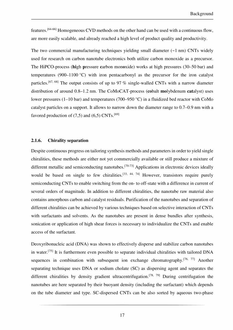
The two commercial manufacturing techniques yielding small diameter (~1 nm) CNTs widely
used for research on carbon nanotube electronics both utilize carbon monoxide as a precursor.
The HiPCO-process (high pressure carbon monoxide) works at high pressures (30–50 bar) and
temperatures (900–1100 °C) with iron pentacarbonyl as the precursor for the iron catalyst
particles.[67, 68] The output consists of up to 97 % single-walled CNTs with a narrow diameter
distribution of around 0.8–1.2 nm. The CoMoCAT-process (cobalt molybdenum catalyst) uses
lower pressures (1–10 bar) and temperatures (700–950 °C) in a fluidized bed reactor with CoMo
catalyst particles on a support. It allows to narrow down the diameter range to 0.7–0.9 nm with a
favored production of (7,5) and (6,5) CNTs.[69]
2.1.6. Chirality separation
Despite continuous progress on tailoring synthesis methods and parameters in order to yield single
chiralities, these methods are either not yet commercially available or still produce a mixture of
different metallic and semiconducting nanotubes.[70-73] Applications in electronic devices ideally
would be based on single to few chiralities.[33, 44, 74] However, transistors require purely
semiconducting CNTs to enable switching from the on- to off-state with a difference in current of
several orders of magnitude. In addition to different chiralities, the nanotube raw material also
contains amorphous carbon and catalyst residuals. Purification of the nanotubes and separation of
different chiralities can be achieved by various techniques based on selective interaction of CNTs
with surfactants and solvents. As the nanotubes are present in dense bundles after synthesis,
sonication or application of high shear forces is necessary to individualize the CNTs and enable
access of the surfactant.
Deoxyribonucleic acid (DNA) was shown to effectively disperse and stabilize carbon nanotubes
in water.[75] It is furthermore even possible to separate individual chiralities with tailored DNA
sequences in combination with subsequent ion exchange chromatography.[76, 77] Another
separating technique uses DNA or sodium cholate (SC) as dispersing agent and separates the
different chiralities by density gradient ultracentrifugation.[78, 79] During centrifugation the
nanotubes are here separated by their buoyant density (including the surfactant) which depends
on the tube diameter and type. SC-dispersed CNTs can be also sorted by aqueous two-phase

Background
18
extraction. For that two water-soluble polymers poly(ethylene glycol) (PEG) and dextran are
mixed with the nanotube dispersion and sodium dodecyl sulfate (SDS). After mixing, two phases
are formed, one rich in PEG and s-CNTs and one rich in dextran and m-CNTs.[80] The extraction
of individual CNT chiralities can be achieved in a multi-step process with carefully adjusted SDS
concentrations and was shown for small and large diameter CNTs.[81, 82]
SDS itself is also a dispersion agent for CNTs in water but does not offer any initial type or size
selection. The SDS-dispersions can however be separated by type using gel chromatography (GC)
columns with agarose gel. The degree of interaction of a nanotube with the gel is determined by
its electronic nature and diameter. Eluting a GC column – saturated with CNT dispersion – with
pure aqueous SDS, first yields a fraction rich in metallic CNTs as their interaction is weakest. The
succeeding fractions contain s-CNTs sorted by diameter. This method can thus be used to
individualize single nanotube chiralities.[83-88] The chirality purification of this method is to date
the best achievable and even enantiomer separation was demonstrated for several CNT
chiralities.[89, 90]
All of the above mentioned methods rely on non-selective dispersion of nanotubes and subsequent
separation while a centrifugation step to remove undispersed material is implemented in-between.
Nish et al. introduced an alternative concept, i.e. directly dispersing only certain chiralities in
organic solvents.[91] They used different conjugated polyfluorenes and aromatic solvents and
found the highest selectivity for CNTs from various CNT sources (e.g. HiPCO and CoMoCAT)
with poly(9,9-dioctylfluorenyl-2,7-diyl) (PFO) and poly[(9,9-dioctylfluorenyl-2,7-diyl)-alt-co-
(1,4-benzo-2,1′,3-thiadiazole)] (PFO-BT) in toluene. A largely reduced selectivity was observed
in other organic solvents such as tetrahydrofuran (THF) and chloroform. From this starting point
a vast amount of conjugated polymers was tested for dispersion selectivity including
polyfluorenes with different side chains,[92] and polyfluorene copolymers,[93-99] but also
polythiophenes,[100, 101] polycarbazoles, [96, 102] and others.[103-105] While a large number of
conjugated polymers is able to disperse CNTs, the selectivity and yield vary widely. In various
studies, the influence of solvents,[91, 98, 99, 106, 107] molecular weight,[52, 106, 108] and sidechains was
studied and guidelines for polymer and solvent selection were provided.[92, 100] An experimentally
simple one-pot method yielding nearly monochiral (6,5) dispersions was established with a
polyfluorene-bipyridine copolymer (PFO-BPy) in toluene from CoMoCAT raw material.[109]
Similar to other dispersion methods, sonication was used to debundle the raw material and support
efficient wrapping of the polymer around the nanotubes. The non-dispersed material, i.e. other

Background
19
unwrapped CNTs, amorphous carbon, catalyst, and remaining bundles were removed by
subsequent centrifugation. Recently, a method to scale up this process was introduced that relies
on shear-force mixing instead of sonication to individualize the CNTs during the wrapping
step.[110]
Conjugated polymers exhibit much lower carrier mobilities than CNTs and usually have a much
larger bandgap. Thus they do not contribute to the transport in a polymer-CNT composite but
rather impede fast hopping of charges between nanotubes. It is therefore necessary to minimize
the amount of polymer by ultracentrifugation at high centrifugal forces (> 200 000 g) in
combination with washing steps and redispersion in pure solvent of the sediment containing the
chirality selected CNTs. Alternatively, vacuum filtration can be used to reduce the amount of free
polymer.[111, 112] Further removal even of the polymer directly wrapped around the CNTs can be
realized by employing designed copolymers that decompose under certain conditions
(temperature, acid treatment) or by complexation and stripping with a Rhenium salt.[113-115]
However, even if the polymer wrapped around the CNTs is not completely removed, the coverage
should be less than 20 % and thus leave sufficient space for direct nanotube–nanotube
junctions.[44]
2.2. Carbon Nanotube Transistors
2.2.1. Overview
Transistors are three-terminal devices that control the charge transport between the source and
drain electrodes with a voltage applied at the gate electrode Vg. They require several components
deposited and structured on a suitable substrate: A semiconductor, source and drain electrodes for
charge injection and extraction into and out of the semiconductor, a gate electrode to control the
current flow through the semiconductor and a dielectric insulating the gate from the
semiconductor to prevent current flow between source/drain electrode and gate electrode.
The general performance of a field-effect transistor also depends on the device dimensions
illustrated in Figure 2.8. The distance between source and drain electrodes defines the channel
length L and the length of the electrodes defines the channel width W. The schematic figure also
shows the applied voltages Vg, Vd, and Vs. The currents at the respective electrodes are Ig, Id, and
Is. Usually, the source electrode is grounded, i.e. Vs = 0 V, and in this work the terms source–drain
voltage Vds and source–drain current Ids will be used. As the gate current Ig originates from charge

Background
20
carriers leaking through the gate dielectric, it is often also called gate leakage. The thickness of
the dielectric determines the dielectric capacitance C as well as the electric field across the
insulator. In unipolar FETs only one charge carrier type, i.e. holes or electrons, can be transported
through the channel, while ambipolar semiconductors such as carbon nanotubes are able to
conduct both charge carriers.
Figure 2.8: Important notations illustrated in a staggered top-gate transistor.
2.2.2. Device architectures
Different device architectures to realize the required order of layers are possible and each exhibit
certain advantages and disadvantages (see Figure 2.9). The two different possible stacks are
named staggered (gate–dielectric–semiconductor–source/drain) and coplanar (gate–dielectric–
source/drain–semiconductor). Depending on the position of the substrate (in contact with the gate
or not), they are further divided into bottom-gate and top-gate. In all cases, the applied gate voltage
causes a charge carrier accumulation in the semiconductor at the interface to the dielectric. While
in coplanar structures charges can only be injected into the semiconductor at the edge of the source
and drain electrodes, the staggered configuration enables charge injection also at the surface of
these electrodes thus leading to current crowding and a reduced injection barrier. During
fabrication, often rather harsh processing conditions are used: elevated temperatures during
deposition and annealing, as well as solvents and corrosive solutions for structuring, e.g. when
using photolithography. These techniques may affect the final device, especially the properties of
the semiconducting layer. The decision for top-gate or bottom-gate structures thus mainly depends

Background
21
on the processing conditions best fitting the used materials, i.e. the thermal and chemical stability,
the possibility to use orthogonal solvents, and the sensitivity of individual layers. For very
sensitive semiconductors the coplanar bottom-gate structure is most suitable as all structuring and
deposition steps are completed before the final deposition of the active material. On the other
hand, the staggered top-gate architecture improves the charge carrier injection and permits a
precise patterning of all layers including the gate and thus enables high performance transistors
when resistant dielectrics and semiconductors are used.
Figure 2.9: Device architectures for thin-film transistors: Staggered (left) and coplanar (right) stacks
with top and bottom gate.
2.2.3. Layer Deposition and Structuring
While the dielectric is usually non-structured and deposited over the whole sample, other layers
need to be structured during or after their deposition. Especially the source and drain electrodes
usually require very precise patterning as they define the final device dimensions (see Figure 2.8).
Depending on the application or planned measurements, a structured semiconductor is useful to
define the channel area more exactly, i.e. limit edge effects and reduce leakage currents through
the gate dielectric as well as cross-talk between neighboring devices. Conventional device
fabrication mainly relies on top–down processes, i.e. large-area deposition of materials and
subsequent structuring.
The deposition of conductive materials for electrodes is usually performed by evaporation or
sputtering. The material is transferred to the gas phase in both techniques and hence processing
in vacuum is required. Thermal evaporation is also used for the deposition of semiconductors,
although casting from solution ideally at ambient conditions is preferred. A wide range of

Background
22
techniques is used here, e.g. spin-coating, dip-coating, immersion, and drop-casting, depending
on the amount of material available, the required homogeneity and film thickness, and the ease of
processing. Concerning the unpatterned dielectric, a completely closed layer is essential to avoid
shorts to the gate electrode in the final devices. Often used deposition methods are spin- and dip-
coating, physical or chemical vapor deposition (PVD and CVD), or atomic layer deposition
(ALD).
Structuring of individual layers can be done by shadow masks, photolithography and subsequent
etching and/or lift-off. While shadow masks are simply placed between the sample and deposition
source, e.g. evaporation crucible, sputter target, or airbrush gun, and thus have no impact on the
layers beneath, their resolution and alignment accuracy are usually limited. In contrast to that,
very precise alignment and high resolutions (< 1 µm) can be achieved via photolithography. A
photoresist is spin- or dip-coated on the sample surface and exposed to ultraviolet light through a
chrome-on-glass mask. The exposed areas either become soluble to the subsequently used
developer due to degradation (positive resist) or they cross-link and thus become insoluble
(negative resist). The prepared structure is then used as a mask for material deposition. With the
subsequent resist removal (lift-off) the material deposited on the resist is stripped off and the
desired structures, e.g. the source and drain electrodes, are created. The resist can also be used for
patterned etching where it is protecting the covered areas. This can be used to pattern a previously
deposited (e.g. via spin- or dip-coating) semiconductor with oxygen plasma or use corrosive
materials for wet-etching of metals.
The most important disadvantages of top–down processes is the large amount of material wasted
during structuring or deposition and the necessity of structuring processes potentially harmful to
the afore deposited material. In contrast to that, printing processes inherently produce patterned
layers and hence additionally reduce the number of required processing steps (see section 2.3).
2.2.4. Unipolar Thin-Film Field-Effect Transistors – Basic Principles
In this section, an n-type transistor, i.e. electrons as charge carriers, will be described, while the
same principles apply to hole transport with the corresponding positive charge carriers.[116-118] For
calculations of the current flow in FETs, edge effects are generally ignored and the gradual
channel approximation is used as a simplification, i.e. the electric field between source and drain
(distance of several micrometers) is assumed to be significantly smaller than the electric field

Background
23
across the dielectric (thickness of usually less than 1 µm). An applied gate voltage leads to an
accumulation of mobile charges at the interface of dielectric and semiconductor. The gate voltage
has to be larger than the so-called threshold voltage Vth. This threshold voltage depends on charge
traps, impurities, dipoles, and the charge carrier density achieved for the applied gate voltages
which can be increased by increasing the areal dielectric capacitance C.[116] The number of mobile
charge carriers per unit area Qmob without any applied source–drain voltage is
VWXY = U ∙ Z! − Z[\ (2.13)
For Vds ≠ 0 V the local potential along the channel (along x) has to be taken into account, i.e.
VWXY = U ∙ Z! − Z[\ − Z$]& (2.14)
The resulting current Ids depending on the charge carrier mobility µ , the channel width W, the
local electric field F(x) and the number of mobile charge carriers is
^_` = a ∙ b ∙ VWXY ∙ c$]& (2.15)
The local electric field is defined as
c$]& = Z] (2.16)
Integrating over the whole channel length from x = 0 to x = L with V(x) from 0 to Vds results in
^_` = a ∙ Ud ∙ b ∙ eZ! − Z[\ ∙ Z_` − Z_2 f (2.17)
For Vds ≪ Vg − Vth the quadratic term of equation (2.17) can be neglected and a simplified linear
correlation results
^_` = a ∙ Ud ∙ b ∙ Z! − Z[\ ∙ Z_` (2.18)
For Vds ≥ Vg − Vth the channel is pinched off as the local potential is smaller than the threshold
voltage and a depletion zone is formed next to the drain electrode. A current flow through the
depletion zone is still possible, the current is however space-charge-limited and a further increase

Background
24
of Vds does not increase the saturation current Ids. In the saturation regime, Vds can thus be
substituted by Vg – Vth and equation (2.17) can be transformed to
^_` = a ∙ U2d ∙ b ∙ Z! − Z[\ (2.19)
The resulting overall dependence of the source-drain current on the drain voltage for a constant
gate voltage give the so-called output characteristics and is plotted in Figure 2.10.
Figure 2.10: Output characteristics for a constant gate voltage with linear and saturation regime
(left). Schematic illustrations of charge carrier accumulation in the linear regime (right, bottom) and
pinch-off point in the saturation regime (right, top).
Below the threshold voltage an exponential dependence of the current on Vg is observed until the
current reaches a minimum for Vg smaller than the turn-on voltage Von (see Figure 2.11). The
occurrence of this subthreshold-region is a consequence of interfacial traps and in an ideal
transistor Von and Vth would be identical. The threshold voltage can be determined from the x-
intercept of a linear fit of √Ids as evident from equation (2.19).
The turn-on voltage is extracted at the point where Ids gets larger than Ig as depicted in the semi-
logarithmic plot of the transfer characteristics (Ids vs Vg) in Figure 2.11.

Background
25
Figure 2.11: Determination of turn-on and threshold voltage from the transfer characteristics in semi-
logarithmic (left axis, blue curves) and linear (right axis, yellow and red curves) current scales.
2.2.5. Extraction of Device Parameters
From the measured device characteristics the main figures of merit for thin-film transistors can be
extracted from equations (2.18) and (2.19). The charge carrier mobilities µ lin and µ sat for the
linear and saturation regime, respectively, can be calculated as follows:
bijklcmVFBsFBm = ^_`Z! ∙ da ∙ U ∙ Z_` (2.20)
b`[ lcmVFBsFBm = ^_`Z! ∙ da ∙ U (2.21)
As the mobility is an often used metric to compare different semiconductors and devices, special
care should be taken with the extraction of this value.[118, 119] The apparent value of the mobility
of a semiconductor may depend on contact resistances at the electrode–semiconductor interface
as well as the exact and correct determination of the dielectric capacitance and channel length.
Contact resistance usually leads to an underestimation of the mobility value due to the decreased
effective Vds, but high contact resistances that are reduced with increasing Vg can also result in an
overestimation if the wrong part of the non-ideal device characteristics is chosen for mobility
extraction.[120] Ideally the contact resistance of a device should be accounted for by 4-point-probe
measurements to extract the intrinsic semiconductor mobility.

Background
26
The dielectric capacitance can be measured in a quasi-metal-insulator-semiconductor structure
between the gate electrode and the combined source, semiconductor, and drain electrode. Care
has to be taken that the device is turned on completely, i.e. that the semiconductor contributes to
the capacitor electrode, and a measuring frequency as low as possible is applied to obtain the static
capacitance value. While increased noise and scattering limits the low boundary of the
frequencies, the capacitance is lower at high frequencies and too high mobility values would thus
be calculated. Typical measurement frequencies are around 1 kHz, while slightly lower
frequencies would be preferable.[118] The measured dielectric capacitance has to be divided by the
respective area A, as the areal capacitance is necessary for the current equations and mobility
calculations introduced above. The capacitance can also be calculated from the plate–plate
capacitor model with the relative permittivity of the used dielectric material ϵr, the vacuum
permittivity ϵ0, and the layer thickness d:
UnFcmFp = 'q'+ ∙ r = UWs`r (2.22)
However, the electrostatic coupling and quantum capacitance of the CNT network has to be
considered for the correct determination of the areal capacitance. Using the plate–plate capacitor
model hence leads to larger deviations from the actual capacitance and the direct measurement at
the device in the on-state is preferable.[121]
Regarding contact resistances, a reliable extraction of the intrinsic mobility of the semiconductor
is only possible with knowledge of the exact potential applied at the channel. This can be extracted
via 4-point-probe measurements where the potential is measured additionally within the
channel.[44] Alternatively, the transmission-line-method allows the extraction of contact
resistances through measurements of the same homogeneous semiconductor in devices with
different channel lengths.[52, 122] In case of crystalline materials or carbon nanotubes, the effective
channel width can be significantly lower than the geometric dimension W. For CNT networks,
additionally nanotube–nanotube resistances further reduce the mobility and the extracted values
are thus not comparable to the intrinsic mobility of single CNTs.
Considering all points mentioned above, in case of carbon nanotubes, it is more appropriate to
talk about an apparent device mobility that is not an intrinsic parameter of the semiconductor
but also includes the device architecture, dimensions and semiconductor structure, i.e. the network
composition and orientation (aligned or random) as well as the CNT density. Mobilities reported

Background
27
in this work are thus always apparent device mobilities and were extracted with capacitances
measured at the channel and without taking into account contact resistances.
Besides the mobility as an important property of a transistor, the achievable channel conductance
and current densities should be considered for the evaluation of the device performance. The
on-current depends on the applied source–drain voltage and can be easily extracted from the
device characteristics. The channel-width corrected on-conductance Gon/W reported in S mm−1
can be compared more easily for devices with different geometries:
tXka lSmmFBm = ^XkZ_` ∙ a (2.23)
The current density is defined as the current flowing through a cross-section of the
semiconductor with a certain area. For the usually present lateral transport between source and
drain electrode, a realistic assumption of the channel thickness (in z-direction) is therefore
necessary. For vertical charge transport (see chapter 6), the current density is defined by the
overlap area of the electrodes between which the current is flowing in z-direction.
The subthreshold swing SS is a measure for the concentration of shallow charge carrier traps
which are limiting fast switching speeds. A small subthreshold swing is thus essential for high
frequency applications. The subthreshold swing is the inverse of the slope of the transfer
characteristic for Vg < Vth, i.e. a fast turn-on with quickly increasing currents results in a small
subthreshold swing. The subthreshold swing is given in V dec−1, i.e. the change in gate voltage
necessary to increase the current by a factor of 10.[119]
IIlVdecFBm = $log$^_`&&Z! FB ∙ log$A&dec (2.24)
A large on/off-ratio, i.e. a high difference of on-current Ion and off-current Ioff is crucial. The value
is extracted from the maximum Ion for holes or electrons and the current in the off-state. Ioff is
often limited by residual metallic nanotubes or the gate leakage Ig. Typical on/off-ratios for CNT
transistors range from 102 to more than 108, depending on the quality, i.e. semiconducting purity,
device architecture, especially regarding Ig and CNT alignment, and the bandgap of the utilized
CNTs which determines the minimum Ioff in this ambipolar semiconductor.[54]

Background
28
2.2.6. Ambipolar Field-Effect Transistors
Carbon nanotubes are one representative of ambipolar semiconductors, but also a number of
polymers,[123, 124] single crystals,[125, 126] fullerenes,[127-129] and other materials are able to transport
both charge carriers, i.e. electrons and holes.[116, 130, 131] Furthermore mixed or stacked layers of n-
and p-type semiconductors can be used to achieve ambipolar charge transport through the
transistor channel.[132, 133] Ambipolar transport is only possible, if the electrode material exhibits
a suitable work function WF to inject both charge carrier types, which is true for carbon nanotubes
due to their narrow bandgap.
In an ambipolar transistor, the electron and the hole current, both contribute to the total current
through the device.[134] The device characteristics can thus be seen as a superposition of a unipolar
n-type and a unipolar p-type transistor. In the following, the threshold voltages / mobilities for
holes and electrons are named Vth,h / µh and Vth,e / µe, respectively. The given conditions for Vds
and Vg assume that Vs = 0 V, Vds > 0 V, and Vth,h < Vth,e. Depending on the applied voltages, the
transistor characteristics can be divided into three different regimes.
(1) Unipolar electron transport: Vg > Vth,e
Only electron transport occurs in the semiconductor and contributes to the current, i.e. the
equations for unipolar behaviour (see chapter 2.2.4) remain valid:
^_` = a ∙ Ud ∙ bs ∙ eZ! − Z[\,s ∙ Z_` − Z_2 f (2.17)
(1a) For Vds < Vg – Vth,e electron transport occurs in the linear regime.
(1b) For Vds ≥ Vg – Vth,e electron transport occurs in the saturation regime.
(2) Unipolar hole transport: Vg – Vds < Vth,h
Here, only hole transport contributes to the current through the channel
^_` = −a ∙ Ud ∙ b\ ∙ eZ! − Z[\,\ ∙ Z_` − Z_2 f (2.25)
(2a) For Vds < Vg – Vth,h hole transport occurs in the linear regime

Background
29
(2b) For Vds ≥ Vg – Vth,h hole transport occurs in the saturation regime, hence (2.25) has
to be altered with Vds → Vg – Vth,h − Vds and results in
^_` = a ∙ U2 ∙ d ∙ b\ ∙ Z_` − Z! + Z[\,\ (2.26)
(3) Ambipolar transport: Vg > Vth,e and Vg – Vds < Vth,h
In the ambipolar regime both charge carriers contribute to the overall current. With holes and
electrons injected at the drain and source, respectively. This results in a series of a hole and
an electron channel and both saturation currents have to be summed up to obtain Ids:
^_` = a ∙ U2 ∙ d ∙ zbs ∙ Z! − Z[\,s + b\ ∙ Z_` − Z! + Z[\,\ (2.27)
The different operation regimes of an ambipolar transistor are illustrated in the output and transfer
characteristics in Figure 2.12. The device parameters are usually derived from the unipolar
operating regimes.
Figure 2.12: Transfer characteristics (left) and output characteristics for positive voltages (right) of
ambipolar transistors.

Background
30
2.2.7. Networks and Arrays of CNTs as Thin-Film Semiconductors
Originating from the one-dimensional structure, the charge transport properties in carbon
nanotubes exhibit a strong anisotropy. Additionally, barriers at the junctions of different CNT
chiralities but also hopping between nanotubes of the same kind further hinder the charge
transport. It is therefore important for the overall transistor performance, how many nanotube–
nanotube junctions of which barrier height have to be overcome to cross the channel, i.e. the
nanotube orientation, length, and mixture of species in the network are important. In general, four
different patterns of nanotubes constituting the semiconductor can be distinguished: individual
nanotubes, arrays of parallel CNTs, aligned networks, and random networks (see Figure 2.13).
Figure 2.13: Schematic of different CNT film structures: individual tubes, parallel arrays, aligned
networks, and random networks (left to right).
Incorporating individual CNTs into transistors requires high precision, alignment, and structuring
and is therefore limited due to the high fabrication costs involved. However, individual CNT
properties can be studied, and sub-10 nm channel lengths with very high switching speeds and
mobilities were realized.[135-137]
Directly growing aligned CNT arrays simplifies device fabrication while maintaining the
advantage of direct connections between the source and drain electrode without any junctions.
Furthermore, the arrays exhibit overall larger currents and templated growth from deposited
catalyst along surface features or external electric fields result in predictable CNT patterns that
enable fast alignment of subsequent layers to complete the devices.[61, 64, 65, 138] However, as
monochiral growth was still not achieved for a wide range of CNT species, metallic CNTs are
usually present in these devices and perturb the device performance. Additionally, high
temperatures are usually necessary and thus only a limited choice of substrates is suitable and all
other transistor layers have to be deposited afterwards.

Background
31
Solution processing of CNT dispersions is the most favorable method to deposit nanotubes for
electronics, as it opens the perspective for rather low cost fabrication methods and the possible
integration into roll-to-roll processes. However, deposition from solution results into nanotube
networks that exhibit a number of junctions along the charge transport path through the transistor
channel and do usually not show any alignment. The variety of used deposition methods ranges
from simple immersion,[50, 100, 139-141] dip-coating,[142] spin-coating,[44, 121, 143, 144] and drop
casting,[145, 146] to printed films that exhibit the advantage of direct patterning.[99, 147-153]
Certain methods can produce aligned networks of carbon nanotubes from solution. The alignment
between pre-patterned electrodes with an applied electric field during drop-casting or immersion
is called dielectrophoresis and simultaneously achieves a structured deposition at the electrode
area.[33, 154-159] Pulling a substrate out of a water reservoir with a thin layer of nanotubes deposited
on top of the liquid surface, so-called floating evaporative self-assembly (FESA) results in ribbons
of aligned CNT films.[51, 160, 161] Utilizing the coffee stain effect, nanotubes can also be aligned by
completely evaporating the solvent around a vertically oriented substrate that was initially
immersed in the CNT dispersion.[162]
Carbon nanotube transistors fabricated or annealed in inert atmosphere show balanced hole and
electron transport with comparable on-currents and mobilities within the same order of magnitude.
These properties can be preserved by encapsulation, e.g. by oxide dielectrics,[33, 163] epoxy
resin,[157] or glued class covers,[157, 159]. Without encapsulation, the CNT transistors show hole
doping due to water and oxygen adsorption when exposed to air.[164, 165]
Depending on the structure of the CNT layer, the deposition and fabrication methods, the degree
of alignment, the channel length, and the semiconducting purity of the CNT network, the range
of reported mobility values and on/off-ratios varied by several orders of magnitude. Figure 2.14
gives an overview about some of the published values and illustrates that the sole comparison of
achieved numbers is not expedient. It is instead rather important to compare the devices in the
context of their fabrication method, device architecture, and desired application. The application
is also decisive for the choice of crucial parameters: While fast switching speeds are important
for integrated circuits, display backplanes need a high stability, and large on/off-ratios are
favorable for detectors to achieve high signal-to-noise ratios. Especially printed devices often
cannot achieve outstanding numbers for all device parameters simultaneously and individual
layers as well as the complete architecture have to be optimized in the context of possible or
wanted applications.
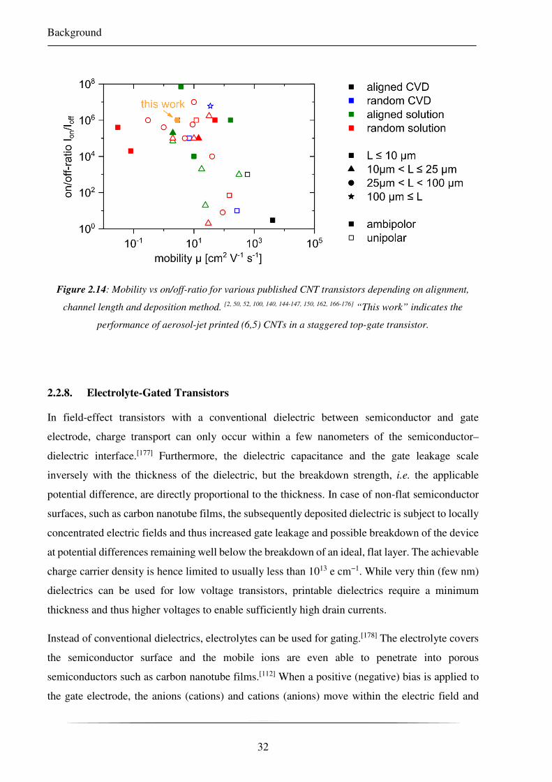
Background
32
Figure 2.14: Mobility vs on/off-ratio for various published CNT transistors depending on alignment,
channel length and deposition method. [2, 50, 52, 100, 140, 144-147, 150, 162, 166-176] “This work” indicates the
performance of aerosol-jet printed (6,5) CNTs in a staggered top-gate transistor.
2.2.8. Electrolyte-Gated Transistors
In field-effect transistors with a conventional dielectric between semiconductor and gate
electrode, charge transport can only occur within a few nanometers of the semiconductor–
dielectric interface.[177] Furthermore, the dielectric capacitance and the gate leakage scale
inversely with the thickness of the dielectric, but the breakdown strength, i.e. the applicable
potential difference, are directly proportional to the thickness. In case of non-flat semiconductor
surfaces, such as carbon nanotube films, the subsequently deposited dielectric is subject to locally
concentrated electric fields and thus increased gate leakage and possible breakdown of the device
at potential differences remaining well below the breakdown of an ideal, flat layer. The achievable
charge carrier density is hence limited to usually less than 1013 e cm−1. While very thin (few nm)
dielectrics can be used for low voltage transistors, printable dielectrics require a minimum
thickness and thus higher voltages to enable sufficiently high drain currents.
Instead of conventional dielectrics, electrolytes can be used for gating.[178] The electrolyte covers
the semiconductor surface and the mobile ions are even able to penetrate into porous
semiconductors such as carbon nanotube films.[112] When a positive (negative) bias is applied to
the gate electrode, the anions (cations) and cations (anions) move within the electric field and

Background
33
accumulate at the gate and the semiconductor, respectively. An electric double-layer (Helmholtz
layer) is formed and compensating opposite charge carriers are injected and accumulated within
the semiconductor. Due to the nm-thickness of the electric double-layer, an effective capacitance
of several µF cm−2, i.e. orders of magnitude higher than those of conventional dielectrics, can be
achieved (see device schematics in Figure 2.15).[179]
Figure 2.15: Cross-sectional view of an electrolyte-gated transistor with semiconducting CNTs and a
side-gate. The accumulation of cations and anions (red and blue, respectively) is depicted for negative
gate voltages. The electric double-layer is depicted at the gate electrode only. Holes are accumulated
in the CNT film.
A model for electrolyte-gating was described in detail by Bernards et al.,[180, 181] assuming an
electronic and an ionic circuit as shown in Figure 2.16. The electronic circuit includes current
transport through a tunable resistor Rch between the source and drain electrodes. The ionic circuit
involves capacitors at the semiconductor–electrolyte (channel capacitor Cch) and the electrolyte–
gate (gate capacitor Cg) interfaces that are connected via the electrolyte as a resistor REL. The
resistor in the electronic circuit is tuned by charging the channel capacitor as a result of the applied
gate voltage. This channel capacitor exhibits a high capacity for impermeable semiconductors and
can be described similar to FETs.[182] For porous or permeable semiconductors, the capacitance
can no longer be described by a parallel plate model but rather a volumetric capacitance has to be
used. The nm-thickness of the double-layer and even more the three-dimensional gating results in
a significantly larger charge carrier density in the semiconductor at low voltages. The source–
drain currents are hence significantly higher at comparably gate voltages of usually less than 3 V,
which was demonstrated for various semiconductors.[148, 183-186] It should be noted that
nomenclature is not consistent in literature and this type of devices is found with different names,
e.g. organic electrolyte-gated transistor (OEGT), organic electrochemical transistor (OECT),

Background
34
electric double-layer transistor (EDLT), and ion-sensitive field-effect transistor (ISFET).[182]
Often, devices with permeable or impermeable semiconductors are referred to as OECT and
OEGT, respectively.[181] The electrolyte-gated transistors described in this thesis consist of porous
CNT networks and hence enable three-dimensional gating but the ions are not expected to
penetrate inside the individual nanotubes. The electric double-layer is thus formed around the
nanotubes and the devices will be referred to as EGTs. They operate in accumulation mode, i.e.
the channel is in the off-state when no voltage is applied and charges are accumulated for transport
upon application of a gate voltage. On the other hand, devices working in the depletion mode, i.e.
ion penetration into the semiconductor leads to the compensation of fixed dopant ions and thus
reduces the channel conductivity, are also possible, e.g. with PEDOT:PSS as the
semiconductor.[181]
Figure 2.16: Illustration of electronic (bottom) and ionic (right) circuits in an electrolyte gated
transistor as adopted from literature.[181]
The high currents that can be reached in EGTs at low voltages come with the disadvantage of
rather slow response times, especially for volumetric gating. The polarization time of an
electrolyte is described by R·C, i.e. the ionic resistance of the electrolyte R and the double-layer
capacitance C. A smaller value for R·C corresponds to a faster formation of the double-layer and
hence higher switching speeds. For an electrolyte, R·C is given by
| ∙ U = A~ ∙ U = A~ ∙ 'q ∙ 'XA"~ ∙ (2.28)
where tEL is the thickness of the electrolyte, C’ the specific capacitance of the double-layer, σ the

Background
35
ionic conductivity, and tEDL the thickness of the electric double-layer.[182] In most cases, the
limiting factor for the switching speed of the device is the ionic conductivity σ, which is on the
order of 10−5 to 10−2 S cm−1. While theoretically operation frequencies in the kHz (OECTs) to
MHz (non-porous OEGTs) regime are possible, the device geometry, semiconductor thickness,
and charge carrier mobility influence the switching speed as well and often lead to longer response
times.[182] However, devices with response times fast enough for various applications, e.g. OLED
drivers and biosensors, have been reported frequently.[182, 187-192]
Electrolyte-gating has a long history going back to the first transistors by Bardeen and
Brattein.[193] The recent renaissance of practical electrolyte-gated transistors, especially in organic
electronics, started with transistors containing solid polymer electrolytes, e.g. LiClO4-doped
poly(ethylene oxide), and polyelectrolytes that exhibited rather low switching speeds due to the
strongly limited mobility of the ions within the polymer.[178, 181, 182] A replacement with ionic
liquids, i.e. salts that are liquid around room temperature, improved the switching speeds but
required a frame for containment which prevents practical applications beyond sensors.[179]
Mixing the ionic liquid with certain polymers results in ion gels that may exhibit slightly reduced
ionic mobility (with respect to the pure ionic liquids) but can be spin-coated or even printed onto
devices and form a quasi-solid layer.[194-196] The ionic liquids and gels are stable within an
electrochemical window of about ±2.5 V, depending on the utilized ions and exclusion of oxygen
and water.[179, 182] In case of mechanically stable ion-gels, the gate electrode can be placed on top
of the channels, however the ion mobility also allows to use a side-gate laterally removed from
the channel that can be structured with the source and drain electrodes which reduces the number
of processing steps.[112, 157, 197] For liquid electrolytes, a gate electrode, e.g. a platinum wire, can
also be directly inserted into the liquid.
In addition to low-voltage operation and large currents, electrolyte-gating provides further
advantages: Ion-gels can be processed from solution, the gel is inherently flexibility, and the
coverage of non-flat semiconductors and surfaces such as paper is possible without negatively
influencing the device performance.[179, 198] The thickness of the ion gel is not limiting the current
and can be large. Ion-gels are hence compatible with printing techniques and printable inks were
already demonstrated (see section 2.3). Electrolyte-gating is furthermore especially interesting for
sensing applications. Even pure water is a good electrolyte for EGTs due to its self-ionization.
Analyte molecules present in aqueous solutions can change the device characteristics, i.e. they
can alter the double-layer capacitance, the threshold voltage, the on/off-ratio, or the charge carrier

Background
36
mobility.[189] The sensing mechanism can be based on different effects. While a response of the
unmodified semiconductor to the analyte is possible, it is usually non-selective, which is
especially adverse for sensing in biological samples. Modifying the semiconductor or the gate
electrode with a receptor, e.g. an antibody for proteins or complexes for ion detection, results in
high selectivity and extremely low detection limits with a dynamic range, i.e. detectable
concentration of the analyte, of more than 5 orders of magnitude.[158, 190] Further applications of
EGTs that exceed the scope of this work include sensing of neural activity, mimicry of biological
neural networks (neuromorphic devices), and memories.[181]
2.3. Printed Electronics
2.3.1. Overview
The term printed electronics includes a wide range of materials, additive deposition techniques,
and possible applications on brittle, flexible, and eventually even stretchable substrates. The
resulting devices vary in terms of complexity, feature sizes, integration density, and requirements
concerning long-term stability, conformity, tolerances, and environmental compatibility. In
contrast to the established and market-dominating circuits based on silicon technology, flexible
and stretchable substrates require low-temperatures but could eventually enable fast and low-cost
fabrication with roll-to-roll processes, ideally in ambient environment. For transistor-based
applications, the cost-reduction of silicon devices has so far been achieved via increasing the
packing density of integrated circuits. Printed electronics on the other hand aim to combine
materials that are generally processable from solution or dispersion with rather low-cost substrates
and high-throughput fabrication methods that are not compatible with silicon technologies.
Moreover, varying designs can be realized efficiently even for small batch sizes as no fabrication
of masks is necessary.
The possible and partly already demonstrated applications cover antennas, light-emitting diodes
(LEDs), photovoltaics, individual transistors as well as integrated circuits, chemical, optical,
mechanical, and biological sensors, extending to complete RFID tags,[199] displays,[200-205] and
neuromorphic networks.[206] The following sections will give an overview about different printing
techniques and materials. In the context of this work, the main focus will be on transistors,
nevertheless including further applications.

Background
37
2.3.2. Materials for Printed Transistors
All materials used for printed transistors and circuits have to meet one common requirement, i.e.
the processability from a solution, dispersion, or paste, depending on the printing method (see
section 2.3.3). In case of flexible or stretchable substrates, the allowed (post-)processing
temperatures are additionally limited.
Conductors represent the fundamental material class of all printed electronics. The contacts of
devices, interconnects, and leads have to be free of disruptions as those would result in fatal device
damage. Depending on the application, high conductivities and suitable work functions are
necessary for charge transport and injection.[198] The utilized materials were typically either
metals, polymers, or based on carbon allotropes. The highest conductivities were exhibited by
structures printed from metallic inks which were usually based on nanoparticles, nanowires, or
metal-organic precursors.[207] An annealing step was necessary here to either remove surfactants
and dispersing agents from colloidal inks or ensure the decomposition of precursor-based inks.
Additionally, it was often necessary to sinter the deposited metal to further reduce the resistance.
Annealing and sintering were most often performed via simple heating, but other techniques based
on lasers,[208, 209] microwave or UV radiation,[210-212] and electric currents to selectively heat only
the metallic material were developed.[213] The choice of metal depends on the electrical suitability
and processing conformity, but also on the price and availability of printable inks. Currently, most
commercially available ink formulations are based on silver nanoparticles, but also gold
nanoparticles are available.[198] Transistors based on printed silver nanoparticle electrodes were
hence found most frequently,[112, 147, 151, 153, 214-228] but also examples for silver nanowires or gold
nanoparticles were demonstrated.[153, 217, 229-232] Although graphene and carbon nanotubes were
both used as electrode materials and dispersions could be prepared easily, there are only few
reports on printed transistor electrodes from these materials, probably due to the rather high sheet
resistances when compared to printed metals.[153, 233-236] Concerning polymer conductors, the
blend of poly(3,4-ethylenedioxythiophene) and poly(styrene sulfonic acid) (PEDOT:PSS) was
used most often,[149, 219, 237-240] but demonstrations of conducting polyaniline were published as
well.[198, 241] Composite materials with PEDOT:PSS and reduced graphene oxide or silver
nanowires also showed reasonable stretchability.[242, 243] Although the majority of reports used
metallic electrodes, other materials are of special interest for flexible and stretchable applications.
Polymers, nanowires, and carbon nanotubes might be used where brittle metals hit their limits and
several reports about the fabrication of stretchable electrodes – although not all of them were
printed – were published. [244-252]

Background
38
Semiconductors used in printing processes cover a wide range of especially synthesized but also
commercially available polymers, small molecules,[222, 240] metal oxides,[253, 254] and carbon
nanotubes. As most polymers can be processed from solution, they are ideal candidates for
deposition via printing and were thus widely used. Printed semiconducting layers for transistors
were shown for poly(3‐hexylthiophene) (P3HT) and several other thiophenes,[223, 232, 233, 238, 239,
255-258] but also polyarylamines and other commercial polymers were utilized.[224, 225, 237, 259] In
contrast to oxides that are usually brittle, polymers also exhibit flexibility and stretchability at
least to a certain degree and were used in stretchable transistors.[250, 260-262] The high number of
publications about printable polymers possibly originates from easier preparation of inks as most
polymers can be dissolved in suitable solvents without the necessity of additional surfactants.
Carbon nanotubes on the other hand need dispersing agents that might be detrimental to printing.
However, dispersions containing mainly semiconducting species could already be deposited by
gravure,[263, 264] aerosol-jet,[151] [149, 265] and inkjet printing.[152, 221, 266-268] The main advantage of a
semiconductor constituted of a nanotube network is the high carrier mobility while maintaining
the inherent flexibility and stretchability.[1, 269] Stretchable devices utilizing carbon nanotubes
were also presented with CNT layers created by film transfer, spin coating, drop-casting, or
immersion.[147, 227, 236, 270-276]
Dielectrics should exhibit a high permittivity as well as breakdown strength to ensure high
capacities and low leakage currents. However, the oxides widely used to fulfill these requirements
are usually not printable and hence other materials have to be utilized here. As already mentioned
with respect to semiconducting materials, polymers are most often printable and thus
polyvinylphenol (PVP), [217, 222, 223, 225] polyimide, [226] and other commercial polymers were used
in printed dielectric layers for transistors.[224, 256] Furthermore, the usually spin-coated
fluoropolymer CytopTM was deposited via inkjet and flexo printing.[240, 259] In stretchable
applications, ionic liquids and ion-gels were used widely and printing of these materials was
previously demonstrated.[148, 149, 151, 152, 233, 234, 239, 255, 277] Composites of barium titanate
nanoparticles with different polymers such as poly(methyl methacrylate) (PMMA) and
poly(dimethylsiloxane) (PDMS) were used in flexible and stretchable transistors. These materials
result in high dielectric constants of up to 17 and are commercially available.[147, 221, 227, 236, 237]
The wide range of solution-processable materials that were usually applied via spin-coating but
have the potential to be printed was subject of a current review that lists a large number of ion-
gels, polymers, polymer blends, organic/inorganic blends and bi-layers, including cross-linkable
species to prevent dissolution in subsequent fabrication steps.[278]

Background
39
State-of-the-art devices with carefully chosen materials and deposition processes already
enabled completely printed, stretchable devices. Transistors based on CNTs as electrode and
semiconductor material combined with a BaTiO3/PDMS composite dielectric were able to
withstand more than 50 % strain.[236] Although post-deposition patterning was required due to
drop casting involved in the process, the necessary masks were also printed. However, the
majority of stretchable devices still relied on additional non-printing steps. Photolithographic
patterning and metal evaporation for electrodes,[270, 273] or top-down patterning of the
semiconductor are often necessary.[236, 268, 272, 273, 275, 277] Additionally, devices or individual layers
are often fabricated on rigid substrates and later transferred to elastomers to ensure
stretchability.[268, 273, 279] An often utilized technique for increasing the stretchability is the so-
called buckling that can be achieved when pre-stretching the substrates.[270, 274, 280, 281] Layers
transferred on pre-stretched substrates buckle upon stress-release and the tolerable range of
deformation could be increased. All-printed flexible transistors were demonstrated based on
printed silver electrodes, semiconducting carbon nanotubes or small molecules, and a barium
titanate / polymer composite dielectric. For these devices, bending radii of a few millimeters down
to 140 µm when fabricated on ultra-thin substrates were reported.[147, 227, 282] However, the
majority of reports still relied on non-printing techniques for some of the deposited layers.[173, 271,
283-285] Additionally, flexible substrates were used for some completely printed devices but without
quantification of the performance stability with respect to bending.[148, 263-265, 267, 286, 287]
Although a wide range of materials that can be printed and/or stretched was demonstrated, the
majority of reports did not combine these favorable properties for all layers of the devices and
publications about all-printed, stretchable or flexible transistors are still rare. However, the
availability of materials and demonstrations of devices withstanding intensive stress, strain,
bending, or other environmental impact is promising for future applications.
2.3.3. Printing methods
One possibility to categorize printing techniques is to distinguish between contact and non-contact
methods, but also other categories such as direct-write vs using a physical mask, or batch vs roll-
to-roll processing are possible. Gravure, offset, and flexographic printing all require structured or
pretreated cylinders that come in contact with the substrate and thereby transfer the ink. Further
examples of contact printing techniques are screen printing and microcontact printing. Systems
that use masks for patterned deposition, e.g. airbrush spraying, can also be added to this category.

Background
40
The main non-contact printing methods are inkjet and aerosol-jet printing that are both capable of
directly writing the desired patterns without any masks or contact to the substrate.[198, 288-291]
High-throughput roll-to-roll printing techniques require pre-structured printing cylinders
increasing the initial costs of manufacturing. A graphical overview about some methods is given
in Figure 2.17. Flexography is a relief printing technique that uses a soft, structured roll with
elevated features to transfer the ink to the substrate. Conducting features were successfully printed
with flexography for organic photovoltaics with failure-free deposition over several 100 m.[292,
293] The main disadvantages are non-uniform heights of printed structures, swelling and elasticity
changes of the printing cylinder due to organic solvents used in the process and wear of the rather
soft material. While features are elevated in flexography, gravure printing uses pre-patterned
grooves in a hard cylinder for ink transfer. The printing results in a pixelated image on the
substrate and the individual pixels have to connect by ink flow after deposition.[294] As the solid
engraved cylinders are not deformable, a uniform contact with the substrate requires a flat surface
and this technique is hence most suitable for patterning the first layer of a device. Material
deposited before a gravure printing step can be damaged due to high mechanical pressure or lower
spots might be not in contact with the printing roll and thus hinder material transfer. Offset
printing cylinders are not three-dimensionally patterned but exhibit a difference in surface energy
of individual areas on one of the printing cylinders.[198, 290] While this technique is used frequently
in classical printing, especially the required viscoelastic properties of the ink, i.e. a very high
viscosity and a pronounced shear thinning, which can only be reached with additives, prevent a
widespread use in printed electronics. A modification of this printing process is called reverse
offset printing. The completely coated flat cylinder is here rolled over an engraved glass plate to
partially transfer the ink to elevated glass areas. The ink remaining on the cylinder is then
transferred to the substrate and enables sub-micron resolution.

Background
41
Figure 2.17: Schematic illustration of different printing methods: flexography (top left), gravure
printing (top right), offset printing (bottom left), and rotary screen printing (bottom right).
In contrast to the above mentioned methods that rely on ink transfer, other techniques use masked
deposition. Spray deposition through shadow masks can be used for various materials but results
in a high material loss due to the large areas coated during the process. Nevertheless, it was used
for various materials on the lab scale for electrodes and semiconductors in field-effect transistors,
sensors, photovoltaics and other devices.[111, 179, 295-301] The material is deposited from a dispersion
with a commercial airbrush gun and the resolution mainly depends on the used shadow masks. In
case of heated substrate stages, metal-organic precursors can form an oxide due to pyrolysis
occurring at the substrate. In the screen printing process, the ink is squeezed through a mesh that
is partially closed to form a mask. This enables the realization of unconnected patterns that are
not possible with shadow masks.[198, 290] While flatbed screen printing is a batch process, rotary
screen printing, i.e. using a patterned mesh on a cylinder, can be incorporated in roll-to-roll
processes. The current state regarding throughput, and resolution as well as examples of printed
layers for transistors are summarized in Table 2.1.

Background
42
Table 2.1: Overview of different printing techniques
Printing
technique
Max. speed
[m min−1]
Resolution
[µm]
Examples
Conductors Semi-
conductors
Dielectrics
Flexography 500 [198] 30 [198] [219, 226, 292, 293] [253, 254, 257] [219, 226]
Gravure 1000 [290] 2 [302] [147, 224, 240, 303,
304]
[219, 224, 257, 259,
303, 304]
[147, 219, 224, 257,
303, 304]
Offset 1000 [198] 20 [198] [219, 237]
Reverse offset 3 [305] < 1 [258] [258, 305, 306]
Screen 35 [307] 50 [198] [227, 233, 259, 308] [259, 308] [227, 259, 308]
Rotary Screen 100 [307] 100 [309] [309]
Spray N/A 10-100 [111, 297] [179, 298-301, 310]
Inkjet 100 [198] 10 [294] [222, 238, 266, 311-
319]
[222, 238, 256, 257,
266, 312, 320-324]
[227, 259, 308, 325]
Aerosol-jet N/A 10 [326] [152, 239, 265, 327-
330]
[148, 149, 153, 187,
192, 233, 239, 255, 265,
327-334]
[149, 187, 192, 239,
255, 329, 330]
Inkjet printing is a technique that works in the non-contact mode and does not require physical
masters for pattern creation.[335] Additionally, the required ink volumes are rather small. While
the throughput is rather low, it can be easily upscaled by parallelization, i.e. the simultaneous use
of several print nozzles, and reach printing speeds of up to 100 m min−1. The ink viscosities are
comparably low with 1–40 mPa·s and depend on the nozzle diameter.[198] The low viscosities
enable the use of highly purified materials even in low concentration without the need of
additional binders in the ink. In a typical inkjet printer, the printer head and nozzle consist of an
ink reservoir with a piezoelectric constrictor and a fine opening towards the printing substrate.
The constrictor is deflected by an applied voltage and thus generates a pressure wave that pushes
ink through the nozzle opening. The constrictor then straightens again which causes another
pressure change in the ink and a droplet is formed of the material previously pushed through the
nozzle.[294] The ejected material is hence deposited in small droplets that define the printing
resolution of down to less than 10 µm. For the creation of closed layers, the droplet spacing has

Background
43
to be small enough to result in continuous paths. Smaller droplets thus enable a higher resolution
but also decrease the throughput as the number of droplets that have to be deposited to generate a
continuous line increases. The optimum drop spacing has to be determined for each ink and nozzle
size to avoid discontinuities as well as bulges that result from too low spacing und thus too much
ink.
Conductive paths of metals,[222, 311-313] polymers,[238, 266, 314, 315] and carbon nanotubes were
prepared with inkjet printing that can serve as electrodes in transistors and photovoltaics.[316-319]
Carbon nanotubes,[266, 312, 320-324] pentacene precursor,[222, 324] oxides,[321, 323] and polymers were
printed as semiconductors for transistor applications.[238, 256] Moreover, inkjet printing of
electrodes was used in combination with dewetting structures to enable submicron channel lengths
or completely inkjet printed devices.[222, 315]
Fully inkjet-printed transistors with silver electrodes, a commercial p-type polymer
semiconductor, and PVP dielectric were demonstrated and thoroughly analyzed for device failure
causes originating from the printing process. Besides particles or material impurities, the main
failure reasons were discontinuities in electrodes or dielectrics due to nozzle clogging, and source-
drain shorts due to droplets deposited aside of the printing pattern.[225] These issues can also easily
occur in transistors utilizing printed CNTs. Carbon nanotube transistors were presented using
CNTs as electrode and semiconductor material. Specifically functionalized nanotubes were used
with a PEG dielectric in a process that does not rely on previous sorting of CNTs.[336] By tuning
the CNT coverage of unsorted CNTs, the conductivity and eventually the switching behaviour
could be tailored in an electrolyte-gated transistor with a channel length of several millimeters
with a mobility of 1–4 cm2 V−1 s−1 and an on/off-ratio of up to 105, although at very low overall
currents.[337]
In combination with other patterning or deposition techniques, inkjet printed CNTs were also
successfully used in transistors and even complimentary logic circuits. The individual transistors
exhibited mobilities of around 10 cm2 V−1 s−1 and on/off-ratios of up to 107.[221, 266]
Aerosol-jet printing is a further non-contact method successfully used for printing of various
materials, including conductors and carbon nanotubes. As this method was mainly used within
this work, it will be explained in more detail in the next section.
In the last years, various methods, materials, and devices were also the subject of several review
articles.[182, 198, 289-291, 294, 307, 326, 335, 338-343]

Background
44
2.4. Aerosol-Jet Printing
2.4.1. Working principle
Aerosol-jet printing relies on the aerosolization of a liquid ink, i.e. transferring the ink into a
nebular phase of small droplets with a size of 1–5 µm. This process can be either realized with a
pneumatic atomizer or – as utilized in this work – with an ultrasonic atomizer. The printing
process is illustrated in Figure 2.18. For ultrasonic atomization, the ink is placed into a glass vial
with a thinned bottom. The vial is closed while a gas inlet and an aerosol outlet remain open. In a
temperature controlled water bath a transducer generates ultrasonic waves with a frequency of
around 13 MHz. Through the water bath and the thin vial bottom, the ultrasonic power can be
transferred to the ink. An aerosol can be formed in the vial, if the ink has a suitable viscosity of
1–10 mPa·s. A suitable viscosity is not only important for the aerosolization process but also
influences the flow of deposited material on the substrate. Most solvents of active materials, such
as toluene for carbon nanotubes, exhibit rather low viscosities and need a highly viscous co-
solvent to reach the desired viscosity range. The aerosol is then transported with a carrier gas
through a tube attached at the aerosol outlet. The aerosol enters the printer head centrally and a
focusing gas (also called sheath gas) is added. For both, the carrier and the sheath gas, usually dry
nitrogen is used. Due to the printer head geometry, the focusing gas completely surrounds the
aerosol, so that with ideal printing conditions, no contact of the material to be deposited to the
printer nozzle occurs. Within the printer head and the nozzle, the stream is further focused to the
inner nozzle diameter which is 100–300 µm at the outlet.

Background
45
Figure 2.18: Illustration of aerosol-jet printing setup with an ultrasonic atomizer. Adopted with
permission from Adv. Electron. Mater. 2017, 3, 1700080.[150]
The aerosol stream exiting the nozzle remains focused over a distance of several millimeters and
thus enables printing on flat as well as uneven substrates without a loss of spatial resolution in
contrast to inkjet printing.[344] Because the output is continuous and not just on demand, a spoon
shaped shutter below the printer nozzle is used to control the deposition of material. In the
benchtop version of the printer used in this work, the substrate is placed on a heated stage that can
be moved automatically in the x- and y-direction. Other machines of the so-far only supplier
Optomec Inc. are equipped with a 5-axial stage or can be incorporated into roll-to-roll printing
systems.
The output volume as well as the line width, thickness, and shape are mainly controlled by the
gas flows, the nozzle size, and the stage speed. Additionally, also the stage temperature and the
ink composition influence the final printing pattern as they control the evaporation of solvents and
interaction with the substrate, and thereby the flow of deposited material on the substrate. While
too little interaction between substrate and ink can result in discontinuities of printed lines,
excessive wetting leads to a significant loss of spatial resolution. The influences of nozzle size,
stage speed, and flow rates were previously examined in detail for a silver nanoparticle ink.[345]
The line width decreased – and thereby the line thickness increased – with decreasing nozzle size

Background
46
and increasing ratio of sheath and carrier gas. This ratio was named focusing ratio and shown to
have significant importance on the printing process. An increased carrier gas flow rate at constant
focusing ratio did not lead to increased line width but only increased thickness. Additionally, the
stage speed only influenced the line width when below a certain velocity. At higher stage velocity,
when ink spreading was less important, the line width was independent of the stage speed but only
depended on the focusing ratio. The thickness of the deposited material line was however again
dependent on the stage speed. Four different line shapes were explained by this observations:
discontinuous lines (at too low carrier gas flow or too high stage speed), ill-defined edges, i.e.
flow of material out of the line shape (at too high carrier gas flow or too low stage speed),
unfocused lines (at too low focusing ratios), and optimized lines with the focusing ratio, stage
speed, and carrier gas flow adapted to each other. The printing parameters for each possible ink
must hence be optimized.
2.4.2. (Partially) Aerosol-Jet Printed Devices
One main focus of aerosol-jet printing was the creation of conducting pathways, especially
utilizing silver nanoparticle based inks. Besides simple conductive paths and electrodes,[5, 152, 265,
327, 328, 346-349] grid-shaped and thus semi-transparent electrodes as indium tin oxide substitutes in
photovoltaics and LEDs were reported.[350-352] With fast-drying inks, even the creation of three-
dimensional structures and interconnects is possible. Additional conductive structures as
electrodes were fabricated using PEDOT:PSS.[187, 239, 327, 329, 330, 353] With regard to semiconducting
materials, devices with carbon nanotubes,[148, 149, 153, 265, 328, 331-334] P3HT,[187, 192, 233, 239, 255, 327, 330]
and oxides were demonstrated. [327, 329] Aerosol-jet printed ion-gels were presented as dielectrics
that also support flexibility and stretchability of the resulting devices.[149, 187, 192, 239, 255, 329, 330]
The so far demonstrated completely aerosol-jet printed transistors relied on established materials,
i.e. silver, PEDOT:PSS, CNTs, and ion-gels.[151, 334, 354] Usually aqueous CNT inks were used that
were not previously enriched in semiconducting species. In contrast to that, Zhao et al. dispersed
the nanotubes with 2,2-azobisisobutyronitrile in dimethylformamide.[334] Due to the presence of
predominantly semiconducting species, they were able to achieve on/off-ratios of up to more than
103 for a majority of their devices. Further publications on aerosol-jet printed transistors used
photolithographically patterned source and drain electrodes and were hence not all-printed but
resulted in improved device characteristics with on/off-ratios of up to 105 and mobilities of around
10 cm2 V−1 s−1.[148, 149] In a study comparing different aerosol-jet printed electrodes (gold, silver,

Background
47
and carbon nanotubes) with aerosol-jet printed semiconducting CNTs, an oxide-covered silicon
substrate was used as a common bottom-gate.[153] Although the number of reports is still low, it
was already demonstrated that aerosol-jet printing can be a suitable fabrication techniques for all
layers of a transistor.
Besides transistors, aerosol-jet printing was also used as the sole manufacturing technique for
photodiodes,[355] photodetectors,[356] sensors,[357] as well as band-pass and polarization filters.[358]
Additionally, active layers in solar cells were printed.[359] The range of printable materials exceeds
electronic components and reaches up to photoresist and biomolecules.[360-362]
In conclusion, aerosol-jet printing was proven to be a versatile tool for the deposition of numerous
materials on a wide range of substrates that do not necessarily have to be completely flat. With
respect to carbon nanotubes, printing was successfully used for the fabrication of semiconducting
layers in transistors. As a wide range of materials was already printed, (area selective) doping and
the addition of analyte materials can probably be realized via aerosol-jet printing. The flexible
pattern design of the additive manufacturing process further allows a fast evaluation of new
architectures and the combination of materials that is not possible with conventional fabrication
techniques.

48

49
CHAPTER 3
3.EXPERIMENTAL
This chapter details the experimental procedures performed
to obtain the results presented in this work.

Experimental
50
3.1. Alterations to the Optomec Aerosol-Jet System
In this work, aerosol-jet printing was widely used to deposit CNTs as well as metallic electrodes.
Aerosol-jet printing systems are manufactured by Optomec Inc., Albuquerque, NM, United
States. Within this work, their benchtop Aerosol Jet 200 system equipped with an ultrasonic
atomizer was used. The delivered version of this system came with a sophisticated atomizer unit
that was developed by Optomec. As shown in Figure 3.1, the ink vial is placed in a small water
bath with continuous water flow and cooling via a heat exchanger. The position of the vial is fixed
within the water bath enabling reproducible sonication strength for a defined flow, water level,
and current through the ultrasonic transducer.
Figure 3.1: Aerosol Jet 200 atomizer unit.
In the original system, the ink vial is screwed into a holder consisting of several parts that also
contain the carrier gas inlet, a stainless steel pickup-tube for the aerosol outlet, and sealing rings
(see Figure 3.2). The disadvantage of this system is the labor intensive cleaning that is necessary
when switching between different inks, especially when changing from conductive to
semiconducting materials where contamination has to be avoided. The holder system was hence
customized to reduce the number of fixed parts that are used with every ink. The adapted holder
could be equipped with single-use components, i.e. modified glass pipettes for the gas inlet and
outlet that were punched through the sealing membrane of the ink vial cap. These alterations were
based on earlier systems manufactured by Optomec. With this configuration, only the printer head
and nozzles are contaminated with ink and have to be cleaned after each printing process. This

Experimental
51
modification also enabled a quick change of materials and consecutive printing of different inks
for electrodes and semiconductors with reduced down-time for cleaning.
Figure 3.2: Photographs of the original (top) and customized (bottom) vial holders depicting all
individual parts (left) and the completely assembled holders (right). The customized holder enables the
use of disposable parts directly in contact with the ink.
During the process, the created aerosol is transported from the atomizer unit to the printer head
that is mounted with the process camera and the alignment camera on a joint unit that can be
moved in z-direction. Both cameras can be focussed individually and enable the observation of
the printing process as well as alignment of the printer head to previously created patterns on the
substrate. For the realization of versatile patterns, the system was equipped with a heated stage
(maximum temperature 100 °C) that could be moved in x- and y-direction with a precision in the
micrometer range and a shutter below the printing nozzle (see Figure 3.3).

Experimental
52
Figure 3.3: Close-up photograph of the stage area of the aerosol-jet printer. A substrate is placed on
the movable stage; the distance to the printer nozzle is several millimeters. The shutter can be seen
below the printer head and nozzle. The alignment camera is visible in the right part of the image.
3.2. Device Fabrication
3.2.1. Carbon Nanotube Dispersions
Dispersions of semiconducting (6,5) carbon nanotubes were prepared with the polymer-wrapping
method.[94] First, 0.5 g L−1 of poly[(9,9-dioctylfluorenyl-2,7-diyl)-alt-co-(6,6′-(2,2′-bipyridine))]
(PFO-BPy) were dissolved in anhydrous toluene. The CoMoCAT carbon nanotube raw material
(diameter range 0.6–1.1 nm) was added at a concentration of 0.38 g L−1. Instead of the more
widely used sonication to debundle the nanotubes to facilitate efficient polymer-wrapping of
individual CNTs, a shear force mixer was used for 72 hours at 10 230 rpm.[110] Undispersed
material, i.e. amorphous carbon, left-over catalyst and other CNT chiralities, was removed by
centrifugation at 60 000 g for 45 min. The collected supernatant contained wrapped nanotubes as
well as excess polymer. This polymer was removed either by pelletizing the CNTs via
centrifugation at 268 400 g for 20 hours or vacuum filtration through a poly(tetrafluoroethylene)
(PTFE) filter (pore size 0.1 µm) and subsequent washing with tetrahydrofuran (THF). The filter
cake or centrifugation pellet were redispersed in fresh toluene by 30–60 min bath sonication
immediately prior to further use.
During a repair-related down-time of the shear force mixer, the dispersion process had to be
altered. The polymer was dissolved in toluene at 80 °C at a concentration of 2 mg mL−1. After

Experimental
53
cooling down, 1.5 mg mL−1 of nanotube raw material were added and the dispersion was bath
sonicated for 90 min. The dispersion was then centrifuged at 60 000 g for 45 min to remove
undispersed material and CNT bundles. The supernatant was collected and again centrifuged with
the same parameters. Removal of excess material was realized by pelletizing the polymer-
wrapped nanotubes at 284 600 g for 20 hours. The pellet was then washed and redispersed in fresh
toluene as described for the filter cakes above. Note that sonicated nanotubes are generally shorter
than shear-force mixed CNTs.[110]
Dispersions of mixed semiconducting and metallic carbon nanotubes as electrode material were
produced in a different way. The raw material used was TUBALL CNTs with a diameter range
of 1.2–2.0 nm. They are produced on a large scale and at low cost. Non-selective dispersion of
CNTs can be achieved by sodium cholate in water. 1 g L−1 TUBALL CNTs were added to an
aqueous solution of sodium cholate (6 g L−1). The debundling and dispersion of the CNTs was
induced by bath (1 h), tip (15 min, taper tip, 20 % power, 1 s on/off cycles) and further bath (1 h)
sonication. The removal of undispersed material was realized by centrifugation at 2970 g for
90 min. The resulting dispersion was diluted 1:224 with 2 g L−1 sodium cholate in DI water,
filtered (PTFE, 5 µm pore size) and further diluted (1:1 in DI water). This dispersion was directly
used for spray-coating as is.
3.2.2. Electrode Patterning
Four different types of electrodes were used for this work: evaporated metal, aerosol-jet-printed
silver nanoparticles, airbrush-sprayed TUBALL nanotubes, and inkjet-printed gold nanoparticles.
While the printed electrodes were already patterned, evaporated or sprayed electrodes required
additional structuring by photolithography or shadow masks.
The easiest patterning method is the use of stainless steel shadow masks. However, these masks
are usually limited to feature sizes of several tens of micrometers. They were used for airbrush-
spraying of TUBALL electrodes as well as thermal evaporation of silver gate electrodes and gold
source, drain and side-gate electrodes.
Photolithography was used as a precise and reliable patterning technique with high resolution
(≤ 1 µm) and accuracy especially for interdigitated source and drain electrodes. Each layer of the
double layer resist (LOR5B and S1813) was spin-coated at 3000 rpm for 30 s and annealed at
185 °C for 4 min or 115 °C for 1 min, respectively. Chromium-coated soda lime masks were used

Experimental
54
for patterned UV exposure with a mask aligner at a dose of 182 mJ cm−2. The samples were then
developed in MF319 Developer for 20–25 s, rinsed with deionized water and blown dry. During
exposure, the positive photoresist S1813 became soluble at the exposed areas and could be
removed in the developing step. LOR5B is not photoactive and was removed when exposed to
the developer, i.e. after selective S1813 removal, LOR5B was removed in the same areas and
additionally an undercut was realized. The undercut was beneficial to improve the lift-off of the
subsequently evaporated metals at the structure edges. The process was completed by dissolving
the unexposed photoresist (and lift-off of the metal layer on top of it) in N-Methyl-2-pyrrolidone
(NMP) leaving metal only in the areas defined by the UV exposure.
Metal evaporation was performed in an electron-beam or thermal evaporator at pressures lower
than 1·10-6 mbar and deposition rates of 0.1 to 1.0 Å s−1. The typical electrode thickness was
30 nm. When gold was used as a bottom electrode, a 2 nm chromium adhesion layer was
evaporated first. Top electrodes were evaporated directly onto the device.
Gold nanoparticles were inkjet printed by Martin Held at the InnovationLab, Heidelberg,
Germany, from a commercial ink based on a mixture of water and ethylene glycol. The PEN
substrate was rubbed with isopropanol for homogenization immediately before printing and
placed on the printer stage heated to 60 °C. The side of the substrate that was not pre-treated by
the manufacturer was facing upwards. The ink was printed as received from 1 or 10 pL cartridges
with a drop spacing of 10–20 µm. The jetting frequency and the tickle control (used to prevent
nozzle clogging while not jetting) were both set to 1 kHz while the distance between substrate and
printer nozzle was 750 µm. The printing pattern was optimized to reach an optimal trade-off
between deposition time, resolution, ink consumption, and resistivity. Hence, the wider leads
(325 µm) and the contact pads were printed as a single layer with a drop spacing of 10 µm. The
ends of the leads were triangular in shape to improve the connection to the narrower contacts. The
actual top and bottom contacts were printed with only 5 adjacent lines but 10 layers on top of each
other to reduce the overall resistance, resulting in a total width of 70–100 µm. The contact pads,
leads, and contacts of the bottom electrode were printed before deposition of CNTs in vertical
transistors, while the leads and contacts of the top electrode were printed afterwards. Refer to
Figure 7.1 for the printing pattern used with inkjet printed gold. After each inkjet printing process,
an annealing step at 155 °C in ambient air for several hours was performed to reduce the resistance
of the printed gold nanoparticles.

Experimental
55
For aerosol-jet printing of silver nanoparticles, a commercial ink was used as purchased. In
principle, the same process as described for CNTs (see chapter 3.2.3) was used while some
parameters had to be adjusted. The maximum sonication power (~ 550 mA transducer current)
was used and the temperatures of ink and stage were set to 20 °C and 100 °C, respectively. A
150 µm inner diameter nozzle was chosen and the sheath and carrier gas flow rates were set to 50
and 40 sccm, respectively. The stage speed was set to 5 mm s−1 and single lines were printed with
2 passes to form the electrodes. The contact pad was formed by parallel lines with a pitch of 50 µm
and had an approximate size of 1 x 1 mm2. The gate electrode was printed likewise and had a total
size of 15 x 1.5 mm2. Figure 3.4 illustrates the printing pattern used for VEGTs with silver ink.
The ink was annealed at 130 °C overnight in air after each printing step before further processing.
Figure 3.4: Electrode structure used for aerosol-jet printing of silver nanoparticles as electrodes in
vertical electrolyte-gated transistors including the depiction of printed CNTs (purple).
3.2.3. Aerosol-Jet Printing of CNTs
Inks of polymer-wrapped CNTs were prepared from pellets or filter cakes redispersed in fresh
toluene. The concentration of the dispersion was determined via UV-VIS-NIR absorbance
spectroscopy. The final ink usually contained 5 % v/v terpineol and the concentration was
adjusted to the desired level of 1.8 to 6.6 mg L−1 by addition of toluene.
Details of the commercial aerosol-jet printing system and alterations for a more convenient usage
in the lab with different materials are described in section 3.1. The ink vial was filled with 1 mL
of ink and the gas inlet and outlet were connected tightly. All O-rings at the printer head were
freshly greased directly before the assembly. The printing head was equipped with a 200 µm inner
diameter ceramic nozzle. The ink and stage temperatures were set to 20 and 100 °C, respectively.

Experimental
56
The ink was aerosolized at maximum sonication power, i.e. the displayed transducer current was
around 550 mA. Sheath and carrier gas flow rates (both nitrogen) were set to 30 and
(15 ± 1) sccm, respectively. The stage speed was set to 0.5 mm s−1. The lateral position and focus
of the process camera were adjusted to the output position of the aerosol stream on a silicon
substrate. The silicon substrate was chosen due to better visibility and higher contrast of the
printed lines and thus easier alignment. After focus adjustment of the alignment camera, its
position was aligned to the printing output point with the respective software tool by printing a
cross. The AJ printer was then ready to use.
The printing pattern was defined via Autodesk AutoCAD and the VMTOOLS-Plugin provided
by Optomec. The desired printing lines were drawn and the resulting toolpath was exported. Note
that the printing sequence directly depends on the drawing or insertion sequence in the AutoCAD
file. Thus the order of printing could be manually controlled. The positions of alignment markers,
so-called fiducials, had to be manually inserted into the output file before loading this file in the
printer software and enabled the alignment to previously deposited layers.
Depending on the actual substrate thickness, which varied from the silicon chip thickness used
for alignment, the vertical position of the printer head and camera unit was adjusted. This was
achieved by bringing the substrate into the focus of the alignment camera with the z-axis
micrometer screw of this unit and not with the focus screw of the microscope. With the built-in
fiducial manager, the positions of alignment markers or structure edges to the fiducials defined in
the toolpath were set and the software performed an angle correction of the printing path.
The printing itself was then performed automatically while droplet formation in the aerosol-tube
was observed and avoided. When droplets reach the printer head, a large splash on the substrate
occurs, which is especially detrimental for precise structures such as electrodes. For CNT films,
those splashes usually did not influence the devices as only little nanotube material was deposited
outside the desired printing areas.
After printing, the CNT film was allowed to settle for at least 30 min on the stage to avoid
accidental removal during subsequent rinsing with THF and IPA as well as drying with nitrogen.
Note that the terpineol did not evaporate and had to be washed off. If further processing was
carried out in inert atmosphere, the samples were annealed in nitrogen at 300 °C for at least 30 min
to remove residual water and solvents.
Experimental
57
3.2.4. Airbrush Spraying of TUBALL Nanotubes
Airbrush spraying was performed for TUBALL nanotube dispersions as electrode material. A
commercial airbrush system equipped with a 150 µm inner diameter nozzle was used. The carrier
pressure, and needle displacement were set to 1 bar and 300 µm, respectively. At a throwing
distance of 100 mm, 2 mL of the dispersion were sprayed through stainless steel shadow masks.
The masks were attached to the home-built substrate stage that was heated to 140 °C. A
homogeneous material deposition was ensured by shuttling the stage over the whole substrate
length of 25 mm. Removal of the sodium cholate surfactant was realized by soaking in deionized
water overnight. Finally, the sprayed electrodes were annealed in air at 100 °C for 30 min.
3.2.5. Fabrication of Transistors
Different transistor structures were fabricated in the framework of this thesis. For lateral field-
effect transistors as utilized in chapter 5, a staggered top-gate structure was used. Bottom
electrodes, i.e. interdigitated source and drain, were photolithographically patterned on glass
substrates. Subsequently, the semiconductor was deposited via spin-coating or aerosol-jet
printing. The hybrid dielectric consisted of a bilayer of spin-coated poly(methyl methacrylate)
(PMMA) and hafnium oxide. An 11 nm thick PMMA layer was created by spin-coating from an
n-butylacetate solution (6 g L−1) at 3000 rpm s−1 for 30 s in nitrogen atmosphere. After annealing
at 80 °C for 30 min, the samples were directly transferred into the atomic layer deposition (ALD)
chamber. After a 60 min annealing step at 100 °C in the chamber under 20 sccm nitrogen flow,
alternating pulses of tetrakis(dimethylamino)hafnium (TDMAH) and deionized water formed the
oxide layer. A thickness of 61 nm was reached after 500 deposition cycles. The transistors were
completed by thermal evaporation of the silver gate (30 nm thickness).
For vertical transistors, the bottom (source) electrode together with the side gate were patterned
via photolithography or shadow masks and consisted of 2 nm chromium and 30 nm gold. A thick
CNT film was aerosol-jet printed on the electrodes. The pattern was chosen in a way that
deposition took place with an additional margin of 100 µm around the electrode overlap area. The
top (drain) electrode was then thermally evaporated through a shadow mask (gold, 20 nm
thickness). Alternatively, all electrodes were directly aerosol-jet or inkjet printed from silver or
gold nanoparticle inks, respectively. As a third electrode fabrication method, airbrush spraying
through shadow masks was used. After deposition of the top electrode, the ion-gel was spin-coated

Experimental
58
at 100 rpm s−1 for 60 s. on top of the device. The ion-gel was prepared from [EMIM][FAP] as the
electrolyte, P(VDF-HFP) as the polymer binder, and acetone in a mass ratio of 4:1:14.
3.3. Characterization
3.3.1. Absorption Spectroscopy
Absorbance measurements were usually performed on dispersions in cuvettes with an optical path
length of 1 cm. The silicon and InGaAs detector of the spectrometer enabled acquisition in the
ultraviolet, visible, and near-infrared range and spectra were acquired in the range of 1600–
300 nm. All recorded spectra were background corrected by the measurement of a baseline with
pure solvent in the same cuvette. Optically dense films were measured with a solid sample holder.
The baseline correction was performed with a cleaned substrate.
3.3.2. Profilometry
Profilometer data was recorded to determine the thickness of printed films of carbon nanotubes,
silver nanoparticles, and gold nanoparticles. A line scan across the whole feature was acquired
and the feature height was averaged in the plateau region. Moreover, the thickness of evaporated
metals and atomic layer deposited oxides was determined by scans at the edge of sharp features.
3.3.3. (Conductive) Atomic Force Microscopy
Topography images were recorded with an atomic force microscope (AFM) in tapping or
ScanAsyst mode (Bruker) with suitable AFM tips. The resulting images were corrected with
Gwyddeon 2.41 to level backgrounds, line errors, offset and z-range. The PeakForce TUNA mode
(Bruker) was used for conductive AFM measurements. A sample bias of 1 V was applied to the
conductive tip. The resulting contact current images were normalized to the absolute current
maxima to account for varying tip conditions, peakforce setpoint, and amplitude.
3.3.4. Scanning Electron Microscopy
When possible, electrodes of the partially completed devices were grounded to the sample holder
in the scanning electron microscope (SEM) to reduce sample charging. Images were recorded
with the inLens-detector in secondary electron mode at a low acceleration voltage of 1 kV to avoid
film damage.

Experimental
59
3.3.5. Raman Spectroscopy
Raman spectra and maps of CNT films were collected with resonant laser excitation at 532 nm
with a confocal Raman microscope in back scattering configuration with a high-speed encoded
sample stage and using different objectives. Additional spectra (RBM region of CNTs) were
recorded under 633 nm excitation at various spots to reveal further CNT chiralities. Doping of
electrolyte-gated CNT films was investigated by mapping the G+-band in the whole channel using
the Renishaw Streamline mode with a step size of 1.3–2.0 µm while the source and drain
electrodes were grounded and a bias was applied to the gate electrode with a semiconductor
parameter analyzer.
3.3.6. Electrical Characterization
Device capacitances were measured with an impedance spectrometer directly on the respective
field-effect transistor. The short-circuited source and drain electrodes as well as the CNTs
constituted the bottom electrode of a capacitor, and the gate the top electrode. The measurements
were performed in the on-state of the transistor, i.e. at sufficiently high bias of ±8 V, and at a
frequency of 1 kHz.
Current–voltage characteristics with applied gate voltage (output and transfer characteristics)
were measured with a semiconductor parameter analyzer or a source-meter unit in different
voltages ranges with different sweep rates as given in the respective representations of acquired
data. Measurements without a gate were performed for the determination of the channel resistance
with a source-meter unit in a voltage range of ± 1 V.
The response to deformation of flexible transistors was determined by manually bending the
samples around metal rods of different diameters (see Figure 3.5) and contacting the devices in
the bent state. For repeated bending, the samples were attached to a home-built and automated
machine. The original purpose of this machine was isotropic stretching of samples and the design
was adapted from a formerly available commercial setup.[363] The samples were glued to
laminated paper to enable attachment to the stretching setup and ensure bending of the transistor
area. A software programme written by Peter Jeschka enabled repeated deformation between pre-
set positions (see Figure 3.5).

Experimental
60
Figure 3.5: Measurement of flexible transistors: Bending around metal rods with different diameters
(left) and automated repeated bending cycles (right).
61
CHAPTER 4
4.MATERIALS AND DEVICES
This chapter describes the materials and devices that were
used in this work.

Materials and Devices
62
4.1. Materials
The following tables give an overview about the materials used for this work:
˗ Table 4.1: Carbon nanotube dispersions
˗ Table 4.2: Photolithography
˗ Table 4.3: Metals
˗ Table 4.4: Dielectrics
˗ Table 4.5: Substrates
˗ Table 4.6: Other materials
Table 4.1: Carbon nanotube dispersions
Material Supplier Item / Specifications
CoMoCAT carbon nanotubes,
final devices
CHASM Advanced
Materials Inc., Canton, MA,
US
SG65i-L58
diameter 0.7–1.0 nm
CoMoCAT carbon nanotubes,
initial tests
Sigma-Aldrich GmbH,
Steinheim, Germany
Item no. 704148
TUBALL carbon nanotubes OCSiAL,
Leudelange, Luxembourg
black powder
supplied free-of-charge
Poly[(9,9-dioctylfluorenyl-2,7-
diyl)-alt-co-(6,6′-(2,2′-
bipyridine))] (PFO-BPy)
American Dye Source,
Baie d’Urfé, QC, Canada
ADS153UV,
MW = 34 kg mol−1
Sodium dodecyl sulfate (SDS) Sigma-Aldrich GmbH,
Steinheim, Germany
BioReagent grade, ≥ 98.5 %
Centrifuge tubes Beckman Coulter GmbH,
Krefeld, Germany
Polypropylene tubes 50 ml,
Polyallomer tubes 15 ml
PTFE filters Merck KGaA,
Darmstadt, Germany
Omnipore JVWP, pore size
0.1 µm, hydrophilic

Materials and Devices
63
Table 4.2: Photolithography
Material Supplier Item / Specifications
LOR 5B micro resist technology
GmbH, Berlin, Germany
MicroChem LOR5B used as
undercut layer
S1813 micro resist technology
GmbH, Berlin, Germany
Microposit S1813 G2
Positive Photoresist
MF-319 micro resist technology
GmbH, Berlin, Germany
Microposit MF-319
Developer, active ingredient:
Tetramethylammonium
hydroxide
Photomasks Compugraphics Jena
GmbH, Jena, Germany
Chrome on soda lime masks,
5“ x 5“ x 0.09“ mask size,
feature tolerance 0.1 µm,
≤ 0.2 defects cm−1
Table 4.3: Metals
Material Supplier Item / Specifications
Chromium for evaporation Kurt J. Lesker Company
Ltd., Hastings, England
granules, 99.6 % purity
Gold for evaporation ESG Edelmetall-Handel
GmbH & Co. KG,
Rheinstetten, Germany
granules, 99.99 % purity
Gold nanoparticle ink C-Ink Co., Ltd.,
Akahama, Japan
Dry Cure Au-J 1010B
Silver for evaporation Umicore AG & Co. KG,
Hanau, Germany
pellets, 99.99 % purity
Silver nanoparticle ink Clariant AG,
Muttenz, Switzerland
EXPT Prelect TPS 50

Materials and Devices
64
Table 4.4: Dielectrics
Material Supplier Item / Specifications
Poly(methyl methacrylate)
(PMMA)
Polymer Source Inc.,
Dorval, QC, Canada
Syndiotactic
MW = 350 kg mol−1
Tetrakis(dimethylamino)hafnium
(TDMAH) – HfOx precursor
Strem Chemicals Inc.,
Bischheim, France
Item no. 72-8000,
>98 %
1-Ethyl-3-methyl-imidazolium-
tris(pentafluoroethyl)-trifluoro-
phosphate ([EMIM][FAP])
Merck KGaA,
Darmstadt, Germany
high purity grade
Poly(vinylidene fluoride-co-
hexafluoropropylene) (P(VDF-
HFP))
Sigma-Aldrich GmbH,
Steinheim, Germany
MW ≈ 400 kg mol−1
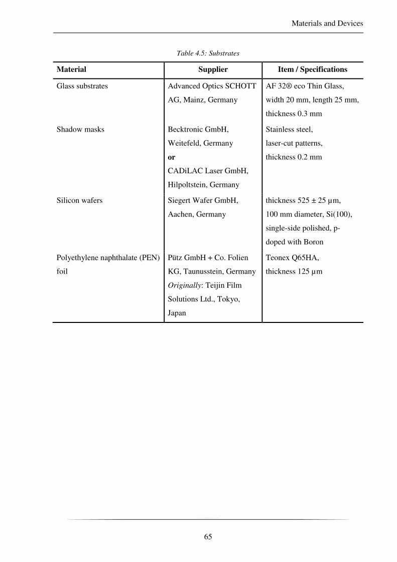
Materials and Devices
65
Table 4.5: Substrates
Material Supplier Item / Specifications
Glass substrates Advanced Optics SCHOTT
AG, Mainz, Germany
AF 32® eco Thin Glass,
width 20 mm, length 25 mm,
thickness 0.3 mm
Shadow masks Becktronic GmbH,
Weitefeld, Germany
or
CADiLAC Laser GmbH,
Hilpoltstein, Germany
Stainless steel,
laser-cut patterns,
thickness 0.2 mm
Silicon wafers Siegert Wafer GmbH,
Aachen, Germany
thickness 525 ± 25 µm,
100 mm diameter, Si(100),
single-side polished, p-
doped with Boron
Polyethylene naphthalate (PEN)
foil
Pütz GmbH + Co. Folien
KG, Taunusstein, Germany
Originally: Teijin Film
Solutions Ltd., Tokyo,
Japan
Teonex Q65HA,
thickness 125 µm

Materials and Devices
66
Table 4.6: Other materials
Material Supplier Item / Specifications
Terpineol,
CAS Number 8000-41-7
Sigma-Aldrich GmbH,
Steinheim, Germany
Mixture of isomers,
anhydrous
Other solvents
Merck KGaA,
Darmstadt, Germany, or
Sigma-Aldrich GmbH,
Steinheim, Germany
Analytical grade
Deionized water In-house, directly from
water purification system
Ultra-pure water,
R ≥ 18 MΩ cm
4.2. Devices
The following tables give an overview about the materials used for this work:
˗ Table 4.7: Carbon Nanotube dispersions
˗ Table 4.8: Device Fabrication
˗ Table 4.9: Characterization

Materials and Devices
67
Table 4.7: Carbon Nanotube dispersions
Device Manufacturer Type
Centrifuge, > 60000 g Beckman-Coulter GmbH,
Krefeld, Germany
Optima XPN-80
ultracentrifuge with swing-
bucket rotor
Centrifuge, ≤ 60000 g Beckman-Coulter GmbH,
Krefeld, Germany
Avanti J-26XP
ultracentrifuge
Glovebox for chemicals MBraun Inertgas-Systeme
GmbH, Garching, Germany
LabStar
Shear-Force Mixer Silverson Machines Ltd.,
Chesham, UK
L5M-A or L2/Air equipped
with screw-on general
purpose disintegrating head
and square hole high shear
screen
Tip Sonicator Sonics & Materials Inc.,
Newtown, CT, US
Vibra-Cell VCX-500
Ultrasonication Bath Branson Ultrasonics,
Danbury, CT, US
Ultrasonic Cleaner 2510
Ultrasonication Bath Bandelin electronic GmbH
& Co. KG, Berlin, Germany
Sonorex Digitec DT 102 H
Vacuum Filtration Merck KGaA,
Darmstadt, Germany
Merck Millipore glass filter
holders (XX1004730 or
XX1002530), vacuum
filtering flask (XX1004705
or XX1002505), and
chemical duty membrane
pump (WP6122050)

Materials and Devices
68
Table 4.8: Device Fabrication
Device Manufacturer Type
Aerosol-jet printer Optomec Inc.,
Albuquerque, NM, US
AJ 200
Atomic layer deposition
(ALD)
Ultratech / Cambridge
NanoTech, Waltham, MA,
US
Savannah S100
Evaporator, e-beam Winter Vakuumtechnik
GbR, Steinheim, Germany
HVB-130
Evaporator, thermal MBraun Inertgas-Systeme
GmbH, Garching, Germany
MB-ProVap-3
Glovebox for processing MBraun Inertgas-Systeme
GmbH, Garching, Germany
MB200G
Inkjet printer Fujifilm Holdings K.K.,
Tokyo, Japan
Dimatix Materials Printer
DMP-2889
Mask aligner SÜSS MicroTec AG,
Garching, Germany
MA/BA6 Gen4 or
MA/BA6 Gen2
each with Hg lamp (350 W)
and i-line bandpass filter
Spin-coater (for CNTs) Laurell Technologies,
North Wales, PA, US
WS-400BZ-6NPP-Lite
Spin-coater (for dielectrics) MBraun Inertgas-Systeme
GmbH, Garching, Germany
MB-SC-210
Spin-coater (for photoresist) Obducat Europe GmbH,
Lund, Sweden
EL S 200 BM
(Former solar-semi GmbH)

Materials and Devices
69
Table 4.9: Characterization
Device Manufacturer Type
Atomic-force microscope
(AFM)
Bruker Corporation,
Billerica, MA, US
Dimension Icon
AFM tips for c-AFM Bruker Corporation,
Billerica, MA, US
SCM-PIT
AFM tips for tapping and
ScanAsyst mode
Bruker Corporation,
Billerica, MA, US
ScanAsyst-Air, TESPA-V2,
OTESPA-R3
Impedance Spectrometer Solartron Analytical,
Farnborough, UK
ModuLab XM MTS
Optical microscope Olympus Corporation,
Tokyo, Japan
BX51, polarizers, bright
field and dark field available
Glovebox for electrical
measurements
Inter Corporation,
Amesbury, MA, US
IL-3GB
Profilometer Bruker Corporation,
Billerica, MA, US
DektakXT Stylus Profiler
Raman spectrometer Renishaw plc,
Wotton-under-Edge, UK
inVia Reflex confocal
Raman microscope
Scanning-electron microscope
(SEM)
Jeol Ltd.,
Akishima, Japan
JSM-7610F
Semiconductor Parameter
Analyzer
Keysight Technologies Inc.,
Santa Rosa, CA, US
Agilent 4156 C
Semiconductor Parameter
Analyzer
Keysight Technologies Inc.,
Santa Rosa, CA, US
B1500A
Source-Meter Unit Keysight Technologies Inc.,
Santa Rosa, CA, US
Agilent B2902A
Source-Meter Unit Tektronix Inc.,
Beaverton, OR, US
Keithley 2400
UV-vis-NIR spectrometer Agilent Technologies Inc.,
Santa Clara, CA, US
Cary 6000i (Varian Inc.)

70

71
CHAPTER 5
5.AEROSOL-JET PRINTING OF
CARBON NANOTUBES
This chapter investigates the stability of (6,5) CNT inks
during aerosol-jet printing as well as the reproducibility of
field-effect transistors fabricated with aerosol-jet printed
(6,5) CNTs.
Aerosol-Jet Printing of Carbon Nanotubes
72
The results presented in this chapter were published in part in Advanced Electronic Materials
(WILEY-VCH Verlag GmbH & Co. KGaA, Weinheim, Germany) at DOI
10.1002/aelm.201700080.[150] All figures and data previously published were reprinted with
permission. Parts of the measurements resulting in the data presented in chapters 5.2 and 5.3 were
performed by Shuyi Yang, the Bachelor student I supervised during this project.
5.1. Introduction
Solution-processing is essential for the success of applications in organic photovoltaics, lighting,
and field-effect transistors. The implementation of printing processes at ambient conditions in
contrast to vacuum deposition or large area coating can reduce the overall cost of materials and
fabrication process. Ongoing research thus further investigates and improves material and
deposition methods.[307, 343] This is especially important for devices with structured layers such as
transistors or displays. For large area applications like lighting and photovoltaics non-patterning
techniques, e.g. slot-die or blade-coating, can be used for fast, reproducible and effective material
deposition.[364-367] While the application of semiconductors in FETs via spin-coating, blade-
coating, or immersion techniques were shown successfully and reproducibly,[1, 146, 173] often post-
deposition patterning is necessary for material structuring. Unpatterned semiconductors can cause
device cross-talk and increased leakage currents and masking and etching is thus necessary. These
additional processing steps increase the fabrication costs and can introduce defects, e.g.
photoresist residues and damages by plasma etching. Furthermore, the semiconducting materials
are still rather expensive and the majority of material deposited is wasted when relying on those
top-down approaches. Depending on the final application, only 1 to 10 % of the substrate area is
ultimately covered with active materials, as evident in display and sensor backplanes or small
integrated circuits such as a 4-bit adder.[368-370] A more effective deposition of active layers and
electrodes ideally involves a direct-write approach to avoid those disadvantages.
Different printing techniques were adapted for organic electronics, e.g. screen,[371-373] gravure,[223,
303, 304] or offset printing.[217, 224, 374] However, not all materials can be patterned and deposited
utilizing these methods. Other techniques for high-resolution printing especially of active layers
might thus be necessary. One of the approaches to solve this problem is the well-studied and
widely used inkjet printing, but the limited variation of ink parameters such as viscosity may
hinder potential applications.[234, 319, 348]

Aerosol-Jet Printing of Carbon Nanotubes
73
A more recently emerging method and possible challenger is aerosol-jet (AJ) printing
commercialized by Optomec Inc. in 2004,[5] facilitating a higher ink variability and printing on
uneven, three-dimensionally structured, and even curved substrates.[5, 375] In contrast to the more
established printing methods, the amount of studies about suitable ink formulations, printing
parameters, and reproducibility of fabricated devices is still limited.[221, 225, 266, 313, 316, 318, 348, 376, 377]
On top of the direct-write approach, AJ printing has the capability to work with low material
volumes when using an ultrasonic atomizer. It is thus especially interesting for materials that are
either expensive or not (yet) available in large amounts and, besides the possibility to be integrated
in roll-to-roll fabrication processes, an interesting tool to process and evaluate materials on the
lab scale.
Carbon nanotubes were previously printed via AJ printing from aqueous and organic
dispersion,[148, 153] however, in all cases a mixture of different CNT chiralities with a limited
semiconducting purity was used and thus a channel length of several tens of micrometers to
achieve reasonable off-currents was required. For this project, (6,5) nanotubes with a high purity
were dispersed utilizing selective polymer-wrapping in toluene by shear-force mixing, which also
enables rather large output quantities.[110] First the optimized ink composition and printing
parameters had to be determined. As the ink is aerosolized via ultrasonication, which can shorten
nanotubes and introduce structural defects,[110, 378] the stability of the ink was examined next
before evaluating the reproducibility of devices printed consecutively while also considering
batch-to-batch variations. The unwanted hysteresis exhibited by the devices was reduced by
increasing the film thickness and other approaches. Finally, a brief overview of further
applications and experiments based on the presented optimized AJ printing of carbon nanotubes
will be given and the limits of CNT deposition with this method will be discussed.
5.2. Ink Formulation
Within this work, the commercial aerosol-jet printing system AJ 200 by Optomec Inc. was utilized
with some changes to the standard configuration as described in chapter 3.1. The system is
equipped with an ultrasonic atomizer that creates the aerosol in the ink vial. The most important
property of the ink therefore is the ability to form a dense aerosol that can then be transported by
nitrogen as a carrier gas into the printer head. The appropriate viscosity of the ink is in the range
of 1 to 5 mPa s for the available setup. A larger range (1 to 1000 mPa s) could be covered if the

Aerosol-Jet Printing of Carbon Nanotubes
74
pneumatic atomizer, that is commercially available as an alternative aerosolization source, was
used.[379] This atomizer however would need larger ink volumes and would thus be less suitable
for materials only available on the lab scale. Before starting this work, aerosol-jet printing of
carbon nanotubes was reported based on aqueous dispersions only,[148, 149] whereas here
dispersions of polymer-wrapped (6,5) carbon nanotubes in toluene were employed. This system
was chosen because the polymer-wrapping method can produce almost purely semiconducting
CNT dispersions with very low metallic residues with a suitable wrapping-polymer in a one pot
method.[52, 94] Furthermore, the output of purified material can be upscaled by using a shear-force
mixing process instead of ultrasonication and thus should also allow the eventual use in processes
at a larger scale.[110] The detailed procedure to gain almost purely (6,5) CNTs with poly[(9,9-
dioctylfluorenyl-2,7-diyl)-alt-co-(6,6′-(2,2′-bipyridine))] (PFO-BPy) in toluene is described in the
experimental section (chapter 3).
The chirality-selected dispersion can be easily characterized by absorbance spectroscopy in the
ultraviolet, visible and near-infrared range. The absorbance spectra (see Figure 5.1) show the
characteristic E11 (at λ = 995 nm) and E22 (at λ = 573 nm) peaks of the (6,5) CNTs as well as the
polymer absorption below 400 nm. The less intense but broader peaks at 542 and 855 nm
correspond to the respective phonon sidebands of the CNT transitions. While the polymer signal
is rather high in the initial dispersion, i.e. after removing undispersed material via centrifugation
at 60 000 g, the amount of residual polymer can be significantly reduced by either pelletization at
284 600 g or vacuum filtration onto a PTFE filter (pore size 0.1 µm). In either case, the pellet or
filter cake is subsequently washed and finally redispersed in pure toluene. The E11 peak appeared
slightly broader in the redispersed material than in the fresh dispersion before the removal of
excess polymer. This could be a hint towards slight bundling due to the increased CNT
concentration and/or the reduced polymer content in the redispersed material.[380, 381] However, as
PFO-BPy is an insulator, excess polymer in the final devices would hinder efficient charge
transport and is therefore unwanted.
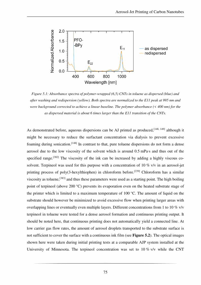
Aerosol-Jet Printing of Carbon Nanotubes
75
As demonstrated before, aqueous dispersions can be AJ printed as produced,[148, 149] although it
might be necessary to reduce the surfactant concentration via dialysis to prevent excessive
foaming during sonication.[148] In contrast to that, pure toluene dispersions do not form a dense
aerosol due to the low viscosity of the solvent which is around 0.5 mPa·s and thus out of the
specified range.[382] The viscosity of the ink can be increased by adding a highly viscous co-
solvent. Terpineol was used for this purpose with a concentration of 10 % v/v in an aerosol-jet
printing process of poly(3-hexylthiophen) in chloroform before.[239] Chloroform has a similar
viscosity as toluene,[383] and thus these parameters were used as a starting point. The high boiling
point of terpineol (above 200 °C) prevents its evaporation even on the heated substrate stage of
the printer which is limited to a maximum temperature of 100 °C. The amount of liquid on the
substrate should however be minimized to avoid excessive flow when printing larger areas with
overlapping lines or eventually even multiple layers. Different concentrations from 1 to 10 % v/v
terpineol in toluene were tested for a dense aerosol formation and continuous printing output. It
should be noted here, that continuous printing does not automatically yield a connected line. At
low carrier gas flow rates, the amount of aerosol droplets transported to the substrate surface is
not sufficient to cover the surface with a continuous ink film (see Figure 5.2). The optical images
shown here were taken during initial printing tests at a comparable AJP system installed at the
University of Minnesota. The terpineol concentration was set to 10 % v/v while the CNT
Figure 5.1: Absorbance spectra of polymer-wrapped (6,5) CNTs in toluene as dispersed (blue) and
after washing and redispersion (yellow). Both spectra are normalized to the E11 peak at 995 nm and
were background corrected to achieve a linear baseline. The polymer absorbance (< 400 nm) for the
as dispersed material is about 6 times larger than the E11 transition of the CNTs.

Aerosol-Jet Printing of Carbon Nanotubes
76
concentration could not be reliably determined at the time. The total flow, i.e. sheath plus carrier
gas, was held constant at 90 sccm.
For actual device manufacturing later, the sheath gas flow was reduced to 30 sccm independent
of the carrier gas flow. The resulting increase in the linewidth from around 25 µm to around 60 µm
is favorable for printing larger areas as it reduces the number of lines necessary to cover a certain
area. During printing, the stage was heated to 100 °C and thus the toluene evaporated rather
quickly. The alignment camera images shown in Figure 5.2 are a result of the terpineol remaining
on the substrate. As evident from the images, already slight variations significantly alter the
appearance of the printing output. While there were still only slightly connected droplets at a
carrier flow of 13 sccm, a continuous line with an approximate linewidth of 25 µm was found at
14 sccm (and a corresponding sheath gas flow of 76 sccm). This line became thicker and wider
for further increased carrier flow which resulted in more liquid remaining on the substrate. The
carrier flow was thus set to the minimum value resulting in continuous film.
Depending on the exact setup, e.g. the position of the pickup tube within the vial, the ink vial
shape and size, and the material, the carrier flow necessary to print a continuous film had to be
determined at the beginning of each printing session, before starting deposition on the actual
samples. While this seems difficult at first, it was observed that the adjustment of only the carrier
gas flow towards a continuous output was sufficient. This process was best done on the reference
silicon chip that was also used for the alignment of nozzle and camera, because of the good
contrast of printed material and substrate visible in both – the alignment and the process –
cameras. Additionally, the range of necessary variation was relatively small and a good output for
toluene/terpineol based CNT inks was usually attained at (14 ± 1) sccm. For some configurations
however, the flow had to be increased to up to 20 sccm to achieve the desired dense deposition
on the substrate.

Aerosol-Jet Printing of Carbon Nanotubes
77
Figure 5.2: Optical images of printing output at different carrier gas flows (left to right: 12 – 13 – 14
– 15 sccm) showing the shift from individual droplets to a complete film filling the printed line. All
micrographs were adjusted for contrast and brightness for better visibility. Scale bars are 20 µm.
While continuous lines could be easily observed and might even be quantified with respect to
thickness and width, the formation of a dense aerosol could only be evaluated by the naked eye
and was thus not completely objective. However, a measurement of the aerosol density, i.e. by
absorbance measurements, was impossible due to reflections at the ink vial and the surrounding
water cooling system whose continuous flow introduced air bubbles and turbulences into the water
stream. It was found, that concentrations from 5 to 10 % v/v terpineol resulted in a seemingly
dense aerosol. A concentration of 5 % v/v was chosen as a good tradeoff between maximized
aerosol density and minimized liquid remaining on the sample surface for all future ink
formulations.
Special attention towards the ink vial should be paid during the evaluation of different solvents
and solvent mixtures or final inks. The bottom of the used ink vials was blown out into a
hemisphere to reduce the glass thickness and remove sharp edges. Differences in the handling by
the glassblower performing this task might lead to slightly different shapes or glass thicknesses
that are not visible to the naked eye. The suitability of all ink vials was thus first validated with
pure deionized water. Almost identical looking vials sometimes gave a very strong aerosol and
other times no aerosol at all. Comparing different solvents or material concentrations should thus
always be performed using a single ink vial. Additionally, the reproducibility of one printing
process with set parameters also relied on an unchanged setup, i.e. also the use of the same ink
vial. If the utilized vial gave a strong aerosol, only slight carrier flow changes had to be performed,
if at all.

Aerosol-Jet Printing of Carbon Nanotubes
78
The second variable parameter is the concentration of the active material, i.e. for this study the
carbon nanotubes. Although the volumes of the dispersions significantly improved by shifting
from bath sonication in small vials (~ 10 mL of dispersion in one batch) towards shear-force
mixing (up to 500 mL), the material availability was still limited. On the other hand, high
concentrations increase the probability of re-aggregation especially due to the low polymer-
content remaining after washing the CNT pellet or filter cake as discussed before (see Figure 5.1).
While excess polymer was used to initially disperse the nanotubes, the insulating polymer should
be removed as much as possible while avoiding aggregates and bundles as they have a negative
influence on the charge transport properties of the CNT network.[45] Ideally only polymer wrapped
around the nanotubes should remain after the redispersion of the washed pellet in fresh toluene.
Therefore, a relatively low CNT concentration is preferred during the material deposition process.
However, if the active material content in the ink is too low, the stage speed has to be decreased
or several layers have to be printed to form percolating networks of carbon nanotubes. Both
options resulted in an increased deposition of terpineol on the substrate (as the toluene is
evaporating almost immediately on the stage heated to 100 °C) which led to a higher flow of
material, thus a larger spread around the desired printing area and a loss in resolution.
Additionally, the processing times were longer especially for the thicker CNT films described
later. While this is not a serious issue on the lab-scale, it would be problematic in roll-to-roll
fabrication processes. One possible solution to tackle the problem of extended printing times
without altering the ink composition would be to multiplex the printing process, i.e. use several
printing heads in series.
For the fabrication of transistors, a homogeneous network density is desired, i.e. the network
should not exhibit any holes or areas with increased bundling. At very low CNT concentrations,
both effects could be observed simultaneously – holes due to the low amount of material deposited
as well as bundling most probably due to drying effects. The morphology of the nanotube network
was determined by AFM imaging. Representative AFM images showing the range of unwanted
printing results, i.e. coverage below the percolation threshold, bundling, and sparse networks,
together with a CNT film printed with improved printing parameters are presented in Figure 5.3.

Aerosol-Jet Printing of Carbon Nanotubes
79
Figure 5.3: AFM images of printed (6,5) CNTs showing very low density, bundling, a sparse network
and a reasonably homogeneous CNT film (left to right). Scale bars are 500 nm.
While sparse networks are not completely unwanted and might be even helpful for some studies,
they tend to be less reproducible and often exhibit completely uncovered areas (see section 5.7).
Continuous and dense networks from a single printing layer could be obtained for an initial CNT
concentration of at least 1.8 mg L−1 in 1 mL initial ink volume placed in the printer vial. This
value corresponds to an optical density of 1.0 at the E11 peak (λ = 995 nm) for a 1 cm long cuvette
and was used for all further experiments if not noted otherwise. Adjustment of concentrations
from the dispersion to the final ink were always based on absorbance measurements to enable a
quick and reliable determination of the CNT concentration.
5.3. Stability of Carbon Nanotube Inks
The desired properties of carbon nanotubes, in particular large length and low defect-density, are
generally reduced by strong sonication as the energy input introduces more defects and breaks the
nanotubes thus reducing the average length.[110, 378, 384] The aerosol-jet process however relies, at
least when not utilizing the more gentle pneumatic atomizer, on sonicating of the ink to push small
droplets from the liquid into the aerosol phase. This raises questions about the suitability of this
process for carbon nanotubes and was hence investigated.
All material used in the following were prepared by applying ultrasonication to debundle the
nanotubes and enable efficient polymer-wrapping during the dispersion process. The mean length
of the nanotubes in the starting material was thus slightly longer than 1 µm after redispersion in
fresh toluene.[110, 385] Both possible effects, shortening and increase of defect density, were
simultaneously studied by printing two different patterns from the same ink after different times
of sonication at maximum power. A dense network was used for Raman analysis to provide

Aerosol-Jet Printing of Carbon Nanotubes
80
sufficient signal for reliable peak fits and sparse individualized nanotubes were necessary for
length determination. Printing individualized CNTs was realized by a pattern of dots instead of
continuous lines, i.e. only depositing very small amounts of material during the short opening
period of the shutter. The CNT lengths were determined from atomic force microscopy images
using a JAVA program written by Andreas Malhofer. Several points along the nanotube were
manually selected and the length of the connecting spline was calculated and saved by the
program. A typical AFM image with only few CNTs is shown in Figure 5.4. The blue lines mark
the manually traced nanotubes chosen for length determination because they were undoubtedly
individual nanotubes and not overlapping or bundled. For each sonication time, more than 50
CNTs were measured and incorporated into the statistical evaluation. The patterns were printed
right after setting up the printer and after 15, 30, and 46 hours of continuous sonication at the
maximum possible atomizer power. The nanotube length obtained from the first sample was in
the expected range of around 1 µm.[110]
For the first 30 h of constant sonication by the atomizer of the AJ printer no significant decrease
in the nanotube length was observed. Other sonication methods frequently used during nanotube
dispersion such as tip sonicating show a significantly larger impact on the nanotube length,
shortening the same material to around 0.6 µm within several hours.[110] Experimental studies
showed a strong influence of the nanotube length on photoluminescence yield an device
performance, especially for rather short (<1 µm) nanotubes.[386] Simulations support these
observations also for longer nanotubes however with a less pronounced impact.[74] In composites
of nanotubes and insulating polymers with a CNT concentration close to the percolation limit,
small changes of around 15 % of the average length can already have a strong influence on the
device performance, i.e. effective mobility or on-current, even for CNTs longer than 1 µm.[385]
The shortening of printed nanotubes observed here, after almost 2 days of constant sonication was
rather small (less than 10 %) and most tubes still exhibited a length of around 1 µm or above. The
influence on the device performance of nanotube network transistors should thus be rather small,
especially as the tested sonication times exceeded the usual processing times by at least one order
of magnitude.

Aerosol-Jet Printing of Carbon Nanotubes
81
Figure 5.4: Left: Typical AFM image for length determination of printed nanotubes showing manually
inserted measurement splines (blue). The scale bar is 500 nm. The statistical evaluation of CNT length
versus sonication time (right) shows almost no decrease in length.
The second question regarding negative influences of sonication concerns the defect density along
the CNTs. After the same sonication times as for the AFM length analysis, squares of dense
networks were printed as well. Theses squares were mapped via Raman spectroscopy to evaluate
the amount of defects in the CNTs after printing. The representative Raman spectrum in
Figure 5.5 shows the barely visible radial breathing mode (RBM), the peak of the silicon
substrate, small D and G− bands, as well as large signals for the G+ and 2D bands. According to
literature, the ratio of the G+ band and the 2D band increases with defect density and is thus a
good figure-of-merit.[387] For quantification of the G+ to 2D ratio, the Raman spectra of the printed
dense films were mapped under resonant excitation with a 532 nm laser and both relevant peaks
were fitted using the Renishaw Raman software Wire 3.4. The statistical analysis shows almost
no change within the first 15 hours of continuous sonication. Only after this already long
sonication period, a significant increase of the G+/2D-ratio and thus a decrease in nanotube quality
was observed. It should be noted that the long sonication times of the same ink were realized by
overnight sonication without any output, i.e. carrier and sheath gas flow rates were set to zero.
The gas flows were increased only during deposition for sample preparation. In contrast to that,
the usual processing times of 1 mL ink volume were less than 5 hours when printing multiple
samples with interruptions – thus no output – for the alignment of the samples and maybe
additional processing steps. If an uninterrupted aerosol output is used for continuous device

Aerosol-Jet Printing of Carbon Nanotubes
82
fabrication, the ink is consumed completely even faster. It can thus be concluded from the length
and defect analysis that within the timeframe of typical printing processes no negative influence
of the continuous sonication necessary to create the aerosol occurs.
Figure 5.5: Raman spectrum of (6,5) CNTs and statistical evaluation of the G+/2D-ratio versus
sonication time.
Another important factor is the composition of the aerosol for reproducible output results over
extended periods. The first hint is the concentration of nanotubes of the ink remaining in the vial.
While literature often reports an increase in the concentration of solid components in the
remaining liquid, the opposite trend was observed for aerosol-jet printing of carbon nanotubes.
The increasing concentration reported in literature is mostly attributed to the evaporation of
solvent.[388-390] However, these studies on aerosol processes focused on medical applications
where different aerosolizers were used and to the best of my knowledge, there has been no study
on aerosol-jet printing processes dealing with the ink composition over time. Here, the absorbance
of the ink in the vial was measured after consecutive 150 mm of printed path length and showed
a decrease of around 80 % over a total of 600 mm long path (see Figure 5.6). During this process
around 300 µL of ink were consumed from an initial starting volume of 1 mL at an initial
concentration of 1.8 mg L−1. While maintaining all other process parameters constant, reducing
the concentration to 0.3 mg L−1 resulted in an increase of the ink volume consumed for the same
printing path by a factor of 1.5 to 2.

Aerosol-Jet Printing of Carbon Nanotubes
83
Figure 5.6: Absorbance spectra of CNT ink remaining in the ink vial measured after printing different
CNT path lengths.
The aerosolization process strongly depends on the density, surface tension, and viscosity of the
ink as well as the input of ultrasonic power.[391] This means, that the (local) ink composition and
the filling level of the vial can have a strong influence on the aerosol droplet formation. As the
viscosity of CNT dispersions increases with CNT concentration and length,[392-394] CNT-rich
droplets might be aerosolized preferentially and thereby reduce the CNT concentration in the
remaining ink. A simpler reason for the reduction of CNT concentration was the observed
deposition of CNTs on the upper parts of the ink vial where the aerosol was still present in the
vial but well above the liquid filling level. While the solvent ran down the side of the vial, CNTs
remained on the vial wall. This deposition was almost impossible to observe after just a few
printing runs even over extended times as the CNTs are not visible for the naked eye unless they
form relatively thick films of more than 30 nm. Ink vials re-used for the same CNT material and
thus not thoroughly cleaned after each ink were showing the typical blue-purple color of (6,5)
nanotubes after a large amount of sample sets produced for different projects as shown in
Figure 5.7.

Aerosol-Jet Printing of Carbon Nanotubes
84
Figure 5.7: Photograph of ink vials fresh (left) and after printing (6,5) nanotubes for several projects
(right) illustrating the material deposition in the upper part of the vial. The photographs were adjusted
for brightness and contrast to increase visibility.
Even more important than the composition of the ink remaining in the vial was the actual output
printed on the substrate. One indicator for constant or varying output were the device
characteristics of the final FET that will be discussed in section 5.4. Additionally, the output could
be quantified by Raman mapping at least to some degree using the G+ band intensity. Squares of
500x500 µm2 were printed for that purpose from inks with different CNT concentrations of 0.2 to
1.8 mg L−1 and two different initial ink volumes (1.0 and 0.4 mL). As shown in Figure 5.8, the
output indeed varied significantly and decreased with both, CNT concentration and initial ink
volume. At half of the usually used concentration, i.e. 0.9 mg L−1, the output decreased to 46 %
and 40 % of the initial value for V = 1.0 mL and V = 0.4 mL, respectively. As expected, the output
was further reduced for lower CNT concentrations, however, at very low concentrations of 0.2
and 0.4 mg L−1, the obtained values were very similar. It was not thus possible to extract a linear
relation between output and ink composition within the measured range.

Aerosol-Jet Printing of Carbon Nanotubes
85
Figure 5.8: G+-band intensity normalized to the silicon peak intensity at 520 cm−1 of squares printed
on silicon substrates from inks with different initial ink volumes (top: 1.0 mL, bottom: 0.4 mL) and
CNT concentration (left to right: 1.8, 0.9, 0.4, and 0.2 mg L−1) acquired by Raman mapping. The
average values including the standard deviation are given next to the individual images.
The hot spots with high signals might be explained by drying effects while at higher
concentrations slight bundling might play an additional role. The 5x5 µm2 AFM images, recorded
in the middle of the printed area, however do not show increased bundling but a CNT film with
variations in the local density for inks with higher concentrations (see Figure 5.9). The images at
lower concentrations show large areas completely uncovered and only small spots with nanotubes.
It should be noted that squares with a line pitch of 25 µm were printed on silicon chips to enable
a better Raman evaluation by facilitating the normalization to the silicon peak at 520 cm−1. Since
the transistors were eventually fabricated on glass substrates with pre-patterned gold electrodes,
the situation may be different within the actual FET channels due to the substrate profile with
steep steps at the electrode edges and different surface properties.

Aerosol-Jet Printing of Carbon Nanotubes
86
Figure 5.9: AFM images taken in the middle of the printed squares printed on silicon from inks with
different initial ink volumes (top: 1.0 mL, bottom: 0.4 mL) and CNT concentrations (left to right: 1.8,
0.9, 0.4, and 0.2 mg L−1). Scale bars are 1 µm.
The Raman intensity was thus mapped directly on the 1st and last, i.e. 128th, transistor printed
from the same ink (see Figure 5.10). Here, a decrease by only around 33 % was observed in the
Raman intensity while the CNT concentration in the ink vial decreased by about 80 % while
printing these transistors. As visible in the AFM images, a percolating network was still observed
at a CNT concentration decreased by 50 % and the reduced output may not have a high impact on
the FETs. The influence of the variable output on device parameters such as on-current and on/off-
ratio will be discussed in the next chapter.
Figure 5.10: Decrease of Raman intensity, i.e. amount of CNTs deposited, from the 1st FET (left) and
last, i.e. 128th FET, all printed consecutively from one ink. The total Raman intensity count of the
displayed area is given above the Raman maps.

Aerosol-Jet Printing of Carbon Nanotubes
87
5.4. Reproducibility of Transistor Characteristics
The possibility to move from lab scale device fabrication of a few FETs towards application of
these devices in circuits that require more than one working transistor crucially depends on the
reproducibility of the device characteristics. This reproducibility not only refers to the similarity
of devices produced from one ink but also batch-to-batch variations given that the same process
parameters are used. Although the ultimate goal of printed electronics is all-printed devices, the
focus here is on the semiconducting layer, i.e. the CNTs, and therefore a well-established device
architecture was utilized (see Figure 5.11). Interdigitated source and drain electrodes were
patterned by standard photolithography on glass substrates. A positive double-layer resist was
exposed to the i-line of a mercury lamp through a chrome-on-glass mask followed by development
in a static bath. After electron-beam evaporation of chromium (2 nm) as adhesion layer and gold
(30 nm), the subsequent lift-off in NMP finalized the electrode structure. Each substrate
compromised the source and drain electrodes of 4 transistors of each channel length L, i.e. 5, 10,
20, and 40 µm, with a channel width of 10 mm for all L but 40 µm, where the channel width was
5 mm. Aerosol-jet printing was performed from a CNT ink with a concentration of 1.8 mg L−1 by
printing a single line in the middle of each 5 and 40 µm channel. The 10 and 20 µm channels were
only partially printed for the sake of material conservation. For evaluating the reproducibility of
the FETs thus the two extremes, rather short (5 µm) and rather long (40 µm) channels, were used.
Printing in the middle of each channel resulted in different network densities for the different
channel lengths as the pitch, resulting from electrode width plus channel length, was 25 µm for
L = 5 µm and 60 µm for L = 40 µm. A direct comparison between the different channel lengths
was thus not possible for these devices. The linewidth for the employed stage speed (0.5 mm s−1),
sheath (30 sccm) and carrier (14 ± 1 sccm) flows, was around 60 µm and resulted in a continuous
film across the whole device area for both pitches. The stage temperature of 100 °C promoted fast
toluene evaporation and thereby reduced flow on the substrate. The remaining terpineol and
potentially present excess polymer were removed by a rinsing step with THF and de-ionized water
followed by drying with a nitrogen gun.
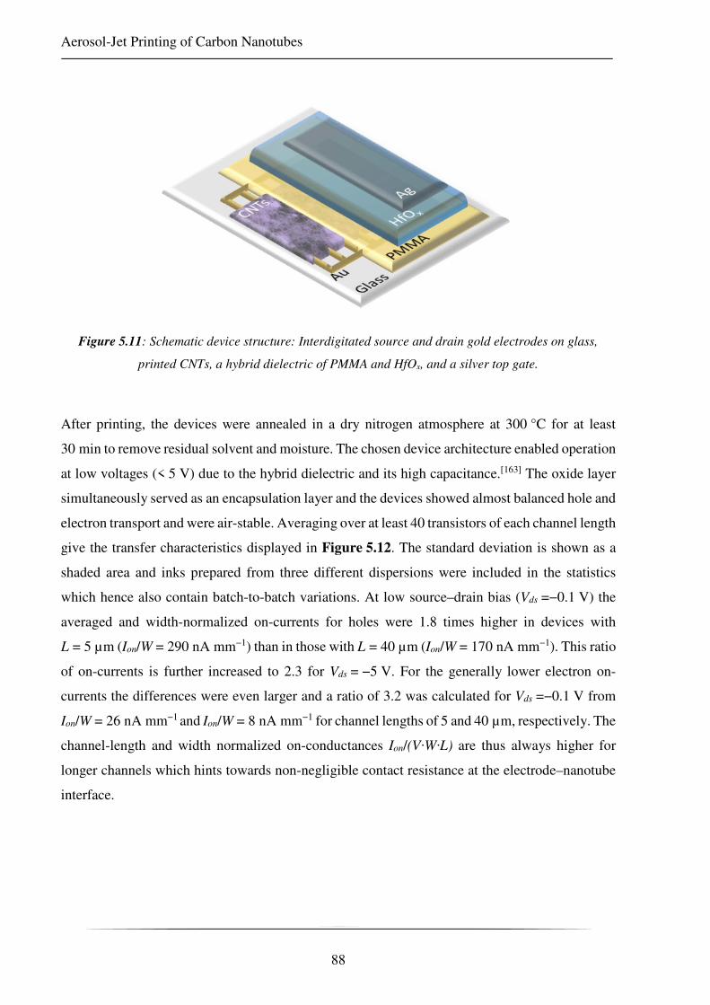
Aerosol-Jet Printing of Carbon Nanotubes
88
Figure 5.11: Schematic device structure: Interdigitated source and drain gold electrodes on glass,
printed CNTs, a hybrid dielectric of PMMA and HfOx, and a silver top gate.
After printing, the devices were annealed in a dry nitrogen atmosphere at 300 °C for at least
30 min to remove residual solvent and moisture. The chosen device architecture enabled operation
at low voltages (< 5 V) due to the hybrid dielectric and its high capacitance.[163] The oxide layer
simultaneously served as an encapsulation layer and the devices showed almost balanced hole and
electron transport and were air-stable. Averaging over at least 40 transistors of each channel length
give the transfer characteristics displayed in Figure 5.12. The standard deviation is shown as a
shaded area and inks prepared from three different dispersions were included in the statistics
which hence also contain batch-to-batch variations. At low source–drain bias (Vds =−0.1 V) the
averaged and width-normalized on-currents for holes were 1.8 times higher in devices with
L = 5 µm (Ion/W = 290 nA mm−1) than in those with L = 40 µm (Ion/W = 170 nA mm−1). This ratio
of on-currents is further increased to 2.3 for Vds = −5 V. For the generally lower electron on-
currents the differences were even larger and a ratio of 3.2 was calculated for Vds =−0.1 V from
Ion/W = 26 nA mm−1 and Ion/W = 8 nA mm−1 for channel lengths of 5 and 40 µm, respectively. The
channel-length and width normalized on-conductances Ion/(V·W·L) are thus always higher for
longer channels which hints towards non-negligible contact resistance at the electrode–nanotube
interface.
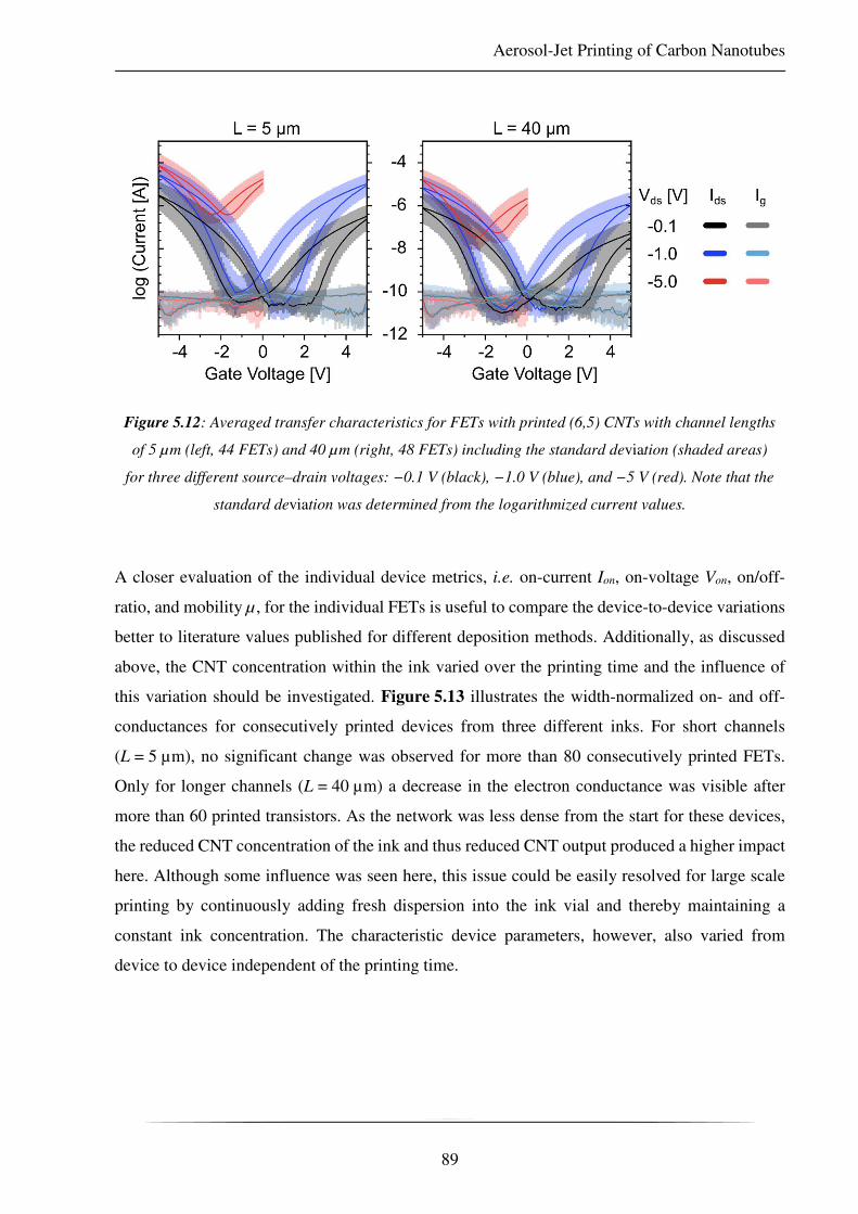
Aerosol-Jet Printing of Carbon Nanotubes
89
Figure 5.12: Averaged transfer characteristics for FETs with printed (6,5) CNTs with channel lengths
of 5 µm (left, 44 FETs) and 40 µm (right, 48 FETs) including the standard deviation (shaded areas)
for three different source–drain voltages: −0.1 V (black), −1.0 V (blue), and −5 V (red). Note that the
standard deviation was determined from the logarithmized current values.
A closer evaluation of the individual device metrics, i.e. on-current Ion, on-voltage Von, on/off-
ratio, and mobility µ , for the individual FETs is useful to compare the device-to-device variations
better to literature values published for different deposition methods. Additionally, as discussed
above, the CNT concentration within the ink varied over the printing time and the influence of
this variation should be investigated. Figure 5.13 illustrates the width-normalized on- and off-
conductances for consecutively printed devices from three different inks. For short channels
(L = 5 µm), no significant change was observed for more than 80 consecutively printed FETs.
Only for longer channels (L = 40 µm) a decrease in the electron conductance was visible after
more than 60 printed transistors. As the network was less dense from the start for these devices,
the reduced CNT concentration of the ink and thus reduced CNT output produced a higher impact
here. Although some influence was seen here, this issue could be easily resolved for large scale
printing by continuously adding fresh dispersion into the ink vial and thereby maintaining a
constant ink concentration. The characteristic device parameters, however, also varied from
device to device independent of the printing time.

Aerosol-Jet Printing of Carbon Nanotubes
90
Figure 5.13: On- (at Vg = −5 V) and off-conductances for Vds = −1 V versus total number of
transistors with printed (6,5) CNTs. Three separately prepared inks are shown for two channel lengths
(left: 5 µm and right: 40 µm). The total printed path length of 100 samples is more than 900 mm.
The turn-on voltages for a source–drain bias of −0.1 V were between −1.5 V to +1.5 V for more
than 90 % of the measured transistors. The distribution of device parameters is shown in the bar
graphs in Figure 5.14. On average, FETs with a channel length of 40 µm turned on at a gate
voltage of (1.0 ± 0.8) V and (−0.5 ± 0.7) V for electrons and holes, respectively. Even smaller
average values for Von – although with a similar spread – could be extracted for the devices with
a denser network of CNTs at a channel length of 5 µm with (0.7 ± 1.1) V and (−0.4 ± 1.0) V for
electrons and holes, respectively. These and the following average values include all outliers. The
turn-on voltage was determined from the transfer characteristics at the point where – coming from
the off-state – the source–drain current consistently became larger than the gate leakage.
As already seen in the averaged transfer characteristics and as expected for a random carbon
nanotube network, the width-normalized on-conductances extracted at Vds = −1 V were higher for
the shorter channel length with higher CNT density: (4.4 ± 3.6) vs (2.0 ± 1.6) µS mm−1 for holes
and (1.5 ± 2.2) vs (0.4 # 0.4) µS mm−1 for electrons. The different channel widths (W = 5 mm for
L = 40 µm and W = 10 mm for L = 5 µm) lead to even larger differences in the on-currents. In
short channels the on-currents reached (44 ± 36) µA for holes and (15 ± 22) µA for electrons
while in long channels Ion was about 4 to 8 times lower: (10 ± 8) µA for holes and (2 ± 2) µA for
electrons.

Aerosol-Jet Printing of Carbon Nanotubes
91
Table 5.1: Overview of device parameters extracted from FETs with AJ printed (6,5) CNTs.
L = 5 µm L = 40 µm
Parameter h+ e- h+ e-
Turn-on voltage [V] −0.4 ± 1.0 0.7 ± 1.1 −0.5 ± 0.7 1.0 ± 0.8
On-conductance [µS mm−1] 4.4 ± 3.6 1.5 ± 2.2 2.0 ± 1.6 0.4 # 0.4
On-current [µA] 44 ± 36 15 ± 22 10 ± 8 2 ± 2
Log (on/off-ratio) 6.4 ± 1.2 6.0 ± 1.2 6.6 ± 0.6 5.8 ± 0.6
Mobility [cm2 V−1 s−1] 0.34 ± 0.11 0.03 ± 0.03 1.90 ± 1.17 0.11 ± 0.11

Aerosol-Jet Printing of Carbon Nanotubes
92
Figure 5.14: Statistical evaluation of device characteristics for L = 5 µm (left column) and L = 40 µm
(right column): Turn-on-voltage (top) extracted at Vds =−0.1 V, on-current (middle) and on/off-ratio,
both extracted at Vds = −1.0 V.

Aerosol-Jet Printing of Carbon Nanotubes
93
The variations in currents, turn-on voltage and on-off ratio might raise the question if this
variability is sufficient for applications. However, most publications showing more than a few
FETs and reporting device-to-device variations for CNT transistors state similar distributions for
printed nanotube layers.[221, 265] Alternative deposition methods such as spin-coating,[168] dip-
coating,[368] or simple immersion,[147, 369, 395, 396] also do not show a much higher uniformity. With
such FETs and their associated spread of device characteristics presented in literature it was still
possible to fabricate simple logic gates.[396] Furthermore, even integrated circuits,[368] static
random access memories,[397] and active matrix backplanes for tactile sensors,[369] were reported.
The here obtained device variations should thus be sufficiently small to enable the use of FETs in
circuitry and more complex applications.
The high purity of the polymer-wrapped large bandgap (6,5) nanotubes and especially the absence
of metallic species resulted in very low off-currents which were basically only limited by the gate
leakage. As the hybrid dielectric also enabled low gate leakages (≲1 nA) as demonstrated
before,[33, 163] high on/off-ratios of 106−107 could be reached for low source–drain voltages
(Vds = −1 V). Due to the lower on-currents of the 40 µm long channels, these devices exhibit
slightly lower on/off-ratios. As the probability of percolating paths by residual metallic CNTs
decreases with the channel length, lower on/off-ratios (in the order of 104) due to increased off-
currents were found less often among those devices as well. For the best FETs with L = 5 µm
on/off-ratios of up to 1.8·108 for holes and 6.1·107 for electrons were reached at a source–drain
bias of ± 3 V (see Figure 5.15), thus exceeding values reported in the existing literature.[1, 146]
Further reduction of the gate leakage was achieved by measuring with triaxial instead of the
usually used coaxial cables and thus reduced noise levels of the measurement setup. The off-
current was thus limited by the drain current minimum point of the transfer curve, which was
slightly above the gate leakage. The V-shape of the transfer characteristic results from the
ambipolar behavior, i.e. the simultaneous transport of holes and electrons (compare chapter 2.2.6),
that becomes apparent at elevated Vds. For larger Vds, the off-currents of the devices increase and
thus reduce the on/off-ratio again as evident from the averaged transfer characteristics shown in
Figure 5.12. For smaller bandgap nanotubes the increase of the off-current already starts at much
lower source–drain bias due to the lower turn-on voltages.[52] The large bandgap and comparably
large turn-on voltages of (6,5) CNTs thus support reaching higher on/off-ratios. Ambipolar
transport is often unfavorable in applications not only because of the limitations concerning
on/off-ratios but also in integrated, complimentary circuits where it results in increased power
dissipation. This problem could be addressed by p- or n-doping of the nanotube network and thus

Aerosol-Jet Printing of Carbon Nanotubes
94
unipolar transport. A successful attempt of completely suppressing hole transport was recently
demonstrated by doping (6,5) CNTs with a guanidino-functionalized aromatic compound. With
the same device architecture as used here, Schneider et al. demonstrated the complete absence of
hole transport even at high Vds of up to −5 V and reached on/off-ratios for electrons of up to
2·108.[144]
Figure 5.15: Best on/off-ratios achieved with an FET with of AJ printed (6,5) CNTs with L = 5 µm:
1.8·108 for holes at Vds = −3 V and 6.1·107 for electrons at Vds = +3 V.
For the AJ printed FETs, higher channel length normalized currents for longer channels and thus
also higher apparent device mobilities were extracted. The linear field-effect mobilities for holes
were (0.34 ± 0.21) and (1.90 ± 1.17) cm2 V−1 s−1 for 5 and 40 µm long channels, respectively.
They were calculated using standard transistor equations within the gradual channel
approximation and with the capacitance measured directly at the channel. The electron mobilities
were about one order of magnitude lower with (0.03 ± 0.03) and (0.11 ± 0.11) cm2 V−1 s−1.
Figure 5.16 shows that there is no systematic decrease of the hole mobility with the number of
printed transistors from one ink but rather a device-to-device variation. It further demonstrates a
large dependence of the mobilities on the channel length that can be mainly explained by contact
resistance. A decrease of the apparent device mobility by a factor of 3 to 4 was even demonstrated
for large diameter (and thus small bandgap) nanotubes and different channel lengths.[52] For the
here employed large bandgap CNTs, this effect is expected to be even more pronounced.[41, 398]
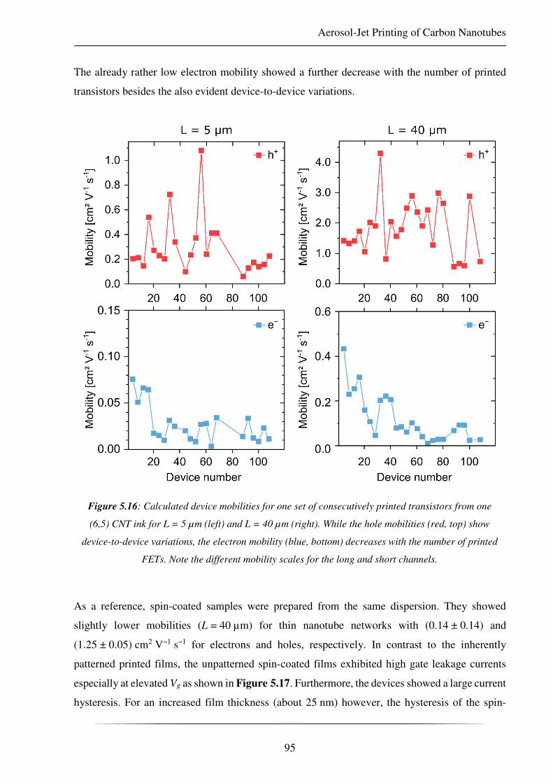
Aerosol-Jet Printing of Carbon Nanotubes
95
The already rather low electron mobility showed a further decrease with the number of printed
transistors besides the also evident device-to-device variations.
Figure 5.16: Calculated device mobilities for one set of consecutively printed transistors from one
(6,5) CNT ink for L = 5 µm (left) and L = 40 µm (right). While the hole mobilities (red, top) show
device-to-device variations, the electron mobility (blue, bottom) decreases with the number of printed
FETs. Note the different mobility scales for the long and short channels.
As a reference, spin-coated samples were prepared from the same dispersion. They showed
slightly lower mobilities (L = 40 µm) for thin nanotube networks with (0.14 ± 0.14) and
(1.25 ± 0.05) cm2 V−1 s−1 for electrons and holes, respectively. In contrast to the inherently
patterned printed films, the unpatterned spin-coated films exhibited high gate leakage currents
especially at elevated Vg as shown in Figure 5.17. Furthermore, the devices showed a large current
hysteresis. For an increased film thickness (about 25 nm) however, the hysteresis of the spin-
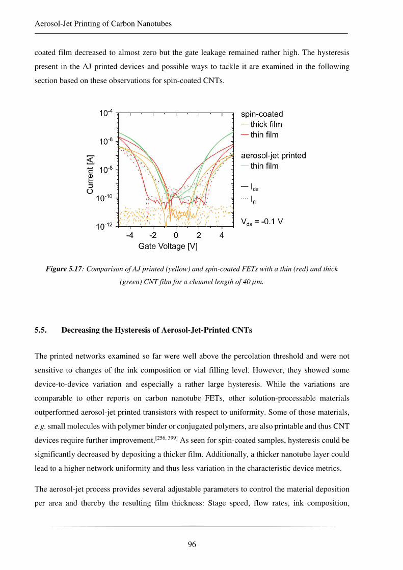
Aerosol-Jet Printing of Carbon Nanotubes
96
coated film decreased to almost zero but the gate leakage remained rather high. The hysteresis
present in the AJ printed devices and possible ways to tackle it are examined in the following
section based on these observations for spin-coated CNTs.
Figure 5.17: Comparison of AJ printed (yellow) and spin-coated FETs with a thin (red) and thick
(green) CNT film for a channel length of 40 µm.
5.5. Decreasing the Hysteresis of Aerosol-Jet-Printed CNTs
The printed networks examined so far were well above the percolation threshold and were not
sensitive to changes of the ink composition or vial filling level. However, they showed some
device-to-device variation and especially a rather large hysteresis. While the variations are
comparable to other reports on carbon nanotube FETs, other solution-processable materials
outperformed aerosol-jet printed transistors with respect to uniformity. Some of those materials,
e.g. small molecules with polymer binder or conjugated polymers, are also printable and thus CNT
devices require further improvement.[256, 399] As seen for spin-coated samples, hysteresis could be
significantly decreased by depositing a thicker film. Additionally, a thicker nanotube layer could
lead to a higher network uniformity and thus less variation in the characteristic device metrics.
The aerosol-jet process provides several adjustable parameters to control the material deposition
per area and thereby the resulting film thickness: Stage speed, flow rates, ink composition,

Aerosol-Jet Printing of Carbon Nanotubes
97
printing pattern, and printing of multiple layers. The least labor-intensive change would be the
decrease of the stage speed or increase of the carrier flow rate. For both cases, only one parameter
would have to be altered before the material deposition. However, both lead to more aerosol
droplet deposition per area and thus also more solvent deposition. While the main solvent toluene
evaporates rather quickly, the high boiling point co-solvent terpineol (TB = 213–218 °C) that is
necessary for proper aerosol formation would accumulate on the substrate. As the stage heating
is limited to a temperature of 100 °C, also toluene remains for some time on the substrate before
evaporating, especially when changing the deposition location only very slowly. This would lead
to a solvent film on the sample surface and thus an increased flow of material on the substrate.
This might lead to less uniformity and a larger overall deposition area of the CNTs. The resulting
lower spatial resolution would eventually reduce the packing density of the FETs on the substrate
and lead to severe device cross-talk. The increased material consumption, limited controllability,
and loss in patterning accuracy exclude these simple approaches for increasing the thickness of
the deposited film.
When changing the ink composition all other parameters could in principle remain constant, only
the carrier gas flow may have to be adjusted. Increasing the CNT content is only possible up to a
certain limit, as for too high concentrations two negative effects can occur. The dispersion can
become less stable and thus more bundling takes place which is unfavorable for efficient charge
transport.[44, 45] Additionally, a high solids content in the aerosol leads to faster clogging of the
200 µm inner diameter nozzle of the printer.
A change of the printing pattern, e.g. reducing the pitch between adjacent lines, might induce
similar problems as reducing the stage speed or increasing the flow. However, the pattern can be
designed so that adjacent lines are not directly printed one after the other. Instead, every second
line could be printed in the first cycle and the remaining lines in a second cycle. Thereby, the
deposited material has some time to dry before more material is deposited next to it. Printing
several layers on top of each other relies on the premise that nanotubes are not washed away by
the next printed layer. This has already been shown for spin-coating where consecutive spin steps
are used to increase the density of CNT films.[121, 400] Likewise, no removal of previously
deposited nanotubes was observed for printing of several layers. A reduction of the amount of
solvent remaining on the sample from the previous printing step can be realized by rinsing with
THF and IPA or deionized water and subsequent drying with a nitrogen gun. The rinsing step also

Aerosol-Jet Printing of Carbon Nanotubes
98
reduces the amount of excess wrapping-polymer in each layer and not only at the surface of the
film which would be the case if performed only at the end of printing.
The effect of the described techniques on the device characteristics and hysteresis in particular
was tested by printing on pre-patterned electrodes with a 40 µm channel. The lowest CNT
coverage was realized with a CNT concentration of 2.2 mg L−1 and a printing pitch of 60 µm
between adjacent lines, i.e. one line in the center of each channel. As the lines were 60 µm wide
this led to a complete coverage of the printing area. For a second set of samples, the pitch between
two lines was then decreased by a factor of 2.4 to 25 µm while keeping the ink concentration
constant. A third sample set was fabricated by printing with a 60 µm pitch and a 3 times increased
ink concentration (6.6 mg L−1). Figure 5.18 shows representative transfer characteristics for
devices with all three printing parameter sets. The hysteresis was quantified by the difference
between the turn-on voltage of the forward and reverse sweep ∆Von and depicted in the bar graph.
The mean values with standard deviations as error bars clearly indicate the positive effect of a
thicker nanotube layer as the hysteresis was decreased by a factor of 2 to 3 for both methods. As
expected, the 3-fold increased ink concentration gave slightly better results than the 2.4-fold
decreased pitch as more material was deposited per area.[401] Besides the decreased hysteresis, a
significant increase in apparent device mobilities could be observed. Mobility values of 0.58 and
6.43 cm2 V−1 s−1 were obtained for electrons and holes, respectively.
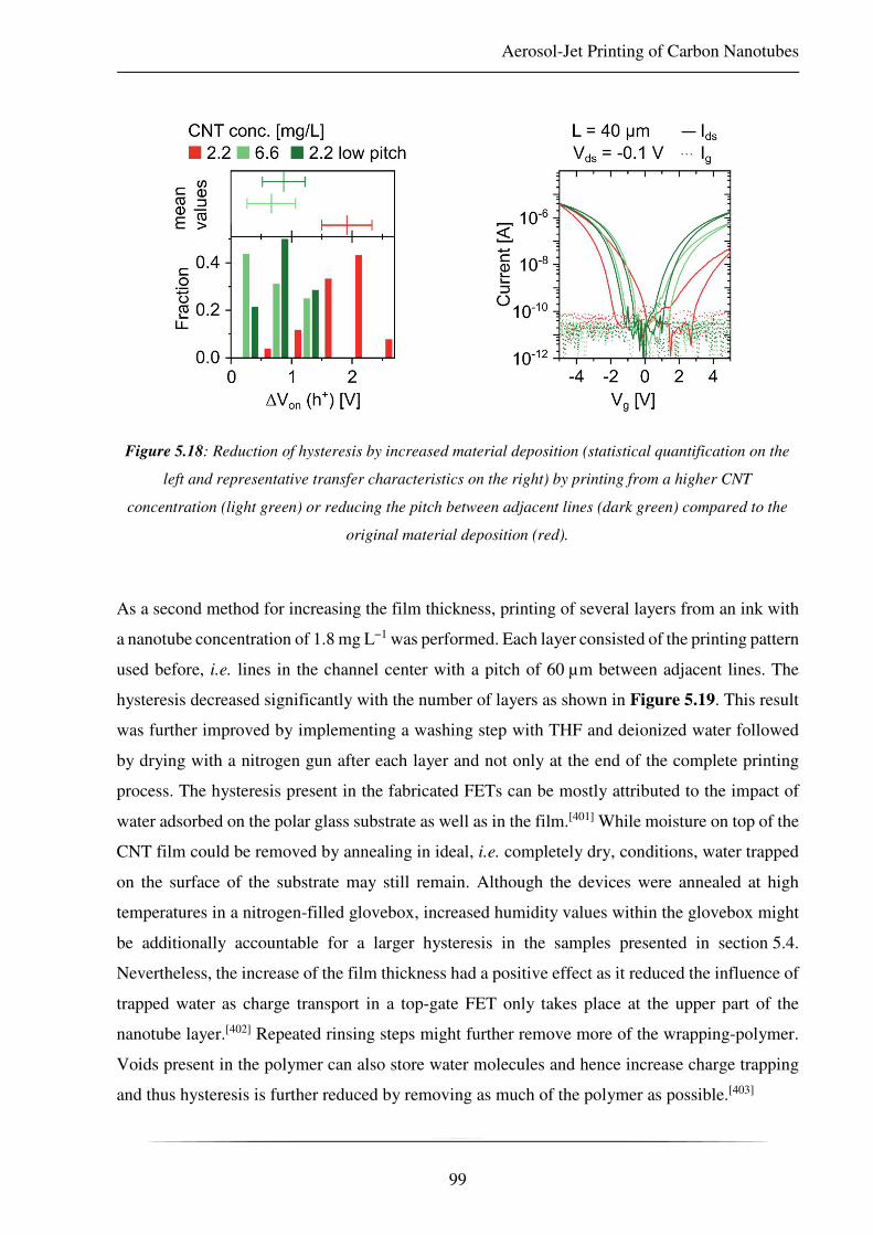
Aerosol-Jet Printing of Carbon Nanotubes
99
Figure 5.18: Reduction of hysteresis by increased material deposition (statistical quantification on the
left and representative transfer characteristics on the right) by printing from a higher CNT
concentration (light green) or reducing the pitch between adjacent lines (dark green) compared to the
original material deposition (red).
As a second method for increasing the film thickness, printing of several layers from an ink with
a nanotube concentration of 1.8 mg L−1 was performed. Each layer consisted of the printing pattern
used before, i.e. lines in the channel center with a pitch of 60 µm between adjacent lines. The
hysteresis decreased significantly with the number of layers as shown in Figure 5.19. This result
was further improved by implementing a washing step with THF and deionized water followed
by drying with a nitrogen gun after each layer and not only at the end of the complete printing
process. The hysteresis present in the fabricated FETs can be mostly attributed to the impact of
water adsorbed on the polar glass substrate as well as in the film.[401] While moisture on top of the
CNT film could be removed by annealing in ideal, i.e. completely dry, conditions, water trapped
on the surface of the substrate may still remain. Although the devices were annealed at high
temperatures in a nitrogen-filled glovebox, increased humidity values within the glovebox might
be additionally accountable for a larger hysteresis in the samples presented in section 5.4.
Nevertheless, the increase of the film thickness had a positive effect as it reduced the influence of
trapped water as charge transport in a top-gate FET only takes place at the upper part of the
nanotube layer.[402] Repeated rinsing steps might further remove more of the wrapping-polymer.
Voids present in the polymer can also store water molecules and hence increase charge trapping
and thus hysteresis is further reduced by removing as much of the polymer as possible.[403]

Aerosol-Jet Printing of Carbon Nanotubes
100
Figure 5.19: Reduction of hysteresis by depositing multiple layers of CNTs: Quantification via the
reduction in the difference between the turn-on voltages in forward and reverse sweep ∆Von (left) for
both, holes (red) and electrons (blue). Rinsing after each deposited layer (open symbols) instead of
rinsing only after printing all layers (solid symbols) further reduces the hysteresis. Representative
transfer characteristics for 1 to 4 printed layers are shown on the right.
Even thicker and eventually optically dense nanotube films could be created by aerosol-jet
printing of multiple layers from inks with higher concentration or by increasing the total number
of layers. Printing 4 consecutive layers from an ink with a concentration of 6.3 mg L−1 resulted in
about 30 nm thick films that are easily visible to the naked eye (see photograph in Figure 5.20).
Absorbance spectra show an optical density of 0.5 of the film at the E11 peak of the (6,5) CNTs.
According to the ink absorbance, the absorption cross section,[404] and the ink consumption, the
transistors presented in section 5.4 required around 40 ng mm−2 of nanotubes. Here, the thick
films required still less than 600 ng mm−2. Alternative deposition methods for thick films are at a
disadvantage here. Spin-coating of films with a thickness of several tens of nanometers is possible
by multiple steps only, and a very high material consumption is inevitable.[405] A large fraction of
the material consumed during spin-coating flies off the spinning substrate. Vacuum filtration or
drop-casting of highly concentrated dispersions on the other hand either need subsequent transfer
steps or lead to very inhomogeneous films.[406-409] While direct patterning is possible by printing,
the deposited material has to be patterned in further processing steps such as photolithography-
assisted plasma etching for other methods to create thick CNT film. This may lead to the

Aerosol-Jet Printing of Carbon Nanotubes
101
introduction of further impurities, e.g. by residual photoresist, and defects especially at the edges
of the patterned area.
Transistors fabricated from aerosol-jet printed thick films showed a negligible hysteresis and
on/off-ratios of more than 106 for L = 5 µm at Vds =−0.1 mV. For a channel length of 40 µm, an
on-conductance of 17 µS mm−1 was observed while the mobilities were 0.7 and 2.8 cm2 V−1 s−1
for electrons and holes, respectively. Channels with L = 5 µm and doubled width exhibited an on-
current increase by one order of magnitude while the off-current was slightly elevated above the
gate leakage. The on/off-ratio was however still larger than 106. Compared to the FETs with only
slightly increased layer thickness presented before, the hole mobility decreased by a factor of 2.3
while the electron mobility was almost constant. This reduction can be attributed to the necessary
vertical charge transport through the semiconducting layer, requiring hopping over many
nanotube junctions. For optimized charge transport the thickness has to be chosen in an optimized
range where trapping by adsorbed water is reduced but vertical transport through the
semiconductor is minimized. In addition, a high density of the network and repeated rinsing steps
to maximize the removal of polymer are favorable.
Figure 5.20: Photograph of a printed CNT films visible to the naked eye (left) and transfer
characteristics of FETs fabricated from such thick films for two channel lengths. Scale bar in the left
image is 5 mm, the film is surrounded by alignment markers printed with Ag ink.

Aerosol-Jet Printing of Carbon Nanotubes
102
5.6. Applications of Printed CNT Films
In this section, some examples of applications of aerosol-jet printed (6,5) CNTs based on the
introduced and optimized procedures described here will be very briefly presented.
Berger et al. used very thick, optically dense (6,5) CNTs for electrochromic notch filters.[111] Film
thicknesses of 10 to 360 nm were prepared by printing multiple layers of an orthogonal grid (line
pitch 25 µm) onto glass with spray-deposited mixed CNT electrodes. In combination with an ion-
gel the CNT layer could be tuned from an optical density of 4.5 at the E11 peak (997 nm) to 0.2
by electrochemical doping.
Held et al. used printed (6,5) nanotubes in combination with dense films of mixed CNTs and an
ion-gel for low-voltage all-carbon semi-transparent transistors.[3] These devices might be
applicable for flexible or even stretchable electronics. Although the device characteristics of
reference samples with gold electrodes were superior due to the high sheet resistance of the
nanotube contacts, the device performance was still good.
Zakharko et al. used a 40–50 nm thick layer of AJ-printed (6,5) CNTs for the investigation of
plexciton propagation in plasmonic crystals.[410] Choosing printing as the deposition method
enabled homogeneous layers with a rather controlled thickness. Furthermore, the nanotubes could
be directly printed onto the pre-patterned array of plasmonic particles without the need of post-
structuring.
Brohmann et al. expanded the printing process from solely (6,5) nanotubes to mixtures of different
CNT chiralities prepared by polymer-wrapping of different CNT sources with different wrapping-
polymers.[44] With the printed networks of nanotubes they then studied temperature-dependent
charge transport to further investigate the transport mechanism.
The range of different successful applications of aerosol-jet printed CNT networks shows the
potential of this method to fabricate reproducible devices with a low material consumption for
electronic and optical applications. Although the patterning accuracy was not optimized, it was
already sufficient for most applications where simply continuous areas of CNTs were needed and
only some precise measurements such as the temperature-dependence study required more
detailed structuring performed on the printed films via photolithography.[44] However, there are
also limitations that will be discussed in the next section.

Aerosol-Jet Printing of Carbon Nanotubes
103
5.7. Limitations of Aerosol-Jet Printing for CNTs
After printing thin but dense networks, the creation of a CNT film with a controlled low density
was attempted. For this, the established ink with polymer-wrapped (6,5) nanotubes was used at a
concentration of 1.8 mg L−1 in toluene with 5 % terpineol. As discussed before, the thickness of
printed CNT films can be controlled by the printing speed. While decreasing the speed to achieve
thicker layers is problematic because of the increased solvent deposition, this problem does not
occur when increasing the stage speed. At constant sheath and carrier flows of 30 and 18 sccm,
respectively, the stage speed v was varied from 0.5 to 2.0 mm s−1. The rather low CNT
concentration led to a full coverage but thin CNT film as shown above. Accordingly, in
combination with a higher speed, this process should lead to a change in network density.
However, as evident from the AFM images presented in Figure 5.21, the network density does
not systematically decrease with the increased stage speed. While full coverage is maintained for
v = 0.5 mm s−1, for faster printing speeds the CNT density varied. Additionally, there were some
areas with a high nanotube density while neighboring areas were completely free of CNTs, as
seen for the lowest tested speed of 0.3 mm s−1. This might be a drying effect that led to a kind of
coffee ring formation. It is also possible, that partly CNT-rich droplets and almost CNT-free
droplets were deposited and thus resulted in non-uniform deposition. While for dense films this
effect evens out, it may play a significant role when trying to produce nanotube films with a
controlled – but low – CNT density. Films with several layers of printed nanotubes showed a
further increased homogeneity as seen for the thick layers in section 5.5. While further
optimization of different ink concentrations might lead to the desired low-density films, this topic
was not pursued further. For the parameters presented in this work it must be concluded, that AJ
printing is best suitable for the fabrication of dense CNT films of varying thickness. So far, no
limit in film thickness was observed. Thus nanotube films with thicknesses exceeding 50 nm were
created as a next step and investigated. The results and their implementation in transistors are
discussed in the next chapter.

Aerosol-Jet Printing of Carbon Nanotubes
104
Figure 5.21: AFM images of CNT networks printed with varying stage speed (0.3 to 2.0 mm s−1 as
labelled above the individual images) illustrating the non-linear behavior of CNT density with printing
speed.
105
CHAPTER 6
6.VERTICAL ELECTROLYTE-GATED
TRANSISTORS
In this chapter, electrolyte-gating of a vertical device
architecture for CNT transistors is investigated and different
electrode materials are examined for the fabrication of all-
printed devices.

Vertical Electrolyte-Gated Transistors
106
The results presented in this chapter were published in part in ACS Applied Nanomaterials (ACS
Publications, Washington, DC, USA) at DOI 10.1021/acsanm.8b00756.[112] All figures and data
previously published were reprinted with permission based on the ACS AuthorChoice Usage
Agreement. The gold nanoparticle electrodes (chapter 6.6) were inkjet printed by M. Held (group
of Dr. G. Hernández-Sosa at KIT, Karlsruhe, Germany). Parts of the measurements resulting in
the data presented in chapter 6.2 were performed by Adelaide Kruse, the DAAD RISE intern I
supervised during this project.
6.1. Introduction
The previous chapter showed that aerosol-jet printing is a feasible method to deposit
semiconducting carbon nanotubes with low material consumption and direct patterning different
applications. However, a printed semiconductor is only one step towards all-printed and ideally
roll-to-roll compatible processing of transistors and eventually integrated circuits. Major
challenges are alignment accuracy of consecutive layers and restrictions in feature size.[294] These
issues are particularly important for transistors with short channel lengths that are desired for high
currents, i.e. in case of CNTs to reduce the number of nanotube–nanotube junctions. Channel
lengths of less than 20 µm and even down to 2 µm were demonstrated for gravure printed lines
from a silver nanoparticle paste with a linewidth of less than 10 µm.[223, 294, 411] Although no
conductivities were reported, the thin electrodes might be a limiting factor for on-currents
especially when used with a high-mobility semiconductor such as CNTs. Additionally, the
reported fully-printed transistors required annealing temperatures above 200 °C which are not
compatible with all substrate materials, especially when flexibility is desired.[223] Another issue
concerning a rather coarse layer-to-layer alignment in the range of 20 µm still remains. The often
used organic semiconductors with low charge carrier mobilities require rather large channel
widths to reach high on-currents. Long electrodes, however, increase the probability of source–
drain shorts for short channel lengths resulting from small broadenings of the printed electrode
lines. Alternative approaches for lateral short channel transistors use self-alignment techniques
that enable feature sizes of less than 10 µm.[222, 230, 238, 311, 412] However, additional processing steps
such as a treatment with self-assembled monolayers (SAMs) are often necessary and the scope of
materials is very limited.

Vertical Electrolyte-Gated Transistors
107
A recently introduced novel concept decouples the alignment accuracy, linewidth, and proximity
of printed electrodes from the channel length. Instead of the common lateral architecture, i.e.
source and drain electrodes side by side and current flow parallel to the substrate surface, a vertical
electrolyte-gated transistor (VEGT) with a porous SnO2 nanoparticle semiconductor layer was
introduced by Baby et al.[197] In this architecture, the semiconductor is sandwiched between the
source and drain electrodes and gated via an electrolyte and a side-gate (see Figure 6.1). The
channel and current direction are thus vertical to the substrate and the channel length is directly
determined by the thickness of the semiconductor layer independent from the resolution of the
electrode deposition process.
Figure 6.1: Schematic 3D (left) and cross-sectional (right) view of the VEGT structure. The CNT
network is colored in purple and the ion-gel consisting of the polymer P(VDF-HFP) and the
[EMIM][FAP] ionic liquid in grey. In the cross-sectional view the state for Vg < 0 V is depicted with
negative charging of the gate electrode and the resulting accumulation of [FAP]− ions in the channel
area and thus hole current (red).
Other vertical transistor structures were previously used but exhibited certain disadvantages.
When the source electrode is placed within the semiconductor in a stack of gate–dielectric–
source/semiconductor–drain, the electric field of the gate has to be able to penetrate the source
electrode.[413] Otherwise, charge injection, accumulation and conductivity cannot be modulated.
The penetration of the electric field was usually enabled by very thin,[414] structured,[415] or
network electrodes based on nanowires or nanotubes.[229, 416] The alternative stack of source–
gate/semiconductor–drain with the gate electrode placed triode-like within the semiconductor
results in rather high leakage currents.[417, 418]
Vertical Electrolyte-Gated Transistors
108
Semiconducting materials suitable for the newly proposed vertical electrolyte-gated structure
have to fulfill several requirements: first, the electrolyte has to be able to penetrate the
semiconductor for efficient three-dimensional gating. On the other hand, the porous
semiconductor layer must still be sufficiently stable, dense and thick to allow for the deposition
of the top electrode without creating shorts between the source and drain electrodes. Additionally,
the porous layer has to be well above the percolation threshold and enable unhindered charge
transport perpendicular to the substrate. Semiconducting carbon nanotubes seem to be a good
choice as an active material here as they should form an inherently porous layer upon deposition.
The fulfillment of the introduced requirements as well as the influence of device dimensions and
the occurrence of lateral charge transport paths are investigated in the following. Initially,
evaporated gold electrodes were used to facilitate precise control of dimensions and a smooth
substrate before finally realizing all-printed devices with different electrode materials.
6.2. Three-Dimensional Charge Transport and Efficient Gating
The crucial property of a semiconductor suitable for vertical transistors is the ability to transport
charges perpendicular to the substrate. The main resistance within a CNT network is caused by
charge transfer across nanotube–nanotube junctions, especially in networks with mixed nanotube
species.[33, 44, 74] Charge transport along an individual nanotube on the other hand is very fast due
to high charge carrier mobilities. For a CNT network that is highly conducting in the on-state of
the transistor it is thus desirable to have an out-of-plane orientation of the nanotubes. If the CNTs
were oriented in completely horizontal layers on top of each other, the whole channel would have
to be bridged by inter-tube hopping instead of exploiting the fast transport within the tubes. The
mere existence of vertical charge transport can be examined most easily by sandwiching a thick
carbon nanotube network between two electrodes, performing a current–voltage measurement,
and extracting the device resistance. Lateral structures with a channel length of 20 µm and a width
of 10 mm typically exhibited a resistance of several 100 kΩ for thin (<10 nm) CNT layers, as
determined by current–voltage measurements without any applied gate voltage. For vertical
transport, this value depended on the thickness d of the nanotube layer and generally increased
with d. For an electrode overlap area of 0.04 mm2 the measured resistances were in the range from
10 kΩ (d = 174 nm) to 54 kΩ (d = 609 nm) as shown in Figure 6.2. The dependence on d showed
the increased length of the charge transport paths for thicker layers. As the resistance was an order

Vertical Electrolyte-Gated Transistors
109
of magnitude lower in the vertical device architecture than in lateral structures even for very thick
CNT films, at least some nanotubes must be oriented out of plane.
Figure 6.2: Representative current–voltage measurements (left) and extracted device resistances for
vertical transport through CNT networks depending on the CNT film thickness (right).
More detailed insight into the vertical transport paths through a thick aerosol-jet printed CNT
network was possible via conductive atomic force microscopy (c-AFM), i.e. a constant voltage
was applied between a bottom electrode and a conductive AFM tip during image acquisition.
Here, the height and the respective current at each acquisition position were recorded
simultaneously to obtain a topography and conductivity image. The bottom electrode was
connected via a microprobe to the AFM chuck and a bias of 1 V was applied. Note that the
measurements were performed after printing the (6,5) CNT film and without any electrolyte or
gate. Hence the observed conductivity originated from p-doping of the CNTs in air. In laterally
oriented CNT films, a correlation of the height image (clearly showing the nanotube network) and
the current map was previously observed with the same setup.[3] In contrast to that, the observed
contact current for thick printed networks (150 to 650 nm) appeared to be distributed randomly
and the resulting map had no correlation with the height. The contact current maps shown in
Figure 6.3 were normalized as the absolute currents strongly depend on tip condition, peakforce
setpoint and amplitude as well as other environmental conditions such as humidity and were thus
not completely reproducible between different measurements. From the random distribution of
the current signal and the conductivity perpendicular to the surface was concluded that the printed
networks exhibited at least a certain degree of three-dimensionality and thus fulfilled the basic
requirement for vertical transistors. After evaporation of the top electrode and spin-coating of the

Vertical Electrolyte-Gated Transistors
110
ion-gel, the next question to be answered was, whether it was possible to effectively gate the
whole nanotube network when applying a voltage to the side-gate.
Figure 6.3: Height images (top row) and normalized contact current maps (bottom row) recorded
simultaneously for CNT films with different thicknesses: approx. 150 nm (left), 250 nm (middle), and
650 nm (right). Scale bars are 500 nm.
One major drawback of the semiconductor used by Baby et al. when introducing the VEGT was
the extremely small penetration depth of the electrolyte into the porous SnO2 of only around
300 nm.[197] This problem was “overcome” by using very narrow electrodes (width < 300 nm)
fabricated by electron-beam lithography. With this approach, they were able to reach high current
densities (with respect to the electrode overlap area), but maximum on-currents were very limited.
Furthermore, an annealing step at 550 °C was required to remove the polymer filler that was
mixed with the printed ink to create a porous network. While the high temperature process is
compatible with certain substrates, there is no possibility for integration in roll-to-roll processes
with plastic foils as flexible substrates. An even more severe drawback of the presented structure
are the feature sizes that require electron-beam lithography and are thus not achievable with
printing processes.
Carbon nanotubes on the other hand inherently form porous networks upon deposition in thick
films. The ability to efficiently gate the nanotubes with an electrolyte can be investigated with
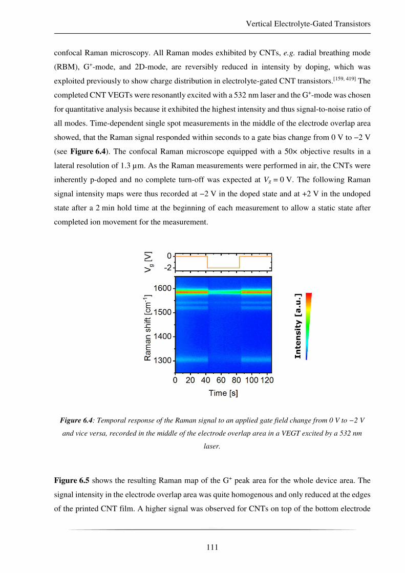
Vertical Electrolyte-Gated Transistors
111
confocal Raman microscopy. All Raman modes exhibited by CNTs, e.g. radial breathing mode
(RBM), G+-mode, and 2D-mode, are reversibly reduced in intensity by doping, which was
exploited previously to show charge distribution in electrolyte-gated CNT transistors.[159, 419] The
completed CNT VEGTs were resonantly excited with a 532 nm laser and the G+-mode was chosen
for quantitative analysis because it exhibited the highest intensity and thus signal-to-noise ratio of
all modes. Time-dependent single spot measurements in the middle of the electrode overlap area
showed, that the Raman signal responded within seconds to a gate bias change from 0 V to −2 V
(see Figure 6.4). The confocal Raman microscope equipped with a 50× objective results in a
lateral resolution of 1.3 µm. As the Raman measurements were performed in air, the CNTs were
inherently p-doped and no complete turn-off was expected at Vg = 0 V. The following Raman
signal intensity maps were thus recorded at −2 V in the doped state and at +2 V in the undoped
state after a 2 min hold time at the beginning of each measurement to allow a static state after
completed ion movement for the measurement.
Figure 6.4: Temporal response of the Raman signal to an applied gate field change from 0 V to −2 V
and vice versa, recorded in the middle of the electrode overlap area in a VEGT excited by a 532 nm
laser.
Figure 6.5 shows the resulting Raman map of the G+ peak area for the whole device area. The
signal intensity in the electrode overlap area was quite homogenous and only reduced at the edges
of the printed CNT film. A higher signal was observed for CNTs on top of the bottom electrode

Vertical Electrolyte-Gated Transistors
112
acting as a mirror while a decreased intensity for areas below the top electrode was found.
However, the very thin top electrode (20 nm gold) that was still semi-transparent was used and
enabled spectral acquisition and peak fitting even in the doped state as shown in the representative
spectra. Peak fitting only became unreliable for very thin nanotube layers at the edges of the film.
The resulting non-reliable intensity ratios were excluded from the final maps.
Figure 6.5: Raman map of G+-band peak area (left top), ratio of the G+-band peak area of doped to
undoped state (left bottom) and representative Raman spectra at different positions of the VEGT
(right).
The ratio of the G+ peak area in the doped vs the undoped state was very uniform at less than 0.15
throughout the whole device area. Although the electrodes were still slightly visible due to less
efficient doping below the top electrode, i.e. an increased signal ratio, even at positions in the
middle of the electrode overlap and thus around 100 µm away from the electrode edges the doping
effect was clearly visible. The same measurements were repeated for a smaller electrode width of

Vertical Electrolyte-Gated Transistors
113
around 100 µm and showed similar results independent from the nanotube film thickness as
depicted in Figure 6.6. The decreased Raman signal below the top electrode was still clearly
visible. For very thick films the mirror effect of the bottom electrode, i.e. the increased signal
observed at low d, was not relevant anymore. The aerosol-jet printed network of CNTs was thus
suitable for electrolyte gating with an ion-gel even for feature sizes of several hundred microns
and a wide range of film thicknesses. It was not necessary to introduce and later remove any filler
as the nanotube network inherently showed a sufficiently high porosity for the electrolyte ions.
The final performance of the produced VEGTs will be discussed in detail in the next section.
Figure 6.6: Raman maps of normalized G+ peak area (top row). The ratio of the G+ peak area of
doped to undoped state is shown in the bottom row for CNT layers with a thickness of 602, 307, 116,
and 65 nm (left to right). The average ratios are given in the images and indicate complete doping of
the whole network areas in all samples.
6.3. Device Characteristics of VEGTs
The main advantage of the presented vertical device architecture is the decoupling of the printing
accuracy from the critical device dimension, i.e. the channel length L. As L depends only on the
thickness of the semiconductor, a geometrical channel length of less than 100 nm is easily
possible. However, the short channels also create a major challenge when using CNTs as

Vertical Electrolyte-Gated Transistors
114
semiconducting material. It is still almost impossible to grow solely semiconducting nanotubes or
even single nanotube species. Polymer-wrapping can separate metallic (m-CNTs) from
semiconducting nanotubes quite efficiently when using the right materials and processing
conditions. The residual concentration of m-CNTs can be below the detection limit of optical
characterization tools such as Raman and absorbance spectroscopy.[52, 91, 110, 146, 420] However, for
very short channel lengths as in the vertical architecture, even a few metallic CNTs can severely
reduce the transistor modulation. It was shown for sub-micron channel length transistors, that
even 1 metallic out of a total of 7 nanotubes almost completely prohibits the ability to modulate
the source–drain current of the device via the gate voltage.[421] Even at a channel length of 4 µm,
a content of 5 % metallic CNTs decreased the on/off-ratio to less than 10.[422] Here, CNT film
thicknesses and thus channel lengths of 50 to 600 nm were studied, i.e. a nanotube with an average
length of 1 µm could bridge the top and bottom electrodes at a tilt angle of 3° (for d = 50 nm) or
37° (for d = 600 nm). Given the demonstrated three-dimensionality of the printed network (see
section 6.2), it was thus very likely for a direct connection between the two electrodes to occur
even at very low concentrations of m-CNTs. While the dispersions seemed to consist of solely
(6,5) nanotubes according to absorbance spectroscopy, subsequent Raman analysis in the RBM
region revealed additional semiconducting and also metallic CNT chiralities as depicted in
Figure 6.7.

Vertical Electrolyte-Gated Transistors
115
Figure 6.7: Absorbance spectrum showing only (6,5) CNTs (left) and Raman spectra of a drop-cast
film from the same CNT dispersion revealing more chiralities (right, solid lines) for excitation at 532
(green) and 633 nm (red). For other samples, Raman spectroscopy also resolved slightly increased m-
CNT content (right, dashed green line, excitation at 532 nm) that were not visible in the absorbance
spectra.
While absorbance and even Raman spectroscopy could not resolve very low m-CNT contents
here, the final transistors sometimes showed a significantly increased off-current. For dispersions
with a slightly increased m-CNT content that was visible in the Raman spectra (see Figure 6.7)
further increased off-currents and thus reduced on/off-ratios of less than 10 were observed. These
devices were not used for any further studies as this was an unmistakable evidence for metallic
paths across the channel. This illustrates that even an m-CNT content below the detection limit of
spectroscopic tools was sufficient to have a severe negative impact on the device performance,
mainly the on/off-ratio. Figure 6.8 shows the transfer characteristics of solely semiconducting
CNT devices as well as of devices with different degrees of m-CNT impurities. The sample with
the highest off-current (red) was exceptionally bad while slightly increased off-currents (yellow)
were observed frequently. Although even the slightly reduced on/off-ratio might prevent possible
applications, it was in general not detrimental for the following studies concerned with the on-
currents of the devices. Only devices with severely increased off-currents were excluded from
further analysis.

Vertical Electrolyte-Gated Transistors
116
Figure 6.8: Transfer characteristics at Vds = −100 mV of VEGTs with a negligible m-CNT content
(green) in contrast to devices with CNT layers containing different degrees of m-CNT impurities from
not measurable by Raman spectroscopy (yellow) to a measurable content (red).
The transistor behavior of the VEGT was initially tested with pure ionic liquid instead of an ion-
gel. This should lead to a faster response to the applied gate field in contrast to ions bound in and
thus slowed down by a polymer matrix. The transfer characteristics (see Figure 6.9) showed a
steep subthreshold swing of less than 150 mV/dec as well as high on-currents at low source–drain
bias resulting in an on/off-ratio of more than 104 and on-current densities exceeding 25 A cm−2.
The off-current was limited by the gate leakage which was in the range of 10−8 to 10−7 A, a typical
value for electrolyte gated transistors.[157, 159] Cyclic switching between the on-state at Vg = −2 V
and Vg = 0 V showed a turn-on of the transistor within seconds while the current decreased only
very slowly, i.e. in the timeframe of half an hour, for Vg = 0 V. As evident from the current–
voltage characteristics, the transfer curve was shifted towards positive voltages, thus a faster turn-
off might be expected if positive voltages were applied. The on-currents did not decrease over
time and were stable even after 12 hours of measurement. Immediately after turning on the device,
the gate current indicated capacitive charging and remained at a higher level than without applied
gate voltage. Although the ion movement is faster in the pure ionic liquid, practical devices require
a solid electrolyte such as an ion-gel, which was used for the following devices.

Vertical Electrolyte-Gated Transistors
117
Figure 6.9: Transfer characteristics (left) and switching behavior over several cycles (middle) of an
ionic liquid gated VEGT for Vds = −10 mV. A zoom-in to an on-switching process shows the current
response within seconds to the applied negative gate voltage (right).
The transistor performance with respect to the on-current density should ideally be independent
from the lateral device dimensions but was expected to depend on the CNT film thickness.
Figure 6.10 depicts the different electrode structures used to investigate the geometry-dependent
device characteristics. The bottom electrodes and the side-gate, both consisting of 2 nm chromium
as adhesion layer and 30 nm of gold, were deposited in an electron-beam evaporator and patterned
by photolithography and lift-off. The top electrode (20 nm gold) was always defined using
stainless steel shadow masks in a thermal evaporator. The top electrode masks consisted of two
long electrode stripes with 200 and 100 µm width for the upper and lower set of 7 transistors,
respectively, and were used for all devices. The actual dimensions resulting from shadow mask
deposition were measured individually with an optical microscope due to possible variations
between sample sets. To investigate the influence of the nanotube film thickness, bottom
electrodes with the same widths were used and structured either photolithographically or via
shadow masks. The influence of the device area was examined by varying the bottom electrode
width from 50 to 500 µm, realized by photolithography. The purple regions in the sample layouts
visualize the areas where CNTs were aerosol-jet printed usually exceeding the expected electrode
overlap area by 100 µm on all sides. The area, where nanotubes were deposited may also influence
the device performance. A large excess area might lead to longer ion diffusion paths and thus it

Vertical Electrolyte-Gated Transistors
118
might be necessary to optimize the alignment of the different layers and reduce CNT deposition
to the actual electrode overlap area.
Figure 6.10: Sample layouts to study their impact on the device characteristics: One complete
substrate with 14 VEGTs (top left) and the standard configuration with 100 x 100 and 200 x 200 µm2
electrode overlap (7 VEGTs each, top right) used for determining reproducibility and CNT film
thickness dependence. The variable electrode overlap areas (bottom left) are shown for Wd = 200 µm
(a corresponding structure was used for Wd = 100 µm). Different CNT printing area sizes at constant
electrode width (bottom right) complete the possible geometric variations. The CNT deposition area is
shaded in purple, bottom electrodes are dark gold and top electrodes light gold.
With an electrode overlap area of 200 x 200 µm2, i.e. 0.04 mm2, several samples with printed
square CNT films of edge lengths from 200, 400, 600, and 800 µm were fabricated to evaluate
the possible influence of the size of the printing area. The resulting films exhibited a thickness of
78–97 nm. The transfer characteristics shown in Figure 6.11 already reveal some device-to-

Vertical Electrolyte-Gated Transistors
119
device variations. For a more detailed evaluation, the on-currents were extracted from these curves
and plotted vs the film thickness and the edge length of the printed CNT film. Overall the on-
currents varied from 0.15 to 0.35 mA while 85 % of the samples were within (0.18 ± 0.03) mA.
Furthermore, there was no systematic trend, neither within the small thickness range, nor within
the large variation of the printing area. As there was no visible influence of the CNT printing area,
the final size was a trade-off between alignment tolerance and material consumption. For easy
alignment with the naked eye, the printing area was chosen so that around the electrode overlap
an additional margin of 100 µm in all directions was covered with CNTs. This alignment tolerance
even exceeds the requirements of other printing methods and enables the fabrication of all-printed
devices later.
Figure 6.11: Transfer characteristics of VEGTs at Vds = −100 mV with different areas of CNT
deposition defined by the edge length of the printed squares W (left) and evaluation of the respective
on-currents with respect to the edge length of the printed film (middle) and the CNT film thickness
(right). The data point labels given in the middle and on the right refer to the thickness in nm and W in
µm, respectively.
Next, devices with different film thicknesses were fabricated with an electrode overlap area of
0.04 mm2 and 0.01 mm2. As the channel length should directly depend on the film thickness d, a
decrease of current was expected with increasing d. Devices with CNT films of less than 50 nm
very often resulted in source–drain shorts, most probably due to penetration of the upper gold
electrode through the thin CNT network. This value was thus determined as the minimum film
thickness and films of up to 600 nm were prepared by consecutive printing of several layers. Two

Vertical Electrolyte-Gated Transistors
120
observations could already be made based on the transfer characteristics depicted in Figure 6.12:
The on-currents decreased with increasing thickness as expected and for layers of more than
300 nm a significant increase in hysteresis was observed. The hysteresis may be attributed to
electron traps created by water molecules that were introduced during the printing process in
ambient conditions.[402] Although the devices were annealed at 300 °C in nitrogen atmosphere
prior to spin-coating of the ion-gel, residual water may still be present especially in thick CNT
films. In contrast to the lateral transistors presented in chapter 5, charge transport takes place
through the whole three-dimensional CNT film as the electric double layer forms around each
nanotube. In the lateral devices, charge transport only occurred at the interface of the CNTs with
the dielectric and thus an increased thickness reduced the influence of water trapped on the
substrate surface. Additionally, the material consumption was directly proportional to d and it was
therefore advisable to reduce the film thickness but keep the film thick enough to prevent source–
drain shorts. Extracting the on-current densities for both electrode overlap areas showed the
expected decrease but also revealed a saturation for films thicker than 200 nm. It was also
observed that the current densities were deviating for the two different electrode widths for thin
films while they were almost the same for thicker ones. This was a first hint that transport might
not only occur completely vertical through the device as will be discussed in section 6.4.
Figure 6.12: Thickness-dependent transfer characteristics for CNT films of 51 to 609 nm thickness
with an electrode overlap of 0.04 mm2 (left) and evaluation of respective on-current densities also for
an electrode overlap of 0.014 mm2 at source drain biases of −0.1 V and −1 V (right).

Vertical Electrolyte-Gated Transistors
121
Varying the electrode overlap area from 47 x 50 µm2 to 140 x 500 µm2 was used to further
investigate the influence of the lateral device dimensions. For a constant top electrode width Wd,
the on-currents increased with increasing bottom electrode width as expected. The on-current
densities however followed the opposite trend and decreased with an increasing bottom electrode
width Ws from more than 70 A cm−2 to less than 20 A cm−2 at a source–drain bias of −1 V (see
Figure 6.13). Moreover, the current density for samples with a wider top electrode (140 µm) was
always smaller when comparing devices with the same bottom electrode width. The CNT
dispersion used for printing these devices contained some metallic CNT species as evident from
the off-current plateau which was above the gate leakage. The off-currents at low source–drain
bias were further increased with increasing electrode width as the probability of percolating
metallic paths or individual tubes bridging the whole channel increased with a larger electrode
overlap area. The large influence of the device dimensions on the on-current densities points
towards the large role of non-vertical charge transport pathways which will be discussed in the
following section.
Figure 6.13: Influence of lateral device geometry tested for different electrode overlap areas:
Transfer characteristics for different bottom electrode widths Ws from 50 to 500 µm and constant top
electrode width Wd of 140 µm (left). Evaluation of on-current densities additionally also for
Wd = 47 µm at different source–drain biases of −0.1 V and −1 V (right).

Vertical Electrolyte-Gated Transistors
122
6.4. Lateral Charge Transport Pathways
The thin semiconductor layer in the VEGTs is supposed to strongly favor charge transport in the
vertical direction from the source to the drain electrode. However, the transport along CNTs is
much faster than inter-nanotube charge transfer. Here, relatively long tubes of about 1 µm were
used. These should also enable charge transport pathways at the edges of the electrodes with only
a small number of nanotube–nanotube junctions involved. Figure 6.14 depicts the possible lateral
pathways for charge carriers that were present in the vertical transistors as a consequence of the
device design. In general, a lateral current Iws that depended on the width of the bottom electrode
Ws could be distinguished from Iwd that was related to the top electrode width Wd.
Figure 6.14: Depiction of possible lateral current pathways in top view (top) and cross-sectional
views for Iws (middle) and Iwd (bottom).
Charge transport occurred at the edge of the top electrode through the CNT film towards the
bottom electrode. The current pathway from the edge of the bottom electrode towards the top
electrode that was directly evaporated on the CNT film was especially short as profilometer data
of the electrodes and the CNT film revealed (see Figure 6.15). At the electrode edge, the CNT

Vertical Electrolyte-Gated Transistors
123
film followed the gold slope within 2 µm lateral distance and directly created a lateral transistor
with a rather short channel length and a width of Wd.
Figure 6.15: Height profiles of gold electrode and CNT film (left) with a zoom in at the edge (right)
showing the short lateral channel (~2 µm) at the edge of the bottom electrode.
Assuming the existence of both lateral current pathways, the total current through the device was
composed of three parts: The area dependent vertical current Iarea as well as the 2 lateral
components:
^_` = ^qs + ^` + ^_
The currents along these 3 channels depended on the device dimensions Wd and Ws where ci are
constants:
^qs = ∙ a_ ∙ a
^_ = _ ∙ a_
^` = ` ∙ a
For a larger dataset, different source–drain bias were taken into account by evaluating the on-
conductance G rather than the on-currents using
t = ^_` ∙ Z_FB

Vertical Electrolyte-Gated Transistors
124
and thus resulting into the following equation for the total current:
t = ∙ a_ ∙ a ∙ Z_FB + _ ∙ a_ ∙ Z_FB + ` ∙ a ∙ Z_FB
When one of the lateral dimensions (Wd or Ws) is constant, the equation for the on-conductivity
becomes linear with respect to Wd (or Ws) with a slope of ms (md) and offset of ts (td):
t = $ ∙ a + _& ∙ Z_FB ∙ a_ + ` ∙ Z_FB ∙ a = ` ∙ a_ + A` for Ws = const.
t = $ ∙ a_ + `& ∙ Z_FB ∙ a + _ ∙ Z_FB ∙ a_ = _ ∙ a + A_ for Wd = const.
Linear extrapolation of this data towards Wd = 0 µm (Ws = 0 µm) resulted in values of the on-
conductance for the respective Ws (Wd) as shown in Figure 6.16.
Figure 6.16: Linear extrapolation of on-conductance towards zero electrode width: Wd-dependent
(left) and Ws-dependent (right)
The y-intercepts were then plotted vs the width of the other electrode, i.e. Ws or Wd (see
Figure 6.17). Here the origin of the plot was fixed to (0|0) for the linear fit, as at zero electrode
width for both, top and bottom electrode, no current should flow. From the slope of the linear fits,
the on-conductance solely depending on Ws (Wd) and thus the lateral conductance per micrometer
electrode width was determined as Gs = 3.8 µS µm−1 and Gd = 36 µS µm−1. The significantly
higher value determined for the Wd–dependent conductance supports the existence of a very short
lateral channel presumed from the profilometer data as explained above. Comparing these to the
overall currents through the VEGTs, the share of lateral currents varied between 10 % for small
electrodes, i.e. 47 x 50 µm2, to up to 49 % for the largest measured electrodes of 142 x 500 µm2.
Despite these possibly large contributions by the lateral currents, they did not adversely influence

Vertical Electrolyte-Gated Transistors
125
the device performance. The lateral currents could even be exploited by minimizing the width of
the bottom electrode while utilizing broad top electrodes and thereby taking advantage of Iwd. As
the circumference of this configuration is larger compared to a square electrode overlap with the
same area, the current density is maximized. Additionally, the off-currents increased with
increasing electrode overlap area due to the increased probability of metallic paths. An increased
on/off-ratio could hence be achieved with smaller active areas as the currents through metallic
CNTs did not significantly contribute to the on-currents. Although a certain degree of three-
dimensionality in the nanotube network was assumed from earlier experiments, the high impact
of lateral currents showed that there still was a high number of CNTs with more or less planar
orientation. Charge transport then favors lateral current pathways with a minimum of necessary
hops to bridge the distance in between source and drain electrode.
Figure 6.17: On-conductances at Wd = 0 µm vs Ws (left) and Ws = 0 µm vs Wd (right) including linear
fits. The error bars were derived from the error of the y-intercept in Figure 6.16.
6.5. Comparison to Lateral Transistors
The vertical electrolyte-gated transistors showed on/off-ratios exceeding 104 and high on-currents.
Additionally, they exhibited a significantly smaller footprint than lateral electrolyte-gated (6,5)
CNT transistors that showed comparable on-currents (compare Figure 6.18). A typical lateral
transistor with interdigitated electrodes, channel lengths of 2 to 5 µm, required an active area of
around 0.9 mm2 to reach an on-conductance in the range of 10 mS. The same values were reached
in the vertical architecture with a much smaller area of 0.16 mm2 already including a 100 µm
alignment margin on all sides of the channel area. The actual active area was only 0.04 mm2. For
Vertical Electrolyte-Gated Transistors
126
printed electrodes, the lateral structure would need even more space, as the channel length and
electrode width would increase due to limited printing resolution (compare chapter 7).
Furthermore, the channel width would need to be increased to compensate the larger channel
length and thus lower on-currents. The vertical structure was estimated to be smaller by at least a
factor of 10 considering these necessary alterations. The consumed material – estimated from the
film volume – was similar for the devices compared here: Using a CNT film thickness of 5 to
10 nm for lateral FETs, the CNT film volume was 4500 to 9000 µm3, compared to around
8000 µm³ for a 51 nm thick nanotube film in the VEGT. The necessary CNT volume for the
VEGTs could be further decreased by reducing the alignment margin.
With respect to device performance, subthreshold swings of less than 200 mV dec−1 and onset-
voltages of less than 1 V were observed for both device structures. One drawback of the vertical
architecture were the increased gate currents that were mostly attributed to ionic conductance
between the source/drain and gate electrodes and capacitive charging. The gate currents could
probably be further reduced by optimizing the exact device geometry especially with respect to
the gate electrode. While the lateral FETs were driven with a 2.4 mm2 large side-gate, the VEGTs
were controlled by a common side-gate pad for all 14 transistors on one substrate that had a total
area of around 19 mm2. Adjustment of the gate size, reduction of the distance between gate and
channel (which was around 1.7 mm) and addressing each transistor with an individual gate are
proposed measures to tackle this effect. Considering the integration density of printed devices, the
vertical architecture is promising even before taking into account the possibility of all-printed
devices that will be discussed in the following section.

Vertical Electrolyte-Gated Transistors
127
Figure 6.18: Comparison of device characteristics (left) and layouts (to scale) of a VEGT and an
interdigitated lateral FET (right).
6.6. All-Printed VEGTs
So far, only the semiconducting layer, i.e. (6,5) CNTs, was deposited by aerosol-jet printing while
the electrodes were evaporated and the ion-gel was spin-coated. While printed ion-gels with
similar ionic liquids were reported before,[255] spin-coating was maintained to avoid the additional
optimization process. Other methods such as blade-coating, dip-coating, or spray-coating are
possible alternative deposition methods for the integration of ion-gels in a roll-to-roll process.
Three different materials were evaluated for printed electrodes: mixed metallic/semiconducting
carbon nanotubes (TUBALL) deposited with an airbrush system through shadow masks, aerosol-
jet printed silver nanoparticles and inkjet printed gold nanoparticles (see optical micrographs in
Figure 6.19). For all architectures, the (6,5) CNTs were AJ printed as described before, while a
film thickness of 150 to 250 nm was used to compensate the potential roughness of the bottom
electrode and avoid shorts with the upper electrode. The electrodes were deposited with the same
parameters before or after deposition of the semiconductor followed by the necessary annealing
steps.
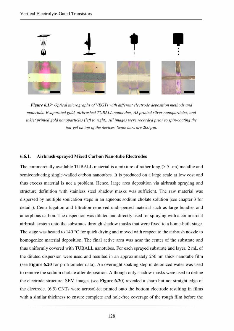
Vertical Electrolyte-Gated Transistors
128
Figure 6.19: Optical micrographs of VEGTs with different electrode deposition methods and
materials: Evaporated gold, airbrushed TUBALL nanotubes, AJ printed silver nanoparticles, and
inkjet printed gold nanoparticles (left to right). All images were recorded prior to spin-coating the
ion-gel on top of the devices. Scale bars are 200 µm.
6.6.1. Airbrush-sprayed Mixed Carbon Nanotube Electrodes
The commercially available TUBALL material is a mixture of rather long (> 5 µm) metallic and
semiconducting single-walled carbon nanotubes. It is produced on a large scale at low cost and
thus excess material is not a problem. Hence, large area deposition via airbrush spraying and
structure definition with stainless steel shadow masks was sufficient. The raw material was
dispersed by multiple sonication steps in an aqueous sodium cholate solution (see chapter 3 for
details). Centrifugation and filtration removed undispersed material such as large bundles and
amorphous carbon. The dispersion was diluted and directly used for spraying with a commercial
airbrush system onto the substrates through shadow masks that were fixed to a home-built stage.
The stage was heated to 140 °C for quick drying and moved with respect to the airbrush nozzle to
homogenize material deposition. The final active area was near the center of the substrate and
thus uniformly covered with TUBALL nanotubes. For each sprayed substrate and layer, 2 mL of
the diluted dispersion were used and resulted in an approximately 250 nm thick nanotube film
(see Figure 6.20 for profilometer data). An overnight soaking step in deionized water was used
to remove the sodium cholate after deposition. Although only shadow masks were used to define
the electrode structure, SEM images (see Figure 6.20) revealed a sharp but not straight edge of
the electrode. (6,5) CNTs were aerosol-jet printed onto the bottom electrode resulting in films
with a similar thickness to ensure complete and hole-free coverage of the rough film before the

Vertical Electrolyte-Gated Transistors
129
top electrode was deposited in similar fashion as the bottom electrode. Shadow masks with
openings of 100 and 200 µm were used and the resulting electrodes were about 10–20 % wider
than that. SEM images of the stack of mixed / (6,5) / mixed nanotubes showed a higher charging
of the semiconducting nanotubes during image acquisition. This enabled the discrimination of the
(6,5) CNTs that appeared brighter in the images than the darker mixed nanotubes that contained
metallic species (see Figure 6.20).
Figure 6.20: Height profiles of the TUBALL electrode (grey) and the (6,5) CNT film (purple)
illustrating a complete coverage (left). SEM images of TUBALL bottom electrode on glass exhibiting a
sharp edge (middle) and TUBALL top electrode on (6,5) CNTs distinguishable by increased charging
of the semiconducting nanotubes (right). Scale bars are 1 µm.
Although the TUBALL nanotubes exhibited sheet resistances of less than 100 Ω −1, voltage
drops along the leads still influenced the device performance, as shown by the much lower drain
currents. Additionally, as shown in Figure 6.21, the conductivity was also modulated by the gate
voltage which was tested by directly spraying the top and bottom electrode on top of each other
without any semiconducting layer between. This was expected due to the relatively large number
of semiconducting nanotubes in the TUBALL electrodes. Although the TUBALL-VEGTs clearly
showed gate modulation of the drain currents, their performance was far from usable and not at
all comparable to those with evaporated gold electrodes.
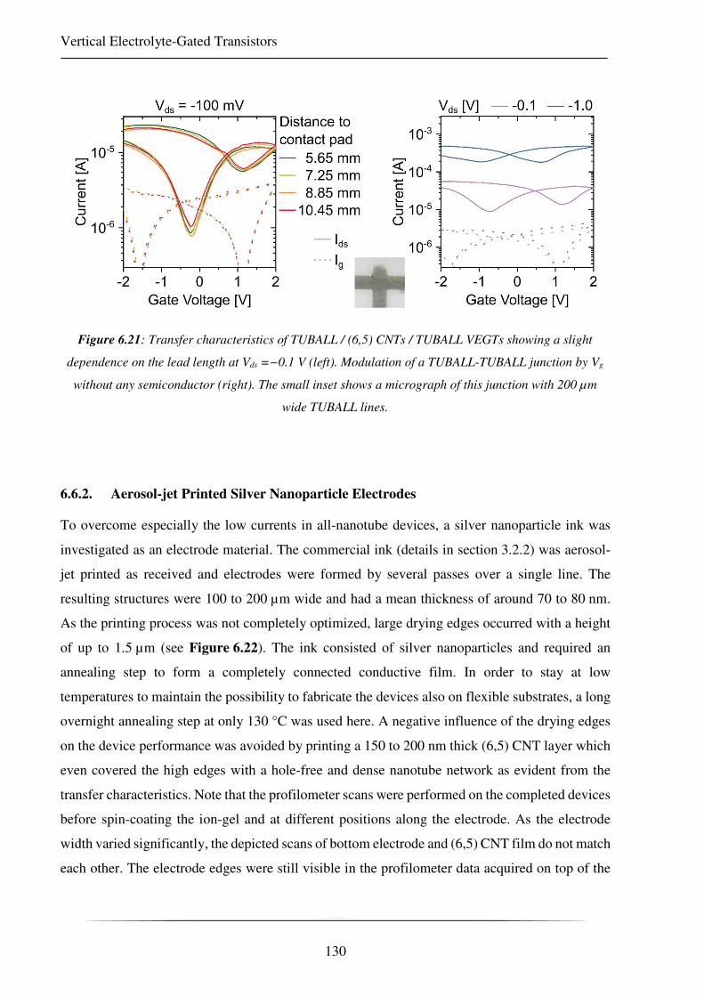
Vertical Electrolyte-Gated Transistors
130
Figure 6.21: Transfer characteristics of TUBALL / (6,5) CNTs / TUBALL VEGTs showing a slight
dependence on the lead length at Vds =−0.1 V (left). Modulation of a TUBALL-TUBALL junction by Vg
without any semiconductor (right). The small inset shows a micrograph of this junction with 200 µm
wide TUBALL lines.
6.6.2. Aerosol-jet Printed Silver Nanoparticle Electrodes
To overcome especially the low currents in all-nanotube devices, a silver nanoparticle ink was
investigated as an electrode material. The commercial ink (details in section 3.2.2) was aerosol-
jet printed as received and electrodes were formed by several passes over a single line. The
resulting structures were 100 to 200 µm wide and had a mean thickness of around 70 to 80 nm.
As the printing process was not completely optimized, large drying edges occurred with a height
of up to 1.5 µm (see Figure 6.22). The ink consisted of silver nanoparticles and required an
annealing step to form a completely connected conductive film. In order to stay at low
temperatures to maintain the possibility to fabricate the devices also on flexible substrates, a long
overnight annealing step at only 130 °C was used here. A negative influence of the drying edges
on the device performance was avoided by printing a 150 to 200 nm thick (6,5) CNT layer which
even covered the high edges with a hole-free and dense nanotube network as evident from the
transfer characteristics. Note that the profilometer scans were performed on the completed devices
before spin-coating the ion-gel and at different positions along the electrode. As the electrode
width varied significantly, the depicted scans of bottom electrode and (6,5) CNT film do not match
each other. The electrode edges were still visible in the profilometer data acquired on top of the

Vertical Electrolyte-Gated Transistors
131
CNT film. Nevertheless, the optical micrographs suggested a complete coverage of the bottom
electrodes.
Figure 6.22: Height profiles showing the large drying edges of the silver ink (grey) that were
nevertheless covered with (6,5) CNTs (purple). Note, that the electrode drying edges varied in width
and height as seen in the optical micrograph with indicated profilometer scan lines (right). The scale
bar in the optical micrograph is 100 µm.
The current–voltage characteristics of these devices again showed an off-current plateau caused
by residual metallic nanotubes even at a very low source–drain bias of −1 mV (see Figure 6.23).
The on/off-ratio was limited by the off-current and values above 103 could only be reached at low
Vds. At increased source–drain bias, the transistor showed on-currents of more than 100 mA, i.e.
on-current densities of up to 570 A cm−2, were realized at Vg = −2 V and Vd = −1 V. The high
currents were attributed to an increased active area due to the drying edges, better wetting behavior
of the aerosol-jet printed ink compared to the thermally evaporated gold, and a thicker electrode
that was less prone to cracks and discontinuities. The turn-on time of the transistors was relatively
short, but complete de-doping – even at slightly positive gate voltages – again required more than
10 minutes. A possible reason for a slow response are the rather small applied electric fields at a
relatively large distance between gate and active area. Additionally, the sponge-like nanotube film
that is only accessible from the sides can hinder fast ion movement.

Vertical Electrolyte-Gated Transistors
132
Figure 6.23: Transfer characteristics of printed Ag / (6,5) CNTs / printed Ag VEGTs for source–drain
biases of −1 mV to −1 V (left). On/off switching cycle of a VEGT at Vds = −10 mV showing the fast
response to Vg = −2 V (on) and slow response over 30 min to Vg = 0.5 V (off).
6.6.3. Inkjet-printed Gold Nanoparticle Electrodes
Besides good wettability for closed CNT films and good contact between semiconductor and
electrode, the contact resistance significantly affects the device performance. The contact
resistance at the metal–nanotube interface was found to be lower for gold than silver.[153] Gold
was thus examined as a third printed electrode material that exhibits a suitable work function. The
number of printable gold nanoparticle inks is limited and not all inks are suitable for all printing
methods. Inkjet printing of a commercial ink was thus chosen as a direct-write approach to define
both, top and bottom, electrodes of the VEGTs. The gold nanoparticle ink was based on a mixture
of water and ethylene glycol and a stage temperature of 60 °C was chosen to dry the ink on the
substrate before the deposition of the subsequent layer. The complete contact structure was inkjet
printed, i.e. the source and drain electrode with a width of around 100 µm, the leads with a width
of 375 µm, the gate electrode, and the contact pads. After printing the bottom electrodes, a
sintering step at 155 °C for several hours was necessary to reduce the overall resistance. The (6,5)
CNT film was printed as described previously before the top electrodes together with the side gate
electrode were printed. The increased width of contact pads and leads as well as the relaxed
resolution needed for these structures enabled a single layer printing process using 5 nozzles in
parallel to deposit a 200–300 nm thick gold film with a low sheet resistance of about 3 Ω −1. For
the electrodes at the active area, i.e. where top and bottom electrode overlapped, a defined width

Vertical Electrolyte-Gated Transistors
133
of around 100–200 µm was required to fabricate VEGTs comparable to the devices presented
before. Thus only a single nozzle was used and 5 parallel lines were printed resulting in an
electrode width of 80–100 µm. Printing of 10 layers reduced the resistance of this fine part of the
electrode but led to a thickness of up to 1.2 µm with a rather rough surface (see profilometer data
in Figure 6.24). The subsequently printed (6,5) nanotube film nevertheless completely covered
the sintered gold and prevented any shorts between top and bottom electrode. Although the surface
of the nanotube film reproduced the roughness of the bottom electrode, the equally thick gold
printed on top formed a conductive electrode as evident from current–voltage characteristics. The
CNT film thickness was estimated from the height differences between a scan on the bottom
electrode next to the active area and a scan over the (6,5) CNT film next to the top electrode. The
resulting data gave a rough estimation of the local thickness but nevertheless depicted the variation
of the film thickness and large roughness of the CNT layer (see Figure 6.24). The average film
thickness calculated from this data was approx. 130 nm and mostly exceeded 100 nm on top of
the bottom electrode.
Figure 6.24: Height profiles of the bottom Au electrode and the (6,5) CNT film on top of it (left) and
the CNT film thickness calculated from the height difference between those two scans (right). Note that
the scans could not be performed at the exact same spot.
The VEGTs completed by ion-gel spin-coating showed no traces of metallic nanotubes as their
off-currents decreased below the gate leakage for source–drain biases of −10 and −100 mV.
Transfer characteristics at higher Vds revealed electron transport resulting in the typical ambipolar
behavior (see Figure 6.25). Although the data shown here were acquired under dry nitrogen
atmosphere, the ambipolar transport persisted upon exposure to air as shown in section 7.2. The

Vertical Electrolyte-Gated Transistors
134
hysteresis of the devices was remarkably low, especially when compared to the other printed
electrode materials shown above. The difference between the turn-on voltage of the forward and
reverse sweep was around 200 mV at Vds = −100 mV for all devices measured with an integration
time of 0.1 s and a gate voltage step size of 50 mV. Repeated switching from the on-state
(Vg = −1.5 V) to the off-state (Vg = +1.5 V) and vice versa illustrated the fast response time within
less than 1 s while maintaining an on/off-ratio of more than 300, mainly limited by the gate-
leakage. The maximum on/off-ratio at Vds = −100 mV even exceeded 104. In contrast to the
previously used structures, the distance to the side-gate was slightly increased while its area was
significantly decreased thus it cannot be the cause of the faster response. One of the most likely
reasons for the slow response observed before was the ion movement within the sponge-like
nanotube film. The thick and thus relatively heavy top gold contact might have compressed the
CNT network and thus limited the length of connected pores into the film. It is however almost
impossible to gain any insight into the actual network without high-resolution three-dimensional
imaging such as electron tomography. Due to the non-transparent gold film on top of the device
it was also not possible to perform the Raman measurements as in chapter 6.2. Although truly
three-dimensional gating and thus charge transport might be limited in these all-printed structures,
the device performance was still remarkable especially with respect to the footprint of the active
area.
Figure 6.25: Transfer characteristics of printed Au / (6,5) CNTs / printed Au VEGTs for source–drain
bias of −10 mV, −100 mV, and −1 V (left). On/off switching cycles of the VEGT at Vds = −100 mV
show the fast response to on- and off-switching at Vg = ±1.5 V.

Vertical Electrolyte-Gated Transistors
135
6.6.4. Comparison of the Different Electrode Materials
A comparison between printed and evaporated gold electrodes illustrates the superior performance
of the inkjet printed gold nanoparticle films. The different fabrication methods resulted in varying
sizes of the geometric electrode overlap, the lead length and the distance between side-gate and
channel area. The measured device characteristics are hence only comparable to a limited extent.
The current density referring to the electrode overlap could at least exclude the influence of the
size of the active area (see Figure 6.26). However, the lateral current pathways and thus the
electrode edges also influenced the total current as discussed in section 6.4. The measured on-
currents nevertheless reflected the same qualitative trends. The on-current densities of printed
gold electrodes exceeded those of evaporated material by about one order of magnitude. The
evaporated electrodes could be limited by the thin (20–30 nm) top contact. Additionally, the
increased roughness of the printed electrodes results in an underestimation of the actual device
area. Using the bulk resistivity of gold (22 nΩ m),[423] the calculated total electrode resistance for
these samples was around 50–100 Ω. The thin gold layer on the rough CNT surface possibly
exhibited discontinuities leading to an actual electrode resistance higher than the calculated
values.
The more than 1 µm thick printed gold film was however unlikely to suffer from discontinuities
and the thereby increased resistance. Conductivity measurements across the whole length of the
inkjet printed gold electrodes revealed a total resistance on the order of 10–100 Ω. In the off-state
of the transistor, this accounted for a comparably low fraction of the overall device resistance.
However, in the on-state, the lead resistance might eventually be limiting the on-currents as the
total resistance of the device in the on-state was around 100 Ω.
Devices fabricated with aerosol-jet printed silver electrodes exhibited the highest current-densities
among the tested materials. While the total electrode length for all gold electrodes was around
15 mm, the printing pattern for aerosol-jet printed silver was optimized to minimize the lead
length to about 1.5 mm in total. Although the resistance could not be measured on those samples,
it was expected to be significantly lower based on reported values of aerosol-jet printed silver
lines exhibiting a resistivity of less than 100 nΩ m.[345, 424] Assuming a cross-section of 50–
100 µm2 based on the profile of the silver electrode the resulting resistance of the silver leads was
in the order of 1–10 Ω and thus about one order of magnitude lower than that of the inkjet printed
gold leads. Here, only the complete devices – including the differences in geometric dimensions
– could be compared. It would be necessary to optimize the printing processes of all electrode

Vertical Electrolyte-Gated Transistors
136
materials to fabricate geometrically identical devices for a comparison of the different CNT–metal
interfaces and their influence on the device performance.
The poorest performance was observed for the nanotube electrodes airbrushed from TUBALL
dispersions. One major drawback of mixed nanotube electrodes might be the limited contact area
between electrode-nanotubes and semiconducting CNTs which was observed before.[425]
Additionally, the sheet resistances were significantly higher than those of the other materials used
here which led to an overall lead resistance of up to several kΩ and a significant voltage drop
across the leads of the device. The resulting current densities were almost two orders of magnitude
lower than for evaporated gold electrodes. The maximum current density achieved in the on-state
was 0.05 A cm−2, compared to 1.7 A cm−2 for evaporated gold, each measured at Vds = −100 mV.
Figure 6.26: Current density (Ids divided by electrode overlap area) at Vds = −100 mV of VEGTs with
different electrode materials: Aerosol-jet printed silver, inkjet printed gold, evaporated gold, and
airbrushed TUBALL nanotubes (highest to lowest on-current density).
As the printed films outperformed the vacuum-deposited gold reaching 15.8 A cm−2 and
55.6 A cm−2 for gold and silver, respectively, they were compared further. The two printed metal
nanoparticle inks showed an almost constant conductivity in the on-state at negative Vg for a
source–drain bias of −10 mV to −1 V. The devices with silver electrodes surpassed the VEGTs
with printed gold by a factor of 4–5 (see Figure 6.27). However, they also exhibited an increased
conductivity in the off-state, especially at Vds = −1 V. The highest on-conductivities were reached
at Vg = −2 V with 6.9 S mm−2 and 1.6 S mm−2 for silver and gold electrodes, respectively. As
discussed before, the conductivity in the on-state was most probably limited by the lead resistance

Vertical Electrolyte-Gated Transistors
137
which was significantly smaller for the silver electrodes due to the device design with very short
contacts. The output characteristics (see Figure 6.27) showed a linear behavior for low source–
drain voltages for both devices. Besides identical lead dimensions, a thorough analysis of contact
resistances would require either different channel lengths with identical three-dimensional
networks, or voltage probes within the channel. As both options are hard to realize with the
vertical device structure, no reliable information about the contact resistance can be given here.
Furthermore, the printed metal films could form a film partly wrapping around nanotubes at the
top electrode. This increased contact area was shown to be beneficial to reduce the contact
resistance.[153] Considering the bottom electrode, the increased roughness – compared to the
evaporated metals – might additionally improve charge injection by electric field enhancement.
While short lead lengths (< 2 mm) were used for printed silver electrodes, applications in all-
printed devices beyond individual transistors require longer interconnects. The printed gold
electrodes however exhibited lead lengths of more than 15 mm. The so far limiting resistances
along the gold leads could be overcome by increasing the lead width or thickness. The inkjet
printed gold electrodes were hence chosen for flexible, all-printed carbon nanotube transistors that
will be investigated in the next chapter.

Vertical Electrolyte-Gated Transistors
138
Figure 6.27: Comparison of printed silver (left) and gold (right) electrodes: Area-normalized
conductivity at different source–drain bias (top) and output characteristics (middle, bottom: zoom-in).
Note the different drain voltage scales for silver and gold electrodes.

139
CHAPTER 7
7.FLEXIBLE TRANSISTORS
In this chapter vertical and lateral all-printed CNT
transistors are fabricated on flexible substrates and their
performance is evaluated with respect to bending.

Flexible Transistors
140
This chapter contains yet unpublished results. The gold nanoparticle electrodes used here were
inkjet printed by M. Held (group of Dr. G. Hernández-Sosa at KIT, Karlsruhe, Germany).
7.1. Introduction
Over the past few years it has been shown that carbon nanotubes can be integrated in flexible and
even stretchable devices while still largely maintaining their good charge transport properties (see
section 2.3.2). CNTs were printed with various methods, e.g. inkjet and gravure printing, and
incorporated into devices. In this work, the reproducibility of aerosol-jet printed CNTs in field-
effect transistors was studied (see chapter 5). The vertical device architecture presented in
chapter 6 utilized electrolyte-gating, a method that was also previously used in various flexible
devices.[148, 149, 151, 152, 233, 234, 239, 255, 277] Furthermore, printed electrodes were introduced with this
structure. It should thus be possible to create all-printed, flexible devices by combining these
methods and transferring the manufacturing processes to a flexible substrate.
Flexible vertical device architectures demonstrated previously relied on advanced manufacturing
techniques and are not compatible with printing processes.[426-429] Additionally, either high
voltages were required or low currents were achieved while no gate leakages were reported. In
this chapter, vertical and lateral electrolyte-gated transistors with inkjet printed gold electrodes,
an aerosol-jet printed CNT semiconductor, and drop-cast ion-gels on flexible plastic substrates
are presented. The two device architectures with identical materials are compared with respect to
their footprint at similar on-conductances, switching behavior in inert and ambient atmosphere as
well as their response to repeated bending.
7.2. Vertical and Lateral CNT Transistors Directly Printed on Plastic Substrates
The all-printed VEGTs presented in section 6.6 were prepared on polyethylene naphthalate (PEN)
foils (thickness 125 µm) cut into 20x25 mm2 pieces, i.e. the same substrate size as the glass used
before. The PEN foil is stable at temperatures below 160 °C and resists at least temporary
exposure to solvents such as isopropanol, toluene, and THF. It is thus compatible with the
temperatures required during printing (up to 100 °C) and annealing (155 °C) and can withstand
the chemicals used for cleaning, printing, and subsequent rinsing. In addition to the vertical
devices, lateral electrolyte-gated transistors (LEGTs) were fabricated and analyzed. The sample

Flexible Transistors
141
layout for both structures is depicted in Figure 7.1. The gold electrodes were inkjet printed with
a subsequent annealing step while the (6,5) nanotubes were aerosol-jet printed followed by careful
rinsing with THF and IPA in each case. 10 layers of CNTs were printed from an initial ink
concentration of 3.0 mg L−1 to reach a thickness of around 150 nm for the VEGTs. The LEGT
electrodes were covered with 2 layers printed from the same CNT dispersion at a concentration
of 1.5 mg L−1. The printing pattern in both cases was a rectangular grid with a line-spacing of
25 µm thus ensuring a dense network over the whole channel area. The channel length of the
lateral devices was around 50 µm as defined by the distance between the gold electrodes. The
relatively large channel length was chosen to prevent source–drain shorts due to ink spills or
uneven edges. For the vertical transistors, the channel length was defined by the CNT film
thickness and thus around 130 nm as discussed in section 6.6. The ion-gel was drop-cast instead
of spin-coated on top of the devices after annealing for at least 1 hour at 150 °C under nitrogen
atmosphere.
Figure 7.1: Sample layout for vertical (left) and lateral (right) electrolyte-gated transistors on flexible
PEN substrates. The printed CNTs are colored purple and the drop-casted ion-gel is grey.
For the electrical characterization of the initial transistor properties, the devices were kept within
nitrogen atmosphere, but had to be exposed to air for bending experiments later (see section 7.3).
Both device architectures showed comparable device performances as evident from the transfer
characteristics (see Figure 7.2). The on-currents for holes were within the same order of
magnitude, i.e. (9.6 ± 0.3) mA and (6.2 ± 0.4) mA were obtained at Vds = −1 V for VEGTs and
LEGTs, respectively. The off-currents were on average around 100 nA for VEGTs and twice as
high for the lateral architecture which might be explained by the larger ion-gel and electrode areas
leading to increased ionic and capacitive currents in the device. Although the LEGTs showed a

Flexible Transistors
142
lower turn-on voltage (50 to 450 mV) for the sweep from the off- towards the on-state, the
variations between individual transistors and the hysteresis were larger. The VEGTs showed
almost identical transfer characteristics with a turn-on voltage of 550 mV measured at
Vds = −100 mV. It should be noted that the hysteresis decreased after repeated measurement of the
transfer characteristics in inert atmosphere for all devices. Figure 7.2 illustrates this for
representative transistors with the 1st set of measurements shown together with the 5th or 3rd set of
measurements for the same VEGT or LEGT, respectively. The depicted transfer characteristics
were measured with the same settings, i.e. an integration time of 0.1 s and gate voltage steps of
0.05 V, while different gate voltage steps and integration times were used between these
measurements. The hysteresis was further decreased during subsequent measurements that were
performed in air after storing the devices under nitrogen atmosphere overnight (compare
Figure 7.4).
Figure 7.2: Representative transfer characteristics of a VEGT (left) and an LEGT (right) at a source–
drain bias of −100 mV and −1000 mV. For both devices, the 1st measurement is shown (red and light
green) together with the 5th (VEGT) or 3rd (LEGT) measurement of a transfer characteristics (yellow
and dark green) performed with the same settings, illustrating the decrease of hysteresis after
repeated measurements.
The response of the device to the applied gate voltage in electrolyte-gated devices generally
depends on the sweep rate as the velocity of the ion drift within the ion-gel is limited. The
transistors closest to the gate pad were measured at Vds = −100 mV with different gate voltage

Flexible Transistors
143
steps ∆Vg of 0.01 V to 0.1 V to evaluate the influence of the sweep rate (see Figure 7.3). Both
devices exhibited basically unchanged turn-on voltages for all sweep rates. With larger gate
voltage steps the turn-off of the transistor shifted towards more positive gate voltages and the
hysteresis increased significantly. Remarkably, the hysteresis was generally lower for the vertical
architecture. Even a measurement with a gate voltage step of 0.5 V resulted in clearly visible
switching of the device, although with further increased hysteresis. The on-currents were
reproducible for all gate voltage step widths while the off-currents increased slightly due to higher
gate leakages caused by capacitive charging. Although the smallest used ∆Vg resulted in the least
hysteresis, the duration of a single measurement was around 10 min for these settings. For further
experiments a step size of 0.05 V was chosen as compromise between hysteresis and duration of
the measurement.
Figure 7.3: Transfer characteristics depending on the gate voltage step width (0.01 V to 0.5 V, green
to red) acquired for the VEGT (left) and LEGT (right) closest to the gate pad at Vds = −100 mV.
Both types of electrolyte-gated transistors were able to reach on-currents of several mA while
maintaining an off-current level in the µA regime. It should thus be possible to drive light-emitting
diodes (LEDs) with these transistors, as the required currents are in the same range even for large
area display backplanes.[430] For visualization of the switching process the source and drain
contacts were connected in series with a red LED. Due to the voltage drop across the diode, a total
external potential of −2.5 V was applied. Figure 7.4 shows the resulting transfer characteristics
with on-currents around 5 mA. During a gate voltage sweep, the intensity of the LED could be
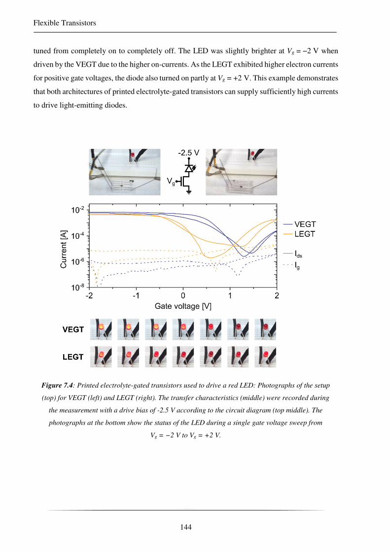
Flexible Transistors
144
tuned from completely on to completely off. The LED was slightly brighter at Vg = −2 V when
driven by the VEGT due to the higher on-currents. As the LEGT exhibited higher electron currents
for positive gate voltages, the diode also turned on partly at Vg = +2 V. This example demonstrates
that both architectures of printed electrolyte-gated transistors can supply sufficiently high currents
to drive light-emitting diodes.
Figure 7.4: Printed electrolyte-gated transistors used to drive a red LED: Photographs of the setup
(top) for VEGT (left) and LEGT (right). The transfer characteristics (middle) were recorded during
the measurement with a drive bias of -2.5 V according to the circuit diagram (top middle). The
photographs at the bottom show the status of the LED during a single gate voltage sweep from
Vg = −2 V to Vg = +2 V.
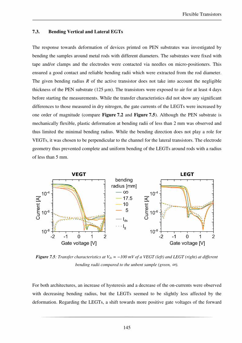
Flexible Transistors
145
7.3. Bending Vertical and Lateral EGTs
The response towards deformation of devices printed on PEN substrates was investigated by
bending the samples around metal rods with different diameters. The substrates were fixed with
tape and/or clamps and the electrodes were contacted via needles on micro-positioners. This
ensured a good contact and reliable bending radii which were extracted from the rod diameter.
The given bending radius R of the active transistor does not take into account the negligible
thickness of the PEN substrate (125 µm). The transistors were exposed to air for at least 4 days
before starting the measurements. While the transfer characteristics did not show any significant
differences to those measured in dry nitrogen, the gate currents of the LEGTs were increased by
one order of magnitude (compare Figure 7.2 and Figure 7.5). Although the PEN substrate is
mechanically flexible, plastic deformation at bending radii of less than 2 mm was observed and
thus limited the minimal bending radius. While the bending direction does not play a role for
VEGTs, it was chosen to be perpendicular to the channel for the lateral transistors. The electrode
geometry thus prevented complete and uniform bending of the LEGTs around rods with a radius
of less than 5 mm.
Figure 7.5: Transfer characteristics at Vds = −100 mV of a VEGT (left) and LEGT (right) at different
bending radii compared to the unbent sample (green, ∞).
For both architectures, an increase of hysteresis and a decrease of the on-currents were observed
with decreasing bending radius, but the LEGTs seemed to be slightly less affected by the
deformation. Regarding the LEGTs, a shift towards more positive gate voltages of the forward

Flexible Transistors
146
sweep (−2 V → +2 V) during bending at R = 17.5 mm occurred and remained thereafter. In
contrast to that, the reverse sweep (+2 V → −2 V) shifted continuously with decreasing R towards
more negative Vg and thereby increased the hysteresis in VEGTs. However, the on-currents also
decreased (compared to the measurement performed at R = 5 mm) with a subsequent
measurement in the unbent position while the hysteresis remained unchanged (see Figure 7.6). It
should be noted that the sequence of measurements was from the unbent status towards smaller
bending radii. The measurement of 10 consecutive transfer characteristics at R = ∞ also resulted
in continuously decreasing on-currents yet constant hysteresis. Hence, the previously observed
changes in on-currents cannot be reliably attributed to the bending of the devices but might also
be a degradation effect of the devices during repeated measurements in air.
Figure 7.6: The influence of repeated measurements of transfer characteristics at Vds = −100 mV for
a VEGT (left) and an LEGT (right) can be seen when returning to a flat substrate after bending (top)
as well as in consecutive measurements of the same device without bending (bottom).
Flexible Transistors
147
In addition to stable device performance at different bending radii, it is also important that the
devices can withstand repeated bending. The VEGTs were thus bent automatically from R = ∞ to
R ≈ 5 mm and measured in the flat position at the beginning and after 100 and 1000 cycles. The
same experiment was repeated for the LEGTs with measurements after 100 and 680 cycles. The
lower cycle number here originates from a detachment of the sample from the machine used for
bending during the experiment. The transfer characteristics exhibited a constant hysteresis for all
devices (see Figure 7.7) and successively decreasing on-currents for the LEGTs. Measurements
at Vds = −1 V overall showed a current decrease by a factor of 2 for hole as well as electron
transport. The VEGTs however exhibited increasing on-currents and a slight shift of the entire
transfer curve towards more positive gate voltages. Measurements at higher source-drain bias
reproduced the same trend with additionally increasing electron current at positive gate voltages.
The overall increased currents might originate from a deformation of the CNT film, e.g. decreased
thickness, thus shortening of the effective length of charge-transport paths through the vertical
channel. Additionally, doping by oxygen and water from ambient air might increase during
bending and thus cause these effects.[431, 432] Overall, the observed changes were relatively small
with an average increase of the on-currents by a factor of 1.3 and a shift of the turn-on voltages
of 150 mV. Especially the vertical architecture seems to be almost unaffected by repeated
bending, however, the issue of decreasing currents with repeated measurements remains to be
solved. As this phenomenon only occurred during measurements in air, encapsulation of the
device might already be sufficient.

Flexible Transistors
148
Figure 7.7: Change of transfer characteristics at Vds = −100 mV for repeated bending to a radius of
5 mm for a VEGT (left) and an LEGT (right). The measurements were performed in the unbent
position before (green) and after 100 (yellow) and 1000 (VEGT, red) or 680 (LEGT, red) bending
cycles.
Both device architectures exhibited similar properties with respect to the achievable on-currents,
operation voltages, and persistence to deformation as shown in this chapter. Depending on the
individual measurement, the performance of the lateral or the vertical transistors seemed to be
superior with slight advantages for the VEGTs. For fabrication on the flexible PEN substrates, the
same materials were used, i.e. inkjet printed gold electrodes, aerosol-jet printed (6,5) CNTs, and
the drop-cast ion-gel containing [EMIM][FAP] and P(VDF-HFP). While the channel length of
the lateral transistors was limited by the inkjet printing process, the relatively thin CNT film
enabled high on-currents and a small footprint for the vertical structure. The active area necessary
for comparable on-currents in the lateral transistors was around 0.5 mm2, in contrast to less than
0.01 mm² for the VEGTs. Including the area of electrodes and – in the case of the vertical
architecture – the increased area of CNTs to ensure a sufficient alignment margin, the total
footprint of the devices was around 0.1 mm2 and 3.4 mm2 for VEGTs and LEGTs, respectively.
This difference in footprint demonstrates again the potential of the vertical architecture with
semiconducting CNTs for all-printed transistors in applications where electrolyte-gating is
feasible.
The combination of flexibility, printability, and high on-currents for a small device footprint
highlights the advantages of VEGTs compared to earlier reports. Previous lateral transistors with

Flexible Transistors
149
similar on-conductances as the vertical transistors either required photolithographic
structuring,[284, 433] or additional processing steps such as CNT transfer and subsequent etching,[220,
433] each in combination with higher operation voltages of 5 to 100 V. Another report on a lateral
architecture with a footprint comparable to the printed LEGT relied on transfer of the evaporated
gold electrodes from a PDMS stamp onto the flexible substrate to form the short channel lengths
of 5 µm necessary to reach the corresponding on-conductances.[434] All-printed devices used either
a composite of barium titanate and PMMA or ion-gels to ensure the printability and flexibility of
the dielectric layer.[147, 152, 221, 267] While the devices with composite dielectrics showed stable
device performances over extended storing periods and up to 1000 measurement cycles, the area-
normalized on-conductances were several orders of magnitude lower.[147, 221] Moreover, although
the devices were fabricated on flexible substrates, there was either no information about bending
experiments at all,[221] or data concerning the device performance with respect to repeated bending
was missing.[147] Electrolyte-gated devices were suffering from extremely low on/off-ratios of
only 138, [267] or additional nanoimprinting was required to define the electrode printing area more
exactly,[152] yet only low on-conductances could be reached. Unfortunately, many reports do not
provide information about the change of device performance with respect to bending, especially
with respect to repeated bending. However, using photolithographically structured electrodes,
inverters that showed an extremely good stability even after bending more than 1000 times to a
bending radius as low as 1.27 mm, were demonstrated.[284] Concerning all-printed devices,
bending to radii as small as 1 mm was presented without significant change of the transistor
characteristics.[147] In conclusion, the here fabricated all-printed VEGTs with gold nanoparticle
electrodes, but also the LEGTs, performed extremely well with high on-conductances while being
resistant to bending.

150

151
CHAPTER 8
8.CONCLUSIONS AND OUTLOOK
In this chapter the insights gained in this thesis are
summarized and an outlook for further experiments and
applications based on aerosol-jet printed transistors with
CNTs is given.

Conclusions and Outlook
152
The goal of this thesis was to establish printed CNT networks as semiconductors in fully printed
and flexible transistors. To achieve this goal, aerosol-jet printing was demonstrated to be a
versatile tool to create directly patterned films of semiconducting (6,5) carbon nanotubes with
variable thickness. These films were successfully incorporated in different field-effect and
electrolyte-gated transistors with lateral or vertical charge transport through the semiconductor.
Eventually, all-printed transistors were fabricated on plastic substrates and stable performance
even after bending stress was observed.
As a first step, the composition of the ink based on polymer-wrapped carbon nanotubes in toluene
for aerosol-jet printing was investigated. The addition of terpineol resulted in good printability.
However, the influence of varying CNT concentration – and hence slightly altered viscosity – on
the aerosolization and deposition process requires further studies. An examination of the stability
of the nanotubes during the printing process over time showed that the sonication strength of the
ultrasonic atomizer was low enough to avoid damage to the dispersed (6,5) CNTs, but still
powerful enough to create a dense aerosol. The observed long-time stability corroborated the
suitability of aerosol-jet printing for large-area and reproducible deposition of CNT for electronic
devices. The ultrasonic atomizer requires relatively small ink volumes and offers the possibility
to test materials that are only available in small quantities and for small sample numbers, it is thus
well-suited for lab-scale experiments. The alternative pneumatic atomizer is even gentler and can
process larger ink volumes, hence aerosol-jet printing of CNTs is also promising with respect to
future upscaling and large area printing.
The aerosol-jet printed films of (6,5) carbon nanotubes were used in an established top-gate field-
effect transistor geometry. The achieved reproducibility of dense but thin networks was
comparable to previously published results for CNT films prepared from dispersion, i.e. by spin-
coating, dip-coating, or immersion. An increased thickness of the CNT films resulted in a
significantly decreased hysteresis as well as increased mobilities and on-conductance while
maintaining low off-currents. Thickness control was achieved by altering the printing pattern and
number of layers without changing the ink composition, hence the improved device performance
was achieved at the expense of increased processing times and material consumption.
Nevertheless, the established printing parameters could be kept basically constant. For sparse
CNT networks, aerosol-jet printing resulted in a large variation in local density. With the process
developed in this work, a precise control of low CNT coverage was not possible. However, dense
films could be produced with variable thickness and also for different carbon nanotube types

Conclusions and Outlook
153
dispersed in toluene with respective wrapping polymers. Such printed films have already been
used in various studies, e.g. for electrochromic devices, and are interesting for further applications
in printed circuitry and sensing.
For all-printed transistors the resolution and alignment accuracy was considered as the limiting
factor. In lateral architectures, i.e. with current flow across the channel parallel to the substrate,
the achievable conductances are limited by the channel dimensions. While a large channel width
increases the total current along with device footprint, short channel lengths are restricted by the
printing processes. Based on a recently reported vertical architecture, thick CNT films were
printed between a bottom source and an overlapping top drain electrode, resulting in current flow
perpendicular to the substrate using electrolyte-gating. The CNT network exhibited a sufficient
porosity to enable electrolyte-gating even for overlapping electrode areas with edge lengths of
several hundred micrometers. The sponge-like nanotube film and low electric fields resulted in a
response time of the transistors in the range of seconds to minutes. Three-dimensional charge
transport could be assumed for CNT films with a thickness of up to several hundred nanometers.
Aerosol-jet printed (6,5) CNT films with a thickness of 100–200 nm were free of source–drain
shorts even for printed electrodes with a large roughness. Although most of the current was
transported vertically between source and drain electrode, the electrode edges played an important
role as well. Depending on the electrode dimensions, up to almost 50 % of current were conducted
across quasi-lateral channels at the electrode edges. However, this observation does not invalidate
the usability of the vertical device architecture as the decoupling of critical device dimensions
from the printing accuracy was still achieved. Moreover, the vertical transistors outperformed
comparable electrolyte-gated lateral short-channel transistors with photographically structured
electrodes and printed nanotubes while exhibiting a more than 10-fold smaller footprint.
While the transport within the printed semiconducting layer was fairly reproducible, the measured
on-conductance depended strongly on the electrode material (evaporated or printed, metal or
mixed CNTs). In addition to the lead resistance and contact at the semiconductor–conductor
interface, the actual geometric device dimensions probably had an impact on the overall
performance. Especially variations of the dimensions of the channel area, electrode cross-section,
and lead length caused by different deposition methods made a one-to-one comparison of the
devices difficult or impossible. Moreover, the printing parameters were not entirely optimized for
the electrode materials (mixed CNTs or colloidal silver nanoparticles) and drying edges as well
as ohmic losses due to the total resistance of the conductors occurred. Nevertheless, aerosol-jet

Conclusions and Outlook
154
printing of a porous CNT film for vertical electrolyte-gated transistors was found to be compatible
with different printed electrode materials. With adapted electrode geometries and printing
parameters, fully printed devices should become reproducible and competitive. Optimizing the
device design especially with respect to the side-gate dimensions and individual addressing of
each transistor will further improve transistor performance. The use of printed electrodes here
simplifies the refinement process as pattern changes can be easily implemented and tested.
All-printed vertical and lateral transistors were also manufactured on flexible PEN substrates with
inkjet printed gold electrodes. While both device types showed good transfer characteristics, the
lateral transistors required a 30 times larger footprint to achieve on-currents comparable to those
of vertical transistors. Both architectures were largely resistant to repeated outward bending
(tensile strain) but unfortunately showed degradation during measurement in air. The total on-
currents were sufficiently high to drive a red LED and outperformed previously reported values
for transistors with printed CNTs. However, the devices presented here only showed the proof-
of-concept and further experiments are necessary to reveal their full potential. Future work on
flexible aerosol-jet printed nanotube transistors should also include inward and outward bending.
Furthermore, the device performance should be evaluated after bending along different directions.
While it is expected that a potential performance change does not depend on the bending direction
for the vertical devices, the lateral transistors might show differences upon bending parallel or
perpendicular to the channel. Encapsulation might be helpful to avoid degradation in air and
additionally prevent possible detachment of structures from the substrate. The minimum bending
radius could be further improved with alternative substrate materials such as silicone elastomers
that enable three-dimensional deformation with sub-millimeter bending radii and possibly
stretchability.[282] With these substrates, the true limitations especially of VEGTs could also be
evaluated. So far, it remains unclear, how tolerant the transistors are to wrinkling, folding, and
stretching. The limiting factor for these investigations was the necessity of mechanically stable
and conductive electrodes on ultra-flexible and stretchable substrates while nanotube networks
are expected to be ideal for all kinds of deformations. Although stretchable conductors have been
presented before, the adoption of the respective processes was beyond the scope of this thesis.
Preliminary experiments on aerosol-jet printing of CNTs on stretchable substrates already resulted
in closed and stable films that were visible to the naked eye. With suitable electrodes, stretchable
devices based on aerosol-jet printed nanotubes should thus be feasible.

Conclusions and Outlook
155
Within this thesis, the suitability of carbon nanotubes for vertical electrolyte-gated transistors was
demonstrated. The response time of the electrolyte-gated, three-dimensional CNT networks
presented in this work was too long for high-frequency applications. Optimization of the entire
device geometry could however further improve the device performance and enable integrated
circuits. Additionally, the compatibility of this architecture to printing processes in combination
with electrolyte-gating offers the opportunity for high throughput – and thus low-cost – fabrication
of single-use sensors. The high drain-currents that were achieved would simplify the readout.
CNTs have already been successfully used for electrostatic biosensing,[158] and similar
functionality should be possible for the vertical transistors. Especially for sensing applications,
the reproducibility of devices is not as critical as calibration experiments are usually performed
prior to the actual measurement.
The already good reproducibility of the performance of aerosol-jet printed CNT transistors could
be further improved by ensuring an optimized and steady ink composition. To achieve that, the
influence of different ink parameters, e.g. material loading, filling level, and viscosity, on the
aerosol formation and composition should be further investigated. Continuous monitoring of the
ink composition may enable tailored addition of nanotube dispersion or solvents to obtain a
constant filling level and ink formulation over extended printing times.
In this work, aerosol-jet printing of semiconducting CNTs for different transistor architectures
was demonstrated with promising results even on flexible substrates. Optimized processing and
device geometries could further improve the transistor performance. In conclusion, this work
represents another step towards the successful utilization of fully printed transistors based on
carbon nanotubes for a variety of applications.

156

157
BIBLIOGRAPHY
[1] J. Zaumseil, "Single-walled carbon nanotube networks for flexible and printed
electronics". Semicond. Sci. Technol., 2015, 30, 074001. https://doi.org/10.1088/0268-
1242/30/7/074001
[2] Q. Cao, S.-J. Han, G. S. Tulevski, A. D. Franklin, W. Haensch, "Evaluation of Field-
Effect Mobility and Contact Resistance of Transistors That Use Solution-Processed
Single-Walled Carbon Nanotubes". ACS Nano, 2012, 6, 6471.
https://doi.org/10.1021/nn302185d
[3] M. Held, P. Laiho, A. Kaskela, F. Gannott, M. Rother, E. Kauppinen, J. Zaumseil,
"Dense Carbon Nanotube Films as Transparent Electrodes in Low‐Voltage Polymer and
All‐Carbon Transistors". Adv. Electron. Mater., 2017, 1700331.
https://doi.org/10.1002/aelm.201700331
[4] A. G. Nasibulin, A. Kaskela, K. Mustonen, A. S. Anisimov, V. Ruiz, S. Kivistö, ..., E. I.
Kauppinen, "Multifunctional Free-Standing Single-Walled Carbon Nanotube Films".
ACS Nano, 2011, 5, 3214. https://doi.org/10.1021/nn200338r
[5] B. King, M. Renn, "Aerosol Jet® Direct Write Printing for Mil-Aero Electronic
Applications", presented at Palo Alto Colloquia, Lockheed Martin, 2009.
[6] A. Hirsch, "The era of carbon allotropes". Nat. Mater., 2010, 9, 868.
https://doi.org/10.1038/nmat2885
[7] H. W. Kroto, J. R. Heath, S. C. O'Brien, R. F. Curl, R. E. Smalley, "C60:
Buckminsterfullerene". Nature, 1985, 318, 162. https://doi.org/10.1038/318162a0
[8] S. Iijima, "Helical microtubules of graphitic carbon". Nature, 1991, 354, 56.
https://doi.org/10.1038/354056a0

Bibliography
158
[9] K. S. Novoselov, A. K. Geim, S. V. Morozov, D. Jiang, Y. Zhang, S. V. Dubonos, ..., A.
A. Firsov, "Electric Field Effect in Atomically Thin Carbon Films". Science, 2004, 306,
666. https://doi.org/10.1126/science.1102896
[10] M. Ezawa, "Peculiar width dependence of the electronic properties of carbon
nanoribbons". Phys. Rev. B, 2006, 73, 045432.
https://doi.org/10.1103/PhysRevB.73.045432
[11] K. Tanaka, K. Ohzeki, S. Nankai, T. Yamabe, H. Shirakawa, "The electronic structures
of polyacene and polyphenanthrene". J. Phys. Chem. Solids, 1983, 44, 1069.
https://doi.org/10.1016/0022-3697(83)90089-6
[12] E. D. Obraztsova, M. Fujii, S. Hayashi, V. L. Kuznetsov, Y. V. Butenko, A. L. Chuvilin,
"Raman identification of onion-like carbon". Carbon, 1998, 36, 821.
https://doi.org/10.1016/S0008-6223(98)00014-1
[13] D. Ugarte, "Curling and closure of graphitic networks under electron-beam irradiation".
Nature, 1992, 359, 707. https://doi.org/10.1038/359707a0
[14] S. Iijima, M. Yudasaka, R. Yamada, S. Bandow, K. Suenaga, F. Kokai, K. Takahashi,
"Nano-aggregates of single-walled graphitic carbon nano-horns". Chem. Phys. Lett.,
1999, 309, 165. https://doi.org/10.1016/S0009-2614(99)00642-9
[15] X. Peng, N. Komatsu, S. Bhattacharya, T. Shimawaki, S. Aonuma, T. Kimura, A. Osuka,
"Optically active single-walled carbon nanotubes". Nat. Nanotechnol., 2007, 2, 361.
https://doi.org/10.1038/nnano.2007.142
[16] A. A. Green, M. C. Duch, M. C. Hersam, "Isolation of single-walled carbon nanotube
enantiomers by density differentiation". Nano Res., 2009, 2, 69.
https://doi.org/10.1007/s12274-009-9006-y
[17] G. Ao, J. K. Streit, J. A. Fagan, M. Zheng, "Differentiating Left- and Right-Handed
Carbon Nanotubes by DNA". J. Am. Chem. Soc., 2016, 138, 16677.
https://doi.org/10.1021/jacs.6b09135
[18] S. Reich, J. Maultzsch, C. Thomsen, P. Ordejón, "Tight-binding description of
graphene". Phys. Rev. B, 2002, 66, 035412. https://doi.org/10.1103/PhysRevB.66.035412
[19] R. Saito, G. Dresselhaus, M. S. Dresselhaus, Physical properties of carbon nanotubes,
Imperial College Press, London 1998.
[20] S. Reich, C. Thomsen, J. Maultzsch, Carbon nanotubes: basic concepts and physical
properties, John Wiley & Sons, Weinheim 2008.

Bibliography
159
[21] S. Ilani, P. L. McEuen, "Electron Transport in Carbon Nanotubes". Annu. Rev. Condens.
Matter Phys., 2010, 1, 1. https://doi.org/10.1146/annurev-conmatphys-070909-103928
[22] M. Huang, Y. Wu, B. Chandra, H. Yan, Y. Shan, T. F. Heinz, J. Hone, "Direct
Measurement of Strain-Induced Changes in the Band Structure of Carbon Nanotubes".
Phys. Rev. Lett., 2008, 100, 136803. https://doi.org/10.1103/PhysRevLett.100.136803
[23] E. D. Minot, Y. Yaish, V. Sazonova, J.-Y. Park, M. Brink, P. L. McEuen, "Tuning
Carbon Nanotube Band Gaps with Strain". Phys. Rev. Lett., 2003, 90, 156401.
https://doi.org/10.1103/PhysRevLett.90.156401
[24] G. G. Samsonidze, A. R. Saito, D. A. Jorio, E. Pimenta, F. Souza, F. A. Grüneis, ..., M.
Dresselhaus, "The concept of cutting lines in carbon nanotube science". Journal of
Nanoscience and Nanotechnology, 2003, 3, 431. https://doi.org/10.1166/jnn.2003.231
[25] J.-C. Charlier, X. Blase, S. Roche, "Electronic and transport properties of nanotubes".
Rev. Mod. Phys., 2007, 79, 677. https://doi.org/10.1103/RevModPhys.79.677
[26] R. Saito, G. Dresselhaus, M. S. Dresselhaus, "Trigonal warping effect of carbon
nanotubes". Phys. Rev. B, 2000, 61, 2981. https://doi.org/10.1103/PhysRevB.61.2981
[27] S. Maruyama, 2018, accessed: 11/10/2018, http://www.photon.t.u-
tokyo.ac.jp/~maruyama/kataura/1D_DOS.html
[28] H. Kataura, Y. Kumazawa, Y. Maniwa, I. Umezu, S. Suzuki, Y. Ohtsuka, Y. Achiba,
"Optical properties of single-wall carbon nanotubes". Synth. Met., 1999, 103, 2555.
https://doi.org/10.1016/S0379-6779(98)00278-1
[29] S. M. Bachilo, M. S. Strano, C. Kittrell, R. H. Hauge, R. E. Smalley, R. B. Weisman,
"Structure-Assigned Optical Spectra of Single-Walled Carbon Nanotubes". Science,
2002, 298, 2361. https://doi.org/10.1126/science.1078727
[30] S. Lebedkin, F. Hennrich, T. Skipa, M. M. Kappes, "Near-Infrared Photoluminescence
of Single-Walled Carbon Nanotubes Prepared by the Laser Vaporization Method". J.
Phys. Chem. B, 2003, 107, 1949. https://doi.org/10.1021/jp027096z
[31] R. B. Weisman, S. M. Bachilo, "Dependence of Optical Transition Energies on Structure
for Single-Walled Carbon Nanotubes in Aqueous Suspension: An Empirical Kataura
Plot". Nano Lett., 2003, 3, 1235. https://doi.org/10.1021/nl034428i
[32] S. Maruyama, 2018, accessed: 11/10/2018, http://www.photon.t.u-
tokyo.ac.jp/~maruyama/kataura/kataura.html

Bibliography
160
[33] M. Rother, S. P. Schießl, Y. Zakharko, F. Gannott, J. Zaumseil, "Understanding Charge
Transport in Mixed Networks of Semiconducting Carbon Nanotubes". ACS Appl. Mater.
Interfaces, 2016, 8, 5571. https://doi.org/10.1021/acsami.6b00074
[34] J. Maultzsch, H. Telg, S. Reich, C. Thomsen, "Radial breathing mode of single-walled
carbon nanotubes: Optical transition energies and chiral-index assignment". Phys. Rev.
B, 2005, 72, 205438. https://doi.org/10.1103/PhysRevB.72.205438
[35] A. Jorio, R. Saito, J. H. Hafner, C. M. Lieber, M. Hunter, T. McClure, ..., M. S.
Dresselhaus, "Structural (n,m) Determination of Isolated Single-Wall Carbon Nanotubes
by Resonant Raman Scattering". Phys. Rev. Lett., 2001, 86, 1118.
https://doi.org/10.1103/PhysRevLett.86.1118
[36] P. C. Eklund, J. M. Holden, R. A. Jishi, "Vibrational modes of carbon nanotubes;
Spectroscopy and theory". Carbon, 1995, 33, 959. https://doi.org/10.1016/0008-
6223(95)00035-C
[37] F. Dragin, A. Pénicaud, M. Iurlo, M. Marcaccio, F. Paolucci, E. Anglaret, R. Martel,
"Raman Doping Profiles of Polyelectrolyte SWNTs in Solution". ACS Nano, 2011, 5,
9892. https://doi.org/10.1021/nn203591j
[38] L. Kavan, L. Dunsch, "Spectroelectrochemistry of Carbon Nanotubes". ChemPhysChem,
2011, 12, 47. https://doi.org/10.1002/cphc.201000882
[39] C. Fantini, A. Jorio, M. Souza, M. S. Strano, M. S. Dresselhaus, M. A. Pimenta, "Optical
Transition Energies for Carbon Nanotubes from Resonant Raman Spectroscopy:
Environment and Temperature Effects". Phys. Rev. Lett., 2004, 93, 147406.
https://doi.org/10.1103/PhysRevLett.93.147406
[40] C. A. Cooper, R. J. Young, M. Halsall, "Investigation into the deformation of carbon
nanotubes and their composites through the use of Raman spectroscopy". Composites
Part A: Applied Science and Manufacturing, 2001, 32, 401.
https://doi.org/10.1016/S1359-835X(00)00107-X
[41] X. Zhou, J.-Y. Park, S. Huang, J. Liu, P. L. McEuen, "Band Structure, Phonon
Scattering, and the Performance Limit of Single-Walled Carbon Nanotube Transistors".
Phys. Rev. Lett., 2005, 95, 146805. https://doi.org/10.1103/PhysRevLett.95.146805
[42] P. R. Bandaru, "Electrical Properties and Applications of Carbon Nanotube Structures".
Journal of Nanoscience and Nanotechnology, 2007, 7, 1239.
https://doi.org/10.1166/jnn.2007.307

Bibliography
161
[43] S. Li, Z. Yu, C. Rutherglen, P. J. Burke, "Electrical Properties of 0.4 cm Long Single-
Walled Carbon Nanotubes". Nano Lett., 2004, 4, 2003.
https://doi.org/10.1021/nl048687z
[44] M. Brohmann, M. Rother, S. P. Schiessl, E. Preis, S. Allard, U. Scherf, J. Zaumseil,
"Temperature-Dependent Charge Transport in Polymer-Sorted Semiconducting Carbon
Nanotube Networks with Different Diameter Distributions". J. Phys. Chem. C, 2018.
https://doi.org/10.1021/acs.jpcc.8b04302
[45] P. N. Nirmalraj, P. E. Lyons, S. De, J. N. Coleman, J. J. Boland, "Electrical connectivity
in single-walled carbon nanotube networks". Nano Lett., 2009, 9, 3890.
https://doi.org/10.1021/nl9020914
[46] M. S. Fuhrer, J. Nygård, L. Shih, M. Forero, Y.-G. Yoon, M. S. C. Mazzoni, ..., P. L.
McEuen, "Crossed Nanotube Junctions". Science, 2000, 288, 494.
https://doi.org/10.1126/science.288.5465.494
[47] M. Stadermann, S. J. Papadakis, M. R. Falvo, J. Novak, E. Snow, Q. Fu, ..., S.
Washburn, "Nanoscale study of conduction through carbon nanotube networks". Phys.
Rev. B, 2004, 69, 201402. https://doi.org/10.1103/PhysRevB.69.201402
[48] J. Gao, Y.-L. L. Loo, "Temperature-Dependent Electrical Transport in Polymer-Sorted
Semiconducting Carbon Nanotube Networks". Adv. Funct. Mater., 2015, 25, 105.
https://doi.org/10.1002/adfm.201402407
[49] M. E. Itkis, A. Pekker, X. Tian, E. Bekyarova, R. C. Haddon, "Networks of
Semiconducting SWNTs: Contribution of Midgap Electronic States to the Electrical
Transport". Acc. Chem. Res., 2015, 48, 2270.
https://doi.org/10.1021/acs.accounts.5b00107
[50] N. Rouhi, D. Jain, K. Zand, P. J. Burke, "Fundamental Limits on the Mobility of
Nanotube-Based Semiconducting Inks". Adv. Mater., 2011, 23, 94.
https://doi.org/10.1002/adma.201003281
[51] G. J. Brady, Y. Joo, M. Y. Wu, M. J. Shea, P. Gopalan, M. S. Arnold, "Polyfluorene-
sorted, carbon nanotube array field-effect transistors with increased current density and
high on/off ratio". ACS Nano, 2014, 8, 11614. https://doi.org/10.1021/nn5048734
[52] S. P. Schießl, N. Fröhlich, M. Held, F. Gannott, M. Schweiger, M. Forster, ..., J.
Zaumseil, "Polymer-Sorted Semiconducting Carbon Nanotube Networks for High-
Performance Ambipolar Field-Effect Transistors". ACS Appl. Mater. Interfaces, 2015, 7,
682. https://doi.org/10.1021/am506971b
Bibliography
162
[53] V. K. Sangwan, R. P. Ortiz, J. M. P. Alaboson, J. D. Emery, M. J. Bedzyk, L. J. Lauhon,
..., M. C. Hersam, "Fundamental Performance Limits of Carbon Nanotube Thin-Film
Transistors Achieved Using Hybrid Molecular Dielectrics". ACS Nano, 2012, 6, 7480.
https://doi.org/10.1021/nn302768h
[54] Y. Zhao, D. Candebat, C. Delker, Y. Zi, D. Janes, J. Appenzeller, C. Yang,
"Understanding the Impact of Schottky Barriers on the Performance of Narrow Bandgap
Nanowire Field Effect Transistors". Nano Lett., 2012, 12, 5331.
https://doi.org/10.1021/nl302684s
[55] T. Guo, P. Nikolaev, A. Thess, D. T. Colbert, R. E. Smalley, "Catalytic growth of single-
walled manotubes by laser vaporization". Chem. Phys. Lett., 1995, 243, 49.
https://doi.org/10.1016/0009-2614(95)00825-O
[56] A. Thess, R. Lee, P. Nikolaev, H. Dai, P. Petit, J. Robert, ..., R. E. Smalley, "Crystalline
Ropes of Metallic Carbon Nanotubes". Science, 1996, 273, 483.
https://doi.org/10.1126/science.273.5274.483
[57] O. Smiljanic, B. L. Stansfield, J. P. Dodelet, A. Serventi, S. Désilets, "Gas-phase
synthesis of SWNT by an atmospheric pressure plasma jet". Chem. Phys. Lett., 2002,
356, 189. https://doi.org/10.1016/S0009-2614(02)00132-X
[58] M. R. Predtechensky, O. M. Tukhto, I. Y. Koval, United States Patent 8137653, 2012.
[59] M. R. Predtechensky, O. M. Tukhto, I. Y. Koval, United States Patent 8551413, 2013.
[60] G. D. Nessim, "Properties, synthesis, and growth mechanisms of carbon nanotubes with
special focus on thermal chemical vapor deposition". Nanoscale, 2010, 2, 1306.
https://doi.org/10.1039/B9NR00427K
[61] Y. Zhang, A. Chang, J. Cao, Q. Wang, W. Kim, Y. Li, ..., H. Dai, "Electric-field-directed
growth of aligned single-walled carbon nanotubes". Appl. Phys. Lett., 2001, 79, 3155.
https://doi.org/10.1063/1.1415412
[62] E. Joselevich, C. M. Lieber, "Vectorial Growth of Metallic and Semiconducting Single-
Wall Carbon Nanotubes". Nano Lett., 2002, 2, 1137. https://doi.org/10.1021/nl025642u
[63] A. Ural, Y. Li, H. Dai, "Electric-field-aligned growth of single-walled carbon nanotubes
on surfaces". Appl. Phys. Lett., 2002, 81, 3464. https://doi.org/10.1063/1.1518773
[64] A. Ismach, D. Kantorovich, E. Joselevich, "Carbon Nanotube Graphoepitaxy: Highly
Oriented Growth by Faceted Nanosteps". J. Am. Chem. Soc., 2005, 127, 11554.
https://doi.org/10.1021/ja052759m

Bibliography
163
[65] C. M. Orofeo, H. Ago, T. Ikuta, K. Takahasi, M. Tsuji, "Growth of horizontally aligned
single-walled carbon nanotubes on anisotropically etched silicon substrate". Nanoscale,
2010, 2, 1708. https://doi.org/10.1039/C0NR00170H
[66] M. Schweiger, M. Schaudig, F. Gannott, M. S. Killian, E. Bitzek, P. Schmuki, J.
Zaumseil, "Controlling the diameter of aligned single-walled carbon nanotubes on quartz
via catalyst reduction time". Carbon, 2015, 95, 452.
https://doi.org/10.1016/j.carbon.2015.08.058
[67] P. Nikolaev, M. J. Bronikowski, R. K. Bradley, F. Rohmund, D. T. Colbert, K. A. Smith,
R. E. Smalley, "Gas-phase catalytic growth of single-walled carbon nanotubes from
carbon monoxide". Chem. Phys. Lett., 1999, 313, 91. https://doi.org/10.1016/S0009-
2614(99)01029-5
[68] M. J. Bronikowski, P. A. Willis, D. T. Colbert, K. A. Smith, R. E. Smalley, "Gas-phase
production of carbon single-walled nanotubes from carbon monoxide via the HiPco
process: A parametric study". J. Vac. Sci. Technol., A, 2001, 19, 1800.
https://doi.org/10.1116/1.1380721
[69] S. M. Bachilo, L. Balzano, J. E. Herrera, F. Pompeo, D. E. Resasco, R. B. Weisman,
"Narrow (n,m)-Distribution of Single-Walled Carbon Nanotubes Grown Using a Solid
Supported Catalyst". J. Am. Chem. Soc., 2003, 125, 11186.
https://doi.org/10.1021/ja036622c
[70] F. Yang, X. Wang, M. Li, X. Liu, X. Zhao, D. Zhang, ..., Y. Li, "Templated Synthesis of
Single-Walled Carbon Nanotubes with Specific Structure". Acc. Chem. Res., 2016, 49,
606. https://doi.org/10.1021/acs.accounts.5b00485
[71] F. Yang, X. Wang, D. Zhang, K. Qi, J. Yang, Z. Xu, ..., Y. Li, "Growing Zigzag (16,0)
Carbon Nanotubes with Structure-Defined Catalysts". J. Am. Chem. Soc., 2015, 137,
8688. https://doi.org/10.1021/jacs.5b04403
[72] F. Yang, X. Wang, D. Zhang, J. Yang, LuoDa, Z. Xu, ..., Y. Li, "Chirality-specific
growth of single-walled carbon nanotubes on solid alloy catalysts". Nature, 2014, 510,
522. https://doi.org/10.1038/nature13434
[73] J. Liu, C. Wang, X. Tu, B. Liu, L. Chen, M. Zheng, C. Zhou, "Chirality-controlled
synthesis of single-wall carbon nanotubes using vapour-phase epitaxy". Nat. Commun.,
2012, 3, 1199. https://doi.org/10.1038/ncomms2205
[74] S. P. Schießl, X. de Vries, M. Rother, A. Massé, M. Brohmann, P. A. Bobbert, J.
Zaumseil, "Modeling carrier density dependent charge transport in semiconducting

Bibliography
164
carbon nanotube networks". Phys. Rev. Mater., 2017, 1, 046003.
https://doi.org/10.1103/PhysRevMaterials.1.046003
[75] M. Zheng, A. Jagota, E. D. Semke, B. A. Diner, R. S. McLean, S. R. Lustig, ..., N. G.
Tassi, "DNA-assisted dispersion and separation of carbon nanotubes". Nat. Mater., 2003,
2, 338. https://doi.org/10.1038/nmat877
[76] M. Zheng, A. Jagota, M. S. Strano, A. P. Santos, P. Barone, S. G. Chou, ..., D. J. Walls,
"Structure-Based Carbon Nanotube Sorting by Sequence-Dependent DNA Assembly".
Science, 2003, 302, 1545. https://doi.org/10.1126/science.1091911
[77] X. Tu, S. Manohar, A. Jagota, M. Zheng, "DNA sequence motifs for structure-specific
recognition and separation of carbon nanotubes". Nature, 2009, 460, 250.
https://doi.org/10.1038/nature08116
[78] M. S. Arnold, A. A. Green, J. F. Hulvat, S. I. Stupp, M. C. Hersam, "Sorting carbon
nanotubes by electronic structure using density differentiation". Nat. Nanotechnol., 2006,
1, 60. https://doi.org/10.1038/nnano.2006.52
[79] M. S. Arnold, S. I. Stupp, M. C. Hersam, "Enrichment of Single-Walled Carbon
Nanotubes by Diameter in Density Gradients". Nano Lett., 2005, 5, 713.
https://doi.org/10.1021/nl050133o
[80] C. Y. Khripin, J. A. Fagan, M. Zheng, "Spontaneous Partition of Carbon Nanotubes in
Polymer-Modified Aqueous Phases". J. Am. Chem. Soc., 2013, 135, 6822.
https://doi.org/10.1021/ja402762e
[81] J. A. Fagan, C. Y. Khripin, C. A. Silvera Batista, J. R. Simpson, E. H. Hároz, A. R.
Hight Walker, M. Zheng, "Isolation of Specific Small‐Diameter Single‐Wall Carbon
Nanotube Species via Aqueous Two‐Phase Extraction". Adv. Mater., 2014, 26, 2800.
https://doi.org/10.1002/adma.201304873
[82] J. A. Fagan, E. H. Hároz, R. Ihly, H. Gui, J. L. Blackburn, J. R. Simpson, ..., M. Zheng,
"Isolation of >1 nm Diameter Single-Wall Carbon Nanotube Species Using Aqueous
Two-Phase Extraction". ACS Nano, 2015, 9, 5377.
https://doi.org/10.1021/acsnano.5b01123
[83] H. Liu, D. Nishide, T. Tanaka, H. Kataura, "Large-scale single-chirality separation of
single-wall carbon nanotubes by simple gel chromatography". Nat. Commun., 2011, 2,
309. https://doi.org/10.1038/ncomms1313
[84] X. Wei, T. Tanaka, N. Akizuki, Y. Miyauchi, K. Matsuda, M. Ohfuchi, H. Kataura,
"Single-Chirality Separation and Optical Properties of (5,4) Single-Wall Carbon

Bibliography
165
Nanotubes". J. Phys. Chem. C, 2016, 120, 10705.
https://doi.org/10.1021/acs.jpcc.6b03257
[85] T. Tanaka, H. Liu, S. Fujii, H. Kataura, "From metal/semiconductor separation to single-
chirality separation of single-wall carbon nanotubes using gel". Phys. Status Solidi RRL,
2011, 5, 301. https://doi.org/10.1002/pssr.201105289
[86] A. Hirano, T. Tanaka, H. Kataura, "Thermodynamic Determination of the
Metal/Semiconductor Separation of Carbon Nanotubes Using Hydrogels". ACS Nano,
2012, 6, 10195. https://doi.org/10.1021/nn303985x
[87] T. Tanaka, H. Jin, Y. Miyata, S. Fujii, H. Suga, Y. Naitoh, ..., H. Kataura, "Simple and
Scalable Gel-Based Separation of Metallic and Semiconducting Carbon Nanotubes".
Nano Lett., 2009, 9, 1497. https://doi.org/10.1021/nl8034866
[88] G. S. Tulevski, A. D. Franklin, A. Afzali, "High Purity Isolation and Quantification of
Semiconducting Carbon Nanotubes via Column Chromatography". ACS Nano, 2013, 7,
2971. https://doi.org/10.1021/nn400053k
[89] H. Liu, T. Tanaka, H. Kataura, "Optical Isomer Separation of Single-Chirality Carbon
Nanotubes Using Gel Column Chromatography". Nano Lett., 2014, 14, 6237.
https://doi.org/10.1021/nl5025613
[90] T. Tanaka, Y. Urabe, T. Hirakawa, H. Kataura, "Simultaneous Chirality and Enantiomer
Separation of Metallic Single-Wall Carbon Nanotubes by Gel Column
Chromatography". Anal. Chem., 2015, 87, 9467.
https://doi.org/10.1021/acs.analchem.5b02563
[91] A. Nish, J. Y. Hwang, J. Doig, R. J. Nicholas, "Highly selective dispersion of single-
walled carbon nanotubes using aromatic polymers". Nat. Nanotechnol., 2007, 2, 640.
https://doi.org/10.1038/nnano.2007.290
[92] W. Gomulya, G. D. Costanzo, E. J. F. de Carvalho, S. Z. Bisri, V. Derenskyi, M. Fritsch,
..., A. Herrmann, "Semiconducting Single‐Walled Carbon Nanotubes on Demand by
Polymer Wrapping". Adv. Mater., 2013, 25, 2948.
https://doi.org/10.1002/adma.201300267
[93] M. Tange, T. Okazaki, S. Iijima, "Selective Extraction of Semiconducting Single-Wall
Carbon Nanotubes by Poly(9,9-dioctylfluorene-alt-pyridine) for 1.5 µm Emission". ACS
Appl. Mater. Interfaces, 2012, 4, 6458. https://doi.org/10.1021/am302327j

Bibliography
166
[94] O. Hiroaki, I. Natsuko, F. Tsuyohiko, N. Yasuro, N. Naotoshi, "One-pot Separation of
Highly Enriched (6,5)-Single-walled Carbon Nanotubes Using a Fluorene-based
Copolymer". Chem. Lett., 2011, 40, 239. https://doi.org/10.1246/cl.2011.239
[95] K. S. Mistry, B. A. Larsen, J. L. Blackburn, "High-Yield Dispersions of Large-Diameter
Semiconducting Single-Walled Carbon Nanotubes with Tunable Narrow Chirality
Distributions". ACS Nano, 2013, 7, 2231. https://doi.org/10.1021/nn305336x
[96] N. Berton, F. Lemasson, J. Tittmann, N. Stürzl, F. Hennrich, M. M. Kappes, M. Mayor,
"Copolymer-Controlled Diameter-Selective Dispersion of Semiconducting Single-
Walled Carbon Nanotubes". Chem. Mater., 2011, 23, 2237.
https://doi.org/10.1021/cm200275v
[97] F. Chen, B. Wang, Y. Chen, L.-J. Li, "Toward the extraction of single species of single-
walled carbon nanotubes using fluorene-based polymers". Nano Lett., 2007, 7, 3013.
https://doi.org/10.1021/nl071349o
[98] J.-Y. Hwang, A. Nish, J. Doig, S. Douven, C.-W. Chen, L.-C. Chen, R. J. Nicholas,
"Polymer structure and solvent effects on the selective dispersion of single-walled
carbon nanotubes". J. Am. Chem. Soc., 2008, 130, 3543.
https://doi.org/10.1021/ja0777640
[99] J. Ouyang, J. Ding, J. Lefebvre, Z. Li, C. Guo, A. J. Kell, P. R. L. Malenfant, "Sorting of
Semiconducting Single-Walled Carbon Nanotubes in Polar Solvents with an
Amphiphilic Conjugated Polymer Provides General Guidelines for Enrichment". ACS
Nano, 2018, 12, 1910. https://doi.org/10.1021/acsnano.7b08818
[100] H. W. Lee, Y. Yoon, S. Park, J. H. Oh, S. Hong, L. S. Liyanage, ..., Z. Bao, "Selective
dispersion of high purity semiconducting single-walled carbon nanotubes with
regioregular poly(3-alkylthiophene)s". Nat. Commun., 2011, 2, 541.
https://doi.org/10.1038/ncomms1545
[101] H. Wang, G. I. Koleilat, P. Liu, G. Jiménez-Osés, Y.-C. Lai, M. Vosgueritchian, ..., Z.
Bao, "High-Yield Sorting of Small-Diameter Carbon Nanotubes for Solar Cells and
Transistors". ACS Nano, 2014, 8, 2609. https://doi.org/10.1021/nn406256y
[102] F. A. Lemasson, T. Strunk, P. Gerstel, F. Hennrich, S. Lebedkin, C. Barner-Kowollik, ...,
M. Mayor, "Selective Dispersion of Single-Walled Carbon Nanotubes with Specific
Chiral Indices by Poly(N-decyl-2,7-carbazole)". J. Am. Chem. Soc., 2011, 133, 652.
https://doi.org/10.1021/ja105722u

Bibliography
167
[103] W. Gomulya, V. Derenskyi, E. Kozma, M. Pasini, M. A. Loi, "Polyazines and
Polyazomethines with Didodecylthiophene Units for Selective Dispersion of
Semiconducting Single-Walled Carbon Nanotubes". Adv. Funct. Mater., 2015, 25, 5858.
https://doi.org/10.1002/adfm.201502912
[104] J. M. Salazar-Rios, W. Gomulya, V. Derenskyi, J. Yang, S. Z. Bisri, Z. Chen, ..., M. A.
Loi, "Selecting Semiconducting Single-Walled Carbon Nanotubes with Narrow Bandgap
Naphthalene Diimide-Based Polymers". Adv. Electron. Mater., 2015, 1, 1500074.
https://doi.org/10.1002/aelm.201500074
[105] T. Lei, G. Pitner, X. Chen, G. Hong, S. Park, P. Hayoz, ..., Z. Bao, "Dispersion of High-
Purity Semiconducting Arc-Discharged Carbon Nanotubes Using Backbone Engineered
Diketopyrrolopyrrole (DPP)-Based Polymers". Adv. Electron. Mater., 2016, 2, 1500299.
https://doi.org/10.1002/aelm.201500299
[106] F. Jakubka, S. P. Schießl, S. Martin, J. M. Englert, F. Hauke, A. Hirsch, J. Zaumseil,
"Effect of polymer molecular weight and solution parameters on selective dispersion of
single-walled carbon nanotubes". ACS Macro Lett., 2012, 1, 815.
https://doi.org/10.1021/mz300147g
[107] J. Han, Q. Ji, S. Qiu, H. Li, S. Zhang, H. Jin, Q. Li, "A versatile approach to obtain a
high-purity semiconducting single-walled carbon nanotube dispersion with conjugated
polymers". Chem. Commun., 2015, 51, 4712. https://doi.org/10.1039/C5CC00167F
[108] N. A. Rice, A. V. Subrahmanyam, S. E. Laengert, A. Adronov, "The effect of molecular
weight on the separation of semiconducting single-walled carbon nanotubes using
poly(2,7-carbazole)s". J. Polym. Sci., Part A: Polym. Chem., 2015, 53, 2510.
https://doi.org/10.1002/pola.27715
[109] H. Ozawa, N. Ide, T. Fujigaya, Y. Niidome, N. Nakashima, "One-pot Separation of
Highly Enriched (6,5)-Single-walled Carbon Nanotubes Using a Fluorene-based
Copolymer". Chem. Lett., 2011, 40, 239. https://doi.org/10.1246/cl.2011.239
[110] A. Graf, Y. Zakharko, S. P. Schießl, C. Backes, M. Pfohl, B. S. Flavel, J. Zaumseil,
"Large scale, selective dispersion of long single-walled carbon nanotubes with high
photoluminescence quantum yield by shear force mixing". Carbon, 2016, 105, 593.
https://doi.org/10.1016/j.carbon.2016.05.002
[111] F. J. Berger, T. M. Higgins, M. Rother, A. Graf, Y. Zakharko, S. Allard, ..., J. Zaumseil,
"From Broadband to Electrochromic Notch Filters with Printed Monochiral Carbon

Bibliography
168
Nanotubes". ACS Appl. Mater. Interfaces, 2018, 10, 11135.
https://doi.org/10.1021/acsami.8b00643
[112] M. Rother, A. Kruse, M. Brohmann, M. Matthiesen, S. Grieger, T. M. Higgins, J.
Zaumseil, "Vertical Electrolyte-Gated Transistors Based on Printed Single-Walled
Carbon Nanotubes". ACS Appl. Nano Mater., 2018.
https://doi.org/10.1021/acsanm.8b00756
[113] T. Lei, X. Chen, G. Pitner, H. S. P. Wong, Z. Bao, "Removable and Recyclable
Conjugated Polymers for Highly Selective and High-Yield Dispersion and Release of
Low-Cost Carbon Nanotubes". J. Am. Chem. Soc., 2016, 138, 802.
https://doi.org/10.1021/jacs.5b12797
[114] Y. Joo, G. J. Brady, M. J. Shea, M. B. Oviedo, C. Kanimozhi, S. K. Schmitt, ..., P.
Gopalan, "Isolation of Pristine Electronics Grade Semiconducting Carbon Nanotubes by
Switching the Rigidity of the Wrapping Polymer Backbone on Demand". ACS Nano,
2015, 9, 10203. https://doi.org/10.1021/acsnano.5b03835
[115] Y. Joo, G. J. Brady, C. Kanimozhi, J. Ko, M. J. Shea, M. T. Strand, ..., P. Gopalan,
"Polymer-Free Electronic-Grade Aligned Semiconducting Carbon Nanotube Array".
ACS Appl. Mater. Interfaces, 2017, 9, 28859. https://doi.org/10.1021/acsami.7b06850
[116] J. Zaumseil, H. Sirringhaus, "Electron and ambipolar transport in organic field-effect
transistors". Chem. Rev., 2007, 107, 1296. https://doi.org/10.1021/cr0501543
[117] H. Klauk, "Organic thin-film transistors". Chem. Soc. Rev., 2010, 39, 2643.
https://doi.org/10.1039/B909902F
[118] Y. Xu, H. Sun, A. Liu, H. Zhu, B. Li, T. Minari, ..., Y.-Y. Noh, "Essential Effects on the
Mobility Extraction Reliability for Organic Transistors". Adv. Funct. Mater., 2018, 28,
1803907. https://doi.org/10.1002/adfm.201803907
[119] Z. A. Lamport, H. F. Haneef, S. Anand, M. Waldrip, O. D. Jurchescu, "Tutorial: Organic
field-effect transistors: Materials, structure and operation". J. Appl. Phys., 2018, 124,
071101. https://doi.org/10.1063/1.5042255
[120] E. G. Bittle, J. I. Basham, T. N. Jackson, O. D. Jurchescu, D. J. Gundlach, "Mobility
overestimation due to gated contacts in organic field-effect transistors". Nat. Commun.,
2016, 7. https://doi.org/10.1038/ncomms10908
[121] S. P. Schießl, M. Rother, J. Lüttgens, J. Zaumseil, "Extracting the field-effect mobilities
of random semiconducting single-walled carbon nanotube networks: A critical

Bibliography
169
comparison of methods". Appl. Phys. Lett., 2017, 111, 193301.
https://doi.org/10.1063/1.5006877
[122] D. Natali, M. Caironi, "Charge Injection in Solution‐Processed Organic Field‐Effect
Transistors: Physics, Models and Characterization Methods". Adv. Mater., 2012, 24,
1357. https://doi.org/10.1002/adma.201104206
[123] J. Swensen, D. Moses, A. J. Heeger, "Light emission in the channel region of a polymer
thin-film transistor fabricated with gold and aluminum for the source and drain
electrodes". Synth. Met., 2005, 153, 53. https://doi.org/10.1016/j.synthmet.2005.07.258
[124] J. Zaumseil, C. L. Donley, J. S. Kim, R. H. Friend, H. Sirringhaus, "Efficient Top‐Gate,
Ambipolar, Light‐Emitting Field‐Effect Transistors Based on a Green‐Light‐Emitting
Polyfluorene". Adv. Mater., 2006, 18, 2708. https://doi.org/10.1002/adma.200601080
[125] E. Menard, V. Podzorov, S. H. Hur, A. Gaur, M. E. Gershenson, J. A. Rogers, "High-
Performance n- and p-Type Single-Crystal Organic Transistors with Free-Space Gate
Dielectrics". Adv. Mater., 2004, 16, 2097. https://doi.org/10.1002/adma.200401017
[126] T. Takahashi, T. Takenobu, J. Takeya, Y. Iwasa, "Ambipolar organic field-effect
transistors based on rubrene single crystals". Appl. Phys. Lett., 2006, 88, 033505.
https://doi.org/10.1063/1.2166698
[127] S. Amriou, A. Mehta, M. R. Bryce, "Functionalised 9-(1,3-dithiol-2-
ylidene)thioxanthene derivatives: a C60 conjugate as an ambipolar organic field effect
transistor (OFET)". J. Mater. Chem., 2005, 15, 1232. https://doi.org/10.1039/B500500K
[128] T. D. Anthopoulos, F. B. Kooistra, H. J. Wondergem, D. Kronholm, J. C. Hummelen, D.
M. de Leeuw, "Air-Stable n-Channel Organic Transistors Based on a Soluble C84
Fullerene Derivative". Adv. Mater., 2006, 18, 1679.
https://doi.org/10.1002/adma.200600068
[129] T. D. Anthopoulos, C. Tanase, S. Setayesh, E. J. Meijer, J. C. Hummelen, P. W. M.
Blom, D. M. de Leeuw, "Ambipolar Organic Field-Effect Transistors Based on a
Solution-Processed Methanofullerene". Adv. Mater., 2004, 16, 2174.
https://doi.org/10.1002/adma.200400309
[130] E. J. Meijer, D. M. de Leeuw, S. Setayesh, E. van Veenendaal, B. H. Huisman, P. W. M.
Blom, ..., T. M. Klapwijk, "Solution-processed ambipolar organic field-effect transistors
and inverters". Nat. Mater., 2003, 2, 678. https://doi.org/10.1038/nmat978
[131] R. J. Chesterfield, C. R. Newman, T. M. Pappenfus, P. C. Ewbank, M. H. Haukaas, K.
R. Mann, ..., C. D. Frisbie, "High Electron Mobility and Ambipolar Transport in Organic

Bibliography
170
Thin-Film Transistors Based on a π-Stacking Quinoidal Terthiophene". Adv. Mater.,
2003, 15, 1278. https://doi.org/10.1002/adma.200305200
[132] C. Rost, S. Karg, W. Riess, M. A. Loi, M. Murgia, M. Muccini, "Ambipolar light-
emitting organic field-effect transistor". Appl. Phys. Lett., 2004, 85, 1613.
https://doi.org/10.1063/1.1785290
[133] A. Dodabalapur, H. E. Katz, L. Torsi, R. C. Haddon, "Organic Heterostructure Field-
Èffect Transistors". Science, 1995, 269, 1560.
https://doi.org/10.1126/science.269.5230.1560
[134] M. S. Kang, C. D. Frisbie, "A Pedagogical Perspective on Ambipolar FETs".
ChemPhysChem, 2013, 14, 1547. https://doi.org/10.1002/cphc.201300014
[135] A. D. Franklin, M. Luisier, S.-J. Han, G. Tulevski, C. M. Breslin, L. Gignac, ..., W.
Haensch, "Sub-10 nm Carbon Nanotube Transistor". Nano Lett., 2012, 12, 758.
https://doi.org/10.1021/nl203701g
[136] R. Martel, T. Schmidt, H. R. Shea, T. Hertel, P. Avouris, "Single- and multi-wall carbon
nanotube field-effect transistors". Appl. Phys. Lett., 1998, 73, 2447.
https://doi.org/10.1063/1.122477
[137] S. J. Tans, A. R. M. Verschueren, C. Dekker, "Room-temperature transistor based on a
single carbon nanotube". Nature, 1998, 393, 49. https://doi.org/10.1038/29954
[138] S. J. Kang, C. Kocabas, T. Ozel, M. Shim, N. Pimparkar, M. A. Alam, ..., J. A. Rogers,
"High-performance electronics using dense, perfectly aligned arrays of single-walled
carbon nanotubes". Nat. Nanotechnol., 2007, 2, 230.
https://doi.org/10.1038/nnano.2007.77
[139] Y. Asada, Y. Miyata, Y. Ohno, R. Kitaura, T. Sugai, T. Mizutani, H. Shinohara, "High-
Performance Thin-Film Transistors with DNA-Assisted Solution Processing of Isolated
Single-Walled Carbon Nanotubes". Adv. Mater., 2010, 22, 2698.
https://doi.org/10.1002/adma.200904006
[140] J. Ding, Z. Li, J. Lefebvre, F. Cheng, G. Dubey, S. Zou, ..., G. P. Lopinski, "Enrichment
of large-diameter semiconducting SWCNTs by polyfluorene extraction for high network
density thin film transistors". Nanoscale, 2014, 6, 2328.
https://doi.org/10.1039/C3NR05511F
[141] B. Chen, P. Zhang, L. Ding, J. Han, S. Qiu, Q. Li, ..., L.-M. Peng, "Highly Uniform
Carbon Nanotube Field-Effect Transistors and Medium Scale Integrated Circuits". Nano
Lett., 2016, 16, 5120. https://doi.org/10.1021/acs.nanolett.6b02046

Bibliography
171
[142] J. Gu, J. Han, D. Liu, X. Yu, L. Kang, S. Qiu, ..., J. Zhang, "Solution-Processable High-
Purity Semiconducting SWCNTs for Large-Area Fabrication of High-Performance Thin-
Film Transistors". Small, 2016, 12, 4993. https://doi.org/10.1002/smll.201600398
[143] M. C. LeMieux, M. Roberts, S. Barman, Y. W. Jin, J. M. Kim, Z. Bao, "Self-Sorted,
Aligned Nanotube Networks for Thin-Film Transistors". Science, 2008, 321, 101.
https://doi.org/10.1126/science.1156588
[144] S. Schneider, M. Brohmann, R. Lorenz, Y. J. Hofstetter, M. Rother, E. Sauter, ..., J.
Zaumseil, "Efficient n-Doping and Hole-Blocking in Single-Walled Carbon Nanotube
Transistors with 1, 2, 4, 5-Tetrakis (tetramethyl-guanidino) benzene". ACS Nano, 2018.
https://doi.org/10.1021/acsnano.8b02061
[145] S. Z. Bisri, J. Gao, V. Derenskyi, W. Gomulya, I. Iezhokin, P. Gordiichuk, ..., M. A. Loi,
"High Performance Ambipolar Field-Effect Transistor of Random Network Carbon
Nanotubes". Adv. Mater., 2012, 24, 6147. https://doi.org/10.1002/adma.201202699
[146] V. Derenskyi, W. Gomulya, J. M. S. Rios, M. Fritsch, N. Fröhlich, S. Jung, ..., M. A.
Loi, "Carbon Nanotube Network Ambipolar Field-Effect Transistors with 108 On/Off
Ratio". Adv. Mater., 2014, 26, 5969. https://doi.org/10.1002/adma.201401395
[147] P. H. Lau, K. Takei, C. Wang, Y. Ju, J. Kim, Z. Yu, ..., A. Javey, "Fully Printed, High
Performance Carbon Nanotube Thin-Film Transistors on Flexible Substrates". Nano
Lett., 2013, 13, 3864. https://doi.org/10.1021/nl401934a
[148] M. Ha, Y. Xia, A. A. Green, W. Zhang, M. J. Renn, C. H. Kim, ..., C. D. Frisbie,
"Printed, Sub-3V Digital Circuits on Plastic from Aqueous Carbon Nanotube Inks". ACS
Nano, 2010, 4, 4388. https://doi.org/10.1021/nn100966s
[149] M. Ha, J.-W. T. Seo, P. L. Prabhumirashi, W. Zhang, M. L. Geier, M. J. Renn, ..., C. D.
Frisbie, "Aerosol Jet Printed, Low Voltage, Electrolyte Gated Carbon Nanotube Ring
Oscillators with Sub-5 µs Stage Delays". Nano Lett., 2013, 13, 954.
https://doi.org/10.1021/nl3038773
[150] M. Rother, M. Brohmann, S. Yang, S. B. Grimm, S. P. Schießl, A. Graf, J. Zaumseil,
"Aerosol-Jet Printing of Polymer-Sorted (6,5) Carbon Nanotubes for Field-Effect
Transistors with High Reproducibility". Adv. Electron. Mater., 2017, 3, 1700080.
https://doi.org/10.1002/aelm.201700080
[151] C. S. Jones, X. Lu, M. Renn, M. Stroder, W.-S. Shih, "Aerosol-jet-printed, high-speed,
flexible thin-film transistor made using single-walled carbon nanotube solution".
Microelectron. Eng., 2010, 87, 434. https://doi.org/10.1016/j.mee.2009.05.034

Bibliography
172
[152] J. Zhao, Y. Gao, W. Gu, C. Wang, J. Lin, Z. Chen, Z. Cui, "Fabrication and electrical
properties of all-printed carbon nanotube thin film transistors on flexible substrates". J.
Mater. Chem., 2012, 22, 20747. https://doi.org/10.1039/C2JM34598F
[153] C. Cao, J. B. Andrews, A. Kumar, A. D. Franklin, "Improving Contact Interfaces in
Fully Printed Carbon Nanotube Thin-Film Transistors". ACS Nano, 2016, 10, 5221.
https://doi.org/10.1021/acsnano.6b00877
[154] X. Q. Chen, T. Saito, H. Yamada, K. Matsushige, "Aligning single-wall carbon
nanotubes with an alternating-current electric field". Appl. Phys. Lett., 2001, 78, 3714.
https://doi.org/10.1063/1.1377627
[155] M. Senthil Kumar, S. H. Lee, T. Y. Kim, T. H. Kim, S. M. Song, J. W. Yang, ..., E. K.
Suh, "DC electric field assisted alignment of carbon nanotubes on metal electrodes".
Solid·State Electron., 2003, 47, 2075. https://doi.org/10.1016/s0038-1101(03)00258-2
[156] F. Hennrich, W. Li, R. Fischer, S. Lebedkin, R. Krupke, M. M. Kappes, "Length-Sorted,
Large-Diameter, Polyfluorene-Wrapped Semiconducting Single-Walled Carbon
Nanotubes for High-Density, Short-Channel Transistors". ACS Nano, 2016, 10, 1888.
https://doi.org/10.1021/acsnano.5b05572
[157] F. Jakubka, S. B. Grimm, Y. Zakharko, F. Gannott, J. Zaumseil, "Trion
Electroluminescence from Semiconducting Carbon Nanotubes". ACS Nano, 2014, 8,
8477. https://doi.org/10.1021/nn503046y
[158] M. S. Filipiak, M. Rother, N. M. Andoy, A. C. Knudsen, S. Grimm, C. Bachran, ..., A.
Tarasov, "Highly sensitive, selective and label-free protein detection in physiological
solutions using carbon nanotube transistors with nanobody receptors". Sens. Actuators,
B, 2018, 255, 1507. https://doi.org/10.1016/j.snb.2017.08.164
[159] S. Grimm, S. P. Schießl, Y. Zakharko, M. Rother, M. Brohmann, J. Zaumseil, "Doping-
dependent G-mode shifts of small diameter semiconducting single-walled carbon
nanotubes". Carbon, 2017, 118, 261. https://doi.org/10.1016/j.carbon.2017.03.040
[160] Y. Joo, G. J. Brady, M. S. Arnold, P. Gopalan, "Dose-Controlled, Floating Evaporative
Self-assembly and Alignment of Semiconducting Carbon Nanotubes from Organic
Solvents". Langmuir, 2014, 30, 3460. https://doi.org/10.1021/la500162x
[161] G. J. Brady, A. J. Way, N. S. Safron, H. T. Evensen, P. Gopalan, M. S. Arnold, "Quasi-
ballistic carbon nanotube array transistors with current density exceeding Si and GaAs".
Sci. Adv., 2016, 2, e1601240. https://doi.org/10.1126/sciadv.1601240
Bibliography
173
[162] M. Engel, J. P. Small, M. Steiner, M. Freitag, A. A. Green, M. C. Hersam, P. Avouris,
"Thin Film Nanotube Transistors Based on Self-Assembled, Aligned, Semiconducting
Carbon Nanotube Arrays". ACS Nano, 2008, 2, 2445.
https://doi.org/10.1021/nn800708w
[163] M. Held, S. P. Schießl, D. Miehler, F. Gannott, J. Zaumseil, "Polymer/metal oxide
hybrid dielectrics for low voltage field-effect transistors with solution-processed, high-
mobility semiconductors". Appl. Phys. Lett., 2015, 107, 083301.
https://doi.org/10.1063/1.4929461
[164] Q. Qian, G. Li, Y. Jin, J. Liu, Y. Zou, K. Jiang, ..., Q. Li, "Trap-State-Dominated
Suppression of Electron Conduction in Carbon Nanotube Thin-Film Transistors". ACS
Nano, 2014, 8, 9597. https://doi.org/10.1021/nn503903y
[165] C. M. Aguirre, P. L. Levesque, M. Paillet, F. Lapointe, B. C. St-Antoine, P. Desjardins,
R. Martel, "The Role of the Oxygen/Water Redox Couple in Suppressing Electron
Conduction in Field-Effect Transistors". Adv. Mater., 2009, 21, 3087.
https://doi.org/10.1002/adma.200900550
[166] E. S. Snow, J. P. Novak, P. M. Campbell, D. Park, "Random networks of carbon
nanotubes as an electronic material". Appl. Phys. Lett., 2003, 82, 2145.
https://doi.org/10.1063/1.1564291
[167] E. S. Snow, P. M. Campbell, M. G. Ancona, J. P. Novak, "High-mobility carbon-
nanotube thin-film transistors on a polymeric substrate". Appl. Phys. Lett., 2005, 86.
https://doi.org/10.1063/1.1854721
[168] N. Izard, S. Kazaoui, K. Hata, T. Okazaki, T. Saito, S. Iijima, N. Minami,
"Semiconductor-enriched single wall carbon nanotube networks applied to field effect
transistors". Appl. Phys. Lett., 2008, 92, 243112. https://doi.org/10.1063/1.2939560
[169] C. Wang, K. Ryu, L. De Arco, A. Badmaev, J. Zhang, X. Lin, ..., C. Zhou, "Synthesis
and device applications of high-density aligned carbon nanotubes using low-pressure
chemical vapor deposition and stacked multiple transfer". Nano Res., 2010, 3, 831.
https://doi.org/10.1007/s12274-010-0054-0
[170] X. Ho, L. Ye, S. V. Rotkin, Q. Cao, S. Unarunotai, S. Salamat, ..., J. A. Rogers, "Scaling
Properties in Transistors That Use Aligned Arrays of Single-Walled Carbon Nanotubes".
Nano Lett., 2010, 10, 499. https://doi.org/10.1021/nl903281v

Bibliography
174
[171] Y. Miyata, K. Shiozawa, Y. Asada, Y. Ohno, R. Kitaura, T. Mizutani, H. Shinohara,
"Length-sorted semiconducting carbon nanotubes for high-mobility thin film
transistors". Nano Res., 2011, 4, 963. https://doi.org/10.1007/s12274-011-0152-7
[172] Y. Asada, Y. Miyata, K. Shiozawa, Y. Ohno, R. Kitaura, T. Mizutani, H. Shinohara,
"Thin-Film Transistors with Length-Sorted DNA-Wrapped Single-Wall Carbon
Nanotubes". J. Phys. Chem. C, 2010, 115, 270. https://doi.org/10.1021/jp107361n
[173] D.-M. Sun, M. Y. Timmermans, Y. Tian, A. G. Nasibulin, E. I. Kauppinen, S.
Kishimoto, ..., Y. Ohno, "Flexible high-performance carbon nanotube integrated
circuits". Nat. Nanotechnol., 2011, 6, 156. https://doi.org/10.1038/nnano.2011.1
[174] Q. Cao, S.-j. Han, G. S. Tulevski, Y. Zhu, D. D. Lu, W. Haensch, "Arrays of single-
walled carbon nanotubes with full surface coverage for high-performance electronics".
Nat. Nanotechnol., 2013, 8, 180. https://doi.org/10.1038/nnano.2012.257
[175] W. Gomulya, G. D. Costanzo, E. J. F. de Carvalho, S. Z. Bisri, V. Derenskyi, M. Fritsch,
..., M. A. Loi, "Semiconducting Single-Walled Carbon Nanotubes on Demand by
Polymer Wrapping". Adv. Mater., 2013, 25, 2948.
https://doi.org/10.1002/adma.201300267
[176] H. Wang, P. Wei, Y. Li, J. Han, H. R. Lee, B. D. Naab, ..., Z. Bao, "Tuning the threshold
voltage of carbon nanotube transistors by n-type molecular doping for robust and
flexible complementary circuits". Proc. Natl. Acad. Sci. U. S. A., 2014, 111, 4776.
https://doi.org/10.1073/pnas.1320045111
[177] C. Tanase, E. J. Meijer, P. W. M. Blom, D. M. de Leeuw, "Local charge carrier mobility
in disordered organic field-effect transistors". Org. Electron., 2003, 4, 33.
https://doi.org/10.1016/S1566-1199(03)00006-5
[178] M. J. Panzer, C. D. Frisbie, "Polymer Electrolyte Gate Dielectric Reveals Finite
Windows of High Conductivity in Organic Thin Film Transistors at High Charge Carrier
Densities". J. Am. Chem. Soc., 2005, 127, 6960. https://doi.org/10.1021/ja051579+
[179] S. Thiemann, S. Sachnov, S. Porscha, P. Wasserscheid, J. Zaumseil, "Ionic Liquids for
Electrolyte-Gating of ZnO Field-Effect Transistors". J. Phys. Chem. C, 2012, 116,
13536. https://doi.org/10.1021/jp3024233
[180] D. A. Bernards, G. G. Malliaras, "Steady-State and Transient Behavior of Organic
Electrochemical Transistors". Adv. Funct. Mater., 2007, 17, 3538.
https://doi.org/10.1002/adfm.200601239

Bibliography
175
[181] J. Rivnay, S. Inal, A. Salleo, R. M. Owens, M. Berggren, G. G. Malliaras, "Organic
electrochemical transistors". Nat. Rev. Mater., 2018, 3, 17086.
https://doi.org/10.1038/natrevmats.2017.86
[182] S. H. Kim, K. Hong, W. Xie, K. H. Lee, S. Zhang, T. P. Lodge, C. D. Frisbie,
"Electrolyte-Gated Transistors for Organic and Printed Electronics". Adv. Mater., 2013,
25, 1822. https://doi.org/10.1002/adma.201202790
[183] J. Zaumseil, X. Ho, J. R. Guest, G. P. Wiederrecht, J. A. Rogers, "Electroluminescence
from Electrolyte-Gated Carbon Nanotube Field-Effect Transistors". ACS Nano, 2009, 3,
2225. https://doi.org/10.1021/nn9005736
[184] M. S. Kang, J. Lee, D. J. Norris, C. D. Frisbie, "High Carrier Densities Achieved at Low
Voltages in Ambipolar PbSe Nanocrystal Thin-Film Transistors". Nano Lett., 2009, 9,
3848. https://doi.org/10.1021/nl902062x
[185] H. Bong, W. H. Lee, D. Y. Lee, B. J. Kim, J. H. Cho, K. Cho, "High-mobility low-
temperature ZnO transistors with low-voltage operation". Appl. Phys. Lett., 2010, 96,
192115. https://doi.org/10.1063/1.3428357
[186] H. Yuan, H. Shimotani, A. Tsukazaki, A. Ohtomo, M. Kawasaki, Y. Iwasa, "High-
Density Carrier Accumulation in ZnO Field-Effect Transistors Gated by Electric Double
Layers of Ionic Liquids". Adv. Funct. Mater., 2009, 19, 1046.
https://doi.org/10.1002/adfm.200801633
[187] D. Braga, N. C. Erickson, M. J. Renn, R. J. Holmes, C. D. Frisbie, "High-
Transconductance Organic Thin-Film Electrochemical Transistors for Driving Low-
Voltage Red-Green-Blue Active Matrix Organic Light-Emitting Devices". Adv. Funct.
Mater., 2012, 22, 1623. https://doi.org/10.1002/adfm.201102075
[188] X. Shao, B. Bao, J. Zhao, W. Tang, S. Wang, X. Guo, "Low-Voltage Large-Current Ion
Gel Gated Polymer Transistors Fabricated by a “Cut and Bond” Process". ACS Appl.
Mater. Interfaces, 2015, 7, 4759. https://doi.org/10.1021/am508487z
[189] L. Torsi, M. Magliulo, K. Manoli, G. Palazzo, "Organic field-effect transistor sensors: a
tutorial review". Chem. Soc. Rev., 2013, 42, 8612. https://doi.org/10.1039/c3cs60127g
[190] E. Macchia, K. Manoli, B. Holzer, C. Di Franco, M. Ghittorelli, F. Torricelli, ..., L.
Torsi, "Single-molecule detection with a millimetre-sized transistor". Nat. Commun.,
2018, 9, 3223. https://doi.org/10.1038/s41467-018-05235-z
[191] L. Kergoat, B. Piro, M. Berggren, G. Horowitz, M.-C. Pham, "Advances in organic
transistor-based biosensors: from organic electrochemical transistors to electrolyte-gated

Bibliography
176
organic field-effect transistors". Anal. Bioanal. Chem., 2012, 402, 1813.
https://doi.org/10.1007/s00216-011-5363-y
[192] S. P. White, K. D. Dorfman, C. D. Frisbie, "Label-Free DNA Sensing Platform with
Low-Voltage Electrolyte-Gated Transistors". Anal. Chem., 2015, 87, 1861.
https://doi.org/10.1021/ac503914x
[193] W. H. Brattain, R. B. Gibney, Unted States Patent 2524034, 1948.
[194] J. H. Cho, J. Lee, Y. He, B. S. Kim, T. P. Lodge, C. D. Frisbie, "High-Capacitance Ion
Gel Gate Dielectrics with Faster Polarization Response Times for Organic Thin Film
Transistors". Adv. Mater., 2008, 20, 686. https://doi.org/10.1002/adma.200701069
[195] S. Zhang, K. H. Lee, C. D. Frisbie, T. P. Lodge, "Ionic Conductivity, Capacitance, and
Viscoelastic Properties of Block Copolymer-Based Ion Gels". Macromolecules, 2011,
44, 940. https://doi.org/10.1021/ma102435a
[196] J. Lee, L. G. Kaake, J. H. Cho, X. Y. Zhu, T. P. Lodge, C. D. Frisbie, "Ion Gel-Gated
Polymer Thin-Film Transistors: Operating Mechanism and Characterization of Gate
Dielectric Capacitance, Switching Speed, and Stability". J. Phys. Chem. C, 2009, 113,
8972. https://doi.org/10.1021/jp901426e
[197] T. T. Baby, M. Rommel, F. von Seggern, P. Friederich, C. Reitz, S. Dehm, ..., S.
Dasgupta, "Sub-50 nm Channel Vertical Field-Effect Transistors using Conventional
Ink-Jet Printing". Adv. Mater., 2017, 29, 1603858.
https://doi.org/10.1002/adma.201603858
[198] D. Tobjörk, R. Österbacka, "Paper Electronics". Adv. Mater., 2011, 23, 1935.
https://doi.org/10.1002/adma.201004692
[199] J. Minhun, K. Jaeyoung, N. Jinsoo, L. Namsoo, L. Chaemin, L. Gwangyong, ..., C.
Gyoujin, "All-Printed and Roll-to-Roll-Printable 13.56-MHz-Operated 1-bit RF Tag on
Plastic Foils". IEEE Trans. Electron Devices, 2010, 57, 571.
https://doi.org/10.1109/TED.2009.2039541
[200] S.-I. Park, Y. Xiong, R.-H. Kim, P. Elvikis, M. Meitl, D.-H. Kim, ..., J. A. Rogers,
"Printed Assemblies of Inorganic Light-Emitting Diodes for Deformable and
Semitransparent Displays". Science, 2009, 325, 977.
https://doi.org/10.1126/science.1175690
[201] H. Zheng, Y. Zheng, N. Liu, N. Ai, Q. Wang, S. Wu, ..., S. Han, "All-solution processed
polymer light-emitting diode displays". Nat. Commun., 2013, 4, 1971.
https://doi.org/10.1038/ncomms2971

Bibliography
177
[202] P. Andersson, D. Nilsson, P.-O. Svensson, M. Chen, A. Malmström, T. Remonen, ..., M.
Berggren, "Active Matrix Displays Based on All-Organic Electrochemical Smart Pixels
Printed on Paper". Adv. Mater., 2002, 14, 1460. https://doi.org/10.1002/1521-
4095(20021016)14:20<1460::aid-adma1460>3.0.co;2-s
[203] C. Jiang, L. Mu, J. Zou, Z. He, Z. Zhong, L. Wang, ..., Y. Cao, "Full-color quantum dots
active matrix display fabricated by ink-jet printing". Sci. China Chem., 2017, 60, 1349.
https://doi.org/10.1007/s11426-017-9087-y
[204] L. Lan, J. Zou, C. Jiang, B. Liu, L. Wang, J. Peng, "Inkjet printing for
electroluminescent devices: emissive materials, film formation, and display prototypes".
Front. Optoelectron., 2017, 10, 329. https://doi.org/10.1007/s12200-017-0765-x
[205] A. C. Arias, J. Daniel, B. Krusor, S. Ready, V. Sholin, R. Street, "All-additive ink-jet-
printed display backplanes: Materials development and integration". J. Soc. Inf. Disp.,
2007, 15, 485. https://doi.org/10.1889/1.2759554
[206] Y. van de Burgt, A. Melianas, S. T. Keene, G. Malliaras, A. Salleo, "Organic electronics
for neuromorphic computing". Nat. Electron., 2018, 1. https://doi.org/10.1038/s41928-
018-0103-3
[207] W. Clemens, W. Fix, J. Ficker, A. Knobloch, A. Ullmann, "From polymer transistors
toward printed electronics". J. Mater. Res., 2011, 19, 1963.
https://doi.org/10.1557/JMR.2004.0263
[208] H. K. Seung, P. Heng, P. G. Costas, K. L. Christine, M. J. F. Jean, P. Dimos, "All-inkjet-
printed flexible electronics fabrication on a polymer substrate by low-temperature high-
resolution selective laser sintering of metal nanoparticles". Nanotechnology, 2007, 18,
345202. https://doi.org/10.1088/0957-4484/18/34/345202
[209] J. Chung, S. Ko, N. R. Bieri, C. P. Grigoropoulos, D. Poulikakos, "Conductor
microstructures by laser curing of printed gold nanoparticle ink". Appl. Phys. Lett., 2004,
84, 801. https://doi.org/10.1063/1.1644907
[210] P. Mishra, A. Upadhyaya, G. Sethi, "Modeling of microwave heating of particulate
metals". Metall. Mater. Trans. B, 2006, 37, 839. https://doi.org/10.1007/s11663-006-
0066-z
[211] J. Perelaer, B.-J. de Gans, U. S. Schubert, "Ink-jet Printing and Microwave Sintering of
Conductive Silver Tracks". Adv. Mater., 2006, 18, 2101.
https://doi.org/10.1002/adma.200502422
Bibliography
178
[212] J. J. P. Valeton, K. Hermans, C. W. M. Bastiaansen, D. J. Broer, J. Perelaer, U. S.
Schubert, ..., P. J. Smith, "Room temperature preparation of conductive silver features
using spin-coating and inkjet printing". J. Mater. Chem., 2010, 20, 543.
https://doi.org/10.1039/B917266A
[213] L. A. Mark, A. Mikko, M. Tomi, A. Ari, O. Kimmo, S. Mika, S. Heikki, "Electrical
sintering of nanoparticle structures". Nanotechnology, 2008, 19, 175201.
https://doi.org/10.1088/0957-4484/19/17/175201
[214] Y. Wu, Y. Li, B. S. Ong, "A Simple and Efficient Approach to a Printable Silver
Conductor for Printed Electronics". J. Am. Chem. Soc., 2007, 129, 1862.
https://doi.org/10.1021/ja067596w
[215] K. Fukuda, T. Sekine, Y. Kobayashi, D. Kumaki, M. Itoh, M. Nagaoka, ..., S. Tokito,
"Stable organic thin-film transistors using full solution-processing and low-temperature
sintering silver nanoparticle inks". Org. Electron., 2012, 13, 1660.
https://doi.org/10.1016/j.orgel.2012.05.016
[216] D. Kim, S. Jeong, S. Lee, B. K. Park, J. Moon, "Organic thin film transistor using silver
electrodes by the ink-jet printing technology". Thin Solid Films, 2007, 515, 7692.
https://doi.org/10.1016/j.tsf.2006.11.141
[217] H. Kang, R. Kitsomboonloha, J. Jang, V. Subramanian, "High‐Performance Printed
Transistors Realized Using Femtoliter Gravure‐Printed Sub‐10 µm Metallic Nanoparticle
Patterns and Highly Uniform Polymer Dielectric and Semiconductor Layers". Adv.
Mater., 2012, 24, 3065. https://doi.org/10.1002/adma.201200924
[218] Y. Noguchi, T. Sekitani, T. Yokota, T. Someya, "Direct inkjet printing of silver
electrodes on organic semiconductors for thin-film transistors with top contact
geometry". Appl. Phys. Lett., 2008, 93, 043303. https://doi.org/10.1063/1.2959728
[219] A. C. Huebler, F. Doetz, H. Kempa, H. E. Katz, M. Bartzsch, N. Brandt, ..., U. Hahn,
"Ring oscillator fabricated completely by means of mass-printing technologies". Org.
Electron., 2007, 8, 480. https://doi.org/10.1016/j.orgel.2007.02.009
[220] M. Michihiko, H. Jun, M. Ryotaro, H. Kentaro, K. Shigeru, T. Takuya, ..., O. Yutaka,
"Printed, short-channel, top-gate carbon nanotube thin-film transistors on flexible plastic
film". Appl. Phys. Express, 2015, 8, 045102. https://doi.org/10.7567/APEX.8.045102
[221] C. M. Homenick, R. James, G. P. Lopinski, J. Dunford, J. Sun, H. Park, ..., P. R. L.
Malenfant, "Fully Printed and Encapsulated SWCNT-Based Thin Film Transistors via a

Bibliography
179
Combination of R2R Gravure and Inkjet Printing". ACS Appl. Mater. Interfaces, 2016, 8,
27900. https://doi.org/10.1021/acsami.6b06838
[222] H.-Y. Tseng, V. Subramanian, "All inkjet-printed, fully self-aligned transistors for low-
cost circuit applications". Org. Electron., 2011, 12, 249.
https://doi.org/10.1016/j.orgel.2010.11.013
[223] A. de la Fuente Vornbrock, D. Sung, H. Kang, R. Kitsomboonloha, V. Subramanian,
"Fully gravure and ink-jet printed high speed pBTTT organic thin film transistors". Org.
Electron., 2010, 11, 2037. https://doi.org/10.1016/j.orgel.2010.09.003
[224] G. Grau, V. Subramanian, "Fully High-Speed Gravure Printed, Low-Variability, High-
Performance Organic Polymer Transistors with Sub-5 V Operation". Adv. Electron.
Mater., 2016, 2, 1500328. https://doi.org/10.1002/aelm.201500328
[225] E. Sowade, E. Ramon, K. Y. Mitra, C. Martínez-Domingo, M. Pedró, J. Pallarès, ..., R.
R. Baumann, "All-inkjet-printed thin-film transistors: manufacturing process reliability
by root cause analysis". Sci. Rep., 2016, 6, 33490. https://doi.org/10.1038/srep33490
[226] H. Kentaro, K. Shigeru, N. Yuta, T. Takuya, T. Masafumi, H. Katsuhiko, ..., O. Yutaka,
"High-Mobility, Flexible Carbon Nanotube Thin-Film Transistors Fabricated by
Transfer and High-Speed Flexographic Printing Techniques". Appl. Phys. Express, 2013,
6, 085101. https://doi.org/10.7567/APEX.6.085101
[227] X. Cao, H. Chen, X. Gu, B. Liu, W. Wang, Y. Cao, ..., C. Zhou, "Screen Printing as a
Scalable and Low-Cost Approach for Rigid and Flexible Thin-Film Transistors Using
Separated Carbon Nanotubes". ACS Nano, 2014, 8, 12769.
https://doi.org/10.1021/nn505979j
[228] J. Vaillancourt, H. Zhang, P. Vasinajindakaw, H. Xia, X. Lu, X. Han, ..., M. Renn, "All
ink-jet-printed carbon nanotube thin-film transistor on a polyimide substrate with an
ultrahigh operating frequency of over 5 GHz". Appl. Phys. Lett., 2008, 93, 243301.
https://doi.org/10.1063/1.3043682
[229] L. G. S. Albano, M. H. Boratto, O. Nunes-Neto, C. F. O. Graeff, "Low voltage and high
frequency vertical organic field effect transistor based on rod-coating silver nanowires
grid electrode". Org. Electron., 2017, 50, 311.
https://doi.org/10.1016/j.orgel.2017.08.011
[230] Y.-Y. Noh, N. Zhao, M. Caironi, H. Sirringhaus, "Downscaling of self-aligned, all-
printed polymer thin-film transistors". Nat. Nanotechnol., 2007, 2, 784.
https://doi.org/10.1038/nnano.2007.365

Bibliography
180
[231] S. H. Ko, H. Pan, C. P. Grigoropoulos, C. K. Luscombe, J. M. J. Fréchet, D. Poulikakos,
"Air stable high resolution organic transistors by selective laser sintering of ink-jet
printed metal nanoparticles". Appl. Phys. Lett., 2007, 90, 141103.
https://doi.org/10.1063/1.2719162
[232] Y. Wu, Y. Li, B. S. Ong, P. Liu, S. Gardner, B. Chiang, "High-Performance Organic
Thin-Film Transistors with Solution-Printed Gold Contacts". Adv. Mater., 2005, 17, 184.
https://doi.org/10.1002/adma.200400690
[233] W. J. Hyun, E. B. Secor, G. A. Rojas, M. C. Hersam, L. F. Francis, C. D. Frisbie, "All-
Printed, Foldable Organic Thin-Film Transistors on Glassine Paper". Adv. Mater., 2015,
27, 7058. https://doi.org/10.1002/adma.201503478
[234] H. Okimoto, T. Takenobu, K. Yanagi, Y. Miyata, H. Shimotani, H. Kataura, Y. Iwasa,
"Tunable Carbon Nanotube Thin‐Film Transistors Produced Exclusively via Inkjet
Printing". Adv. Mater., 2010, 22, 3981. https://doi.org/10.1002/adma.201000889
[235] Q. Cao, Z.-T. Zhu, M. G. Lemaitre, M.-G. Xia, M. Shim, J. A. Rogers, "Transparent
flexible organic thin-film transistors that use printed single-walled carbon nanotube
electrodes". Appl. Phys. Lett., 2006, 88. https://doi.org/10.1063/1.2181190
[236] L. Cai, S. Zhang, J. Miao, Z. Yu, C. Wang, "Fully Printed Stretchable Thin-Film
Transistors and Integrated Logic Circuits". ACS Nano, 2016, 10, 11459.
https://doi.org/10.1021/acsnano.6b07190
[237] D. Zielke, A. C. Hübler, U. Hahn, N. Brandt, M. Bartzsch, U. Fügmann, ..., S. Ogier,
"Polymer-based organic field-effect transistor using offset printed source/drain
structures". Appl. Phys. Lett., 2005, 87, 123508. https://doi.org/10.1063/1.2056579
[238] H. Sirringhaus, T. Kawase, R. Friend, T. Shimoda, M. Inbasekaran, W. Wu, E. Woo,
"High-resolution inkjet printing of all-polymer transistor circuits". Science, 2000, 290,
2123. https://doi.org/10.1126/science.290.5499.2123
[239] S. H. Kim, K. Hong, K. H. Lee, C. D. Frisbie, "Performance and Stability of Aerosol-Jet-
Printed Electrolyte-Gated Transistors Based on Poly(3-hexylthiophene)". ACS Appl.
Mater. Interfaces, 2013, 5, 6580. https://doi.org/10.1021/am401200y
[240] K. Reuter, H. Kempa, K. D. Deshmukh, H. E. Katz, A. C. Hübler, "Full-swing organic
inverters using a charged perfluorinated electret fabricated by means of mass-printing
technologies". Org. Electron., 2010, 11, 95. https://doi.org/10.1016/j.orgel.2009.10.004
[241] T. Mäkelä, S. Jussila, H. Kosonen, T. G. Bäcklund, H. G. O. Sandberg, H. Stubb,
"Utilizing roll-to-roll techniques for manufacturing source-drain electrodes for all-

Bibliography
181
polymer transistors". Synth. Met., 2005, 153, 285.
https://doi.org/10.1016/j.synthmet.2005.07.140
[242] J. Li, S. Qi, J. Liang, L. Li, Y. Xiong, W. Hu, Q. Pei, "Synthesizing a Healable
Stretchable Transparent Conductor". ACS Appl. Mater. Interfaces, 2015, 7, 14140.
https://doi.org/10.1021/acsami.5b03482
[243] Y. G. Seol, T. Q. Trung, O.-J. Yoon, I.-Y. Sohn, N.-E. Lee, "Nanocomposites of reduced
graphene oxide nanosheets and conducting polymer for stretchable transparent
conducting electrodes". J. Mater. Chem., 2012, 22, 23759.
https://doi.org/10.1039/C2JM33949H
[244] M.-S. Lee, K. Lee, S.-Y. Kim, H. Lee, J. Park, K.-H. Choi, ..., J.-U. Park, "High-
Performance, Transparent, and Stretchable Electrodes Using Graphene–Metal Nanowire
Hybrid Structures". Nano Lett., 2013, 13, 2814. https://doi.org/10.1021/nl401070p
[245] S. Rosset, H. R. Shea, "Flexible and stretchable electrodes for dielectric elastomer
actuators". Appl. Phys. A, 2013, 110, 281. https://doi.org/10.1007/s00339-012-7402-8
[246] B. Y. Ahn, E. B. Duoss, M. J. Motala, X. Guo, S.-I. Park, Y. Xiong, ..., J. A. Lewis,
"Omnidirectional Printing of Flexible, Stretchable, and Spanning Silver
Microelectrodes". Science, 2009, 323, 1590. https://doi.org/10.1126/science.1168375
[247] T. Adrega, S. P. Lacour, "Stretchable gold conductors embedded in PDMS and patterned
by photolithography: fabrication and electromechanical characterization". J. Micromech.
Microeng., 2010, 20, 055025. https://doi.org/10.1088/0960-1317/20/5/055025
[248] L. Cai, S. Zhang, Y. Zhang, J. Li, J. Miao, Q. Wang, ..., C. Wang, "Direct Printing for
Additive Patterning of Silver Nanowires for Stretchable Sensor and Display
Applications". Adv. Mater. Technol., 2018, 3, 1700232.
https://doi.org/10.1002/admt.201700232
[249] S. P. Lacour, S. Wagner, Z. Huang, Z. Suo, "Stretchable gold conductors on elastomeric
substrates". Appl. Phys. Lett., 2003, 82, 2404. https://doi.org/10.1063/1.1565683
[250] A. Chortos, J. Lim, J. W. F. To, M. Vosgueritchian, T. J. Dusseault, T.-H. Kim, ..., Z.
Bao, "Highly Stretchable Transistors Using a Microcracked Organic Semiconductor".
Adv. Mater., 2014, 26, 4253. https://doi.org/10.1002/adma.201305462
[251] H.-C. Wu, S. J. Benight, A. Chortos, W.-Y. Lee, J. Mei, J. W. F. To, ..., Z. Bao, "A
Rapid and Facile Soft Contact Lamination Method: Evaluation of Polymer
Semiconductors for Stretchable Transistors". Chem. Mater., 2014, 26, 4544.
https://doi.org/10.1021/cm502271j

Bibliography
182
[252] T. Cheng, Y. Zhang, W.-Y. Lai, W. Huang, "Stretchable Thin-Film Electrodes for
Flexible Electronics with High Deformability and Stretchability". Adv. Mater., 2015, 27,
3349. https://doi.org/10.1002/adma.201405864
[253] J. Leppäniemi, O.-H. Huttunen, H. Majumdar, A. Alastalo, "Flexography-Printed In2O3
Semiconductor Layers for High-Mobility Thin-Film Transistors on Flexible Plastic
Substrate". Adv. Mater., 2015, 27, 7168. https://doi.org/10.1002/adma.201502569
[254] S. Dilfer, R. C. Hoffmann, E. Dörsam, "Characteristics of flexographic printed indium–
zinc-oxide thin films as an active semiconductor layer in thin film field-effect
transistors". Appl. Surf. Sci., 2014, 320, 634.
https://doi.org/10.1016/j.apsusc.2014.09.106
[255] J. H. Cho, J. Lee, Y. Xia, B. Kim, Y. He, M. J. Renn, ..., C. Daniel Frisbie, "Printable
ion-gel gate dielectrics for low-voltage polymer thin-film transistors on plastic". Nat.
Mater., 2008, 7, 900. https://doi.org/10.1038/nmat2291
[256] S. G. Higgins, B. V. O. Muir, G. Dell'Erba, A. Perinot, M. Caironi, A. J. Campbell,
"Complementary Organic Logic Gates on Plastic Formed by Self-Aligned Transistors
with Gravure and Inkjet Printed Dielectric and Semiconductors". Adv. Electron. Mater.,
2016, 2, 1500272. https://doi.org/10.1002/aelm.201500272
[257] H. Yan, Z. Chen, Y. Zheng, C. Newman, J. R. Quinn, F. Dötz, ..., A. Facchetti, "A high-
mobility electron-transporting polymer for printed transistors". Nature, 2009, 457, 679.
https://doi.org/10.1038/nature07727
[258] K. Fukuda, Y. Yoshimura, T. Okamoto, Y. Takeda, D. Kumaki, Y. Katayama, S. Tokito,
"Reverse-Offset Printing Optimized for Scalable Organic Thin-Film Transistors with
Submicrometer Channel Lengths". Adv. Electron. Mater., 2015, 1, 1500145.
https://doi.org/10.1002/aelm.201500145
[259] J.-M. Verilhac, M. Benwadih, A.-L. Seiler, S. Jacob, C. Bory, J. Bablet, ..., C.
Serbutoviez, "Step toward robust and reliable amorphous polymer field-effect transistors
and logic functions made by the use of roll to roll compatible printing processes". Org.
Electron., 2010, 11, 456. https://doi.org/10.1016/j.orgel.2009.11.027
[260] J. Y. Oh, S. Rondeau-Gagné, Y.-C. Chiu, A. Chortos, F. Lissel, G.-J. N. Wang, ..., Z.
Bao, "Intrinsically stretchable and healable semiconducting polymer for organic
transistors". Nature, 2016, 539, 411. https://doi.org/10.1038/nature20102
[261] M. Shin, J. Y. Oh, K.-E. Byun, Y.-J. Lee, B. Kim, H.-K. Baik, ..., U. Jeong,
"Polythiophene Nanofibril Bundles Surface-Embedded in Elastomer: A Route to a

Bibliography
183
Highly Stretchable Active Channel Layer". Adv. Mater., 2015, 27, 1255.
https://doi.org/10.1002/adma.201404602
[262] M. Shin, J. H. Song, G.-H. Lim, B. Lim, J.-J. Park, U. Jeong, "Highly Stretchable
Polymer Transistors Consisting Entirely of Stretchable Device Components". Adv.
Mater., 2014, 26, 3706. https://doi.org/10.1002/adma.201400009
[263] N. Jinsoo, J. Minhun, J. Kyunghwan, L. Gwangyong, K. Joonseok, L. Soyeon, ..., C.
Gyoujin, "Fully Gravure-Printed D Flip-Flop on Plastic Foils Using Single-Walled
Carbon-Nanotube-Based TFTs". IEEE Electron Device Lett., 2011, 32, 638.
https://doi.org/10.1109/LED.2011.2118732
[264] N. Jinsoo, K. Sungho, J. Kyunghwan, K. Joonseok, C. Sungho, C. Gyoujin, "Fully
Gravure Printed Half Adder on Plastic Foils". IEEE Electron Device Lett., 2011, 32,
1555. https://doi.org/10.1109/LED.2011.2165695
[265] W. Xu, Z. Liu, J. Zhao, W. Xu, W. Gu, X. Zhang, ..., Z. Cui, "Flexible logic circuits
based on top-gate thin film transistors with printed semiconductor carbon nanotubes and
top electrodes". Nanoscale, 2014, 6, 14891. https://doi.org/10.1039/C4NR05471G
[266] S. G. Bucella, J. M. Salazar-Rios, V. Derenskyi, M. Fritsch, U. Scherf, M. A. Loi, M.
Caironi, "Inkjet Printed Single-Walled Carbon Nanotube Based Ambipolar and Unipolar
Transistors for High-Performance Complementary Logic Circuits". Adv. Electron.
Mater., 2016, 2, 1600094. https://doi.org/10.1002/aelm.201600094
[267] J. Vaillancourt, H. Zhang, P. Vasinajindakaw, H. Xia, X. Lu, X. Han, ..., M. Renn, "All
ink-jet-printed carbon nanotube thin-film transistor on a polyimide substrate with an
ultrahigh operating frequency of over 5 GHz". Appl. Phys. Lett., 2008, 93.
https://doi.org/10.1063/1.3043682
[268] A. Sekiguchi, F. Tanaka, T. Saito, Y. Kuwahara, S. Sakurai, D. N. Futaba, ..., K. Hata,
"Robust and Soft Elastomeric Electronics Tolerant to Our Daily Lives". Nano Lett.,
2015, 15, 5716. https://doi.org/10.1021/acs.nanolett.5b01458
[269] J. Zhao, Z. Chi, Z. Yang, X. Chen, M. Arnold, Y. Zhang, ..., M. P. Aldred, "Recent
developments of truly stretchable thin film electronic and optoelectronic devices".
Nanoscale, 2018. https://doi.org/10.1039/C7NR09472H
[270] F. Xu, M.-Y. Wu, N. S. Safron, S. S. Roy, R. M. Jacobberger, D. J. Bindl, ..., M. S.
Arnold, "Highly Stretchable Carbon Nanotube Transistors with Ion Gel Gate
Dielectrics". Nano Lett., 2014, 14, 682. https://doi.org/10.1021/nl403941a

Bibliography
184
[271] Q. Cao, H.-s. Kim, N. Pimparkar, J. P. Kulkarni, C. Wang, M. Shim, ..., J. A. Rogers,
"Medium-scale carbon nanotube thin-film integrated circuits on flexible plastic
substrates". Nature, 2008, 454, 495. https://doi.org/10.1038/nature07110
[272] M. Xia, Z. Cheng, J. Han, S. Zhang, "Extremely stretchable all-carbon-nanotube
transistor on flexible and transparent substrates". Appl. Phys. Lett., 2014, 105, 143504.
https://doi.org/10.1063/1.4897528
[273] A. Chortos, G. I. Koleilat, R. Pfattner, D. Kong, P. Lin, R. Nur, ..., Z. Bao,
"Mechanically Durable and Highly Stretchable Transistors Employing Carbon Nanotube
Semiconductor and Electrodes". Adv. Mater., 2016, 28, 4441.
https://doi.org/10.1002/adma.201501828
[274] M.-Y. Wu, J. Zhao, F. Xu, T.-H. Chang, R. M. Jacobberger, Z. Ma, M. S. Arnold,
"Highly stretchable carbon nanotube transistors enabled by buckled ion gel gate
dielectrics". Appl. Phys. Lett., 2015, 107, 053301. https://doi.org/10.1063/1.4928041
[275] J. Liang, L. Li, D. Chen, T. Hajagos, Z. Ren, S.-Y. Chou, ..., Q. Pei, "Intrinsically
stretchable and transparent thin-film transistors based on printable silver nanowires,
carbon nanotubes and an elastomeric dielectric". Nat. Commun., 2015, 6, 7647.
https://doi.org/10.1038/ncomms8647
[276] J. Liang, K. Tong, Q. Pei, "A Water-Based Silver-Nanowire Screen-Print Ink for the
Fabrication of Stretchable Conductors and Wearable Thin-Film Transistors". Adv.
Mater., 2016, 28, 5986. https://doi.org/10.1002/adma.201600772
[277] S.-K. Lee, B. J. Kim, H. Jang, S. C. Yoon, C. Lee, B. H. Hong, ..., J.-H. Ahn,
"Stretchable graphene transistors with printed dielectrics and gate electrodes". Nano
Lett., 2011, 11, 4642. https://doi.org/10.1021/nl202134z
[278] J. Li, W. Tang, Q. Wang, W. Sun, Q. Zhang, X. Guo, ..., F. Yan, "Solution-processable
organic and hybrid gate dielectrics for printed electronics". Mater. Sci. Eng. R, 2018,
127, 1. https://doi.org/10.1016/j.mser.2018.02.004
[279] S. H. Chae, W. J. Yu, J. J. Bae, D. L. Duong, D. Perello, H. Y. Jeong, ..., Y. H. Lee,
"Transferred wrinkled Al2O3 for highly stretchable and transparent graphene–carbon
nanotube transistors". Nat. Mater., 2013, 12, 403. https://doi.org/10.1038/nmat3572
[280] G. Cantarella, C. Vogt, R. Hopf, N. Munzenrieder, P. Andrianakis, L. Petti, ..., G.
Tröster, "Buckled Thin-Film Transistors and circuits on soft elastomers for stretchable
electronics". ACS Appl. Mater. Interfaces, 2017, 9, 28750.
https://doi.org/10.1021/acsami.7b08153
Bibliography
185
[281] M.-Y. Wu, J. Zhao, N. J. Curley, T.-H. Chang, Z. Ma, M. S. Arnold, "Biaxially
stretchable carbon nanotube transistors". J. Appl. Phys., 2017, 122, 124901.
https://doi.org/10.1063/1.4991710
[282] K. Fukuda, Y. Takeda, Y. Yoshimura, R. Shiwaku, L. T. Tran, T. Sekine, ..., S. Tokito,
"Fully-printed high-performance organic thin-film transistors and circuitry on one-
micron-thick polymer films". Nat. Commun., 2014, 5, 4147.
https://doi.org/10.1038/ncomms5147
[283] M. Kaltenbrunner, T. Sekitani, J. Reeder, T. Yokota, K. Kuribara, T. Tokuhara, ..., T.
Someya, "An ultra-lightweight design for imperceptible plastic electronics". Nature,
2013, 499, 458. https://doi.org/10.1038/nature12314
[284] C. Wang, J.-C. Chien, K. Takei, T. Takahashi, J. Nah, A. M. Niknejad, A. Javey,
"Extremely Bendable, High-Performance Integrated Circuits Using Semiconducting
Carbon Nanotube Networks for Digital, Analog, and Radio-Frequency Applications".
Nano Lett., 2012, 12, 1527. https://doi.org/10.1021/nl2043375
[285] F. N. Ishikawa, H.-k. Chang, K. Ryu, P.-c. Chen, A. Badmaev, L. Gomez De Arco, ..., C.
Zhou, "Transparent Electronics Based on Transfer Printed Aligned Carbon Nanotubes on
Rigid and Flexible Substrates". ACS Nano, 2009, 3, 73.
https://doi.org/10.1021/nn800434d
[286] D. Kim, S. H. Lee, S. Jeong, J. Moon, "All-Ink-Jet Printed Flexible Organic Thin-Film
Transistors on Plastic Substrates". Electrochem. Solid-State Lett., 2009, 12, H195.
https://doi.org/10.1149/1.3098962
[287] K. Y. Mitra, M. Polomoshnov, C. Martínez-Domingo, D. Mitra, E. Ramon, R. R.
Baumann, "Fully Inkjet-Printed Thin-Film Transistor Array Manufactured on Paper
Substrate for Cheap Electronic Applications". Adv. Electron. Mater., 2017, 3, 1700275.
https://doi.org/10.1002/aelm.201700275
[288] S. M. F. Cruz, L. A. Rocha, J. C. Viana, "Printing Technologies on Flexible Substrates
for Printed Electronics". in Flexible Electronics (Ed: S. Rackauskas), 2018
[289] S. K. Garlapati, M. Divya, B. Breitung, R. Kruk, H. Hahn, S. Dasgupta, "Printed
Electronics Based on Inorganic Semiconductors: From Processes and Materials to
Devices". Adv. Mater., 2018, 30, 1707600. https://doi.org/10.1002/adma.201707600
[290] B. E. Kahn, "Patterning Processes for Flexible Electronics". Proc. IEEE, 2015, 103, 497.
https://doi.org/10.1109/JPROC.2015.2401553

Bibliography
186
[291] R. Parashkov, E. Becker, T. Riedl, H. H. Johannes, W. Kowalsky, "Large Area
Electronics Using Printing Methods". Proc. IEEE, 2005, 93, 1321.
https://doi.org/10.1109/JPROC.2005.850304
[292] F. C. Krebs, N. Espinosa, M. Hösel, R. R. Søndergaard, M. Jørgensen, "25th
Anniversary Article: Rise to Power – OPV-Based Solar Parks". Adv. Mater., 2014, 26,
29. https://doi.org/10.1002/adma.201302031
[293] D. Deganello, J. A. Cherry, D. T. Gethin, T. C. Claypole, "Patterning of micro-scale
conductive networks using reel-to-reel flexographic printing". Thin Solid Films, 2010,
518, 6113. https://doi.org/10.1016/j.tsf.2010.05.125
[294] V. Subramanian, J. Cen, A. d. l. F. Vornbrock, G. Grau, H. Kang, R. Kitsomboonloha,
..., H. Y. Tseng, "High-Speed Printing of Transistors: From Inks to Devices". Proc.
IEEE, 2015, 103, 567. https://doi.org/10.1109/JPROC.2015.2408321
[295] N. Hugot, H. Casademont, M. Jouni, N. Hanifi, L. Darchy, J. Azevedo, ..., P. Chenevier,
"Gram-scale carbon nanotubes as semiconducting material for highly versatile route of
integration in plastic electronics". Phys. Status Solidi A, 2016, 213, 183.
https://doi.org/10.1002/pssa.201532699
[296] A. Abdellah, A. Yaqub, C. Ferrari, B. Fabel, P. Lugli, G. Scarpa, "Spray deposition of
highly uniform CNT films and their application in gas sensing", presented at 11th IEEE
Conference on Nanotechnology (IEEE-NANO), 2011.
[297] C. Girotto, B. P. Rand, S. Steudel, J. Genoe, P. Heremans, "Nanoparticle-based, spray-
coated silver top contacts for efficient polymer solar cells". Org. Electron., 2009, 10,
735. https://doi.org/10.1016/j.orgel.2009.03.006
[298] N. A. Azarova, J. W. Owen, C. A. McLellan, M. A. Grimminger, E. K. Chapman, J. E.
Anthony, O. D. Jurchescu, "Fabrication of organic thin-film transistors by spray-
deposition for low-cost, large-area electronics". Org. Electron., 2010, 11, 1960.
https://doi.org/10.1016/j.orgel.2010.09.008
[299] A. Abdellah, B. Fabel, P. Lugli, G. Scarpa, "Spray deposition of organic semiconducting
thin-films: Towards the fabrication of arbitrary shaped organic electronic devices". Org.
Electron., 2010, 11, 1031. https://doi.org/10.1016/j.orgel.2010.02.018
[300] G. Adamopoulos, A. Bashir, S. Thomas, W. P. Gillin, S. Georgakopoulos, M. Shkunov,
..., T. D. Anthopoulos, "Spray-Deposited Li-Doped ZnO Transistors with Electron
Mobility Exceeding 50 cm2/Vs". Adv. Mater., 2010, 22, 4764.
https://doi.org/10.1002/adma.201001444

Bibliography
187
[301] H. Faber, M. Klaumünzer, M. Voigt, D. Galli, B. F. Vieweg, W. Peukert, ..., M. Halik,
"Morphological impact of zinc oxide layers on the device performance in thin-film
transistors". Nanoscale, 2011, 3, 897. https://doi.org/10.1039/C0NR00800A
[302] R. Kitsomboonloha, S. J. S. Morris, X. Rong, V. Subramanian, "Femtoliter-Scale
Patterning by High-Speed, Highly Scaled Inverse Gravure Printing". Langmuir, 2012,
28, 16711. https://doi.org/10.1021/la3037132
[303] M. Hambsch, K. Reuter, M. Stanel, G. Schmidt, H. Kempa, U. Fügmann, ..., A. Hübler,
"Uniformity of fully gravure printed organic field-effect transistors". Mater. Sci. Eng., B,
2010, 170, 93. https://doi.org/10.1016/j.mseb.2010.02.035
[304] M. M. Voigt, A. Guite, D. Y. Chung, R. U. Khan, A. J. Campbell, D. D. Bradley, ..., I.
McCulloch, "Polymer field‐effect transistors fabricated by the sequential gravure
printing of polythiophene, two insulator layers, and a metal ink gate". Adv. Funct.
Mater., 2010, 20, 239. https://doi.org/10.1002/adfm.200901597
[305] Y. Cho, Y. Jeong, Y. Kim, S. Kwon, S.-H. Lee, K. Kim, ..., T.-M. Lee, "Printing Speed
and Quality Enhancement by Controlling the Surface Energy of Cliché in Reverse Offset
Printing". Appl. Sci., 2017, 7, 1302.
[306] M. Kim, I.-K. You, H. Han, S.-W. Jung, T.-Y. Kim, B.-K. Ju, J. B. Koo, "Organic Thin-
Film Transistors with Short Channel Length Fabricated by Reverse Offset Printing".
Electrochem. Solid-State Lett., 2011, 14, H333. https://doi.org/10.1149/1.3591435
[307] R. R. Søndergaard, M. Hösel, F. C. Krebs, "Roll-to-Roll fabrication of large area
functional organic materials". J. Polym. Sci., Part B: Polym. Phys., 2013, 51, 16.
https://doi.org/10.1002/polb.23192
[308] M. Härting, J. Zhang, D. R. Gamota, D. T. Britton, "Fully printed silicon field effect
transistors". Appl. Phys. Lett., 2009, 94, 193509. https://doi.org/10.1063/1.3126958
[309] M. Pudas, N. Halonen, P. Granat, J. Vähäkangas, "Gravure printing of conductive
particulate polymer inks on flexible substrates". Prog. Org. Coat., 2005, 54, 310.
https://doi.org/10.1016/j.porgcoat.2005.07.008
[310] T. M. Higgins, S. Finn, M. Matthiesen, S. Grieger, K. Synnatschke, M. Brohmann, ..., J.
Zaumseil, "Electrolyte-Gated n-Type Transistors Produced from Aqueous Inks of WS2
Nanosheets". Adv. Funct. Mater., 0, 1804387. https://doi.org/10.1002/adfm.201804387
[311] N. Zhao, M. Chiesa, H. Sirringhaus, Y. Li, Y. Wu, B. Ong, "Self-aligned inkjet printing
of highly conducting gold electrodes with submicron resolution". J. Appl. Phys., 2007,
101, 064513. https://doi.org/10.1063/1.2496249

Bibliography
188
[312] B. Kim, M. L. Geier, M. C. Hersam, A. Dodabalapur, "Inkjet printed circuits based on
ambipolar and p-type carbon nanotube thin-film transistors". Sci. Rep., 2017, 7, 39627.
https://doi.org/10.1038/srep39627
[313] P. Maisch, K. C. Tam, L. Lucera, H.-J. Egelhaaf, H. Scheiber, E. Maier, C. J. Brabec,
"Inkjet printed silver nanowire percolation networks as electrodes for highly efficient
semitransparent organic solar cells". Org. Electron., 2016, 38, 139.
https://doi.org/10.1016/j.orgel.2016.08.006
[314] N. Liu, Y. Zhou, N. Ai, C. Luo, J. Peng, J. Wang, ..., Y. Cao, "High-Performance, All-
Solution-Processed Organic Nanowire Transistor Arrays with Inkjet-Printing Patterned
Electrodes". Langmuir, 2011, 27, 14710. https://doi.org/10.1021/la2033324
[315] J. Z. Wang, Z. H. Zheng, H. W. Li, W. T. S. Huck, H. Sirringhaus, "Dewetting of
conducting polymer inkjet droplets on patterned surfaces". Nat. Mater., 2004, 3, 171.
https://doi.org/10.1038/nmat1073
[316] R. P. Tortorich, J.-W. Choi, "Inkjet printing of carbon nanotubes". Nanomaterials, 2013,
3, 453. https://doi.org/10.3390/nano3030453
[317] J.-W. Song, J. Kim, Y.-H. Yoon, B.-S. Choi, J.-H. Kim, C.-S. Han, "Inkjet printing of
single-walled carbon nanotubes and electrical characterization of the line pattern".
Nanotechnology, 2008, 19, 095702. https://doi.org/10.1088/0957-4484/19/9/095702
[318] Y. Takagi, Y. Nobusa, S. Gocho, H. Kudou, K. Yanagi, H. Kataura, T. Takenobu,
"Inkjet printing of aligned single-walled carbon-nanotube thin films". Appl. Phys. Lett.,
2013, 102. https://doi.org/10.1063/1.4801496
[319] K. Kordás, T. Mustonen, G. Tóth, H. Jantunen, M. Lajunen, C. Soldano, ..., P. M.
Ajayan, "Inkjet printing of electrically conductive patterns of carbon nanotubes". Small,
2006, 2, 1021. https://doi.org/10.1002/smll.200600061
[320] Y. Nobusa, Y. Yomogida, S. Matsuzaki, K. Yanagi, H. Kataura, T. Takenobu, "Inkjet
printing of single-walled carbon nanotube thin-film transistors patterned by surface
modification". Appl. Phys. Lett., 2011, 99. https://doi.org/10.1063/1.3657502
[321] B. Kim, S. Jang, M. L. Geier, P. L. Prabhumirashi, M. C. Hersam, A. Dodabalapur,
"High-Speed, Inkjet-Printed Carbon Nanotube/Zinc Tin Oxide Hybrid Complementary
Ring Oscillators". Nano Lett., 2014, 14, 3683. https://doi.org/10.1021/nl5016014
[322] B. Kim, S. Jang, P. L. Prabhumirashi, M. L. Geier, M. C. Hersam, A. Dodabalapur,
"Low voltage, high performance inkjet printed carbon nanotube transistors with solution

Bibliography
189
processed ZrO2 gate insulator". Appl. Phys. Lett., 2013, 103, 082119.
https://doi.org/10.1063/1.4819465
[323] B. Kim, S. Jang, M. L. Geier, P. L. Prabhumirashi, M. C. Hersam, A. Dodabalapur,
"Inkjet printed ambipolar transistors and inverters based on carbon nanotube/zinc tin
oxide heterostructures". Appl. Phys. Lett., 2014, 104, 062101.
https://doi.org/10.1063/1.4864629
[324] C. W. Lee, S. K. Raman Pillai, X. Luan, Y. Wang, C. M. Li, M. B. Chan-Park, "High-
Performance Inkjet Printed Carbon Nanotube Thin Film Transistors with High-k HfO2
Dielectric on Plastic Substrate". Small, 2012, 8, 2941.
https://doi.org/10.1002/smll.201200041
[325] C. Gray, J. Wang, G. Duthaler, A. Ritenour, P. S. Drzaic, "Screen printed organic thin
film transistors (OTFTs) on a flexible substrate", presented at International Symposium
on Optical Science and Technology, 2001.
[326] Y. Zhang, C. Liu, D. Whalley, "Direct-write techniques for maskless production of
microelectronics: A review of current state-of-the-art technologies", presented at
International Conference on Electronic Packaging Technology & High Density
Packaging (ICEPT-HDP), 2009.
[327] K. Hong, S. H. Kim, A. Mahajan, C. D. Frisbie, "Aerosol Jet Printed p-and n-type
Electrolyte-Gated Transistors with a Variety of Electrode Materials: Exploring Practical
Routes to Printed Electronics". ACS Appl. Mater. Interfaces, 2014, 6, 18704.
https://doi.org/10.1021/am504171u
[328] J. A. Cardenas, M. J. Catenacci, J. B. Andrews, N. X. Williams, B. J. Wiley, A. D.
Franklin, "In-Place Printing of Carbon Nanotube Transistors at Low Temperature". ACS
Appl. Nano Mater., 2018, 1, 1863. https://doi.org/10.1021/acsanm.8b00269
[329] K. Hong, S. H. Kim, K. H. Lee, C. D. Frisbie, "Printed, sub‐2V ZnO Electrolyte Gated
Transistors and Inverters on Plastic". Adv. Mater., 2013, 25, 3413.
https://doi.org/10.1002/adma.201300211
[330] K. Hong, Y. H. Kim, S. H. Kim, W. Xie, W. D. Xu, C. H. Kim, C. D. Frisbie,
"Transistors: Aerosol Jet Printed, Sub‐2 V Complementary Circuits Constructed from P‐and N‐Type Electrolyte Gated Transistors". Adv. Mater., 2014, 26, 7131.
https://doi.org/10.1002/adma.201401330
[331] L. Qian, W. Xu, X. Fan, C. Wang, J. Zhang, J. Zhao, Z. Cui, "Electrical and
Photoresponse Properties of Printed Thin-Film Transistors Based on Poly(9,9-

Bibliography
190
dioctylfluorene-co-bithiophene) Sorted Large-Diameter Semiconducting Carbon
Nanotubes". J. Phys. Chem. C, 2013, 117, 18243. https://doi.org/10.1021/jp4055022
[332] W. Xu, J. Dou, J. Zhao, H. Tan, J. Ye, M. Tange, ..., Z. Cui, "Printed thin film transistors
and CMOS inverters based on semiconducting carbon nanotube ink purified by a
nonlinear conjugated copolymer". Nanoscale, 2016, 8, 4588.
https://doi.org/10.1039/C6NR00015K
[333] C. Zhou, J. Zhao, J. Ye, M. Tange, X. Zhang, W. Xu, ..., Z. Cui, "Printed thin-film
transistors and NO2 gas sensors based on sorted semiconducting carbon nanotubes by
isoindigo-based copolymer". Carbon, 2016, 108, 372.
https://doi.org/10.1016/j.carbon.2016.07.035
[334] J. Zhao, Y. Gao, J. Lin, Z. Chen, Z. Cui, "Printed thin-film transistors with
functionalized single-walled carbon nanotube inks". J. Mater. Chem., 2012, 22, 2051.
https://doi.org/10.1039/C1JM14773K
[335] G. Mattana, A. Loi, M. Woytasik, M. Barbaro, V. Noël, B. Piro, "Inkjet-Printing: A New
Fabrication Technology for Organic Transistors". Adv. Mater. Technol., 2017, 2,
1700063. https://doi.org/10.1002/admt.201700063
[336] E. Gracia-Espino, G. Sala, F. Pino, N. Halonen, J. Luomahaara, J. Mäklin, ..., R. Vajtai,
"Electrical Transport and Field-Effect Transistors Using Inkjet-Printed SWCNT Films
Having Different Functional Side Groups". ACS Nano, 2010, 4, 3318.
https://doi.org/10.1021/nn1000723
[337] H. Okimoto, T. Takenobu, K. Yanagi, Y. Miyata, H. Shimotani, H. Kataura, Y. Iwasa,
"Tunable Carbon Nanotube Thin-Film Transistors Produced Exclusively via Inkjet
Printing". Adv. Mater., 2010, 22, 3981. https://doi.org/10.1002/adma.201000889
[338] K.-J. Baeg, M. Caironi, Y.-Y. Noh, "Toward Printed Integrated Circuits based on
Unipolar or Ambipolar Polymer Semiconductors". Adv. Mater., 2013, 25, 4210.
https://doi.org/10.1002/adma.201205361
[339] R. Søndergaard, M. Hösel, D. Angmo, T. T. Larsen-Olsen, F. C. Krebs, "Roll-to-roll
fabrication of polymer solar cells". Mater. Today, 2012, 15, 36.
https://doi.org/10.1016/S1369-7021(12)70019-6
[340] S. Park, M. Vosguerichian, Z. Bao, "A review of fabrication and applications of carbon
nanotube film-based flexible electronics". Nanoscale, 2013, 5, 1727.
https://doi.org/10.1039/C3NR33560G

Bibliography
191
[341] L. J. Guo, "Nanoimprint Lithography: Methods and Material Requirements". Adv.
Mater., 2007, 19, 495. https://doi.org/10.1002/adma.200600882
[342] M. Berggren, D. Nilsson, N. D. Robinson, "Organic materials for printed electronics".
Nat. Mater., 2007, 6, 3. https://doi.org/10.1038/nmat1817
[343] H. W. Choi, T. Zhou, M. Singh, G. E. Jabbour, "Recent developments and directions in
printed nanomaterials". Nanoscale, 2015, 7, 3338. https://doi.org/10.1039/c4nr03915g
[344] M. Hedges, A. B. Marin, "3D Aerosol Jet Printing - Adding Electronics Functionality to
RP/RM ", presented at Direct Digital Manufacturing Conference (DDMC), 2012.
[345] A. Mahajan, C. D. Frisbie, L. F. Francis, "Optimization of Aerosol Jet Printing for High-
Resolution, High-Aspect Ratio Silver Lines". ACS Appl. Mater. Interfaces, 2013, 5,
4856. https://doi.org/10.1021/am400606y
[346] E. Jabari, E. Toyserkani, "Aerosol-Jet printing of highly flexible and conductive
graphene/silver patterns". Mater. Lett., 2016, 174, 40.
https://doi.org/10.1016/j.matlet.2016.03.082
[347] R. Taibur, R. Luke, H. Deuk, R. Michael, P. Rahul, "Aerosol based direct-write micro-
additive fabrication method for sub-mm 3D metal-dielectric structures". J. Micromech.
Microeng., 2015, 25, 107002. https://doi.org/10.1088/0960-1317/25/10/107002
[348] T. Seifert, E. Sowade, F. Roscher, M. Wiemer, T. Gessner, R. R. Baumann, "Additive
Manufacturing Technologies Compared: Morphology of Deposits of Silver Ink Using
Inkjet and Aerosol Jet Printing". Ind. Eng. Chem. Res., 2015, 54, 769.
https://doi.org/10.1021/ie503636c
[349] M. Abt, A. Roch, J. A. Qayyum, S. Pestotnik, L. Stepien, A. Abu-Ageel, ..., T. Schuelke,
"Aerosol-Printed Highly Conductive Ag Transmission Lines for Flexible Electronic
Devices". IEEE Trans. Compon., Packag., Manuf. Technol., 2018, 8, 1838.
https://doi.org/10.1109/TCPMT.2018.2869977
[350] R. Eckstein, G. Hernandez-Sosa, U. Lemmer, N. Mechau, "Aerosol jet printed top grids
for organic optoelectronic devices". Org. Electron., 2014, 15, 2135.
https://doi.org/10.1016/j.orgel.2014.05.031
[351] M. Hörteis, S. W. Glunz, "Fine line printed silicon solar cells exceeding 20%
efficiency". Prog. Photovoltaics, 2008, 16, 555. https://doi.org/10.1002/pip.850
[352] P. Kopola, B. Zimmermann, A. Filipovic, H.-F. Schleiermacher, J. Greulich, S. Rousu,
..., U. Würfel, "Aerosol jet printed grid for ITO-free inverted organic solar cells". Sol.
Energy Mater. Sol. Cells, 2012, 107, 252. https://doi.org/10.1016/j.solmat.2012.06.042

Bibliography
192
[353] B. Thompson, Y. Hwan-Sik, "Aerosol-Printed Strain Sensor Using PEDOT:PSS". IEEE
Sens. J., 2013, 13, 4256. https://doi.org/10.1109/JSEN.2013.2264482
[354] G. Gu, Y. Ling, R. Liu, P. Vasinajindakaw, X. Lu, C. S. Jones, ..., M. Renn, "All-Printed
Thin-Film Transistor Based on Purified Single-Walled Carbon Nanotubes with Linear
Response". J. Nanotechnol., 2011, 2011, 4. https://doi.org/10.1155/2011/823680
[355] R. Eckstein, T. Rödlmeier, T. Glaser, S. Valouch, R. Mauer, U. Lemmer, G. Hernandez-
Sosa, "Aerosol-Jet Printed Flexible Organic Photodiodes: Semi-Transparent, Color
Neutral, and Highly Efficient". Adv. Electron. Mater., 2015, 1, 1500101.
https://doi.org/10.1002/aelm.201500101
[356] A. A. Gupta, S. Arunachalam, S. G. Cloutier, R. Izquierdo, "Fully Aerosol-Jet Printed,
High-Performance Nanoporous ZnO Ultraviolet Photodetectors". ACS Photonics, 2018,
5, 3923. https://doi.org/10.1021/acsphotonics.8b00829
[357] G. L. Goh, S. Agarwala, Y. J. Tan, W. Y. Yeong, "A low cost and flexible carbon
nanotube pH sensor fabricated using aerosol jet technology for live cell applications".
Sens. Actuators, B, 2018, 260, 227. https://doi.org/10.1016/j.snb.2017.12.127
[358] C. Oakley, P. Chahal, "Aerosol-Jet Printed Quasi-Optical Terahertz Components". IEEE
Trans. Terahertz Sci. Technol., 2018, 1. https://doi.org/10.1109/TTHZ.2018.2873915
[359] C. Yang, E. Zhou, S. Miyanishi, K. Hashimoto, K. Tajima, "Preparation of Active
Layers in Polymer Solar Cells by Aerosol Jet Printing". ACS Appl. Mater. Interfaces,
2011, 3, 4053. https://doi.org/10.1021/am200907k
[360] R. Eckstein, M. Alt, T. Rödlmeier, P. Scharfer, U. Lemmer, G. Hernandez-Sosa,
"Digitally Printed Dewetting Patterns for Self-Organized Microelectronics". Adv. Mater.,
2016, 28, 7708. https://doi.org/10.1002/adma.201602082
[361] I. Grunwald, E. Groth, I. Wirth, J. Schumacher, M. Maiwald, V. Zoellmer, M. Busse,
"Surface biofunctionalization and production of miniaturized sensor structures using
aerosol printing technologies". Biofabrication, 2010, 2, 014106.
https://doi.org/10.1088/1758-5082/2/1/014106
[362] C. Muratore, A. T. Juhl, A. J. Stroud, D. W. Lai, A. M. Jawaid, K. M. Burzynski, ..., R.
R. Naik, "Printed biomolecular templates for 2D material patterning". Appl. Phys. Lett.,
2018, 112, 233704. https://doi.org/10.1063/1.5032090
[363] H. Majd, P. J. Wipff, L. Buscemi, M. Bueno, D. Vonwil, T. M. Quinn, B. Hinz, "A novel
method of dynamic culture surface expansion improves mesenchymal stem cell

Bibliography
193
proliferation and phenotype". Stem Cells, 2009, 27, 200.
https://doi.org/10.1634/stemcells.2008-0674
[364] L. Wengeler, B. Schmidt-Hansberg, K. Peters, P. Scharfer, W. Schabel, "Investigations
on knife and slot die coating and processing of polymer nanoparticle films for hybrid
polymer solar cells". Chem. Eng. Process., 2011, 50, 478.
https://doi.org/10.1016/j.cep.2010.11.002
[365] A. Sandström, H. F. Dam, F. C. Krebs, L. Edman, "Ambient fabrication of flexible and
large-area organic light-emitting devices using slot-die coating". Nat. Commun., 2012, 3,
1002. https://doi.org/10.1038/ncomms2002
[366] H. Youn, K. Jeon, S. Shin, M. Yang, "All-solution blade–slit coated polymer light-
emitting diodes". Org. Electron., 2012, 13, 1470.
https://doi.org/10.1016/j.orgel.2012.04.008
[367] C.-Y. Chen, H.-W. Chang, Y.-F. Chang, B.-J. Chang, Y.-S. Lin, P.-S. Jian, ..., Y.-C.
Chao, "Continuous blade coating for multi-layer large-area organic light-emitting diode
and solar cell". J. Appl. Phys., 2011, 110, 094501. https://doi.org/10.1063/1.3636398
[368] B. Chen, P. Zhang, L. Ding, J. Han, S. Qiu, Q. Li, ..., L. M. Peng, "Highly Uniform
Carbon Nanotube Field-Effect Transistors and Medium Scale Integrated Circuits". Nano
Lett., 2016, 16, 5120. https://doi.org/10.1021/acs.nanolett.6b02046
[369] C. Yeom, K. Chen, D. Kiriya, Z. Yu, G. Cho, A. Javey, "Large‐Area Compliant Tactile
Sensors Using Printed Carbon Nanotube Active‐Matrix Backplanes". Adv. Mater., 2015,
27, 1561. https://doi.org/10.1002/adma.201404850
[370] J. Zhang, Y. Fu, C. Wang, P.-C. Chen, Z. Liu, W. Wei, ..., C. Zhou, "Separated Carbon
Nanotube Macroelectronics for Active Matrix Organic Light-Emitting Diode Displays".
Nano Lett., 2011, 11, 4852. https://doi.org/10.1021/nl202695v
[371] D. H. Lee, J. S. Choi, H. Chae, C. H. Chung, S. M. Cho, "Highly efficient
phosphorescent polymer OLEDs fabricated by screen printing". Displays, 2008, 29, 436.
https://doi.org/10.1016/j.displa.2008.02.006
[372] M. Manceau, D. Angmo, M. Jørgensen, F. C. Krebs, "ITO-free flexible polymer solar
cells: from small model devices to roll-to-roll processed large modules". Org. Electron.,
2011, 12, 566. https://doi.org/10.1016/j.orgel.2011.01.009
[373] F. C. Krebs, M. Jørgensen, K. Norrman, O. Hagemann, J. Alstrup, T. D. Nielsen, ..., J.
Kristensen, "A complete process for production of flexible large area polymer solar cells

Bibliography
194
entirely using screen printing – first public demonstration". Sol. Energy Mater. Sol.
Cells, 2009, 93, 422. https://doi.org/10.1016/j.solmat.2008.12.001
[374] A. C. Hübler, F. Doetz, H. Kempa, H. E. Katz, M. Bartzsch, N. Brandt, ..., J. Granstrom,
"Ring oscillator fabricated completely by means of mass-printing technologies". Org.
Electron., 2007, 8, 480. https://doi.org/10.1016/j.orgel.2007.02.009
[375] J. A. Paulsen, M. Renn, K. Christenson, R. Plourde, "Printing conformal electronics on
3D structures with Aerosol Jet technology", presented at Future of Instrumentation
International Workshop (FIIW), 2012.
[376] J. Seonpil, K. Seohee, L. G. Michael, C. H. Mark, D. Ananth, "Inkjet printed carbon
nanotubes in short channel field effect transistors: influence of nanotube distortion and
gate insulator interface modification". Flex. Print. Electron., 2016, 1, 035001.
https://doi.org/10.1088/2058-8585/1/3/035001
[377] Y. Wang, H. Guo, J.-j. Chen, E. Sowade, Y. Wang, K. Liang, ..., Z.-s. Feng, "Paper-
Based Inkjet-Printed Flexible Electronic Circuits". ACS Appl. Mater. Interfaces, 2016, 8,
26112. https://doi.org/10.1021/acsami.6b06704
[378] F. Hennrich, R. Krupke, K. Arnold, J. A. Rojas Stütz, S. Lebedkin, T. Koch, ..., M. M.
Kappes, "The mechanism of cavitation-induced scission of single-walled carbon
nanotubes". J. Phys. Chem. B, 2007, 111, 1932. https://doi.org/10.1021/jp065262n
[379] J. Navratil, A. Hamacek, J. Reboun, R. Soukup, "Perspective methods of creating
conductive paths by Aerosol Jet Printing technology", presented at 38th International
Spring Seminar onElectronics Technology (ISSE), 2015.
[380] M. J. O'Connell, S. M. Bachilo, C. B. Huffman, V. C. Moore, M. S. Strano, E. H. Haroz,
..., R. E. Smalley, "Band Gap Fluorescence from Individual Single-Walled Carbon
Nanotubes". Science, 2002, 297, 593. https://doi.org/10.1126/science.1072631
[381] A. V. Naumov, S. Ghosh, D. A. Tsyboulski, S. M. Bachilo, R. B. Weisman, "Analyzing
Absorption Backgrounds in Single-Walled Carbon Nanotube Spectra". ACS Nano, 2011,
5, 1639. https://doi.org/10.1021/nn1035922
[382] A. H. Krall, J. V. Sengers, J. Kestin, "Viscosity of liquid toluene at temperatures from 25
to 150 °C and at pressures up to 30 MPa". J. Chem. Eng. Data, 1992, 37, 349.
https://doi.org/10.1021/je00007a021
[383] S. Oswal, M. V. Rathnam, "Viscosity data of binary mixtures: ethyl acetate+
cyclohexane,+ benzene,+ toluene,+ ethylbenzene+ carbon tetrachloride, and+

Bibliography
195
chloroform at 303.15 K". Can. J. Chem., 1984, 62, 2851.
https://doi.org/doi.org/10.1139/v84-482
[384] S. Mouri, Y. Miyauchi, K. Matsuda, "Dispersion-Process Effects on the
Photoluminescence Quantum Yields of Single-Walled Carbon Nanotubes Dispersed
Using Aromatic Polymers". J. Phys. Chem. C, 2012, 116, 10282.
https://doi.org/10.1021/jp212040y
[385] A. Malhofer, M. Rother, Y. Zakharko, A. Graf, S. P. Schießl, J. Zaumseil, "Direct
visualization of percolation paths in carbon nanotube/polymer composites". Org.
Electron., 2017, 45, 151. https://doi.org/10.1016/j.orgel.2017.03.010
[386] Y. Kuwahara, F. Nihey, S. Ohmori, T. Saito, "Length dependent performance of single-
wall carbon nanotube thin film transistors". Carbon, 2015, 91, 370.
https://doi.org/10.1016/j.carbon.2015.05.008
[387] M. Kastner, S. Stahl, I. Vollert, C. Loi, N. Rühl, T. Hertel, F. Schöppler, "A comparison
of Raman and photoluminescence spectra for the assessment of single-wall carbon
nanotube sample quality". Chem. Phys. Lett., 2015, 635, 245.
https://doi.org/10.1016/j.cplett.2015.06.076
[388] H. Steckel, F. Eskandar, "Factors affecting aerosol performance during nebulization with
jet and ultrasonic nebulizers". Eur. J. Pharm. Sci., 2003, 19, 443.
https://doi.org/10.1016/S0928-0987(03)00148-9
[389] J. H. Dennis, S. C. Stenton, J. R. Beach, A. J. Avery, E. H. Walters, D. J. Hendrick, "Jet
and ultrasonic nebuliser output: use of a new method for direct measurement of aerosol
output". Thorax, 1990, 45, 728. https://doi.org/10.1136/thx.45.10.728
[390] R. W. Niven, A. Y. Ip, S. Mittelman, S. J. Prestrelski, T. Arakawa, "Some Factors
Associated with the Ultrasonic Nebulization of Proteins". Pharm. Res., 1995, 12, 53.
https://doi.org/10.1023/a:1016282502954
[391] O. N. M. McCallion, K. M. G. Taylor, M. Thomas, A. J. Taylor, "Nebulization of Fluids
of Different Physicochemical Properties with Air-Jet and Ultrasonic Nebulizers". Pharm.
Res., 1995, 12, 1682. https://doi.org/10.1023/a:1016205520044
[392] I. A. Kinloch, S. A. Roberts, A. H. Windle, "A rheological study of concentrated
aqueous nanotube dispersions". Polymer, 2002, 43, 7483. https://doi.org/10.1016/S0032-
3861(02)00664-X
[393] A. N. G. Parra-Vasquez, I. Stepanek, V. A. Davis, V. C. Moore, E. H. Haroz, J. Shaver,
..., M. Pasquali, "Simple length determination of single-walled carbon nanotubes by

Bibliography
196
viscosity measurements in dilute suspensions". Macromolecules, 2007, 40, 4043.
https://doi.org/10.1021/ma062003n
[394] L. Maillaud, P. Poulin, M. Pasquali, C. Zakri, "Effect of the Rheological Properties of
Carbon Nanotube Dispersions on the Processing and Properties of Transparent
Conductive Electrodes". Langmuir, 2015, 31, 5928.
https://doi.org/10.1021/acs.langmuir.5b00887
[395] T. Takahashi, K. Takei, A. G. Gillies, R. S. Fearing, A. Javey, "Carbon Nanotube
Active-Matrix Backplanes for Conformal Electronics and Sensors". Nano Lett., 2011,
11, 5408. https://doi.org/10.1021/nl203117h
[396] L. Cai, S. M. Zhang, J. S. Miao, Z. B. Yu, C. Wang, "Fully Printed Foldable Integrated
Logic Gates with Tunable Performance Using Semiconducting Carbon Nanotubes". Adv.
Funct. Mater., 2015, 25, 5698. https://doi.org/10.1002/adfm.201502367
[397] M. L. Geier, J. J. McMorrow, W. Xu, J. Zhu, C. H. Kim, T. J. Marks, M. C. Hersam,
"Solution-processed carbon nanotube thin-film complementary static random access
memory". Nat. Nanotechnol., 2015, 10, 944. https://doi.org/10.1038/nnano.2015.197
[398] A. D. Franklin, D. B. Farmer, W. Haensch, "Defining and Overcoming the Contact
Resistance Challenge in Scaled Carbon Nanotube Transistors". ACS Nano, 2014, 8,
7333. https://doi.org/10.1021/nn5024363
[399] J. Smith, W. Zhang, R. Sougrat, K. Zhao, R. Li, D. Cha, ..., T. D. Anthopoulos,
"Solution-Processed Small Molecule-Polymer Blend Organic Thin-Film Transistors with
Hole Mobility Greater than 5 cm2/Vs". Adv. Mater., 2012, 24, 2441.
https://doi.org/10.1002/adma.201200088
[400] S. P. Schießl, F. Gannott, S. H. Etschel, M. Schweiger, S. Grünler, M. Halik, J.
Zaumseil, "Self-Assembled Monolayer Dielectrics for Low-Voltage Carbon Nanotube
Transistors with Controlled Network Density". Adv. Mater. Interfaces, 2016, 3,
1600215. https://doi.org/10.1002/admi.201600215
[401] W. Kim, A. Javey, O. Vermesh, Q. Wang, Y. Li, H. Dai, "Hysteresis Caused by Water
Molecules in Carbon Nanotube Field-Effect Transistors". Nano Lett., 2003, 3, 193.
https://doi.org/10.1021/nl0259232
[402] C. M. Aguirre, P. L. Levesque, M. Paillet, F. Lapointe, B. C. St‐Antoine, P. Desjardins,
R. Martel, "The Role of the Oxygen/Water Redox Couple in Suppressing Electron
Conduction in Field‐Effect Transistors". Adv. Mater., 2009, 21, 3087.
https://doi.org/10.1002/adma.200900550

Bibliography
197
[403] M. Nikolka, I. Nasrallah, B. Rose, M. K. Ravva, K. Broch, A. Sadhanala, ..., A. Brown,
"High operational and environmental stability of high-mobility conjugated polymer
field-effect transistors through the use of molecular additives". Nat. Mater., 2016.
https://doi.org/10.1038/nmat4785
[404] J. K. Streit, S. M. Bachilo, S. Ghosh, C.-W. Lin, R. B. Weisman, "Directly Measured
Optical Absorption Cross Sections for Structure-Selected Single-Walled Carbon
Nanotubes". Nano Lett., 2014, 14, 1530. https://doi.org/10.1021/nl404791y
[405] A. Graf, M. Held, Y. Zakharko, L. Tropf, M. C. Gather, J. Zaumseil, "Electrical
pumping and tuning of exciton-polaritons in carbon nanotube microcavities". Nat.
Mater., 2017, 16, 911. https://doi.org/10.1038/nmat4940
[406] M. L. Moser, G. Li, M. Chen, E. Bekyarova, M. E. Itkis, R. C. Haddon, "Fast
Electrochromic Device Based on Single-Walled Carbon Nanotube Thin Films". Nano
Lett., 2016, 16, 5386. https://doi.org/10.1021/acs.nanolett.6b01564
[407] X. He, W. Gao, L. Xie, B. Li, Q. Zhang, S. Lei, ..., W. Wang, "Wafer-scale monodomain
films of spontaneously aligned single-walled carbon nanotubes". Nat. Nanotechnol.,
2016, 11, 633. https://doi.org/10.1038/nnano.2016.44
[408] Y. Zakharko, A. Graf, J. Zaumseil, "Plasmonic Crystals for Strong Light–Matter
Coupling in Carbon Nanotubes". Nano Lett., 2016, 16, 6504.
https://doi.org/10.1021/acs.nanolett.6b03086
[409] Y. Zakharko, A. Graf, S. P. Schießl, B. Hähnlein, J. Pezoldt, M. C. Gather, J. Zaumseil,
"Broadband Tunable, Polarization-Selective and Directional Emission of (6,5) Carbon
Nanotubes Coupled to Plasmonic Crystals". Nano Lett., 2016, 16, 3278.
https://doi.org/10.1021/acs.nanolett.6b00827
[410] Y. Zakharko, M. Rother, A. Graf, B. Hähnlein, M. Brohmann, J. Pezoldt, J. Zaumseil,
"Radiative Pumping and Propagation of Plexcitons in Diffractive Plasmonic Crystals".
Nano Lett., 2018, 18, 4927. https://doi.org/10.1021/acs.nanolett.8b01733
[411] D. Sung, A. d. l. F. Vornbrock, V. Subramanian, "Scaling and Optimization of Gravure-
Printed Silver Nanoparticle Lines for Printed Electronics". IEEE Trans. Compon.
Packag. Technol., 2010, 33, 105. https://doi.org/10.1109/TCAPT.2009.2021464
[412] C. W. Sele, T. von Werne, R. H. Friend, H. Sirringhaus, "Lithography‐free, self‐aligned
inkjet printing with sub‐hundred‐nanometer resolution". Adv. Mater., 2005, 17, 997.
https://doi.org/10.1002/adma.200401285

Bibliography
198
[413] H. Kwon, M. Kim, H. Cho, H. Moon, J. Lee, S. Yoo, "Toward High-Output Organic
Vertical Field Effect Transistors: Key Design Parameters". Adv. Funct. Mater., 2016, 26,
6888. https://doi.org/10.1002/adfm.201601956
[414] L. Ma, Y. Yang, "Unique architecture and concept for high-performance organic
transistors". Appl. Phys. Lett., 2004, 85, 5084. https://doi.org/10.1063/1.1821629
[415] A. J. Ben-Sasson, E. Avnon, E. Ploshnik, O. Globerman, R. Shenhar, G. L. Frey, N.
Tessler, "Patterned electrode vertical field effect transistor fabricated using block
copolymer nanotemplates". Appl. Phys. Lett., 2009, 95, 213301.
https://doi.org/10.1063/1.3266855
[416] B. Liu, M. A. McCarthy, Y. Yoon, D. Y. Kim, Z. Wu, F. So, ..., A. G. Rinzler, "Carbon-
Nanotube-Enabled Vertical Field Effect and Light-Emitting Transistors". Adv. Mater.,
2008, 20, 3605. https://doi.org/10.1002/adma.200800601
[417] K. Swathi, K. S. Narayan, "Self-Assembled Porous Alumina Based Organic Nanotriode
Arrays". Nano Lett., 2017, 17, 7945. https://doi.org/10.1021/acs.nanolett.7b04359
[418] M. P. Klinger, A. Fischer, F. Kaschura, R. Scholz, B. Lüssem, B. Kheradmand‐Boroujeni, ..., K. Leo, "Advanced Organic Permeable‐Base Transistor with Superior
Performance". Adv. Mater., 2015, 27, 7734. https://doi.org/10.1002/adma.201502788
[419] J. Zaumseil, F. Jakubka, M. Wang, F. Gannott, "In Situ Raman Mapping of Charge
Carrier Distribution in Electrolyte-Gated Carbon Nanotube Network Field-Effect
Transistors". J. Phys. Chem. C, 2013, 117, 26361. https://doi.org/10.1021/jp409849w
[420] S. K. Samanta, M. Fritsch, U. Scherf, W. Gomulya, S. Z. Bisri, M. A. Loi, "Conjugated
Polymer-Assisted Dispersion of Single-Wall Carbon Nanotubes: The Power of Polymer
Wrapping". Acc. Chem. Res., 2014. https://doi.org/10.1021/ar500141j
[421] Y. Li, D. Mann, M. Rolandi, W. Kim, A. Ural, S. Hung, ..., H. Dai, "Preferential Growth
of Semiconducting Single-Walled Carbon Nanotubes by a Plasma Enhanced CVD
Method". Nano Lett., 2004, 4, 317. https://doi.org/10.1021/nl035097c
[422] C. Wang, J. Zhang, K. Ryu, A. Badmaev, L. G. De Arco, C. Zhou, "Wafer-Scale
Fabrication of Separated Carbon Nanotube Thin-Film Transistors for Display
Applications". Nano Lett., 2009, 9, 4285. https://doi.org/10.1021/nl902522f
[423] R. A. Matula, "Electrical resistivity of copper, gold, palladium, and silver". J. Phys.
Chem. Ref. Data, 1979, 8, 1147. https://doi.org/10.1063/1.555614

Bibliography
199
[424] M. Smith, Y. S. Choi, C. Boughey, S. Kar-Narayan, "Controlling and assessing the
quality of aerosol jet printed features for large area and flexible electronics". Flex. Print.
Electron., 2017, 2, 015004. https://doi.org/10.1088/2058-8585/aa5af9
[425] M. Held, P. Laiho, A. Kaskela, F. Gannott, M. Rother, E. Kauppinen, J. Zaumseil,
"Dense Carbon Nanotube Films as Transparent Electrodes in Low-Voltage Polymer and
All-Carbon Transistors". Adv. Electron. Mater., 2017, 1700331.
https://doi.org/10.1002/aelm.201700331
[426] N. Stutzmann, R. H. Friend, H. Sirringhaus, "Self-Aligned, Vertical-Channel, Polymer
Field-Effect Transistors". Science, 2003, 299, 1881.
https://doi.org/10.1126/science.1081279
[427] T. Georgiou, R. Jalil, B. D. Belle, L. Britnell, R. V. Gorbachev, S. V. Morozov, ..., A.
Mishchenko, "Vertical field-effect transistor based on graphene–WS2 heterostructures
for flexible and transparent electronics". Nat. Nanotechnol., 2012, 8, 100.
https://doi.org/10.1038/nnano.2012.224
[428] Y. Liu, H. Zhou, R. Cheng, W. Yu, Y. Huang, X. Duan, "Highly Flexible Electronics
from Scalable Vertical Thin Film Transistors". Nano Lett., 2014, 14, 1413.
https://doi.org/10.1021/nl404484s
[429] J. Chen, R. Könenkamp, "Vertical nanowire transistor in flexible polymer foil". Appl.
Phys. Lett., 2003, 82, 4782. https://doi.org/10.1063/1.1587258
[430] D. R. Dykaar, R. S. Tarighat, F. Chen, T. Davidson-Hall, G. Hill, J. Vieth, ..., S.
Sivoththaman, "Active Backplane Design for Digital Video Walls", presented at Society
for Information Display - International Symposium, 2017.
[431] P. G. Collins, K. Bradley, M. Ishigami, A. Zettl, "Extreme Oxygen Sensitivity of
Electronic Properties of Carbon Nanotubes". Science, 2000, 287, 1801.
https://doi.org/10.1126/science.287.5459.1801
[432] V. Chakrapani, G. U. Sumanasekera, B. Abeyweera, A. Sherehiy, J. C. Angus,
"Electrochemically Induced p-Type Conductivity in Carbon Nanotubes". ECS Solid
State Lett., 2013, 2, M57. https://doi.org/10.1149/2.004311ssl
[433] Q. Cao, S. H. Hur, Z. T. Zhu, Y. G. Sun, C. J. Wang, M. A. Meitl, ..., J. A. Rogers,
"Highly Bendable, Transparent Thin-Film Transistors That Use Carbon-Nanotube-Based
Conductors and Semiconductors with Elastomeric Dielectrics". Adv. Mater., 2006, 18,
304. https://doi.org/10.1002/adma.200501740

Bibliography
200
[434] S.-H. Hur, C. Kocabas, A. Gaur, O. O. Park, M. Shim, J. A. Rogers, "Printed thin-film
transistors and complementary logic gates that use polymer-coated single-walled carbon
nanotube networks". J. Appl. Phys., 2005, 98, 114302.
https://doi.org/10.1063/1.2135415

201
APPENDIX
A. LIST OF FREQUENTLY USED ABBREVIATIONS
(c-)AFM (Conductive) atomic force microscope
AJ Aerosol-jet
ALD Atomic layer deposition
CNT Semiconducting carbon nanotube, if not mentioned otherwise
CVD Chemical vapor deposition
DNA Deoxyribonucleic acid
DOS Density of states
EDLT Electric double-layer transistor
EGT Electrolyte-gated transistor
EMIM 1-ethyl-3-methylimidazolium
FAP tris(pentaflouroethyl)trifluorophosphate
FET Field-effect transistor
HfOx Hafnium oxide
IPA Isopropyl alcohole (propan-2-ol)
ISFET Ion-sensitive field-effect transistor
LED Light-emitting diode
LEGT Lateral electrolyte-gated transistor
m-CNT Metallic carbon nanotube
NIR Near-infrared
NMP N-methylpyrrolidone
OECT Organic electrochemical transistor

Appendix
202
OEGT Organic electrolyte-gated transistor
P(VDF-HFP) Poly(vinylidene fluoride-co-hexafluoropropylene)
P3HT Poly(3-hexylthiophene)
PDMS Poly(dimethylsiloxane)
PEDOT Poly(3,4-ethylenedioxythiophene)
PEG Poly(ethylene glycol)
PEN Poly(ethylene naphthalate)
PFO-BPy Poly[(9,9-dioctylfluorenyl-2,7-diyl)-alt-co-(6,6′-(2,2′-bipyridine))]
PMMA Poly(methyl methacrylate)
PSS Poly(styrene sulfonic acid)
PTFE Poly(tetrafluoroethylene)
PVP Poly(vynilphenol)
RBM Radial breathing mode
RFID Radiofrequency identification
SC Sodium cholate
SDS Sodium dodecyl sulfate
SEM Scanning electron microscope
TDMAH Tetrakis(dimethylamino)hafnium
TFT Thin film transistor
UV Ultraviolet
VEGT Vertical electrolyte-gated transistor
vis Visible

Appendix
203
B. LIST OF FREQUENTLY USED SYMBOLS
(n,m) Notation of the CNT chirality
µ Charge carrier mobility
A Area
C Capacitance
c Concentration
E Energy
e− Electron
F Electric field
G Conductance
h+ Hole
I Current
Ids Source–drain current
Ig Gate current / gate leakage
L Channel length
Q Charge
R Bending radius
SS Subthreshold slope
t Thickness
v Velocity (of the AJ printer stage)
V Volume
Vds Source–drain voltage
Vg Gate voltage
Von Turn-on voltage
Vth Threshold voltage
W Channel width
Wd/s Width of drain/source electrode
∆ Difference
ϵ0/r Vacuum/Relative permittivity
Θ Chiral angle
λ Wavelength
ω Raman shift

204

Appendix
205
C. LIST OF FIGURES
Figure 2.1: Depiction of CNT chiralities with chiral angle Θ and chiral vector c. as well as the
unit cell, and the unit vectors a1 and a2 leading to the (n,m) notation. Additionally, zigzag and
armchair CNTs are illustrated with the direction of their chiral vectors and the structure of the C-
C bonds along the circumference. .................................................................................................. 7
Figure 2.2: Band structure of graphene along K−Γ−M−K’ (left) and contour plot of the valence
band energy in the Brillouin zone with the high symmetry points Γ, K, K’, and M (right)........... 8
Figure 2.3: Cutting lines for four different CNT chiralities: semiconducting (4,2) and (6,5) as well
as metallic (5,5) and (6,3). The reciprocal vectors Kc and KT are given next to each depiction. The
edges of the grey hexagon are the K and K’ points, while the Γ point is in the center of the hexagon.
The dashed lines elongate the cutting lines for (6,3) and (6,5) CNTs for better visibility of the
cutting through the K point. ......................................................................................................... 10
Figure 2.4: Density of states for a metallic (5,5) CNT (left) and a semiconducting (6,5) CNT
(right). Note that DOS ≠ 0 between the first van Hove singularities for the (5,5) CNT but equals
0 for the (6,5) CNT. The optical transitions of emission (E11) and absorption (E11, E22, E33) are
depicted for the (6,5) CNT (right). A dataset supplied by Maruyama was used for plotting the
DOS.[27] ......................................................................................................................................... 11
Figure 2.5: Kataura plot for calculated (solid symbols) and experimentally determined (open
symbols) optical transitions for semiconducting (E11 and E22) and metallic (E11 only) CNTs. The
position of the E11 and E22 transitions of (6,5) CNTs is highlighted as an example. A dataset
supplied by Maruyama was used for plotting the calculated transitions.[32] ................................ 12
Figure 2.6: Absorbance spectra of two different CNT dispersions containing different CNT
chiralities measured in toluene dispersion. Chiralities are labelled in the E11 transition area (1000–
1500 nm). The E22 transitions are in the visible range (600–800 nm). ........................................ 13
Figure 2.7: Excitation–emission map of a dispersion of polymer-wrapped CNTs in toluene.
Reproduced with permission from ACS Appl. Mater. Interfaces 2016, 8, 5571−5579.[33] ......... 14
Figure 2.8: Important notations illustrated in a staggered top-gate transistor. ............................ 20
Figure 2.9: Device architectures for thin-film transistors: Staggered (left) and coplanar (right)
stacks with top and bottom gate. .................................................................................................. 21
Figure 2.10: Output characteristics for a constant gate voltage with linear and saturation regime
(left). Schematic illustrations of charge carrier accumulation in the linear regime (right, bottom)
and pinch-off point in the saturation regime (right, top). ............................................................. 24

Appendix
206
Figure 2.11: Determination of turn-on and threshold voltage from the transfer characteristics in
semi-logarithmic (left axis, blue curves) and linear (right axis, yellow and red curves) current
scales. ........................................................................................................................................... 25
Figure 2.12: Transfer characteristics (left) and output characteristics for positive voltages (right)
of ambipolar transistors................................................................................................................ 29
Figure 2.13: Schematic of different CNT film structures: individual tubes, parallel arrays, aligned
networks, and random networks (left to right)............................................................................. 30
Figure 2.14: Mobility vs on/off-ratio for various published CNT transistors depending on
alignment, channel length and deposition method. [2, 50, 52, 100, 140, 144-147, 150, 162, 166-176] “This work”
indicates the performance of aerosol-jet printed (6,5) CNTs in a staggered top-gate transistor. 32
Figure 2.15: Cross-sectional view of an electrolyte-gated transistor with semiconducting CNTs
and a side-gate. The accumulation of cations and anions (red and blue, respectively) is depicted
for negative gate voltages. The electric double-layer is depicted at the gate electrode only. Holes
are accumulated in the CNT film. ................................................................................................ 33
Figure 2.16: Illustration of electronic (bottom) and ionic (right) circuits in an electrolyte gated
transistor as adopted from literature.[181] ...................................................................................... 34
Figure 2.17: Schematic illustration of different printing methods: flexography (top left), gravure
printing (top right), offset printing (bottom left), and rotary screen printing (bottom right). ...... 41
Figure 2.18: Illustration of aerosol-jet printing setup with an ultrasonic atomizer. Adopted with
permission from Adv. Electron. Mater. 2017, 3, 1700080.[150] ................................................... 45
Figure 3.1: Aerosol Jet 200 atomizer unit. .................................................................................. 50
Figure 3.2: Photographs of the original (top) and customized (bottom) vial holders depicting all
individual parts (left) and the completely assembled holders (right). The customized holder
enables the use of disposable parts directly in contact with the ink. ........................................... 51
Figure 3.3: Close-up photograph of the stage area of the aerosol-jet printer. A substrate is placed
on the movable stage; the distance to the printer nozzle is several millimeters. The shutter can be
seen below the printer head and nozzle. The alignment camera is visible in the right part of the
image. ........................................................................................................................................... 52
Figure 3.4: Electrode structure used for aerosol-jet printing of silver nanoparticles as electrodes
in vertical electrolyte-gated transistors including the depiction of printed CNTs (purple). ........ 55
Figure 3.5: Measurement of flexible transistors: Bending around metal rods with different
diameters (left) and automated repeated bending cycles (right). ................................................. 60

Appendix
207
Figure 5.1: Absorbance spectra of polymer-wrapped (6,5) CNTs in toluene as dispersed (blue)
and after washing and redispersion (yellow). Both spectra are normalized to the E11 peak at
995 nm and were background corrected to achieve a linear baseline. The polymer absorbance
(< 400 nm) for the as dispersed material is about 6 times larger than the E11 transition of the
CNTs. ........................................................................................................................................... 75
Figure 5.2: Optical images of printing output at different carrier gas flows (left to right:
12 – 13 – 14 – 15 sccm) showing the shift from individual droplets to a complete film filling the
printed line. All micrographs were adjusted for contrast and brightness for better visibility. Scale
bars are 20 µm. ............................................................................................................................. 77
Figure 5.3: AFM images of printed (6,5) CNTs showing very low density, bundling, a sparse
network and a reasonably homogeneous CNT film (left to right). Scale bars are 500 nm. ......... 79
Figure 5.4: Left: Typical AFM image for length determination of printed nanotubes showing
manually inserted measurement splines (blue). The scale bar is 500 nm. The statistical evaluation
of CNT length versus sonication time (right) shows almost no decrease in length. .................... 81
Figure 5.5: Raman spectrum of (6,5) CNTs and statistical evaluation of the G+/2D-ratio versus
sonication time. ............................................................................................................................ 82
Figure 5.6: Absorbance spectra of CNT ink remaining in the ink vial measured after printing
different CNT path lengths. .......................................................................................................... 83
Figure 5.7: Photograph of ink vials fresh (left) and after printing (6,5) nanotubes for several
projects (right) illustrating the material deposition in the upper part of the vial. The photographs
were adjusted for brightness and contrast to increase visibility. .................................................. 84
Figure 5.8: G+-band intensity normalized to the silicon peak intensity at 520 cm−1 of squares
printed on silicon substrates from inks with different initial ink volumes (top: 1.0 mL, bottom:
0.4 mL) and CNT concentration (left to right: 1.8, 0.9, 0.4, and 0.2 mg L−1) acquired by Raman
mapping. The average values including the standard deviation are given next to the individual
images. .......................................................................................................................................... 85
Figure 5.9: AFM images taken in the middle of the printed squares printed on silicon from inks
with different initial ink volumes (top: 1.0 mL, bottom: 0.4 mL) and CNT concentrations (left to
right: 1.8, 0.9, 0.4, and 0.2 mg L−1). Scale bars are 1 µm. ........................................................... 86
Figure 5.10: Decrease of Raman intensity, i.e. amount of CNTs deposited, from the 1st FET (left)
and last, i.e. 128th FET, all printed consecutively from one ink. The total Raman intensity count
of the displayed area is given above the Raman maps. ................................................................ 86
Appendix
208
Figure 5.11: Schematic device structure: Interdigitated source and drain gold electrodes on glass,
printed CNTs, a hybrid dielectric of PMMA and HfOx, and a silver top gate. ............................ 88
Figure 5.12: Averaged transfer characteristics for FETs with printed (6,5) CNTs with channel
lengths of 5 µm (left, 44 FETs) and 40 µm (right, 48 FETs) including the standard deviation
(shaded areas) for three different source–drain voltages: −0.1 V (black), −1.0 V (blue), and −5 V
(red). Note that the standard deviation was determined from the logarithmized current values. 89
Figure 5.13: On- (at Vg = −5 V) and off-conductances for Vds = −1 V versus total number of
transistors with printed (6,5) CNTs. Three separately prepared inks are shown for two channel
lengths (left: 5 µm and right: 40 µm). The total printed path length of 100 samples is more than
900 mm. ....................................................................................................................................... 90
Figure 5.14: Statistical evaluation of device characteristics for L = 5 µm (left column) and
L = 40 µm (right column): Turn-on-voltage (top) extracted at Vds =−0.1 V, on-current (middle)
and on/off-ratio, both extracted at Vds = −1.0 V. ......................................................................... 92
Figure 5.15: Best on/off-ratios achieved with an FET with of AJ printed (6,5) CNTs with L = 5
µm: 1.8·108 for holes at Vds = −3 V and 6.1·107 for electrons at Vds = +3 V. ............................. 94
Figure 5.16: Calculated device mobilities for one set of consecutively printed transistors from
one (6,5) CNT ink for L = 5 µm (left) and L = 40 µm (right). While the hole mobilities (red, top)
show device-to-device variations, the electron mobility (blue, bottom) decreases with the number
of printed FETs. Note the different mobility scales for the long and short channels. ................. 95
Figure 5.17: Comparison of AJ printed (yellow) and spin-coated FETs with a thin (red) and thick
(green) CNT film for a channel length of 40 µm. ........................................................................ 96
Figure 5.18: Reduction of hysteresis by increased material deposition (statistical quantification
on the left and representative transfer characteristics on the right) by printing from a higher CNT
concentration (light green) or reducing the pitch between adjacent lines (dark green) compared to
the original material deposition (red). .......................................................................................... 99
Figure 5.19: Reduction of hysteresis by depositing multiple layers of CNTs: Quantification via
the reduction in the difference between the turn-on voltages in forward and reverse sweep ∆Von
(left) for both, holes (red) and electrons (blue). Rinsing after each deposited layer (open symbols)
instead of rinsing only after printing all layers (solid symbols) further reduces the hysteresis.
Representative transfer characteristics for 1 to 4 printed layers are shown on the right. .......... 100
Figure 5.20: Photograph of a printed CNT films visible to the naked eye (left) and transfer
characteristics of FETs fabricated from such thick films for two channel lengths. Scale bar in the
left image is 5 mm, the film is surrounded by alignment markers printed with Ag ink. ........... 101

Appendix
209
Figure 5.21: AFM images of CNT networks printed with varying stage speed (0.3 to 2.0 mm s−1
as labelled above the individual images) illustrating the non-linear behavior of CNT density with
printing speed. ............................................................................................................................ 104
Figure 6.1: Schematic 3D (left) and cross-sectional (right) view of the VEGT structure. The CNT
network is colored in purple and the ion-gel consisting of the polymer P(VDF-HFP) and the
[EMIM][FAP] ionic liquid in grey. In the cross-sectional view the state for Vg < 0 V is depicted
with negative charging of the gate electrode and the resulting accumulation of [FAP]− ions in the
channel area and thus hole current (red)..................................................................................... 107
Figure 6.2: Representative current–voltage measurements (left) and extracted device resistances
for vertical transport through CNT networks depending on the CNT film thickness (right). .... 109
Figure 6.3: Height images (top row) and normalized contact current maps (bottom row) recorded
simultaneously for CNT films with different thicknesses: approx. 150 nm (left), 250 nm (middle),
and 650 nm (right). Scale bars are 500 nm. ................................................................................ 110
Figure 6.4: Temporal response of the Raman signal to an applied gate field change from 0 V to
−2 V and vice versa, recorded in the middle of the electrode overlap area in a VEGT excited by a
532 nm laser. .............................................................................................................................. 111
Figure 6.5: Raman map of G+-band peak area (left top), ratio of the G+-band peak area of doped
to undoped state (left bottom) and representative Raman spectra at different positions of the VEGT
(right). ......................................................................................................................................... 112
Figure 6.6: Raman maps of normalized G+ peak area (top row). The ratio of the G+ peak area of
doped to undoped state is shown in the bottom row for CNT layers with a thickness of 602, 307,
116, and 65 nm (left to right). The average ratios are given in the images and indicate complete
doping of the whole network areas in all samples. ..................................................................... 113
Figure 6.7: Absorbance spectrum showing only (6,5) CNTs (left) and Raman spectra of a drop-
cast film from the same CNT dispersion revealing more chiralities (right, solid lines) for excitation
at 532 (green) and 633 nm (red). For other samples, Raman spectroscopy also resolved slightly
increased m-CNT content (right, dashed green line, excitation at 532 nm) that were not visible in
the absorbance spectra. ............................................................................................................... 115
Figure 6.8: Transfer characteristics at Vds = −100 mV of VEGTs with a negligible m-CNT
content (green) in contrast to devices with CNT layers containing different degrees of m-CNT
impurities from not measurable by Raman spectroscopy (yellow) to a measurable content (red).
.................................................................................................................................................... 116

Appendix
210
Figure 6.9: Transfer characteristics (left) and switching behavior over several cycles (middle) of
an ionic liquid gated VEGT for Vds = −10 mV. A zoom-in to an on-switching process shows the
current response within seconds to the applied negative gate voltage (right). .......................... 117
Figure 6.10: Sample layouts to study their impact on the device characteristics: One complete
substrate with 14 VEGTs (top left) and the standard configuration with 100 x 100 and
200 x 200 µm2 electrode overlap (7 VEGTs each, top right) used for determining reproducibility
and CNT film thickness dependence. The variable electrode overlap areas (bottom left) are shown
for Wd = 200 µm (a corresponding structure was used for Wd = 100 µm). Different CNT printing
area sizes at constant electrode width (bottom right) complete the possible geometric variations.
The CNT deposition area is shaded in purple, bottom electrodes are dark gold and top electrodes
light gold. ................................................................................................................................... 118
Figure 6.11: Transfer characteristics of VEGTs at Vds = −100 mV with different areas of CNT
deposition defined by the edge length of the printed squares W (left) and evaluation of the
respective on-currents with respect to the edge length of the printed film (middle) and the CNT
film thickness (right). The data point labels given in the middle and on the right refer to the
thickness in nm and W in µm, respectively. .............................................................................. 119
Figure 6.12: Thickness-dependent transfer characteristics for CNT films of 51 to 609 nm
thickness with an electrode overlap of 0.04 mm2 (left) and evaluation of respective on-current
densities also for an electrode overlap of 0.014 mm2 at source drain biases of −0.1 V and −1 V
(right). ........................................................................................................................................ 120
Figure 6.13: Influence of lateral device geometry tested for different electrode overlap areas:
Transfer characteristics for different bottom electrode widths Ws from 50 to 500 µm and constant
top electrode width Wd of 140 µm (left). Evaluation of on-current densities additionally also for
Wd = 47 µm at different source–drain biases of −0.1 V and −1 V (right). ................................ 121
Figure 6.14: Depiction of possible lateral current pathways in top view (top) and cross-sectional
views for Iws (middle) and Iwd (bottom). .................................................................................... 122
Figure 6.15: Height profiles of gold electrode and CNT film (left) with a zoom in at the edge
(right) showing the short lateral channel (~2 µm) at the edge of the bottom electrode. ............ 123
Figure 6.16: Linear extrapolation of on-conductance towards zero electrode width: Wd-dependent
(left) and Ws-dependent (right) .................................................................................................. 124
Figure 6.17: On-conductances at Wd = 0 µm vs Ws (left) and Ws = 0 µm vs Wd (right) including
linear fits. The error bars were derived from the error of the y-intercept in Figure 6.16. ......... 125

Appendix
211
Figure 6.18: Comparison of device characteristics (left) and layouts (to scale) of a VEGT and an
interdigitated lateral FET (right). ............................................................................................... 127
Figure 6.19: Optical micrographs of VEGTs with different electrode deposition methods and
materials: Evaporated gold, airbrushed TUBALL nanotubes, AJ printed silver nanoparticles, and
inkjet printed gold nanoparticles (left to right). All images were recorded prior to spin-coating the
ion-gel on top of the devices. Scale bars are 200 µm. ................................................................ 128
Figure 6.20: Height profiles of the TUBALL electrode (grey) and the (6,5) CNT film (purple)
illustrating a complete coverage (left). SEM images of TUBALL bottom electrode on glass
exhibiting a sharp edge (middle) and TUBALL top electrode on (6,5) CNTs distinguishable by
increased charging of the semiconducting nanotubes (right). Scale bars are 1 µm. .................. 129
Figure 6.21: Transfer characteristics of TUBALL / (6,5) CNTs / TUBALL VEGTs showing a
slight dependence on the lead length at Vds =−0.1 V (left). Modulation of a TUBALL-TUBALL
junction by Vg without any semiconductor (right). The small inset shows a micrograph of this
junction with 200 µm wide TUBALL lines. .............................................................................. 130
Figure 6.22: Height profiles showing the large drying edges of the silver ink (grey) that were
nevertheless covered with (6,5) CNTs (purple). Note, that the electrode drying edges varied in
width and height as seen in the optical micrograph with indicated profilometer scan lines (right).
The scale bar in the optical micrograph is 100 µm. ................................................................... 131
Figure 6.23: Transfer characteristics of printed Ag / (6,5) CNTs / printed Ag VEGTs for source–
drain biases of −1 mV to −1 V (left). On/off switching cycle of a VEGT at Vds = −10 mV showing
the fast response to Vg = −2 V (on) and slow response over 30 min to Vg = 0.5 V (off). .......... 132
Figure 6.24: Height profiles of the bottom Au electrode and the (6,5) CNT film on top of it (left)
and the CNT film thickness calculated from the height difference between those two scans (right).
Note that the scans could not be performed at the exact same spot. .......................................... 133
Figure 6.25: Transfer characteristics of printed Au / (6,5) CNTs / printed Au VEGTs for source–
drain bias of −10 mV, −100 mV, and −1 V (left). On/off switching cycles of the VEGT at
Vds = −100 mV show the fast response to on- and off-switching at Vg = ±1.5 V. ..................... 134
Figure 6.26: Current density (Ids divided by electrode overlap area) at Vds = −100 mV of VEGTs
with different electrode materials: Aerosol-jet printed silver, inkjet printed gold, evaporated gold,
and airbrushed TUBALL nanotubes (highest to lowest on-current density). ............................ 136
Figure 6.27: Comparison of printed silver (left) and gold (right) electrodes: Area-normalized
conductivity at different source–drain bias (top) and output characteristics (middle, bottom: zoom-
in). Note the different drain voltage scales for silver and gold electrodes. ................................ 138

Appendix
212
Figure 7.1: Sample layout for vertical (left) and lateral (right) electrolyte-gated transistors on
flexible PEN substrates. The printed CNTs are colored purple and the drop-casted ion-gel is grey.
.................................................................................................................................................... 141
Figure 7.2: Representative transfer characteristics of a VEGT (left) and an LEGT (right) at a
source–drain bias of −100 mV and −1000 mV. For both devices, the 1st measurement is shown
(red and light green) together with the 5th (VEGT) or 3rd (LEGT) measurement of a transfer
characteristics (yellow and dark green) performed with the same settings, illustrating the decrease
of hysteresis after repeated measurements. ................................................................................ 142
Figure 7.3: Transfer characteristics depending on the gate voltage step width (0.01 V to 0.5 V,
green to red) acquired for the VEGT (left) and LEGT (right) closest to the gate pad at
Vds = −100 mV. .......................................................................................................................... 143
Figure 7.4: Printed electrolyte-gated transistors used to drive a red LED: Photographs of the setup
(top) for VEGT (left) and LEGT (right). The transfer characteristics (middle) were recorded
during the measurement with a drive bias of -2.5 V according to the circuit diagram (top middle).
The photographs at the bottom show the status of the LED during a single gate voltage sweep
from Vg = −2 V to Vg = +2 V. ................................................................................................... 144
Figure 7.5: Transfer characteristics at Vds = −100 mV of a VEGT (left) and LEGT (right) at
different bending radii compared to the unbent sample (green, ∞). .......................................... 145
Figure 7.6: The influence of repeated measurements of transfer characteristics at Vds = −100 mV
for a VEGT (left) and an LEGT (right) can be seen when returning to a flat substrate after bending
(top) as well as in consecutive measurements of the same device without bending (bottom). . 146
Figure 7.7: Change of transfer characteristics at Vds = −100 mV for repeated bending to a radius
of 5 mm for a VEGT (left) and an LEGT (right). The measurements were performed in the unbent
position before (green) and after 100 (yellow) and 1000 (VEGT, red) or 680 (LEGT, red) bending
cycles.......................................................................................................................................... 148
Appendix
213
D. LIST OF TABLES
Table 2.1: Overview of different printing techniques .................................................................. 42
Table 4.1: Carbon nanotube dispersions ...................................................................................... 62
Table 4.2: Photolithography ......................................................................................................... 63
Table 4.3: Metals .......................................................................................................................... 63
Table 4.4: Dielectrics ................................................................................................................... 64
Table 4.5: Substrates .................................................................................................................... 65
Table 4.6: Other materials ............................................................................................................ 66
Table 4.7: Carbon Nanotube dispersions...................................................................................... 67
Table 4.8: Device Fabrication ...................................................................................................... 68
Table 4.9: Characterization .......................................................................................................... 69
Table 5.1: Overview of device parameters extracted from FETs with AJ printed (6,5) CNTs.... 91

214

Appendix
215
E. PUBLICATIONS
Publications in Peer-Reviewed Journals
[1] M. Rother, A. Kruse, M. Brohmann, M. Matthiesen, S. Grieger, T. M. Higgins, J.
Zaumseil, "Vertical Electrolyte-Gated Transistors Based on Printed Single-Walled
Carbon Nanotubes". ACS Appl. Nano Mater. 2018.
https://doi.org/10.1021/acsanm.8b00756
[2] M. Rother, M. Brohmann, S. Yang, S. B. Grimm, S. P. Schießl, A. Graf, J. Zaumseil,
"Aerosol-Jet Printing of Polymer-Sorted (6,5) Carbon Nanotubes for Field-Effect
Transistors with High Reproducibility". Adv. Electron. Mater. 2017, 3, 1700080.
https://doi.org/10.1002/aelm.201700080
[3] M. Rother, S. P. Schießl, Y. Zakharko, F. Gannott, J. Zaumseil, "Understanding Charge
Transport in Mixed Networks of Semiconducting Carbon Nanotubes". ACS Appl. Mater.
Interfaces 2016, 8, 5571.
https://doi.org/10.1021/acsami.6b00074
[4] T. M. Higgins, S. Finn, M. Matthiesen, S. Grieger, K. Synnatschke, M. Brohmann,
M. Rother, C. Backes, J. Zaumseil, "Electrolyte-Gated n-Type Transistors Produced
from Aqueous Inks of WS2 Nanosheets". Adv. Funct. Mater. 2018, 1804387.
https://doi.org/10.1002/adfm.201804387
[5] M. Brohmann, M. Rother, S. P. Schießl, E. Preis, S. Allard, U. Scherf, J. Zaumseil,
"Temperature-Dependent Charge Transport in Polymer-Sorted Semiconducting Carbon
Nanotube Networks with Different Diameter Distributions". J. Phys. Chem. C 2018.
https://doi.org/10.1021/acs.jpcc.8b04302
[6] Y. Zakharko, M. Rother, A. Graf, B. Hähnlein, M. Brohmann, J. Pezoldt, J. Zaumseil,
"Radiative Pumping and Propagation of Plexcitons in Diffractive Plasmonic Crystals".
Nano Lett. 2018, 18, 4927.
https://doi.org/10.1021/acs.nanolett.8b01733
[7] S. Schneider, M. Brohmann, R. Lorenz, Y. J. Hofstetter, M. Rother, E. Sauter, M.
Zharnikov, Y. Vaynzof, H.-J. Himmel, J. Zaumseil, "Efficient n-Doping and Hole-
Blocking in Single-Walled Carbon Nanotube Transistors with 1, 2, 4, 5-Tetrakis
(tetramethyl-guanidino) benzene". ACS Nano 2018.
https://doi.org/10.1021/acsnano.8b02061

Appendix
216
[8] J. Berger, T. M. Higgins, M. Rother, A. Graf, Y. Zakharko, S. Allard, ..., J. Zaumseil,
"From Broadband to Electrochromic Notch Filters with Printed Monochiral Carbon
Nanotubes". ACS Appl. Mater. Interfaces 2018, 10, 11135.
https://doi.org/10.1021/acsami.8b00643
[9] M. S. Filipiak, M. Rother, N. M. Andoy, A. C. Knudsen, S. Grimm, C. Bachran, ..., A.
Tarasov, "Highly sensitive, selective and label-free protein detection in physiological
solutions using carbon nanotube transistors with nanobody receptors". Sensors Actuators
B: Chem. 2018, 255, 1507. https://doi.org/10.1016/j.snb.2017.08.164
[10] M. Held, P. Laiho, A. Kaskela, F. Gannott, M. Rother, E. Kauppinen, J. Zaumseil,
"Dense Carbon Nanotube Films as Transparent Electrodes in Low‐Voltage Polymer and
All‐Carbon Transistors". Adv. Electron. Mater. 2017, 1700331.
https://doi.org/10.1002/aelm.201700331
[11] S. P. Schießl, X. de Vries, M. Rother, A. Massé, M. Brohmann, P. A. Bobbert, J.
Zaumseil, "Modeling carrier density dependent charge transport in semiconducting
carbon nanotube networks". Phys. Rev. Mater. 2017, 1, 046003.
https://doi.org/10.1103/PhysRevMaterials.1.046003
[12] S. P. Schießl, M. Rother, J. Lüttgens, J. Zaumseil, "Extracting the field-effect mobilities
of random semiconducting single-walled carbon nanotube networks: A critical
comparison of methods". Appl. Phys. Lett. 2017, 111, 193301.
https://doi.org/10.1063/1.5006877
[13] A. Malhofer, M. Rother, Y. Zakharko, A. Graf, S. P. Schießl, J. Zaumseil, "Direct
visualization of percolation paths in carbon nanotube/polymer composites". Org.
Electron. 2017, 45, 151.
https://doi.org/10.1016/j.orgel.2017.03.010
[14] S. Grimm, S. P. Schießl, Y. Zakharko, M. Rother, M. Brohmann, J. Zaumseil, "Doping-
dependent G-mode shifts of small diameter semiconducting single-walled carbon
nanotubes". Carbon 2017, 118, 261.
https://doi.org/10.1016/j.carbon.2017.03.040

Appendix
217
Conference Contributions – Oral
[1] "Aerosol-Jet Printing of Polymer-wrapped (6,5) Carbon Nanotubes for Field-effect
Transistors”, 5th Carbon Nanotube Thin Film Electronics and Applications Satellite,
Belo Horizonte, Brazil, June 2017
[2] “Highly Reproducible Aerosol-Jet Printing of polymer-wrapped (6,5) Carbon Nanotubes
as Semiconductor in High on/off-ratio Field-effect Transistors”, 12th International Thin-
Film Transistor Conference, Austin, TX, United States of America, February 2017
[3] “Carbon Nanotube Electroluminescence as a Quantitative Measure for Charge Transport
in mixed Networks”, European Materials Research Society Meeting, Lille, France, May
2016
Conference Contributions – Poster
[1] “Vertical Electrolyte-Gated Transistors Based on Printed Single-Walled Carbon
Nanotubes”, 14th International Conference on Organic Electronics, Bordeaux, France,
June 2018, awarded IdEx Bordeaux Poster Prize
[2] “Vertical Charge Transport in Printed Networks of Semiconducting Single-walled
Carbon Nanotubes”, 18th International Conference on the Science and Application of
Nanotubes and Low-dimensional Materials, Belo Horizonte, Brazil, June 2017
[3] “Aerosol-Jet Printing of Polymer-Wrapped (6,5) Carbon Nanotubes for Field-Effect
Transistors”, Printed Electronics Europe, May 2017
[4] “Highly reproducible Aerosol-Jet Printing of chirality-selected Carbon Nanotubes as
semiconductor for high on/off-ratio field-effect transistors”, Workshop Carbon
nanotubes meet 2D materials, Heidelberg, Germany, November 2016
[5] “Impact of Aerosol-Jet Printing on Quality of Semiconducting Carbon Nanotubes”, 17th
International Conference on the Science and Application of Nanotubes and Low-
dimensional Materials, Vienna, Austria, August 2016
[6] “Charge and Energy Transfer in Aligned Carbon Nanotube Networks”, 6th Workshop on
Nanotube Optics and Nanospectroscopy, Bad Staffelstein, Germany, June 2015

218

219
Eidesstattliche Versicherung gemäß §8 der Promotionsordnung
der Naturwissenschaftlich-Mathematischen Gesamtfakultät
der Universität Heidelberg
1. Bei der eingereichten Dissertation zu dem Thema
Engineering of Aerosol-Jet Printed Carbon Nanotube Network Transistors
handelt es sich um meine eigenständig erbrachte Leistung.
2. Ich habe nur die angegebenen Quellen und Hilfsmittel benutzt und mich keiner
unzulässigen Hilfe Dritter bedient. Insbesondere habe ich wörtlich oder sinngemäß aus
anderen Werken übernommene Inhalte als solche kenntlich gemacht.
3. Die Arbeit oder Teile davon habe ich bislang nicht an einer Hochschule des In- oder
Auslands als Bestandteil einer Prüfungs- oder Qualifikationsleistung vorgelegt.
4. Die Richtigkeit der vorstehenden Erklärung bestätige ich.
5. Die Bedeutung der eidesstattlichen Versicherung und die strafrechtlichen Folgen einer
unrichtigen oder unvollständigen eidesstattlichen Versicherung sind mir bekannt.
Ich versichere an Eides statt, dass ich nach bestem Wissen die reine Wahrheit erklärt und
nichts verschwiegen habe.
Heidelberg, 11.Januar 2019
Marcel Rother

220