displays and flexible electronics: an emerging market … · displays and flexible electronics: an...
TRANSCRIPT

DISPLAYS AND FLEXIBLE ELECTRONICS: AN EMERGING MARKET FOR
ADVANCED PSAs
Dr. Graeme A Roan, Business Development Manager, Henkel, Bridgewater NJ
One of the largest uses of PSAs in the world today is in the manufacture of displays, for
everything from televisions and computer monitors to cell phones and small displays on
appliances. Obviously, tape is used in the assembly of the cases and components of these
devices, but this paper will focus on the use of PSAs in the construction of the display
module itself.
The display market today consists largely of flat panel, thin film transistor (TFT) displays
and has seen rapid growth over recent years. The construction of a flat panel display
consists of many components, starting with a back light unit (BLU) that produces white
light. That light is then filtered and directed through various layers of filters and prisms,
before passing through an assembly containing polarizers and a liquid crystal (LC) layer,
which ultimately produces the image. The most critical use of PSAs is in the bonding of
polarizer films to indium tin oxide (ITO) coated glass. This assembly is shown in Figure
1 below1.
Figure 1. Polarizer films in a display.
The market size for these PSA-coated polarizer films is estimated to be about $6.3 billion
in 20122, and the recent growth is clearly seen in Figure 2. This growth comes partly
from the replacement of obsolete display formats and also, of course, from the new

Roan, Graeme – page 2 applications that thin LC-TFT displays helped to create. The adhesive opportunity is
obviously only a small percentage of this number, but it is still an extremely significant
market.
Figure 2. Market value of adhesive-coated polarizer films.
Polarizer Construction
The polarizer films are made of polyvinyl alcohol, which is treated with dichroic dyes
and then stretched to orient the molecules and therefore provide the polarization effect.
The PVA layer is covered on either side with a protective layer of tri-acetyl cellulose
(TAC) and a PSA is coated to one of those TAC layers, as shown in Figure 3. This PSA
is then used to bond the polarizer structure to the ITO glass during the display assembly.
Figure 3. Polarizer film construction
PSA Requirements
The PSA used to bond the polarizer to the glass has to meet several key criteria. It must
bond well to the glass, and stay in place in hot and humid environments. It must have
suitable optical transparency, as the light used to create the image on the display will be
transmitted through the PSA. Most importantly, it must control the stresses in the PVA so
as to not cause light leakage and other artifacts in the display, which are known in the

Roan, Graeme – page 3 industry as “mura” and will be explained further. Finally, due to the relatively high cost
of ITO coated glass, manufacturers would like the polarizer film to be removable for up
to 24 hours after lamination. This allows removal of the polarizer from the glass should
lamination or coating defects be noticed, and then allows the ITO glass to be reused.
Therefore, the adhesive needs to have a relatively low peel and clean removability for the
first 24 hours, but build to a strong permanent adhesion over time.
Mura
Mura (斑 or ムラ) is a Japanese term for unevenness or inconsistency. In the display
industry it has become associated with the description of any blemishes on a display
caused by variations in luminosity. The effect is well known to anyone who has looked at
a large television screen with a black image, and seen areas (often at the edges and
corners) that appear lighter in color than the uniform black across the center of the screen.
There are many possible causes of mura – impurities in the crystal matrix in an LCD,
flaws in the LCD cells, stresses induced in the panel during assembly, and an uneven
distribution of the output from the backlight unit. Perhaps one of the most common
causes is from stresses in the PVA polarizer resulting in light aberrations at the edges of
the display3. The PSA used to bond the polarizer plays a key part in distributing these
stresses, and minimizing any effect on the image. Such control, however, gets
increasingly difficult as the display increases in size.
PSAs in use today
The merchant adhesives used in these applications today all have broadly similar physical
and chemical characteristics. They are all acrylic polymers in solution, of relatively high
molecular weight (and therefore relatively low solids levels) and designed to have the
optical and adhesion properties needed. They are also multi-component adhesives –
using a crosslinker as well as several adhesion modifiers and promoters, which must be
formulated by the coater in precise ratios. In fact, these customized formulations often
result in up to five component systems. The crosslinking process (commonly an
isocyanate) is thermally activated and thermodynamically slow, taking up to seven days
to fully complete in many cases.
Whilst the final performance in use of these adhesives is generally excellent, the
operation and handling during the coating process and the display manufacture seems less
than ideal. During the PSA coating process, multi-component mixing increases the
opportunity for error and low solids levels lead to high energy costs for solvent removal.
Lamination of the polarizer to the ITO glass typically occurs very soon after coating
(sometimes in the same location). The slow thermal cure of the adhesive therefore leads
to large inventories of polarizer on glass being held until cure is complete, and the

Roan, Graeme – page 4 manufacture can be satisfied with the product quality. This also slows the display
assembly process.
The first parts of the manufacturing process, the making and adhesive coating of the
polarizer, are shown schematically in Figure 4.
Figure 4. Polarizer manufacturing process.
A new type of PSA for displays
The process described above is not particularly efficient and yet occurs at very large
scale, and is increasing every year. Display volume is growing and demands for lower
cost modules are increasing alongside. This led us to ask the question: could we design a
new PSA for polarizer bonding that would provide the opportunity to reshape and
improve the current process? We believe the answer is yes.
We focused on addressing what we saw as the key deficiencies of the incumbent solution
acrylic adhesives, namely:
- Low solids
- Multi-component mixing at the coater
- Slow cure
At the same time, it was critical to maintain the optical and mura performance, as well as
the initial removability of the adhesive. We felt we could do this, whilst also creating a
single component, higher solids adhesive with faster curing chemistry.
The use of an acrylic polymer was key, due to the durability and lifetime that the product
would be required to have. We chose to create an acrylic polymer that would draw on our
experience in making high clarity products for the window and safety film industries,
Roan, Graeme – page 5 where control of optical properties is important. We also planned to use our proprietary
UV technology to enable a rapid curing process4. Our polymer design consisted of four
key components:
1. PSA backbone monomers: common to most PSAs and responsible for
providing general PSA properties. These were also chosen to give
appropriate clarity and refractive index.
2. UV active species: polymer-bound non-fragmenting photoinitiators and
suitable reactive sites, for rapid crosslinking.
3. Specialty monomers to improve interaction with the TAC film.
4. Silane functional monomers, to improve both humidity resistance as well
as bond strength to the ITO glass.
As already mentioned, the products in use today are high molecular weight (greater than
1 million), low solids solution acrylics. In choosing to create a higher solids polymer, we
obviously had to reduce the molecular weight considerably, in order to still create an
adhesive that could be coated with the precision and quality required. This presented
some key challenges in order to still provide the mechanical properties necessary in the
application. We did, however, succeed in producing a PSA with appropriate adhesion,
optical and mechanical properties, using the lower molecular weight, one-part UV curing
approach. We employed one of our proprietary polymer-bound photoinitiators, which
have been reported on separately. The use of monomers containing trimethoxy silane
functionality also helps build strong bonds to the ITO glass.
The choice of using a solution based polymer system in a UV curing application may
seem unusual. Commonly, UV-curable PSAs are used today in 100% solids systems.
Whilst we did consider such an approach, the quality of coating required in these
applications is beyond what can be achieved with a hot melt adhesive. Coating from
solution is the only viable method to produce the even, flawless coatings demanded by
the display industry. Adding UV curing equipment to the end of the drying ovens is not
common, but did allow us to create a system with instant cure, which provides a
significant operational advantage over incumbent technology.
As the rheology in Figure 5 below shows, the polymer is a relatively high modulus
material, compared to many PSAs. That high modulus creates a slow wet out, which
helps with the need for short-term removability, but ultimately produces an extremely
strong and durable bond to the glass substrate.

Roan, Graeme – page 6
Figure 5. Rheology of polarizer adhesive.
Designing a PSA to meet the adhesion needs alone is not overly challenging – it is the
optical requirements that are more complex to meet. Particularly gratifying, therefore,
was the mura performance of our adhesive, which as shown in Figure 6 below, and
resulted in less than 1% light leakage under industry standard tests, which was noticeably
better than the reference samples, which showed up to 2.5% light leakage.
To perform the mura tests, the adhesive coated polarizer is bonded to a piece of ITO glass
and placed on a back light module from a display. Although we have employed software
to analyze the light leakage, many manufacturers only employ a visual comparison by a
trained operator.
In summary, for conventional LC-TFT displays, we had created an innovative adhesive,
which offered several in-use benefits, and had the ability to create advantage for the
coater in this increasingly cost sensitive market. It offered the optical and adhesive
properties necessary for the application, along with higher solids, fast UV curing, and the
ease of use of a single component adhesive. Operation efficiencies at the coater can be
improved, and inventories of finished coats awaiting completion of the slow thermal cure
can be eliminated.
-50.0
-25.0
0.0
25.0
50.0
75.0
100.0
125.0
150.0
175.0
200.0
10
3
10
4
10
5
10
6
10
7
10
8
10
9
10
10
10
-2
10
-1
10
0
10
1
10
2
10
3
10
4
10
5
Temp [°C]
G
' (
)
[d
yn/c
m?]
G
" (
)
[d
yn/c
m?]
tan(
�
) (
)
[ ]
Experimental PSA for Polarizer Bonding

Roan, Graeme – page 7
Figure 6. Mura test results.
Printed and Flexible displays – the future generation
All of the work described above represents an attempt to enter an already largely mature
market space, with a disruptive adhesive development. Having started to explore the
opportunities for PSAs in the display industry, we decided to broaden our scope and
begin understanding the future direction of the industry and explore how we could create
PSAs to meet these future needs.
The technology in use in displays is changing. Although LC-TFT displays will occupy a
dominant position for many years to come, emerging technologies using OLEDs (organic
light emitting diodes) are gaining increasing attention.
OLED displays differ fundamentally from LC-TFT displays in how they create the image
and also offer a number of key operational advantages. All LCD-TFT displays use a
backlight (either a cold cathode, or more recently an LED source) to generate light, which
is then filtered through an LCD matrix to produce the image. The chemistry and material
science of these processes is beyond the scope of this paper, but such assemblies result in
great inefficiency in the use of the backlight, as well as traditionally limited color gamut,
viewing angle and more. While advances have been made in many of the aesthetic
properties of LCD-TFT displays, the inefficiency remains.1
An OLED display dispenses with the backlight and instead uses a matrix of OLEDs
across the entire viewing area, each one being a point source of light. This leads to much
improved power efficiency (a black area on the screen has the OLEDs turned off –

Roan, Graeme – page 8 something that never happens with the backlight on a TFT-LCD display). Viewing angle,
response time and other image attributes are also improved with OLEDs, but perhaps the
most far reaching advantage is the ability of OLEDs to be printed, roll-to-roll, at very low
cost and on thin flexible carriers.
The projected market for printed OLED technology is extremely large, estimated to be as
high as $19 billion by 2019 in displays and lighting and $17 billion in organic
photovoltaic applications5. Some of this volume is a direct replacement for current
display technology, but there is also growth in to new applications made possible by the
thinner, lighter form factor.
Technology needs
To date, a small number of OLED displays exist in commercial applications, mostly on
small sized displays – and none of them are on flexible substrates, or produced in roll-to-
roll processes. Instead, they are all batch manufactured on glass carriers. This is in part
due to some of the technical challenges that exist in producing a flexible display, whether
made in a roll-to-roll or sheet process. This paper will focus on two areas where adhesive
technology can help to solve some of the problems – in particular chip embedding and
barrier properties.
In order to develop both adhesives and understanding in the field of OLEDs for flexible
displays (and lighting), Henkel joined the Holst Center in 2011, an open innovation
consortium based in the Netherlands that is focused on creating technologies for wireless
autonomous sensors and flexible electronics6. The work we have done in these areas has
been in close collaboration with Holst.
Chip Embedding
In order to create flexible OLED displays, it becomes important to consider the integrity
of any circuitry around the edge of the display, which would also need to be flexible yet
not risk any unwanted electrical contacts which could cause failure. Such circuitry would
be built up in layers on a flexible carrier, to create a part similar to that shown in Figure
7.
One way of solving this potential problem is to encapsulate the various chips and
components in a non-conductive polymer matrix. Obviously a liquid would work well for
this process, as it would easily flow around the components, and then could be designed
to cure into a polymeric matrix. Many of the assembly processes however are not well
suited to the presence of liquid chemicals that would need to be dispensed and distributed
to a tightly controlled thickness. A PSA film, therefore, has some significant advantages:
ease of handling, guaranteed uniform thickness, and the potential to have the right
viscoelastic properties to flow around the chips and circuit components to provide
suitable encapsulation.

Roan, Graeme – page 9
Figure 7. Flexible printed circuit.
The process we envisaged for the use of a PSA film is outlined in Figure 8. Conductive
adhesives (non-PSA) are dispensed onto a copper foil (step 1), and the chips are attached
(step 2). A film is then placed on top that is constructed of a PSA, of perhaps 50 micron
thickness, on a film backing, perhaps a 50 micron or less PET (step 3). The lamination
process allows the PSA to flow suitably around the chips. After that, lithographic etching
and other processes remove some of the copper to expose areas for further electrical
connections in the structuring step (step 4).
Figure 8. Chip embedding process.
Our work to date has shown that this process can be accomplished reasonably well with
existing, commercial acrylic PSAs. The viscoelastic nature of many PSAs allows for
suitable flow around the chips and other components. It is important to control the low
levels of volatiles in the adhesive, so as not to cause outgassing or the formation of
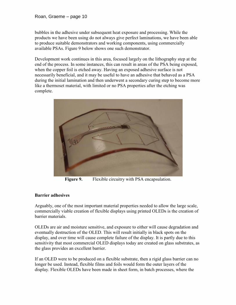
Roan, Graeme – page 10 bubbles in the adhesive under subsequent heat exposure and processing. While the
products we have been using do not always give perfect laminations, we have been able
to produce suitable demonstrators and working components, using commercially
available PSAs. Figure 9 below shows one such demonstrator.
Development work continues in this area, focused largely on the lithography step at the
end of the process. In some instances, this can result in areas of the PSA being exposed,
when the copper foil is etched away. Having an exposed adhesive surface is not
necessarily beneficial, and it may be useful to have an adhesive that behaved as a PSA
during the initial lamination and then underwent a secondary curing step to become more
like a thermoset material, with limited or no PSA properties after the etching was
complete.
Figure 9. Flexible circuitry with PSA encapsulation.
Barrier adhesives
Arguably, one of the most important material properties needed to allow the large scale,
commercially viable creation of flexible displays using printed OLEDs is the creation of
barrier materials.
OLEDs are air and moisture sensitive, and exposure to either will cause degradation and
eventually destruction of the OLED. This will result initially in black spots on the
display, and over time will cause complete failure of the display. It is partly due to this
sensitivity that most commercial OLED displays today are created on glass substrates, as
the glass provides an excellent barrier.
If an OLED were to be produced on a flexible substrate, then a rigid glass barrier can no
longer be used. Instead, flexible films and foils would form the outer layers of the
display. Flexible OLEDs have been made in sheet form, in batch processes, where the

Roan, Graeme – page 11 entire assembly is shrouded in a barrier material after manufacture. Whilst successful in
stabilizing the OLED, this is not practical for a low cost roll-to-roll process. One
alternative is to use existing adhesives to form the OLED laminate, and then encapsulate
the edges of the structure, as shown in Figure 10.
Many of the existing encapsulants are not particularly flexible, and should this structure
suffer any delaminations at the edges, then the entire OLED will fail, as moisture and air
could begin to access the bond lines in the laminate.
Figure 10. Side encapsulation of OLEDs.
Perhaps a better solution would be to create a structure where the adhesive itself had
suitable barrier properties, and side encapsulation was no longer necessary, such as is
shown in Figure 11.
Figure 11. Barrier adhesive on OLED.
This is the direction we have taken in our work – to attempt to create an adhesive that can
bond the layers of the OLED structure together, be chemically compatible with the
OLED, and provide suitable barrier protection to prevent ingress of moisture from the
side of the construction.
Acrylic PSAs are not suited to these applications, as their moisture permeation is much
too high. Instead we turned to polyisobutylene adhesives. These offer both much better
barrier properties than acrylics as well as being non-functional, and so less likely to cause
chemical interactions with the OLEDs.
The low glass transition temperature of polyisobutylene gives it many inherently useful
PSA properties. One disadvantage, however, to many commercially available PIBs is that
their non-functional nature makes it difficult to build shear strength into the adhesive,
which can limit their usefulness in many potential applications.

Roan, Graeme – page 12 Our approach involved using commercially available PIB polymers, in solution, and
formulating them with various functional materials and UV crosslinkers, to enable the
production of a coating that would have the expected barrier properties of a PIB, coupled
with the cohesion needed for the application. As with the polarizer adhesives discussed
earlier, we have been coating from solution and then curing by UV radiation. This gives
us both the coating quality we need, and the rapid cure, which is beneficial in the
application.
The moisture uptake rate of the adhesives we designed was between 60 and 100 ppm
when measured at 23°C and 50% relative humidity with a water diffusivity coefficient of
approximately 0.4 x 10⁻¹²
m2/s under the same conditions. For reference, values for the
diffusivity coefficient of (meth)acrylates are considerably higher – approximately 13.3 x
10-12
m2/s for PMMA, for example
7.
To test the ability of our PSAs to provide barrier properties, we started by using rigid
OLEDs. Ultimately, our goal was to create flexible systems, but the rigid systems would
allow for barrier property evaluation separate from the potential complication of a
flexible system.
Our test configuration used a plate with multiple test sites as shown in Figure 12. The
layout on the plate consists of nine OLEDs, and allowed for testing of three
configurations, with each one tested in triplicate. The configurations used were:
- Adhesive with a getter (top row)
- Adhesive without a getter (middle row) and
- No adhesive or getter (bottom row)
-
The last row acted as a control, to examine the decay of the OLED without any additional
layers or barriers.
The getter is a moisture-absorbing matrix (typically calcium oxide) that absorbs, but does
not release, moisture.
Samples prepared in this way were then subjected to various tests. Firstly, we ran JVL
curves (current density – voltage – luminance) both before and after the application of the
adhesive to the OLED. These data are shown in Figure 13, which indicates no meaningful
change in performance of the OLED before or after the application of the adhesive. This
leads us to conclude that the adhesive is chemically compatible with the OLED and that
the efficiency of the OLED is unaffected by the presence of the adhesive.

Roan, Graeme – page 13
Figure 12. OLED test assembly.
Figure 13. JVL curves.
Testing then continued by aging the assembled OLED plates at 60°C and 90% relative
humidity and examining the samples regularly for the presence of black spots – an
indication of OLED degradation.
Whilst the examination and counting of black spots over time was done using a
microscope connected to a digital analyzer and a computer program, the most striking
results are from a visual inspection of the samples. As Figure 14 shows, the adhesive
provides significant protection the OLED against decay. The bottom row of images
-2 -1 0 1 2 3 4 510
-8
10-7
10-6
10-5
10-4
10-3
10-2
10-1
100
101
102
3B before 3B after
J (
mA
/cm2
)
Voltage (V)
2 3 4 5
0
1
2
3
4
5
Effic
ien
cy (
Cd
/A)
3B before 3B after
Voltage (V)

Roan, Graeme – page 14 shows substantial OLED degradation after 12 days (288 hours), whilst the performance is
markedly better with the adhesive in place (and as expected, even better when a getter is
used).
We do see some degradation of the OLED after 12 days, and obviously this is not
suitable performance for a commercially viable OLED, where the display would be
expected to last for multiple years. It is, however, an impressive start, and on a system
with no edge encapsulation, meaning that the adhesive alone was providing protection on
the side of the assembly.
Figure 14. OLED stability tests.
There is obviously much work still to be done, as we improve our barrier performance
and extend our testing to flexible systems, but we are encouraged by these early results
and remain committed to understanding the adhesive needs of these applications and
developing products that help to realize the commercialization of the technology. Holst
has already produced some demonstration OLED samples, although with very short
lifetimes. By the end of 2012, we intend to have a working demonstrator using our
adhesives that will have a useful working lifetime.
Conclusions
This paper has described some of our initial results in our efforts to understand
technology areas that move beyond many of our traditional applications. We have a lot of
work still to do, but we believe that extending our PSA capabilities into areas such as the
display applications we described here offers exciting possibilities for the future and will
help to grow and improve the applications and markets available to PSA coaters and
users.

Roan, Graeme – page 15
Acknowledgements
The polarizer adhesive work was largely carried out by Dr. John Ouyang at Henkel in the
US and Howard Zhu at Henkel in China, with contributions from many colleagues in the
US, China and Korea. The work on adhesives for flexible electronics was carried out by
Dr. Sonny Liu in the US, Dr. Maria Peter and Dr. Jeroen van den Brand at Holst in the
Netherlands, Dr. Anja Schneider at Henkel in Germany and Dr. Maarten Cauwe at
IMEC/University of Gent in Belgium.
References
1. K-H Kim and J-K Son, NPG Nature Asia, 2009, 1, 29-36.
2. Data from DisplaySearch.
3. Y Mori, K Tanahashi and S Tsuji, Opt. Eng., 2004, 43, 2696-2700.
D-M Tsai and H-Y Tsai, Machine Vision & Applications, 2011, 22, 629-649.
4. G A Roan, Y Liu, Z Hu, S C Thompson and P D Palasz, Pressure Sensitive Tape
Council TECH XXX, 2007, 171-183.
G A Roan, Y Liu, D S Bull and P D Palasz, Proceedings of the 30th
Annual
Meeting of the Adhesion Society, 2007, 312-314.
5. Data from IDTechEx.
6. More information about Holst Centre can be found at www.holstcentre.com
7. M Unemori, Y Matsuya, S Matsuya, A Akashi and A Akamino, Biomaterials,
2003, 24, 1381-1387.