discover the secrets of the nanoworld h - zsi
TRANSCRIPT
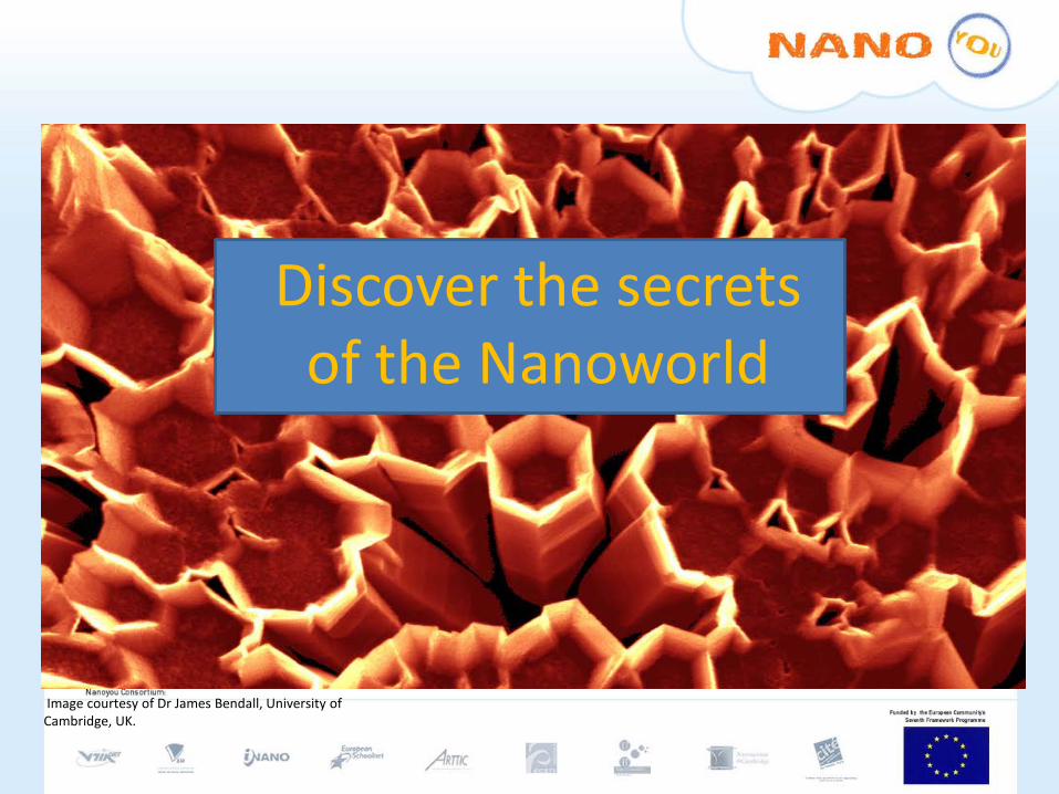
hDiscover the secrets
of the Nanoworld
Image courtesy of Dr James Bendall, University of Cambridge, UK.
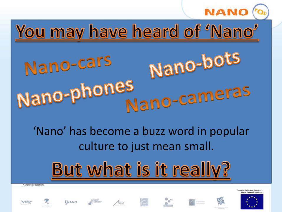
‘Nano’ has become a buzz word in popular culture to just mean small.
To understand nanotechnology we must first think about scale.
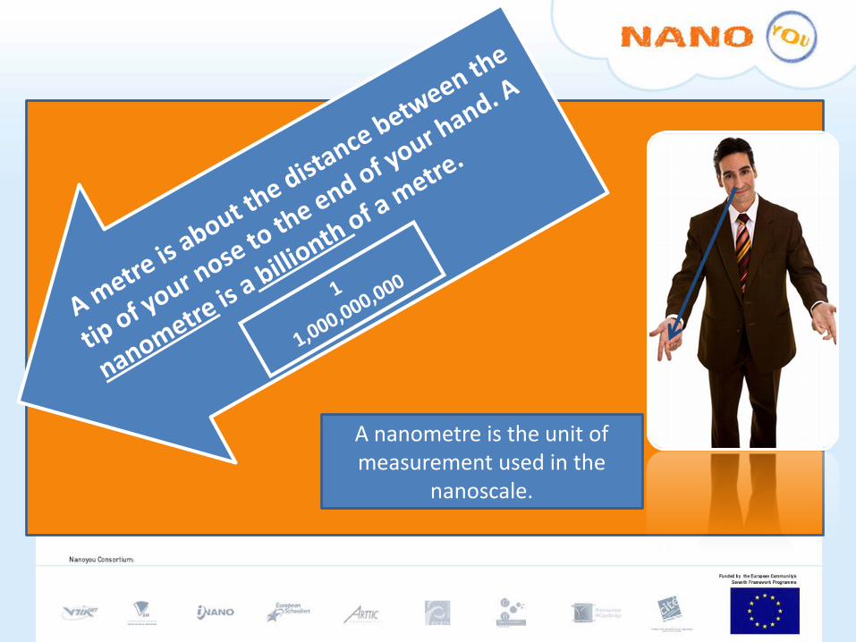
A nanometre is the unit of measurement used in the
nanoscale.
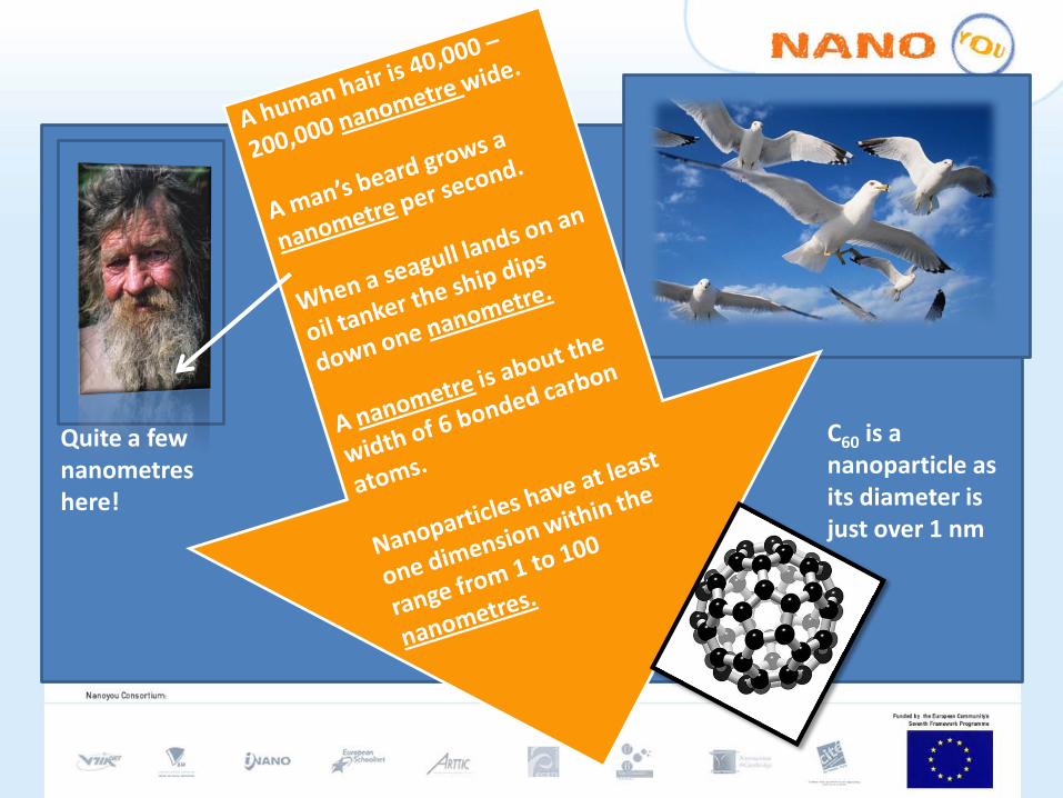
Quite a few nanometres here!
C60 is a nanoparticle as its diameter is just over 1 nm
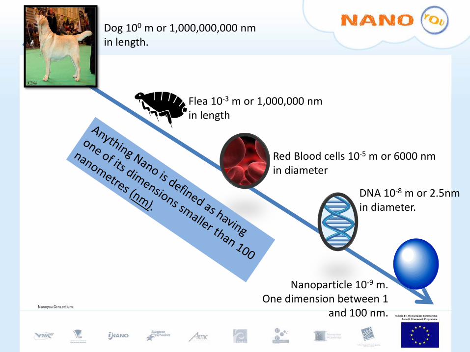
Flea 10-3 m or 1,000,000 nm in length
Red Blood cells 10-5 m or 6000 nm in diameter
DNA 10-8 m or 2.5nm in diameter.
Nanoparticle 10-9 m.One dimension between 1
and 100 nm.
Dog 100 m or 1,000,000,000 nm in length.
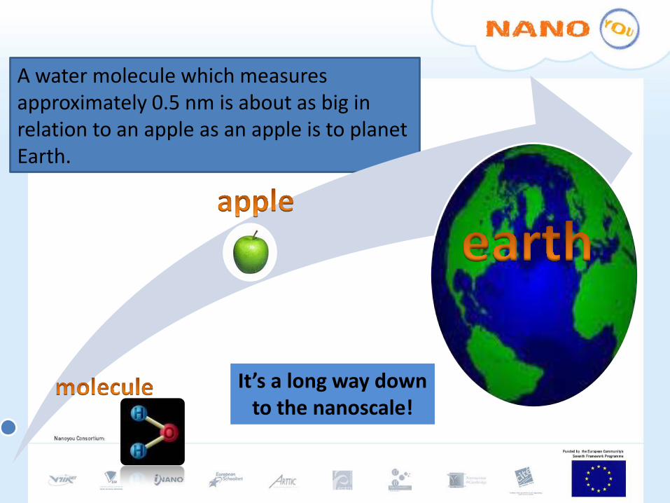
A water molecule which measures approximately 0.5 nm is about as big in relation to an apple as an apple is to planet Earth.
It’s a long way down to the nanoscale!
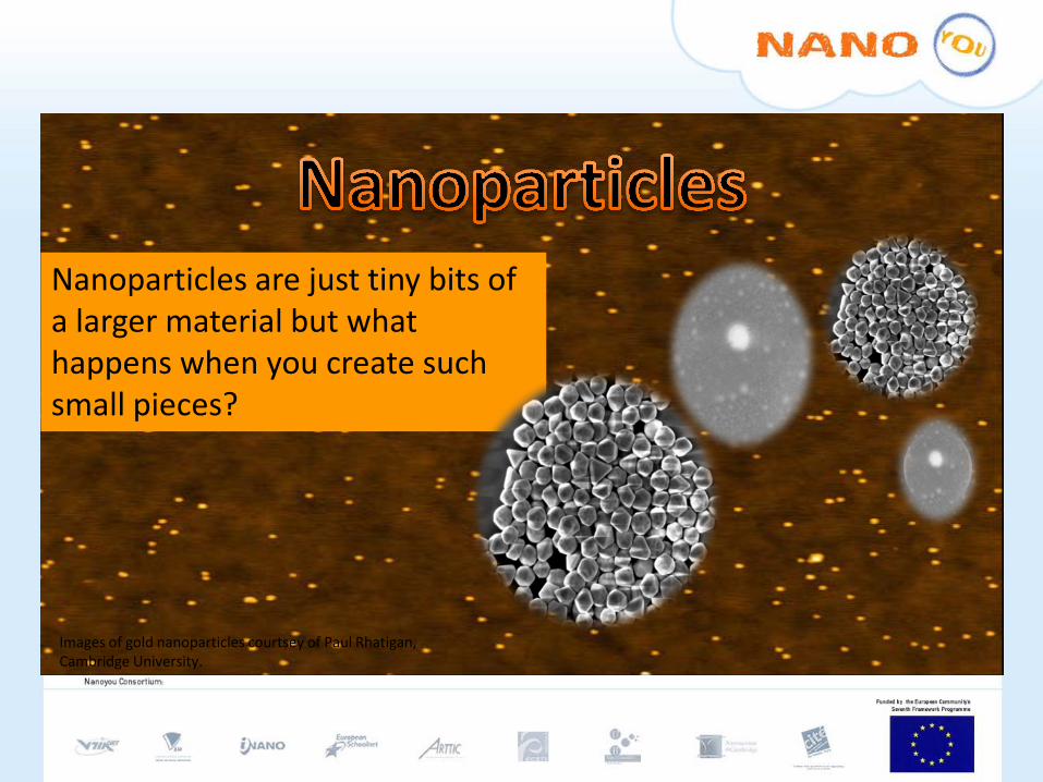
Nanoparticles are just tiny bits of a larger material but what happens when you create such small pieces?
Images of gold nanoparticles courtsey of Paul Rhatigan, Cambridge University.
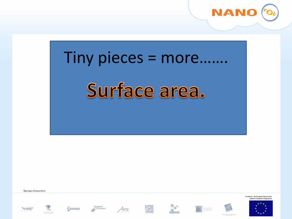
Tiny pieces = more…….
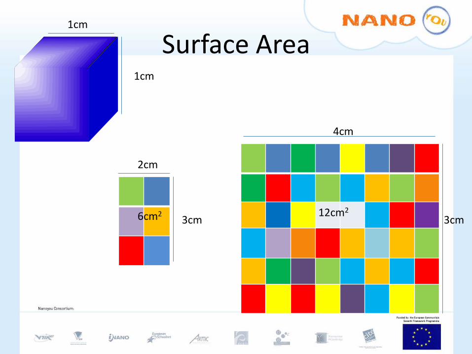
Surface Area
4cm
3cm12cm2
2cm
3cm6cm2
1cm
1cm

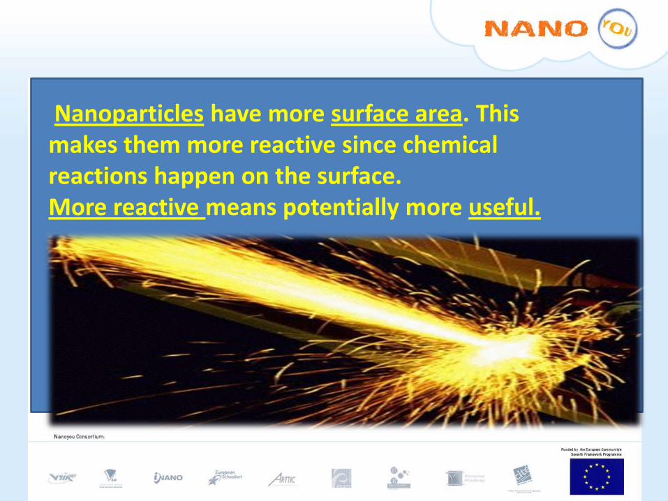
Nanoparticles have more surface area. This makes them more reactive since chemical reactions happen on the surface.More reactive means potentially more useful.
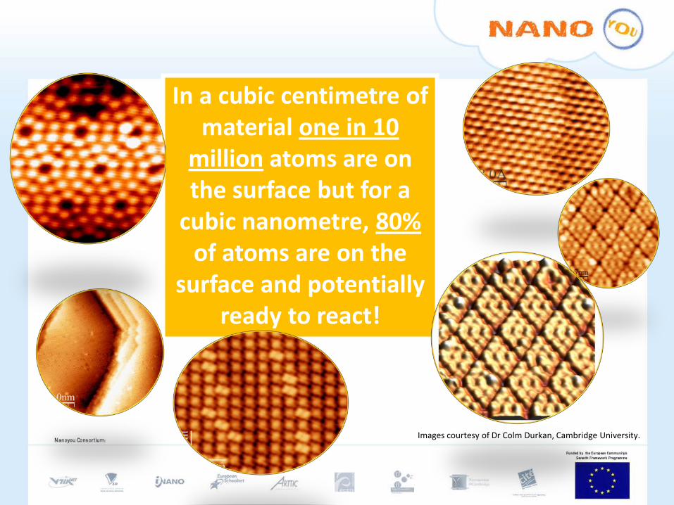
In a cubic centimetre of material one in 10
million atoms are on the surface but for a
cubic nanometre, 80% of atoms are on the
surface and potentially ready to react!
Images courtesy of Dr Colm Durkan, Cambridge University.
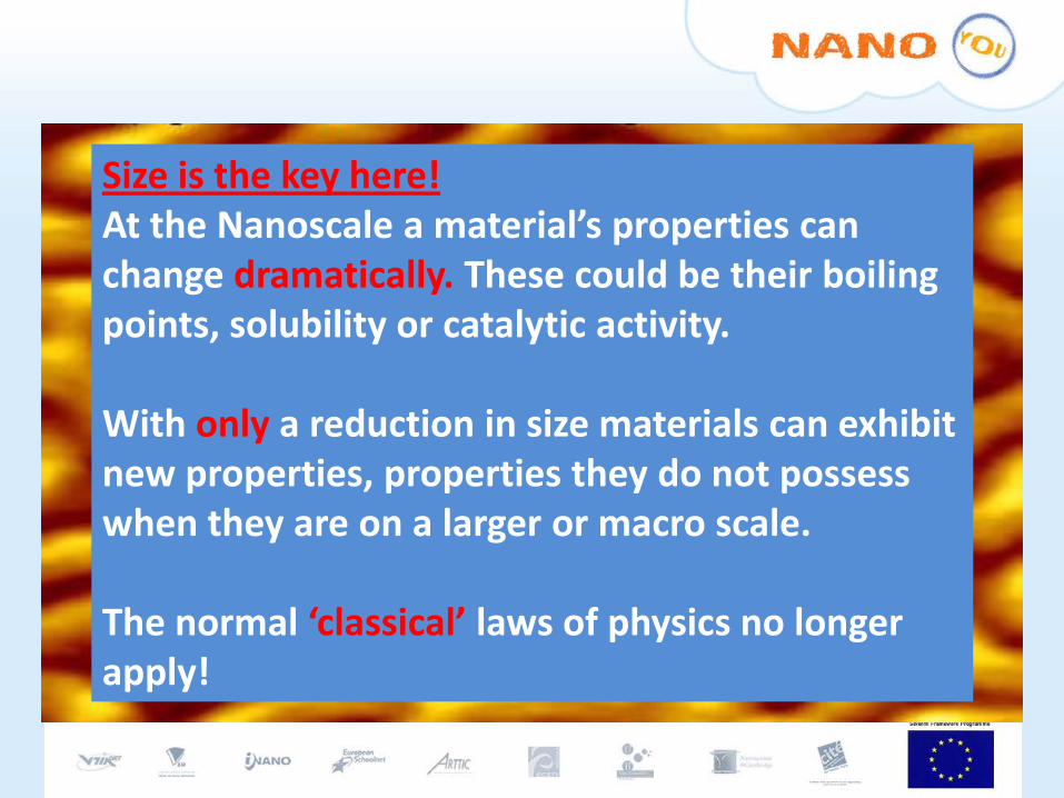
Size is the key here! At the Nanoscale a material’s properties can change dramatically. These could be their boiling points, solubility or catalytic activity.
With only a reduction in size materials can exhibit new properties, properties they do not possess when they are on a larger or macro scale.
The normal ‘classical’ laws of physics no longer apply!
MACRO
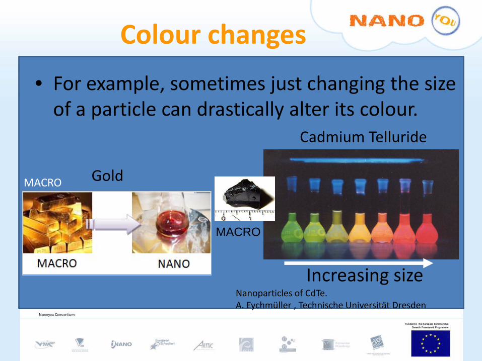
• For example, sometimes just changing the size of a particle can drastically alter its colour.
Colour changes
Increasing size
Cadmium Telluride
Nanoparticles of CdTe.A. Eychmüller , Technische Universität Dresden
Gold
MACRO
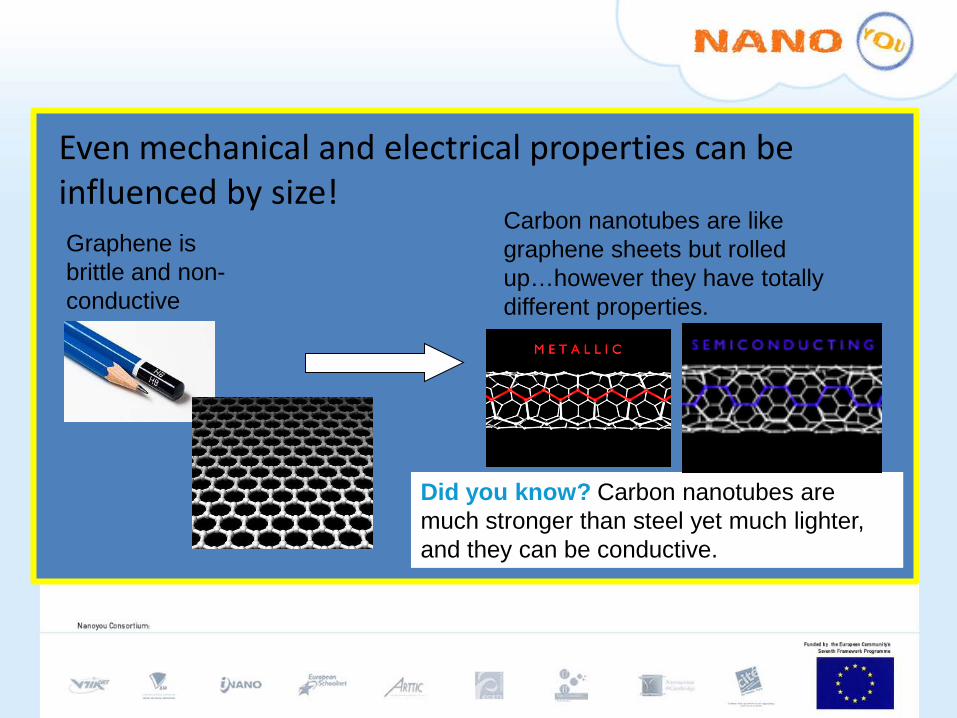
Even mechanical and electrical properties can be influenced by size!Graphene is brittle and non-conductive
Carbon nanotubes are like graphene sheets but rolled up…however they have totally different properties.
Did you know? Carbon nanotubes are much stronger than steel yet much lighter, and they can be conductive.

So how do scientists work on such a tiny scale?

Mainly because microscopes have become more sophisticated.
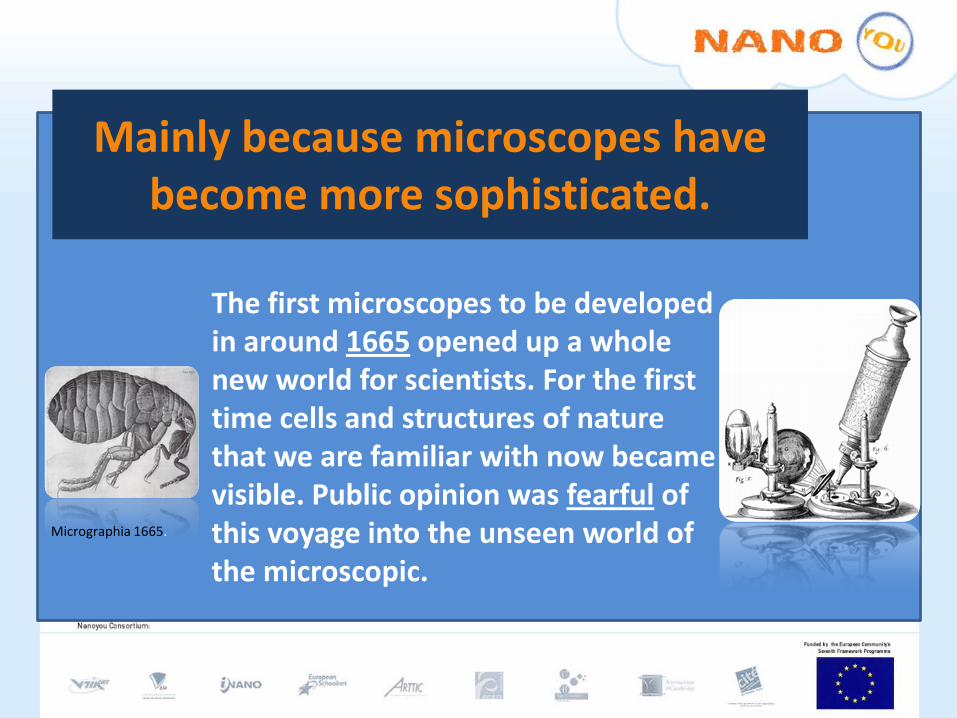
The first microscopes to be developed in around 1665 opened up a whole new world for scientists. For the first time cells and structures of nature that we are familiar with now became visible. Public opinion was fearful of this voyage into the unseen world of the microscopic.
Micrographia 1665.
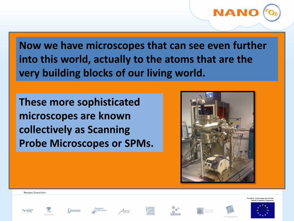
Now we have microscopes that can see even further into this world, actually to the atoms that are the very building blocks of our living world.
These more sophisticated microscopes are known collectively as Scanning Probe Microscopes or SPMs.
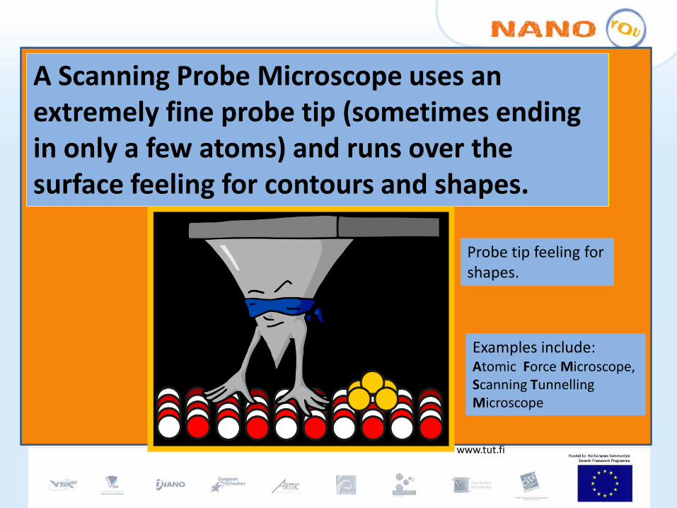
A Scanning Probe Microscope uses an extremely fine probe tip (sometimes ending in only a few atoms) and runs over the surface feeling for contours and shapes.
www.tut.fi
Probe tip feeling for shapes.
Examples include:Atomic Force Microscope,Scanning Tunnelling Microscope
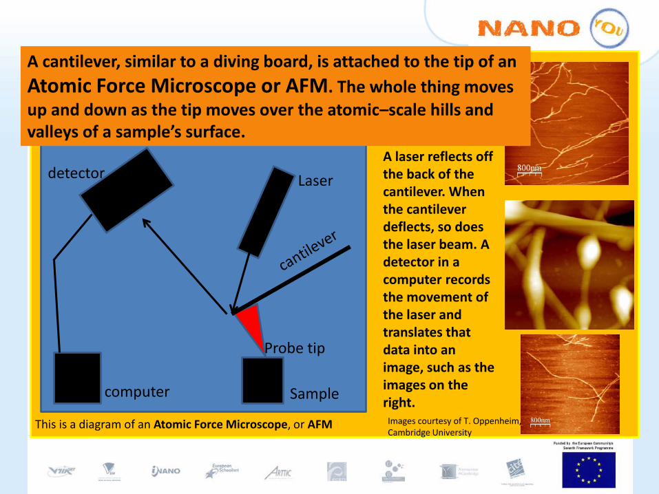
A laser reflects off the back of the cantilever. When the cantilever deflects, so does the laser beam. A detector in a computer records the movement of the laser and translates that data into an image, such as the images on the right.
Laserdetector
computer Sample
Probe tip
This is a diagram of an Atomic Force Microscope, or AFM Images courtesy of T. Oppenheim, Cambridge University
A cantilever, similar to a diving board, is attached to the tip of an Atomic Force Microscope or AFM. The whole thing moves up and down as the tip moves over the atomic–scale hills and valleys of a sample’s surface.

Scanning tunnelling microscope.
Images courtesy of Cambridge university, Nanoscience Centre.
A scanning tunnelling microscope works by having a tiny probe which scans across a surface picking up variations in the current that runs between itself and the atoms on the surface. This probe is made of conducting material (usually Tungsten) and the very end of it is only 1 atom wide!
A tungsten tip for STM imaging.
These variations in current are translated into images such as the ones to the right.
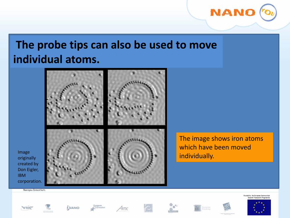
The probe tips can also be used to move individual atoms.
The image shows iron atoms which have been moved individually.
Image originally created by Don Eigler, IBM corporation.

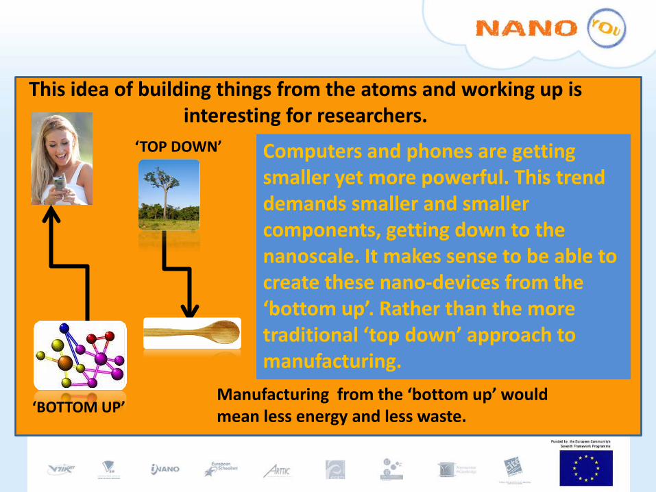
This idea of building things from the atoms and working up is interesting for researchers.
Computers and phones are getting smaller yet more powerful. This trend demands smaller and smaller components, getting down to the nanoscale. It makes sense to be able to create these nano-devices from the ‘bottom up’. Rather than the more traditional ‘top down’ approach to manufacturing.
Manufacturing from the ‘bottom up’ would mean less energy and less waste.‘BOTTOM UP’
‘TOP DOWN’

Moving atoms individually is still not a viable technique for creating nanostructures because it’s too slow. However there is another process called ‘SELF ASSEMBLY’, often seen in nature,which scientists can exploit.
Atoms, molecules or nanoparticles will arrange themselves into larger structures if they have the right properties and environments. This process plays a central role in the construction of DNA, cells, bones and viruses. These all self assemble without assistance.
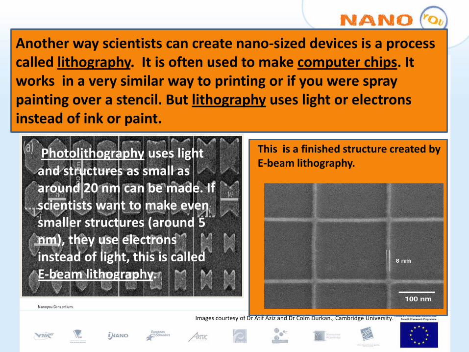
Another way scientists can create nano-sized devices is a process called lithography. It is often used to make computer chips. It works in a very similar way to printing or if you were spray painting over a stencil. But lithography uses light or electrons instead of ink or paint.
This is a finished structure created by E-beam lithography.
Photolithography uses light and structures as small as around 20 nm can be made. If scientists want to make even smaller structures (around 5 nm), they use electrons instead of light, this is called E-beam lithography.
Images courtesy of Dr Atif Aziz and Dr Colm Durkan., Cambridge University.
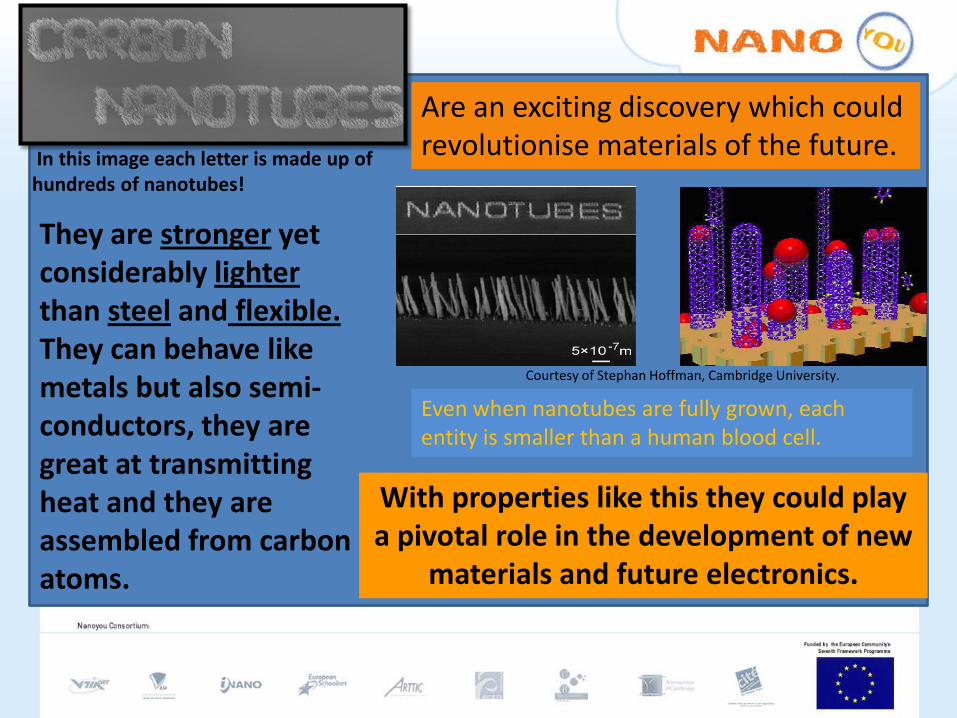
They are stronger yet considerably lighterthan steel and flexible. They can behave like metals but also semi-conductors, they are great at transmitting heat and they are assembled from carbon atoms.
With properties like this they could play a pivotal role in the development of new
materials and future electronics.
In this image each letter is made up of hundreds of nanotubes!
Even when nanotubes are fully grown, each entity is smaller than a human blood cell.
Are an exciting discovery which could revolutionise materials of the future.
Courtesy of Stephan Hoffman, Cambridge University.
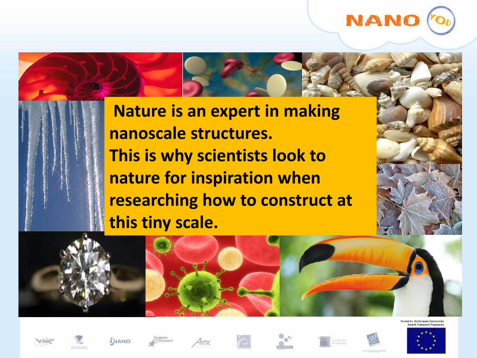
Nature is an expert in making nanoscale structures.This is why scientists look to nature for inspiration when researching how to construct at this tiny scale.
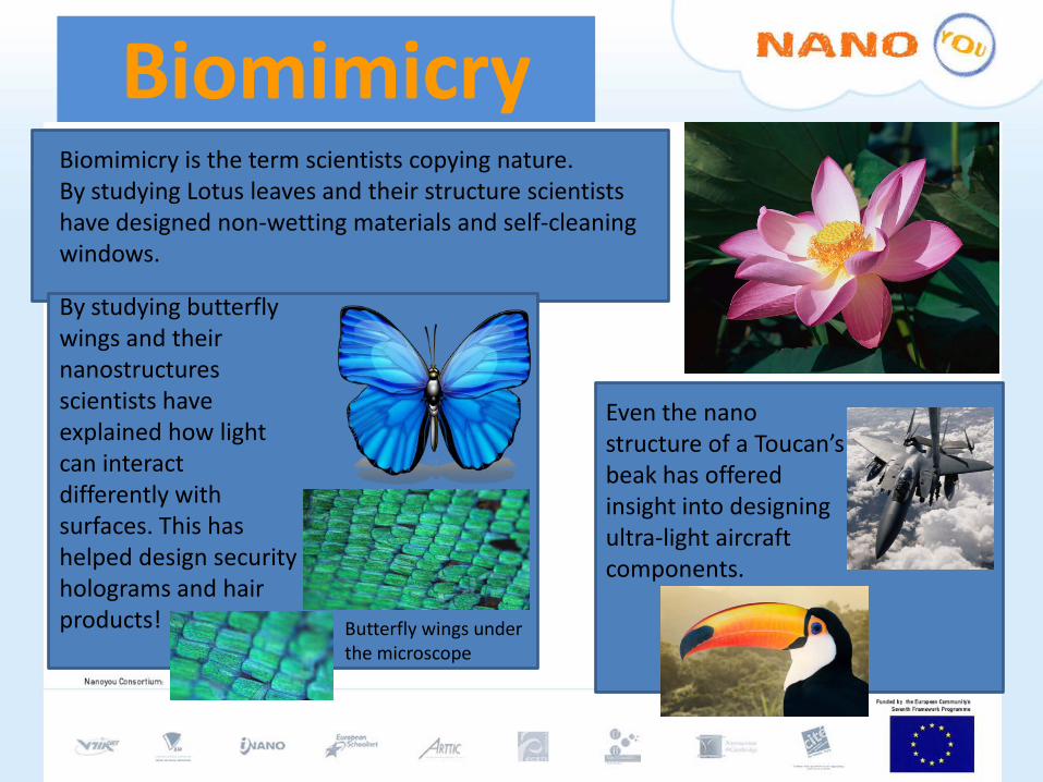
BiomimicryBiomimicry is the term scientists copying nature. By studying Lotus leaves and their structure scientists have designed non-wetting materials and self-cleaning windows.
By studying butterfly wings and their nanostructures scientists have explained how light can interact differently with surfaces. This has helped design security holograms and hair products!
Even the nano structure of a Toucan’s beak has offered insight into designing ultra-light aircraft components.
Butterfly wings under the microscope
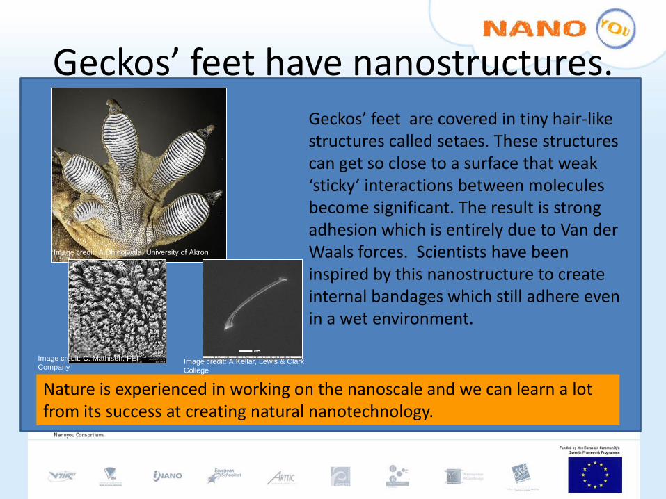
Geckos’ feet have nanostructures.Geckos’ feet are covered in tiny hair-like structures called setaes. These structures can get so close to a surface that weak ‘sticky’ interactions between molecules become significant. The result is strong adhesion which is entirely due to Van der Waals forces. Scientists have been inspired by this nanostructure to create internal bandages which still adhere even in a wet environment.
Nature is experienced in working on the nanoscale and we can learn a lot from its success at creating natural nanotechnology.
Image credit: A.Dhinojwala, University of Akron
Image credit: C. Mathisen, FEI Company
Image credit: A.Kellar, Lewis & Clark College

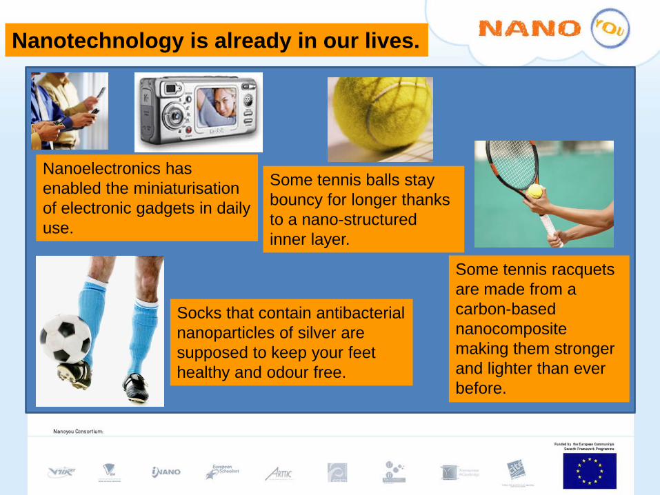
Nanotechnology is already in our lives.
Nanoelectronics has enabled the miniaturisation of electronic gadgets in daily use.
Some tennis balls stay bouncy for longer thanks to a nano-structured inner layer.
Some tennis racquets are made from a carbon-based nanocomposite making them stronger and lighter than ever before.
Socks that contain antibacterial nanoparticles of silver are supposed to keep your feet healthy and odour free.
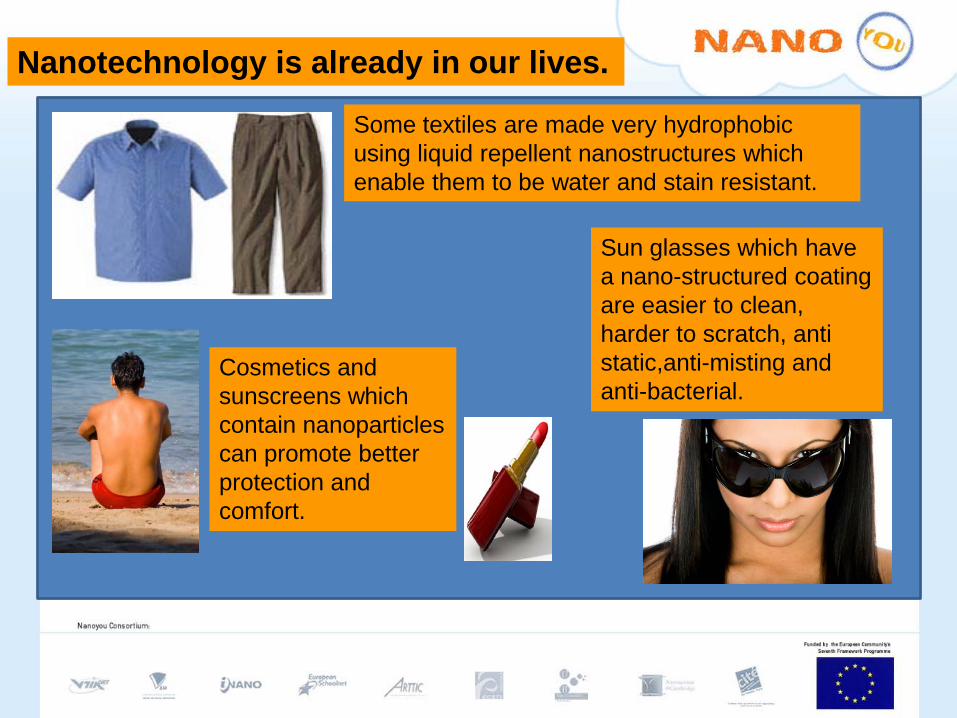
Some textiles are made very hydrophobic using liquid repellent nanostructures which enable them to be water and stain resistant.
Cosmetics and sunscreens which contain nanoparticles can promote better protection and comfort.
Sun glasses which have a nano-structured coating are easier to clean, harder to scratch, anti static,anti-misting and anti-bacterial.
Nanotechnology is already in our lives.

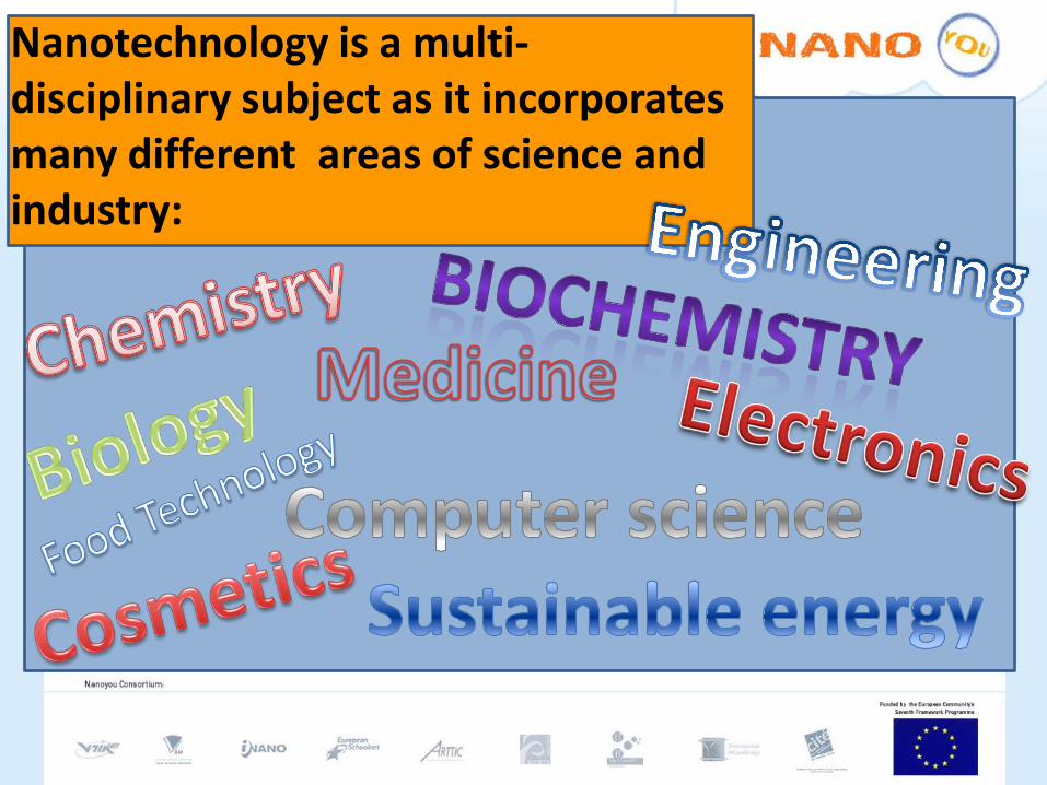
Nanotechnology is a multi-disciplinary subject as it incorporates many different areas of science and industry:
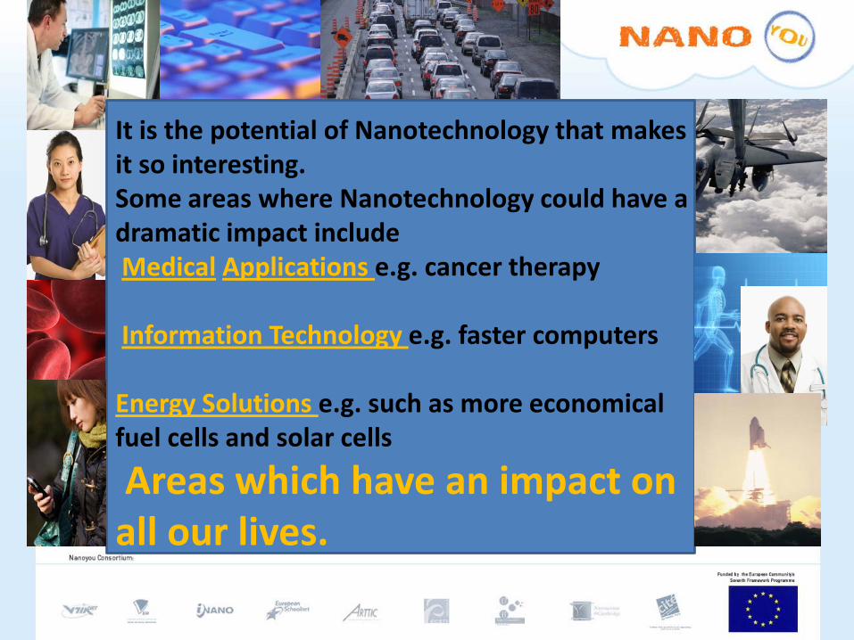
It is the potential of Nanotechnology that makes it so interesting.Some areas where Nanotechnology could have a dramatic impact includeMedical Applications e.g. cancer therapy
Information Technology e.g. faster computers
Energy Solutions e.g. such as more economical fuel cells and solar cells
Areas which have an impact on all our lives.

www.nanoyou.eu