digitaltranceiver v5 9.ppt - ieee of fm modulation • commercial fm radio broadcasts at 88mhz to...
TRANSCRIPT
��������������� �������������������� ������ � � � ����� ��� �� � ����� ��� ��� �� � � � ����� ��� �� � ����� ��� ��� �
� � � �� � � �
������������� � �� �� ��� ���� �� �� � �� ����� � �� �� ��� ���� �� �� � �� ��� � ���� �� � � � �� � �! " #�$ % % "� � ���� �� � � � �� � �! " #�$ % % "
David Farrell
rev 1
Dane SpristerMatthew Taylor
Colorado Electronic Product Design, Inc.

TopicsTopics
• Introduction• Abstract• System Block Diagram• Up/Down Conversion• Modulation• Modulation• Demodulation• Demonstration System• Questions
� 2009 by CEPD, Inc. www.cepd.com
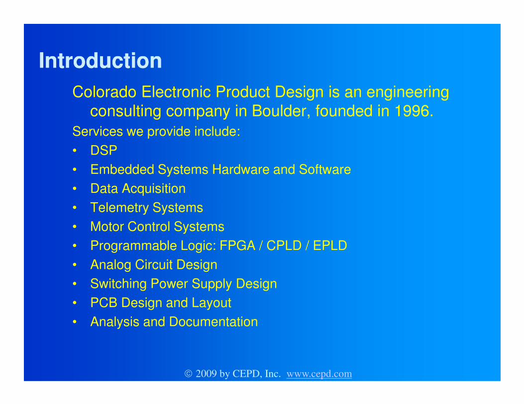
IntroductionIntroductionColorado Electronic Product Design is an engineering
consulting company in Boulder, founded in 1996.Services we provide include:• DSP • Embedded Systems Hardware and Software • Data Acquisition • Telemetry Systems • Telemetry Systems • Motor Control Systems • Programmable Logic: FPGA / CPLD / EPLD • Analog Circuit Design • Switching Power Supply Design • PCB Design and Layout • Analysis and Documentation
� 2009 by CEPD, Inc. www.cepd.com

AbstractAbstractThis presentation by Colorado Electronic
Product Design explores an FPGA based configurable digital radio, and demonstrates an FM transceiver design. The trend in software radios is moving toward an all-digital design within a single chip. Most elements of design within a single chip. Most elements of a digital radio can now be implemented within an FPGA. A high-speed analog to digital converter board and an FPGA board are used to implement a working radio using VHDL.
� 2009 by CEPD, Inc. www.cepd.com
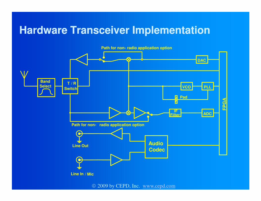
Hardware Transceiver ImplementationHardware Transceiver Implementation
T / R Switch
Pad
VCO PLLBand Select
DAC
FPG
A
Path for non- radio application option
IF Filter ADC
FPG
A
Path for non- radio application option
Line Out
Line In / Mic
Audio Codec
� 2009 by CEPD, Inc. www.cepd.com
The platform is fairly flexibleThe platform is fairly flexible
• The impedance of the PCB signal paths are wideband and 50 ohm
• Mixers, which can be bypassed, are provided for up/down conversion
• Key components are socket-ed, different • Key components are socket-ed, different bands can be targeted by changing out filters, etc.
• The ADC and DAC support over 200 MSPS• The main signal processing algorithms are
performed by a configurable FPGA
� 2009 by CEPD, Inc. www.cepd.com
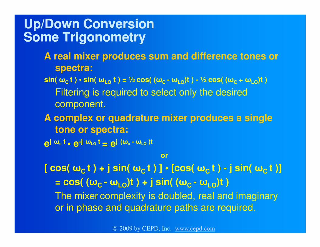
Up/Down Conversion Up/Down Conversion Some TrigonometrySome Trigonometry
A real mixer produces sum and difference tones or spectra:
sin( �C t ) • sin( �LO t ) = ½ cos( (�C - �LO)t ) - ½ cos( (�C + �LO)t )
Filtering is required to select only the desired component.
A complex or quadrature mixer produces a single tone or spectra:
ej �c t • e-j �LO t = ej (�c - �LO )t
or
[ cos( �C t ) + j sin( �C t ) ] • [cos( �C t ) - j sin( �C t )] = cos( (�C - �LO)t ) + j sin( (�C - �LO)t )The mixer complexity is doubled, real and imaginary or in phase and quadrature paths are required.
� 2009 by CEPD, Inc. www.cepd.com
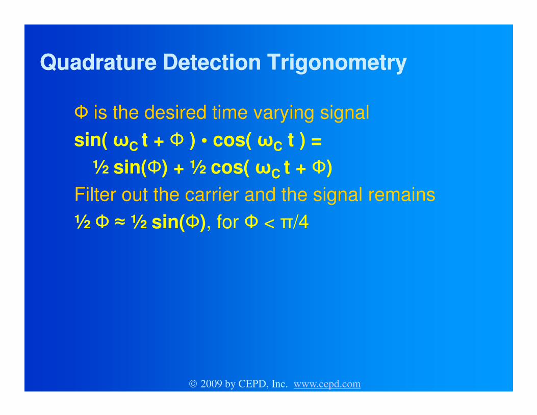
QuadratureQuadrature Detection TrigonometryDetection Trigonometry
� is the desired time varying signalsin( �C t + � ) • cos( �C t ) =
½ sin(�) + ½ cos( �C t + �)Filter out the carrier and the signal remains½ � � ½ sin(�), for � < �/4
� 2009 by CEPD, Inc. www.cepd.com

Real Down Conversion Real Down Conversion –– Moving the Moving the carrier to the IFcarrier to the IF
– The mixed signal contains two frequencies:
– Mixing the carrier with a real local oscillator
– The mixed signal contains two frequencies:• �C - �LO and �C + �LO
– If the local oscillator frequency is chosen to be �C – �IF,the two resultant frequencies are: �IF and 2 �C - �IF
� 2009 by CEPD, Inc. www.cepd.com
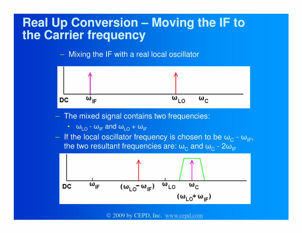
Real Up Conversion Real Up Conversion –– Moving the IF to Moving the IF to the Carrier frequencythe Carrier frequency
– The mixed signal contains two frequencies:
– Mixing the IF with a real local oscillator
– The mixed signal contains two frequencies:• �LO - �IF and �LO + �IF
– If the local oscillator frequency is chosen to be �C - �IF,the two resultant frequencies are: �C and �C - 2�IF
� 2009 by CEPD, Inc. www.cepd.com
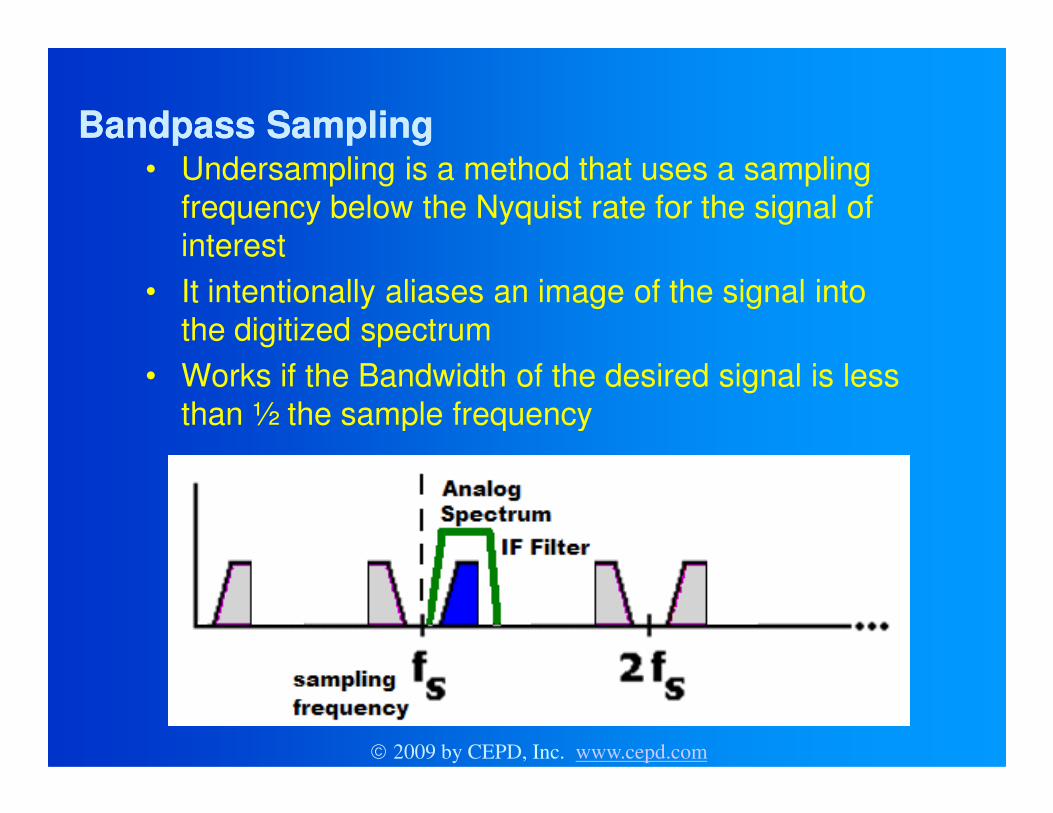
BandpassBandpass SamplingSampling• Undersampling is a method that uses a sampling
frequency below the Nyquist rate for the signal of interest
• It intentionally aliases an image of the signal into the digitized spectrum
• Works if the Bandwidth of the desired signal is less than ½ the sample frequencythan ½ the sample frequency
� 2009 by CEPD, Inc. www.cepd.com

FM ModulationFM Modulation
� 2009 by CEPD, Inc. www.cepd.com
PurposePurpose
The purpose of this section is to:• Present algorithms for implementation of an
FPGA controlled FM modulator.• Present a hardware platform that can be used to
implement the design of different modulation implement the design of different modulation implementations.
� 2009 by CEPD, Inc. www.cepd.com
Outline of this sectionOutline of this section
• Overview of FM Radio and FM Radio sub carriers
• Outline of Direct Digital Synthesis Architecture• Implementation of Modulator Reference design• Overview of the Analog Board• Overview of the Analog Board
� 2009 by CEPD, Inc. www.cepd.com

Overview of FM ModulationOverview of FM Modulation
• Commercial FM radio broadcasts at 88MHz to 108MHz• There is a separation of 200kHz between adjacent stations.• The peak frequency deviation is 75kHz.• The left and right channels are added and subtracted to generate
L+R and L-R.• The L+R (monophonic) and L-R (stereo) signals are preemphasized.• The L-R signal is modulated and added to the L+R and 19kHz pilot • The L-R signal is modulated and added to the L+R and 19kHz pilot
signal prior to the FM modulator block.
� 2009 by CEPD, Inc. www.cepd.com

Implementing FM Modulator in VHDLImplementing FM Modulator in VHDL
• Signal to be transmitted is a monophonic signal. – Left and right channels are not present, so they do
not need to be added and subtracted to get L+R and L-R.
– Because left and right channels are not both present a 19kHz pilot is not required. a 19kHz pilot is not required.
• Preemphasis is not used.• The input audio signal is not DSB-SC for a
38KHz carrier (because there is no pilot signal).
� 2009 by CEPD, Inc. www.cepd.com
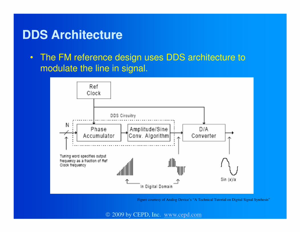
DDS ArchitectureDDS Architecture
• The FM reference design uses DDS architecture to modulate the line in signal.
Figure courtesy of Analog Device’s “A Technical Tutorial on Digital Signal Synthesis”
� 2009 by CEPD, Inc. www.cepd.com

Overview of DDS ArchitectureOverview of DDS Architecture
• The phase accumulator:– Tracks the phase of the sine wave.– Uses a modulus n counter to allow the sine wave frequency to
change quickly using a tuning word.– Is incremented every system clock cycle by the value of the
tuning word.
Figure courtesy of Analog Device’s “A Technical Tutorial on Digital Signal Synthesis”
� 2009 by CEPD, Inc. www.cepd.com

Overview of DDS ArchitectureOverview of DDS Architecture
• The output of the phase accumulator is connected to a phase to amplitude converter.– The value of the phase accumulator is truncated and mapped to
a sine wave lookup table.– Without phase accumulator truncation, the amount of memory
required for the lookup table is too large.
� 2009 by CEPD, Inc. www.cepd.com
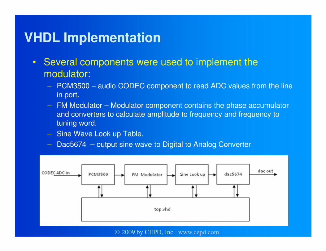
VHDL ImplementationVHDL Implementation
• Several components were used to implement the modulator:– PCM3500 – audio CODEC component to read ADC values from the line
in port.– FM Modulator – Modulator component contains the phase accumulator
and converters to calculate amplitude to frequency and frequency to tuning word.tuning word.
– Sine Wave Look up Table.– Dac5674 – output sine wave to Digital to Analog Converter
� 2009 by CEPD, Inc. www.cepd.com

PCM3500PCM3500
• This component interfaces with the PCM3500 16-bit audio CODEC.
• This component shifts the 16-bit ADC value from the audio CODEC serially and stores the value in a 16-bit register.
� 2009 by CEPD, Inc. www.cepd.com

FM ModulatorFM Modulator
• The audio CODEC value is converted from 2’s compliment to a binary offset value.
• The value is then converted from an amplitude to a frequency.
• The frequency is converted to a tuning word value. • The values used for conversions are Q16, so the values • The values used for conversions are Q16, so the values
are converted back to Q0 values by shifting the values.• The tuning word is added to a pre-calculated tuning word
for 10.625MHz.• The tuning word is added to the value in the phase
accumulator (this tuning word is added to the phase accumulator every system clock cycle).
• The phase accumulator value is output to the top.vhd level.
� 2009 by CEPD, Inc. www.cepd.com
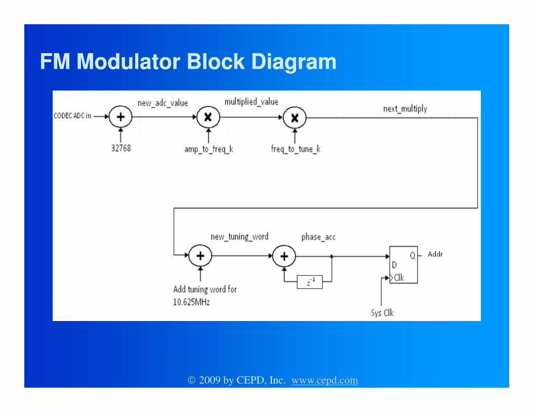
FM Modulator Block DiagramFM Modulator Block Diagram
� 2009 by CEPD, Inc. www.cepd.com
Sine Wave LookSine Wave Look--up Tableup Table
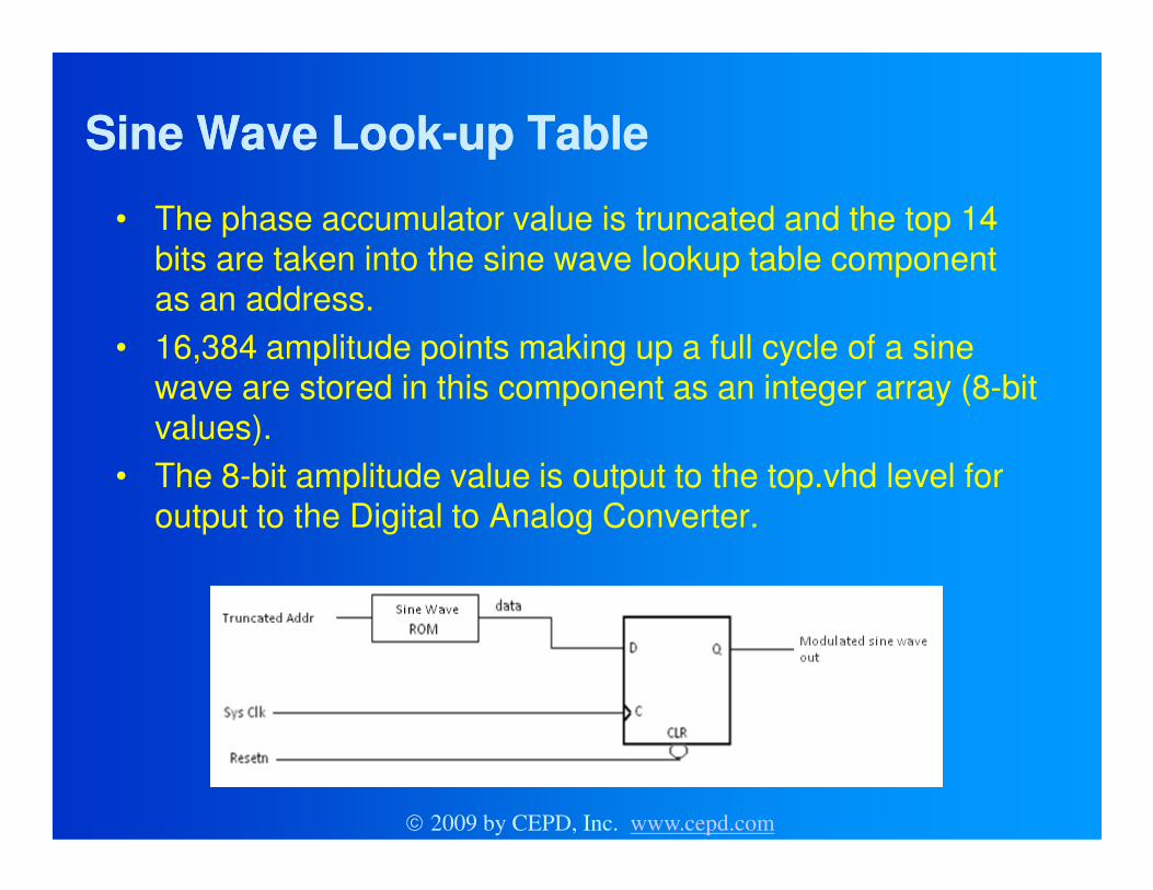
• The phase accumulator value is truncated and the top 14 bits are taken into the sine wave lookup table component as an address.
• 16,384 amplitude points making up a full cycle of a sine wave are stored in this component as an integer array (8-bit values).values).
• The 8-bit amplitude value is output to the top.vhd level for output to the Digital to Analog Converter.
� 2009 by CEPD, Inc. www.cepd.com

dac5674dac5674
• The 8-bit amplitude value from the sine wave lookup table is placed in an output register in the top.vhd level (placed in the top 8-bits of the 14-bit DAC output register).
• The output register is mapped to the dac5674 component.component.
• The 14-bit output register is clocked out to the DAC and, if the Transmit/Receive switch is depressed, transmitted.
� 2009 by CEPD, Inc. www.cepd.com
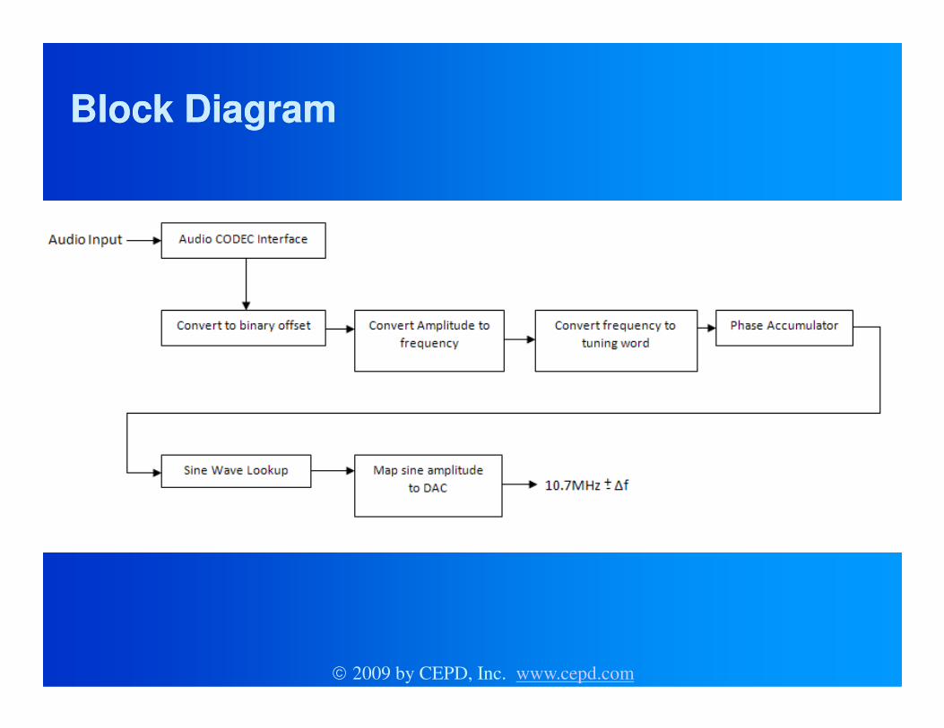
Block DiagramBlock Diagram
� 2009 by CEPD, Inc. www.cepd.com
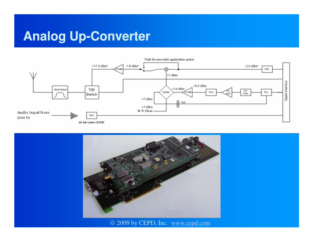
Analog UpAnalog Up--ConverterConverter
� 2009 by CEPD, Inc. www.cepd.com

��������� � ��� � ������������� � ��� � ����
Through Quadrature Detection
� 2009 by CEPD, Inc. www.cepd.com
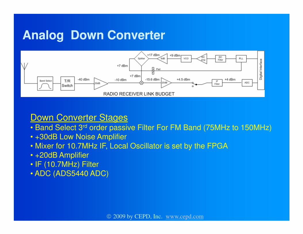
Analog Down Converter Analog Down Converter
Down Converter Stages Down Converter Stages • Band Select 3rd order passive Filter For FM Band (75MHz to 150MHz)• +30dB Low Noise Amplifier• Mixer for 10.7MHz IF, Local Oscillator is set by the FPGA• +20dB Amplifier• IF (10.7MHz) Filter• ADC (ADS5440 ADC)
� 2009 by CEPD, Inc. www.cepd.com

FPGA Demodulation Block DiagramFPGA Demodulation Block Diagram
•Sample ADC at 66.5MHz• Limiter• Down Sample to 8.3125MHz• Demodulate• Down Sample to 24KHz• Parallel to Serial data conversion• 24KHz write to CODEC
� 2009 by CEPD, Inc. www.cepd.com
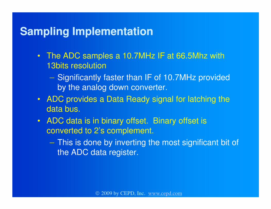
Sampling ImplementationSampling Implementation
• The ADC samples a 10.7MHz IF at 66.5Mhz with 13bits resolution– Significantly faster than IF of 10.7MHz provided
by the analog down converter.• ADC provides a Data Ready signal for latching the
data bus.data bus.• ADC data is in binary offset. Binary offset is
converted to 2’s complement.– This is done by inverting the most significant bit of
the ADC data register.
� 2009 by CEPD, Inc. www.cepd.com
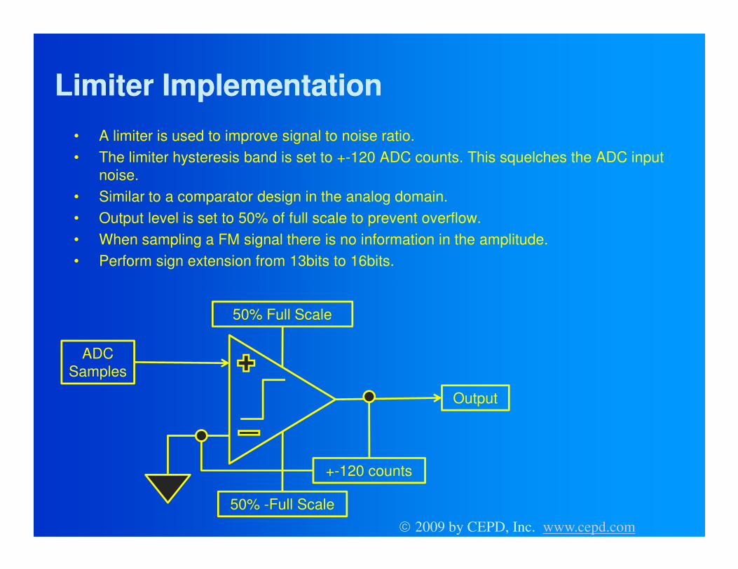
Limiter ImplementationLimiter Implementation• A limiter is used to improve signal to noise ratio.• The limiter hysteresis band is set to +-120 ADC counts. This squelches the ADC input
noise.• Similar to a comparator design in the analog domain.• Output level is set to 50% of full scale to prevent overflow.• When sampling a FM signal there is no information in the amplitude.• Perform sign extension from 13bits to 16bits.
ADC Samples
+-120 counts
50% Full Scale
50% -Full Scale
Output
� 2009 by CEPD, Inc. www.cepd.com

Down SampleDown Sample
• The 66.5MHz sample frequency is then down sampled to create a 8.3125MHz IF.– Latch every 8th sample
• The IF frequency of 10.7 MHz is sampled at 8.3125 MHz, producing a flipped image at 5.925 MHz and a positive image at 2.3875 MHz. positive image at 2.3875 MHz.
• A center frequency of 2.3875Mhz will be chosen for the band pass filter, removing the 5.925Mhz reflection.
10.75.925 8.31252.3875 4.156250� 2009 by CEPD, Inc. www.cepd.com

FM Demodulator StagesFM Demodulator Stages
Hilbert Transform Biquad Bandpass Filter Low Pass Filter
Fs = 8.3125MHz Fs = 8.3125MHz Fs = 8.3125MHz
Fc = 2.3875MHz Fc = 12KHz
BW = +-75KHz
� 2009 by CEPD, Inc. www.cepd.com

FM FM QuadratureQuadrature DemodulatorDemodulator
# Description Signal Processing
1 Input Signal sin(2� f t)
Φ = Φ(f(t) + �f)
1 Input Signal sin(2� fIF t)
2 Hilbert TransformQ = �/2 phase shift
I = sin(2� fIF t)Q =cos(2� fIF t)
3 Band Pass Filter Q2 = cos(2� fIF t + Φ)
4 Multiplier I*Q2 sin(2� fIF t) cos(2� fIF t + Φ )
5 Product to Sum Trig. Identity ½ sin (-Φ (f)) + ½ sin(4� fIF t + Φ)
6 Low Pass Filter ½ sin (-Φ)
7 Recovered Base Band Output
½ sin (-Φ) � ½ -Φ
� 2009 by CEPD, Inc. www.cepd.com

22ndnd Order FIR used for the Order FIR used for the ππππππππ / 2 phase shift (Hilbert Transform)/ 2 phase shift (Hilbert Transform)
Z-1
Z-1
b2b1b0
input
+output
Y N_ _ = ���� bk •••• z-k
k=0 X
� 2009 by CEPD, Inc. www.cepd.com

Hilbert Transform ResponseHilbert Transform Response
� 2009 by CEPD, Inc. www.cepd.com

22ndnd Order IIR Biquad used for theOrder IIR Biquad used for theBandpass FilterBandpass Filter
Z-1
input
Z-1
+
b0
-a1 b1
+
+
+
+
+
output
b2+ -a2 +
N���� bk •••• z-k
Y k=0 ___ = ____________
X N���� ak •••• z-k
k=0
� 2009 by CEPD, Inc. www.cepd.com
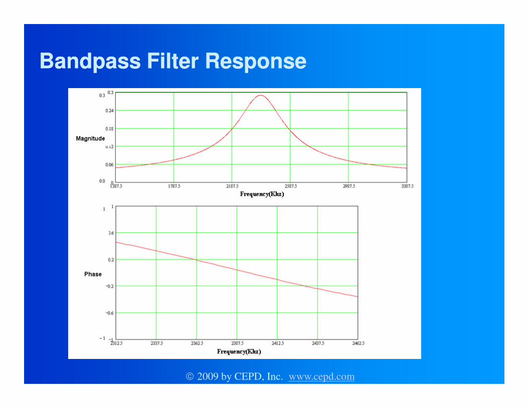
Bandpass Filter ResponseBandpass Filter Response
� 2009 by CEPD, Inc. www.cepd.com
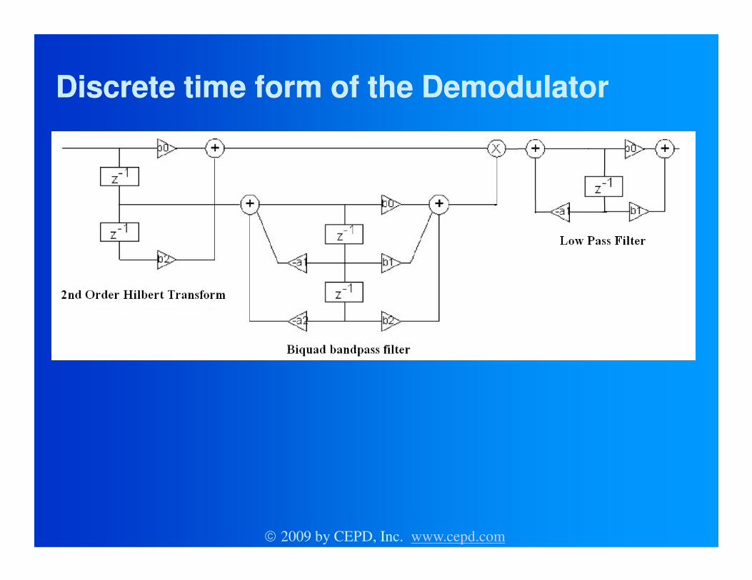
Discrete time form of the DemodulatorDiscrete time form of the Demodulator
� 2009 by CEPD, Inc. www.cepd.com

Lowpass Filter ResponseLowpass Filter Response
� 2009 by CEPD, Inc. www.cepd.com
Suggested ReadingSuggested Reading[1] Coffing, Danielle. Main, Eric. “Quadrature Demodulator,” TechOnline, Paper 14378, Jun. 4, 2001[2] Bilotti, Alberto. “Applications of a Monolithic Analog Multiplier,” IEEE Journal of Solid–State Circuits, Vol. SC–3, No. 4, December 1968. [3] Hentschel. Fettweis. “Sample Rate Conversion for Software Radio,” IEEE Communications Vol. 38, No. 8, pp. 142-150, August 2000.[4] Stark, Henry. Tuteur, Franz B. “Modern Electrical Communications: Theory and Systems” Prentice-Hall Inc. 1979.[5] Beach, Mark. MacLeod, John. Warr, Paul. Ed. Tuttlebee, Walter. “Software Defined Radio: Enabling Technologies.” John Wiley & Sons, Ltd. 2002.Enabling Technologies.” John Wiley & Sons, Ltd. 2002.[6] Rohde, Ulrich. Whitaker, Jerry. “Communications Receivers: DSP, Software Radios, and Design.” 3rd Edition. McGraw-Hill. 2001.[7] Vaughan, Rodney G. Scott, Neil L. White D. Rod. “The Theory of Bandpass Sampling.” IEEE Transactions on Signal Processing, Vol. 39, No. 9, pp.1973-1984, September 1991.[8] Farrell, David J. Williams, David M. “Implementation of Digital Filters in Programmable Logic Devices.” Class 551, Embedded Systems Conference, San Francisco, Spring 2001.[9] Farrell D., Oakley A., and Lyons R.; "Discrete-Time Quadrature FM Detection," IEEE Signal Processing Magazine, September 2005[10] “A Technical Tutorial on Digital Signal Synthesis,” Analog Devices 1999.[11] Lathi B.P.; “Modern Digital and Analog Communication Systems.” 3rd Edition. Oxford University Press. 1998.[12] Sayre Cotter W.; “Complete Wireless Design.” McGraw-Hill. 2001.
� 2009 by CEPD, Inc. www.cepd.com
Suggested Reading ContinuedSuggested Reading Continued[13] “United States RBDS Standard” National Association of Broadcasters. April 1998.[14] R. Lacoste, “Direct Digital Synthesis 101”, Circuit cellar 217, 2008
� 2009 by CEPD, Inc. www.cepd.com

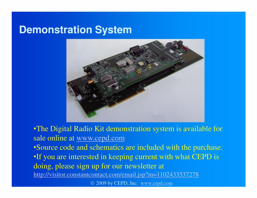
Demonstration SystemDemonstration System
A VHF FM Transceiver • Utilizes a conventional mixer front end with
an IF of 10.7MHz • A high speed ADC samples the IF at
66.5MHz.66.5MHz.• A modular FPGA board decimates the signal
and performs the modulation and demodulation.
� 2009 by CEPD, Inc. www.cepd.com
Demonstration SystemDemonstration System
•The Digital Radio Kit demonstration system is available for sale online at www.cepd.com•Source code and schematics are included with the purchase.•If you are interested in keeping current with what CEPD is doing, please sign up for our newsletter at http://visitor.constantcontact.com/email.jsp?m=1102433537278
� 2009 by CEPD, Inc. www.cepd.com

Beginning of Extra Supplemental Slides Beginning of Extra Supplemental Slides (the following were excluded from the talk)(the following were excluded from the talk)
� 2009 by CEPD, Inc. www.cepd.com

FM Modulation FM Modulation –– PrePre--emphasisemphasis
• Preemphasizing the transmitted signal can reduce noise greatly.– Noise increases linearly with frequency. – Weaker high frequency components (beyond 2.1kHz) are
boosted before the modulator using a preemphasis filter with a transfer function of Hp(j�). p
– The higher frequency components are deemphasized in the receiver using a deemphasis filter with a transfer function of 1/Hp(j�).
� 2009 by CEPD, Inc. www.cepd.com
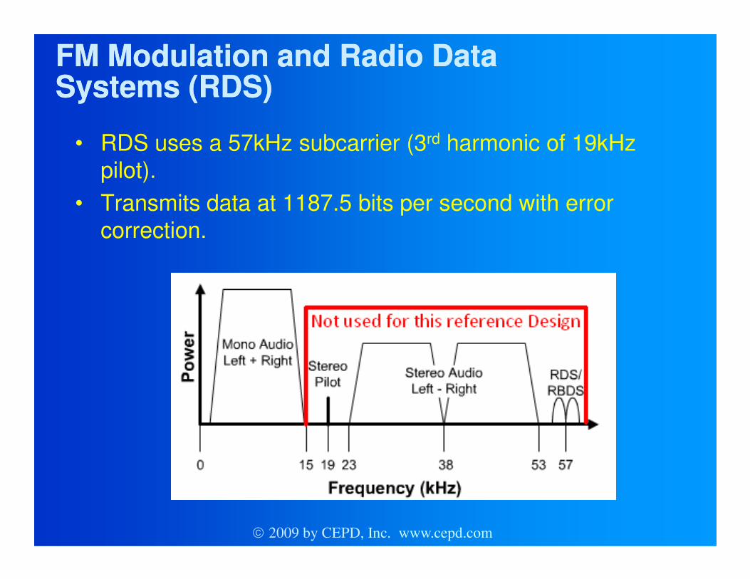
FM Modulation and Radio Data FM Modulation and Radio Data Systems (RDS)Systems (RDS)
• RDS uses a 57kHz subcarrier (3rd harmonic of 19kHz pilot).
• Transmits data at 1187.5 bits per second with error correction.
� 2009 by CEPD, Inc. www.cepd.com
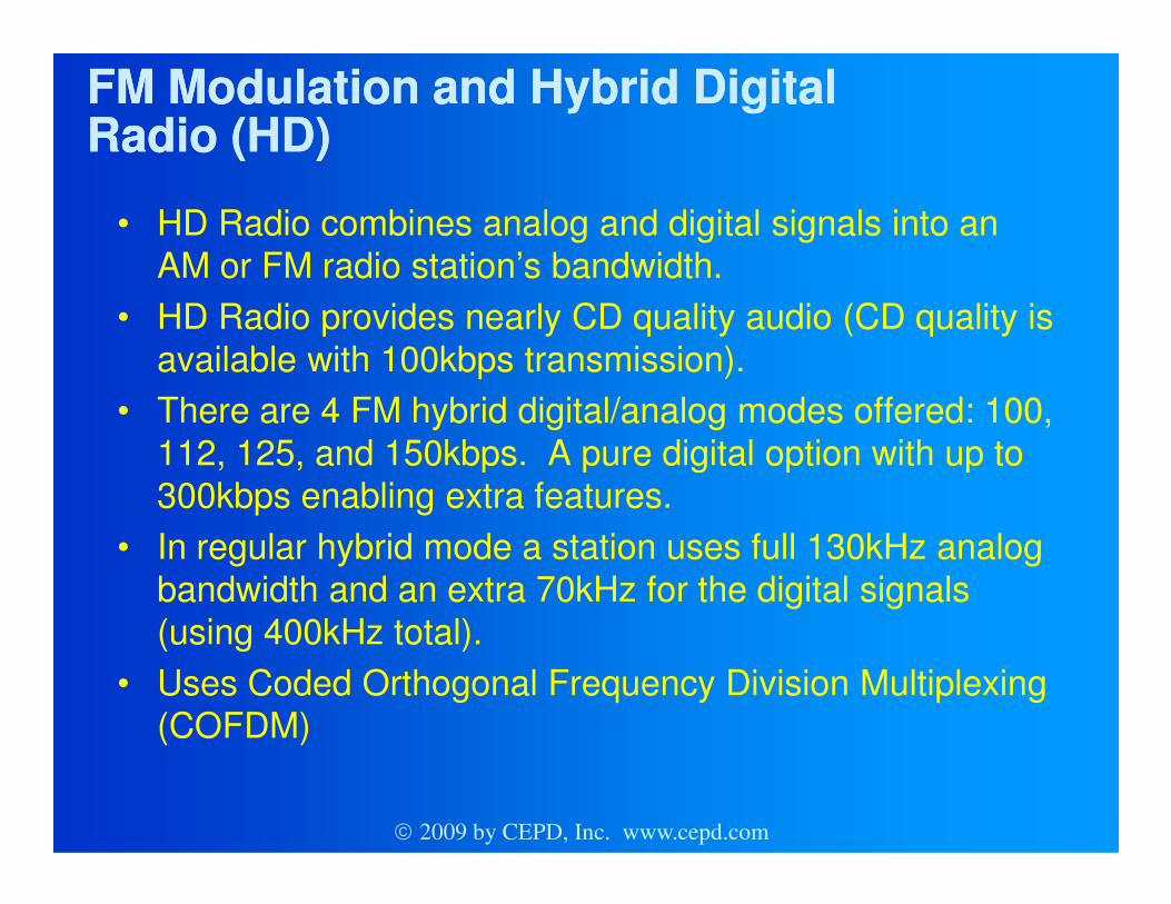
FM Modulation and Hybrid Digital FM Modulation and Hybrid Digital Radio (HD)Radio (HD)
• HD Radio combines analog and digital signals into an AM or FM radio station’s bandwidth.
• HD Radio provides nearly CD quality audio (CD quality is available with 100kbps transmission).
• There are 4 FM hybrid digital/analog modes offered: 100, 112, 125, and 150kbps. A pure digital option with up to 112, 125, and 150kbps. A pure digital option with up to 300kbps enabling extra features.
• In regular hybrid mode a station uses full 130kHz analog bandwidth and an extra 70kHz for the digital signals (using 400kHz total).
• Uses Coded Orthogonal Frequency Division Multiplexing (COFDM)
� 2009 by CEPD, Inc. www.cepd.com
Overview of DDS ArchitectureOverview of DDS Architecture
• A simple sine wave oscillator can be created using a reference clock, counter, and sine wave look up table. – This implementation is not flexible for generating
different frequencies as to generate other frequencies requires changes to the reference clock. requires changes to the reference clock.
• Modulation based on divide counters are difficult to implement as division is required to move between time and frequency.
� 2009 by CEPD, Inc. www.cepd.com

Performance of FM ModulatorPerformance of FM Modulator
10.7MHz29M
Hz
� 2009 by CEPD, Inc. www.cepd.com

What is meant by “portable VHDL”What is meant by “portable VHDL”• The code is not vendor specific • IP cores are not used• All of the source code is visible to the designer
-- Example: The Hilbert Transform w0_1 <= x; B0W0_1 <= b0_1 * w0_1; B2W2_1 <= b2_1 * w2_1; rightsum1 <= B0W0_1 + B2W2_1;
PROCESS (reset, demodClk) BEGINIF (reset = '1') THEN
w1_1 <= (others => '0'); -- clear tapsw2_1 <= (others => '0');y_1 <= (others => '0');
ELSIF (demodClk'EVENT and demodClk = '1') THEN w2_1 <= w1_1; -- update tapsw1_1 <= w0_1;y_1 <= rightsum1(31 DOWNTO 16); -- right shift for Q16
END IF;END PROCESS;
� 2009 by CEPD, Inc. www.cepd.com
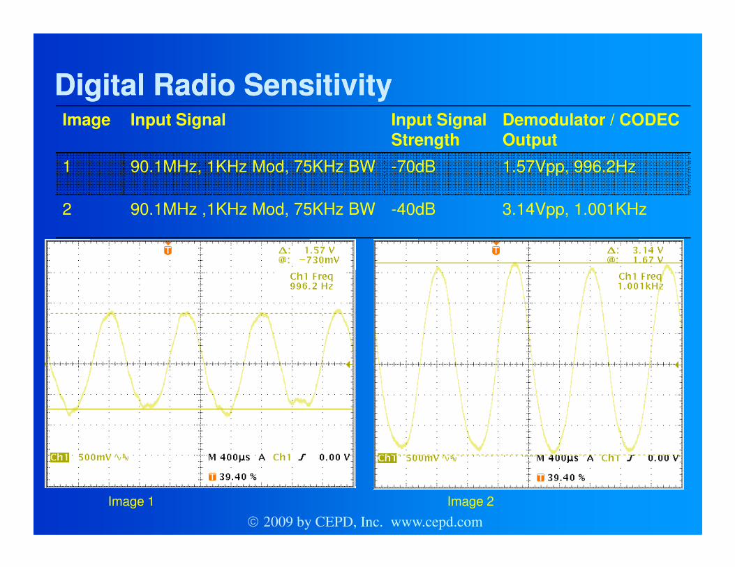
Digital Radio SensitivityDigital Radio SensitivityImage Input Signal Input Signal
StrengthDemodulator / CODEC Output
1 90.1MHz, 1KHz Mod, 75KHz BW -70dB 1.57Vpp, 996.2Hz
2 90.1MHz ,1KHz Mod, 75KHz BW -40dB 3.14Vpp, 1.001KHz
Image 1 Image 2
� 2009 by CEPD, Inc. www.cepd.com

FixedFixed--point Representationpoint Representation
1.3125 = 01 0101000000 Q1021 20 2-1 2-2 2-3 2-4 2-5 2-6 2-7 2-8 2-9 2-10
� 2009 by CEPD, Inc. www.cepd.com
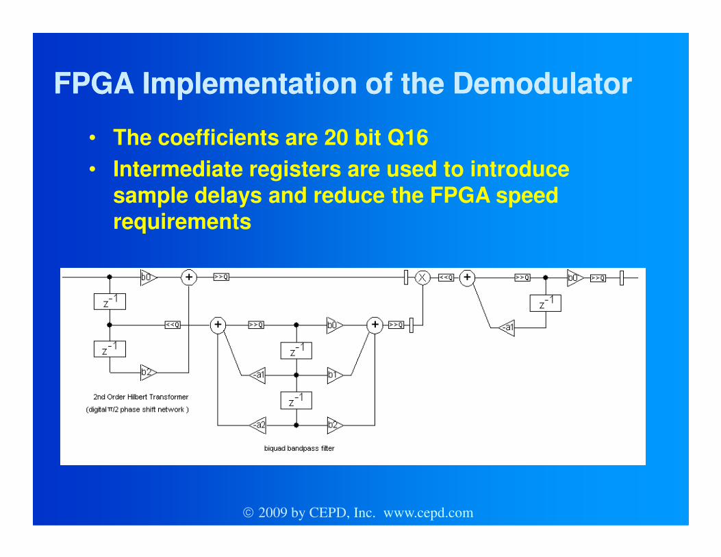
FPGA Implementation of the DemodulatorFPGA Implementation of the Demodulator
• The coefficients are 20 bit Q16• Intermediate registers are used to introduce
sample delays and reduce the FPGA speed requirements
� 2009 by CEPD, Inc. www.cepd.com