digital system design using vhdl - openstax...
TRANSCRIPT

Digital System Design using VHDL
By:Bijay_Kumar Sharma


Digital System Design using VHDL
By:Bijay_Kumar Sharma
Online:< http://cnx.org/content/col11213/1.8/ >
C O N N E X I O N S
Rice University, Houston, Texas

This selection and arrangement of content as a collection is copyrighted by Bijay_Kumar Sharma. It is licensed
under the Creative Commons Attribution 3.0 license (http://creativecommons.org/licenses/by/3.0/).
Collection structure revised: April 1, 2013
PDF generated: April 3, 2013
For copyright and attribution information for the modules contained in this collection, see p. 178.

Table of Contents
1 EC1561_Syllabus of Digital System Design using VHDL . . . . . . . . . . . . . . . . . . . . . . . . . . . . . . . . . . . . . 12 Digital System Design_Chapter 1_Part 1-Historical Background of IC
Technology. . . . . . . . . . . . . . . . . . . . . . . . . . . . . . . . . . . . . . . . . . . . . . . . . . . . . . . . . . . . . . . . . . . . . . . . . . . . . . . . . . . . . . 33 Digital System_Design_Chapter 1_Part 2_Introduction to VLSI . . . . . . . . . . . . . . . . . . . . . . . . . 174 DSD_Chapter 2_Basics of PLDs . . . . . . . . . . . . . . . . . . . . . . . . . . . . . . . . . . . . . . . . . . . . . . . . . . . . . . . . . . . . . . 275 Digital System Design_Chapter 2_Section 2_Wishlist of Digital System
Designer. . . . . . . . . . . . . . . . . . . . . . . . . . . . . . . . . . . . . . . . . . . . . . . . . . . . . . . . . . . . . . . . . . . . . . . . . . . . . . . . . . . . . . . 436 DSD_Chapter 3_VHDL._introduction and content . . . . . . . . . . . . . . . . . . . . . . . . . . . . . . . . . . . . . . . . . 537 DSD_Chapter 4_VHDL application to combinatorial logic synthesis . . . . . . . . . . . . . . . . . . . . . . 758 DSD_Chapter 4_VHDL application to sequential logic synthesis . . . . . . . . . . . . . . . . . . . . . . . . . . 919 DSD_Chapter 4_VHDL application to Sequential Circuit Synthe-
sis_Part2 . . . . . . . . . . . . . . . . . . . . . . . . . . . . . . . . . . . . . . . . . . . . . . . . . . . . . . . . . . . . . . . . . . . . . . . . . . . . . . . . . . . . . 10510 Chapter 5_ DSD_Moore and Mealy State Machines. . . . . . . . . . . . . . . . . . . . .. . . . . . . . . . . . . . . . . 12111 DSD_Chapter 5_StateMachines_Part3_MooreMachine Motor Rota-
tion Sensor Design and Synthesis. . . . . . . . . . . . . . . . . . . . . . . . . . . . . . . . . . . . . . . . . . . . . . . . . . . . . . . . . . 13912 DSD_Chapter 5_Part 3_Design of a Mealy Machine_Rotation_Sensor . . . . . . . . . . . . . . . . . 14913 DSD_Chapter 5_Supplement_Optical TERA BUS . . . . . . . . . . . . . . . . . . . . . . . . . . . . . . . . . . . . . . . 15714 DSD_Chapter 6_Mighty Spartans in Action_Introduction. . . . . . . . . . . . . . . . . . . . . . . . . . . . . . 16115 DSD_Chapter 6_Mighty Spartans in Action_Part 1_Digital Instru-
ments_Clocks+Scoreboard+the like . . . . . . . . . . . . . . . . . . . . . . . . . . . . . . . . . . . . . . . . . . . . . . . . . . . . . . . 167Index . . . . . . . . . . . . . . . . . . . . . . . . . . . . . . . . . . . . . . . . . . . . . . . . . . . . . . . . . . . . . . . . . . . . . . . . . . . . . . . . . . . . . . . . . . . . . . . 177Attributions . . . . . . . . . . . . . . . . . . . . . . . . . . . . . . . . . . . . . . . . . . . . . . . . . . . . . . . . . . . . . . . . . . . . . . . . . . . . . . . . . . . . . . . .178

iv
Available for free at Connexions <http://cnx.org/content/col11213/1.8>

Chapter 1
EC1561_Syllabus of Digital System
Design using VHDL1
1.1 EC1X66 [3-1-0]
1.2 Digital Systems Design using VHDL
Pre-requisite: EC1303[3_0_3]Digital ElectronicsHistorical Background of Integrated Circuit Technology- Evolution of IC Chips in terms of packing
density, clock speed; Computer Aided Design of IC Chips, Moore's Law. [4L]Introduction to Digital System Design- Simple Programmable Logic Devices(SPLD), Complex Pro-
grammable Logic Devices(CPLD), Field Programmable Gate Array(FPGA), Application Speci�c IntegratedCircuit(ASIC); [8L]
Basics of VHDL-VHDL: An Introduction , Why VHDL, Characteristics , Basic Structure , Data Ob-jects, Data Types, Combinational Logic Statements, Sequential Logic Statements, Concurrent Statements,Function, Procedure, Packages, Con�gurations. [10 L]
Implementation of Logic Design (both combinatorial and sequential) using VHDL. Validation of LogicDesign using Test Benches. [10L]
Moore and Mealy State Machine,Moore and Mealy variants, output of state machine, Moore Machine withclocked outputs, Mealy Machine with clocked outputs, state coding, residual states,optimum state machinein VHDL, asynchronous state machine [10L].Total 42 Lectures + 14 hours tutorial[Hand on practice onXilinx and ModelSim].
Text Book: VHDL for Engineers, Kenneth Short, Perason.Reference Books:
1. VHDL for Designers, Stefan Sjoholm & Lennart Lindh, Prentice Hall.2. Principles of Digital System Design using VHDL, Roth John, CENGAGE Learning,2010.
1This content is available online at <http://cnx.org/content/m34860/1.4/>.
Available for free at Connexions <http://cnx.org/content/col11213/1.8>
1

2 CHAPTER 1. EC1561_SYLLABUS OF DIGITAL SYSTEM DESIGN USINGVHDL
Available for free at Connexions <http://cnx.org/content/col11213/1.8>

Chapter 2
Digital System Design_Chapter 1_Part
1-Historical Background of IC
Technology.1
Digital System Design_Chapter 1_Part 1-Historical Background of IC Technology.Contents:
A. Chip design in brief.B. Chip design application areas.C. Latest chip design trend.D. Fabrication prospect.E. Conclusion.
Chip design in brief
1. Historical Journey2. VLSI Techniques3. New FPGA Revolution4. Embedded advantages
Historical Journey:
• Just after the invention of transistors in the end of 1947 and the beginning of 1948, SolidState Devices gradually started supplanting Vacuum Tubes . Vacuum Tubes becameobsolete because of large size, large electrical power consumption and higher cost. Thismarked the dawn of Solid State Era. Today by and large Vacuum Tubes have beentotally replaced by Solid State Devices except in RF and Microwave Wave very highpower generation and transmission where we are still using triode, pentode, klystron,magnetron and travelling wave tube.
• In 1959, Jack Kilby of Texas Instrument and Robert Noyce of Fairchild integrated acomplete RTL NAND gate on one silicon chip. This marked the birth of IntegratedCircuit Technology. This IC Technology was to have such a deep impact on Engineeringin particular and on Human Society in general that it ushered in the Third Wave ofCivilization(�rst wave of civilization was ushered in by agriculture and animal husbandry
1This content is available online at <http://cnx.org/content/m34693/1.4/>.
Available for free at Connexions <http://cnx.org/content/col11213/1.8>
3

4 CHAPTER 2. DIGITAL SYSTEM DESIGN_CHAPTER 1_PART1-HISTORICAL BACKGROUND OF IC TECHNOLOGY.
and second wave of civilization was ushered in by James Watt Steam Engine) and ThirdInformation Revolution (�rst information revolution was marked by the invention of al-phabets by Phoenicians and second information revolution was triggered by the inventionof Rotating Printing Press by Guttenburg, a German Technician).
Table 1. Growth of level of integration with the development and innovation in lithographictechniques and in the various processing steps in IC manufacture
IC No. of ActiveDe-vices Transis-tor/FET/BJT
Functions Year
SSI 1-100 Gates, OP-Amp, linearApp.
1960
MSI 100-1,000 Registers, Filters 1965
LSI 1,000-10,000 Microprocessor, ADC 1970
VLSI 10,000-100,000 Memory,Computers,SignalProcessors
1975
U LSI 100,000- 40,000,000 Pentium IV. 2001
40,000,000-50,000,000 Dual Core and QuadCore Procesors.
2010
Table 2.1
Available for free at Connexions <http://cnx.org/content/col11213/1.8>

5
Figure 2.1
Figure 1. Magni�ed view of the circuit layout on microprocessor chip 4004-the �rst µP chipintroduced in 1971.
IC Era (from SSI to VLSI)IC in 1960s:
• Only 2 transistors and one resistor.• Size of chip was more than required.• Unable to deal with complex functionalities.• Excess power dissipation.• Speed/Clock was in kHz.
IC in 2010s:
• Billions of transistors and other components.• Every part of chip is utilized.• E�cient in dealing with complex functionalities.• Power dissipation brought in control.• Million of operations can be done in just one second.
Table 2. Technology Characteristics of DRAM
Available for free at Connexions <http://cnx.org/content/col11213/1.8>

6 CHAPTER 2. DIGITAL SYSTEM DESIGN_CHAPTER 1_PART1-HISTORICAL BACKGROUND OF IC TECHNOLOGY.
Year of First DRAM Shipment 1995 1998 2001 2004 2007 2010
Minimum Feature Size (um) 0.35 0.25 0.18 0.13 0.10 0.07
Memory in bits/ chip 64M 256M 1G 4G 16G 64G
Microprocessor transistor/chip 12M 28M 64M 150M 350M 800M
ASIC(Gate/Chip) 5M 14M 26M 50M 210M 430M
Chip freq. MHz for high freq. on chip clock 300 450 600 800 1000 1100
Power Supply (V) 3.3 2.5 1.8 1.5 1.2 0.9
Maximum Power (mW) 80 100 120 140 160 180
Table 2.2
IC Computer-Aided-Design Technique from layout level to system leve l
Figure 2.2
Figure 2. Computer Aided Design of IC Chips of increased complexity.Initially up to 10,000 transistors, Microwind software tool was used at layout design level. As the density
of integration improved from10,000 transistors to 500,000 transistors DACK software was used at logic level.From 500,000 transistors to 50 million transistor VHDL is used. This is Register Level integration. VHDLis the acronym for Very_high _speed_integrated_circuit_Hardware _Description_Language. With thedevelopment of `DualCore' and `QuadCore' processors transistor count is exceeding 50 million and reaching50billion integration density. At this level of complexity System Level Description (SystemC) Language isused.
The introduction of HDLs and SystemC have made possible the design of complete system on chip (SOC),with the complexities rising from 1 million to 10 million transistors. Recently system C has been introducedfor 100 million to 1000 millions of transistors.
IC Design Growth at frequency level
Available for free at Connexions <http://cnx.org/content/col11213/1.8>
7
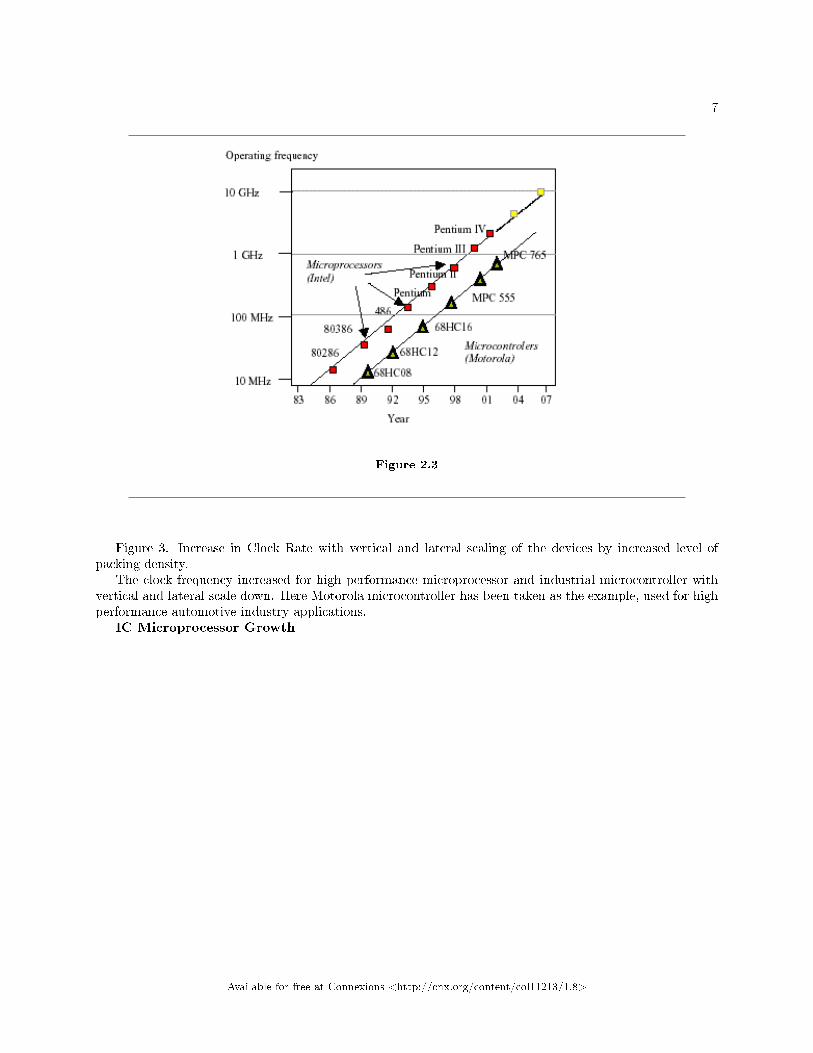
Figure 2.3
Figure 3. Increase in Clock Rate with vertical and lateral scaling of the devices by increased level ofpacking density.
The clock frequency increased for high performance microprocessor and industrial microcontroller withvertical and lateral scale down. Here Motorola microcontroller has been taken as the example, used for highperformance automotive industry applications.
IC Microprocessor Growth
Available for free at Connexions <http://cnx.org/content/col11213/1.8>

8 CHAPTER 2. DIGITAL SYSTEM DESIGN_CHAPTER 1_PART1-HISTORICAL BACKGROUND OF IC TECHNOLOGY.
Figure 2.4
Figure 4. Growth in packing density with the new generations of Microprocessors.Figure 4, describes the evolution of complexity of Intel @ microprocessor in terms of devices on the chip.
The Pentium4 processor, produced in 2003 is 40 million MOS devices integrated on a single piece of siliconno larger than 2 X 2 cm.
Evolution of Memory Size
Available for free at Connexions <http://cnx.org/content/col11213/1.8>

9
Figure 2.5
Figure 5. The growth in packing density of DRAM with improvement in Technology.First 1 kb memory was produced by Intel in 1971. Since then semiconductor memory have advanced both
in density as well as performances. 256 Mb memories was produced in 2000 and 1Gb in 2004. According tofuturistic estimates , it is expected to increase up to 16 Gb in 2008. This target has been achieved.
Evolution of Lithography
Available for free at Connexions <http://cnx.org/content/col11213/1.8>

10 CHAPTER 2. DIGITAL SYSTEM DESIGN_CHAPTER 1_PART1-HISTORICAL BACKGROUND OF IC TECHNOLOGY.
Figure 2.6
Figure 6.Improvment in minimum feature size resolution with advancement in Lithography Technique.Micron region of lithography is when the smallest feature size is from 10µm to 1µm.Submicron region is when smallest feature size is from 1µm to 0.1µm.Deep submicron region is when smallest feature size is 0.1µm to 0.01µm(or 100nm to 10nm)Ultra Deep submicron region is when smallest feature size is 0.01µm to 0.001µm (or 10nm to 1nm).Over the years Lithography has undergone through phases of development progressively resolving smaller
feature sizes . In 1962 we had contact printing, then we had proximity printing, next projection printing,followed by Electron-beam lithography, X-Ray lithography, G-line lithography, I-line Lithography. Thesmallest feature size had improved from 7µm to 0.80µm.
Next came Submicron Technology using Deep Ultra-Violet 248nm(DUV248nm) wavelength optical lithog-raphy. This could resolve 0.45µm feature size. This was followed by DUV193nm, followed byDUV157nm.We reverted back to DUV193nm in 1999 with a resolution of 0.18µm. In 2001 at same wavelength theresolution of 0.13µm was achieved. At 0.13µm resolution, 30Mgates could be implemented on 1cm by 1cmchip.
In 2003 Deep submicron Technology using DUV193nm but an improved source of ArF Excimer in placeof KrF Excimer a resolution of 0.09µm.
At 0.09µm or 90nm resolution, 100Mgates could be implemented in the same area. In 2005 using thesame light source but introducing immersion technique a further reduction in feature size is achieved namelyof 0.04µm. In future with the use of Extreme UV at wavelength of 100nm, the smallest feature size of 0.03µmor less will be achieved.
Ultra Deep submicron Technology will be born when we realize the smallest feature size less than 10nmwhich is long way o�.
As the lateral feature size has reduced so has the vertical junction depth as is evident from the following
Available for free at Connexions <http://cnx.org/content/col11213/1.8>

11
Table 3.Table 3. Dimension Scaling in MOSFET over the last decade.
MOS 1967 1997 1999 2001 2003 2006
L(µm) 10 0.25 0.18 0.13 0.1 0.07
DRAM(Gb/cm2) 64k 0.18 0.38 0.42 0.91 1.85
Junction Depth(xj)nm 1000 100 70 60 52 40
Interconnection pitch(nm) 2000 600 500 350 245 130
Table 2.3
Evolution of silicon area for NAND gateFigure shows, how fabrication for simple NAND gate become complex as its feature size is decreasing
almost exponentially.
Figure 2.7
Figure 7. Phases in lateral scaling with increase in packing density.When the smallest feature size is 1.2µm then a simple 2 Input NAND gate occupies 600µm2.When the smallest feature size is 0.35µm then a simple 2 Input NAND gate occupies 230µm2.When the smallest feature size is 0.12µm then a simple 2 Input NAND gate occupies 100µm2.When the smallest feature size is 0.09µm then a simple 2 Input NAND gate occupies 40µm2.
Available for free at Connexions <http://cnx.org/content/col11213/1.8>

12 CHAPTER 2. DIGITAL SYSTEM DESIGN_CHAPTER 1_PART1-HISTORICAL BACKGROUND OF IC TECHNOLOGY.
Thus linear lateral scaling leads to exponential increase in packing density and performance but at amuch higher cost because of the complexity of processing involved at smaller and smaller feature size.
Lithography mask cost doubles for every next generation and design team becomes larger.Table 4. Team size growth with the complexity of the circuit.
Year 1970 1990 2010
Typical size of design team 5000 for custom IC 50,000ForASIC 500,000ForFPGA
Table 2.4
Typical Structure of IC Dual-in-Line (DIP) package
Figure 2.8
Figure 8. Silicon Chip mounting on the ceramic header and ceramic dual-in-line package plugged in ICsocket which in turn is connected to the Printed Circuit Board.
Moore's Law :Doubling of transistors with IC Technology Growth at 18 months interval.Gordon Moore predicted that number of transistors on integrated circuits ( a rough measure of computer
processing power) will double every 18 months at a minimum cost. It became a self ful�lling prophecy.Moore's Law has become a yardstick of our progress as we harness the cunning of NATURE's design strate-gies.
Available for free at Connexions <http://cnx.org/content/col11213/1.8>

13
Figure 2.9
Figure 9. Validation of Moore's Law.In other words, the minimum feature size must decrease by a factor of 0.7 every three years.IC Process Plant
Available for free at Connexions <http://cnx.org/content/col11213/1.8>

14 CHAPTER 2. DIGITAL SYSTEM DESIGN_CHAPTER 1_PART1-HISTORICAL BACKGROUND OF IC TECHNOLOGY.
Figure 2.10
Figure 10. An ultra- clean room of IC manufacturing plant where all the workers arecovered in Nylon Aprons from top to bottom to keep out the dust they may be carrying.
Intel Pentium II Microprocessor
Available for free at Connexions <http://cnx.org/content/col11213/1.8>

15
Figure 2.11
Figure 11. Magni�ed photograph of top view of Intel Pentium II Chip.Core Computing in Computers.The processor speed has increased 10 times from Pentium in 1993 to Pentium III in 1999 but with theintroduction of Core2Duo in 2006 to Corei7 in 2013 the core speed has increased 1.5 times only but the needfor high speed computing is increasing exponentially. So obviously this paradigm of core computing will notbe able to keep up with the computing needs of the post-industrial era. So new computing paradigms willhave to be invented.
One of them is Memristor as a circuit element whose resistance drops as current �ows through it. HPand South Korean Firm Hynia are expected to launch next year the �rst memristor based Memory Chipsas a replacement of Flash Memory which has the least access time presently. Toshiba has announced theavailability of its 0.165m page-mode 64Mb and 128Mb NOR Flash memories that feature a random accesstime of 60ns and page access time of 20ns. Suitable for use in mobile phones, PDAs, and other wirelesshandheld applications that require high-performance memory, the devices operate from 2.3V to 3.6V, anddraws 55mA when reading, 15mA for program/erase functions, and 1mA during standby. The memristorwill provide the alternative to Flash Memory in the coming days.
The second possibility is that Graphene based Device may be marketed as the displays in Smart Phones.Graphene though a product of low-tech has high-tech performance. Flatland of Graphene is Alice's Won-derland.
Microelectronics engineers are paying attention to Graphene Technology. In semiconductor heterostruc-tures used to make FET devices, for instance, it takes million-dollar epitaxy machines and exquisite care totie up dangling surface bonds and eliminate impurities in quantum wells. The preparation minimizes thescattering of electrons against interfaces and defects to ensure the largest electron mean-free paths in thedevice. But this hi-tech processing requires a huge investment in infrastructure.
But in graphene devices comparable or even better results can be achieved at a much lower cost. 1 Åthick graphene: scientists have a material that is relatively defect free and whose electrons have a respectable
Available for free at Connexions <http://cnx.org/content/col11213/1.8>

16 CHAPTER 2. DIGITAL SYSTEM DESIGN_CHAPTER 1_PART1-HISTORICAL BACKGROUND OF IC TECHNOLOGY.
mean-free path naturally, without materials manipulation and processing. Graphene can hardly be more lowtech, and yet it still exhibits high conductivities. �It's really counterintuitive and remains to be understood,�comments Geim, �but the electron wavefunction appears to localize only parallel to the sheet and does notinteract with the outside world, even a few angstroms away.�
A third alternative is optical interconnects. These will speed up in-chip communication. One of thesethree technologies may take over the core functions of chip computing thereby provide an alternativeparadigm to core processing.Android Operating System based Gadgets drive the Consumer Electronics MarketExcerpted from �Android baked into Rice Cookers in move past Phones:Tech�. The Economic Times, Kolkota,9th February 2013, Wednesday.
Today Gadgets controlled via Internet have become the trend in Knowledge-based Society. During Agri-culture Phase we had Labour-intensive Society. During Industrial Phase we had Capital-intensive Society.In the present Industrial Phase we have Knowledge-intensive Society.
Google Inc's Android Operating System(OS) has become the most widely used Smart Phones OS. Theyhold 72% of the market in the third quarter(Q3) of the �nancial year 2012-13. While APPLE OS has 14%of the market according to Gartner Inc.
Annual Consumer Electronics Show in Las Vegas in 2013 is show casing Android based consumer andentertainment Gadgets such as:
1. Pico Pix Pocket Projector introduced by Royal Phillips Electronics NV. 2. Smart Thinq Refrigeratorsintroduced by LG Electronics Inc. 3. Asteroid Car Systems introduced by Parrot S.A. 4. Galaxy Camerasmarketed by Samsung.
Google by extending its OS free to new devices help Google collect data by which it can build morepowerful and lucarative Search Engines.
Android is an easy-to-use-platform that helps appliance makers like Samsung and Phillips to add newproduct features and bene�t from the demand for Internet-connected Devices and Gadgets
IDC (Interational Data Corporation) predicts that total turnover in such smart devices will reach $2Tril-lion turnover in 2015.
Since Android-based Phones went into sale in 2008, devices based on the mobile OS have surged inpopularity.
Building Android directly into Devices can help control these devices directly via Internet with minimalhuman intervention.For example TV may show a pop-up message from a clothes dryer in the basementindicating the status of the laundry.An Internet-connected rice cooking machine or cooker could set thecooking instructions itself once it is told the type of rice which has been loaded.
Making intelligent , internet-connected appliances have been the goal of manufacturers for years. Recente�orts to broaden the use of Android OS beyond phones and computers have yet to take a commercial shape.
Google tried to push into the living room via Google TV product.The set-top boxes and software for TV made by Sony and Logitech did not meet the sales goal after their
introduction in 2010.Hisense and Vizu plan to demonstrate models that use an updated version of Android for TV in Las
Vegas Annual Consumer Electronics Show.
Available for free at Connexions <http://cnx.org/content/col11213/1.8>

Chapter 3
Digital System_Design_Chapter
1_Part 2_Introduction to VLSI1
Digital System_Design_Chapter 1_Part 2Introduction to VLSIVERY LARGE SCALE INTEGRATION:�It is the process of integrating millions of transistors on tiny silicon chips to perform a multitude of logic
operation�How do we design such complex VLSI Chips?Programmable Logic Devices(PLDs) o�er a practical way of implementing large and complex Digital
Systems on IC chip.When a particular Digital System is required in very large quantity it may become more economical to
develop an optimized system dedicated to one particular application. IC chip implementation of such anoptimized, dedicated PLD is called Application Speci�c Integrated Circuits (ASIC).
For design & development of PLDs and ASIC we have sophisticated Electronic Design Automation(EDA) tools.
EDA design tools have reasonably kept pace with designers need as shown in the following chart:EDA design tools have gone fromTransistors↓Gate Level↓Register Transfer Level(RTL)↓Graphic Design System II(GDS II)Classi�cation of Programmable Logic Devices
1This content is available online at <http://cnx.org/content/m34695/1.3/>.
Available for free at Connexions <http://cnx.org/content/col11213/1.8>
17

18CHAPTER 3. DIGITAL SYSTEM_DESIGN_CHAPTER 1_PART
2_INTRODUCTION TO VLSI
Figure 3.1
Figure 12. Major Programmable Logic Devices.ROM and MPGA are programmed only once in the semiconductor fab itself whereas �eld programmable
can be programmed and reprogrammed according to the need. ROM is thought to be a Memory Device butit can used as combinational circuit also as already seen in Digital Electronics Theory Classes. MPGAs arepopular ways of achieving ASICs.
PLAs and PALs contain array of gates.PLAs contain programmable AND array and programmable OR array. This allows users to implement
combinational functions in two levels of gates.In PAL, OR array is �xed and AND array is programmable. PALs also contain �ip-�ops.Monolithic Memories Incorporation(MMI) and Advanced Micro Devices have developed a programming
language which converts Boolean equations into PLA con�gurations.Ultraviolet Erasures did not permit �eld programming. Only with the development of Electrically
Erasable Technology that �eld programmable PLDs became technically feasible.
SPLD CPLD FPGA
Density Few hundred gates 500 to 12000 gates 3000 to 5M gates
Timing predictable predictable unpredictable
Cost Low Medium High
Major Vendors Lattice Sem.;Cypress;AMD; Xilinx;Altera; Xil;Alt;Lat.Sem;Actel;
Device families L.S..GAL16LV8,GAL22V10; Xil..cool runner,XC9500; Xil..Virtex,Spartan;
Table 3.1: A comparison of Programmable Devices.
Table 5. A comparison of Programmable DevicesElectrically erasable CMOS PLD replaced PAL and PLA. PLDs contain macroblocks with array of gates,
multiplexers,Flip Flops or other standard Building Blocks.
Available for free at Connexions <http://cnx.org/content/col11213/1.8>

19
Lattice Semiconductor created similar devices with easy programmabilitty and called its line of devicesgeneric array logic or GAL.
PLAs, PALs, GALs, PLDs and PROM are collectively called Simple Programmable Logic Devices orSPLD.
When multiple PLDs are put together in the same chip with crossbar interconnection and have the sizesof 500 to 16000 gates then we achieve Complex Programmable Logic Devices.
In 1980 Xilinx created FPGAs using Static RAM. This integrates a large number of logic. FPGAs donothave gate array but they have bigger and complex blocks of Static RAM and multiplexers.
Seeing the performance of Xilinx, several PLD vendors and Gate Array Companies jumped into themarket. A variety of FPGA architecture were developed and used. Some are reprogrammable and some areone-time programmable fuse technologies. In last 15 years FPGAs have grown up to a size of 5 million gates.
Why VLSI ?
• Building complex electronic circuit using discrete components are di�cult and expensive - Cost dependson quantity of devices.
• Integrated circuits solved much of the problems
• Print many tiny circuits on a �at surface � �easy� as taking pictures.• Cost depends on die size.
• CPLD stands for Complex Programmable Logic Device, Advanced version of PLD's.
Here new resources are available such as Flip-Flops, Gates in high number and are able to give functionalityof circuits consisting of few thousand gates and few hundred �ip-�ops.
• FPGA (Field Programmable Gate Arrays) is another programmable resource having very higher pro-grammability than CPLD.
• Then there are other higher technology resources (ASIC's) which can be used to design many complexcircuit like microprocessors or bus controllers.
• Applications requiring user de�ned functions like bit processing or DSP algorithm combined with othercomputational capabilities.
• Thus you are actually designing for emerging and complex Technologies.
VLSI Advantages
1. Reduction in size, power, design, cycle time.2. Design security.3. Easy up-gradation.4. Low cost.5. Remote Programmability.6. Long time in market.
VLSI Techniques
• VLSI stands for Very Large Scale Integration. This is the technology of putting millions of transistorsinto one silicon chip.
• Tools (for VLSI):
A. Modelsim 6.2G: Simulation
Simulation is used for testing the behavior of outputs on the waveform according to their input given.
Available for free at Connexions <http://cnx.org/content/col11213/1.8>

20CHAPTER 3. DIGITAL SYSTEM_DESIGN_CHAPTER 1_PART
2_INTRODUCTION TO VLSI
A. Leonardo Spectrum 3: Synthesis
Synthesis tool is used for looking the hardware according to the program written in their language like,VHDL/ VERILOG.
A. Xilinx 10.1 ISE Pack: Chip downloading.
Evolution of programmable Devices:
1) PROM : Programmable ROM2) PAL : Programmable Array Logic.3) PLA : Programmable Logic Array.4) CPLD : Complex Programmable Logic Devices.5) FPGA : Field Programmable Gate Arrays.6) ASIC : Application Speci�c ICs.
PLD Trend
Figure 3.2
Figure 13.Volume of Application versus the building blockNew FPGA Revolution:
1) All disadvantages of ASICs have been overcome by FPGA namely:
a. Longer time to market.b. Complex Design Methodology.
2) In terms of No. of Transistors per chip, FPGA Venders have increased its capacity and astoundingresults are achieved as time pass through.
Available for free at Connexions <http://cnx.org/content/col11213/1.8>

21
3) Inclination towards FPGA is increasing day by day.4) Leverage existing design / chipset to support multiple display types.5) Faster time to market.6) Improve inventory control.7) Customize products for di�erent geographies.8) Reduce exposure to supply issues
a. Flexibility to e�ciently manage component supply problems.
9) Reacts quickly to competitive pressures
- Bringing new features / capabilities rapidly to market.FPGA Price Revolution:
Figure 3.3
Figure 14. Price of 100 K gates over time.Cost Management through System Integration:
Available for free at Connexions <http://cnx.org/content/col11213/1.8>

22CHAPTER 3. DIGITAL SYSTEM_DESIGN_CHAPTER 1_PART
2_INTRODUCTION TO VLSI
Figure 3.4
Figure 15. Cost management through System Integration.Embedded Advantage
• Complete System Design Possible.• Real Time Application.• Low Cost Chip.• VLSI goes on embedded as we can write program in Linux and Unix Environment.• System C developed by Xilinx.
Chip Design application Areas :
• VLSI in Wireless Communication• Digital Imaging• DSP Design• High Level synthesis• Logic Design• ASIC Design• Processor Design• Low Power Design• Issues in deep-sub micron VLSI• Electronic Design Automation (EDA) tools• Mixed Signal Design• All aspects of test and DFT• Most systems are now FPGA/ ASIC based• Networking (PCI, Ethernet USB)
Available for free at Connexions <http://cnx.org/content/col11213/1.8>

23
• DSP & Communication• Speech & Image Processing• Tele Mobile Communication• Microprocessor & Microcontroller based System• Home Appliances• Real Time Applications
Latest Chip Design Trend
• Auto Motive Sector• Biometric analysis for security• Neural Network & Arti�cial Intelligence• System on chip design with virtual component• Bio-chips: Rule Based System• Neuro Chips
FABRICATION PROSPECT:
1. Chip Design Productivity2. Chip Design Forecast3. World Fab Industry Vs Indian Fab Industry4. Why Fab lab does not exist in India?5. Challenges before Chip Design and Fab lab
Chip Design Productivity
Figure 3.5
Figure 16. Actual No. of Transistors in millions per IC design. This data illustrates thatthere is little correlation between transistors count and engineering e�ort.
Available for free at Connexions <http://cnx.org/content/col11213/1.8>

24CHAPTER 3. DIGITAL SYSTEM_DESIGN_CHAPTER 1_PART
2_INTRODUCTION TO VLSI
Figure 3.6
Figure 17. Normalized Transistors count Vs. Persons week.
Figure 3.7
Available for free at Connexions <http://cnx.org/content/col11213/1.8>

25
Figure 18: Factors In�uencing IC Design E�ortDesign Productivity = output produced /labour expended= output per unit worker hourManufacturing productivity = value added/labour expended= value added per unit worker hour.= (end product selling price- material cost of theproduct) worker hour= dollars per worker hourChip design productivity 6= transistor /gate per unit engineering e�ort.Chip design productivity = chip design complexity/ engineering e�ort.= complexity per unit engineering hour.= normalized transistors per person-hour.Chip Design Forecast :According to Indian Semiconductor Association (ISA) quoting the ISA-IDC Report of 2008, by that
year the Semi Conductor activity in India had a turn over of $ 7.37 billion employing over 150,000 highlyquali�ed professionals. Embedded Software Design constituted a whopping 81% of this activity with VLSIdesign being 13% and hardware / board design being 6%. The growth rate of this sector is some 20%annually, so we can expect a turnover in excess of $ 12 billion by the end of Year 2010 (employing 180,000+professionals) of which embedded system design would have a turnover of 10 billion. It is believed that theglobal embedded design activity is worth some $25 billion annually. This roughly amounts to India producinga quarter of the world's embedded design systems. The growth in the design business to the rapid growthof the Indian Electronics Industry from $363 billion by 2015 at a compounded annual growth rate of some30%, accounting for 11% of the global market by 2015, projected to grow to $ 155 billion by 2015.
World Fab Industry Vs Indian Fab Industry:
a. Around 50 Fab lab exist in the world, another 50 in near future.b. First Fab lab by Intel just open in Tiwan, �rst in South Asia.c. No complete VLSI Fab lab in India.d. SCL, Chandigarh has its own LSI fab lab.e. Proposal: Rs.1500 crore (for Indian Govt.).f. Recently, three companies joined forced in Fab industry like: Sem India, HEMC, and Allience Materials.
Fab lab does not exist in India: Why ?1. Huge fabrication Lab Cost:As fabrication unit requires minimum 1500 crore rupees investment, it's not feasible for many small
Indian companies to make sustained investments for a long period of time, which is required for productdevelopment (including the area of chips design/ manufacturing).
2. Design In competency, Probably India is not prepared:The actual problem is that quality talent with the right skills is becoming scarce. The skills required are
in vertical domains (DSP, TELECOM, etc.) along with in depth understanding of chip design challenges likedesigning for high speed, low power, small size, handling large complexities, accounting for deep sub-microne�ects like signal integrity.
Challenges before Chip Design and Fab Industry
1. System Level Integration: there is requirement of system engineers who can understand the com-plete system. The trend towards coding is to write code in C/C++, Matlab/ Java and converted intoHDL/ VERILOG, is not suitable.
2. Chip Design Limits: Chip Design, reported by New York Times by at Paul Packan, a scientist withIntel Corp., the world largest chipmaker, said semiconductor engineers have not found ways aroundbasic physical limits beyond the generation of silicon chips that will begin to appear next year. Packancalled the apparent impasse �the most di�cult changes the semiconductor industry has ever faced.�
Available for free at Connexions <http://cnx.org/content/col11213/1.8>

26CHAPTER 3. DIGITAL SYSTEM_DESIGN_CHAPTER 1_PART
2_INTRODUCTION TO VLSI
These fundamental issues have not previously limited the scaling of transistors,� Packan wrote in the Sept.24 issue of Science. �There are currently no known solutions to these problems.�
According to Dennis Allison, a Silicon Valley physicist and computer designer, if the miniaturizationprocess for silicon based transistors is halted, hopes for continued progress would have to be based on newmaterials, new transistor designs and advances like molecular
computing , the Times reported. This mystery will be solved ultimately.Can we meet the challenges of the Future?[�Can you meet the design challenges of 90nm and below?�, Electronic Design, 2005][�Nano-computers�, by Phillips J. Kurkes, Gregory S. Snider & R.Stanley William, Scienti�c American,
November 2005, 72-80.]Unprecedented manufacturing success has been achieved by enhancing the ability of number crunching,
executing enhanced FLOPS(�oating point operations per second)/Instructions per second and by enhanceddata storage capability.
Historically we have moved from labour intensive techniques to capital intensive techniques. Presentlywe are witnessing a movement towards knowledge intensive techniques.
Agricultural labour were replaced by proletariate(industrial labour) and proletariate are being replacedby cognetariate(knowledge worker).
Introduction of computerization, automation and robotization has changed the bench marks of life.Silicon Industry has become the largest and most in�uential industry.Silicon Industry has become the locomotive of economic development.Major innovation will be required to reach 10nm feature size. Finding alternative technologies that can
further shrink computing devices is crucial to maintaining technological progress. Alternative technologycould be `Quantum Computing' and `Cross-Bar Architecture'.
In Cross-Bar Architecture, one set of nano-wires cross another set of nano-wires at right angles. A specialmaterial is sandwiched at the intersection between the crossing wires. This sandwiched material could switchon and o�. Logic functions as well as memory functrions could be achieved using the intersections.
As the packing density increases, atomic defects become a serious problem. This problem could becircumvented by building redundancy and by using coding technique. By using Error Correcting Codes theerror rates at the intersection could be drastically reduced. By introducing 40% redundancy the yield ofmanufacturing could improve from 0.0001 to 0.9999 if the defect rate is 0.01.
Today Cross Bar Architecture has emerged as the principal contender for a new computing paradigm.For this success, architecture, device physics and nano-manufacturing techniques need to simultaneouslydevelop.
Cross Bare Architecture is ideal for implementing strategies based on �nding and avoiding defect areasand using coding theory to compensate for mistakes.
Such switches should be able to scale down to single atom dimension.
Available for free at Connexions <http://cnx.org/content/col11213/1.8>

Chapter 4
DSD_Chapter 2_Basics of PLDs1
Digital System Design_Chapter 2_Basic Philosophy of Simple Programmable Logic Devices(SPLD).In Chapter 1_ Part 2 we saw that PLAs, PALs, GALs, PLDs and PROM are collectively called Simple
Programmable Logic Devices. Here we will examine PLA, PAL and PROM closely to understand how exactlySum of Products Boolean Function is achieved.
CODE CONVERTERS- DECODER & ENCODER.All these programmable devices are based on the philosophy of M-bit Code Input being converted to
N-bit Code output.2M = µ and 2N = α.Here α may be less than µ. In that case each of the M-bit code does not have a corresponding unique
N-bit code. Many of the M-bit codes may have the same N-bit code.How does the code converter work:The �gure 1 gives the code converter working.
1This content is available online at <http://cnx.org/content/m34939/1.3/>.
Available for free at Connexions <http://cnx.org/content/col11213/1.8>
27

28 CHAPTER 4. DSD_CHAPTER 2_BASICS OF PLDS
Figure 4.1
Figure 1. Code-converter System.ROM is typical Code Converter system.Here M-bit decoder is AND system and N-bit encoder is OR system.Therefore:Each bit-line Yi = SUM of PRODUCT of X0,X1,X2. . ...X(m-1).Decoder Word Line generates PRODUCT terms.A DECODER is realized by Multiplexer also known as MUX. MUX is nothing but a combination of
AND gates. In Figure 2 we show a 4-bit binary to decimal decoder:
Available for free at Connexions <http://cnx.org/content/col11213/1.8>

29
Figure 4.2
Figure 2. 4-bit binary to decimal decoder.
Available for free at Connexions <http://cnx.org/content/col11213/1.8>

30 CHAPTER 4. DSD_CHAPTER 2_BASICS OF PLDS
Figure 4.3
Figure 3. Block Model of 4-bit binary to decimal decoder.Table 1. Truth Table of the decoder
D C B A Word Line Decoded Decimal Value
0 0 0 0 W0 0
0 0 0 1 W1 1
0 0 1 0 W2 2
0 0 1 1 W3 3
0 1 0 0 W4 4
0 1 0 1 W5 5
0 1 1 0 W6 6
0 1 1 1 W7 7
1 0 0 0 W8 8
1 0 0 1 W9 9
Table 4.1
In Figure 3, for every BCD code one of the 10 Word lines will go HIGH and the remaining lines will beLOW. Figure 2 tells us that every Word Line is a PRODUCT of 4 Variables A,B,C,D and their complementsA′ , B′,C′,D′ .
Encoder Bit Line is SUM of Words.Keyboard of a Computer generates 8-bit ASCII Code on pressing one of the keys. Hence Keyboard is
ENCODER ARRAY. For simplicity of presentation we present 10Key - 4bit Encoder. The customer willhave to decide and specify the 4-bit codes corresponding to 10 keys. That is the Customer will provide theTruth Table.
Available for free at Connexions <http://cnx.org/content/col11213/1.8>

31
Suppose the customer provides the following Truth Table 2:Table 2. The Truth Table of the Encoder.
W9 W8 W7 W6 W5 W4 W3 W2 W1 W0 Y3 Y2 Y1 Y0
0 0 0 0 0 0 0 0 0 1 0 0 0 0
0 0 0 0 0 0 0 0 1 0 0 0 0 1
0 0 0 0 0 0 0 1 0 0 0 0 1 0
0 0 0 0 0 0 1 0 0 0 0 0 1 1
0 0 0 0 0 1 0 0 0 0 0 1 0 0
0 0 0 0 1 0 0 0 0 0 0 1 0 1
0 0 0 1 0 0 0 0 0 0 0 1 1 0
0 0 1 0 0 0 0 0 0 0 0 1 1 1
0 1 0 0 0 0 0 0 0 0 1 0 0 0
1 0 0 0 0 0 0 0 0 0 1 0 0 1
Table 4.2
Available for free at Connexions <http://cnx.org/content/col11213/1.8>
32 CHAPTER 4. DSD_CHAPTER 2_BASICS OF PLDS
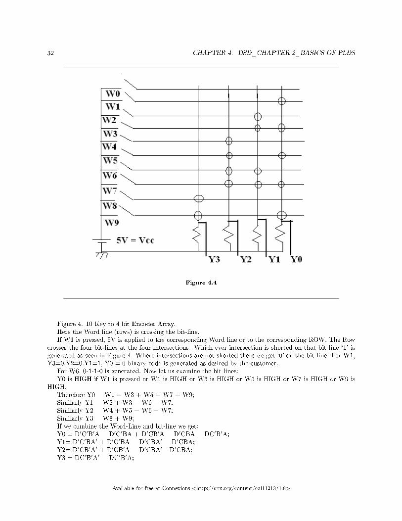
Figure 4.4
Figure 4. 10 Key to 4-bit Encoder Array.Here the Word line (rows) is crossing the bit-line.If W1 is pressed, 5V is applied to the corresponding Word line or to the corresponding ROW. The Row
crosses the four bit-lines at the four intersections. Which ever intersection is shorted on that bit line `1' isgenerated as seen in Figure 4. Where intersections are not shorted there we get `0' on the bit line. For W1,Y3=0,Y2=0,Y1=1, Y0 = 0 binary code is generated as desired by the customer.
For W6, 0-1-1-0 is generated. Now let us examine the bit lines:Y0 is HIGH if W1 is pressed or W1 is HIGH or W3 is HIGH or W5 is HIGH or W7 is HIGH or W9 is
HIGH.Therefore Y0 = W1 + W3 + W5 + W7 + W9;Similarly Y1 = W2 + W3 + W6 + W7;Similarly Y2 = W4 + W5 + W6 + W7;Similarly Y3 = W8 + W9;If we combine the Word-Line and bit-line we get:Y0 = D′C′B′A + D′C′BA + D′CB′A + D′CBA + DC′B′A;Y1= D′C′BA′ + D′C′BA + D′CBA′ + D′CBA;Y2= D′CB′A′ + D′CB′A + D′CBA′ +D′CBA;Y3 = DC′B′A′ + DC′B′A;
Available for free at Connexions <http://cnx.org/content/col11213/1.8>

33
Thus we have achieved 4 Sum-of-Product(SOP) Boolean Functions. By combining Decoder-Encoder weachieve AND-OR function which is the same as NAND-NAND function.
Figure 4.5
Figure 5. The combination of Decoder-Encoder is AND-OR gate.The above circuit is Programmable Logic Array.The AND terms are generated by shorting the A,B,C,D and A′, B′, C′, D′ lines or Columns with the
Rows of Input of Ten AND gates.The OR terms are generated by shorting the intersection of Word-line(rows) and bit-lines(columns)The shorting of intersection can be done putting a DIODE from the Word-line to bit-line as shown in
Figure 6.The shorting of intersection can be done by using multi-emitter BJT as shown in Figure 7.The shorting of intersection can be done using NMOS as shown in Figure 8.
Available for free at Connexions <http://cnx.org/content/col11213/1.8>

34 CHAPTER 4. DSD_CHAPTER 2_BASICS OF PLDS
Figure 4.6
Figure 6. Diode Matrix is used to generate OR terms.Diodes are the memory elements. Diode transfers `1' of Word-line to the corresponding Bit-line. The
output WORD for any input code may be read as many times as possible. But the stored relationshipbetween Input Code and Output Word cannot be modi�ed. The Diode Matrix is fabricated at the factorylevel. Hence this is Read-Only-Memory (ROM).
Available for free at Connexions <http://cnx.org/content/col11213/1.8>

35
Figure 4.7
Figure 7. Multiemitter BJTs are used for transferring `1' from Word-line to Bit-line with which theintersection is shorted.
Multiemitter BJT has four emitters. When an Emitter is shorted to Bit-line, BJT behaves like EmitterFollower and as soon as the WORD-line goes HIGH the shorted bit-line ( shorted with the given highWord-line) goes HIGH and all other bit-lines remain LOW.
According to customer requirement, the manufacturer shorts or opens the intersection by the use ofproper MASK. This is Custom Programming or Mask Programming or Hardware Programming. This is`One-Time Factory Programming'.
WORKING OF 4k-bit Static ROM.Static ROMs can be built of BJT or NMOS. These have no clock input. These are non-volatile. They
never lose data. They are available in 1 to 64kb range. NMOS StaticROM have access time 0.1 to 1 µsec.This access time is one order of magnitude longer than that of BJT StaticROM.
In a NMOS or BJT StaticROM we have a DECODER as shown in Figure 8. It has address input orselect input. In this case address word is 10-bit wide. Hence it can access 1024 locations of memory. Atevery location a 4-bit wide binary word can be stored as shown in Figure 9. When an address word arrives, one of the 1024 Word-lines goes HIGH. At any instant only one Word-line can go high.
Available for free at Connexions <http://cnx.org/content/col11213/1.8>

36 CHAPTER 4. DSD_CHAPTER 2_BASICS OF PLDS
Figure 4.8
Figure 8. Decoder for 4k-bit ROM.
Available for free at Connexions <http://cnx.org/content/col11213/1.8>

37
Figure 4.9
Figure 9.An NMOS ROM encoder ( Only 5 of the 1024 Word-lines are shown). Small circle means theintersection is shorted.
In Figure 8, when the following address word is applied:
B9 B8 B7 B6 B5 B4 B3 B2 B1 B0
0 0 0 0 0 0 0 0 0 0
Table 4.3
Then W0 line goes HIGH. This selects the DATA WORD `0110' in Figure 9.Let us examine Figure 9 closely:Q3 and the NMOSs in that ROW are Load FETs. Here Drain and Gate of NMOS have been shorted.
Hence Q3 and its corresponding elements act as loads of the bit-lines Y0,Y1,Y2,Y3.NMOS has the advantage that it can act in following manners:
i. as a Capacitor when you operate between Gate and Source;ii. as three terminal active element;iii. as a non-linear two terminal resistance when Gate and Drain are shorted together.
Available for free at Connexions <http://cnx.org/content/col11213/1.8>

38 CHAPTER 4. DSD_CHAPTER 2_BASICS OF PLDS
NMOSs in the Word-lines act as MEMORY ELEMENTS.All Bit-lines are at HIGH level. Because Vdd = 5V is being applied to all Bit-lines and all bit-lines at
the other end is simply hanging.When W0 goes HIGH, the intersections of Y1, Y2 and W0-line have no NMOS. Y1 = `1' and Y2 = `1'
state continues as it was before.At the intersection of Y0 and Y3 we have Q2 and Q4 NMOSs. Their Gates are connected to W0-line
which is presently held HIGH at 5V > Threshold Voltage of NMOS. Hence Q2 and Q4 turn ON and providea short to Ground. Therefore Y0 = `0' and Y3= `0'.
Here we are following ACTIVE-LOW Logic. Ordinarily bit-lines are at `1' and when ACTIVE they goLOW or go to `0'.
Thus with 0000000000 address word applied to the address bus of the given ROM, W0 gets selected and`0110' ,which is stored in the ROM memory space, gets READ out.
The following Table 1 gives the binary bits stored in locations selected by W0,W1,W2 and W500 word-lines.
Table 1. The Word address and the bit-outputs.
B9 B8 B7 B6 B5 B4 B3 B2 B1 B0 WORD-line Y0′ Y1′ Y2′ Y3′
0 0 0 0 0 0 0 0 0 0 W0 0 1 1 0
0 0 0 0 0 0 0 0 0 1 W1 1 0 0 1
0 0 0 0 0 0 0 0 1 0 W2 0 1 0 1
0 1 1 1 1 1 0 1 0 0 W500 1 1 0 0
Table 4.4
Here the Bits stored are pre-programmed and cannot be changed unless we �nd some methods to constructNMOS and omit NMOS at the 1024×4 ROM Memory Cells.
What we have shown is a Factory programmed ROM. Field programmed ROM had to wait for severalyears before it was introduced as Field Programmable Devices.
In the above example Y0 bar or Y0′ = W0 +W2;Y1′ = W1; Y2′ = W1 + W2 + W500; Y3' = W0 + W500;By inverting the bit-lines we obtain SOP Logic Functions.ROMs do not minimize the gates for a given CODE-conversion.Suppose the customer wants me to design `BCD to 7-Segment decoder-driver'.What this means that :Table 2. Decoding of BCD to Decimal NUMERIC value.
Available for free at Connexions <http://cnx.org/content/col11213/1.8>

39
BCD code Decimal Number to be displayed on 7-Segment display
0000 0
0001 1
0010 2
0011 3
0100 4
0101 5
0110 6
0111 7
1000 8
1001 9
Table 4.5
In Figure 10 we have shown the construction and the composite structure of 7-SEGMENT DISPLAY.In Figure 10 it is also shown as to which LED should glow corresponding to a decimal value. From thisknowledge we can construct the following Table 3 for code conversion.
Available for free at Connexions <http://cnx.org/content/col11213/1.8>

40 CHAPTER 4. DSD_CHAPTER 2_BASICS OF PLDS
Figure 4.10
Figure 10. Construction of Common Anode 7-Segment Display.Table 3. Conversion from a BCD to a Seven-Segment-Display Code.
BCD code Word-line Y6 Y5 Y4 Y3 Y2 Y1 Y0
DCBA g′ f′ e′ d′ c′ b′ a′
0000 W0= D′C′B′A′ 1 0 0 0 0 0 0
0001 W1= D′C′B′A 1 1 1 1 0 0 1
0010 W2= D′C′BA′ 0 1 0 0 1 0 0
0011 W3= D′C′BA 0 1 1 0 0 0 0
0100 W4= D′CB′A′ 0 0 1 1 0 0 1
0101 W5=D′CB′A 0 0 1 0 0 1 0
0110 W6= D′CBA′ 0 0 0 0 0 1 1
0111 W7= D′CBA 1 1 1 1 0 0 0
1000 W8= DC′B′A′ 0 0 0 0 0 0 0
1001 W9= DC′B′A 0 0 1 1 0 0 0
Available for free at Connexions <http://cnx.org/content/col11213/1.8>

41
Table 4.6
Since input code is 4 bits therefore there are 24 = 16 word lines hence Table 3 must have 6 extra Word-lines i.e. W10, W11, W12, W13, W14, W15. Corresponding to these 6 Word-lines there are some arbitrarySYMBOL displays depending upon the convenience of the Designer.
If all 16 Word-lines are considered then the bit-line Y0 will be by inspection of the Table:Y0= W1 + W4 + W6 + W10 + W11 + W14 + W15;By replacing the Word-line by their corresponding Product Term we get:Y0 = D′C′B′A + D′CB′A′ + D′CBA′ + DC′BA′ + DC′BA + DCB′A′ + DCBA′ + DCBA.By minimization technique we obtain:Y0 = D′C′B′A + CA′ + DB;Similarly minimized expressions can be obtained for all the remaining 6 bit-lines.If using the minimized expressions for Y0, Y1, Y2, Y3 Y4, Y5, Y6 we build the decoder-driver then
almost 20% saving in component count takes place as compared to a decoder-driver built by ROM. It can beeven more. But this will require extra man-hours for minimizing and designing. If the demand can justifythis extra cost then one could go for these especially designed and optimized circuits. These circuits arecalled `Application Speci�c Integrated Circuits'(ASIC). The `BCD to 7 Segment decoder-driver' presentlyavailable in the market by the component code 74HC4511 is one such ASIC circuits.
Available for free at Connexions <http://cnx.org/content/col11213/1.8>

42 CHAPTER 4. DSD_CHAPTER 2_BASICS OF PLDS
Available for free at Connexions <http://cnx.org/content/col11213/1.8>

Chapter 5
Digital System Design_Chapter
2_Section 2_Wishlist of Digital System
Designer.1
Digital System Design_Chapter 2_Section 2_Wishlist of Digital System Designer.The wishlist of Digital System Designer is to create a PLD where he downloads a programme and gets
the PLD con�gured for a certain number of functions. With passage of time a few more functions are to beadded and some existing functions are to be omitted. He would like to modify his programme and reload iton the same PLD. Economy-wise this would make sense. But this requires that he has Electrically Erasableand Reprogrammable PLD. This requires that it should be �eld-programmable.
In 1956, at the request of US Air-Force, Scientists of ARMA Division of American Bosch Arma Corpora-tion, Garden City, New York, developed a User Programmable ROM akin to Diode Matrix shown in Figure6 of Chapter 2_Section 1. The fresh ROM had a diode connected at all intersections. It implied state HIGHor `1' in all memory cells. The user could retain or omit the DIODE at the intersection as his design needbe. By applying a High Voltage Pulse of 30V which is not used in Digital Systems, the user could burn thewhiskers of the Diode and thereby �burn� / �Zap� / �blow� open the given diode. This would give `0' statein that particular Memory Cell which lies at the given intersection. This way by burning the requisite set ofmemory elements namely the diodes at the intersections, the desired functional relationship can be achieved.Once the requisite diodes are blown out, the functional relationship is unalterable. Hence this was calledOne-Time User Programmed ROM.
In1971, Intel Scientists at Santa Clara, California, developed Erasable Programmable ROM (EPROM).This new device was based on a special double-gate NMOS referred to as Floating-Gate Avalanche-InjectionMOS(FAMOS). This double-gate NMOS is shown in Figure 11.
1This content is available online at <http://cnx.org/content/m34940/1.2/>.
Available for free at Connexions <http://cnx.org/content/col11213/1.8>
43

44CHAPTER 5. DIGITAL SYSTEM DESIGN_CHAPTER 2_SECTION
2_WISHLIST OF DIGITAL SYSTEM DESIGNER.
Figure 5.1
Figure 11.Floating Double Poly-silicon gate structure NMOS used in EPROMIn Figure 9 of Chapter 2_Sec 1, we place such Double-Gate NMOS at all intersections as shown in Figure
12.
Available for free at Connexions <http://cnx.org/content/col11213/1.8>

45
Figure 5.2
Figure 12. EPROM using Double-Gate NMOS.Before user programming, FAMOS (Double-Gate NMOS) is present at all intersections. Any Word-line
going HIGH will place 0s at all the four Bit-lines. Hence e�ectively EPROM comes with 0s stored in allmemory cells. When the user applies 25V pulse between Gate2 and Drain, a high electric �eld is createdin the depletion region of the p-n junction of the Drain-substrate. This electric �eld is in excess of thecritical �eld. This results in Avalanche Breakdown. This creates a large reverse current. The electroncomponent of this breakdown current is accelerated towards Gate2. It penetrates the thin oxide regionand gets accumulated on Gate1. Gate 1 e�ectively becomes negatively charged hence 5V at Gate2 is nomore able to turn this transistor ON. Hence e�ectively the NMOS at that intersection is disabled and state`1' is permanently stored in that cell. Thus by application of 25V at the requisite intersections' FAMOS,the transistor is disabled and state `1' is permanently stored giving rise to the desired Boolean Function.Because of SiO2, charges accumulated on Gate2, do not discharge for 10years and longer. The `1s' storedby application of 25V at Gate2s can be easily erased by exposing the ROM to Ultra-Violet light. UV lightmakes the SiO2 slightly conducting thereby providing a path for leakage of charge accumulated on Gate1.Thus all disabled NMOSs are enabled and this restores EPROM to all `0s' states . This can once again bereprogrammed and recon�gured. But this requires long exposure time in excess of 2 minutes for completeeraser. Hence Electrically erasable and programmable ROM(EEPROM) became the need of the hour.
In 1978, once again the Scientists of INTEL developed and commercialized EEPROM. They reduced the
Available for free at Connexions <http://cnx.org/content/col11213/1.8>
46CHAPTER 5. DIGITAL SYSTEM DESIGN_CHAPTER 2_SECTION
2_WISHLIST OF DIGITAL SYSTEM DESIGNER.
thickness between Gate1 and Channel from 1000A ◦ (100nm) to 100A ◦ (10nm). Now 10V electric voltagepulse was su�cient to writ `1s' in a given cell. The same voltage reversed could erase `1' and reset the wholeROM to `0s'.
Thus we see the Digital Designer's wish list was ful�lled. Now he had a ROM which could be repro-grammed and recon�gured umpteen times as the need arose.
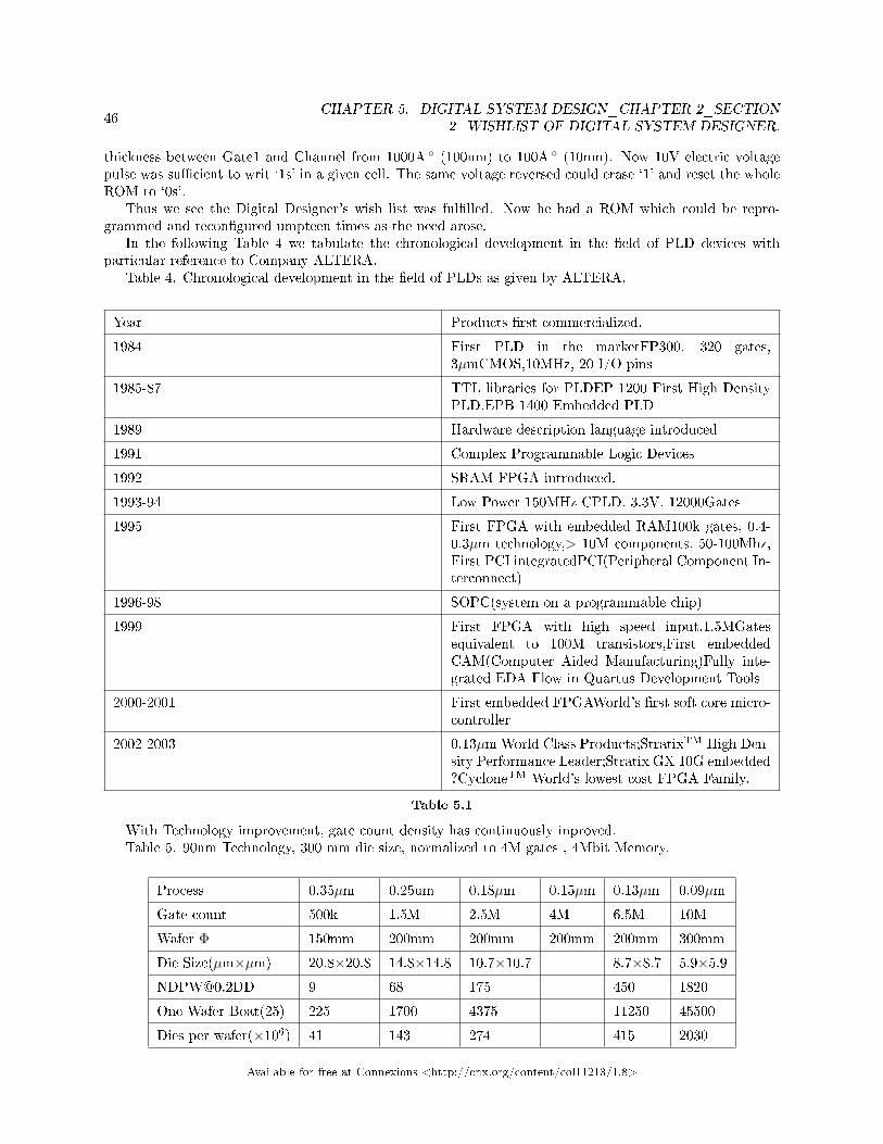
In the following Table 4 we tabulate the chronological development in the �eld of PLD devices withparticular reference to Company ALTERA.
Table 4. Chronological development in the �eld of PLDs as given by ALTERA.
Year Products �rst commercialized.
1984 First PLD in the marketFP300, 320 gates,3µmCMOS,10MHz, 20 I/O pins
1985-87 TTL libraries for PLDEP 1200 First High DensityPLD.EPB 1400 Embedded PLD
1989 Hardware description language introduced
1991 Complex Programmable Logic Devices
1992 SRAM FPGA introduced.
1993-94 Low Power 150MHz CPLD, 3.3V, 12000Gates
1995 First FPGA with embedded RAM100k gates, 0.4-0.3µm technology,> 10M components, 50-100Mhz,First PCI integratedPCI(Peripheral Component In-terconnect)
1996-98 SOPC(system on a programmable chip)
1999 First FPGA with high speed input.1.5MGatesequivalent to 100M transistors,First embeddedCAM(Computer Aided Manufacturing)Fully inte-grated EDA Flow in Quartus Development Tools
2000-2001 First embedded FPGAWorld's �rst soft core micro-controller
2002-2003 0.13µmWorld Class Products;StratixTM High Den-sity Performance Leader;Stratix GX 10G embedded?CycloneTM World's lowest cost FPGA Family.
Table 5.1
With Technology improvement, gate count density has continuously inproved.Table 5. 90nm Technology, 300 mm die size, normalized to 4M gates , 4Mbit Memory.
Process 0.35µm 0.25um 0.18µm 0.15µm 0.13µm 0.09µm
Gate count 500k 1.5M 2.5M 4M 6.5M 10M
Wafer Φ 150mm 200mm 200mm 200mm 200mm 300mm
Die Size(µm×µm) 20.8×20.8 14.8×14.8 10.7×10.7 8.7×8.7 5.9×[email protected] 9 68 175 450 1820
One Wafer Boat(25) 225 1700 4375 11250 45500
Dies per wafer(×106) 41 143 274 415 2030
Available for free at Connexions <http://cnx.org/content/col11213/1.8>

47
Table 5.2
Figure 5.3
Figure 13. The Wafer Size, Technology used and Gates realized.In Table 5 for calculating the number of dies per wafer we use the following equation taken from connexions
module m33385, Part-9_Journey of IC Technology:
Figure 5.4
� (
Figure 5.5
Available for free at Connexions <http://cnx.org/content/col11213/1.8>

48CHAPTER 5. DIGITAL SYSTEM DESIGN_CHAPTER 2_SECTION
2_WISHLIST OF DIGITAL SYSTEM DESIGNER.
Figure 5.6
Figure 14. Sectoral Composition of $173.6b sales estimate by Altera in 2003 in terms of Consumption.
Available for free at Connexions <http://cnx.org/content/col11213/1.8>

49
Figure 5.7
Figure 15. Sectoral Composition of $173.6b sales estimate by Altera in 2003 in terms of Function.As shown in Figure 16 , Programmable Array Logic (PAL) is formed from a programmable AND and
�xed OR array.
Available for free at Connexions <http://cnx.org/content/col11213/1.8>

50CHAPTER 5. DIGITAL SYSTEM DESIGN_CHAPTER 2_SECTION
2_WISHLIST OF DIGITAL SYSTEM DESIGNER.
Figure 5.8
Figure 16. Programmable Array Logic (PAL) formed from programmable AND Array and �xed ORArray.
We see in Figure 16 all intersections on decoder side that is on AND array side are shorted. By applying10V Voltage pulse as we did in EEPROM, the NMOS can be disabled. The rest shorts are retained. Sincehere we have full options for removing the shorts we say that AND Array is programmable.
On the encoder side we have no such option. Some intersections are shorted and remaining are keptopen. Here the OR Array is �xed. User has no options.
In Figure 17, we have Programmable Logic Arrays.
Available for free at Connexions <http://cnx.org/content/col11213/1.8>

51
Figure 5.9
Figure 17. Programmable Logic Array. Both AND array and OR array are programmable.As seen in the �gure, on decoder as well as encoder side all intersections are shorted. User can remove the
short on the AND array side(decoder side) as well as on OR array side(encoder side) according to his Booleanfunction requirement. Hence we say that AND array is programmable as well as OR array is programmable.
This PLA became the basis of SPLD, CPLD and FPGA.References: � Microelectronics� by Millman & Grabel, McGraw Hill, 1988.�Principles of Digital Systems Design using VHDL�, by Roth and John, CENGAGE Learning, 1998.
Available for free at Connexions <http://cnx.org/content/col11213/1.8>

52CHAPTER 5. DIGITAL SYSTEM DESIGN_CHAPTER 2_SECTION
2_WISHLIST OF DIGITAL SYSTEM DESIGNER.
Available for free at Connexions <http://cnx.org/content/col11213/1.8>

Chapter 6
DSD_Chapter 3_VHDL._introduction
and content1
VHDL(VHSICHardware Description Language)VHSIC- very high speed IC.Contents
• VHDL: An Introduction• Why VHDL• Characteristics• Basic Structure• Data Objects• Data Types• Combinational Logic Statements• Sequential Logic Statements• Concurrent Statements• Function• Procedure• Packages• Con�gurations
Introduction and overview.American Defence Department initiated the development of VHDL in 1980s for a standardized method of
describing electronic systems. By 1987 IEEE standardized VHDL in reference manual by the name of �IEEEVHDL Language Reference Manual Draft Standard version 1076/B� and was rati�ed in December 1987 asIEEE 1076-1987. VHDL is standardized for system speci�cation but not for design. VHDL is the onlyhardware language which has been standardized till date. It supports modeling and simulation of digitalsystems at various levels of design abstraction.
VHDL codes synthesis and simulation.VHDL has been made technology independent. It can always be modi�ed to add new functions. VHDL
supports the following features:
i. Hierarchies (block diagrams);ii. Reusable components;iii. Error management and veri�cations;iv. Graphical input which automatically translates into Structural VHDL;
1This content is available online at <http://cnx.org/content/m34974/1.1/>.
Available for free at Connexions <http://cnx.org/content/col11213/1.8>
53

54 CHAPTER 6. DSD_CHAPTER 3_VHDL._INTRODUCTION ANDCONTENT
v. Concurrent and sequential language constructs;vi. Speci�cation to gate description;
The codes written for a VHDL can be veri�ed in simulator by writing the test bench. Here input time signalsare given and output response signals are obtained. Thus we obtain the functional veri�cation. At a laterstage time veri�cation of the design is also possible.
Since VHDL is standardized hence , codes can be moved between di�erent development systems formodeling(simulation). These standardized codes can be synthesized by the following tools:
i. ViewLogic;ii. Mentor Graphics;iii. Synopsys.
There is no standardized language for Analog Electronics. But this standardization is in progress by thename AHDL.
Bene�ts
• Executable speci�cation• Validate spec in system context (Subcontract)• Functionality separated from implementation• Simulate early and fast (Manage complexity)• Explore design alternatives• Get feedback (Produce better designs)• Automatic synthesis and test generation (ATPG for ASICs)• Increase productivity (Shorten time-to-market)• Technology and tool independence (though FPGA features may be unexploited)• Portable design data (Protect investment)
Study of VHDL.Its characteristics are:
1. Abstraction;2. Modularity;3. Concurrency;4. Hierarchy.
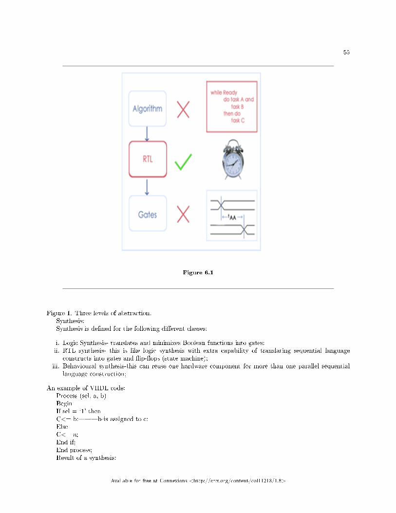
ABSTRACTION.When considering the application of VHDL to FPGA/ASIC design, VHDL can be used to describe
electronic hardware at many di�erent levels of abstracton. There are three levels of abstraction:
1. Algorithm- these are unsynthesizables;2. Register Transfer Level(RTL)-this is the input to synthesis;3. Gate level- output from synthesis.
Available for free at Connexions <http://cnx.org/content/col11213/1.8>
55
Figure 6.1
Figure 1. Three levels of abstraction.Synthesis:Synthesis is de�ned for the following di�erent classes:
i. Logic Synthesis- translates and minimizes Boolean functions into gates;ii. RTL synthesis- this is like logic synthesis with extra capability of translating sequential language
constructs into gates and �ip-�ops (state machine);iii. Behavioural synthesis-this can reuse one hardware component for more than one parallel sequential
language construction;
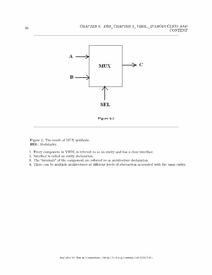
An example of VHDL code:Process (sel, a, b)BeginIf sel = `1' thenC<= b;���b is assigned to c;ElseC<= a;End if;End process;Result of a synthesis:
Available for free at Connexions <http://cnx.org/content/col11213/1.8>
56 CHAPTER 6. DSD_CHAPTER 3_VHDL._INTRODUCTION ANDCONTENT
Figure 6.2
Figure 2. The result of MUX synthesis.HDL: Modularity.
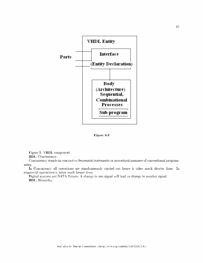
1. Every component in VHDL is referred to as an entity and has a clear interface.2. Interface is called an entity declaration.3. The �internals� of the component are referred to as architecture declaration.4. There can be multiple architectures at di�erent levels of abstraction associated with the same entity.
Available for free at Connexions <http://cnx.org/content/col11213/1.8>
57
Figure 6.3
Figure 3. VHDL componentHDL: Concurrency.Concurrency stands in contrast to Sequential statements or procedural manners of conventional program-
ming.In Concurrency all operations are simultaneously carried out hence it takes much shorter time. In
sequential operations it takes much longer time.Digital systems are DATA Driven. A change in one signal will lead to change in another signal.HDL: Hierarchy.
Available for free at Connexions <http://cnx.org/content/col11213/1.8>

58 CHAPTER 6. DSD_CHAPTER 3_VHDL._INTRODUCTION ANDCONTENT
Figure 6.4
Figure 4. Behavioral description and structural description of the entity.Bottom to top design in coding.Top to bottom design in design speci�cation.Basic Building Blocks of VHDL.
1. Library- It consists of several library units, each of which is compiled and saved in a design Library.1164 package of IEEE Standard library is used for all design purposes.
2. Entity- describes the interface(input, output, signal) of a component.3. Architecture- its internal implementations.4. Package- de�nes global information that can be used by many entities..5. Con�gurations- it binds component instances of a structure design into architecture pairs. It allows a
designer to experiment with di�erent variations of a design by selecting di�erent implementations.
Entity Declaration.The entity declaration provides an external view of a component but does not provide information about
how a component is implemented. The syntax is:Entity adder is[generic(generic_declaration);][port (A, B : in std_logic;Sum, carryover: out std_logic);]{entity_declarative_items{constants, types, signals};}End [adder][ ]: square bracket denotes optional parameters| ; vertical bar indicates a choice among alternatives.{ } : a choice of none, one or more items can be made.ENTITY DECLARATION.
Available for free at Connexions <http://cnx.org/content/col11213/1.8>

59
Figure 6.5
Figure 5. Block Diagram of Full Adder.We have a full adder as a component.a0, b0, cin are input ports and data type BIT.Sum and cout are output ports and again data type BIT.VHDL description is the following:Entity FULL_ADDER isPort( A0, B0, CIN: in std_logic;SUM, COUT:out std_logic);End FULL_ADDER;GENERIC DECLARATION:This declares constants that can be used to control the structure or behavior of the entity.Generic(constant_name:type[:=initial value]{;constant_name:type[:=initial_value]});Constant_name speci�es the name of a generic constant;Type speci�es the data type of the constant;Initial _value speci�es an initial value for the constant.VHDL is not case sensitive.Port Declaration:Port(Port_name:[mode] type[:=init_value]{;port_NAME:[MODE] TYPE[:=INIT_VALUE]});`MODE' SPECIFIES THE DIRECTION OF A PORT SIGNAL;`TYPE' SPECIFIES THE DATA TYPE;Types of Ports:There are four port modes:
1. In :can only read. It is on the right side of assignment. It is used for input only.
Available for free at Connexions <http://cnx.org/content/col11213/1.8>

60 CHAPTER 6. DSD_CHAPTER 3_VHDL._INTRODUCTION ANDCONTENT
2. Out :can only be assigned a value. It is on the left side of assignment.3. Inout :can be read and assigned a value. It can have more than one driver. It can be on both sides of
the assignment.4. Bu�er : can be read and assigned a value but it has only one driver.
Inout is bidirectional port whereas bu�er is unidirectional.The entity_declarative _item declares some constants, types or signals that can be used in the imple-
mentation of the entity.Example:Entity example_program isPort( A:in std_logic;B:in std_logic;C:out std_logic;D:inout std_logic;E:bu�er std_logic);End assign;Architecture arch_example_program of example_program isBeginProcess(A,B)BeginC<=A; �-this is valid. Input value can be assigned to output.A<=B;��not valid. A is input port so it cannot be assigned a value.E<=D+1;��this is valid. Value is read from D and assigned to E.D<=C+1;�-not valid . C is output port so you cannot read a value from C . You can only assign a
value to C.End process;End assign;ENTITY DECLARATION EXAMPLEWe can control the structure and timing of an entity using generic constants. For example in an adder
we add two BCD. Depending on the word length of BCD, adder will have to be chosen. If BCD is 4-bit widethen both inputs of Adder named A and B will not be a standard in std_logic. Instead it will be 4-bit wide�in std_logic_vector(3 downto 0)�. Also a constant N will have to declared which will give the word size.
Entity ADDER isGeneric( N: INTEGER:=4;M:TIME:= 10 ns);Port( A,B:in std_logic_vector(N-1 downto 0);CIN:in std_logic;SUM:out std_logic_vector(N-1 downto 0);COUT:out std_logic);End ADDER;ARCHITECTUREAn architecture provides an �internal� view of an entity. An entity may have more than one architecture.
It de�nes the relationships between inputs and outputs of a design entity which may be expressed in termsof:
1. Behavioural style;2. Data�ow style;3. Structural style.
An architecture determines the function of an entity. It consists of a declaration section where�signals, types, constants, components and sub-programs� are declared followed by a collection of con-
current statements.
Available for free at Connexions <http://cnx.org/content/col11213/1.8>

61
Behavioral Style Architecture.This provides the behavior but no details as to how design hardware is to be implemented. The primary
unit of a behavior description in VHDL is the process.Example:Architecture BEHAVIOUR of FULL_ADDER isBeginProcess(A, B, CIN)BeginIf (A= `0' and B= `0' and CIN= `0') thenSUM<= `0';COUT<= `0';Elsif (A= `0' and B= `0' and CIN= `1') or(A= `0' and B= `1' and CIN= `0') or(A= `1' and B= `0' and CIN= `0') thenSUM<= `1';COUT<= `0';Elsif (A= `0' and B= `1' and CIN= `1') or(A= `1' and B= `1' and CIN= `0') or(A= `1' and B= `0' and CIN= `1') thenSUM<= `0';COUT<= `1';Elsif (A= `1' and B= `1' and CIN= `1')SUM<= `1';COUT<= `1';End if;End process;End behavior;DATAFLOW STYLE ARCHITECTURE.A data�ow style speci�es a system as a concurrent representation of the �ow of control and movement of
data. It models the information �ow or data�ow over time of combinational logic functions such as adders,comparators, decoders and primitive logic gates.
Example:Architecture DATAFLOW of FULL_ADDER isSignal S: BIT;BeginS<= A xor B;SUM <= S xor CIN after 10 ns;COUT<= (A and B) or (S and CIN) after 5 ns;End DATAFLOW;[Recall in ADDER: SUM = AxorBxorCIN ;COUT= A.B+A.Cin+B.CinA.B+S.Cin = A.B +(AB′ +A′B)Cin. This reduces to A.B + A.Cin+B.Cin ]STRUCTURAL STYLE ARCHITECTURE.This gives the structural implementation using component declarations and component instantiations.In this example two types of components are de�ned: HALF_ADDER and OR_GATE. A
FULL_ADDER is implemented using two HALF_ADDERS. HALF_ADDER will be used as a compo-nent and later instantiated in a top entity of the program. Here we use our previous knowledge of buildingFA from HA.
Example:Architecture STRUCTURE of FULL_ADDER isComponent HALF_ADDER
Available for free at Connexions <http://cnx.org/content/col11213/1.8>

62 CHAPTER 6. DSD_CHAPTER 3_VHDL._INTRODUCTION ANDCONTENT
Port (L1, L2 : in BIT;CARRY, SUM : out BIT );End component;Component OR_GATEPort ( L1, L2: in BIT;O: out BIT);End component;Signal N1, N2, N3: BIT;BeginHA1: HALF_ADDER port map (A, B, N1, N2);HA2:HALF_ADDER port map (N2, CIN, N3, SUM);OR1: OR_GATE port map (N1, N3, COUT);End STRUCTURE;
Figure 6.6
Figure 6. Structural Style Architecture of Full Adder.This does not use process. By assigning the correct port map the components get instantiated into
Full_Adder.DATA OBJECTS.Data Object hold a value of speci�c type. There are three classes of data object namely:
Available for free at Connexions <http://cnx.org/content/col11213/1.8>

63
1. Constants;2. Variables;3. Signals.
The class is speci�ed by a reserved word that appears at the beginning of the declaration of that object.CONSTANTS.It is a Data Object which is initialized to a speci�c value when it is created and which cannot be
subsequently modi�ed. Constant declarations are allowed in packages, entities, architectures, subprograms,blocks and processes.
Constant YES: BOOLEAN :=True;Constant CHAR7: BIT_VECTOR(4 downto 0) :=�00111�;Constant MSB : INTEGER:= 5;VARIABLES.These data objects hold temporary data. They can be declared in a process or a subprogram.Variable X, Y: std_logic;Variable TEMP: std_logic_vector(8 downto 0);Variable DELAY: INTEGER range 0 to 15:= 5;________initial value is 5SIGNALS.Signals connect design entities together and communicates changes in values between processes. They
can be interpreted as wires or buses in actual circuit. Signals can be declared in packages (global signals),entities (entity global signals), architectures ( architecture global signals) and blocks.
Signal BEEP: std_logic :='0';Signal TEMP: std_logic_vector(8 downto 0);Signal COUNT: INTEGER range 0 to 100:=5;DATA TYPES:Data object must de�ned with a data type and the range of values it can assume.Type declarations are allowed in package declaration sections, entity declaration sections, architecture
declaration sections, subprogram declaration sections and process declaration sections.Data type include:
1. Enumeration types;2. Integer types;3. Prede�ned VHDL data types;4. Array Types;5. Record types;6. STD_LOGIC data type ;7. Signed and unsigned data types;8. Subtypes.
Enumeration TypesInteger typesVHDL Data typesArray TypesRecord TypesStd_logic typesSigned and unsigned data types.Subtypes.LOGICAL OPERATORSLogical operators are � AND, OR,NAND, NOR, XOR and NOT� accept operands of same type and same
length.Type of OPERANDS can be � BIT, BOOLEAN or ARRAY�.Example:
Available for free at Connexions <http://cnx.org/content/col11213/1.8>

64 CHAPTER 6. DSD_CHAPTER 3_VHDL._INTRODUCTION ANDCONTENT
Signal A, B : BIT_VECTOR (6 downto 0);Signal C,D,E,F,G: BIT;A<= B and C;��-not allowed because types are incompatible.D<=(E xor F) and (C xor G);����� this is a valid statement.RELATIONAL OPERATORSRelational Operators give a result of Boolean type. Operands must be of same type ad length.Example;Signal A,B: BIT_VECTOR(6 downto 0);Signal C: BOOLEAN;C<= B <= A;(same as C<=(B<=A);)COMBINATIONAL LOGIC STATEMENTS.
1. Data�ow type(logical operation, arithmetic operations);2. When else statement;3. With select statement.
Example:Architecture arch_andgate of andgate isBeginY<= `1' when A = �1' and B = `1'Else `0';End arch_andgate;With �a, b� selectY<= �X X� when �1 1�SEQUENTIAL STATEMENTSThe statements within a process may be sequential but the process may be concurrent.VARIABLE ASSIGNMENT STATEMENTS.The current value of a variable is replaced with a new value speci�ed by the expression. The variable
and the result of the expression must be the same type and same length.Target_variable:= expression;Variables declared within a process cannot pass values outside the process.Example:Process(S1,S2)Variable A, B : INT16;Constant C: INT16:=100;BeginA:=S1+1;B:=S2*2-C;End process;Signal Assignment StatementsTarget_signal<= [transport] expression [ after time_expression];Assignment will not take place immediately. There can be two kinds of delays that can be applied when
scheduling signal assignments:
1. Transport delay- analogous to propagation delay;2. Inertial delay � the input must persist for sometime before output responds. This is very useful for
rejecting the input glitches which are very short interval signals.
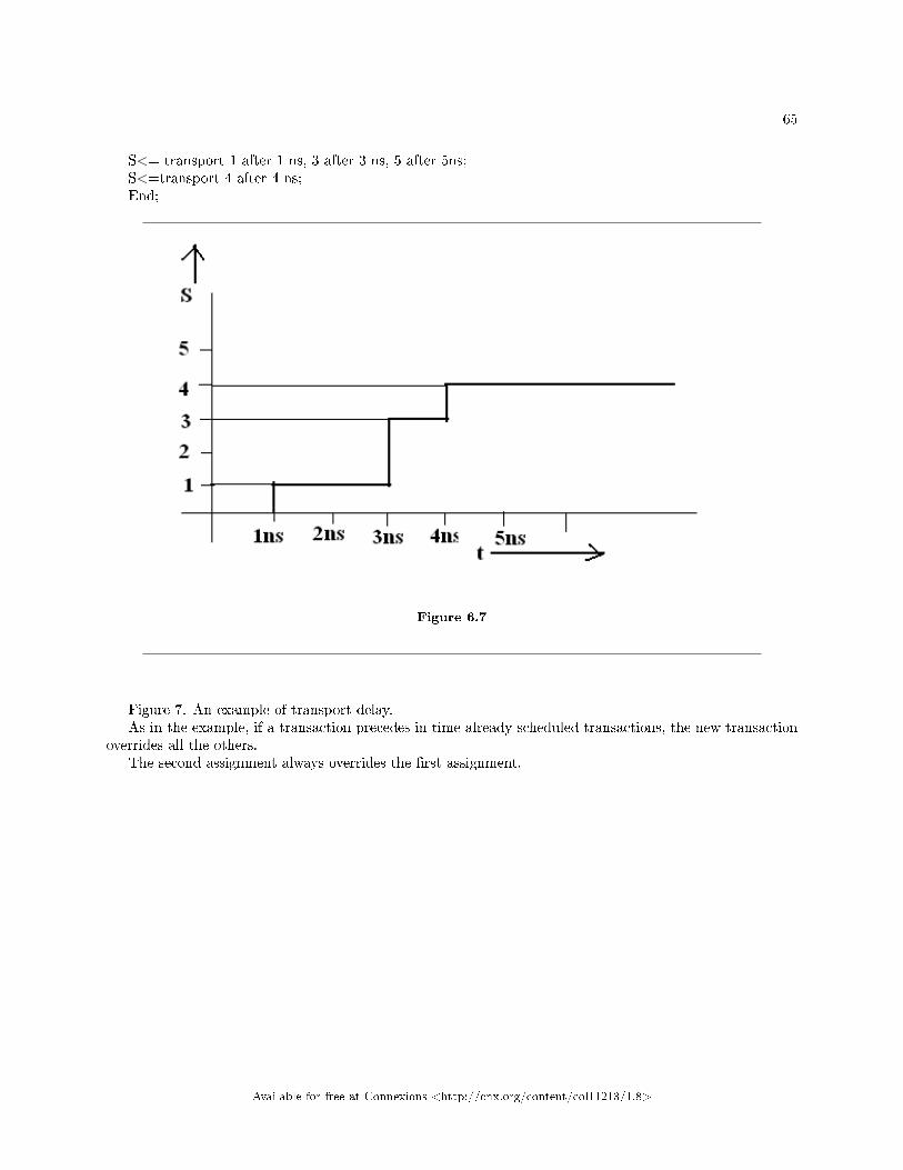
TRANSPORT DELAY.. . .. . .Process(. . ...)Begin
Available for free at Connexions <http://cnx.org/content/col11213/1.8>
65
S<= transport 1 after 1 ns, 3 after 3 ns, 5 after 5ns;S<=transport 4 after 4 ns;End;
Figure 6.7
Figure 7. An example of transport delay.As in the example, if a transaction precedes in time already scheduled transactions, the new transaction
overrides all the others.The second assignment always overrides the �rst assignment.
Available for free at Connexions <http://cnx.org/content/col11213/1.8>

66 CHAPTER 6. DSD_CHAPTER 3_VHDL._INTRODUCTION ANDCONTENT
Figure 6.8
Figure 8. Distinction between Inertial and transport case.As we see in the above example, Inertial Model; does not allow the glitches to appear at the output but
in transport model it does appear.Zero Delay vs Delta Delay.Variable assignments are executed in zero time. However VHDL uses delta time concept for signal
assignments. Each signal assignment statement is executed after a delta time.process (CLK)signal A : integer := 5 ;B, C : integer := 0 ;variable D : integer := 0 ;beginA <= 1;A <= 2;B <= A;D := 3;C <= D;end process ;
Available for free at Connexions <http://cnx.org/content/col11213/1.8>

67
Figure 6.9
Figure 9. The timing diagram of the Process described in the text.The process is activated by any change in the CLK signal. The CLK changes in zero time. 0- and
0+ are both 0 for a simulator. The interval, two delta (2D) is a virtual concept. A signal assignment isexecuted after a delta delay however variable assignments are executed in zero time. The �rst assignmentis a signal assignment, therefore A will be assigned �1� after a delta time. The second assignment is also asignal assignment so A will be �2� after two delta time. Third assignment assigns signal B, the initial valueof A (the value at 0- time) because delta time concept is virtual. So B takes �5� after a delta time. Fourthassignment is a variable assignment, so it will be executed without delta delay. The last assignment is againa signal assignment ; signal C takes the value of D after a delta time. Since D is �3� at zero time C isassigned to �3�.
This is why signal assignments should be avoided in processes. If we de�ne signal A as a variable B takesthe value of �2� .
IF STATEMENTS.Example:Signal A,B, IN1, Y: std_logic;Process (A,B)BeginIf A= `1' AND B = `1' thenY<= `0';Elsif IN1= `1' thenY<= `1';Else Y <= `0';End if;End process;CASE STATEMENTS.This selects one of a number of alternative sequence of statements. The chosen alternative is de�ned by
the value of an expression.
Available for free at Connexions <http://cnx.org/content/col11213/1.8>

68 CHAPTER 6. DSD_CHAPTER 3_VHDL._INTRODUCTION ANDCONTENT
Example:Signal S1: INTEGER range 0 to 7;Signal I1, I2, I3 : BIT;Process (S1, I1,I2,I3)BeginCase S1 isWhen 0|2 =>OU<= `0';When 1 =>OU<= I1;When 3 to 5 =>OU<=I2;When others =>OU<= I3;End case;End process;LOOP STATEMENTS.A repeated process is put into LOOP STATEMENT.There are two loops:FOR Loop and WHILE Loop.If LOOP not used and repetitive statement is used then we use WAIT and EXIT STATEMENTS.Example of two nested loops without iteration.Count_down: processVariable min, sec : integer range 0 to 60;BeginL1: loopL2: loopExit L2 when (sec=0);Wait until CLK'event and CLK = `1';Sec := sec-1; ���every decrement takes place at the leading edge of the CLOCK.End loop L2;ExitL1 when (min = 0);Min:= min � 1;Sec := 60;End loop L1;End process count_down;FOR loop statements.This iterates over a number of values. The loop index is integer value by default.It can be reassigned a value within the loop.Example:For i in 1 to 10 loopA(i) := i*I;End loop;For I in X downto Y loopA(I) := i*i;End loop;WHILE Loop Statements.A WHILE LOOP executes the loop body by �rst evaluating the condition. If the condition is true the
loop is executed.Example:Process
Available for free at Connexions <http://cnx.org/content/col11213/1.8>

69
Variable a, b, c, d : integer;Begin. . .. . .. . .. . .. . .. . .. . .While ((a+b)>(c+d)) loopA :=a-1;C:=c+b;B := b � d;End loop;. . .. . .. . .. . ...End process;NULL STATEMENTS.This statement is used to explicitly state that no action is to be performed when a condition is true.Example:Variable A,B:INTEGER range 0 to 31;Case A isWhen 0 to 12 =>B := A;When others =>Null;End case;Assertion Statements.Next StatementExit Statement.Wait Statement.Procedure Statement.Concurrent Statement.Process Statement.A process statement is composed of sequential statements but processes themselves are concurrent.The process statement must have either a sensitivity list or a wait statement or both.Example.Architecture A2 of example isSignal i1, i2, i3 , i4, and_out, or_out : bit;BeginPr1: process(i1, i2, i3, i4)BeginAnd_out<= i1 and i2 and i3 and i4;End process pr1;Pr2: process(i1,i2,i3,i4)BeginOr_out<= i1 or i2 or i3 or i4;End process pr2;End A2;Concurrent Signal assignments.Conditional Signal Assignments.Block Statements.Block Statement.Example: Block B1-1 is nested within block B1. Both B1 and B1-1 declare a signal named S. The signal
S used in Block B1-1 will be the one declared within B1-1 while S is used in block B2 is the one declared inB1.
Architecture BHV of example isSignal out1: integer;
Available for free at Connexions <http://cnx.org/content/col11213/1.8>
70 CHAPTER 6. DSD_CHAPTER 3_VHDL._INTRODUCTION ANDCONTENT
Signal out2: bit;BeginB1: blockSignal S : bit;BeginB1-1: blockSignal S: integer;BeginOut1<= S;End block B1-1;End block B1;B2: blockBeginOut2<= S;End block B2;End BHV.Concurrent Procedure CallSub programs
1. Procedure;2. Functions.
FUNCTIONSExample:ProcessFunction c_to_f(c:real) return real is variable f: real;BeginF:c*9.0/5.0+32.0;Return(f);End c_to_f;Variable temp: real;BeginTemp:= c_to_f(5.0)+20.0;(temp=61)End process;Here class of a object refers to constant or signal and the mode is `in'. Default value of MODE is `in'.
Default value of CLASS is `constant'.PROCEDURESProcedure parity(A: in bit_vector(0 to 7);Result1, result2:out bit)isVariable temp:bit;BeginTemp:= `0';For I in 0 to 7 loopTemp:= temp xor A(I);End loop;Result1:= temp;Result2:= not temp;End;Here by default result1 and result2 will be classi�ed as VARIABLE.Example 2.Architecture BHV of receiver isBegin
Available for free at Connexions <http://cnx.org/content/col11213/1.8>

71
ProcessVariable TOP,BOTTOM,ODD,dummy:bit;Varable y: bit_vector (15 downto 0);Begin..Parity(y(15 downto 8), TOP, dummy);Parity(y(7 downto 0), BOTTOM, dummy);ODD:= TOP xor BOTTOM;End process;End BHV;PACKAGES.The package body speci�es the actual behavior of the package. It has the same name as the declaration.Example>Library IEEE;Use IEEE.NUMERIC_BIT.all;Package PKG isSubtype MONTHY_TYPE is integer range 0 to 12;Subtype DAY_TYPE is integer range 0 to 31;Subtype BCD4_Type is unsigned (3 downto 0);Subtype BCD5_Type is unsigned ( 4 downto 0);Constant BCD5_1: BCD5_TYPE := B*0_0001�;Constant BCD5_7: BCD5_TYPE := B*0_0111�;Function BCD_INC(L: in BCD4_TYPE)return BCD5_TYPE;End PKG;Package body PKG isFunction BCD_INC(L: in BCD4_TYPE)return BCD5_TYPE isVariable V,V1,V2: BCD5_TYPE;BeginV1:= L+BCD5_1;V2:=L+BCD5_7;Case V2(4) isWhen `0' => V:=V1;When `1' => V:=V2;End case;Return (V);End BCD_INC;End PKG;GENERATE STATEMENT.The generate statement is a concurrent statement that has to be de�ned in an architecture. It is used to
describe replicated structures. The syntax is :instantiation_label : generation_scheme generate{concurrent_statement}end generate [instantiation_label ] ;There are two kinds of generation_scheme : the for scheme and the if scheme. A for scheme is used to
describe a regular structure. It declares a generate parameter and a discrete range just as the for_schemewhich de�nes a loop parameter and a discrete range in a sequential loop statement. The generate parameterneeds not to be declared. Its value may be read but cannot be assigned or passed outside a generatestatement.
Example:Architecture IMP of FULL_ADDER4 is
Available for free at Connexions <http://cnx.org/content/col11213/1.8>
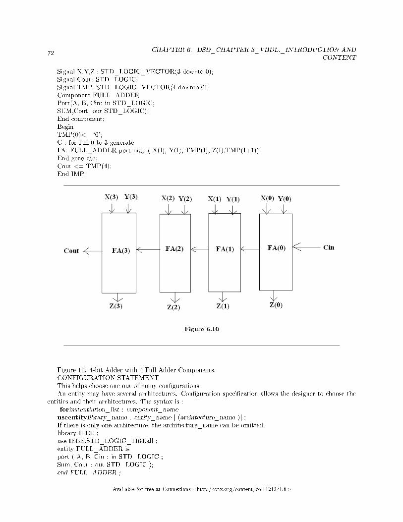
72 CHAPTER 6. DSD_CHAPTER 3_VHDL._INTRODUCTION ANDCONTENT
Signal X,Y,Z : STD_LOGIC_VECTOR(3 downto 0);Signal Cout: STD_LOGIC;Signal TMP: STD_LOGIC_VECTOR(4 downto 0);Component FULL_ADDERPort(A, B, Cin: in STD_LOGIC;SUM,Cout: out STD_LOGIC);End component;BeginTMP(0)<= `0';G : for I in 0 to 3 generateFA: FULL_ADDER port map ( X(I), Y(I), TMP(I), Z(I),TMP(I+1));End generate;Cout <= TMP(4);End IMP;
Figure 6.10
Figure 10. 4-bit Adder with 4 Full Adder Components.CONFIGURATION STATEMENTThis helps choose one out of many con�gurations.An entity may have several architectures. Con�guration speci�cation allows the designer to choose the
entities and their architectures. The syntax is :forinstantiation_list : component_nameuseentitylibrary_name . entity_name [ (architecture_name )] ;If there is only one architecture, the architecture_name can be omitted.library IEEE ;use IEEE.STD_LOGIC_1164.all ;entity FULL_ADDER isport ( A, B, Cin : in STD_LOGIC ;Sum, Cout : out STD_LOGIC );end FULL_ADDER ;
Available for free at Connexions <http://cnx.org/content/col11213/1.8>
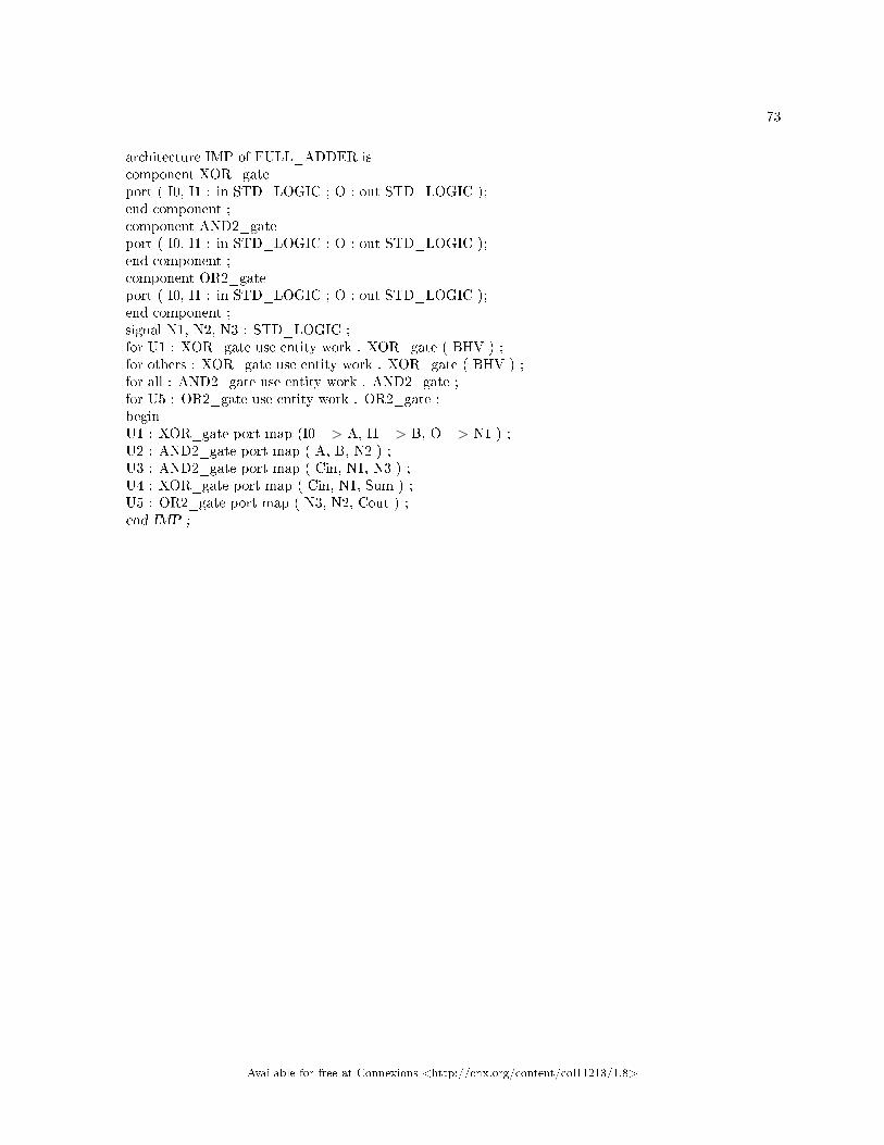
73
architecture IMP of FULL_ADDER iscomponent XOR_gateport ( I0, I1 : in STD_LOGIC ; O : out STD_LOGIC );end component ;component AND2_gateport ( I0, I1 : in STD_LOGIC ; O : out STD_LOGIC );end component ;component OR2_gateport ( I0, I1 : in STD_LOGIC ; O : out STD_LOGIC );end component ;signal N1, N2, N3 : STD_LOGIC ;for U1 : XOR_gate use entity work . XOR_gate ( BHV ) ;for others : XOR_gate use entity work . XOR_gate ( BHV ) ;for all : AND2_gate use entity work . AND2_gate ;for U5 : OR2_gate use entity work . OR2_gate ;beginU1 : XOR_gate port map (I0 => A, I1 => B, O => N1 ) ;U2 : AND2_gate port map ( A, B, N2 ) ;U3 : AND2_gate port map ( Cin, N1, N3 ) ;U4 : XOR_gate port map ( Cin, N1, Sum ) ;U5 : OR2_gate port map ( N3, N2, Cout ) ;end IMP ;
Available for free at Connexions <http://cnx.org/content/col11213/1.8>

74 CHAPTER 6. DSD_CHAPTER 3_VHDL._INTRODUCTION ANDCONTENT
Available for free at Connexions <http://cnx.org/content/col11213/1.8>

Chapter 7
DSD_Chapter 4_VHDL application to
combinatorial logic synthesis1
DSD_Chapter 4_Application of VHDL to Combinatorial SynthesisIn Chapter 3, we studied VHDL and its di�erent commands. Here we are going to write the codes for
a given combinatorial logic system which has been ordered by the customer. These codes will be used tocon�gure FPGA. That con�gured FPGA will act like the Combinatorial Logic System1 which has beenordered by my Customer.
Two design approach can be used while writing the VHDL codes for a system namely behavioral anddata-�ow design approach.
Say we have a logic function: y = a.b��and_gateIn data �ow design we write :Architecture behavioral of and_gate isBegin_________y<= a and b;end behavioral;In behavioral design approach we write:Architecture behavioral of and_gate isBegin________y<= `1' when a= `1' and b= `1' else `0';end behavioral;There is a third approach namely structural approach. This consists of interconnection of several com-
ponents known as Entity. Structural VHDL is used for hierarchical design. This is must for handling largedesign in VHDL.By large design we mean 500 to 6000 gates.
The components which are to be instanced or to be instantiated (that is to be incorporated) in a givenentity must be de�ned beforehand and their architecture behavioral must be given in their de�nition.
How to use ISE for writing the codes and checking for syntax errors?Click ISE. Project Navigator opens. Tip of the Day will come. OK it.Create a new project after clicking FILE.New Project Wizard will open.Give Project Name. . .. . .. . .ANDGate1�����You can use underscore but hyphen cannot be used.Give Project Location. . .. . . C:\BKS_Project\ANDGate1Project name: ANDGate1Top Level Source Type- HDLOther options are: Schematic,EDIF,NGC/NGO � these are higher level tools.Product Category: All (for CPLD & FPGA).
1This content is available online at <http://cnx.org/content/m34984/1.4/>.
Available for free at Connexions <http://cnx.org/content/col11213/1.8>
75

76 CHAPTER 7. DSD_CHAPTER 4_VHDL APPLICATION TOCOMBINATORIAL LOGIC SYNTHESIS
Other options are General Purpose, Automotive, Military, Hi-reliability, Radiation Hardened.Family SPARTAN2 (FPGA)Other options are QPro Virtex Hi-Rel, QPro Virtex4Hi-Rel,Q-Pro Virtex4 Rad Tolerant, QPro VirtexE
Military, Spartan3A DSP.Device : XC2S15_____Xilinx component, Spartan2,15k gate count.Other options are XC2S30,XC2S50,XC2S100,XC2S150.Package: TQ144_______no of pins 144.Other options are CS144, VQ100.Speed: -6Other options are -5, -5QTop Level Source Type: HDL.Synthesis Tool XST(VHDL/Verilog)Simulator: ModelSim � XE VHDL.Other options of Simulator are ModelSim XE Verilog,NC Sim VHDL, NC Sim Verilog, NC Sim Mixed,
VCS MX VHDL, VCS MX Verilog, VCS MX Mixed, VCS MXi Verilog.At the bottom three messages displayed:Enable Enhanced Design Summary �
√
Enable Message Filtering �Display Incremental Message �This imples that Enable Enhanced Design Summary is enabled and Enable Message Filtering+ Display
Incremental Message are disabled.Click NEXT.New page opens. New Project Wizard������-create new sources.Click New SourceFollowing options will come_____IPSchematic,State Diagram, Test Bench Waveform, User Document,
Verilog Module, Verilog Test Fixture, VHDL Module, VHDL Package, VHDL Test Bench.Creating a new source and adding to the Project is optional. Existing source can be added on the next
page.Click NEXT.Add existing source if any.Click NEXT.New Page opens called PROJECT SUMMARYProject Name: ANDGate1����������-this can contain underscore but not hyphen. ���
������������������If we include hyphen the NEW SOURCE can ���������������������never be set as TOP MODULE.
Project Path C:\documents and settings\BKS\MyDocuments\ANDGate1Top Level Source____________HDLDEVICEDevice Family_______________Spartan2Device_____________________XC2S15Package____________________TQ144Speed______________________-6Synthesis Tool________________XSTSimulator____________________ModelSim XE VHDLPreferred Language___________VHDL.Enable Enhanced Design Summary �
√
Enable Message Filtering �Display Incremental Message �Finish.Following icons will display on left margin.[U+2302] ANDGate1
Available for free at Connexions <http://cnx.org/content/col11213/1.8>
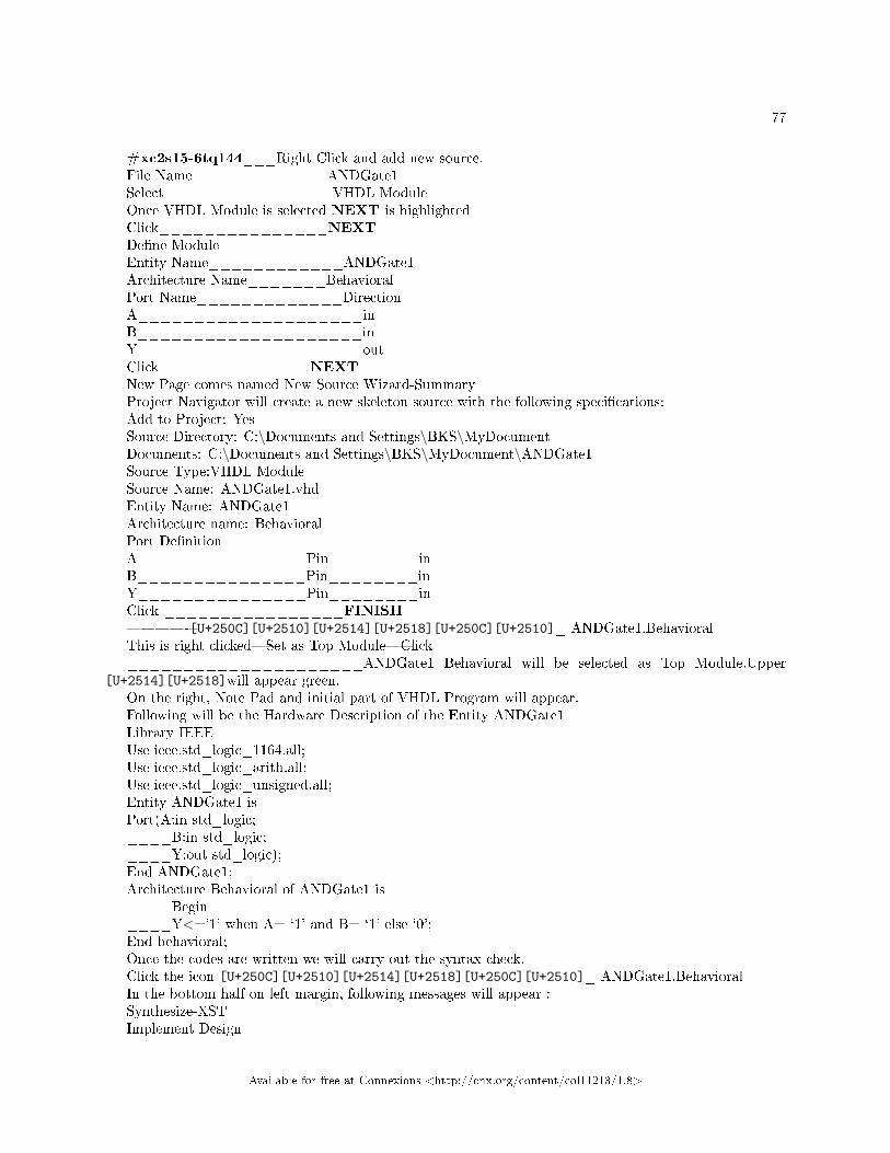
77
#xc2s15-6tq144___Right Click and add new source.File Name____________ANDGate1Select_______________VHDL ModuleOnce VHDL Module is selected NEXT is highlightedClick_______________NEXTDe�ne ModuleEntity Name____________ANDGate1Architecture Name_______BehavioralPort Name_____________DirectionA____________________inB____________________inY____________________outClick _____________NEXTNew Page comes named New Source Wizard-SummaryProject Navigator will create a new skeleton source with the following speci�cations:Add to Project: YesSource Directory: C:\Documents and Settings\BKS\MyDocumentDocuments: C:\Documents and Settings\BKS\MyDocument\ANDGate1Source Type:VHDL ModuleSource Name: ANDGate1.vhdEntity Name: ANDGate1Architecture name: BehavioralPort De�nitionA_______________Pin________inB_______________Pin________inY_______________Pin________inClick ________________FINISH����-[U+250C][U+2510][U+2514][U+2518][U+250C][U+2510]_ ANDGate1.BehavioralThis is right clicked�Set as Top Module�Click_____________________ANDGate1 Behavioral will be selected as Top Module.Upper
[U+2514][U+2518]will appear green.On the right, Note Pad and initial part of VHDL Program will appear.Following will be the Hardware Description of the Entity ANDGate1Library IEEEUse ieee.std_logic_1164.all;Use ieee.std_logic_arith.all;Use ieee.std_logic_unsigned.all;Entity ANDGate1 isPort(A:in std_logic;____B:in std_logic;____Y:out std_logic);End ANDGate1;Architecture Behavioral of ANDGate1 is____Begin____Y<='1' when A= `1' and B= `1' else `0';End behavioral;Once the codes are written we will carry out the syntax check.Click the icon [U+250C][U+2510][U+2514][U+2518][U+250C][U+2510]_ ANDGate1.BehavioralIn the bottom half on left margin, following messages will appear :Synthesize-XSTImplement Design
Available for free at Connexions <http://cnx.org/content/col11213/1.8>

78 CHAPTER 7. DSD_CHAPTER 4_VHDL APPLICATION TOCOMBINATORIAL LOGIC SYNTHESIS
Generate Programming FileCon�gure Target DeviceSave the note pad program and click Synthesize-XSTIf RED appears, synthesis has failed.We correct the program,save it and repeat syntax check until we get the messageProcess �Synthesis� completed successfully.Click the PLUS sign on the left side of Synthesize-XST+ Synthesize-XST___________# View Synthesis Report___________[U+2592] View RTL Schematic___________[U+2592] View Technology SchematicIf we click # View Synthesis Report we get the following:
1. Synthesis Options Summary.2. HDL Complilation.3. Design Hierarchy Analysis.4. HDL Analysis.5. HDL Synthesis.6. Advanced HDL Synthesis.7. Low Level Synthesis.8. Partition Report.9. Final Report:
a. Device Utilization Summary.b. Partition Report Summary.c. Timing Report.
If we click [U+2592] View RTL (Register Transfer Level) Schematic, we get to see the interface connectionsof the Entity Block.
If we click [U+2592] View Technology Schematic, we get to see the internal architecture of the entity.Now we can carry out the FUNCTIONAL VALIDATION of the given source by writing its TEST
BENCH.#xc2s15-6tq144___Right Click and add new source.File Name____________TbANDGate1Select_______________VHDL TestBenchOnce VHDL TestBench is selected NEXT is highlightedClick_______________NEXTNew Page comes named New Source Wizard- Associate SourceSelect a source(which is already de�ned) with which to associate the new source(in this case the test
bench).ANDGate1 is selected to associate with the Test Bench.Click_______________NEXTNew Source Wizard-Summary.Project Navigator will create a new skeleton source with the following speci�cations:Add to Project: YesSource Directory: C:\Documents and Settings\BKS\ANDGate1Source Type:VHDL TestBench.Source Name: TbANDGate1.vhdAssociation: ANDGate1Click ________________FINISHOn the right hand side in the Note-Pad we write the test bench program.Library IEEEUse ieee.std_logic_1164.all;
Available for free at Connexions <http://cnx.org/content/col11213/1.8>

79
Use ieee.std_logic_arith.all;Use ieee.std_logic_unsigned.all;Entity TbANDGate1 isEnd TbANDGate1;Architecture Behavioral of ANDGate1 is- - - -component declaration for the unit under test(uut).Component ANDGate1____Port(a:in std_logic;________b:in std_logic;________y:out std_logic);End component;- - - -inputs.Signal a:std_logic:= `0';Signal b:std_logic:= `0';- - - outputs.Signal y:std_logic;Begin- - - - -instantiate(or incorporate) the unit under test(UUT);uut:ANDGate1 Port Map(a => a,b => b,y => y,);- - - - - => means transpose or corresponds;- - - - - no clocks detected in port list. Replace<clocks> below with appropriate name.- - - - -constant<clock>_period:= 1 ns;- - - - -<clock>_process:process- - - - -begin- - - - -<clock> <= `0' ;- - - - -wait for <clock>_period/2;- - - - -<clock> <= `1' ;- - - - -wait for <clock>_period/2;- - - - -end process;- - - - stimulus process________stim_proc:process________begin____________wait for 10 ns;____________a<= `1';____________b<= `1';____________wait for 10 ns;____________a<= `1';____________b<= `0';____________wait for 10 ns;____________a<= `1';____________b<= `1';____________wait for 10 ns;____________a<= `1';____________b<= `0';- - - - - - - - - - -insert stimulus here_________wait;_________end process;End;Change Implementation to Behavioral Simulation.
Available for free at Connexions <http://cnx.org/content/col11213/1.8>
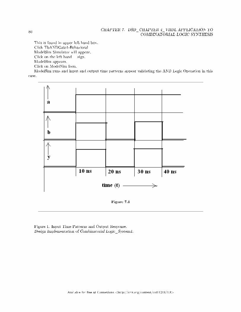
80 CHAPTER 7. DSD_CHAPTER 4_VHDL APPLICATION TOCOMBINATORIAL LOGIC SYNTHESIS
This is found in upper left hand box.Click TbANDGate1-BehavioralModelSim Simulator will appear.Click on the left hand + sign.ModelSim appears.Click on ModelSim Icon.ModelSim runs and input and output time patterns appear validating the AND Logic Operation in this
case.
Figure 7.1
Figure 1. Input Time Patterns and Output Response.Design Implementation of Combinatorial Logic_System1.
Available for free at Connexions <http://cnx.org/content/col11213/1.8>

81
Figure 7.2
Figure 2. Gate Description of Combinatorial Logic System1.
Figure 7.3
Figure 3. Interface Description of Combinatorial Logic System1Y = A.B + C(XOR)DCustomer has provided this circuit con�guration. This has to be synthesized with no syntax error. The
Synthesis has to be functionally tested. Next the masks are generated and sent to foundry.For Hardware description, we open ISE.Add source if it exists.New source if it does not exist.We select VHDL Module and save it as logic_system1. We have chosen Xilinx Component Spartan 2.I/P, O/P de�ned;We get the following two icons.
Available for free at Connexions <http://cnx.org/content/col11213/1.8>

82 CHAPTER 7. DSD_CHAPTER 4_VHDL APPLICATION TOCOMBINATORIAL LOGIC SYNTHESIS
[U+2302] Logic_system1#xc2s15-6tq144___Right Click and add new source.We need to de�ne three gates: AND_Gate, XOR_Gate and OR_Gate.Each gate will be de�ned, selected
as TOP MODULE and synthesized. Once synthesis is complete then we will move to the next new source.Finally we will synthesize LogicSystem1. Now LogicSystem1 will be synthesized by selecting it as TOPMODULE. Once the synthesis of LogicSystem1 is successful we will validate it by making its Test Bench.
After de�ning, we instantiate (or incorporate) these three gates to Logic System1.Add a new source and name it ANDgateFirst we de�ne AND_Gate:Library IEEEUse ieee.std_logic_1164.all;Use ieee.std_logic_arith.all;Use ieee.std_logic_unsigned.all;Entity AND_Gate isPort(A:in std_logic;____B:in std_logic;____Y:out std_logic);End AND_Gate;Architecture Behavioral of ANDGate1 isBeginY<= A and B;- - - - data �ow design methodEnd behavioral;Select ANDgate as TOP MODULE and do the syntax check here itself.Second we de�ne XOR_Gate by right clicking #xc2s15-6tq144 and adding a new source named
XOR_Gate.Library IEEEUse ieee.std_logic_1164.all;Use ieee.std_logic_arith.all;Use ieee.std_logic_unsigned.all;Entity XOR_Gate isPort(A:in std_logic;____B:in std_logic;____Y:out std_logic);End XOR_Gate;Architecture Behavioral of XOR_Gate isBeginY<= A xor B;- - - - data �ow design methodEnd behavioral;Here XORgate is selected as TOP MODULE and syntax check is done.Once synthesis is successful then
only proceed forward.Third we de�ne OR_Gate by right clicking#xc2s15-6tq144 and adding a new source named OR_Gate.Library IEEEUse ieee.std_logic_1164.all;Use ieee.std_logic_arith.all;Use ieee.std_logic_unsigned.all;Entity OR_Gate isPort(A:in std_logic;____B:in std_logic;____Y:out std_logic);End OR_Gate;Architecture Behavioral of OR_Gate is
Available for free at Connexions <http://cnx.org/content/col11213/1.8>

83
BeginY<= A or B;- - - - data �ow design methodEnd behavioral;Now we implement Logic_System1 (Figure 3) by interconnecting these three components. But �rst these
three Gates will have to be declared.Library IEEEUse ieee.std_logic_1164.all;Use ieee.std_logic_arith.all;Use ieee.std_logic_unsigned.all;Entity logic_system is______Port(A: in std_logic;__________B: in std_logic;__________C: in std_logic;__________D: in std_logic;__________Y: out std_logic);- - - -interface connections are declaredArchitecture arch_logic_system1 of logic_system1 is______Signal P:std_logic;______Signal Q:std_logic;______Component And_gate is- - - - -declaration of And_Gate;______________Port(A,B: in std_logic;____________________Y: out std_logic______________________);______End component;______Component Or_gate is____________Port(A,B: in std_logic;__________________Y: out std_logic___________________);______End component;______Component XOR_gate is- - - -declaration of XOR_Gate____________Port(A,B: in std_logic;___________________Y: out std_logic___________________);_______End component;Begin_______U1: And_gate port map(A,B,P);���non-named association.���-Port map(A[U+F0F3] A, B[U+F0F3]B, P[U+F0F3] Y);��-named association._______U2:XOR_gate port map(C, D, Q);_______U3:Or_gate port map (P,Q, Y);End arch_logic_sysytem1;LogicSystem1 is set as TOP MODULE and syntax check is done until SYNTHESIS is successful. Then
we add a new source TbLogicSystem1. LogicSystem1 is our UUT. Test bench is associated with UUT andModelSim is carried out. Check if you get the correct output for a given input.Once validated we can sendthe mask diagrams to the Foundry.
Implementation of Combinatorial Logic System2.
Available for free at Connexions <http://cnx.org/content/col11213/1.8>

84 CHAPTER 7. DSD_CHAPTER 4_VHDL APPLICATION TOCOMBINATORIAL LOGIC SYNTHESIS
Figure 7.4
Figure 4. Gate Description of Combinatorial Logic System2.
Figure 7.5
Figure 5. Interface Description of Combinatorial Logic_System2.
Available for free at Connexions <http://cnx.org/content/col11213/1.8>

85
Library IEEEUse ieee.std_logic_1164.all;Use ieee.std_logic_arith.all;Use ieee.std_logic_unsigned.all;Entity logic_system2 isPort(A: in std_logic;____B: in std_logic;____C: in std_logic;____D: in std_logic;____E: in std_logic;____F: in std_logic;____G: in std_logic;____Y:out std_logic);Architecture Arch_logic_system2 of logic_system2 is______Signal P: std_logic;______Signal Q: std_logic;______Signal R: std_logic;______Signal S: std_logic;______Component And_gate is____________Port(A,B: in std_logic;__________________Y:out std_logic);____________End component:______Component Or_gate is____________Port(A,B: in std_logic;__________________Y: out std_logic);____________End component;______Component NAND_gate is____________Port(A, B, C:in std_logic;____________________Y: out std_logic);____________End component;______Component NAND_gate is____________Port(A, B:in std_logic;__________________Y: out std_logic);____________End component;_______Component XNOR_gate is____________Port(A, B, C:in std_logic;____________________Y: out std_logic);____________End component;_______Begin____________U1: And_gate port map(A,B,P);____________U2: Nand_gate port map (C,D,E,Q);____________U3: XNOR_gate port map (F, G, R);____________U4:NAND_gate port map (P, Q, S);____________U5: OR _gate port map (S, R, Y);______End arch_logic_system2;For functional validation, the interconnected components will have to be de�ned,their behavioral archi-
tecture will have to be de�nedVHDL codes for AND gate.
Available for free at Connexions <http://cnx.org/content/col11213/1.8>

86 CHAPTER 7. DSD_CHAPTER 4_VHDL APPLICATION TOCOMBINATORIAL LOGIC SYNTHESIS
Figure 7.6
Figure 6. Interface Description of AND gateBehavioral Architecture of AND gate using `When' � `Else'Library IEEEUse ieee.std_logic_1164.all;Use ieee.std_logic_arith.all;Use ieee.std_logic_unsigned.all;Entity AND_gate2 is______Port (A: in std_logic;___________B: in std_logic;___________Y: out std_logic);End AND_gate2;Architecture arch_AND_gate2 of AND_gate2 isBeginY<= `1' when A= `1' and B= `1' else `0';End arch_AND-gate2;Behavioral Architecture of AND gate using `If'- `Then' � `Else'Library IEEEUse ieee.std_logic_1164.all;Use ieee.std_logic_arith.all;Use ieee.std_logic_unsigned.all;Entity AND_gate3 is______Port (A: in std_logic;__________B: in std_logic;__________Y: out std_logic);End AND_gate3;Architecture arch_AND_gate of AND_gate3 is______Begin__________Process (A, B)__________begin__________if A = `1' and B = `1' then Y<= `1�;__________else Y <= `0';__________end if;__________End process;End arch_AND_gate;Behavioral Architecture of OR gate using `When' � `Else'
Available for free at Connexions <http://cnx.org/content/col11213/1.8>

87
Figure 7.7
Figure 7. Interface Description of OR Gate.Library IEEEUse ieee.std_logic_1164.all;Use ieee.std_logic_arith.all;Use ieee.std_logic_unsigned.all;Entity OR_gate is______Port (A: in std_logic;___________B: in std_logic;___________Y: out std_logic);End OR_gate;Architecture behavioral of OR_gate isBegin_____Y<= `0' when A= `0' and B= '0' else `1';End behavioral;Behavioral Architecture of XNOR gate using `If'- `Then' � `Else'
Figure 7.8
Figure 8. Interface Description of XNOR gate.Library IEEEUse ieee.std_logic_1164.all;Use ieee.std_logic_arith.all;Use ieee.std_logic_unsigned.all;
Available for free at Connexions <http://cnx.org/content/col11213/1.8>

88 CHAPTER 7. DSD_CHAPTER 4_VHDL APPLICATION TOCOMBINATORIAL LOGIC SYNTHESIS
Entity XNOR_gate is_______Port (A: in std_logic;____________B: in std_logic;____________Y: out std_logic);End XNOR_gate;Architecture behavioral of XNOR_gate isBegin______Process(A, B)______Begin______If A = B then Y<= `1';______else Y<= `0';������Equality gate or even parity gate______end if;______end process;End behavioral;Behavioral Architecture of XOR gate using `When' � `Else'
Figure 7.9
Figure 9. Interface description of XOR gate.Library IEEEUse ieee.std_logic_1164.all;Use ieee.std_logic_arith.all;Use ieee.std_logic_unsigned.all;Entity XOR_gate is______Port (A: in std_logic;___________B: in std_logic;___________Y: out std_logic);End XOR_gate;Architecture behavioral of XOR_gate is_______Begin_______Y<= `0' when A= B else `1';������odd parity gateEnd behavioral;Behavioral Architecture of NAND gate using `If' � `Then'- `Else'
Available for free at Connexions <http://cnx.org/content/col11213/1.8>

89
Figure 7.10
Figure 10. Interface Description of NAND gate.Library IEEEUse ieee.std_logic_1164.all;Use ieee.std_logic_arith.all;Use ieee.std_logic_unsigned.all;Entity NAND_gate is______Port (A: in std_logic;___________B: in std_logic;___________C:in std_logic;___________Y: out std_logic);End NAND_gate;Architecture behavioral of NAND_gate isBegin_________Process(A,B)_________Begin_________if A = `1' and B = `1' then Y<= `0�;_________else Y <= `1';_________end if;_________end process;End behavioral;
Available for free at Connexions <http://cnx.org/content/col11213/1.8>

90 CHAPTER 7. DSD_CHAPTER 4_VHDL APPLICATION TOCOMBINATORIAL LOGIC SYNTHESIS
Available for free at Connexions <http://cnx.org/content/col11213/1.8>

Chapter 8
DSD_Chapter 4_VHDL application to
sequential logic synthesis1
DSD_Chapter 4_ Section 2_VHDL implementation of Sequential Systems.How to use ISE for writing the codes and checking for syntax errors?Click ISE. Project Navigator opens. Tip of the Day will come. OK it.Create a new project after clicking FILE.New Project Wizard will open.Give Project Name. . .. . .. . .ANDGate1�����You can use underscore but hyphen cannot be used.Give Project Location. . .. . . C:\BKS_Project\ANDGate1Project name: ANDGate1Top Level Source Type- HDLOther options are: Schematic,EDIF,NGC/NGO � these are higher level tools.Product Category: All (for CPLD & FPGA).Other options are General Purpose, Automotive, Military, Hi-reliability, Radiation Hardened.Family SPARTAN2 (FPGA)Other options are QPro Virtex Hi-Rel, QPro Virtex4Hi-Rel,Q-Pro Virtex4 Rad Tolerant, QPro VirtexE
Military, Spartan3A DSP.Device : XC2S15_____Xilinx component, Spartan2,15k gate count.Other options are XC2S30,XC2S50,XC2S100,XC2S150.Package: TQ144_______no of pins 144.Other options are CS144, VQ100.Speed: -6Other options are -5, -5QTop Level Source Type: HDL.Synthesis Tool XST(VHDL/Verilog)Simulator: ModelSim � XE VHDL.Other options of Simulator are ModelSim XE Verilog,NC Sim VHDL, NC Sim Verilog, NC Sim Mixed,
VCS MX VHDL, VCS MX Verilog, VCS MX Mixed, VCS MXi Verilog.At the bottom three messages displayed:Enable Enhanced Design Summary �
√
Enable Message Filtering �Display Incremental Message �This imples that Enable Enhanced Design Summary is enabled and Enable Message Filtering+ Display
Incremental Message are disabled.Click NEXT.
1This content is available online at <http://cnx.org/content/m34989/1.4/>.
Available for free at Connexions <http://cnx.org/content/col11213/1.8>
91

92 CHAPTER 8. DSD_CHAPTER 4_VHDL APPLICATION TO SEQUENTIALLOGIC SYNTHESIS
New page opens. New Project Wizard������-create new sources.Click New SourceFollowing options will come_____IPSchematic,State Diagram, Test Bench Waveform, User Document,
Verilog Module, Verilog Test Fixture, VHDL Module, VHDL Package, VHDL Test Bench.Creating a new source and adding to the Project is optional. Existing source can be added on the next
page.Click NEXT.Add existing source if any.Click NEXT.New Page opens called PROJECT SUMMARYProject Name: ANDGate1����������-this can contain underscore but not hyphen. ���
������������������If we include hyphen the NEW SOURCE can ���������������������never be set as TOP MODULE.
Project Path C:\documents and settings\BKS\MyDocuments\ANDGate1Top Level Source____________HDLDEVICEDevice Family_______________Spartan2Device_____________________XC2S15Package____________________TQ144Speed______________________-6Synthesis Tool________________XSTSimulator____________________ModelSim XE VHDLPreferred Language___________VHDL.Enable Enhanced Design Summary �
√
Enable Message Filtering �Display Incremental Message �Finish.[U+2302] ANDGate1#xc2s15-6tq144___Right Click and add new source.File Name____________ANDGate1Select_______________VHDL ModuleOnce VHDL Module is selected NEXT is highlightedClick_______________NEXTDe�ne ModuleEntity Name____________ANDGate1Architecture Name_______BehavioralPort Name_____________DirectionA____________________inB____________________inY____________________outClick _____________NEXTNew Page comes named New Source Wizard-SummaryProject Navigator will create a new skeleton source with the following speci�cations:Add to Project: YesSource Directory: C:\Documents and Settings\BKS\MyDocumentDocuments: C:\Documents and Settings\BKS\MyDocument\ANDGate1Source Type:VHDL ModuleSource Name: ANDGate1.vhdEntity Name: ANDGate1Architecture name: BehavioralPort De�nition
Available for free at Connexions <http://cnx.org/content/col11213/1.8>

93
A_______________Pin________inB_______________Pin________inY_______________Pin________inClick ________________FINISH����-[U+250C][U+2510][U+2514][U+2518][U+250C][U+2510]_ ANDGate1.BehavioralThis is right clicked�Set as Top Module�ClickANDGate1 Behavioral will be selected as Top Module.Upper [U+2514][U+2518]will appear green.On the right Note Pad and initial part of VHDL Program will appear.Following will be the Hardware Description of the Entity ANDGate1Library IEEEUse ieee.std_logic_1164.all;Use ieee.std_logic_arith.all;Use ieee.std_logic_unsigned.all;Entity ANDGate1 is__________Port(A:in std_logic;_______________B:in std_logic;_______________Y:out std_logic);End ANDGate1;Architecture Behavioral of ANDGate1 isBeginY<='1' when A= `1' and B= `1' else `0';End behavioral;Once the codes are written we will carry out the syntax check.Click the icon [U+250C][U+2510][U+2514][U+2518][U+250C][U+2510]_ ANDGate1.BehavioralIn the bottom half, following messages will appear :Synthesize-XSTImplement DesignGenerate Programming FileCon�gure Target DeviceSave the note pad program and click Synthesize-XSTIf RED appears, synthesis has failed.We correct the program,save it and repeat syntax check until we get the messageProcess �Synthesis� completed successfully.Click the PLUS sign on the left side of Synthesize-XST+ Synthesize-XST___________# View Synthesis Report___________[U+2592] View RTL Schematic___________[U+2592] View Technology SchematicIf we click # View Synthesis Report we get the following:
1. Synthesis Options Summary.2. HDL Complilation.3. Design Hierarchy Analysis.4. HDL Analysis.5. HDL Synthesis.6. Advanced HDL Synthesis.7. Low Level Synthesis.8. Partition Report.9. Final Report:
a. Device Utilization Summary.b. Partition Report Summary.
Available for free at Connexions <http://cnx.org/content/col11213/1.8>

94 CHAPTER 8. DSD_CHAPTER 4_VHDL APPLICATION TO SEQUENTIALLOGIC SYNTHESIS
c. Timing Report.
If we click [U+2592] View RTL (Register Transfer Level) Schematic, we get to see the interface connectionsof the Entity Block.
If we click [U+2592] View Technology Schematic, we get to see the internal architecture of the entity.Now we can carry out the FUNCTIONAL VALIDATION of the given source by writing its TEST
BENCH.Right Click xc2s-6tq144 and add a new sourceTbANDGate1 is written in the File Name of Select Source Type.Select VHDL Module.NEXT will be highlighted.Click__________________NEXTDe�ne the portsClick__________________FINISH______________________[U+250C][U+2510][U+2514][U+2518][U+250C][U+2510]TbANDGate1-
Behavioral appears.Set as Top Module by right clicking.______________________[U+250C][U+2510][U+2514][U+2518][U+250C][U+2510]
TbANDGate1-BehavioralUpper rectangle becomes green.On the right Note Pad opens with the initial part of VHDL.Library IEEEUse ieee.std_logic_1164.all;Use ieee.std_logic_arith.all;Use ieee.std_logic_unsigned.all;Entity TbANDGate1 is..End TbANDGate1;Architecture Behavioral of TbANDGate1 is______Signal a: std_logic:= `0';���-initialization______Signal b:std_logic:= `0';����initialization______Signal y:std_logic;Component ANDGate1 is______Port(a,b: in std_logic__________y:out std_logic);End component;Begin U1: ANDGate1 port map (a,b,y);______a<= `1' after 40 ns;______b<= `1' after 20 ns;______b<= `0' after 40 ns;______b<= `1' after 60 ns;______b<= `0' after 80 ns;End Behavioral;Once Syntax Check is completed change Implementation to Behavioral Simulation.This is found in upper left hand box.Click TbANDGate1-BehavioralModelSim appears.Click on ModelSim Icon.ModelSim runs and input and output time patterns appear validating the AND Logic Operation in this
case.
Available for free at Connexions <http://cnx.org/content/col11213/1.8>

95
Figure 8.1
Figure 10. Input Time Patterns and Output Response.By changing the input time pattern, we can obtain corresponding changes in output pattern. This is the
complete functional validation of our synthesis.Programs of test bench.Any design module can be tested by making its Test Bench.Time Scale can be written only in Test Bench programme.Clock is CLK<= NOT CLK after 20 nsThis creates a clock of period 40 ns.All programs functionality has to be tested using MODELSIM.Design of Flip-Flops
Available for free at Connexions <http://cnx.org/content/col11213/1.8>

96 CHAPTER 8. DSD_CHAPTER 4_VHDL APPLICATION TO SEQUENTIALLOGIC SYNTHESIS
Figure 8.2
Figure 11. Interface Description of D-Flip Flop.Library IEEEUse ieee.std_logic_1164.all;Use ieee.std_logic_arith.all;Use ieee.std_logic_unsigned.all;Entity D_FF1 isPort( Din : in std_logic;_____CLK: in std_logic;_____Y: out std_logic);End D_FF1;Architectural behavioral of D_FF1 is_______Begin____________Process(CLK, Din)____________Begin__________________If (CLK = `1' and CLK' event) ������-This is ��������
��������leading edge triggered or ����������������positive edge triggered FF.__________________Then__________________Y<= Din;__________________End if;__________________End process;End behavioral;It can be lagging edge triggered or negative edge triggered.D_FF can have a asynchronous RESET or CLEAR.
Available for free at Connexions <http://cnx.org/content/col11213/1.8>

97
Figure 8.3
Figure 12. Interface Description of D Flip-Flop with asynchronous CLEAR or RESETInput.
Asynchronous I/P when enabled dominates over clocked I/P.Entity D_FF2 isPort( Din : in std_logic;_____CLK: in std_logic;_____CLEAR: in std_logic;_____Y: out std_logic);End D_FF2;Architectural behavioral of D_FF2 is_______Begin____________Process(CLK, Din, CLEAR)____________Begin__________________If (CLEAR = `1')__________________Then__________________Y<= `0';__________________elsif (CLK = `1' and CLK' event)__________________Then__________________Y<= Din;__________________End if;__________________End process;End behavioral;A third way of describing D_FFEntity D_FF3 isPort( Din : in std_logic;_____CLK: in std_logic;_____CLEAR: in std_logic;
Available for free at Connexions <http://cnx.org/content/col11213/1.8>

98 CHAPTER 8. DSD_CHAPTER 4_VHDL APPLICATION TO SEQUENTIALLOGIC SYNTHESIS
_____Z: out std_logic;_____Y: inout std_logic);End D_FF3;Architectural behavioral of D_FF3 is________Begin____________Process(CLK, Din, CLEAR, Y)____________Begin__________________If (CLEAR = `1')__________________Then__________________Y<= `0';__________________elsif (CLK = `1' and CLK' event)__________________Then__________________Y<= Din;__________________Else z <= y;__________________End if;__________________End process;End behavioral;DESIGN OF MULTIPLEXER.Caution: No HYPHEN is allowed in the NAMES of the entity. Only UNDERSCORE can be used.
HYPHEN doesnot allow the ENTITY to be chosen as Top of Module.Hardware Description of mux4_1_ALibrary IEEEUse ieee.std_logic_1164.all;Use ieee.std_logic_arith.all;Use ieee.std_logic_unsigned.all;Entity mux4_1_A is_____Port(s: in std_logic_vector(1 downto 0);�� s stands for select. Select is 2 bit binary code
���������������������-and can be 00,01,10,11. Therefore it is �����������������������-de�ned as a std_logic_vector.
_________d: in std_logic_vector(3 downto 0);��d stands for data lines.There are 4 data lines���������������������-carrying 4 data dteam. One of the 4 data �����������������������streams gets connected to OUTPUT ������������������������depending on select code.
_________y: out std_logic);end mux4_1_A;architecture behavioral of mux4_1_A isbegin_____y<= d(0) when s = �00� else_____d(1) when s= �01� else_____d(2) when s= �10� else_____d(3);�������when s=�00� �rst data stream gets connected to output, when �01�������������second data stream when �10� third data stream and when �11�������������-fourth data stream gets connected to OUTPUT.end behavioral;Design of Decoder
Available for free at Connexions <http://cnx.org/content/col11213/1.8>

99
Figure 8.4
Figure 13. mux4_1_A Interface Description.Design of DecoderEntity decoder_2to4_version1_____________________________Port (s: in std_logic_vector (1 downto 0);_________________________________d:out std_logic_vector (3 downto 0));end decoder _2to4_version1;architecture behavioral of decoder_2to4_version1 is_______begin__________process(s)__________begin_____________case s is_____________when �00� =>_____________d<= �0001�;_____________case s is_____________when �01� =>____________d<= �0010�;____________case s is____________when �10� =>____________d<= �0100�;____________case s is____________when �11� =>____________d<= �1000�;____________when others => null;_____________end case;__________end process;end behavioral;
Available for free at Connexions <http://cnx.org/content/col11213/1.8>

100 CHAPTER 8. DSD_CHAPTER 4_VHDL APPLICATION TO SEQUENTIALLOGIC SYNTHESIS
Figure 8.5
Figure 14. Decoder 2 to 1.Table 1. 2-bit binary word being decoded in decimal value.
S1 S0 D3 D2 D1 D0 Dec
0 0 0 0 0 1 0
0 1 0 0 1 0 1
1 0 0 1 0 0 2
1 1 1 0 0 0 3
Table 8.1
Design of concurrent MUX.Concurrent Systems are much faster than sequential Systems. Concurrent Systems are like�Look Ahead� systems. In Look Ahead Adders `carry out' bit is being simultaneouslygenerated for all bits. Hence LSB , intermediate bits and MSB are simultaneously being addedor concurrently being added. Hence Addition Result is available after `one gate delay' only.Whereas in sequential Adders, carry-out bit is �rst generated for LSB and then it is inputted tonext signi�cant bit.Thus the �nal result comes after `n gate delays' if n bits are being added.Library IEEEUse ieee.std_logic_1164.all;Use ieee.std_logic_arith.all;Use ieee.std_logic_unsigned.all;Entity mux4-1concurrent is______Port(s: in std_logic_vector(1 downto 0);__________d: in std_logic_vector(3 downto 0);__________y: out std_logic);end mux4-1concurrent;
Available for free at Connexions <http://cnx.org/content/col11213/1.8>

101
architecture behavioral of mux4-1concurrent isbeginprocess(d,s)begin_____case s is_____when �00� =>_____y<= d(0);_____when �01� =>_____y<= d(1);_____when �10� =>_____y<= d(2);_____when �11� =>_____y<= d(3);_____when others => null;_____end case;______end process;end behavioral;The design of Sequential MUX.Library IEEEUse ieee.std_logic_1164.all;Use ieee.std_logic_arith.all;Use ieee.std_logic_unsigned.all;Entity mux4-1sequential isPort(s: in std_logic_vector(1 downto 0);____d: in std_logic_vector(3 downto 0);____y: out std_logic);end mux4-1sequential;architecture behavioral of mux4-1sequential isbeginprocess(d,s)______begin_________if (s = �00�)_________then y <= d(0);_________elsif (s = �01�)_________then y <= d(1);__________elsif (s = �10�)__________then y <= d(2);__________else y <= d(3);________end if;end process;end behavioral;if-then is sequential statement;if-then is used for generating Flip-Flop.Case Statement is concurrent hence less gate delay.If-then but not else is used to generate latch.State Machine design there are case statements and within case there are sequential statements.
Available for free at Connexions <http://cnx.org/content/col11213/1.8>

102 CHAPTER 8. DSD_CHAPTER 4_VHDL APPLICATION TO SEQUENTIALLOGIC SYNTHESIS
Figure 8.6
Figure 15. Structural implementation of 2:1 MUX.We can take STRUCTURAL APPROACH, BEHAVIORAL APPROACH and DATAFLOW AP-
PROACH.Structural approach for implementing 2:1 MUX.Library IEEEUse ieee.std_logic_1164.all;Use ieee.std_logic_arith.all;Use ieee.std_logic_unsigned.all;Entity 2:1MUX isPort (D1: in std_logic;____D2: in std_logic;____S: in std_logic;____Y: out std_logic);End 2:1MUX;Architecture arch_2:1MUX of 2:1MUX is______Signal T: std_logic;______Signal Q: std_logic;______Signal R: std_logic;Component inverter is______Port (A: in std_logic;__________Y: out std_logic);End component;Component and_gate isPort (A,B: in std_logic;_______Y: out std_logic);End component;
Available for free at Connexions <http://cnx.org/content/col11213/1.8>
103
Component Or_gate isPort(A,B : in std_logic;______Y : out std_logic);End component;U1: inverter port map (S, T);U2: and_gate port map (T,D1, Q);U3:and_gate port map (S,D2,R);U4: or_gate port map (Q,R, Y);End arch_2:1MUX;Behavioral description of 2:1MUX.Library IEEEUse ieee.std_logic_1164.all;Use ieee.std_logic_arith.all;Use ieee.std_logic_unsigned.all;Entity 2:1MUX isPort (D1: in std_logic;_____D2: in std_logic;_____S: in std_logic;_____Y: out std_logic);End 2:1MUX;Architecture Behavioral of 2:1MUX isBeginProcess (D1, D2, S)Begin_____If (S = `0') then y<= D1;____Else____Y<= D2;____End if;End process;End Behavioral;As we see Structural Hardware Description is lengthier than Behavioral Hardware Description.XC95. . ... series is CPLD.XC��3001-FPGA4000-FPGABuild 8:1MUX using 2:1MUX.
Available for free at Connexions <http://cnx.org/content/col11213/1.8>

104 CHAPTER 8. DSD_CHAPTER 4_VHDL APPLICATION TO SEQUENTIALLOGIC SYNTHESIS
Figure 8.7
Figure 16. Building 8:1 MUX using 2:1 MUX.The structural approach will have to utilize the above architecture which will be lengthy hencewe will not adopt this method of implementing 8:1MUX. The structural approach is too lengthy. We will
go for Behavioral approach.
Available for free at Connexions <http://cnx.org/content/col11213/1.8>

Chapter 9
DSD_Chapter 4_VHDL application to
Sequential Circuit Synthesis_Part21
Threebit_updowncounterlibrary IEEE;use IEEE.STD_LOGIC_1164.ALL;use IEEE.STD_LOGIC_ARITH.ALL;use IEEE.STD_LOGIC_UNSIGNED.ALL;�- Uncomment the following library declaration if instantiating�- any Xilinx primitives in this code.�library UNISIM;�use UNISIM.VComponents.all;entity threebit_updowncounter is___Port ( clk : in STD_LOGIC;______reset : in STD_LOGIC;______count_en : in STD_LOGIC;______up : in STD_LOGIC;______sum : out STD_LOGIC_VECTOR(2 downto 0);______cout : out STD_LOGIC);end threebit_updowncounter;architecture Behavioral of threebit_updowncounter issignal count:std_logic_vector(2 downto 0);begin______process(clk,reset)______begin____________if reset = '0' then____________count<=(others=>'0');____________elsif clk'event and clk = '1' then____________if count_en = '1' then____________case up is__________________when '1' =>count<=count+1;__________________when others =>count<=count-1;____________end case;____________end if;____________end if;
1This content is available online at <http://cnx.org/content/m35279/1.1/>.
Available for free at Connexions <http://cnx.org/content/col11213/1.8>
105

106CHAPTER 9. DSD_CHAPTER 4_VHDL APPLICATION TO SEQUENTIAL
CIRCUIT SYNTHESIS_PART2
______end process;______sum<=count;______cout<= '1' when count_en = '1' and______((up= '1' and count = 7) or (up= '0'and count= 0))______else '0';end Behavioral;Threebit_updowncounter_TEST_BENCHLIBRARY ieee;USE ieee.std_logic_1164.ALL;USE ieee.std_logic_unsigned.all;USE ieee.numeric_std.ALL;ENTITY Tb_threebit_updowncounter ISEND Tb_threebit_updowncounter;ARCHITECTURE behavior OF Tb_threebit_updowncounter IS� Component Declaration for the Unit Under Test (UUT)COMPONENT threebit_updowncounterPORT(___clk : IN std_logic;___reset : IN std_logic;___count_en : IN std_logic;___up : IN std_logic;___sum : OUT std_logic_vector(2 downto 0);___cout : OUT std_logic);END COMPONENT;�Inputssignal clk : std_logic := '0';signal reset : std_logic := '0';signal count_en : std_logic := '0';signal up : std_logic := '0';�Outputssignal sum : std_logic_vector(2 downto 0);signal cout : std_logic;� Clock period de�nitionsconstant clk_period : time := 100 ns;BEGIN� Instantiate the Unit Under Test (UUT)uut: threebit_updowncounter PORT MAP (____clk => clk,____reset => reset,____count_en => count_en,____up => up,____sum => sum,____cout => cout);� Clock process de�nitionsclk_process :processbegin____________clk <= '0';____________wait for clk_period/2;____________clk <= '1';
Available for free at Connexions <http://cnx.org/content/col11213/1.8>

107
____________wait for clk_period/2;end process;� Stimulus processstim_proc: processbegin� hold reset state for 100 ns.wait for 100 ns;__________________reset<= '1';__________________wait for 50 ns;�insert stimulus here________________________count_en<= '1';________________________up<= '1';__________________wait for 700 ns;________________________up<= '0';__________________wait for 700 ns;__________________count_en<= '0';_____wait;_____end process;end;
Figure 9.1
1st line_____clk2nd line_____reset3rd line______count_en4th line______up5th line_______sum6th line_______[2]___QC
7th line_______[1]___ QB
8th line_______[0]___ QA
A time span of 1700ns is being covered. Time period of the clock is 100 ns.For 700 ns it is counting up and next 700 ns it is counting down.Threebit_Counterlibrary IEEE;
Available for free at Connexions <http://cnx.org/content/col11213/1.8>

108CHAPTER 9. DSD_CHAPTER 4_VHDL APPLICATION TO SEQUENTIAL
CIRCUIT SYNTHESIS_PART2
use IEEE.STD_LOGIC_1164.ALL;use IEEE.STD_LOGIC_ARITH.ALL;use IEEE.STD_LOGIC_UNSIGNED.ALL;�- Uncomment the following library declaration if instantiating�- any Xilinx primitives in this code.�library UNISIM;�use UNISIM.VComponents.all;entity threebitcounter is___Port ( clk : in STD_LOGIC;______reset : in STD_LOGIC;______count_en : in STD_LOGIC;______sum : out STD_LOGIC_VECTOR(2 downto 0);______cout : out STD_LOGIC);end threebitcounter;architecture Behavioral of threebitcounter issignal count:std_logic_vector(2 downto 0);begin______process(clk,reset)______begin______if reset = '0' then______count<=(others=> '0');______elsif clk'event and clk = '1' then______if count_en = '1' then______count<= count+1;______end if;______end if;______end process;______sum<=count;______cout<= '1' when count=7 and count_en= '1' else '0';end Behavioral;Threebit_counter_TEST_BENCHLIBRARY ieee;USE ieee.std_logic_1164.ALL;USE ieee.std_logic_unsigned.all;USE ieee.numeric_std.ALL;ENTITY Tb_threebitcounter2 ISEND Tb_threebitcounter2;ARCHITECTURE behavior OF Tb_threebitcounter2 IS� Component Declaration for the Unit Under Test (UUT)COMPONENT threebitcounterPORT(___clk : IN std_logic;___reset : IN std_logic;___count_en : IN std_logic;___sum : OUT std_logic_vector(2 downto 0);___cout : OUT std_logic);END COMPONENT;�Inputssignal clk : std_logic := '0';signal reset : std_logic := '0';
Available for free at Connexions <http://cnx.org/content/col11213/1.8>

109
signal count_en : std_logic := '0';�Outputssignal sum : std_logic_vector(2 downto 0);signal cout : std_logic;� Clock period de�nitionsconstant clk_period : time := 100 ns;BEGIN� Instantiate the Unit Under Test (UUT)uut: threebitcounter PORT MAP (____clk => clk,____reset => reset,____count_en => count_en,____sum => sum,_____cout => cout);� Clock process de�nitionsclk_process :processbegin____________clk <= '0';____________wait for clk_period/2;____________clk <= '1';____________wait for clk_period/2;end process;� Stimulus processstim_proc: processbegin� hold reset state for 100 ns.wait for 100 ns;___________________reset<= '1';____________wait for 100 ns;__________________count_en<= '1';____________wait for 700 ns;__________________count_en<= '0';wait;end process;END;
Available for free at Connexions <http://cnx.org/content/col11213/1.8>

110CHAPTER 9. DSD_CHAPTER 4_VHDL APPLICATION TO SEQUENTIAL
CIRCUIT SYNTHESIS_PART2
Figure 9.2
First line_________ClockSecond Line_______ResetThird Line_________Count_enFourth Line________SUM________________Most Signi�cant Bit___(2)________________Less Signi�cant Bit____(1)________________Least Signi�cant Bit____(0)Eigth Line__________Cout.Second Version of 3_bit_counterentity threebitcounter_two is__Port ( clk : in STD_LOGIC;______reset : in STD_LOGIC;______count_en : in STD_LOGIC;______sum : out STD_LOGIC_VECTOR(2 downto 0);______cout : out STD_LOGIC);end threebitcounter_two;architecture Behavioral of threebitcounter_two issignal count:std_logic_vector(2 downto 0);begin________________process(clk,reset)________________begin________________if reset= '0' then________________count<=(others=> '0');�-count is null________________elsif clk'event and clk = '1'then________________if count_en = '1' then________________if count/= 7 then________________count<=count+1;________________else__________________count<=(others=> '0');__________________end if;________________end if;
Available for free at Connexions <http://cnx.org/content/col11213/1.8>

111
________________end if;________________end process;________________sum<=count;________________cout<= '1' when count=7 and count_en= '1'________________else '0';end Behavioral;Threebit_counter_TEST_BENCHLIBRARY ieee;USE ieee.std_logic_1164.ALL;USE ieee.std_logic_unsigned.all;USE ieee.numeric_std.ALL;ENTITY Tb_threebitcounter_two ISEND Tb_threebitcounter_two;ARCHITECTURE behavior OF Tb_threebitcounter_two IS� Component Declaration for the Unit Under Test (UUT)COMPONENT threebitcounter_twoPORT(__clk : IN std_logic;__reset : IN std_logic;__count_en : IN std_logic;__sum : OUT std_logic_vector(2 downto 0);__cout : OUT std_logic);END COMPONENT;�Inputssignal clk : std_logic := '0';signal reset : std_logic := '0';signal count_en : std_logic := '0';�Outputssignal sum : std_logic_vector(2 downto 0);signal cout : std_logic;� Clock period de�nitionsconstant clk_period : time := 100 ns;BEGIN� Instantiate the Unit Under Test (UUT)uut: threebitcounter_two PORT MAP (___clk => clk,___reset => reset,___count_en => count_en,___sum => sum,___cout => cout);� Clock process de�nitionsclk_process :processbegin__________________clk <= '0';__________________wait for clk_period/2;__________________clk <= '1';__________________wait for clk_period/2;end process;� Stimulus process
Available for free at Connexions <http://cnx.org/content/col11213/1.8>

112CHAPTER 9. DSD_CHAPTER 4_VHDL APPLICATION TO SEQUENTIAL
CIRCUIT SYNTHESIS_PART2
stim_proc: processbegin� hold reset state for 100 ns.wait for 100 ns;________________________reset<= '1';________________________wait for 100 ns;� insert stimulus here________________________count_en<= '1';________________________wait for 1600 ns;________________________count_en<= '0';________________________wait;end process;END;
Figure 9.3
First line_________ClockSecond Line_______ResetThird Line_________Count_enFourth Line________SUM________________Most Signi�cant Bit___(2)________________Less Signi�cant Bit____(1)________________Least Signi�cant Bit____(0)Eigth Line__________CoutDuring count_en <= `1' 1600 ns elapse hence counter counts up two times and resets two times. Two
times counter reaches �111� and generates cout = `1'.It gets a chance to count the third time. Just thencount_en <= `0'.Hence we see only �000� and up count stops.
MULTIPLEXER 4_1_ hardware description:library IEEE;use IEEE.STD_LOGIC_1164.ALL;use IEEE.STD_LOGIC_ARITH.ALL;use IEEE.STD_LOGIC_UNSIGNED.ALL;�- Uncomment the following library declaration if instantiating�- any Xilinx primitives in this code.�library UNISIM;
Available for free at Connexions <http://cnx.org/content/col11213/1.8>

113
�use UNISIM.VComponents.all;entity mux4_1 is___Port ( s : in STD_LOGIC_VECTOR(1 downto 0);_______d : in STD_LOGIC_VECTOR(3 downto 0);_______y : out STD_LOGIC);end mux4_1;architecture Behavioral of mux4_1 isbegin______y<= d(0) when s = "00" else______d(1) when s = "01" else______d(2) when s = "10" else______d(3);end Behavioral;MUX2_1library IEEE;use IEEE.STD_LOGIC_1164.ALL;use IEEE.STD_LOGIC_ARITH.ALL;use IEEE.STD_LOGIC_UNSIGNED.ALL;�- Uncomment the following library declaration if instantiating�- any Xilinx primitives in this code.�library UNISIM;�use UNISIM.VComponents.all;entity mux2_1 isPort ( d1 : in STD_LOGIC;d2 : in STD_LOGIC;s : in STD_LOGIC;y : out STD_LOGIC);end mux2_1;architecture Behavioral of mux2_1 isbeginprocess(d1,d2,s)beginif (s= '0')then y<=d1;elsey<=d2;end if;end process;end Behavioral;LIBRARY ieee;USE ieee.std_logic_1164.ALL;USE ieee.std_logic_unsigned.all;USE ieee.numeric_std.ALL;ENTITY Tb_mux2_1 ISEND Tb_mux2_1;ARCHITECTURE behavior OF Tb_mux2_1 IS� Component Declaration for the Unit Under Test (UUT)COMPONENT mux2_1PORT(____d1 : IN std_logic;____d2 : IN std_logic;____s : IN std_logic;
Available for free at Connexions <http://cnx.org/content/col11213/1.8>

114CHAPTER 9. DSD_CHAPTER 4_VHDL APPLICATION TO SEQUENTIAL
CIRCUIT SYNTHESIS_PART2
____y : OUT std_logic);END COMPONENT;�Inputssignal d1 : std_logic := '0';signal d2 : std_logic := '0';signal s : std_logic := '0';�Outputssignal y : std_logic;BEGIN� Instantiate the Unit Under Test (UUT)uut: mux2_1 PORT MAP (____d1 => d1,____d2 => d2,____s => s,____y => y);� No clocks detected in port list. Replace <clock> below with� appropriate port name� constant <clock>_period := 1ns;�� <clock>_process :process� begin� <clock> <= '0';� wait for <clock>_period/2;� <clock> <= '1';� wait for <clock>_period/2;� end process;�� Stimulus processstim_proc: processbegin� hold reset state for 100ms.wait for 100 ns;�wait for <clock>_period*10;� insert stimulus here__________________d1<= '0';__________________d2<= '0';__________________s<= '0';____________wait for 10 ns;__________________d1<= '1';__________________d2<= '0';__________________s<= '0';____________wait for 10 ns;__________________d1<= '0';__________________d2<= '1';__________________s<= '0';____________wait for 10 ns;__________________d1<= '1';__________________d2<= '1';__________________s<= '0';
Available for free at Connexions <http://cnx.org/content/col11213/1.8>

115
____________wait for 10 ns;__________________d1<= '0';__________________d2<= '0';__________________s<= '0';____________wait for 10 ns;__________________d1<= '1';__________________d2<= '0';__________________s<= '1';____________wait for 10 ns;__________________d1<= '0';__________________d2<= '1';___________________s<= '1';____________wait for 10 ns;__________________d1<= '1';__________________d2<= '1';__________________s<= '1';____________wait for 10 ns;__________________d1<= '0';__________________d2<= '0';__________________s<= '1';____________wait for 10 ns;__________________d1<= '1';__________________d2<= '0';__________________s<= '1';__________________wait for 10 ns;__________________d1<= '0';__________________d2<= '0';__________________s<= '0';wait;end process;
Figure 9.4
The simulation is carried out for 230 ns.First 100 ns, d1 = d2 = s = `0'. Hence output is ZERO.In next 100 ns, select input is kept at `0' for 50 ns and for `1' for the remaining part of 100 ns.When s = `0', y = d1 which carries a periodic waveform of Period 20 ns. Hence for this 50 ns, y carries
a periodic waveform of Period 20 ns.
Available for free at Connexions <http://cnx.org/content/col11213/1.8>

116CHAPTER 9. DSD_CHAPTER 4_VHDL APPLICATION TO SEQUENTIAL
CIRCUIT SYNTHESIS_PART2
When s = `1', y = d2 which carries a periodic waveform of Period 40 ns. Hence for the remaining 50 ns,y carries a periodic waveform of Period 40 ns.
This is called Time Divison Multiplexing (TDM) which is used in Digital Communication for passingmillion telephonic conversations on a single optical �ber.
For remaining 30 ns, d1 = d2 = s = `0'. Hence output is ZERO.MUX2_1version4LIBRARY ieee;USE ieee.std_logic_1164.ALL;USE ieee.std_logic_unsigned.all;USE ieee.numeric_std.ALL;ENTITY Tb_mux2_1_version4 ISEND Tb_mux2_1_version4;ARCHITECTURE behavior OF Tb_mux2_1_version4 IS� Component Declaration for the Unit Under Test (UUT)COMPONENT mux2_1_version4PORT(___s : IN std_logic;___d : IN std_logic_vector(1 downto 0);___y : OUT std_logic);END COMPONENT;�Inputssignal s : std_logic := '0';signal d : std_logic_vector(1 downto 0) := (others => '0');�Outputssignal y : std_logic;BEGIN� Instantiate the Unit Under Test (UUT)uut: mux2_1_version4 PORT MAP (____s => s,____d => d,____y => y____);� No clocks detected in port list. Replace <clock> below with� appropriate port name� constant <clock>_period := 1ns;�� <clock>_process :process� begin� <clock> <= '0';� wait for <clock>_period/2;� <clock> <= '1';� wait for <clock>_period/2;� end process;� Stimulus processstim_proc: processbegin� hold reset state for 100ms.wait for 100 ns;�wait for <clock>_period*10;� insert stimulus here
Available for free at Connexions <http://cnx.org/content/col11213/1.8>
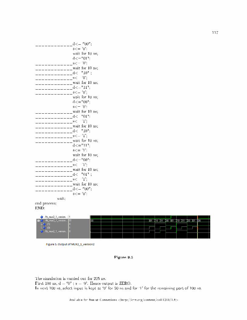
117
____________d<= "00";____________s<= '0';____________wait for 10 ns;____________d<="01";____________s<= '0';____________wait for 10 ns;____________d<="10" ;____________s<= '0';____________wait for 10 ns;____________d<="11";____________s<= '0';____________wait for 10 ns;____________d<="00";____________s<= '0';____________wait for 10 ns;____________d<="01";____________s<= '1';____________wait for 10 ns;____________d<="10";____________s<= '1';____________wait for 10 ns;____________d<="11";____________s<= '1';____________wait for 10 ns;____________d<="00";____________s<= '1';____________wait for 10 ns;____________d<="01" ;____________s<= '1';____________wait for 10 ns;____________d<= "00";____________s<= '0';_______wait;end process;END;
Figure 9.5
The simulation is carried out for 225 ns.First 100 ns, d = �0� ; s = `0'. Hence output is ZERO.In next 100 ns, select input is kept at `0' for 50 ns and for `1' for the remaining part of 100 ns.
Available for free at Connexions <http://cnx.org/content/col11213/1.8>

118CHAPTER 9. DSD_CHAPTER 4_VHDL APPLICATION TO SEQUENTIAL
CIRCUIT SYNTHESIS_PART2
When s = `0', y = d(0) which carries a periodic waveform of Period 20 ns. Hence for this 50 ns, y carriesa periodic waveform of Period 20 ns.
When s = `1', y = d(1) which carries a periodic waveform of Period 40 ns. Hence for the remaining 50ns, y carries a periodic waveform of Period 40 ns.
This is called Time Divison Multiplexing (TDM) which is used in Digital Communication for passingmillion telephonic conversations on a single optical �ber.
For remaining 25 ns, d = �00�; s = `0'. Hence output is ZERO.MUX4_1LIBRARY ieee;USE ieee.std_logic_1164.ALL;USE ieee.std_logic_unsigned.All;USE ieee.numeric_std.ALL;ENTITY Tb_mux4_1 ISEND Tb_mux4_1;ARCHITECTURE behavior OF Tb_mux4_1 IS� Component Declaration for the Unit Under Test (UUT)COMPONENT mux4_1PORT(___s : IN std_logic_vector(1 downto 0);___d : IN std_logic_vector(3 downto 0);___y : OUT std_logic____);END COMPONENT;�Inputssignal s : std_logic_vector(1 downto 0) := (others => '0');signal d : std_logic_vector(3 downto 0) := (others => '0');�Outputssignal y : std_logic;BEGIN� Instantiate the Unit Under Test (UUT)uut: mux4_1 PORT MAP (____s => s,____d => d,____y => y_____);� No clocks detected in port list. Replace <clock> below with� appropriate port name� constant <clock>_period := 100 ns;�� <clock>_process :process� begin� <clock> <= '0';� wait for <clock>_period/2;� <clock> <= '1';� wait for <clock>_period/2;� end process;� Stimulus processstim_proc: processbegin� hold reset state for 100 ns.wait for 100 ns;
Available for free at Connexions <http://cnx.org/content/col11213/1.8>

119
� insert stimulus here____________d<= "0101";____________s<= "00";____________wait for 50 ns;____________s<= "01";____________wait for 50 ns;____________s<= "10";____________wait for 50 ns;____________s<= "11";____________wait for 50 ns;____________d<= "0000";____________s<= "00";___________wait;end process;END;
Figure 9.6
______Upper Trace is s: std_logic_vector(1 downto 0);____________Next subtrace is s(1) which is `0' for 50ns, `1' for 100ns, `0' for the remaining time;____________Next subtrace is s(0) which alternates between `0' a nd `1' for 200ns;_______Lower Trace is d: std_logic_vector(3 downto 0);____________This vector d is kept at �0101�for 200ns;_______Lowest Trace is y: y samples d(0) for 50ns, d(1) for 50ns, d(2) for 50ns and d(3) for last
50ns of the 200ns active time.
Available for free at Connexions <http://cnx.org/content/col11213/1.8>

120CHAPTER 9. DSD_CHAPTER 4_VHDL APPLICATION TO SEQUENTIAL
CIRCUIT SYNTHESIS_PART2
Available for free at Connexions <http://cnx.org/content/col11213/1.8>

Chapter 10
Chapter 5_ DSD_Moore and Mealy
State Machines.1
Chapter 5_ DSD_Moore and Mealy State Machines.5.1. Why do we construct State Machines ?In 1942, Manhatten Project was launched by US Government in Los Alamos National Laboratory in
absolute secrecy. J. Robert Oppenheimer, the renowned nuclear scientist from University of CaliforniaBerkeley, was heading this Project. The aim of this Project was to develop the nuclear �ssion bomb morecommonly known as Atom Bomb. [Two atom bombs named `Little Boy' and `Fat Man' were subsequentlydropped on Hiroshima and Naqasaki, Japan, respectively on 6th August 1945 and this catastrophe forcedJapan to surrender bringing an end to World War II ]
In course of this development huge amount of theoretical calculations were required for which StoredProgram Digital Computers were required. The concept of stored program digital computer was �rst pro-posed by Allan Turing in 1936. Inspired by the lectures of Max Newman at the University of Cambridgeon Mathematical Logic, Allan Turing wrote a paper on On Computable Numbers, with an Application tothe Entscheidungsproblem, which was published in the Proceedings of the London Mathematical Society.This gave birth to Universal Turing Machine. Huge amount of Data Crunching requirement in Manhat-ten Project necessitated the development of Stored Program Computer called EDVAC(Electronic DiscreteVariable Automatic Computer).
John von Neumann became involved with Manhatten Project for the sake of development of StoredProgram Digital Computer. Von Neumann was a Hungarian American Mathematician who was consideredto be the last of the great mathematicians and who subsequently won the title of Father of Modern DigitalComputer. He submitted First Draft of a Report on the EDVAC2 dated 30 June 1945. This was inspired byUniversal Turing Machine and this was known as von Neumann Architecture. Stored-program computerswere an advancement over the program-controlled computers of the 1940s, such as the Colossus3 and theENIAC4 , which were programmed by setting switches and inserting patch leads to route data and to controlsignals between various functional units. ENIAC used to take 3 weeks to write a new program and get itrun.
1This content is available online at <http://cnx.org/content/m35681/1.1/>.2http://en.wikipedia.org/wiki/First_Draft_of_a_Report_on_the_EDVAC3http://en.wikipedia.org/wiki/Colossus_computer4http://en.wikipedia.org/wiki/ENIAC
Available for free at Connexions <http://cnx.org/content/col11213/1.8>
121

122 CHAPTER 10. CHAPTER 5_ DSD_MOORE AND MEALY STATEMACHINES.
Figure 10.1
Figure 1. Schematic of von Neumann Architecture of Stored Program Digital Computer.In Figure 1, the proposed architecture is shown. In this new architecture , Memory and
CPU(ALU+Control Unit) are separated. Memory stores both data and instructions. This works sequen-tialy. Through Data Buses the data is sent to and fro between the memory and CPU. CPU works muchfaster than the availability of data. This is because CPU processing speed is being scaled up with each newgeneration of technology but the rise in bus speed is not commensurate. Hence we face a limited throughputbetween memory and CPU as compared to the size of the memory. Because of the limited throughput CPUis continuously waiting for data after completing its number crunching. This considerably slows down theInstructions per second execution. This slowing down of computer is due to �von Neumann Bottleneck�and it can be removed by matching the bus speed with CPU processing speed. Several methods have beensuggested to overcome this problem.
In the initial phase three standard methods were suggested to overcome von Neumann bottle neck:
i. A cache memory between the main memory and CPU. This cache memory stores the current data andmakes it readily available to CPU. For rapid exchange of Data between cache and CPU, cache is madeof SRAM whereas the main memory is DRAM. SRAM is made of BJT and has a much faster accesstime as compared to that of DRAM which is made of CMOS.
ii. Providing separate Caches and separate access paths for data and instructions. This is known asHarvard Architecture.
iii. Using Branch predictor and logic.
Recently in contrast to sequential Architecture/von Neumann Architecture/Scalar Architecture, parallelarchitecture/vector architecture has been introduced to overcome the problem of von Neumann architecture.
The notable vector architectures are:
a. Systolic Architecture.b. Data-�ow Architecture.c. Pipeline Architecture.
Available for free at Connexions <http://cnx.org/content/col11213/1.8>

123
This has eased the bottleneck but not eradicated the problem. Construction of `State Machines' is a step inthat direction. Here it may be mentioned in passing that all these architectures are based on `AlgorithmicProgramming' which use `Boolean Logic'. This is in contrast to `Heuristic Programming' which is basedon `Rules of Thumb' and which uses `Predicate Logic'. The Fifth Generation Computers more commonlyknown as Arti�cial Intelligence Machines are based on heuristic programming and use `LISP' and `PROLOG'programming languages. These have already come in the market and are being used as Knowledge ExpertSystems in Health, Care and Delivery.
To appreciate the superiority of State Machines over the present Desk Top Computers we must look atthe following VHDL example which can be run on both State Machine and CPU:
If a > 37 and c < 7 then___State <= alarm;___Out_a <= `0';___Out_b <= `0';___Out_analog <= a+b;Else___State <= running;End if;This program de�nes two states: `ALARM' state and `RUN' state. When condition 1 namely `a > 37
and c < 7' is ful�lled the machine is put in Alarm state and if condition 2 namely `a < 37 and c > 7' isful�lled then machine is put in Run state.
If this program is implemented on CPU, the program will be translated into 10 to 20 machine instructionstaking more than 10 to 20 clock cycles time to execute the program. But if the same program is implementedin gates and �ip-�ops as it is done in State Machine then the whole program will be executed in one clockcycle. Hence State Machines implemented in logic gates and �ip-�ops is much more powerful than CPU.
5.2. State Machine Architecture.The block diagram of a State Machine is given in Figure 2 below.
Available for free at Connexions <http://cnx.org/content/col11213/1.8>

124 CHAPTER 10. CHAPTER 5_ DSD_MOORE AND MEALY STATEMACHINES.
Figure 10.2
Figure 2. Block Diagram of State Machine.As seen in Figure 2, Register has the code of a given state. This code is applied to the Logic Network.
In accordance with the current state code, Logic Network responds. It takes some time to respond to theapplied state code. Once Logic Network has settled to the new state as dictated by the state code applied toit, it de�nes and applies a new state code to the Register. At the next clock pulse this new code is writtenand stored in the register. This is called sampling. Register samples the new state code. In between the clockpulses, a new state code is applied to Logic Network. In this way through a series of clocks pulses, LogicMachine moves through all the states de�ned by the program and accomplishes it tasks. This is achieved ina much shorter time. As can be seen in the state diagram, the logic machine should have settled to a stablestate before a clock pulse is applied and before the new state code is sampled into the register. Thus a StateMachine is a clocked sequential circuit and it goes through �nite number of states hence it is called FiniteState Machines (FSM).
5.3. Two kinds of State Machines: Mealy and Moore Machine.There are two kinds of State Machines:
i. Mealy Machine is a function of the current state code as well as the current inputs.ii. Moore Machine is a function of the current state code only.
Available for free at Connexions <http://cnx.org/content/col11213/1.8>

125
Figure 10.3
Mealy Machine:
• In a Mealy Machine, the outputs are a function of the present state and the value of the current inputsas shown in Figure 3.
• Accordingly the outputs of a Mealy Machine can change asynchronously in response to any change inthe inputs. The output need not change at a Clock Pulse.
Available for free at Connexions <http://cnx.org/content/col11213/1.8>
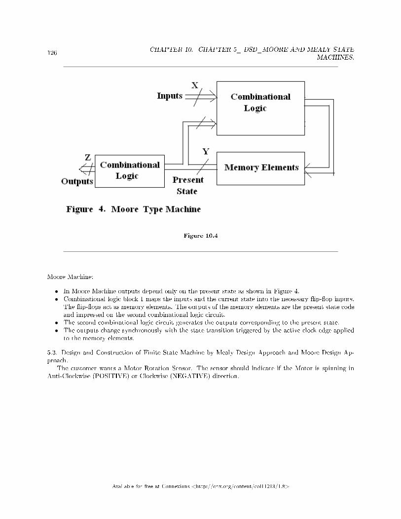
126 CHAPTER 10. CHAPTER 5_ DSD_MOORE AND MEALY STATEMACHINES.
Figure 10.4
Moore Machine:
• In Moore Machine outputs depend only on the present state as shown in Figure 4.• Combinational logic block 1 maps the inputs and the current state into the necessary �ip-�op inputs.
The �ip-�ops act as memory elements. The outputs of the memory elements are the present state codeand impressed on the second combinational logic circuit.
• The second combinational logic circuit generates the outputs corresponding to the present state.• The outputs change synchronously with the state transition triggered by the active clock edge applied
to the memory elements.
5.3. Design and Construction of Finite State Machine by Mealy Design Approach and Moore Design Ap-proach.
The customer wants a Motor Rotation Sensor. The sensor should indicate if the Motor is spinning inAnti-Clockwise (POSITIVE) or Clockwise (NEGATIVE) direction.
Available for free at Connexions <http://cnx.org/content/col11213/1.8>

127
Figure 10.5
Figure 5. Schematic Diagram of the Architecture of Rotation Sensing Machine.As can seen from Figure 5 there are two Sensors 1 and 2 which are so spatially placed that they generate
a square wave with 90 degree phase shift corresponding to P1 and P2. When both are `00' then NegativeRotation changes this to `01' and Positive Rotation changes this to `10'.
We will consider this problem later in this chapter.5.4. Comparison of Mealy and Moore Machines while designing `10' pattern detector.
Available for free at Connexions <http://cnx.org/content/col11213/1.8>

128 CHAPTER 10. CHAPTER 5_ DSD_MOORE AND MEALY STATEMACHINES.
Figure 10.6
Figure 6. The state diagrams of Mealy and Moore Machines designed for detecting `10' pattern.Problem 1 : Our customer has asked for `10' Sequence Detector . This should give an output HIGH only
when `10' sequence is detected.We will design a FSM(Finite State Machine) which checks for `10' pattern and when such a pattern is
detected it gives an output HIGH otherwise output is maintained LOW.We can take both Mealy Machine approach as well as Moore Machine approach.First let us consider Mealy Machine State Diagram given on the left of Figure 6.Mealy Machine State Diagram lists the input/associated_output on the state transition arcs.There are two distinct states: `initial'state and `1' state.
• When input is 0 , machine remains in `initial' state.• When input is 1 , output is LOW and machine makes a transition to state `1'.• If input is again `1', the pattern is `11' and output remains LOW and machine continues in state `1'.• But if instead of `1' the second input is `0' then we have obtained the desired pattern `10'. Hence
output goes HIGH and machine is RESET therefore it reverts to `initial state'.
Let us consider Moore Machine State Diagram given on right hand side of Figure 6.A Moore Machine produces an unique output for every state irrespective of inputs.
Available for free at Connexions <http://cnx.org/content/col11213/1.8>

129
Accordingly the state diagram of the Moore Machine associates the output with its respective state inthe form state-notation/output-value.
State transition arrows of Moore Machine are labeled with the input value that triggers the transition.As seen in the state diagram Figure 6, there are three distinct states: `initial' , `1' and `11'.
• In the state `initial', output is LOW. If the �rst input is 0 , machine remains in `initial' state.• If the �rst input is 1 then this input triggers the transition to the second state `1' and since the desired
pattern is not achieved therefore output remains LOW but we have moved one step in the direction ofdesired detection.
• If the second input is 1, we remain in state `1' and output remains LOW. We continue to remain instate `1' because we can hope to detect `10' pattern at the third input.
• But if second input is 0, we have hit the Jack Pot. Hence we move to the third state `10' whichcorresponds to output HIGH.
• If the third input is 1, we revert to state `1' because at fourth input = 0 we can again hit the Jack Pot.• But if the third input is 0 at the fourth input we can never hit the Jack Pot hence we reset to `initial
`state.
Problem 2 : My customer has asked for `111' Sequence Detector . This should give an output HIGH onlywhen `111' sequence is detected.
Solution 2.1. Design of Mealy Machine as `111'sequence detector.
Figure 10.7
Figure 7. The state diagrams of Mealy Machine designed for detecting `111' pattern.In Figure 7 we describe the state diagram of a Mealy Machine which will be a `111' sequence detector.This Finite State Machine has three distinct states: Initial State, Got-1 state and Got-11 state.
• Initial state should clearly be a reset state where input is 1 and output is 1.
Available for free at Connexions <http://cnx.org/content/col11213/1.8>

130 CHAPTER 10. CHAPTER 5_ DSD_MOORE AND MEALY STATEMACHINES.
• When �rst input is 0, machine remains in initial state with output LOW.• When �rst input is 1, output remains LOW but FSM makes a transition to Got-1 state. The machine
is one step nearer the Jackpot.• When second input is 0, output remains LOW and machine reverts back to Initial State.• When second input is 1, output remains LOW but now it is two steps nearer the Jackpot hence FSM
makes a transition to Got-11 state.• When third input is 0, output remains LOW and the FSM resets as there is no chance of hitting the
Jackpot at the fourth input.• But when third input is 1, the Jackpot is hit and output is HIGH but FSM remains at Got-11 state
because at the fourth input , if 1, it can again hit the Jackpot.
In Figure 8, we do the circuit implementation of `111' sequence detector.
Figure 10.8
Figure 8. Mealy State Machine for `111' sequence detection Circuit Implementation.The TIMING DIAGRAM for the circuit in Figure 8 is given in Figure 9.
Available for free at Connexions <http://cnx.org/content/col11213/1.8>

131
Figure 10.9
Figure 9. Timing Diagram for `111' Sequence Detector.Let us examine the operation of Mealy Machine as `111' detector.Initially A and B are in reset condition. Hence Qa and Qb are LOW and Qa* and Qb* (the complements)
are HIGH. Initially X= 0. So initial condition is de�ned as X=0, Da=0,Db=0Qa=0 , Qb =0 and Z=0. Thisis `initial state AB=00'.
Next suppose X =1. This is second state `Got-1_AB=01'.As seen from Figure 9, Db = X.Qa*.Qb* and Da = X.Qa + X.Qb.And Z = X.QaHence �rst input HIGH makes Db HIGH but Da remains LOW. Therefore in second state we have AB=01
and Z=0.Suppose the second input is also X = 1.Now as soon as Clock appears, at the lagging edge of the Clock(since Clock has a bubble) Db=1 is entered
into Db Flip Flop. Hence Qb =1 and Qb* =0.So Da = 1 and Db = 0.At the next clock A_FF is set and B_FF is reset. Therefore Third state is `Got-11_AB=10'. And if X
continues to be HIGH then Z= 1.Thus a string `111' is detected and output is HIGH.Table 1. State Transition Table of Mealy Machine as `111' string detector.
Available for free at Connexions <http://cnx.org/content/col11213/1.8>

132 CHAPTER 10. CHAPTER 5_ DSD_MOORE AND MEALY STATEMACHINES.
State X Da Db Qa|N Qa|N+1 Qb|N Qb|N+1 Z|NInitial 0 0 0 0 0 0 0 0
Got-1_AB=01 1 0 1 0 0 0 1 0
Got-11_AB=10 1 1 0 0 1 1 0 0
Got-11_AB=10 1 1 0 1 1 0 0 1
Table 10.1
As can be seen in Figure 9 , X remains HIGH for some time when A_FF is SET and B_FF is RESETat the third Lagging Edge of the Clock. This gives a `FALSE HIGH' known as `OUTPUT GLITCH'.
Solution 2.2. Design of Moore Machine as `111' sequence detector.
Available for free at Connexions <http://cnx.org/content/col11213/1.8>

133
Figure 10.10
Figure 10. Four distinct States of Moore Machine for detecting a string of `111'.As seen in Figure 10 there are four distinct states:
• First is the initial state/output =0 when the system is in RESET condition.• Second is `1'/0, when a string `1' is detected and output is LOW.• Third is `11'/0 when a string `11' is detected and output is still LOW.• Fourth is `111'/1 when a string `111' is detected and output is HIGH. We have hit the Jackpot.• We have shown how it reverts back to a former state when 0 is inputted. This happens four times as
shown by arcs.
Figure 10 state diagram is converted into equivalent State Table in Table 2.
Available for free at Connexions <http://cnx.org/content/col11213/1.8>

134 CHAPTER 10. CHAPTER 5_ DSD_MOORE AND MEALY STATEMACHINES.
Table 2. State Table of Moore Machine as detector of `111'sequence.
State description output
Initial Initial/0 0
Got-1 `1'/0 0
Got-11 `11'/0 0
Got-111 `111'/1 1
Table 10.2
Table 3.State Transition Table and Output Table.
Present State Next State Output
X = 0 X = 1 Z
Initial Initial Got-1 0
Got-1 Initial Got-11 0
Got-11 Initial Got-111 0
Got-111 Initial Got-111 1
Table 10.3
We will use J-K FF and D-FF for the implementation Moore Machine as `111' string detector. Table 4and Table 5 give the excitation table for J-K_FF and D_FF.
Table 4. Excitation Table of J-K_FF[Q(N) is the output before the clock and Q(N+1) is the output after the clock]
J K Q(n) Q(n+1) Comment
0 × 0 0 When J =0then K=0 givesNOCHANGE con-dition and K=1gives RESET.Hence O/P is 0 ifQ(N)=0;
continued on next page
Available for free at Connexions <http://cnx.org/content/col11213/1.8>

135
1 × 0 1 When J =1 thenK=1 gives TOG-GLE conditionand K=0 givesSET. Hence O/Pin either case is 1if Q(N)=0;
× 1 1 0 When K=1 thenJ=1 gives TOG-GLE and J=0gives RESET.Hence O/P is 0in either case ifQ(N)=1;
× 0 1 1 When K=0 thenJ=1 gives SETand J=0 givesNOCHANGE.Hence O/P is 1in either case ifQ(N)=1;
Table 10.4
Table 5. Excitation Table of D_FF
D Q(n) Q(n+1)
0 0 0
1 0 1
0 1 0
1 1 1
Table 10.5
These excitation tables have been derived from Truth-Table of J-K_FF and D_FF.Table 6. Combined Truth Table of J-K_FF and D_FF.
J K Q(N+1) D Q(N+1)
No change 0 0 Q(N) 0 0
RESET 0 1 0 1 1
SET 1 0 1
TOGGLE 1 1 Q(N)*
Table 10.6
Table 7. Excitation Table for the Moore implementation.
Available for free at Connexions <http://cnx.org/content/col11213/1.8>

136 CHAPTER 10. CHAPTER 5_ DSD_MOORE AND MEALY STATEMACHINES.
Present State Input Next State FF_Inputs Output
A B X A B Ja Ka Db Z
0 0 0 0 0 0 × 0 0
0 0 1 0 1 0 × 1 0
0 1 0 0 0 0 × 0 0
0 1 1 1 0 1 × 0 0
1 0 0 0 0 × 1 0 0
1 0 1 1 1 × 0 1 0
1 1 0 0 0 × 1 0 1
1 1 1 1 1 × 0 1 1
Table 10.7
Simplifying Table 7 using Karnaugh's Map we get the following Logic Functions.
• Ja = X.B• Ka = X*• Db = X(A+B)• Z = A.B
The output is a function of current state only.
Available for free at Connexions <http://cnx.org/content/col11213/1.8>

137
Figure 10.11
Figure 11. A Moore Machine Logic Circuit and FF con�guration for `111' sequence detector.The Timing Diagram for Moore Machine is shown in Figure 12. There is no output glitch in Moore
Model. This is because the output depends on clearly de�ned states of the Flip-Flop which are synchronizedwith clock. The outputs remain valid through out the logic state.
Available for free at Connexions <http://cnx.org/content/col11213/1.8>

138 CHAPTER 10. CHAPTER 5_ DSD_MOORE AND MEALY STATEMACHINES.
Figure 10.12
Figure 12. Timing Diagram for Moore Model of string detector.State Machine implementation of string detector of any size `11' or `111' involves much less clock cycles
as compared to the same string detector implemented on CPU of a Personal Computer.
Available for free at Connexions <http://cnx.org/content/col11213/1.8>
Chapter 11
DSD_Chapter 5_StateMa-
chines_Part3_MooreMachine Motor
Rotation Sensor Design and Synthesis.1
DSD_Chapter 5_StateMachines_Part2_MooreMachineDesign5.5 Designing and implementing Motor Rotation Sensor.The customer wants a Motor Rotation Sensor. The sensor should indicate if the Motor is spinning in
Anti-Clockwise (Negative) or Clockwise (Positive) direction.
1This content is available online at <http://cnx.org/content/m46067/1.1/>.
Available for free at Connexions <http://cnx.org/content/col11213/1.8>
139

140CHAPTER 11. DSD_CHAPTER
5_STATEMACHINES_PART3_MOOREMACHINE MOTOR ROTATIONSENSOR DESIGN AND SYNTHESIS.
Figure 11.1
Figure 1.Schematic Diagram of the Architecture of Rotation Sensing Machine.As can seen from Figure 1 there are two Sensors 1 and 2 which are so spatially placed that they generate
a square wave with 90 degree phase shift corresponding to P1 and P2. When both are `00' then NegativeRotation changes this to `01' and Positive Rotation changes this to `10'.
We will take Moore Machine Design approach. Figure 2 gives the state diagram:
Available for free at Connexions <http://cnx.org/content/col11213/1.8>

141
Figure 11.2
Figure 2. State Diagrams ofRotation Sensing Machine.As shown in Figure 3 , the state code is sampled and stored in the REGISTER at the lagging/leading
edge of the clock pulse. The state code in the Register decides the output. Since there are four distinctSTATES hence there are four distinct OUTPUTS. So we have two-bit CODE {a0 , a1} to de�ne the fourstates and we have two-bit std_logic_vector output �b0b1� to de�ne the four corresponding outputs.
The two-bit std_logic_vector input �P1P2� are obtained from the sensors mounted over the encodingdisc which in turn is mounted on the axle of the rotating motor. The Clock of the REGISTER must besynchronized with the motor speed so that all the four states are continuously monitored by the REGISTER.
If S2 state follows S1 then we have LED1 lit up which signi�es that negative rotation of the motor andif S3 follows S1 then LED2 lights up signifying positive rotation.
Available for free at Connexions <http://cnx.org/content/col11213/1.8>
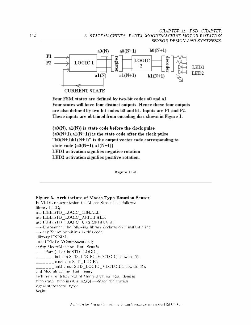
142CHAPTER 11. DSD_CHAPTER
5_STATEMACHINES_PART3_MOOREMACHINE MOTOR ROTATIONSENSOR DESIGN AND SYNTHESIS.
Figure 11.3
Figure 3. Architecture of Moore Type Rotation Sensor.In VHDL representation the Moore Sensor is as follows:library IEEE;use IEEE.STD_LOGIC_1164.ALL;use IEEE.STD_LOGIC_ARITH.ALL;use IEEE.STD_LOGIC_UNSIGNED.ALL;�- Uncomment the following library declaration if instantiating�- any Xilinx primitives in this code.�library UNISIM;�use UNISIM.VComponents.all;entity MooreMachine_Rot_Sens is___Port ( clk : in STD_LOGIC;______in1 : in STD_LOGIC_VECTOR(1 downto 0);______reset : in STD_LOGIC;______out1 : out STD_LOGIC_VECTOR(1 downto 0));end MooreMachine_Rot_Sens;architecture Behavioral of MooreMachine_Rot_Sens istype state_type is (s0,s1,s2,s3);�-State declarationsignal state:state_type;begin
Available for free at Connexions <http://cnx.org/content/col11213/1.8>
143
process(clk,reset)�clocked processbegin______if reset= '1' then____________state<= s0;���reset state______elsif clk'event and clk= '1' then____________case state is____________when s0=>__________________if in1 = "00" then_______________________state<=s1;_________________end if;____________when s1=>__________________if in1 = "10" then________________________state<=s2;__________________elsif in1 = "01" then________________________state<=s3;__________________elsif in1 = "11" then________________________state<=s0;__________________end if;____________when others=> null;____________end case;______end if;end process;output_p:process(state) �- combinational processbegincase state iswhen s0=> out1<= "00";when s1=> out1<= "01";when s2=> out1<= "10";when s3=> out1<= "11";when others=> null;end case;end process;end Behavioral;This is the complete VHDL description of MooreMachine_Rot_Sens.By clicking Synthesis XST we do Syntax Check.After we have made VHDL codes SYNTAX ERROR free, we click LEFT HAND CORNER of Synthesis
-XST. We get the following.
Available for free at Connexions <http://cnx.org/content/col11213/1.8>

144CHAPTER 11. DSD_CHAPTER
5_STATEMACHINES_PART3_MOOREMACHINE MOTOR ROTATIONSENSOR DESIGN AND SYNTHESIS.
Figure 11.4
On clicking �View Synthesis Report� we get the following:TABLE OF CONTENTS1) Synthesis Options Summary2) HDL Compilation3) Design Hierarchy Analysis4) HDL Analysis5) HDL Synthesis5.1) HDL Synthesis Report6) Advanced HDL Synthesis6.1) Advanced HDL Synthesis Report7) Low Level Synthesis8) Partition Report9) Final Report9.1) Device utilization summary9.2) Partition Resource Summary9.3) TIMING REPORTWhile doing the actual simulation, we can see the detailed Synthesis Report.On clicking �View RTL Schematic� we can see the register level description of the Moore Machine. It is
as follows:
Available for free at Connexions <http://cnx.org/content/col11213/1.8>

145
Figure 11.5
Figure 4. Register Level Description of the Moore Machine.
Figure 11.6
Figure 5.Enlarged version of Register Level Description of the Moore Machine.By clicking the RTL schematic we get the enlarged version as shown in Figure 5.
Available for free at Connexions <http://cnx.org/content/col11213/1.8>

146CHAPTER 11. DSD_CHAPTER
5_STATEMACHINES_PART3_MOOREMACHINE MOTOR ROTATIONSENSOR DESIGN AND SYNTHESIS.
By clicking the �View Technology Schematic� we get RTL schematic as in Figure 4. By clicking RTLschematic we get the Technology Schematic as shown in Figure 6. In Figure 6, we have LUT(Look Up Table)and FDC(Floppy Disk Controller). FDC is D Flip Flop with asynchronous CLEAR and Data Output.
Next we have Syntax Check. We have already done it and made our program syntax error free.Next we have �Generate Post Synthesis Simulation Model�. This is for higher level synthesis. We will
not deal with it here.
Figure 11.7
Figure 6. Technology Schematic of the Moore Sensor.Next we click at the left hand corner of �Implement Design�.As seen above we get `Translate', `Map' and `Place and Rout'.By clicking `Translate', we translate VHDL codes in FPGA readable programs.By clicking `Map', my VHDL design is mapped on FPGA Archtecture.By clicking `Place & Rout', my VHDL hardware is placed on FPGA platform.Next we click at the left hand corner of �Generate Progamming File�. We get a sub-title `Programming
File Generation Report'. By clicking this sub-title we get BIT �le of my VHDL program.Next we have �Con�gure Target Device�. Through programmable cable (parallel or USB). BIT �le of my
VHDL program is downloaded on the FPGA kit.Now we create the Test Bench of MooreMachine_Rot_Sens.� This testbench has been automatically generated using types std_logic and� std_logic_vector for the ports of the unit under test. Xilinx recommends� that these types always be used for the top-level I/O of a design in order� to guarantee that the testbench will bind correctly to the post-implementation� simulation model.���������������������������LIBRARY ieee;USE ieee.std_logic_1164.ALL;USE ieee.std_logic_unsigned.all;USE ieee.numeric_std.ALL;ENTITY mooremachineTB ISEND mooremachineTB;ARCHITECTURE behavior OF mooremachineTB IS� Component Declaration for the Unit Under Test (UUT)
Available for free at Connexions <http://cnx.org/content/col11213/1.8>

147
COMPONENT mooremachinerotation_sensorPORT(clk : IN std_logic;in1 : IN std_logic_vector(1 downto 0);reset : IN std_logic;out1 : OUT std_logic_vector(1 downto 0));END COMPONENT;�Inputssignal clk : std_logic := '0';signal in1 : std_logic_vector(1 downto 0) := (others => '0');signal reset : std_logic := '0';�Outputssignal out1 : std_logic_vector(1 downto 0);� Clock period de�nitionsconstant clk_period : time := 20 ns;BEGIN� Instantiate the Unit Under Test (UUT)uut: mooremachinerotation_sensor PORT MAP (clk => clk,in1 => in1,reset => reset,out1 => out1);� Clock process de�nitionsclk_process :processbegin____________clk <= '0';____________wait for clk_period/2;____________clk <= '1';____________wait for clk_period/2;end process;� Stimulus processstim_proc: processbeginwait for 20ns;reset<= '0';wait for 20ns;in1<= "00";wait for 100ns;in1<= "01";wait for 100ns;reset<= '1';wait for 20ns;reset<= '0';wait for 20ns;in1<= "00";wait for 100ns;in1<= "10";wait for 100ns;reset<= '1';
Available for free at Connexions <http://cnx.org/content/col11213/1.8>

148CHAPTER 11. DSD_CHAPTER
5_STATEMACHINES_PART3_MOOREMACHINE MOTOR ROTATIONSENSOR DESIGN AND SYNTHESIS.
wait for 20ns;� insert stimulus herewait;end process;END;The ModelSim output is the following:
Figure 11.8
Figure 7. Output of MooreMachine_Rotation Sensor.As can be seen from ModelSim traces, at �00�input, the Moore Machine transits to S1/�01� at the next
leading edge of the clock pulse.�00� is followed �01� and the machine transit to S3/�11� at the leading edge of the Clk Pulse. This is
decoded as Positive Rotation.Asynchronous input RESET is enabled by giving `1'. Immediately Machine transits to S0/�00� without
any delay.Asynvhronous input doesnot require Clk Pulse.In the diagram we see the �rst Reset='1' for 20ns. This appears as a narrow pulse.After RESETTING we disable RESET input by making reset='0'.Now �00� is followed by �10� the output is S2/�10� at the leading edge of the Clk Pulse. This is decoded
as Negative Rotation.By enabling the RESET the second time , we again RESET the Machine to S0/�00�stste.
Available for free at Connexions <http://cnx.org/content/col11213/1.8>

Chapter 12
DSD_Chapter 5_Part 3_Design of a
Mealy Machine_Rotation_Sensor1
DSD_Chapter 5_Part 3_Design of a Mealy Machine.Moore Machine's output depends only on the state code whereas Mealy Machine's output depends on
the inputs + the current state code.5.6 Designing and implementing Motor Rotation Sensor using Mealy Machine Design ap-
proach.We will restate the problem here. Refer to Figure 1 of Chapter 5_Part 2. Input is a standard logic vector
of 2-bit length. It can be �00� , �01� , �10� , �11� .If �00� is followed by �01� it denotes positive rotation.If �00� is followed by �10� it denotes negative rotation.In Moore Machine we have the following State Transition Table.Table 1. State Transition Table of Mealy Machine.
Reset In1 State Out1
1 �Φ1Φ2� S0 �00� No output
0 �00� S0→S1 �01� No output.
0 00→�10� S1→S2 �10� LED denoting NEGATIVE ROTATION will light up
0 00→�01� S1→S3 �11� LED denoting POSITIVE ROTATIN will light up
0 00→�11� S1→S0 �00� No output
Table 12.1
�00� triggers the transition from S0→S1 at Clk'event.�10� triggers the transition from S1→S2 at Clk'event.�01� triggers the transition from S1→S3 at Clk'event.�11� triggers the transition from S1→S0 at Clk'event.
1This content is available online at <http://cnx.org/content/m35737/1.2/>.
Available for free at Connexions <http://cnx.org/content/col11213/1.8>
149

150CHAPTER 12. DSD_CHAPTER 5_PART 3_DESIGN OF A MEALY
MACHINE_ROTATION_SENSOR
Figure 12.1
Through Process P0, current state + IN1 generate the next state. Simultaneously current state throughProcess P2 generates its unique OUT1.
In Moore Machine, OUT1=Function(Current State).At Clk'event, the next state is entered into the REGISTER and is made available for `n+1' event.When RESET is activated then Register always initializes to S0. Then RESET must be disabled.Only after disabling RESET, the system will respond to the Clk'event.We can implement the same requirement through Mealy Machine.In Mealy Machine, OUT1 = Function(IN1,Current State).So there is a di�erent architecture also as shown in Figure 2.
Available for free at Connexions <http://cnx.org/content/col11213/1.8>

151
Figure 12.2
If we compare the two architectures, Mealy Machine is de�nitely simpler to implement with less hardware.State Transition Table of Mealy Machine.Table 2. State Transition Table.
Reset In1 State Out1
1 `Φ1Φ2' S0 �00� No output
0 `00' S0→S1 �01� No output.
0 `00'→ `10' S1→S2 �10� LED denoting NEGATIVE ROTATION will light up
0 `00'→ `01' S1→S3 �11� LED denoting POSITIVE ROTATIN will light up
0 `00'→ `11' S1→S0 �00� No output
Table 12.2
�00� triggers the transition from S0→S1 at Clk'event.�10� triggers the transition from S1→S2 at Clk'event.�01� triggers the transition from S1→S3 at Clk'event.�11� triggers the transition from S1→S0 at Clk'event.State Transition Diagram of Mealy Machine.
Available for free at Connexions <http://cnx.org/content/col11213/1.8>

152CHAPTER 12. DSD_CHAPTER 5_PART 3_DESIGN OF A MEALY
MACHINE_ROTATION_SENSOR
Figure 12.3
Figure 3. State Transition Diagram of Motor Rotation Sensor based on Mealy MachineDesign.
The arcs contain the input which causes the transition between the respective states as shown.Now we will write the VHDL codes for Mealy Machine.library IEEE;use IEEE.STD_LOGIC_1164.ALL;use IEEE.STD_LOGIC_ARITH.ALL;use IEEE.STD_LOGIC_UNSIGNED.ALL;�- Uncomment the following library declaration if instantiating�- any Xilinx primitives in this code.�library UNISIM;�use UNISIM.VComponents.all;entity MealyMachine_Rot_Sens isPort ( clk : in STD_LOGIC;___ reset : in STD_LOGIC;___in1 : in STD_LOGIC_VECTOR(1 downto 0);___out1 : out STD_LOGIC_VECTOR(1 downto 0));end MealyMachine_Rot_Sens;architecture Behavioral of MealyMachine_Rot_Sens istype state_type is (s0,s1,s2,s3);
Available for free at Connexions <http://cnx.org/content/col11213/1.8>

153
signal state: state_type;beginprocess(clk,reset)begin_________if reset = '1' then____________state<=s0;____________elsif clk'event and clk= '1' then____________case state is__________________when s0=>______________________________if in1= "00" then______________________________state<=s1;______________________________end if;__________________when s1=>______________________________if in1 = "10" then______________________________state <= s2;______________________________elsif in1 = "01" then______________________________state <= s3;______________________________elsif in1 = "11" then______________________________state <= s0;______________________________end if;_________________when others => null;____________end case;end if;end process;output_p: process(state,in1) �- combinational processbegincase state iswhen s0 => if in1= "00" then______________________________out1 <= "01";______________________________else out1<= "00";______________________________end if;when s1=> if in1= "10" then______________________________out1 <= "10";______________________________elsif in1= "01" then______________________________out1 <= "11";_____________________________elsif in1="11" then_____________________________out1<= "00";_____________________________else out1<= "01" ;_____________________________end if;when s2=> if in1= "00" then______________________________out1 <= "01";______________________________else out1 <= "00";______________________________end if;when s3=> if in1= "00" then______________________________out1 <= "01";______________________________else out1 <= "00";______________________________end if;when others => null;end case;end process;end Behavioral;
Available for free at Connexions <http://cnx.org/content/col11213/1.8>

154CHAPTER 12. DSD_CHAPTER 5_PART 3_DESIGN OF A MEALY
MACHINE_ROTATION_SENSOR
We carry out Synthesize XST until we get syntax error free GREEN sign.Now we de�ne the TEST BENCH:LIBRARY ieee;USE ieee.std_logic_1164.ALL;USE ieee.std_logic_unsigned.all;USE ieee.numeric_std.ALL;ENTITY Tb_MealyMachine_Rot_Sens ISEND Tb_MealyMachine_Rot_Sens;ARCHITECTURE behavior OF Tb_MealyMachine_Rot_Sens IS� Component Declaration for the Unit Under Test (UUT)COMPONENT MealyMachine_Rot_SensPORT(clk : IN std_logic;reset : IN std_logic;in1 : IN std_logic_vector(1 downto 0);out1 : OUT std_logic_vector(1 downto 0));END COMPONENT;�Inputssignal clk : std_logic := '0';signal reset : std_logic := '1';signal in1 : std_logic_vector(1 downto 0) := (others => '0');�Outputssignal out1 : std_logic_vector(1 downto 0);� Clock period de�nitionsconstant clk_period : time := 20 ns;BEGIN� Instantiate the Unit Under Test (UUT)uut: MealyMachine_Rot_Sens PORT MAP (____clk => clk,____reset => reset,____in1 => in1,____out1 => out1);� Clock process de�nitionsclk_process :processbegin____________clk <= '0';____________wait for clk_period/2;____________clk <= '1';____________wait for clk_period/2;end process;� Stimulus processstim_proc: processbegin� hold reset state for 20 ns.____wait for 20 ns;� insert stimulus here____________reset<= '0';____________wait for 10 ns;____________in1<= "00";
Available for free at Connexions <http://cnx.org/content/col11213/1.8>

155
____________wait for 10 ns;____________in1<= "01";____________wait for 10 ns;____________in1<= "11";____________wait for 10 ns;____________in1<= "10";____________wait for 10 ns;____________in1<= "00";____________wait for 10 ns;____________in1<= "01";____________wait for 10 ns;____________in1<= "11";____________wait for 10 ns;____________in1<= "10";__wait;__end process;END;
Figure 12.4
First Line is Clock.Second Line is RESETThird Line is IN1____________sub third line MSB of IN1____________sub third line LSB of IN1Fourth Line is OUT1____________sub fourth line MSB of OUT1____________sub fourth line LSB of OUT1.Figure 4. Output of the ModelSim.We are having Positive Rotation hence out1 = �11� when in1 is �01� following �00�.
Available for free at Connexions <http://cnx.org/content/col11213/1.8>

156CHAPTER 12. DSD_CHAPTER 5_PART 3_DESIGN OF A MEALY
MACHINE_ROTATION_SENSOR
Available for free at Connexions <http://cnx.org/content/col11213/1.8>

Chapter 13
DSD_Chapter 5_Supplement_Optical
TERA BUS1
DSD_Chapter 5_ Supplement_Optical Fiber Inteconnects- A Novel Way of overcoming von-Neumann Bot-tlenecks.
[�Get on the Optical Bus�, IBM's light powered links overcome the greatest speed bump in supercom-puting: interconnect bandwidth, by Clint Schow, Fuad Doany and Je�rey Kash, September 2010, IEEESPECTRUM, pp 30-35]
As already discussed, in the classical von-Neumann Architecture there is a very serious bottleneck inthe availability of data for processing. The origin of this problem is the metallic interconnects which actas Data Bus as well as Instruction bus. As the Clock Speed go up, the problem is being compounded. Ingiga-Hz clock range, metallic interconnects face skin e�ect and eddy current losses. Skin e�ect leads toexcessive resistance of the conducting wires and consequent high heat dissipation. Also oscillating signalon the buses at very high frequency induces stray eddy current in the board's conducting part leading toheavy eddy current energy losses. With increase in Clock Rate, attenuation along the copper buses increasesexponentially. At 2 GHz clock there is 50% attenuation and at 10GHz there is 98% attenuation. At fewGHz several resonances occur which cause signal to be re�ected at VIAS. Vias are vertical conductors thatconnect two level components on Printed Circuit Board(PCB).
Apart from this there is severe cross-talk among the metallic interconnects leading to excessive bit-errorrate (BER). At 10 gigabits per second bit rates, cross talk blurs the signal after 1 meter of propogationdown the copper bus. With the increase in processing speed the problem of attenuation and cross-talk isbecoming more acute. Several methods were adopted to overcome the bandwidth bottleneck problem. Theforemost method amongst these is storing the current data in Cache Memory. Multigigahertz Clock ratehas been achieved within the microprocessor between processing core and on-chip cache memories but thedata exchange between the chip and external components ( say external memories) has been one order ofmagnitude slower.
This bandwidth gap between the processor and the buses will continue to widen as processor performanceimproves with scaling and improved processor architecture.
The problems of signal-loss and cross-talk is particularly severe in super-computers( massively parallelmachine) where we put together multi-chip modules together. Here the modules may be at two ends of thePCB or may be in di�erent racks of equipment.
Optical buses removes the problems of signal-loss, cross-talk problems and bandwidth bottleneck andmake the assembly of a supercomputer technically viable. Programming become simpler in supercomputersusing optically powered links because severe communication delays among processors donot have to becompensated while writing the programs.
1This content is available online at <http://cnx.org/content/m35738/1.1/>.
Available for free at Connexions <http://cnx.org/content/col11213/1.8>
157

158 CHAPTER 13. DSD_CHAPTER 5_SUPPLEMENT_OPTICAL TERA BUS
On 25th September 1956 TAT-1, transoceanic voice-grade coaxial cables were laid down and trans-Atlantictelephone calls became possible for the �rst time.
In 1988, TAT-8 optical �ber cables were laid across the bottom of Atlantic Ocean for trans-oceanicvoice-video-data cable transmission.
By 1990s, �ber-optic links were being used in local area networks (LANS) and in Storage Area Networks,interconnecting systems hundreds of meter apart. Optically linked LANS made Video-conferencing possiblewithin a campus.
In 2003 and 2004, fastest supercomputers were NEC Earth Simulator(5,120 processors running at a costof 17.5GFLOPS per million dollars) and IBM's Blue Gene L(65,536 processors with 10TFlOPS capabilityat a cost of 2.8TFLOPS per million dollars).Their peak performances reached 36 TFLOPS capability usingmetallic buses.
In 2008 IBM introduced RoadRunner using 40,000 optical �ber link buses. This reached Peta FLOPScapability. Peta means 1015. Hence Road runner had almost 2 orders of magnitude of performance improve-ment over that of Blue Gene L.
In IBM Blue Waters machine 1 million optical interconnects are being used. This is expected to reach10 PFLOPS capability. To achieve 1000-PFLOPS we will need 400 million optical links.
Judging from past performance we can say that Supercomputer processing rate will increase ten-foldevery four years.
Projected growth is shown in Table 1.Table 1. Growth in calculation capability of Suprcomputers.
Year Capability
2012 10PFlops
2016 100PFLOPS
2020 1000PFLOPS = 1ExaFLOPS(EFLOPS)
Table 13.1
TERA BUS Program was launched in 2003 as a collaborative program of IBM and Agilent.The architecture of TERA BUS is given in Figure 1.TERA BUS is essentially optical polymer waveguides interconnecting any number of modules of the
supercomputer. The module of the supercomputer contains an opto-chip which interfaces the electricalprocessor to optical TERA Bus. The back-side of the opto-chip receives
Available for free at Connexions <http://cnx.org/content/col11213/1.8>

159
Figure 13.1
Figure 1. Architecture of TERA BUS using optical �ber links.the optical signals from the optical BUS and launches the optical signals into the optical BUS. The opto-
chip is shown in Figure 1. At the front side of the opto-chip is CMOS Transceiver which receives electricalsignals from and transmits electrical signals to the Processor of the parallel machine.
In future we see that electrical connections will supply the power to the processor, it will provide theground and it will provide the control signals. Data will always move in and out of the processor as photonsand they will travel at the speed of light down the TERA BUS connecting the numerous processors.
Available for free at Connexions <http://cnx.org/content/col11213/1.8>

160 CHAPTER 13. DSD_CHAPTER 5_SUPPLEMENT_OPTICAL TERA BUS
Available for free at Connexions <http://cnx.org/content/col11213/1.8>

Chapter 14
DSD_Chapter 6_Mighty Spartans in
Action_Introduction.1
DSD_Chapter 6_Mighty Spartans in Action_Introduction.Spartan2 and Spartan3 is the name assigned to FPGA developed by the company Xilinx. This name
has come from the name Sparta of a City State in Greece in 1000BC. At that time there were two CityStates Sparta and Athens. Sparta had Oligarchy form of government whereas Athens had Democratic formof government.
Sparta was unique in the ancient times for its social system and constitution, which completely focusedon military training and excellence and it dominated Greece peninsula up to 300BC. Subsequently by 100BCit was conquered by Romans. Its inhabitants were classi�ed as Spartan citizens, who enjoyed full rights, non-Spartan free men raised as Spartans, freedmen and state-owned serfs (enslaved non-Spartan local population).Spartans underwent rigorous military training and education regimen, and Spartan soldiers were widelyconsidered to be among the best in battle. Spartan women enjoyed considerably more rights and equality tomen than elsewhere in the classical world. Spartans remained a city state which fascinated the people of allcultures and of all times. Thus we have FPGA named Spartan2 and Spartna3.
The following excerpts have been taken from EE Times:�Since their introduction in the mid-80s, FPGAs have managed to wedge themselves as a �xture into the
electronics design landscape. Sitting somewhere between o�-the-shelf (OTS) logic, ASICs, OTS processors,and ASSPs, they continue to enjoy growth predictions beyond those of the rest of the semiconductor industry�.
An application speci�c standard product or ASSP is an Integrated Circuit that implements aspeci�c function that appeals to a wide market. As opposed to ASIC that combines a collection of functionsand designed by or for one customer, ASSPs are available as o�-the-shelf components. ASSPs are used inall industries, from automotive to communications.
Examples of ASSPs are integrated circuits that perform video and/or audio encoding and/or decoding.�The latest high-end devices: 28 nm silicon, more metallization layers than ever before, and equivalent
gate counts that would see any self-respecting ASIC proud. Historically, these leading edge devices havefound the greatest use in networking, DSP, and military/aerospace applications. These are domains whereraw performance requirements exceed those available from software-only solutions, but whose volumes cannotalways justify the costs of custom silicon development. These devices are more than capable of hosting afull 32-bit soft processor core running at around 50 to 100 MHz as well as several soft peripherals such as avideo display driver, UART, Ethernet controller, or IDE controller�.
�Field-programmable gate arrays (FPGAs) have become incredibly capable with respect to handlinglarge amounts of logic, memory, digital-signal-processor (DSP), fast I/O, and a plethora of other intellectualproperty (IP)�.�At 28-nm, FPGAs deliver the equivalent of a 20- to 30-million gate application-speci�cintegrated circuit (ASIC). At this size, FPGA design tools, which have traditionally been used by just one
1This content is available online at <http://cnx.org/content/m35839/1.1/>.
Available for free at Connexions <http://cnx.org/content/col11213/1.8>
161

162CHAPTER 14. DSD_CHAPTER 6_MIGHTY SPARTANS IN
ACTION_INTRODUCTION.
or two engineers on a project, begin to break down. It is no longer practical for a single engineer, or evena very small design team, to design and verify these devices in a reasonable amount of time�.�Due to recenttechnological developments, high-performance �oating-point signal processing can, for the �rst time, be easilyachieved using FPGAs. To date, virtually all FPGA-based signal processing has been implemented using�xed-point operations. This white paper describes how �oating-point technology on FPGAs is not onlypractical now, but that processing rates of one trillion �oating-point operations per second (teraFLOPS)are feasible�and on a single FPGA die. Medical imaging equipment is taking on an increasingly criticalrole in healthcare as the industry strives to lower patient costs and achieve earlier disease prediction usingnoninvasive means. To provide the functionality needed to meet these industry goals, equipment developersare turning to programmable logic devices such as Altera's FPGAs�.
�Consumer applications ranging from cell phones, computers, TVs and even digital picture frames areincorporating wireless communication transceivers to implement broadband standards such as LTE(longterm evolution), WiMAX and WiFi to provide wireless connectivity to the outside world. These transceiversrely on an analog interface in the digital baseband processor System-on-Chip (SoC) to connect with the RFblock. This analog interface is constantly evolving to adapt to the di�erent communications standards�.
We are going to use Spartan2 to implement Digital Systems desined using VHDL.6.1. Design of BCD �to-Seven Segment Decoder-Driver.This is available as a MSI_IC chip by the TTL code name 7447. This converts a binary code into its
equivalent decimal magnitude and drives a Seven-Segment LED Display to display the corresponding decimalmagnitude. We will give the behavioral architecture description and implement it on Spartan2.
VHDL codes of BCD-to-Seven Segment Decoder is the following:library IEEE;use IEEE.STD_LOGIC_1164.ALL;use IEEE.STD_LOGIC_ARITH.ALL;use IEEE.STD_LOGIC_UNSIGNED.ALL;�- Uncomment the following library declaration if instantiating�- any Xilinx primitives in this code.�library UNISIM;�use UNISIM.VComponents.all;entity BCD_to_Seven is__Port ( bcd : in STD_LOGIC_VECTOR(3 downto 0);______ seven : out STD_LOGIC_VECTOR(7 downto 1));end BCD_to_Seven;architecture Behavioral of BCD_to_Seven isbegin_________process(bcd)_______________begin____________________case bcd is________________________when"0000"=>seven<="0111111";________________________when"0001"=>seven<="0000110";________________________when"0010"=>seven<="1011011";________________________when"0011"=>seven<="1001111";________________________when"0100"=>seven<="1100110";________________________when"0101"=>seven<="1101101";________________________when"0110"=>seven<="1111101";________________________when"0111"=>seven<="0000111";________________________when"1000"=>seven<="1111111";________________________when"1001"=>seven<="1101111";________________________when others=> null;____________________end case;_________end process;
Available for free at Connexions <http://cnx.org/content/col11213/1.8>

163
end Behavioral;On clicking �View Technology Schematic� we get:
Figure 14.1
Expanded RTL Schematic:
Figure 14.2
Expanded Technology Schematic gives:
Available for free at Connexions <http://cnx.org/content/col11213/1.8>

164CHAPTER 14. DSD_CHAPTER 6_MIGHTY SPARTANS IN
ACTION_INTRODUCTION.
Figure 14.3
Now we create the test bench and validate its functionality.Since this is not a FSM (�nite state machine), we need not de�ne the Clock.LIBRARY ieee;USE ieee.std_logic_1164.ALL;USE ieee.std_logic_unsigned.all;USE ieee.numeric_std.ALL;ENTITY Tb_BCD_to_Seven ISEND Tb_BCD_to_Seven;ARCHITECTURE behavior OF Tb_BCD_to_Seven IS� Component Declaration for the Unit Under Test (UUT)COMPONENT BCD_to_SevenPORT(bcd : IN std_logic_vector(3 downto 0);seven : OUT std_logic_vector(7 downto 1));END COMPONENT;�Inputs
Available for free at Connexions <http://cnx.org/content/col11213/1.8>

165
signal bcd : std_logic_vector(3 downto 0) := (others => '0');�Outputssignal seven : std_logic_vector(7 downto 1);BEGIN� Instantiate the Unit Under Test (UUT)uut: BCD_to_Seven PORT MAP (bcd => bcd,seven => seven);� Stimulus processstim_proc: processbegin� hold reset state for 10 ns.� insert stimulus herebcd<="0000";wait for 10 ns;bcd<="0001";wait for 10 ns;bcd<="0010";wait for 10 ns;bcd<="0011";wait for 10 ns;bcd<="0100";wait for 10 ns;bcd<="0101";wait for 10 ns;bcd<="0110";wait for 10 ns;bcd<="0111";wait for 10 ns;bcd<="1000";wait for 10 ns;bcd<="1001";wait for 10 ns;wait;end process;END;The output of the simulation is as follows:
Available for free at Connexions <http://cnx.org/content/col11213/1.8>

166CHAPTER 14. DSD_CHAPTER 6_MIGHTY SPARTANS IN
ACTION_INTRODUCTION.
Figure 14.4
As we can see in the above graphical �gure, corresponding to binary code �0000� we have the output�0111111�. That is a,b,c,d,e,f LEDs are lit up and g is OFF. Hence we get a �gure:
Figure 14.5
This Seven-Segment Display is an integral part of Digital Meters, Digital Clocks and Digital Instruments.The Seven-Segment Display with the BCD-to-Seven Segment Decoder and N-Modulus Decade Counter isthe basic sub-system of Digital Clocks. This will be taken up later on in the chapter while designing hour-minute-second clock.
Available for free at Connexions <http://cnx.org/content/col11213/1.8>
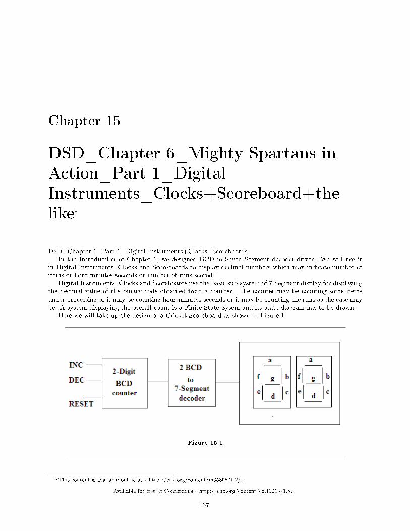
Chapter 15
DSD_Chapter 6_Mighty Spartans in
Action_Part 1_Digital
Instruments_Clocks+Scoreboard+the
like1
DSD_Chapter 6_Part 1_Digital Instruments+Clocks+ScoreboardsIn the Introduction of Chapter 6, we designed BCD-to Seven Segment decoder-driver. We will use it
in Digital Instruments, Clocks and Scoreboards to display decimal numbers which may indicate number ofitems or hour-minutes-seconds or number of runs scored.
Digital Instruments, Clocks and Scoreboards use the basic sub-system of 7-Segment display for displayingthe decimal value of the binary code obtained from a counter. The counter may be counting some itemsunder processing or it may be counting hour-minutes-seconds or it may be counting the runs as the case maybe. A system displaying the overall count is a Finite State Sysem and its state diagram has to be drawn.
Here we will take up the design of a Cricket-Scoreboard as shown in Figure 1.
Figure 15.1
1This content is available online at <http://cnx.org/content/m35855/1.2/>.
Available for free at Connexions <http://cnx.org/content/col11213/1.8>
167

168CHAPTER 15. DSD_CHAPTER 6_MIGHTY SPARTANS IN ACTION_PART
1_DIGITAL INSTRUMENTS_CLOCKS+SCOREBOARD+THE LIKE
Figure 1. The Block Diagram of the Cricket-Scoreboard.6.1.1. Data Path.The scoreboard has three inputs: INC, DEC and RESET.When RESET is TRUE the scoreboard is resetted to �00�. To prevent accidental erasure, RESET must
be pressed for �ve consecutive cycles. Hence there will be a 3-bit reset counter known as rstcnt.When INC is TRUE the score is incremented. When DEC is TRUE the score is decremented. When
INC and DEC, both, are true then no change occurs.There will be two-digit BCD counter which can count from decimal 00 to decimal 99. To display the
two-digit decimal number we wil have two 7-segment displays.There will be two `BCD to 7-segment decoder driver' which will drive the two `7-segment displays'.6.1.2. Controller.The scoreboard will have a INITIALIZATION STATE and a COUNT STATE. Hence there are two well
de�ned States namely S0(Clear State) and S1(Count State). How the state transitions take place are shownin Figure 2 , state diagram, and in Table 1, state table.
Figure 15.2
Figure 2. State Diagram of Cricket Scoreboard displaying the number of runs scored.Table 1. State Table of the scoreboard.
Initial state S0(initialization state) Count State S1(count state)For every clock cycleincrementing or decrementing is done.
continued on next page
Available for free at Connexions <http://cnx.org/content/col11213/1.8>

169
BCD counter is resetted or cleared.RESET<= 0; If rst arrives, rstcnt is incremented. If rstcnt hasreached 4 and rst =1 is persisting this means RE-SET has to done hence system reverts to S0
If inc = 1 and dec = 0, counter is incremented.Add1 indicates that a increment has taken place.
If inc = 0 and dec = 1, counter is decremented.Sub1 indicates that a decrement has taken place.
If rst = 0 then rstcnt is reset.
If { inc=1 and dec=1} or {inc=0 and dec=0} thenrstcnt is resetted and no change in the counter
Table 15.1
6.1.3. VHDL MODEL7-Segment Displays are declared as unsigned 7-bit vectors namely seg7disp0 and seg7disp1.The unsigned vector is used so that overload `+' operator is used for incrementing the counter by 1 and
`-` operator is used for decrementing the counter by 1.The BCD-to-7 Segment decoder driver can be implemented by the following look-up table :Table 2.
Figure 15.3
Available for free at Connexions <http://cnx.org/content/col11213/1.8>

170CHAPTER 15. DSD_CHAPTER 6_MIGHTY SPARTANS IN ACTION_PART
1_DIGITAL INSTRUMENTS_CLOCKS+SCOREBOARD+THE LIKE
Table 2 gives the Look-Up Table. We de�ne a new datatype called SEVSEGARRAY. This datatypede�nes the array of TEN 7-bit vectors corresponding to TEN BCD codes which in turn represent the TENDecimal numbers from `0 to 9' and which are to be displayed on 7-segment displays.
The Look-Up Table has to be addressed by an INTEGER DATA TYPE. We will use conversion function`to_integer' to generate the array index.
Let us consider the expression:`seg7disp0<= seg7rom(to_integer(BCD0))';Here `to_integer(BCD0)' converts BCD0(4-bit vector) to integer type data which is the row index of the
array of 7-bit vectors stored in seg7rom.BCD addition is accomplished with `+' operator.If current BCD0 count is less than 9, it is incremented.If current BCD0 count is 9 then it is resetted and BCD1 is incremented.Reverse logic is applied while decrementing.If BCD0 count is greater than 0, BCD0 is decremented.If BCD0 is zero and BCD1 count is greater than 0 then BCD1 is decremented and BCD0 is assigned 9.Thus the counting proceeds on.Following are the codes for the Cricket Scoreboard.library IEEE;use IEEE.STD_LOGIC_1164.ALL;use IEEE.STD_LOGIC_UNSIGNED.ALL;use IEEE.numeric_bit.all;entity Cricket_scoreboard isPort ( clk : in bit;rst : in bit;inc : in bit;dec : in bit;seg7disp1 : out unsigned(7 downto 1);seg7disp0 : out unsigned(7 downto 1));end Cricket_scoreboard;architecture Behavioral of Cricket_scoreboard issignal state:integer range 0 to 1;signal BCD1, BCD0:unsigned(3 downto 0) := "0000";�unsigned bit vectorsignal rstcnt: integer range 0 to 4 :=0;type sevsegarray is array(0 to 9) of unsigned(6 downto 0);constant seg7Rom: sevsegarray :=("0111111","0000110","1011011","1001111","1100110","1101101","1111100","0000111","1111111","1100111");� active high with "gfedcba" orderbegin______process(clk)______begin___________if clk'event and clk = '1' then_______________________case state is________________________when 0=> �initial state______________________________BCD1 <= "0000";______________________________BCD0 <= "0000";� clear the two decade counters______________________________rstcnt <= 0;� reset RESETCOUNTER______________________________state <= 1;________________________when 1 =>�-state in which scoreboard waits for inc and dec____________________________________if rst = '1' then____________________________________if rstcnt = 4 then � checking whether
5th reset cycle
Available for free at Connexions <http://cnx.org/content/col11213/1.8>

171
____________________________________state <= 0;____________________________________else_________________________________________rstcnt <= rstcnt + 1;____________________________________end if;____________________________________elsif inc = '1' and dec = '0' then____________________________________rstcnt <= 0;____________________________________if BCD0 < "1001" then_________________________________________BCD0 <= BCD0 + 1;� library
with overloaded"+" required____________________________________elsif BCD1 < "1001" then__________________________________________BCD1 <= BCD1 + 1;__________________________________________BCD0 <= "0000";____________________________________end if;_______________________________elsif inc = '0' and dec = '1' then____________________________________rstcnt <= 0;____________________________________if BCD0 > "0000" then___________________________________________BCD0 <= BCD0 - 1;�
library with overloaded"-"required____________________________________elsif BCD1 > "0000" then__________________________________________BCD1 <= BCD1 - 1;__________________________________________BCD0 <= "1001";____________________________________end if;______________________________elsif (inc = '1' and dec = '1') or (inc = '0' and dec
= '0')____________________________________then rstcnt <= 0;______________________________end if;__________________________when others=>null;_____________________end case;_______________end if;__________end process;seg7disp0 <= seg7rom(to_integer(BCD0));�type conversion function fromseg7disp1 <= seg7rom(to_integer(BCD1));�IEEE numeric_bit package usedend behavioral;We carry out the syntax check. After it becomes error free we use Xilinx Synthesis Tool to synthesize
my system.We can view the Synthesis Report.Nexr we view RTL Schematic :
Available for free at Connexions <http://cnx.org/content/col11213/1.8>

172CHAPTER 15. DSD_CHAPTER 6_MIGHTY SPARTANS IN ACTION_PART
1_DIGITAL INSTRUMENTS_CLOCKS+SCOREBOARD+THE LIKE
Figure 15.4
Figure 4. RTL Schematic.Next we look at expanded RTL Schematic.
Available for free at Connexions <http://cnx.org/content/col11213/1.8>

173
Figure 15.5
Figure 5. Expanded RTL Schematic.Next we click at Technology Schematic which is the same as Figure 4. Further clicking gives me Expanded
Technology Schematic as shown in Figure 6 below.
Available for free at Connexions <http://cnx.org/content/col11213/1.8>

174CHAPTER 15. DSD_CHAPTER 6_MIGHTY SPARTANS IN ACTION_PART
1_DIGITAL INSTRUMENTS_CLOCKS+SCOREBOARD+THE LIKE
Figure 15.6
Figure 6.Expanded Technology Schematic.Now we will validate our design by its TEST BENCH.The Test Bench codes are as followed:LIBRARY ieee;use IEEE.STD_LOGIC_1164.ALL;use IEEE.STD_LOGIC_UNSIGNED.ALL;use IEEE.numeric_bit.all;ENTITY TB_Cricket_Scoreboard ISEND TB_Cricket_Scoreboard;ARCHITECTURE test1 OF TB_Cricket_Scoreboard IS� Component Declaration for the Unit Under Test (UUT)COMPONENT Cricket_scoreboardPORT(____clk : IN bit;____ rst : IN bit;____inc : IN bit;____dec : IN bit;____seg7disp1 : OUT unsigned(6 downto 0);
Available for free at Connexions <http://cnx.org/content/col11213/1.8>

175
____seg7disp0 : OUT unsigned(6 downto 0)____);___END COMPONENT;______ type sevsegarray is array (0 to 9) of unsigned(6 downto 0);______constant seg7rom:sevsegarray := ("0111111","0000110","1011011","1001111",______"1100110","1101101","1111100","0000111","1111111","1100111");�Inputs__signal clk : bit := '0';__signal rst : bit := '1';__signal inc : bit := '0';__signal dec : bit := '0';�Outputs__signal seg7disp1 : unsigned(6 downto 0);__signal seg7disp0 : unsigned(6 downto 0);� Clock period de�nitions__constant clk_period : time := 20 ns;BEGIN� Instantiate the Unit Under Test (UUT)uut: Cricket_scoreboard PORT MAP (____clk => clk,____rst => rst,____inc => inc,____dec => dec,____seg7disp1 => seg7disp1,____seg7disp0 => seg7disp0____);� Clock process de�nitionsclk_process :processbegin____________clk <= '0';____________wait for clk_period/2;____________clk <= '1';____________wait for clk_period/2;___end process;� Stimulus process___stim_proc: process___begin� hold rst state for 10 ns.___wait for 20 ns;� insert stimulus here______________________________rst<= '0';______________________________inc<= '1';______________________________dec<= '0';______________________________wait for 20 ns;______________________________rst<= '0';______________________________inc<= '0';______________________________dec<= '0';______________________________wait for 20 ns;______________________________rst<= '0';______________________________inc<= '1';______________________________dec<= '0';
Available for free at Connexions <http://cnx.org/content/col11213/1.8>

176CHAPTER 15. DSD_CHAPTER 6_MIGHTY SPARTANS IN ACTION_PART
1_DIGITAL INSTRUMENTS_CLOCKS+SCOREBOARD+THE LIKE
______________________________wait for 20 ns;______________________________rst<= '0';______________________________inc<= '0';______________________________dec<= '0';______________________________wait for 20 ns;______________________________rst<= '0';______________________________inc<= '1';______________________________dec<= '0';______________________________wait for 20 ns;______________________________rst<= '0';______________________________inc<= '0';______________________________dec<= '0';______________________________wait;_____end process;END;The result of the MODELSIM is given below.
Figure 15.7
Figure 7. The simulated outputs for a given input to the cricket-scoreboard.First Trace is: ClockSecond Trace is : ResetThird Trace is : INCREMENTFourtjh Trace is DECREMENT.Then there are seven traces corresponding to the seven inputs to Display1.Again there are seven traces corresponding to the seven inputs to Display0.As score is incremented the seven inputs of Display1 remains constant at DECIMAL ZERO.Input to Display0 increases from ZERO to ONE to TWO to THREE.This completes the validation of the Cricket-Scoreboard. We can down-load this program on FPGA kit
and connect it to two 7-Segment Displays. The scoreboard is ready for use.
Available for free at Connexions <http://cnx.org/content/col11213/1.8>
INDEX 177
Index of Keywords and Terms
Keywords are listed by the section with that keyword (page numbers are in parentheses). Keywordsdo not necessarily appear in the text of the page. They are merely associated with that section. Ex.apples, � 1.1 (1) Terms are referenced by the page they appear on. Ex. apples, 1
A AND,OR,XOR,NAND, � 7(75)Array,to_integer,unsigned vectors, � 15(167)
B BCD, Seven Segment, Decoder-driver,� 14(161)
D Dual-Gate NMOS,Burn,Voltage Pulse, � 5(43)
E Entity, concurrency, hierarchy, � 6(53)
L Lithography,packing density,smallest featuresize� � 2(3)
M Mealy Machine, State TransitionDiagram,Finite State Machines, � 12(149)MooreMachine,Reset,Clockwise,anti-clockwise,� 11(139)
Moore Machines, Mealy Machines,outputglitches, state diagram, timing diagrams.,� 10(121)Moore's Law., � 2(3)
O Opto Chips, CMOS transceiver, opticalwaveguide, Peta, Exa, � 13(157)
P PLA,PAL,Fixed, Programmable, � 4(27)
S SPLD,CPLD,FPGA,ASIC, � 3(17)
T Testbench,CLK tick event,time patterns,� 8(91)
U Updown Counter, MUX2_1, MUX4_1.,� 9(105)
V VHDL,Verilog,VLSI,FPGA, � 1(1)
Available for free at Connexions <http://cnx.org/content/col11213/1.8>

178 ATTRIBUTIONS
Attributions
Collection: Digital System Design using VHDLEdited by: Bijay_Kumar SharmaURL: http://cnx.org/content/col11213/1.8/License: http://creativecommons.org/licenses/by/3.0/
Module: "EC1561_Syllabus of Digital System Design using VHDL"By: Bijay_Kumar SharmaURL: http://cnx.org/content/m34860/1.4/Page: 1Copyright: Bijay_Kumar SharmaLicense: http://creativecommons.org/licenses/by/3.0/
Module: "Digital System Design_Chapter 1_Part 1-Historical Background of IC Technology."By: Bijay_Kumar SharmaURL: http://cnx.org/content/m34693/1.4/Pages: 3-16Copyright: Bijay_Kumar SharmaLicense: http://creativecommons.org/licenses/by/3.0/
Module: "Digital System_Design_Chapter 1_Part 2_Introduction to VLSI"By: Bijay_Kumar SharmaURL: http://cnx.org/content/m34695/1.3/Pages: 17-26Copyright: Bijay_Kumar SharmaLicense: http://creativecommons.org/licenses/by/3.0/
Module: "DSD_Chapter 2_Basics of PLDs"By: Bijay_Kumar SharmaURL: http://cnx.org/content/m34939/1.3/Pages: 27-41Copyright: Bijay_Kumar SharmaLicense: http://creativecommons.org/licenses/by/3.0/
Module: "Digital System Design_Chapter 2_Section 2_Wishlist of Digital System Designer."By: Bijay_Kumar SharmaURL: http://cnx.org/content/m34940/1.2/Pages: 43-51Copyright: Bijay_Kumar SharmaLicense: http://creativecommons.org/licenses/by/3.0/
Module: "DSD_Chapter 3_VHDL._introduction and content"By: Bijay_Kumar SharmaURL: http://cnx.org/content/m34974/1.1/Pages: 53-73Copyright: Bijay_Kumar SharmaLicense: http://creativecommons.org/licenses/by/3.0/
Available for free at Connexions <http://cnx.org/content/col11213/1.8>

ATTRIBUTIONS 179
Module: "DSD_Chapter 4_VHDL application to combinatorial logic synthesis"By: Bijay_Kumar SharmaURL: http://cnx.org/content/m34984/1.4/Pages: 75-89Copyright: Bijay_Kumar SharmaLicense: http://creativecommons.org/licenses/by/3.0/
Module: "DSD_Chapter 4_VHDL application to sequential logic synthesis"By: Bijay_Kumar SharmaURL: http://cnx.org/content/m34989/1.4/Pages: 91-104Copyright: Bijay_Kumar SharmaLicense: http://creativecommons.org/licenses/by/3.0/
Module: "DSD_Chapter 4_VHDL application to Sequential Circuit Synthesis_Part2"By: Bijay_Kumar SharmaURL: http://cnx.org/content/m35279/1.1/Pages: 105-119Copyright: Bijay_Kumar SharmaLicense: http://creativecommons.org/licenses/by/3.0/
Module: "Chapter 5_ DSD_Moore and Mealy State Machines."By: Bijay_Kumar SharmaURL: http://cnx.org/content/m35681/1.1/Pages: 121-138Copyright: Bijay_Kumar SharmaLicense: http://creativecommons.org/licenses/by/3.0/
Module: "DSD_Chapter 5_StateMachines_Part3_MooreMachine Motor Rotation Sensor Design and Syn-thesis."By: Bijay_Kumar SharmaURL: http://cnx.org/content/m46067/1.1/Pages: 139-148Copyright: Bijay_Kumar SharmaLicense: http://creativecommons.org/licenses/by/3.0/
Module: "DSD_Chapter 5_Part 3_Design of a Mealy Machine_Rotation_Sensor"By: Bijay_Kumar SharmaURL: http://cnx.org/content/m35737/1.2/Pages: 149-155Copyright: Bijay_Kumar SharmaLicense: http://creativecommons.org/licenses/by/3.0/
Module: "DSD_Chapter 5_Supplement_Optical TERA BUS"By: Bijay_Kumar SharmaURL: http://cnx.org/content/m35738/1.1/Pages: 157-159Copyright: Bijay_Kumar SharmaLicense: http://creativecommons.org/licenses/by/3.0/
Available for free at Connexions <http://cnx.org/content/col11213/1.8>

180 ATTRIBUTIONS
Module: "DSD_Chapter 6_Mighty Spartans in Action_Introduction."By: Bijay_Kumar SharmaURL: http://cnx.org/content/m35839/1.1/Pages: 161-166Copyright: Bijay_Kumar SharmaLicense: http://creativecommons.org/licenses/by/3.0/
Module: "DSD_Chapter 6_Mighty Spartans in Action_Part 1_Digital Instru-ments_Clocks+Scoreboard+the like"By: Bijay_Kumar SharmaURL: http://cnx.org/content/m35855/1.2/Pages: 167-176Copyright: Bijay_Kumar SharmaLicense: http://creativecommons.org/licenses/by/3.0/
Available for free at Connexions <http://cnx.org/content/col11213/1.8>

Digital System Design using VHDLEC_1561_[3-1-0] is a 4 hours per week Course to give a hand-on experience on the use of VHDL to designcomplex Digital Systems and implementing them on Xilinx FPGA Component and validating the system.
About ConnexionsSince 1999, Connexions has been pioneering a global system where anyone can create course materials andmake them fully accessible and easily reusable free of charge. We are a Web-based authoring, teaching andlearning environment open to anyone interested in education, including students, teachers, professors andlifelong learners. We connect ideas and facilitate educational communities.
Connexions's modular, interactive courses are in use worldwide by universities, community colleges, K-12schools, distance learners, and lifelong learners. Connexions materials are in many languages, includingEnglish, Spanish, Chinese, Japanese, Italian, Vietnamese, French, Portuguese, and Thai. Connexions is partof an exciting new information distribution system that allows for Print on Demand Books. Connexionshas partnered with innovative on-demand publisher QOOP to accelerate the delivery of printed coursematerials and textbooks into classrooms worldwide at lower prices than traditional academic publishers.