digital saber™ /r - catlog.net part1... · iv list of schematics, circuit boards, and parts lists...
TRANSCRIPT

™ Digital SABER™
and
/R
Portable RadiosDetailed Service Manual

i
Table of Contents
1 - Foreword . . . . . . . . . . . . . . . . . . . . . . . . . . . . . . . . . . . . . . . . . . . . . . . . . . . . . . . . . . . . 1-1
Safety. . . . . . . . . . . . . . . . . . . . . . . . . . . . . . . . . . . . . . . . . . . . . . . . . . . . . . . . . . . . . . . . . . . . . . . .1-1Radio Frequency (RF) Operational Characteristics . . . . . . . . . . . . . . . . . . . . . . . . . . . . . . . . . .1-1Portable Radio Operation and EME Exposure . . . . . . . . . . . . . . . . . . . . . . . . . . . . . . . . . . . . . .1-1Electromagnetic Interference/Compatibility. . . . . . . . . . . . . . . . . . . . . . . . . . . . . . . . . . . . . . .1-3Safety and General. . . . . . . . . . . . . . . . . . . . . . . . . . . . . . . . . . . . . . . . . . . . . . . . . . . . . . . . . . .1-4Operational Warnings . . . . . . . . . . . . . . . . . . . . . . . . . . . . . . . . . . . . . . . . . . . . . . . . . . . . . . . .1-4Operational Cautions . . . . . . . . . . . . . . . . . . . . . . . . . . . . . . . . . . . . . . . . . . . . . . . . . . . . . . . .1-5Intrinsically Safe Radio Information . . . . . . . . . . . . . . . . . . . . . . . . . . . . . . . . . . . . . . . . . . . . .1-5
Manual Revisions . . . . . . . . . . . . . . . . . . . . . . . . . . . . . . . . . . . . . . . . . . . . . . . . . . . . . . . . . . . . . .1-8Computer Software Copyrights . . . . . . . . . . . . . . . . . . . . . . . . . . . . . . . . . . . . . . . . . . . . . . . . . . .1-8Replacement Parts Ordering . . . . . . . . . . . . . . . . . . . . . . . . . . . . . . . . . . . . . . . . . . . . . . . . . . . . . .1-9
Parts Ordering . . . . . . . . . . . . . . . . . . . . . . . . . . . . . . . . . . . . . . . . . . . . . . . . . . . . . . . . . . . . . .1-9Motorola Parts . . . . . . . . . . . . . . . . . . . . . . . . . . . . . . . . . . . . . . . . . . . . . . . . . . . . . . . . . . . . . .1-9Parts Identification . . . . . . . . . . . . . . . . . . . . . . . . . . . . . . . . . . . . . . . . . . . . . . . . . . . . . . . . . .1-9
Portable Radio Model Numbering System . . . . . . . . . . . . . . . . . . . . . . . . . . . . . . . . . . . . . . . . . .1-10ASTRO Digital SABER Detailed Model Chart . . . . . . . . . . . . . . . . . . . . . . . . . . . . . . . . . . . . . . . .1-11Glossary. . . . . . . . . . . . . . . . . . . . . . . . . . . . . . . . . . . . . . . . . . . . . . . . . . . . . . . . . . . . . . . . . . . . .1-12
2 - Introduction . . . . . . . . . . . . . . . . . . . . . . . . . . . . . . . . . . . . . . . . . . . . . . . . . . . . . . . . . 2-1
General . . . . . . . . . . . . . . . . . . . . . . . . . . . . . . . . . . . . . . . . . . . . . . . . . . . . . . . . . . . . . . . . . . . . . .2-1Notations Used in This Manual . . . . . . . . . . . . . . . . . . . . . . . . . . . . . . . . . . . . . . . . . . . . . . . . . . .2-2
3 - General Overview of an ASTRO Digital SABER Radio . . . . . . . . . . . . . . . . . . . . . . . 3-1
Analog Mode of Operation. . . . . . . . . . . . . . . . . . . . . . . . . . . . . . . . . . . . . . . . . . . . . . . . . . . . . . .3-2ASTRO Mode (Digital Mode) of Operation . . . . . . . . . . . . . . . . . . . . . . . . . . . . . . . . . . . . . . . . . . . . . . . . . . . . . . . . . . . . . . . . . .3-2Transceiver Board Overview . . . . . . . . . . . . . . . . . . . . . . . . . . . . . . . . . . . . . . . . . . . . . . . . . . . . . .3-3VOCON Board Overview . . . . . . . . . . . . . . . . . . . . . . . . . . . . . . . . . . . . . . . . . . . . . . . . . . . . . . . .3-3
4 - Radio Power. . . . . . . . . . . . . . . . . . . . . . . . . . . . . . . . . . . . . . . . . . . . . . . . . . . . . . . . . . 4-1
Introduction . . . . . . . . . . . . . . . . . . . . . . . . . . . . . . . . . . . . . . . . . . . . . . . . . . . . . . . . . . . . . . . . . .4-1General . . . . . . . . . . . . . . . . . . . . . . . . . . . . . . . . . . . . . . . . . . . . . . . . . . . . . . . . . . . . . . . . . . . . . .4-1B+ Routing for VHF/UHF Transceiver Boards. . . . . . . . . . . . . . . . . . . . . . . . . . . . . . . . . . . . . . . . .4-2B+ Routing for 800MHz Transceiver Boards. . . . . . . . . . . . . . . . . . . . . . . . . . . . . . . . . . . . . . . . . .4-3B+ Routing for VOCON Boards and Display Modules . . . . . . . . . . . . . . . . . . . . . . . . . . . . . . . . . .4-4
5 - VHF/UHF Transceiver Board Detailed Theory of Operation . . . . . . . . . . . . . . . . . . 5-1
Introduction . . . . . . . . . . . . . . . . . . . . . . . . . . . . . . . . . . . . . . . . . . . . . . . . . . . . . . . . . . . . . . . . . .5-1Frequency Generation Unit (FGU) . . . . . . . . . . . . . . . . . . . . . . . . . . . . . . . . . . . . . . . . . . . . . . . . .5-1Antenna Switch . . . . . . . . . . . . . . . . . . . . . . . . . . . . . . . . . . . . . . . . . . . . . . . . . . . . . . . . . . . . . . .5-3Receiver Front End . . . . . . . . . . . . . . . . . . . . . . . . . . . . . . . . . . . . . . . . . . . . . . . . . . . . . . . . . . . . .5-3Receiver Back End . . . . . . . . . . . . . . . . . . . . . . . . . . . . . . . . . . . . . . . . . . . . . . . . . . . . . . . . . . . . . .5-4Transmitter . . . . . . . . . . . . . . . . . . . . . . . . . . . . . . . . . . . . . . . . . . . . . . . . . . . . . . . . . . . . . . . . . . .5-5
Harmonic Filter . . . . . . . . . . . . . . . . . . . . . . . . . . . . . . . . . . . . . . . . . . . . . . . . . . . . . . . . . . . . .5-5RF Power Amplifier Module. . . . . . . . . . . . . . . . . . . . . . . . . . . . . . . . . . . . . . . . . . . . . . . . . . . .5-5ALC Circuits. . . . . . . . . . . . . . . . . . . . . . . . . . . . . . . . . . . . . . . . . . . . . . . . . . . . . . . . . . . . . . . .5-5
A
, Motorola, ASTRO, Private-Line, and Digital Private Line are trademarks of Motorola, Inc.© 2000, 2001 MotorolaCommercial, Government, Industrial Solutions Sector8000 W. Sunrise Blvd., Fort Lauderdale, FL 33322All Rights Reserved. Printed in U. S. A. 4/2001.
Detailed Service Manual68P81076C10-A

ii
6 - 800MHz Transceiver Board Detailed Theory of Operation . . . . . . . . . . . . . . . . . . . 6-1
Introduction . . . . . . . . . . . . . . . . . . . . . . . . . . . . . . . . . . . . . . . . . . . . . . . . . . . . . . . . . . . . . . . . . 6-1Frequency Synthesis . . . . . . . . . . . . . . . . . . . . . . . . . . . . . . . . . . . . . . . . . . . . . . . . . . . . . . . . . . . 6-1Antenna Switch. . . . . . . . . . . . . . . . . . . . . . . . . . . . . . . . . . . . . . . . . . . . . . . . . . . . . . . . . . . . . . . 6-2Receiver Front End . . . . . . . . . . . . . . . . . . . . . . . . . . . . . . . . . . . . . . . . . . . . . . . . . . . . . . . . . . . . 6-3Receiver Back End . . . . . . . . . . . . . . . . . . . . . . . . . . . . . . . . . . . . . . . . . . . . . . . . . . . . . . . . . . . . . 6-4Transmitter . . . . . . . . . . . . . . . . . . . . . . . . . . . . . . . . . . . . . . . . . . . . . . . . . . . . . . . . . . . . . . . . . . 6-5
7 - VOCON Board Detailed Theory of Operation. . . . . . . . . . . . . . . . . . . . . . . . . . . . . . . 7-1
Introduction . . . . . . . . . . . . . . . . . . . . . . . . . . . . . . . . . . . . . . . . . . . . . . . . . . . . . . . . . . . . . . . . . 7-1General . . . . . . . . . . . . . . . . . . . . . . . . . . . . . . . . . . . . . . . . . . . . . . . . . . . . . . . . . . . . . . . . . . . . . 7-1Controller Section. . . . . . . . . . . . . . . . . . . . . . . . . . . . . . . . . . . . . . . . . . . . . . . . . . . . . . . . . . . . . 7-2Vocoder Section . . . . . . . . . . . . . . . . . . . . . . . . . . . . . . . . . . . . . . . . . . . . . . . . . . . . . . . . . . . . . . 7-3Switched Regulator . . . . . . . . . . . . . . . . . . . . . . . . . . . . . . . . . . . . . . . . . . . . . . . . . . . . . . . . . . . . 7-5RX Signal Path. . . . . . . . . . . . . . . . . . . . . . . . . . . . . . . . . . . . . . . . . . . . . . . . . . . . . . . . . . . . . . . . 7-6TX Signal Path. . . . . . . . . . . . . . . . . . . . . . . . . . . . . . . . . . . . . . . . . . . . . . . . . . . . . . . . . . . . . . . . 7-8Controller Bootstrap and Asynchronous Buses . . . . . . . . . . . . . . . . . . . . . . . . . . . . . . . . . . . . . 7-10Vocoder Bootstrap. . . . . . . . . . . . . . . . . . . . . . . . . . . . . . . . . . . . . . . . . . . . . . . . . . . . . . . . . . . . 7-11SPI Bus Interface . . . . . . . . . . . . . . . . . . . . . . . . . . . . . . . . . . . . . . . . . . . . . . . . . . . . . . . . . . . . . 7-12Universal Connector and Option Selects . . . . . . . . . . . . . . . . . . . . . . . . . . . . . . . . . . . . . . . . . . 7-12Keypad and Display Module. . . . . . . . . . . . . . . . . . . . . . . . . . . . . . . . . . . . . . . . . . . . . . . . . . . . 7-13Controls and Control Top Flex. . . . . . . . . . . . . . . . . . . . . . . . . . . . . . . . . . . . . . . . . . . . . . . . . . 7-14Controller Memory Map. . . . . . . . . . . . . . . . . . . . . . . . . . . . . . . . . . . . . . . . . . . . . . . . . . . . . . . 7-15Vocoder Memory Map . . . . . . . . . . . . . . . . . . . . . . . . . . . . . . . . . . . . . . . . . . . . . . . . . . . . . . . . 7-17MCU System Clock . . . . . . . . . . . . . . . . . . . . . . . . . . . . . . . . . . . . . . . . . . . . . . . . . . . . . . . . . . . 7-19DSP System Clock . . . . . . . . . . . . . . . . . . . . . . . . . . . . . . . . . . . . . . . . . . . . . . . . . . . . . . . . . . . . 7-19Radio Power-Up/Power-Down Sequence . . . . . . . . . . . . . . . . . . . . . . . . . . . . . . . . . . . . . . . . . . 7-19
8 - Secure Modules . . . . . . . . . . . . . . . . . . . . . . . . . . . . . . . . . . . . . . . . . . . . . . . . . . . . . . . 8-1
Introduction . . . . . . . . . . . . . . . . . . . . . . . . . . . . . . . . . . . . . . . . . . . . . . . . . . . . . . . . . . . . . . . . . 8-1Circuit Description . . . . . . . . . . . . . . . . . . . . . . . . . . . . . . . . . . . . . . . . . . . . . . . . . . . . . . . . . . . . 8-2TroubleshootingSecure Operations . . . . . . . . . . . . . . . . . . . . . . . . . . . . . . . . . . . . . . . . . . . . . . . . . . . . . . . . . . . . . 8-2
Error 09/10, Error 09/90 . . . . . . . . . . . . . . . . . . . . . . . . . . . . . . . . . . . . . . . . . . . . . . . . . . . . . . . . . . . . . . . . 8-2Keyload. . . . . . . . . . . . . . . . . . . . . . . . . . . . . . . . . . . . . . . . . . . . . . . . . . . . . . . . . . . . . . . . . . . 8-2
9 - Troubleshooting Procedures . . . . . . . . . . . . . . . . . . . . . . . . . . . . . . . . . . . . . . . . . . . . 9-1
Introduction . . . . . . . . . . . . . . . . . . . . . . . . . . . . . . . . . . . . . . . . . . . . . . . . . . . . . . . . . . . . . . . . . 9-1Handling Precautions . . . . . . . . . . . . . . . . . . . . . . . . . . . . . . . . . . . . . . . . . . . . . . . . . . . . . . . . . . 9-1Voltage Measurement and Signal Tracing . . . . . . . . . . . . . . . . . . . . . . . . . . . . . . . . . . . . . . . . . . 9-2Power-Up Self-Check Errors . . . . . . . . . . . . . . . . . . . . . . . . . . . . . . . . . . . . . . . . . . . . . . . . . . . . . 9-3
Power-Up Sequence . . . . . . . . . . . . . . . . . . . . . . . . . . . . . . . . . . . . . . . . . . . . . . . . . . . . . . . . . 9-3Standard Bias Table . . . . . . . . . . . . . . . . . . . . . . . . . . . . . . . . . . . . . . . . . . . . . . . . . . . . . . . . . . . . 9-6
10 - Troubleshooting Charts . . . . . . . . . . . . . . . . . . . . . . . . . . . . . . . . . . . . . . . . . . . . . . 10-1
11 - Troubleshooting Waveforms. . . . . . . . . . . . . . . . . . . . . . . . . . . . . . . . . . . . . . . . . . 11-1
Introduction . . . . . . . . . . . . . . . . . . . . . . . . . . . . . . . . . . . . . . . . . . . . . . . . . . . . . . . . . . . . . . . . 11-1Waveforms . . . . . . . . . . . . . . . . . . . . . . . . . . . . . . . . . . . . . . . . . . . . . . . . . . . . . . . . . . . . . . . . . 11-1
12 - Troubleshooting Diagrams . . . . . . . . . . . . . . . . . . . . . . . . . . . . . . . . . . . . . . . . . . . 12-1
Introduction to This Section. . . . . . . . . . . . . . . . . . . . . . . . . . . . . . . . . . . . . . . . . . . . . . . . . . . . 12-1
13 - Block Diagrams, Schematics, Electrical Parts Lists, and Circuit Board Details 13-1

iii
List of Figures
Figure 1 . B+ Routing for VHF/UHF Transceiver Boards.................................................................. 4-2
Figure 2. B+ Routing for 800MHz Transceiver Boards.................................................................... 4-3
Figure 3. B+ Routing for Vocoder/Controller (VOCON) Boards .................................................... 4-5
Figure 4. VOCON Board - Controller Section................................................................................. 7-2
Figure 5. VOCON Board - Vocoder Section .................................................................................... 7-4
Figure 6. DSP RSSI Port - RX Mode ................................................................................................. 7-6
Figure 7. DSP RSSI Port - TX Mode ................................................................................................. 7-8
Figure 8. Host SB9600 and RS232 Ports ........................................................................................ 7-10
Figure 9. Universal Connector...................................................................................................... 7-12
Figure 10. VOCON Board Connector - J201................................................................................... 7-12
Figure 11. Control Top Flex ............................................................................................................ 7-14
Figure 12. Controller Memory Mapping ........................................................................................ 7-16
Figure 13. Vocoder Memory Mapping............................................................................................ 7-18
Figure 14. Waveform W1................................................................................................................ 11-1
Figure 15. Waveform W2................................................................................................................ 11-2
Figure 16. Waveform W3................................................................................................................ 11-2
Figure 17. Waveform W4................................................................................................................ 11-3
Figure 18. Waveform W5................................................................................................................ 11-3
Figure 19. Waveform W6................................................................................................................ 11-4
Figure 20. Waveform W7................................................................................................................ 11-4
Figure 21. Waveform W8................................................................................................................ 11-5
Figure 22. Waveform W9................................................................................................................ 11-5
Figure 23. Waveform W10.............................................................................................................. 11-6
List of Tables
Table 1. Option Select Functions................................................................................................. 7-13
Table 2. Standard Operating Bias .................................................................................................. 9-6
Table 3. J201 VOCON Board to Universal Connector ................................................................ 12-1
Table 4. J601VOCON Board to Display Board ............................................................................ 12-2
Table 5. J701 VOCON Board to Keypad ...................................................................................... 12-2
Table 6. J1/J401 Transceiver Board to VOCON Board................................................................. 12-2
Table 7. J801 VOCON Board to Encryption Board ..................................................................... 12-3
Table 8. J901 VOCON Board to Control Top Flex ...................................................................... 12-3

iv
List of Schematics, Circuit Boards, and Parts Lists
Radio Interconnect Diagram............................................................................................................ 13-2
NLD8892R VHF Transceiver Board Schematic Diagram.................................................................. 13-3
NLD8892R VHF Transceiver Circuit Board Details and Parts List ................................................... 13-4
NLE4560K UHF Range 1 Transceiver Board Schematic Diagram .................................................... 13-6
NLE4560K UHF Range 1 Transceiver Circuit Board Details and Parts List ..................................... 13-7
NLE4244P UHF Range 2 Transceiver Board Schematic Diagram .................................................... 13-9
NLE4244P UHF Range 2 Transceiver Circuit Board Details and Parts List.................................... 13-10
NUF6411K 800 MHz Transceiver Board Schematic Diagram........................................................ 13-12
NUF6411K 800 MHz Transceiver Circuit Board Details and Parts List ......................................... 13-13
NTN7749G VOCON (Vocoder/Controller) Board Schematic Diagram, Sheet 1 of 2.................... 13-16
NTN7749G VOCON (Vocoder/Controller) Board Schematic Diagram, Sheet 2 of 2.................... 13-17
NTN7749G VOCON (Vocoder/Controller) Circuit Board Details & Parts List.................... 13-18
Related Publications
ASTRO Digital SABER (Model I) User’s Guide . . . . . . . . . . . . . . . . . . . . . . . . . . . . . . . . . .68P81072C75
ASTRO Digital SABER (Models II and III) User’s Guide . . . . . . . . . . . . . . . . . . . . . . . . . .68P81072C80
ASTRO Digital SABER Portable Radios Basic Service Manual . . . . . . . . . . . . . . . . . . . . . .68P81076C05

1-1
Foreword
1
Safety
SAFETY AND GENERAL INFORMATION
IMPORTANT INFORMATION ON SAFE AND EFFICIENT OPERATION
READ THIS INFORMATION BEFORE USING YOUR MOTOROLA TWO-WAY RADIO
The information provided in this document supersedes the general safety information contained in user guides published prior to October 2000. For information regarding radio use in a hazardous atmosphere refer to the Factory Mutual (FM) manual supplement included with radio models that offer this capability and/or the intrinsic safety radio information section of this user manual.
Radio Frequency (RF) Operational Characteristics
To transmit (talk) you must push the Push-To-Talk button; to receive (listen) you must release the Push-To-Talk button.
When the radio is transmitting, it generates radio frequency (RF) energy; when it is receiving, or when it is off, it does not generate RF energy.
Portable Radio Operation and EME Exposure
Your Motorola radio is designed to comply with the following national and international standards and guidelines regarding exposure of human beings to radio frequency electromagnetic energy (EME):
•
United States Federal Communications Commission, Code of Federal Regulations; 47 CFR part 2 sub-part J
•
American National Standards Institute (ANSI) / Institute of Electrical and Electronic Engineers (IEEE) C95. 1-1992
•
Institute of Electrical and Electronic Engineers (IEEE) C95.1-1999 Edition
•
National Council on Radiation Protection and Measurements (NCRP) of the United States, Report 86, 1986
•
International Commission on Non-Ionizing Radiation Protection (ICNIRP) 1998
•
Ministry of Health (Canada) Safety Code 6. Limits of Human

1-2
Exposure to Radio Frequency Electromagnetic Fields in the Frequency Range from 3 kHz to 300 GHz, 1999
•
Australian Communications Authority Radiocommunications (Electromagnetic Radiation - Human Exposure) Standard 1999 (applicable to wireless phones only)
To assure optimal radio performance and make sure human exposure to radio frequency electromagnetic energy is within the guidelines set forth in the above standards, always adhere to the following procedures:
Two-way Radio Operation
Body-worn Operation
To maintain compliance with FCC RF exposure guidelines, if you wear a radio on your body when transmitting, always place the radio in
a Motorola approved clip, holder, holster, case, or body harness for this product
. Use of non-Motorola-approved accessories may exceed FCC RF exposure guidelines.
If you do not use a Motorola approved body-worn accessory and are not using the radio in the intended use positions along side of the head in the phone mode or in front of the face in the two-way radio mode, then ensure the antenna and radio is kept the following minimum distances from the body when transmitting:
•
Phone or Two-way radio mode: one inch (2.5 centimeters)
•
Data operation using any data feature with or without an accessory cable: one inch (2.5 centimeters)
Antenna Care
Use only the supplied or an approved replacement antenna.
Unauthorized antennas, modifications, or attachments could damage the radio and may violate FCC regulations.
DO NOT hold the antenna when the radio is “IN USE”.
Holding the antenna affects call quality and may cause the radio to operate at a higher power level than needed.
Approved Accessories
For a list of approved Motorola accessories look in the appendix or accessory section of your radio’s User Guide.
When using your radio,
hold the radio in a vertical position with the microphone one to two inches (2.5 to 5 centimeters) away from the lips.
MAN WITH RA

1-3
Electromagnetic Interference/Compatibility
NOTE:
Nearly every electronic device is susceptible to electromagnetic interference (EMI) if inadequately shielded, designed or otherwise configured for electromagnetic compatibility.
Facilities
To avoid electromagnetic interference and/or compatibility conflicts, turn off your radio in any facility where posted notices instruct you to do so. Hospitals or health care facilities may be using equipment that is sensitive to external RF energy.
Aircraft
When instructed to do so, turn off your radio when on board an aircraft. Any use of a radio must be in accordance with applicable regulations per airline crew instructions.
Medical Devices
•
Pacemakers
The Health Industry Manufacturers Association recommends that a minimum separation of 6 inches (15 centimeters) be maintained between a handheld wireless radio and a pacemaker.These recommendations are consistent with those of the U.S. Food and Drug Administration.
Persons with pacemakers should:
•
ALWAYS keep the radio more than 6 inches (15 centimeters) from their pacemaker when the radio is turned ON.
•
not carry the radio in the breast pocket.
•
use the ear opposite the pacemaker to minimize the potential for interference.
•
turn the radio OFF immediately if you have any reason to suspect that interference is taking place.
•
Hearing Aids
Some digital wireless radios may interfere with some hearing aids. In the event of such interference, you may want to consult your hearing aid manufacturer to discuss alternatives.
•
Other Medical Devices
If you use any other personal medical device, consult the manufacturer of your device to determine if it is adequately shielded from RF energy. Your physician may be able to assist you in obtaining this information.
1-4
SAFETY AND GENERAL
Use While Driving
Check the laws and regulations on the use of radios in the area where you drive. Always obey them.
When using your radio while driving, please:
•
Give full attention to driving and to the road.
•
Use hands-free operation, if available.
•
Pull off the road and park before making or answering a call if driving conditions so require.
OPERATIONAL WARNINGS
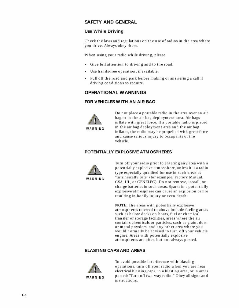
FOR VEHICLES WITH AN AIR BAG
POTENTIALLY EXPLOSIVE ATMOSPHERES
BLASTING CAPS AND AREAS
Do not place a portable radio in the area over an air bag or in the air bag deployment area. Air bags inflate with great force. If a portable radio is placed in the air bag deployment area and the air bag inflates, the radio may be propelled with great force and cause serious injury to occupants of the vehicle.
Turn off your radio prior to entering any area with a potentially explosive atmosphere, unless it is a radio type especially qualified for use in such areas as "Intrinsically Safe" (for example, Factory Mutual, CSA, UL, or CENELEC). Do not remove, install, or charge batteries in such areas. Sparks in a potentially explosive atmosphere can cause an explosion or fire resulting in bodily injury or even death.
NOTE:
The areas with potentially explosive atmospheres referred to above include fueling areas such as below decks on boats, fuel or chemical transfer or storage facilities, areas where the air contains chemicals or particles, such as grain, dust or metal powders, and any other area where you would normally be advised to turn off your vehicle engine. Areas with potentially explosive atmospheres are often but not always posted.
To avoid possible interference with blasting operations, turn off your radio when you are near electrical blasting caps, in a blasting area, or in areas posted: "Turn off two-way radio.” Obey all signs and instructions.
!W A R N I N G
!
!W A R N I N G
!
!W A R N I N G
!

1-5
OPERATIONAL CAUTIONS
ANTENNAS
BATTERIES
INTRINSICALLY SAFE RADIO INFORMATION
FMRC Approved Equipment
Anyone intending to use a radio in a location where hazardous concentrations of flammable material exist (hazardous atmosphere) is advised to become familiar with the subject of intrinsic safety and with the National Electric Code NFPA 70 (National Fire Protection Association) Article 500 (hazardous [classified] locations).
An Approval Guide, issued by Factory Mutual Research Corporation (FMRC), lists manufacturers and the products approved by FMRC for use in such locations. FMRC has also issued a voluntary approval standard for repair service (“Class Number 3605”).
FMRC Approval labels are attached to the radio to identify the unit as being FM Approved for specified hazardous atmospheres. This label specifies the hazardous Class/Division/Group along with the part number of the battery that must be used. Depending on the design of the portable unit, this FM label can be found on the back or the bottom of the radio housing. The FM Approval mark is shown below:
Do not use any portable radio that has a damaged antenna.
If a damaged antenna comes into contact with your skin, a minor burn can result.
All batteries can cause property damage and/or bodily injury such as burns if a conductive material such as jewelry, keys, or beaded chains touch exposed terminals. The conductive material may complete an electrical circuit (short circuit) and become quite hot. Exercise care in handling any charged battery, particularly when placing it inside a pocket, purse, or other container with metal objects.
!C a u t i o n
!C a u t i o n
FM
APPROVED

1-6
WARNINGS
WARNINGS
•
Do not operate radio communications equipment in a hazardous atmosphere unless it is a type especially qualified for such use (e.g., FMRC Approved). An explosion or fire may result.
•
Do not operate an FMRC Approved Product in a hazardous atmosphere if it has been physically damaged (e.g., cracked housing). An explosion or fire may result.
•
Do not replace or charge batteries in a hazardous atmosphere. Contact sparking may occur while installing or removing batteries and cause an explosion or fire.
•
Do not replace or change accessories in a hazardous atmosphere. Contact sparking may occur while installing or removing accessories and cause an explosion or fire.
•
Do not operate an FMRC Approved Product unit in a hazardous location with the accessory contacts exposed. Keep the connector cover in place when accessories are not used.
•
Turn a radio off before removing or installing a battery or accessory.
•
Do not disassemble an FMRC Approved Product unit in any way that exposes the internal electrical circuits of the unit.
•
Radios must ship from the Motorola manufacturing facility with the hazardous atmosphere capability and FM Approval labeling. Radios will not be “upgraded” to this capability and labeled in the field.
• A modification changes the unit’s hardware from its original design configuration. Modifications can only be made by the original product manufacturer at one of its FMRC-audited manufacturing facilities.
!W A R N I N G
!
!W A R N I N G
!

1-7
WARNINGS
Repair of FMRC Approved Products
REPAIRS FOR MOTOROLA PRODUCTS WITH FMRC APPROVAL ARE THE RESPONSIBILITY OF THE USER.
You should not repair or relabel any Motorola- manufactured communication equipment bearing the FMRC Approval label (“FMRC Approved Product”) unless you are familiar with the current FMRC Approval standard for repairs and service (“Class Number 3605”).
You may want to consider using a repair facility that operates under 3605 repair service approval.
WARNINGS
FMRC’s Approval Standard Class Number 3605 is subject to change at any time without notice to you, so you may want to obtain a current copy of 3605 from FMRC. Per the December 1994 publication of 3605, some key definitions and service requirements are as follows:
Repair
A repair constitutes something done internally to the unit that would bring it back to its original condition—Approved by FMRC. A repair should be done in an FMRC Approved facility.
Items not considered as repairs are those in which an action is performed on a unit which does not require the outer casing of the unit to be opened in a manner which exposes the internal electrical circuits of the unit. You do not have to be an FMRC Approved Repair Facility to perform these actions.
• Failure to use an FMRC Approved Product unit with an FMRC Approved battery or FMRC Approved accessories specifically approved for that product may result in the dangerously unsafe condition of an unapproved radio combination being used in a hazardous location.
• Unauthorized or incorrect modification of an FMRC Approved Product unit will negate the Approval rating of the product.
• Incorrect repair or relabeling of any FMRC Approved Product unit could adversely affect the Approval rating of the unit.
• Use of a radio that is not intrinsically safe in a hazardous atmosphere could result in serious injury or death.
!W A R N I N G
!
!W A R N I N G
!

1-8
Relabeling
The repair facility shall have a method by which the replacement of FMRC Approval labels are controlled to ensure that any relabeling is limited to units that were originally shipped from the Manufacturer with an FM Approval label in place. FMRC Approval labels shall not be stocked by the repair facility. An FMRC Approval label shall be ordered from the original manufacturer, as needed, to repair a specific unit. Replacement labels may be obtained and applied by the repair facility, provided there is satisfactory evidence that the unit being relabeled was originally an FMRC Approved unit. Verification may include, but is not limited to: a unit with a damaged Approval label, a unit with a defective housing displaying an Approval label, or a customer invoice indicating the serial number of the unit and purchase of an FMRC Approved model.
Do Not Substitute Options or Accessories
The Motorola communications equipment certified by Factory Mutual is tested as a system and consists of the FM Approved portable, FM Approved battery, and FM Approved accessories or options, or both. This FM Approved portable and battery combination must be strictly observed. There must be no substitution of items, even if the substitute has been previously Approved with a different Motorola communications equipment unit. Approved configurations are listed in the FM Approval Guide published by FMRC, or in the product FM Supplement. This FM Supplement is shipped from the manufacturer with the FM Approved radio and battery combination. The Approval Guide, or the Approval Standard Class Number 3605 document for repairs and service, can be ordered directly from Factory Mutual Research Corporation located in Norwood, Massachusetts.
Manual Revisions Changes which occur after this manual is printed are described in “FMRs.” These FMRs provide complete information on changes including pertinent parts listing data.
Computer Software Copyrights
The Motorola products described in this manual may include copyrighted Motorola computer programs stored in semiconductor memories or other media. Laws in the United States and other countries preserve for Motorola certain exclusive rights for copyrighted computer programs, including the exclusive right to copy or reproduce in any form the copyrighted computer program. Accordingly, any copyrighted Motorola computer programs contained in the Motorola products described in this manual may not be copied or reproduced in any manner without the express written permission of Motorola. Furthermore, the purchase of Motorola products shall not be deemed to grant either directly or by implication, estoppel, or otherwise, any license under the copyrights, patents or patent applications of Motorola, except for the normal non-exclusive royalty free license to use that arises by operation of law in the sale of a product.

1-9
Replacement Parts Ordering
When ordering replacement parts or equipment information, the complete identification number should be included. This applies to all components, kits, and chassis. If the component part number is not known, the order should include the number of the chassis or kit of which it is a part, and sufficient description of the desired component to identify it.
Crystal and channel element orders should specify the crystal or channel element type number, crystal and carrier frequency, and the model number in which the part is used.
Parts Ordering 7:00 A. M. to 7:00 P. M. (Central Standard Time)Monday through Friday (Chicago, U. S. A.)Domestic (U. S. A.): 1-800-422-420, or 847-538-80231-800-826-1913, or 410-712-6200 (Federal Government)TELEX: 280127FAX: 1-847-538-8198FAX: 1-410-712-4991 (Federal Government)Domestic (U. S. A.) after hours or weekends:1-800-925-4357International: 1-847-538-8023
Motorola Parts Accessories and Aftermarket Division(United States and Canada)Attention: Order Processing1313 E. Algonquin RoadSchaumburg, IL 60196
Accessories and Aftermarket DivisionAttention: International Order Processing1313 E. Algonquin RoadSchaumburg, IL 60196
Parts Identification 1-847-538-0021 (Voice)1-847-538-8194 (FAX)

1-10
Portable Radio Model Numbering System
Position 1 - Type of Unit
H = Hand-Held Portable
Positions 2 & 3 - Model Series
Position 4 - Frequency BandLess than 29.7MHz29.7 to 35.99MHz36 to 41.99MHz42 to 50MHz66 to 80MHz74 to 90MHzProduct Specific136 to 162MHz146 to 178MHz174 to 210MHz190 to 235MHz
336 to 410MHz403 to 437MHz438 to 482MHz470 to 520MHzProduct Specific806 to 870MHz825 to 870MHz896 to 941MHz1.0 to 1.6GHz1.5 to 2.0GHz
Values given represent range only; they arenot absolute.
Position 5 - Power Level0 to 0.7 Watts0.7 to 0.9 Watts1.0 to 3.9 Watts4.0 to 5.0 Watts5.1 to 6.0 Watts6.1 to 10 Watts
Position 6 - Physical Packages
RF Modem OperationReceiver OnlyStandard Control; No DisplayStandard Control; With DisplayLimited Keypad; No DisplayLimited Keypad; With DisplayFull Keypad; No DisplayFull Keypad; With DisplayLimited Controls; No DisplayLimited Controls; Basic DisplayLimited Controls; Limited DisplayRotary Controls; Standard DisplayEnhanced Controls; Enhanced DisplayLow Profile; No DisplayLow Profile; Basic DisplayLow Profile; Basic Display, Full Keypad
Position 7 - Channel Spacing1 = 5kHz2 = 6.25kHz3 = 10kHz4 = 12.5kHz
5 = 15kHz6 = 20/25kHz7 = 30kHz9 = Variable/Programmable
Typical Model Number:Position:
Position 8 - Primary OperationConventinal/SimplexConventional/DuplexTrunked Twin TypeDual Mode TrunkedDual Mode Trunked/DuplexTrunked Type ITrunked Type IIFDMA* Digital Dual ModeTDMA** Digital Dual ModeSingle SidebandGlobal Positioning Satellite CapableAmplitude Companded Sideband (ACSB)Programmable
* FDMA = Frequency Division Multiple Access** TDMA = Time Division Multiple Access
Position 9 - Primary System TypeConventionalPrivacy Plus®Clear SMARTNET™Advanced Conventional Stat-Alert™Enhanced Privacy Plus®Nauganet 888 SeriesJapan Specialized Mobile Radio (JSMR)Multi-Channel Access (MCA)CoveragePLUS™MPT1327* - PublicMPT1327* - PrivateRadiocomTone SignallingBinary SignallingPhonenet®ProgrammableSecure ConventionalSecure SMARTNET™
* MPT = Ministry of Posts and Telecommunications
Position 10 - Feature Level1 = Basic2 = Limited Package3 = Limited Plus4 = Intermediate5 = Standard Package
6 = Standard Plus7 = Expanded Package8 = Expanded Plus9 = Full Feature/ Programmable
Position 11 - VersionVersion Letter (Alpha) - Major Change
Position 12 - Unique Model VariationsC = CenelecN = Standard Package
Positions 13 - 16“SP” Model Suffix
1 2 3 4 5 6 7 8 9 10 11 12 13 14 15 16H 0 4 U C F 9 P W 7 A N S P 0 1
04 = ASTRO
ABCDFGHJKLM
===========
PQRSTUVWYZ
==========
A BCDEF
======
A BCDEFGHJKLMNPQR
================
A BCDEFGHJKLMP
=============
A BCDEFGHJKLMNPQWXY
==================

1-11
ASTRO Digital SABER Detailed Model Chart
Model Number Description
H04KDC9PW5AN VHF 1-5 Watt ASTRO Digital SABER Model I
H04KDF9PW7AN VHF 1-5 Watt ASTRO Digital SABER Model II
H04KDH9PW7AN VHF 1-5 Watt ASTRO Digital SABER Model III
H04RDC9PW5AN UHF 1-4 Watt ASTRO Digital SABER Model I
H04RDF9PW7AN UHF 1-4 Watt ASTRO Digital SABER Model II
H04RDH9PW7AN UHF 1-4 Watt ASTRO Digital SABER Model III
H04SDC9PW5AN UHF 1-4 Watt ASTRO Digital SABER Model I
H04SDF9PW7AN UHF 1-4 Watt ASTRO Digital SABER Model II
H04SDH9PW7AN UHF 1-4 Watt ASTRO Digital SABER Model III
H04UCC9PW5AN 800MHz 1-3 Watt ASTRO Digital SABER Model I
H04UCF9PW7AN 800MHz 1-3 Watt ASTRO Digital SABER Model II
H04UCH9PW7AN 800MHz 1-3 Watt ASTRO Digital SABER Model III
Item Number Description
X X X X NHN6544_ Housing (with display and 3 x 6 keypad)
X X X X NHN6554_ Housing (with display and 3 x 2 keypad)
X X X X NHN6555_ Housing (no display and no keypad)
X X X NLD8892_ VHF Transceiver Board (136-174MHz)
X X X NLE4560_ UHF Transceiver Board (403-470MHz)
X X X NLE4244_ UHF Transceiver Board (450-512MHz)
X X X NUF6411_ 800MHz Transceiver Board (806-870MHz)
X X X X X X X X X X X X NTN4595_ Nickel-Cadmium, Ultra-High Capacity (1800mAh), Large-Size Housing (Height 3.9” ) Battery
X X X X X X X X X X X X NTN7061_ Accessory Connector Cover
X X X X X X X X X X X X NTN7268_ Control Top Chassis
X X X X X X X X X X X X NTN7309_ Belt Clip
X X X X NTN7637_ Non-Display Front Shield
X X X X X X X X NTN7638_ Display Front Shield
X X X X X X X X X X X X NTN7749_ VOCON Kit
X X X X X X X X X X X X 0305150X01 VOCON Shield Screws (qty. 4)
X X X X X X X X X X X X 1302646J01 Control Top Escutcheon
X X X X X X X X X X X X 1302647J01 16-Position Select Knob Escutcheon
X X X X X X X X X X X X 2605403X01 VOCON Board Back Shield
X X X X X X X X X X X X 2605535W02 Center Transceiver Shield
X X X X X X X X X X X X 2605844V01 VOCON Board Top Shield
X X X X X X X X X X X X 2805462X01 20-Pin Mating Plug
X X X X X X X X X X X X 3205082E48 On/Off/Volume Control Knob O-Ring Gasket
X X X X X X X X X X X X 3205082E80 Control Top O-Ring Gasket
X X X X X X X X X X X X 3205082E83 Programmable Button O-Ring Gasket
X X X X X X X X X X X X 4502640J01 2-Position A/B Switch
X X X 8505518V01 VHF Antenna
X X X X X X 8505241U05 UHF Antenna
X X X 8505241U03 800MHz Antenna
X = Indicates one of each is required.

1-12
Glossary
A/D Analog to Digital converter; converts an instantaneous dc voltage level to a corresponding digital value.
ABACUS IC Custom integrated circuit providing a digital receiver IF backend.
ADSIC ABACUS/DSP Support IC; custom integrated circuit providing peripheral functions for the DSP.
ALC Automatic Level Control; a circuit in the transmit RF path that controls RF power amplifier output, provides leveling over frequency and voltage, and protects against high VSWR.
D/A Digital to Analog converter; converts a digital value to a corresponding dc voltage value.
DTMF Dual Tone Multi-Frequency
DPL Digital Private-Line™
DSP Digital Signal Processor; microcontroller specifically tailored for signal processing computations. In this case refers specifically to Motorola DSP56001.
Firmware Software or a software/hardware combination of computer programs and data, with a fixed logic configuration stored in a read-only memory; information can not be altered or reprogrammed.
FGU Frequency Generation Unit
FLASHport™ A Motorola term that describes the ability of a radio to change memory. Every FLASHport radio contains a FLASHport EEPROM memory chip that can be software written and rewritten to, again and again.
Host Motorola HC11F1 microcontrol unit U204 (see MCU).
Host Port Parallel memory mapped interface consisting of eight registers in the DSP56001.
IC Integrated Circuit
IMBE A sub-band, voice encoding algorithm used in ASTRO digital voice.
ISW Inbound Signalling Word; data transmitted on the control channel from a subscriber unit to the central control unit.
LSH Low Speed Handshake; 150 baud digital data sent to the radio during trunked operation while receiving audio.
MCU MicroControl Unit
MDC Motorola Digital Communications
OMPAC Over-Molded Pad-Array Carrier; a Motorola custom IC package, distinguished by the presence of solder balls on the bottom pads.
Open Architecture A controller configuration that utilizes a microprocessor with extended ROM, RAM, and EEPROM.
OSW Outbound Signalling Word; data transmitted on the control channel from the central controller to the subscriber unit.
PC Board Printed Circuit board
PL Private-Line® tone squelch; a continuous sub-audible tone that is transmitted along with the carrier.
PLL Phase-Locked Loop; a circuit in which an oscillator is kept in phase with a reference, usually after passing through a frequency divider.
PTT Push-To-Talk; the switch located on the left side of the radio which, when pressed, causes the radio to transmit.
Registers Short-term data-storage circuits within the microcontrol unit or programmable logic IC.

1-13
Repeater Remote transmit/receive facility that re-transmits received signals in order to improve communications coverage.
RESET Reset line; an input to the microcontroller that restarts execution.
RF PA Radio Frequency Power Amplifier
RSS Radio Service Software
RPT/TA RePeaTer/Talk-Around
RX DATA Recovered digital data line.
Signal Qualifier Mode
An operating mode whereby the radio is muted but still continues to analyze receive data to determine RX signal type.
SCI IN Serial Communication Interface INput line
SLIC Support-Logic IC; a custom gate array used to provide I/O and memory expansion for the microcontroller.
Softpot Software potentiometer; a computer-adjustable electronic attenuator.
Software Computer programs, procedures, rules, documentation, and data pertaining to the operation of a system.
SPI Serial Peripheral Interface; how the microcontroller communicates to modules and ICs through the CLOCK and DATA lines.
Squelch Muting of audio circuits when received signal levels fall below a pre-determined value.
SRAM Static-RAM chip used for volatile, program/data memory.
SSI Synchronous Serial Interface on the DSP56001 consisting of six signals and used for an RX and TX modulated data interface to the ADSIC.
Standby Mode An operating mode whereby the radio is muted but still continues to monitor data.
System Central Controllers
Main control unit of the trunked dispatch system; handles ISW and OSW messages to and from subscriber units (see ISW and OSW).
System Select The act of selecting the desired operating system with the system-select switch (also, the name given to this switch).
TOT Time-Out Timer; a timer that limits the length of a transmission.
TSOP Thin Small-Outline Package
UART Universal Asynchronous Receiver Transmitter.
µC Microcontrol unit (see MCU).
VCO Voltage-Controlled Oscillator; an oscillator whereby the frequency of oscillation can be varied by changing a control voltage.
VCOB IC Voltage-Controlled Oscillator Buffer IC
Vocoder VOice enCODER; the DSP-based system for digitally processing the analog signals, includes the capabilities of performing voice compression algorithms or voice encoding.
VOCON VOcoder/CONtroller board
VSELP Vector Sum Excited Linear Predictive coding; a voice encoding technique used in ASTRO digital voice.
VSWR Voltage Standing Wave Ratio
1-14
Notes

2-1
Introduction 2General This manual includes all the information necessary to maintain peak
product performance and maximum working-time. This detailed-level of service (component-level) is typical of some service centers, self-maintained customers, and distributors.
This manual is to be used in conjunction with the ASTRO Digital SABER Portable Radios Basic Service Manual (Motorola part number 68P81076C05), which helps troubleshooting a problem to a particular board. Conduct the basic performance checks first. This will verify the actual need for analyzing the radio and help pinpoint the functional problem area. In addition, the technician will become familiar with the radio test mode of operation, which is a helpful tool. If any basic receive or transmitter parameters fail, then the radio should be aligned per the radio alignment procedure.
Included in other areas of this manual are functional block diagrams, detailed theory of operation, troubleshooting charts and waveforms, schematics, and parts list. The technician should be very familiar with these sections to aid in deducing the problem circuit. Also included are component location diagrams to aid in locating individual circuit components and some IC diagram, which point out some convenient probe points.
The theory of operation sections of this manual contain detailed descriptions of operations of many circuits. Once the area of the problem is located, it would be strongly advisable to review the operation of the circuit pertaining to the troubleshooting flow chart.

2-2
Notations Used in This Manual
Throughout the text in this publication, you will notice the use of warnings, cautions, and notes. These notations are used to emphasize that safety hazards exist, and care must be taken and observed.
NOTE: An operational procedure, practice, orcondition, etc., which is essential toemphasize.
You will also find in this publication the use of the asterisk symbol (*) to indicate a negative or NOT logic true signal.
CAUTION: Indicates a potentially hazardous sit-uation which, if not avoided, may result in equipment damage. To properly word a caution, first identify the gravity of the risk, then describe the nature of the risk, then tell the user how to avoid the risk, and finally communicate this risk clearly to the person exposed to the risk.
WARNING: Indicates a potentially hazardous situation which, if not avoided, could result in death or injury. To properly word a caution, first identify the gravity of the risk, then describe the nature of the risk, then tell the user how to avoid the risk, and finally communicate this risk clearly to the person exposed to the risk.
DANGER: Indicates an imminently hazardous situation which, if not avoided, will result in death or injury. To properly word a caution, first identify the gravity of the risk, then describe the nature of the risk, then tell the user how to avoid the risk, and finally communicate this risk clearly to the person exposed to the risk.
!C a u t i o n
!W A R N I N G
!
D A N G E R

3-1
General Overview of an ASTRO Digital SABER Radio 3
The ASTRO Digital SABER radio is a dual mode (trunked/conventional), microcontroller-based transceiver incorporating a Digital Signal Processor (DSP). The microcontroller handles the general radio control, monitors status, and processes commands input from the keypad or other user controls. The DSP processes the typical analog signals and generates the standard signaling digitally to provide compatibility with existing analog systems. In addition it provides for digital modulation techniques utilizing voice encoding techniques with error correction schemes to provide the user with enhanced range and audio quality all in a reduced bandwidth channel requirement. It allows embedded signaling which can mix system information and data with digital voice to add the capability of supporting a multitude of system features.
The ASTRO Digital SABER radio is available in three models, which are available in the following bands; VHF (136-174MHz), UHF (403-470MHz or 450-512MHz), and 800MHz (806-870MHz).
The ASTRO Digital SABER radio consists of:
• Vocoder/Controller (VOCON) Board
• Band-Dependent Transceiver Board
• Display/Keypad Assembly
• In secure models, a hardware, encryption module is also included.
It is advantageous to think of the vocoder/controller (VOCON) board as two separate functional units; a vocoder and a controller. The vocoder section consists of a Digital Signal Processor (DSP), Static-RAM (SRAM), FLASH program memory, audio power amplifier (audio PA), and a custom ABACUS/DSP support integrated circuit (ADSIC). This section handles all the analog and signaling functions previously accomplished with analog integrated circuits (ICs) by processing the signals digitally. In addition, it provides advanced digital signal processing functions which include digital modulation and voice encoding techniques while still maintaining compatibility with today’s analog radio systems. The controller section consists of a microcontroller with FLASH program memory, EEPROM, SRAM, and a custom IC; the SLIC. This section handles general radio control and ergonomics through the various user buttons, and rotary knobs.
The transceiver is frequency dependent, and one transceiver exists for each of the bands; VHF, UHF (range 1 and 2), and 800MHz. The distinction with these transceivers is the incorporation of the ABACUS IC. The ABACUS is a digital IF/Discriminator which provides a true digital interface to the digital circuitry of the vocoder.

3-2
The display module is a two-line, liquid crystal display with associated circuitry. The display module is an integral part of the front cover keypad. This module utilizes chip-on-board technology and is not considered field repairable.
The available encryption module connects directly to the VOCON board and interfaces directly to the vocoder digital circuitry. It contains an independent microcontroller, and two custom ICs to perform digital, numerical, encryption algorithms.
Analog Mode of Operation
When the radio is receiving, the signal comes from the antenna/antenna-switch connector to the transceiver board, passes through the RX/TX switch and the receiver front end. The signal is then filtered, amplified, and mixed with the first local-oscillator signal generated by the voltage-controlled oscillator (VCO). The resulting intermediate frequency (IF) signal is fed to the IF circuitry, where it is again filtered and amplified. This amplified signal is passed to the digital back-end IC, where it is mixed with the second local oscillator to create the second IF at 450kHz. It is then converted to a digital bit stream and mixed a third time to produce a baseband signal. This signal is passed to the VOCON board through a current-driven differential output. On the VOCON board, the ADSIC (ABACUS DSP Support IC) digitally filters and discriminates the signal, and passes it to the digital-signal processor (DSP). The DSP decodes the information in the signal and identifies the appropriate destination for it. For a voice signal, the DSP will route the digital voice data to the ADSIC for conversion to an analog signal. The ADSIC will then present the signal to the audio power amplifier, which drives the speaker. For signalling information, the DSP will decode the message and pass it to the microcontrol unit.
When the radio is transmitting, microphone audio is passed from the audio power amplifier (PA) to the ADSIC, where the signal is digitized. The ADSIC passes digital data to the DSP, where pre-emphasis and low-pass (splatter) filtering are done. The DSP returns this signal to the ADSIC, where it is reconverted into an analog signal and scaled for application to the voltage-controlled oscillator as a modulation signal. Transmitted signalling information is accepted by the DSP from the microcontrol unit, coded appropriately, and passed to the ADSIC, which handles it the same as a voice signal. Analog modulation information is passed to the synthesizer along the modulation line. A modulated carrier is provided to the RF PA, which transmits the signal under dynamic power control.
ASTRO Mode (Digital Mode) of Operation
In the ASTRO mode (digital mode) of operation, the transmitted or received signal is limited to a discrete set of four deviation levels. The receiver handles an ASTRO-mode signal identically to an analog-mode signal up to the point where the DSP decodes the received data. In the ASTRO receive mode, the DSP uses a specifically defined algorithm to recover information. In the ASTRO transmit mode, microphone audio is processed identically to an analog mode with the exception of the algorithm the DSP uses to encode the information. This algorithm will result in deviation levels that are limited to four discrete levels.

3-3
Transceiver Board Overview
The receiver front end consists of a preselector, an RF amplifier, a second preselector, and a mixer. Both preselectors in the VHF and UHF radios are varactor-tuned, two-pole filters controlled by the microcontrol unit through the digital/analog (D/A) IC. On the 800MHz receiver front end, these filters are fixed-tuned. The RF amplifier is a dual-gate, gallium- arsenide based IC. The mixer is a double-balanced, active mixer coupled by transformers. Injection is provided by the VCO through an injection filter. See Table 14 for local oscillator (LO) and first IF information.
The frequency generation function is performed by three ICs and associated circuitry. The reference oscillator provides a frequency standard to the synthesizer/prescaler IC, which controls the VCO IC. The VCO IC actually generates the first LO and transmit-injection signals and buffers them to the required power level. The synthesizer/prescaler circuit module incorporates frequency-division and comparison circuitry to keep the VCO signals stable. The synthesizer/prescaler IC is controlled by the microcontrol unit through a serial bus. Most of the synthesizer circuitry is enclosed in rigid metal cans on the transceiver board to reduce microphonic effects.
The receiver back end consists of a two-pole crystal filter, an IF amplifier, a second two-pole crystal filter, and the digital back-end IC (ABACUS). The two-pole filters are wide enough to accommodate 5kHz modulation. Final IF filtering is done digitally in the ADSIC.
The digital back-end IC (ABACUS) consists of an amplifier, the second mixer, an IF analog-to-digital converter, a baseband down-converter, and a 2.4MHz synthesis circuit to provide a clock to the ADSIC on the VOCON board. The second LO is generated by discrete components external to the IC. The output of the ABACUS IC is a digital bit stream that is current driven on a differential pair for a reduction in noise generation.
The transmitter consists of an RF PA IC that gets an injection signal from the VCO. Transmit power is controlled by two custom ICs that monitor the output of a directional coupler and adjust PA control voltages correspondingly. The signal passes through a RX/TX switch that uses PIN diodes to automatically provide an appropriate interface to transmit or receive signals. Antenna selection is done mechanically in the control top.
VOCON Board Overview
The VOCON board contains the radio’s microcontrol unit with its memory and support circuits, voltage regulators, audio, DSP, ADSIC, and power control circuits. Connected to the VOCON board are the display board, transceiver board, and control top.
The microcontrol unit (MCU) controls receive/transmit frequencies, power levels, display, and other radio functions, using either direct logic control or serial communications paths to the devices.The microcontrol unit executes a stored program located in the FLASH ROM. Data is transferred to and from memory by the microcontrol unit data bus. The memory location from which data is read, or to which data is written, is selected by the address lines.

3-4
The SLIC acts as an extension of the microcontrol unit by providing logic functions such as lower address latch, reset, memory address decoding, and additional control lines for the radio. The microcontrol unit controls the crystal-pull circuit to adjust the crystal oscillator’s frequency on the microcontrol unit, so that the E-clock’ s harmonics do not cause interference with the radio’s receive channel.
Switched +5V is used for all circuits on the VOCON board except the audio PA, which is sourced from 7.5V. The regulator automatically provides 5V when the radio is turned on. The regulator’s power-down mode is controlled by the microcontrol unit, which senses the position of the on/off/volume control knob.
The DSP performs all signalling and voice encoding and decoding as well as audio filtering and volume control. This includes Private-Line®/Digital Private Line™ (PL/DPL) encode and alert-tone generation. The IC transmits pre-emphasis on analog signals and applies a low-pass (splatter) filter to all transmitted signals. It is programmed using parallel programming from the microcontrol unit and the ADSIC.
The ADSIC performs analog-to-digital and digital-to-analog conversions on audio signals. It contains attenuators for volume, squelch, deviation, and compensation, and it executes receiver filtering and discrimination. The IC requires a 2.4MHz clock to function (generated by the ABACUS IC) and is programmed by the microcontrol unit SPI bus.

4-1
Radio Power 4Introduction This section of the manual provides a detailed circuit description of
the power distribution for an ASTRO Digital SABER radio.
General In the ASTRO radio, power is distributed to three boards:
• transceiver
• VOCON
• display
In the case of a secure model radio, the encryption module is supplied also.
Power for the radio is provided through a battery supplying a nominal 7.5Vdc directly to the transceiver. The battery is available in the following forms:
• Nickel-Cadmium, High-Capacity (1100mAh), Medium-Size Housing
• Nickel-Cadmium, High-Capacity (1100mAh), Medium-Size Housing (FM Approved, Submersible)
• Nickel-Cadmium, Ultra-High Capacity (1800mAh), Large-Size Housing
• Nickel-Cadmium, Ultra-High Capacity (1800mAh), Large-Size Housing (FM Approved)
• Nickel-Cadmium, Ultra-High Capacity (1800mAh), Large-Size Housing (FM Approved, Submersible)
• Nickel-Metal-Hydride, Medium-Capacity (950mAh), Small-Size Housing
• Nickel-Metal-Hydride, Ultra-High Capacity (1650mAh), Medium-Size Housing (FM Approved, Submersible)
B+ from the battery is electrically switched to most of the radio, rather than routed through the on/off/volume control knob, S901/R901. The electrical switching of B+ supports a “keep-alive” mode. Under software control, even when the on/off/volume control knob has been turned to the “off” position, power remains on until the MCU completes its power-down, at which time the radio is physically powered-down.

4-2
B+ Routing for VHF/UHF Transceiver Boards
Refer to Figure 1 and your specific schematic diagram.
Raw B+ (7.5V) from the battery (Batt B+) enters the radio on the transceiver board through a 3-contact spring pin arrangement (J3) as B+, where it is routed through two ferrite beads on the VHF (E1, E101) and three ferrite beads on the UHF (E1, E101, E106) to the RF power amplifier module (U105) and ALC IC (U101, pin 13). Battery B+ is fused, and then routed through the connector J1, pins 19 and 20 to the VOCON board (J401, pins 19 and 20). The B+ supply is routed through the VOCON board to the on/off/volume control knob (S901/R901) on the control top/PTT flex at jack J901, pin 1. With the mechanical on/off switch (S901) placed in the “on” position, switched B+ (B+ SENSE) is routed from the control top flex at connector plug P901, pin 10 and applied to the VOCON board at connector jack J901, pin 10. This signal is also fed to a resistive divider R222, R223 on the VOCON board so that the microcontrol unit (U204) can monitor the battery voltage.
The switched B+ voltage supplies power to circuits on the transceiver board. The 5-volt regulator (U202), is applied this voltage through decoupling component C125 to produce a stable 5.0 volt output. Raw B+ (7.5V), which is connected to the ALC IC (U101), is switched through the output (CATH1) to another 5-volt regulator (U106).
Regulator U202 supplies those circuits which need to remain on at all times, such as the reference oscillator (U203), fractional-N-synthesizer (U204), D/A IC (U102), and the ABACUS IC (U401). The D/A IC controls dc switching of the transceiver board. The SC1 signal at U102 pin 12 controls transistors Q107, Q111, and the transmit 5 volts (T5).
Figure 1 . B+ Routing for VHF/UHF Transceiver Boards
Battery7.5V
+
RF PA ModuleU105
5V RegulatorU202
VCOB ICU201
ALC U101
T5L105
CR108RX
L122L121 VccRF AmpU1
MixerU2 Q107
R5
5V RegulatorU106
SB+
VHF/UHF Transceiver Board
MAEPF-24700-O
CR109
5V
SOut
Fuse
To/From VOCON Board
SW B+
UNSW B+
Raw B+
T5
RX/TX
Ref OscU203
ABACUSU401
D/A ICU102
SynthU204
IF AmpQ601

4-3
The SC3 signal at U102 pin 14 controls the Rx 5V switch U106, and the receive 5 volts (R5). A voltage on the synthesizer SOUT line at U204 pin 19 supplies power (Vcc) to the VCO buffer at U201 pin 3.
During the receive mode, regulator U106 supplies regulated 5V (R5) to the receiver front end. In the battery-saver mode, R5 can be switched on and off by controlling pin 3 of U106. Module U106 is not used during the transmit mode. During the transmit mode, transmit 5 volts (T5) for the ALC IC and other TX circuitry is obtained from U202 via switching transistor Q111.
B+ Routing for 800MHz Transceiver Boards
Refer to Figure 2 and your specific schematic diagram.
Raw B+ (7.5V) from the battery (Batt B+) enters the radio on the transceiver board through a 3-contact spring pin arrangement (J3) as B+, where it is routed through four ferrite beads (E1, E2, E3, E4) and applied to the RF power amplifier (U502) and the ALC IC (U504 pin 13). Battery B+ is fused and then routed to the VOCON board, where it enters on connector J1 pins 19 and 20. On secure radios, Raw B+ is also routed to the encryption board so that it can perform key management and other functions independently of SW B+.
The SW B+ is applied to the 5V regulator (U505) to produce a stable 5.0 volt output. Regulator U505 supplies those circuits which need to remain on at all times, such as the reference oscillator (U304), fractional-n-synthesizer (U302), D/A IC (U503), and the ABACUS IC (U401). The D/A IC controls dc switching of the transceiver board. The SCI signal at U503 pin 12 controls Q503 and transmit 5 volts (T5). The SC3 signal at U503 pin 14 controls the RX 5V switch in Q503 and the
Figure 2 . B+ Routing for 800MHz Transceiver Boards
Ref OscU304
ABACUSU401
D/A ICU503
SynthU302
VCOB ICU303
VCOU307
5V RegulatorU505
RF PAModuleU502
RF AmpU202
MixerU205
Q503
ALCU504
Rx 800MHz Transceiver Board
5V
SW B+ Raw B+
UNSW B+
IF AmpQ601
MAEPF-24336-O
CR104 L101
CR102
Fuse
Battery7.5V
+
To/From VOCON Board

4-4
receive 5 volts (R5). During the receive mode, switch Q503 supplies regulated 5volts (R5) to the receiver front end.
B+ Routing for VOCON Boards and Display Modules
Refer to Figure 3 and your specific schematic diagram.
Power for the radio is derived from a 7.5 volt battery, which is applied to the transceiver board through J3. This Raw B+, or unswitched B+ (UNSW B+), is routed to J1 on the transceiver board and then on to J401 on the VOCON board. Here the UNSW B+ is forwarded to the radio’s control top on/off/volume knob through J901 and a flex circuit. The on/off/volume knob controls B+_SENSE to Q206, which in turn controls Q207. Transistor Q207 is a solid-state power switch, which provides SW B+ to the VOCON board’s analog and transceiver 5V regulators, the audio PA, the display module, and back to the transceiver board. In addition, UNSW B+ is routed to the main digital 5V regulator (U409); B+ SENSE provides for enabling or disabling this regulator.
In the case of a secure radio model, SW B+ and UNSW B+ are also supplied to the encryption module through J801.
Q207 is also under the control of the microcontrol unit (MCU - U204]) through a port on the SLIC IC (U206). This allows the MCU to follow an orderly power-down sequence when it senses the SW B+ is off. This sense is provided through the resistor network of R222 and R223, which provides an input to the A/D port on the MCU.
The VOCON board contains two 5V regulators partitioned between the digital logic circuitry and the analog circuitry. The 5V regulator for the digital circuitry is comprised of U409, CR403, L402, C470, and associated components. This circuit is a switched mode regulator. Switched mode regulators use a switched storage device (L402) to supply just enough energy to the output to maintain regulation. This allows for much greater efficiency and lower power dissipation.
The analog circuitry of the ADSIC (U406) and the audio PA (U401) is powered through a separate 5V linear regulator (U410).
It should also be noted that a system reset is provided by U407. This device brings the system out of reset on power-up. It provides a system reset to the microcomputer on power-down or if the digital 5V regulator falls out of regulation.
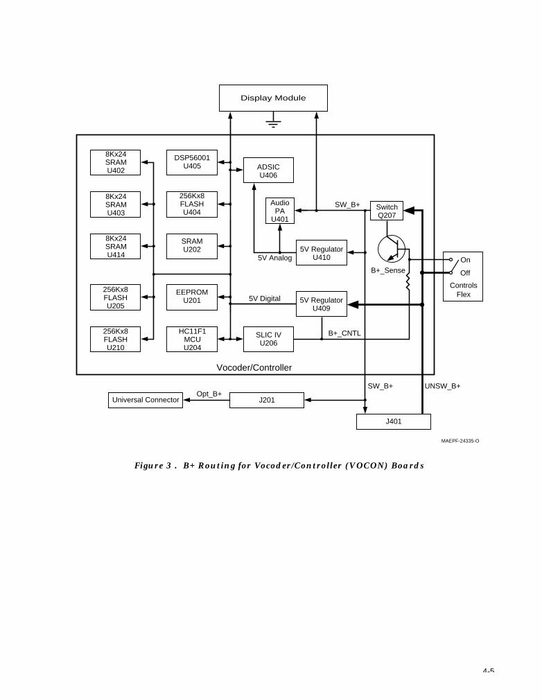
4-5
Figure 3 . B+ Routing for Vocoder/Controller (VOCON) Boards
5V RegulatorU410
ADSICU406
DSP56001U405
256Kx8FLASHU404
8Kx24SRAMU402
AudioPA
U401
SRAMU202
EEPROMU201
SLIC IVU206
SwitchQ207
On
Off
ControlsFlex
SW_B+
5V Analog
5V Digital
B+_CNTL
B+_Sense
Vocoder/Controller
UNSW_B+SW_B+
J401
J201Universal ConnectorOpt_B+
Display Module
8Kx24SRAMU403
8Kx24SRAMU414
256Kx8FLASHU205
256Kx8FLASHU210
5V RegulatorU409
MAEPF-24335-O
HC11F1MCUU204

4-6
Notes

5-1
VHF/UHF Transceiver Board Detailed Theory of Operation 5Introduction This section of the manual provides a detailed circuit description of an
ASTRO Digital SABER VHF and UHF Transceiver Board. When reading the theory of operation, refer to your appropriate schematic and component location diagrams located in the back section of this manual. This detailed theory of operation will help isolate the problem to a particular component. However, first use the ASTRO Digital SABER Portable Radios Basic Service Manual to troubleshoot the problem to a particular board.
Frequency Generation Unit (FGU)
The frequency generation unit (FGU) consists of three major sections: the high stability reference oscillator (U203), the fractional-N synthesizer (U204,) and the VCO buffer (U201). A 5V regulator (U202), supplies power to the FGU. The synthesizer receives the 5V REG at U204, and applies it to a filtering circuit within the module and capacitor C253. The well-filtered 5-volt output at U204 pin 19 is distributed to the TX and RX VCOs and the VCO buffer IC. The mixer LO injection signal and transmit frequency are generated by the RX VCO and TX VCO respectively. The RX VCO uses an external active device (Q202), whereas the VHF TX VCO active device is a transistor inside the VCO buffer. The UHF TX VCO uses two active devices, one external (Q203) and the other internal to the VCO buffer. The base and emitter connections of this internal transistor are pins 11 and 12 of U201.
The RX VCO is a Colpitts-type oscillator, with capacitors C235 and C236 providing feedback. The RX VCO transistor (Q202) is turned on when pin 38 of U204 switches from high to low. The RX VCO signal is received by the VCO buffer at U201 pin 9, where it is amplified by a buffer inside the IC. The amplified signal at pin 2 is routed through a low-pass filter (L201 and associated capacitors) and injected as the first LO signal into the mixer (U2 pin 8). In the VCO buffer, the RX VCO signal (or the TX VCO signal during transmit) is also routed to an internal prescaler buffer. The buffered output at U201 pin 16 is applied to a low-pass filter (L205 and associated capacitors). After filtering, the signal is routed to a prescaler divider in the synthesizer at U204 pin 21.
The divide ratios for the prescaler circuits are determined from information stored in a codeplug, which is part of the microcontrol unit (U204 on the VOCON board). The microprocessor extracts data for the division ratio as determined by the position of the channel-select switch (S902), and busses the signal to a comparator in the synthesizer. A 16.8MHz reference oscillator, U203, applies the 16.8MHz signal to the synthesizer at U204 pin 14. The oscillator signal

5-2
is divided into one of three pre-determined frequencies. A time-based algorithm is used to generate the fractional-N ratio.
If the two frequencies in the synthesizer’s comparator differ, a control (error) voltage is produced. The phase detector error voltage (V control) at pin 31 and 33 of U204, is applied to the loop filter consisting of resistors R211, R212, and R213, and capacitors C244, C246, C247 and C275. The filtered voltage alters the VCO frequency until the correct frequency is synthesized. The phase detector gain is set by components connected to U204 pins 28 and 29.
In the TX mode, U204 pin 38 goes high and U201 pin 14 goes low, which turns off transistor Q202 and turns on the internal TX VCO transistor in U204 and the external TX VCO buffer Q203 on the UHF circuit. The TX VCO feedback capacitors are C219 and C220. Varactor diode CR203 sets the TX frequency while varactor CR202 is the TX modulation varactor. The modulation of the carrier is achieved by using a 2-port modulation technique. The modulation of low frequency tones such as DPL/TPL is achieved by injecting the tones into the A/D section of the fractional-N synthesizer. The digitized signal is modulated by the fractional-N divider, generating the required deviation. Modulation of the high frequency audio signals is achieved by modulating the varactor (CR203) through a frequency compensation network. Resistors R207 and R208 form a potential divider for the higher frequency audio signals.
In order to cover the very wide bandwidths, positive and negative V-control voltages are used. High control voltages are achieved using positive and negative multipliers. The positive voltage multiplier circuit consists of components CR204, C256, C257 and reservoir capacitor C258.The negative multiplier circuit consists of components CR205, CR206, C266, C267 and reservoir capacitor C254 in VHF and UHF radios. Out-of-phase clocks for the positive multiplier appear at U204 pins 9 and 10. Out-of-phase clocks for the negative multiplier appear at U204 pins 7 and 8, and only when the negative V-control is required (i.e., when the VCO frequency exceeds the crossover frequency). When the negative V-control is not required, transistor Q201 is turned on, and capacitor C259 discharges. The 13V supply generated by the positive multiplier is used to power-up the phase detector circuitry. The negative V-control is applied to the anodes of the VCO varactors.
The TX VCO signal is amplified by an internal buffer in U201, routed through a low pass filter and routed to the TX PA module, U105 pin 1. The TX and RX VCOs and buffers are activated via a control signal from U204 pin 38.
The reference oscillator supplies a 16.8MHz clock to the synthesizer where it is divided down to a 2.1MHz clock. This divided-down clock is fed to the ABACUS IC (U401), where it is further processed for internal use.

5-3
Antenna Switch Two antenna switches are part of the radio circuitry. One of the switches which is located in the radio casting is mechanical. It switches between the radio antenna and a remote antenna. Switching is accomplished by a plunger located on the accessory connector. With a remote antenna installed, continuity between the radio antenna and the RF input line is broken; continuity is made from the remote antenna to the radio RF line. The second switch is a current device. It is a pair of diodes (CR108/CR109) that electronically steer RF between the receiver and the transmitter. In the transmit mode, RF is routed through transmit switching diode CR108, and sent to the antenna. In the receive mode, RF is received from the antenna, routed through receive switching diode CR109, and applied to the RF amplifier, U1 (UHF), Q1 (VHF). In transmit, bias current, sourced from U101 pin 21, is routed through L105, U104, CR108, and L122 in VHF and L105, CR108, and L122 in UHF. Sinking of the bias current is through the transmit ALC module, U101 pin 19. In the receive mode, bias current, sourced from SB+, is routed through Q107 (pin 3 to pin 2), L123 (UHF), L121, CR109, and L122. Sinking of the bias current is through the 5-volt regulator, U106 pin 8.
Receiver Front End The RF signal is received by the antenna and coupled through the external RF switch. The UHF board applies the RF signal to a low-pass filter comprised of: L126, L127, L128, C149, C150, and C151. The VHF board bypasses the lowpass filter. The filtered RF signal is passed through the antenna switch (CR109) and applied to a bandpass filter comprised of: VHF; L11 through L14, CR1 through CR9, C4, C2, and C3, or UHF; L30, L31, L32, L34, L35, CR6 through CR9, C1, C2, and C3. The bandpass filter is tuned by applying a control voltage to the varactor diodes in the filter. (CR1-CR9 in VHF and CR6-CR9 in UHF.)
The bandpass filter is electronically tuned by the D/A IC (U102) which is controlled by the microcomputer.The D/A output range is extended through the use of a current mirror, transistor Q108 and associated resistors R115 and R116. When Q108 is turned on via R115, the D/A output is reduced due to the voltage drop across R116. Depending on the carrier frequency the microcomputer will turn on or off Q108. Wideband operation of the filter is achieved by retuning the bandpass filter across the band.
The output of the bandpass filter is applied to a wideband GaAs RF amplifier IC, U1 (RF AMP) on the UHF transceiver board. The VHF board uses an active device for RF amplification (Q1). After being amplified by the RF AMP, the RF signal is further filtered by a second broad-band, fixed-tuned, bandpass filter consisting of C6, C7, C8, C80, C86, C87, C88, C97, C99, L3, L4, L5, and L30 (VHF); or C4 through C7, C88 through C94, C99, and L11 through L15 (UHF) to improve the spurious rejection.
Via a broadband 50-ohm transformer, T1, the filtered RF signal is routed to the input of a broadband mixer/buffer (U2). Mixer U2 uses GaAs FETs, in a double-balanced Gilbert Cell configuration. The RF signal is applied to the mixer at U2 pins 1 and 15. An injection signal (1st LO) of about -10dBm, supplied by the FGU, is applied to U2 pin 8. Mixing of the RF and the 1st LO results in an output signal which is

5-4
the first IF frequency. The first IF frequency of VHF and UHF bands are 45.15MHz and 73.35MHz respectively. The 1st LO signal for VHF is 45.15MHz higher than the carrier frequency while that for the UHF is 73.35MHz lower than the carrier frequency. The 1st IF signal output, at U2 pins 4 and 6, is routed through transformer T2 and impedance matching components, and applied to a 2-pole crystal filter (FL1), which is the final stage of the receiver front end. The 2-pole crystal filter removes unwanted mixer products. Impedance matching between the output of the transformer (T2) and the input of the filter (FL1) is accomplished by capacitor C605 and inductor L605 (VHF); or C611, C614 and L605 (UHF).
Receiver Back End The output of crystal filter FL1 is matched to the input of IF buffer amplifier transistor Q601 by components C610 and L604 (VHF) and C609, C610, and L600 (UHF). Transistor Q601 is biased by the 5V regulator (U202). The IF frequency on the collector of Q601 is applied to a second crystal filter through a matching circuit. The second crystal filter (FL2) input is matched by C604, C603, and L601 (VHF); or C604, L601, and L602 (UHF). The filter supplies further attenuation at the IF sidebands to increase the radios selectivity. The output of FL2 routed to pin 32 of U401 through a matching circuit which consists of L603, L606, and C608 (VHF); or L603, C606, and C605 (UHF).
In the ABACUS IC, (U401) the first IF frequency is amplified and then down converted to 450kHz, the second IF frequency. At this point, the analog signal is converted into two digital bit streams via a sigma-delta A/D converter. The bit streams are then digitally filtered and mixed down to baseband and filtered again. The differential output data stream is then sent to the ADSIC (U406) on the VOCON board where it is decoded to produce the recovered audio.
The ABACUS IC (U401) is electronically programmable, and the amount of filtering which is dependent on the radio channel spacing and signal type is controlled by the microcomputer. Additional filtering, which used to be provided externally by a conventional ceramic filter, is replaced by internal digital filters in the ABACUS IC. The ABACUS IC contains a feedback AGC circuit to expand the dynamic range of the sigma-delta converter. The differential output data contains the quadrature (I and Q) information in 16-bit words, the AGC information in a 9-bit word, imbedded word sync information and fill bits dependent on sampling speed. A fractional-n synthesizer is also incorporated on the ABACUS IC for 2nd LO generation.
The 2nd LO/VCO is a Colpitts oscillator built around transistor Q401 (VHF) and Q1 (UHF). The VCO has a varactor diode, VR401 (VHF) and CR5 (UHF), to adjust the VCO frequency. The control signal for the varactor is derived from a loop filter consisting of C426, C428, and R413.

5-5
Transmitter The transmitter consists of three major sections:
• Harmonic Filter• RF Power Amplifier Module• ALC Circuits
Harmonic Filter RF from the power amplifier (PA) module (U105) is routed through the coupler (U104), passed through the transmit antenna switch (CR108), and applied to a harmonic filtering network in UHF. In the case of a VHF transceiver board, RF from the PA module (U105) is routed also through the coupler (U104), then through the harmonic filtering network, and on to the antenna switch (CR108). The harmonic filtering circuit is comprised of the following components: L126, L127, L128, C149, C150, and C151 (for VHF models); or L126, L127, L128, C149, C150, and C151 (for UHF models). Resistor R128 (UHF) or R117 (VHF) provides a current limited 5V to J2 for mobile ASTRO vehicular adapter (AVA) applications.
RF Power Amplifier Module
The RF power amplifier module (U105) is a wide-band multi-stage amplifier (3 stages for the VHF models and 4 stages for the UHF models). Nominal input and output impedance of U105 is 50 ohms. The dc bias for U105 is on pins 2, 4, 5. In the transmit mode, the voltage on U105 pins 2 and 4 (close to the B+ level) is obtained via switching transistor Q101. Transistor Q101 receives its control base signal as follows:
• the microcomputer keys the D/A IC to produce a ready signal at U102 pin 3
• the ready signal at U102 pin 3 is applied to the TX ALC IC at U101 pin 14 (5V)
• the synthesizer sends a LOC signal to the TX ALC IC (U204 pin 40 to U101 pin 16)
When the LOC signal and the ready signal are both received, the TX ALC IC (pin 13) sends a control signal to turn on transistor Q101.
ALC Circuits Coupler module U104 samples the forward power and the reverse power of the PA output voltage. Reverse power is present when there is other than 50 ohms impedance at the antenna port. Sampling is achieved by coupling some of the forward and/or reverse power, and apply it to CR102(VHF) or CR101(UHF) and CR103 for rectification and summing. The resultant dc signal is then applied to the TX ALC IC (U101 pin 2) as RFDET to be used as an RF strength indicator.
The transmit ALC circuit, built around U101, is the heart of the power control loop. Circuits in the TX ALC module compare the signals at U101 pins 2 and 7. The resultant signal, C BIAS, at U101 pin 4 is applied to the base of transistor Q110. In response to the base drive, transistor Q110 varies the dc control voltages applied to the RF PA at U105 pin 3, thus controlling the RF power of module (U105).
Thermistor RT101 senses the temperature of the TX ALC IC. If an abnormal operating condition exists, which causes the PA slab temperature to rise to an unacceptable level, the thermistor forces the ALC to reduce the set power.

5-6
Notes

6-1
800MHz Transceiver Board Detailed Theory of Operation 6Introduction This section of the manual provides a detailed circuit description of an
ASTRO Digital SABER 800MHz Transceiver Board. When reading the theory of operation, refer to your appropriate schematic and component location diagrams located in the back section of this manual. This detailed theory of operation will help isolate the problem to a particular component. However, first use the ASTRO Digital SABER Portable Radios Basic Service Manual to troubleshooting the problem to a particular board.
Frequency Synthesis The complete synthesizer subsystem consists of the reference oscillator (U304), the voltage controlled oscillator (VCO), U307, a buffer IC (U303), and the synthesizer (U302).
The reference oscillator contains a temperature-compensated 16.8MHz crystal. This oscillator is digitally tuned and contains a temperature-referenced 5-bit analog-to-digital (A/D) converter. The output of the oscillator (pin 10 on U304) is applied to pin 14 (XTAL1) on U302 via capacitor C309 and resistor R306.
Module U307 is the voltage controlled oscillator, which is varactor tuned. That is, as the voltage (2-11V) being applied to pins 1 and 7 of the VCO varies, so does the varactor’s capacitance, thereby changing the VCO’s output frequency. The 800MHz VCO is a dual-range oscillator that covers the 806-825MHz and the 851-870MHz frequency bands. The low-band VCO (777-825MHz) provides the first LO injection frequencies (777-797MHz) that will be 73.35MHz below the carrier frequency. In addition, when the radio is operated through a repeater, the low-band VCO will generate the transmit frequencies (806-825MHz) that will be 45MHz below the receiver frequencies. The low-band VCO is selected by pulling pin 3 high and pin 8 low on U307. When radio-to-radio or talk-around operation is necessary, the high band VCO (851-870MHz) is selected. This is accomplished by pulling pin 3 low and pin 8 high on U307.
The buffer IC (U303) includes a TX, RX, and prescaler buffer whose main purpose is to individually maintain a constant output and provide isolation.The TX buffer is chosen by setting pin 7 of U303 high; the RX buffer is chosen by setting pin 7 of U303 low. The prescaler buffer will always be on. In order to select the proper combination of VCO and buffer, the following conditions must be true at pin 6 of U303 (or pin 38 of U302) and pin 7 of U303 (or pin 39 of U302). For the first LO injection frequencies 777-797MHz, pins 6 and 7 must both be low; for the TX repeater frequencies 806-825MHz pins

6-2
6 and 7 must both be high. For talkaround TX frequencies 851-870MHz, pin 6 must be low while pin 7 must be high.
The synthesizer IC (U303) consists of a prescaler, a programmable loop divider, a divider control logic, a phase detector, a charge pump, an A/D converter for low-frequency digital modulation, a balance attenuator to balance the high frequency analog modulation to the low frequency digital modulation, a 13V positive-voltage multiplier, a serial interface for control, and finally a filter for the regulated five volts. This filtered five volts is present at pin 19 of U302, pin 9 of U307, and pins 2, 3, 4, and 15 of U303. It is also applied directly to resistors R309, R315, and R311. Additionally, the 13V, being generated by the positive voltage multiplier circuitry, should be present at pin 35 of U302. The serial interface (SRL) is connected to the microprocessor via the data line (pin 2 of U302), clock line (pin 3 of U302), and chip enable line (pin 4 of U302).
The complete synthesizer subsystem works as follows. The output of the VCO, pin 4 on U307, is fed into the RF input port (pin 9) of U303. In the TX mode, the RF signal will be present at pin 4 of U303. On the other hand, in the RX mode, the RF signal will be present at pin 3 of U303. The output of the prescaler buffer, pin 15 on U303, is applied to the PREIN port (pin 21) of U302. The prescaler in U302 is a dual-modulus type with selectable divider ratios. This divider ratio is controlled by the loop divider, which in turn receives its inputs via the SRL. The loop divider adds or subtracts phase to the prescaler divider by changing the divide ratio via the modulus control line. The output of the prescaler is then applied to the loop divider. The output of the loop divider is then applied to the phase detector. The phase detector will then compare the loop divider’s output signal with the signal from U304 (that is divided down after it is applied to pin 14 of U302). The result of the signal comparison is a pulsed dc signal which is applied to the charge pump. The charge pump outputs a current that will be present at pin 32 of U302. The loop filter (which consists of capacitors C322, C317, C318, C329, C324, and C315, and resistors R307, R305, and R314) will transform this current into a voltage that will be applied to pins 1 and 7 of U307, and alter the VCO’s output frequency.
In order to modulate the PLL, the two-port modulation method is utilized. The analog modulating signal is applied to the A/D converter as well as the balance attenuator, via U302 pin 5. The A/D converter converts the low-frequency analog modulating signal into a digital code that is applied to the loop divider, thereby causing the carrier to deviate. The balance attenuator is used to adjust the VCO’s deviation sensitivity to high-frequency modulating signals.
Antenna Switch Switching between the standard and external antenna ports is accomplished with the external mechanical switch which is actuated by a plunger located on the accessory connector.
An electronic PIN diode switch steers RF between the receiver and transmitter. The common node of the switch is at capacitor C101. In the transmit mode, RF is routed to the anode of diode CR104. In receive mode, RF is routed to pin 1 of U201. In transmit, bias current sourced from U504 pin 21, is routed through PIN diodes CR104 and

6-3
CR102, biasing them to a low-impedance state. Bias current returns to ground through U504 pin 20. In receive, U504 pin 21 is pulled down to ground and pin 20 is pulled up to B+, reverse biasing diodes CR104 and CR102 to a high impedance.
Receiver Front End For the purposes of this discussion, the receiver front end is defined to be the circuitry from the antenna switch to the output of the IF crystal filter. The 800MHz front end is designed to convert the received RF signal to the 1st IF frequency of 73.35MHz, while at the same time providing for spurious immunity and adjacent channel selectivity. A review of the interstage components of the front end will now be presented with emphasis on troubleshooting considerations.
The received RF signal is passed through the antenna switch input matching components C101, L105, and C114 tank components C106 and L103 (which are anti-resonant at the radios transmitter frequencies), and output matching components C103 and L104. Both pin diodes CR102 and CR104 must be back biased to properly route the received signal.
The stage following the antenna switch is a 50-ohm, inter-digitated, 3-pole, stripline preselector (U201). The preselector is positioned after the antenna switch to provide the receiver preamp some protection to strong signal, out-of-band signals.
After the preselector (U201), the received signal is processed through the receiver preamp, U202. The preamp is a dual-gate GaAs MESFET transistor which has been internally biased for optimum IM, NF, and gain performance. Components L201 and L202 match the input (gate 1) of the amp to the first preselector, while at the same time connecting gate 1 to ground potential. The output (drain) of the amp is pin 3 and is matched to the subsequent receiver stage via components L204, C205 and C222. A supply voltage of 5Vdc is provided to pin 3 via an RF choke L203 and bypass C204. The 5 volt supply is also present at pin 4 which connects to a voltage divider network that biases gate 2 (pin 5) to a predefined quiescent voltage of 1.2Vdc. Resistor R202 and capacitor C203 are connected to pin 5 to provide amp stability. The FET source (pin 7) is internally biased at 0.55 to 0.7Vdc for proper operation with bypass capacitors C201 and C202 connected to the same node.
The output of the amp is matched to a second 3-pole preselector (U203) of the type previously discussed. The subsequent stage in the receiver chain is the 1st mixer U205, which uses low-side injection to convert the RF carrier to an intermediate frequency (IF) of 73.35MHz. Since low-side injection is used, the LO frequency is offset below the RF carrier by 73.35MHz, or Flo = Frf - 73.35MHz. The mixer utilizes GaAs FETs in a double balanced Gilbert Cell configuration. The LO port (pin 8) incorporates an internal buffer and a phase shift network to eliminate the need for a LO transformer. The LO buffer bypass capacitors (C208, C221, and C216) are connected to pin 10 of U205, and should exhibit a nominal dc voltage of 1.2 to 1.4Vdc. Pin 11 of U205 is LO buffer Vdd (5Vdc) with associated bypass capacitors C226 and C209 connected to the same node. An internal voltage divider network within the LO buffer is bypassed to virtual ground at pin 12

6-4
of U205 via bypass C213. The mixer’s LO port is matched to the radio’s PLL by a capacitive tap, C207 and C206. A balun transformer (T202) is used to couple the RF signal into the mixer. The primary of T202 is matched to the preceding stage by capacitor C223, with C227 providing a dc block to ground. The secondary of T202 provides a differential output, with a 180° phase differential being achieved by setting the secondary center tap to virtual ground using bypass capacitors C210, C211 and C212. The secondary of transformer T202 is connected to pins 1 and 15 of the mixer IC, which drives the source leg of dual FETs used to toggle the paralleled differential amplifier configuration within the Gilbert Cell.
The final stage in the receiver front end is a 2-pole crystal filter (FL1). The crystal filter provides some of the receiver’s adjacent channel selectivity. The input to the crystal filter is matched to the 1st mixer using components L605, C611 and C614. The output of the crystal filter is matched to the input of IF buffer amplifier transistor Q601 by components L600, C609, and C610.
Receiver Back End The IF frequency on the collector of Q601 is applied to a second crystal filter (FL2) through a matching circuit consisting of L601, L602, C604, and C612. The filter supplies further attenuation at the IF sidebands to increase the radio’s selectivity. The output of FL2 is routed to pin 32 of U401 through a matching circuit which consists of L603, C605, and C606 and dc block capacitor C613.
In the ABACUS IC, (U401) the first IF frequency is amplified and then down converted to 450kHz, the second IF frequency. At this point, the analog signal is converted into two digital bit streams via a sigma-delta A/D converter. The bit streams are then digitally filtered and mixed down to baseband and filtered again. The differential output data stream is then sent to the ADSIC (U406) on the VOCON board where it is decoded to produce the recovered audio.
The ABACUS IC (U401) is electronically programmable, and the amount of filtering which is dependent on the radio channel spacing and signal type is controlled by the microcomputer. Additional filtering, which used to be provided externally by a conventional ceramic filter, is replaced by internal digital filters in the ABACUS IC. The ABACUS IC contains a feedback AGC circuit to expand the dynamic range of the sigma-delta converter. The differential output data contains the quadrature (I and Q) information in 16-bit words, the AGC information in a 9-bit word, imbedded word sync information and fill bits dependent on sampling speed. A fractional-n synthesizer is also incorporated on the ABACUS IC for 2nd LO generation.
The second LO/VCO is a Colpitts oscillator built around transistor Q1. The VCO has a varactor diode (VR401), which is used to the adjust the VCO frequency. The control signal for the varactor is derived from a loop filter consisting of C426, C428, and R413.

6-5
Transmitter The 800MHz RF power amplifier (PA) is a 5-stage amplifier (U502). The RF power amplifier has a nominal input and output impedance of 50 ohms.
An RF input drive level of approximately +3dBm, supplied from the VCO buffer IC (U303), is applied to pin 1 of U502. The dc bias for the internal stages of U502 is applied to pins 2, 5, and 6 of the module. Pins 2 and 5 being switched through Q502 and pin 6 being unswitched B+ to the final amplifier stage. Power control is achieved through the varying of the dc bias to pins 3 and 4, the third and fourth amplifier stages of the module. The amplified RF signal leaves the PA module via pin 7 and is applied to the directional coupler (U501).
The purpose of U501 is to sample both the forward power and the reverse power. The reverse power will be present when there is other than a 50-ohm load at the antenna port. The sampling will be achieved by coupling some of the reflected power, forward and/or reverse, to a coupled leg on the coupler. The sampled RF signals are applied to diode CR501 for rectification and summing. The resultant dc signal is applied to the ALC IC (U504 pin 2) as RFDET to be used as an strength indicator of the RF signal being passed through the directional coupler (U501).
The transmit ALC IC (U504) is the heart of the power control loop. The REF V line (U504 pin 7), a dc signal supplied from the D/A IC (U503), and the RF DET signal described earlier, are compared internally in the ALC IC to determine the amount of C BIAS, pin 4, to be applied to the base of transistor Q501. Transistor Q501 responds to the base drive level by varying the dc control voltages applied to pin 3 and 4 of the RF PA, controlling the RF power level of module, U502. The ALC IC also controls the base switching to transistor Q502 via pin 12, BIAS.
The D/A IC (U503) controls the dc switching of the transceiver board. Its outputs, SC1 and SC3, pins 12 and 14 respectively, control transistor Q503, which then supplies TX 5V and RX 5V to the transceiver board. The D/A also supplies the dc bias to the detector diode (CR501) via pin 7, and the REF V signal to the ALC IC (U504).

6-6
Notes

7-1
VOCON Board Detailed Theory of Operation 7Introduction This section of the manual provides a detailed circuit description of an
ASTRO Digital SABER VOCON (Vocoder/Controller) Board. When reading the theory of operation, refer to your appropriate schematic and component location diagrams located in the back section of this manual. This detailed theory of operation will help isolate the problem to a particular component. However, first use the ASTRO Digital SABER Portable Radios Basic Service Manual to troubleshooting the problem to a particular board.
General The VOCON board consists of two subsystems:
• vocoder
• controller
Although these two subsystems share the same printed circuit board and work closely together, it helps to keep their individual functionality separate in describing the operation of the radio.
The controller section is the central interface between the various subsystems of the radio. It is very similar to the digital logic portion of the controllers on many existing Motorola radios. Its main task is to interpret user input, provide user feedback, and schedule events in the radio operation, which includes programming ICs, steering the activities of the DSP and driving the display.
The vocoder section performs the functions which previously were performed by analog circuitry. This includes all tone signaling, trunking signalling, and conventional analog voice, etc. All analog signal processing is done digitally utilizing a DSP56001. In addition it provides a digital voice plus data capability utilizing VSELP or IMBE voice compression algorithms. Vocoder is a general term used to refer to these DSP based systems and is short for voice encoder.
In addition, the VOCON board provides the interconnect between the microcontrol unit (MCU), DSP, and the encryption board on secure-equipped radios.

7-2
Controller Section Refer to Figure 4 and your specific schematic diagram.
The controller section of the VOCON board consists entirely of digital logic comprised of a microcontrol unit (MCU-U204), a custom support logic IC (SLIC-U206), and memory consisting of: SRAM (U202), EEPROM (U201), and FLASH memory (U205, U210).
The MCU (U204) memory system is comprised of a 32k x 8 SRAM (U202), 32k x 8 EEPROM (U201), and 512k x 8 FLASH ROM (U205,U210). The MCU also contains 1024 bytes of internal SRAM and 512 bytes of internal EEPROM. The EEPROM memory is used to store customer specific information and radio personality features. The FLASH ROM contains the programs which the HC11F1 executes. The FLASH ROM allows the controller firmware to be reprogrammed for future software upgrades or feature enhancements. The SRAM is used for scratchpad memory during program execution.
The SLIC (U206) performs many functions as a companion IC for the MCU. Among these are expanded input/output (I/O), memory decoding and management, and interrupt control. It also contains the universal asynchronous receiver transmitter (UART) used for the RS232 data communications. The SLIC control registers are mapped into the MCU (U204) memory space.
Figure 4 . VOCON Board - Controller Section
U205256Kx8FLASH
U210256Kx8FLASH
U20232Kx8SRAM
U20132Kx8
EEPROM
Address/Data/Control
Resets Clocks
Controls
Chip Selects/Bank Control
GeneralPurpose I/O
RS232
U206SLIC IV
SPI
SCI
A/D
Address/Data/Control
Clocks
GeneralPurpose I/O
512 BytesEEPROM
1024 BytesSRAM
U204MC68HC11F1
HC11/DSPInterface
Universal Connector
Universal Connector
Transceiver/Display
MAEPF-24337-O
ADSIC

7-3
The controller performs the programming of all peripheral ICs. This is done through a serial peripheral interface (SPI) bus. ICs programmed through this bus include the synthesizer, DAIC, reference oscillator, display, and ADSIC. On secure-equipped model, the encryption board is also controlled through the SPI bus.
In addition to the SPI bus, the controller also maintains two asynchronous serial busses; the SB9600 bus and an RS232 serial bus. The SB9600 bus is for interfacing the controller section to different hardware option boards, some of which may be external to the radio. The RS232 is used for the function of a common data interface for external devices.
User input is handled by the controller through top rotary controls and side buttons. On models with a display, an additional 3 x 2 or 3 x 6 keypad are also read. User feedback is provided by a single bicolor LED on the top and a two-line, fourteen-character display if equipped.
The controller schedules the activities of the DSP through the host port interface. This includes setting the operational modes and parameters of the DSP. The controlling of the DSP is analogous to programming analog signaling ICs on standard analog radios.
Vocoder Section Refer to Figure 5 and your specific schematic diagram.
The vocoder section of the VOCON board is made up of a digital signal processor (DSP-U405), 24k x24 static-RAM (SRAMs-U414, U403, and U402), 256kB FLASH ROM (U404), ABACUS/DSP support IC (ADSIC-U406), and an audio PA (U401).
The FLASH ROM (U404) contains the program code executed by the DSP. As with the FLASH ROM used in the controller section, the FLASH ROM is reprogrammable so new features and algorithms can be updated in the field as they become available. Depending on the mode and operation of the DSP, corresponding program code is moved from the FLASH ROM into the faster SRAM, where it is executed at full bus rate.
The ADSIC (U406) is basically a support IC for the DSP. It provides among other things, the interface from the digital world of the DSP to the analog world. The ADSIC also provides some memory management and provides interrupt control for the DSP processing algorithms. The configuration programming of the ADSIC is performed by the MCU. However some components of the ADSIC are controlled through a parallel memory mapped register bank by the DSP.
In the receive mode, The ADSIC (U406) acts as an interface to the ABACUS IC, which can provide IF data samples directly to the DSP for processing. Or the IF data can be filtered and discriminated by the ADSIC and data provided to the DSP as raw discriminator sample data. The latter mode, with the ADSIC performing the IF filtering and discrimination, is the typical mode of operation.

7-4
In the transmit mode, the ADSIC (U406) provides a serial digital-to-analog (D/A) converter. The data generated by the DSP is filtered and reconstructed as an analog signal to present to the VCO as a modulation signal. Both the transmit and receive data paths between the DSP and ADSIC are through the DSP SSI port.
The only analog device in the vocoder section is the audio PA (U401). This IC is an audio amplifier for the microphone analog input and speaker analog output. The audio PA allows steering between the internal and external microphone and internal and external speaker. Steering is accomplished through four control lines provided by the ADSIC and controlled by the DSP through the ADSIC parallel registers.
The amplified microphone signal is provided to the ADSIC, which incorporates an analog-to-digital (A/D) converter to translate the analog waveform to a series of data. The data is available to the DSP through the ADSIC parallel registers. In the converse way, the DSP writes speaker data samples to a D/A in the ADSIC, which provides an analog speaker audio signal to the audio PA.
Figure 5 . VOCON Board - Vocoder Section
SSISERIAL
EX
TA
L
MO
DB
MO
DA
HC11/DSPInterface
D0-D23
BUSCONTROL
A0-A15
U405DSP56001 SCI
SERIALEncryptionInterface
HostPort
U401Audio PA
SystemClock
Gata ArrayLogic
ABACUS RxInterface
Tx D/A
GeneralPurpose I/O
SpeakerD/A
MicrophoneA/D
SerialConfig.
U406ADSIC ABACUS
Interface
ModulationOut
ExternalMicrophone
InternalMicrophone
ExternalSpeaker
InternalSpeaker
U4148Kx24SRAM
U404256Kx8FLASH
U4038Kx24SRAM
U4028Kx24SRAM
HC11SPI
MAEPF-24338-O

7-5
Switched Regulator All of the digital circuitry on the VOCON is supplied 5 volt regulated dc by a switched mode regulator (refer to Figure 3 on page 5 of Chapter 4). The fundamental parts of the regulator are U409, L402, C470, CR403, C463, and U407. Module U409 is a pulse width modulating (PWM) switched regulator controller. Coil L402 is an energy storage element, C470 is an output ripple filter, and CR403 is a Schottky diode switch. Capacitor C463 is added for UNSW_B+ ripple filter and is necessary for stability of the regulator. Module U407 is a supply supervisory IC, which provides a system reset function when the output of the regulator falls out of regulation, typically around 4.6Vdc.
This switched mode regulator works by supplying just sufficient energy to the storage element to maintain the output power of the regulator at 5Vdc. It can be related to a flywheel in the sense that just enough energy can be added to a spinning flywheel to keep it spinning at a constant speed. In contrast to a typical linear type regulator, which basically shunts unused current to ground through an active resistive divider. The switched mode regulator is much more energy efficient. It can be noted that input current to the regulator is less than the load current. In fact, as input voltage to the regulator goes up, current supplied to the regulator actually goes down for a constant load.
Module U409 works off of a clock with a nominal operating frequency of 160kHz (kit number NTN7749E), or 260kHz (kit numbers NTN7749F and NTN7749G). This may vary a little based on the load and input voltage. It maintains regulation by varying the duty cycle of a clock output driving L402. This signal is referred to as Lx on U409 (refer to Waveform W1). As long as the clock output is high, current flows from the supply into L402 allowing energy to be stored. When the clock output goes low, the diode CR403 conducts, allowing current to continue to flow from ground through L402. A pulse width on the Lx signal can be obtained, which provides the correct amount of energy to keep the output in regulation. Capacitor C470 is an output filter to reduce ripple on the output from the clock transitions.
Module U409 is supplied directly from the unswitched battery supply. It is turned on and off through the control line connected to SHDN*/ON/OFF. This is the same control line from the MCU, which controls the series pass element Q207, which switches SW_B+. A voltage level of approximately 2Vdc is required to turn the regulator on.

7-6
RX Signal Path The vocoder processes all received signals digitally. This requires a unique back end from a standard analog radio. This unique functionality is provided by the ABACUS IC with the ADSIC (U406) acting as the interface to the DSP. The ABACUS IC located on the transceiver board provides a digital back end for the receiver section. It provides a digital output of I (In phase) and Q (Quadrature) data words which represent the IF (Intermediate Frequency) signal at the receiver back end (refer to appropriate transceiver section for more details on ABACUS operation). This data is passed to the DSP through an interface with the ADSIC (U406) for appropriate processing.
The ADSIC interface to the ABACUS is comprised of the four signals SBI, DIN, DIN*, and ODC (refer to Figure 6).
NOTE: An asterisk symbol (*) next to a signalname indicates a negative or NOT logictrue signal.
ODC is a clock ABACUS provides to the ADSIC. Most internal ADSIC functions are clocked by this ODC signal at a rate of 2.4MHz and is available as soon as power is supplied to the circuitry. This signal may initially be 2.4 or 4.8MHz after power-up. It is programmed by the ADSIC through the SBI signal to 2.4MHz when the ADSIC is initialized by the MCU through the SPI bus. For any functionality of the ADSIC to exist, including initial programming, this reference clock must be present. SBI is a programming data line for the ABACUS. This line is used to configure the operation of the ABACUS and is driven by the ADSIC. The MCU programs many of the ADSIC operational features through the SPI interface. There are 36 configuration registers in the ADSIC of which four contain configuration data for the ABACUS. When these particular registers are programmed by the MCU, the ADSIC in turn sends this data to the ABACUS through the SBI.
Figure 6 . DSP RSSI Port - RX Mode
48KHz TX Data Interrupt
Serial Transmit Data
Serial Receive Data
2.4 MHz Receive Data Clock
20 KHz RX Data Interrupt
1.2 MHz Tx Data Serial Clock
D8-D23
A0-A2,A13-A15,RD*,WR*
SCKR
RFS
TFS
SCKT
RXD
TXD
ADSICU406
GCB0-GCB3
ToAudio PA
U401
SDO
SC0
SC1
SC2
SCK
SRD
STD
SSISERIAL
DSP56001U405
IRQB IRQB8KHz
SBI
DIN
DIN-
IDCODC
Data In
Data In*
SBI
ABACUS IIInterface
J401-1
J401-2
J401-8
J401-4
MAEPF-24339-O

7-7
DIN and DIN* are the data lines in which the I and Q data words are transferred from the ABACUS. These signals make up a deferentially encoded current loop. Instead of sending TTL type voltage signals, the data is transferred by flowing current one way or the other through the loop. This helps reduce internally generated spurious emissions on the transceiver board. The ADSIC contains an internal current loop decoder which translates these signals back to TTL logic and stores the data in internal registers.
In the fundamental mode of operation, the ADSIC transfers raw IF data to the DSP. The DSP can perform IF filtering and discriminator functions on this data to obtain a baseband demodulated signal. However, the ADSIC contains a digital IF and discriminator function and can provide this baseband demodulated signal directly to the DSP, this being the typical mode of operation. The internal digital IF filter is programmable up to 24 taps. These taps are programmed by the MCU through the SPI interface.
The DSP accesses this data through its SSI serial port. This is a 6 port synchronous serial bus. It is actually used by the DSP for both transmit and receive data transferal, but only the receive functions will be discussed here. The ADSIC transfers the data to the DSP on the SRD line at a rate of 2.4MHz. This is clocked synchronously by the ADSIC which provides a 2.4MHz clock on SC0. In addition, a 20kHz interrupt is provided on SC1 signaling the arrival of a data packet. This means a new I and Q sample data packet is available to the DSP at a 20kHz rate which represents the sampling rate of the received data. The DSP then processes this data to extract audio, signaling, etc. based on the 20kHz interrupt.
In addition to the SPI programming bus, the ADSIC also contains a parallel configuration bus consisting of D8-D23, A0-A2, A13-A15, RD*, and WR*, This bus is used to access registers mapped into the DSP memory starting at Y:FFF0. Some of these registers are used for additional ADSIC configuration controlled directly by the DSP. Some of the registers are data registers for the speaker D/A. Analog speaker audio is processed through this parallel bus where the DSP outputs the speaker audio digital data words to this speaker D/A and an analog waveform is generated which is output on SDO (Speaker Data Out). In conjunction with the speaker D/A, the ADSIC contains a programmable attenuator to set the rough signal attenuation. However, the fine levels and differences between signal types is adjusted through the DSP software algorithms. The speaker D/A attenuator setting is programmed by the MCU through the SPI bus.
The ADSIC provides an 8kHz interrupt to the DSP on IRQB for processing the speaker data samples. IRQB is also one of the DSP mode configuration pins at start up. This 8kHz signal must be enabled through the SPI programming bus by the MCU and is necessary for any audio processing to occur.
For secure messages, the analog signal data may be passed to the secure module prior to processing speaker data for decryption. The DSP transfers the data to and from the secure module through it's SCI port consisting of TXD and RXD. The SCI port is a two wire duplex asynchronous serial port. Configuration and mode control of the secure module is performed by the MCU through the SPI bus.
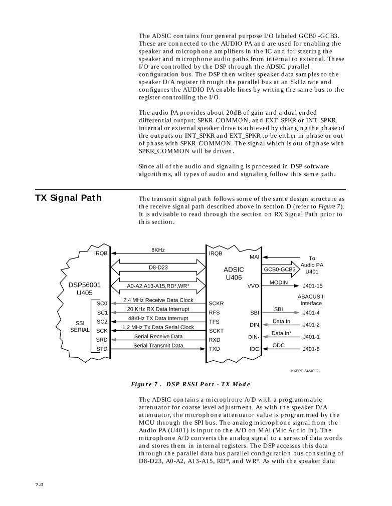
7-8
The ADSIC contains four general purpose I/O labeled GCB0 -GCB3. These are connected to the AUDIO PA and are used for enabling the speaker and microphone amplifiers in the IC and for steering the speaker and microphone audio paths from internal to external. These I/O are controlled by the DSP through the ADSIC parallel configuration bus. The DSP then writes speaker data samples to the speaker D/A register through the parallel bus at an 8kHz rate and configures the AUDIO PA enable lines by writing the same bus to the register controlling the I/O.
The audio PA provides about 20dB of gain and a dual ended differential output; SPKR_COMMON, and EXT_SPKR or INT_SPKR. Internal or external speaker drive is achieved by changing the phase of the outputs on INT_SPKR and EXT_SPKR to be either in phase or out of phase with SPKR_COMMON. The signal which is out of phase with SPKR_COMMON will be driven.
Since all of the audio and signaling is processed in DSP software algorithms, all types of audio and signaling follow this same path.
TX Signal Path The transmit signal path follows some of the same design structure as the receive signal path described above in section D (refer to Figure 7). It is advisable to read through the section on RX Signal Path prior to this section.
The ADSIC contains a microphone A/D with a programmable attenuator for coarse level adjustment. As with the speaker D/A attenuator, the microphone attenuator value is programmed by the MCU through the SPI bus. The analog microphone signal from the Audio PA (U401) is input to the A/D on MAI (Mic Audio In). The microphone A/D converts the analog signal to a series of data words and stores them in internal registers. The DSP accesses this data through the parallel data bus parallel configuration bus consisting of D8-D23, A0-A2, A13-A15, RD*, and WR*. As with the speaker data
Figure 7 . DSP RSSI Port - TX Mode
48KHz TX Data Interrupt
Serial Transmit Data
Serial Receive Data
2.4 MHz Receive Data Clock
20 KHz RX Data Interrupt
1.2 MHz Tx Data Serial Clock
D8-D23
A0-A2,A13-A15,RD*,WR*
SCKR
RFS
TFS
SCKT
RXD
TXD
ADSICU406
GCB0-GCB3
ToAudio PA
U401
MAI
VVOMODIN
J401-15
SC0
SC1
SC2
SCK
SRD
STD
SSISERIAL
DSP56001U405
IRQB IRQB8KHz
SBI
DIN
DIN-
IDCODC
Data In
Data In*
SBI
ABACUS IIInterface
J401-1
J401-2
J401-8
J401-4
MAEPF-24340-O

7-9
samples, the DSP reads the microphone samples from registers mapped into it's memory space starting at Y:FFF0. The ADSIC provides an 8kHz interrupt to the DSP on IRQB for processing these microphone data samples.
As with the received trunking low speed data, low speed data is processed by the MCU and returned to the DSP at the DSP SCLK port connected to the MCU port PA0.
For secure messages, the analog signal may be passed to the secure module for encryption prior to further processing. The DSP transfers the data to and from the secure module through it's SCI port consisting of TXD and RXD. Configuration and mode control of the secure module is performed by the MCU through the SPI bus.
The DSP processes these microphone samples and generates and mixes the appropriate signaling and filters the resultant data. This data is then transferred to the ADSIC IC on the DSP SSI port. The transmit side of the SSI port consists of SC2, SCK, and STD. The DSP SSI port is a synchronous serial port. SCK is the 1.2MHz clock input derived from the ADSIC which makes it synchronous. The data is clocked over to the ADSIC on STD at a 1.2MHz rate. The ADSIC generates a 48kHz interrupt on SC2 so that a new sample data packet is transferred at a 48kHz rate and sets the transmit data sampling rate at 48Ksp. These samples are then input to a transmit D/A which converts the data to an analog waveform. This waveform is actually the modulation out signal from the ADSIC port VVO and is connected directly to the VCO. The transmit side of the transceiver is virtually identical to a standard analog FM radio.
Also required is the 2.4MHz ODC signal from the ABACUS IC. Although the ABACUS IC provides receiver functions it is important to note that this 2.4MHz reference is required for all of the ADSIC operations.

7-10
Controller Bootstrap and Asynchronous Buses
The SB9600 bus is an asynchronous serial communications bus utilizing a Motorola proprietary protocol. Its purpose is a means for the MCU to communicate with other hardware devices. In the ASTRO Digital SABER radio, it communicates with hardware accessories connected to the universal connector.
The SB9600 bus utilizes the UART internal to the MCU operating at 9600 baud. The SB9600 bus consists of a LH_DATA (J201-4) and SB9600_BUSY (J201-6) signals. LH_DATA is actually the SCI TXD and RXD ports (U204 - PD0 and PD1) tied together through the MUX U208 (see Figure 8). This makes the bus a simplex single-wire system. SB9600_BUSY (U204 - PA3) is an active low signal, which is pulled low when a device wants control of the bus.
The same UART internal to the MCU is used in the controller bootstrap mode of operation. This mode is used primarily in downloading new program code to the FLASH ROMs on the VOCON board. In this mode, the MCU accepts special code downloaded at 7200 baud through the SCI bus instead of operating from program code resident in its ROMs. It however must operate in a two wire duplex configuration.
A voltage applied to J201-13 (Vpp) of greater than 10 Vdc will trip the circuit consisting of Q203, Q204, and VR207. This circuit sets the MODA and MODB pins of the MCU to bootstrap mode (logic 0,0) and configures the MUX, U208 to separate the RXD and TXD signals of the
Figure 8 . Host SB9600 and RS232 Ports
PD1 (TXD)
PD0 (RXD)
HC11F1U204
SLIC IVU206
U208
J201-4LH_DATA/BOOT_DATA_OUT
J201-15RS232_DATA_OUT/BOOT_DATA_IN
BOOT_DATA_IN
BOOT_DATA_OUT
J201-15SB9600_BUSY
PA3
J201-10RTS_IN*
J201-8RS232_DATA_IN
J201-14CTSOUT*
RXDIN
PJ3
RTSBIN
SLIC IVU206
MAEPF-24341-O
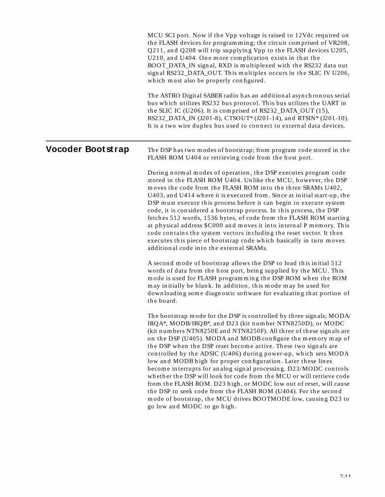
7-11
MCU SCI port. Now if the Vpp voltage is raised to 12Vdc required on the FLASH devices for programming; the circuit comprised of VR208, Q211, and Q208 will trip supplying Vpp to the FLASH devices U205, U210, and U404. One more complication exists in that the BOOT_DATA_IN signal, RXD is multiplexed with the RS232 data out signal RS232_DATA_OUT. This multiplex occurs in the SLIC IV U206, which must also be properly configured.
The ASTRO Digital SABER radio has an additional asynchronous serial bus which utilizes RS232 bus protocol. This bus utilizes the UART in the SLIC IC (U206). It is comprised of RS232_DATA_OUT (15), RS232_DATA_IN (J201-8), CTSOUT* (J201-14), and RTSIN* (J201-10). It is a two wire duplex bus used to connect to external data devices.
Vocoder Bootstrap The DSP has two modes of bootstrap; from program code stored in the FLASH ROM U404 or retrieving code from the host port.
During normal modes of operation, the DSP executes program code stored in the FLASH ROM U404. Unlike the MCU, however, the DSP moves the code from the FLASH ROM into the three SRAMs U402, U403, and U414 where it is executed from. Since at initial start-up, the DSP must execute this process before it can begin to execute system code, it is considered a bootstrap process. In this process, the DSP fetches 512 words, 1536 bytes, of code from the FLASH ROM starting at physical address $C000 and moves it into internal P memory. This code contains the system vectors including the reset vector. It then executes this piece of bootstrap code which basically in turn moves additional code into the external SRAMs.
A second mode of bootstrap allows the DSP to load this initial 512 words of data from the host port, being supplied by the MCU. This mode is used for FLASH programming the DSP ROM when the ROM may initially be blank. In addition, this mode may be used for downloading some diagnostic software for evaluating that portion of the board.
The bootstrap mode for the DSP is controlled by three signals; MODA/IRQA*, MODB/IRQB*, and D23 (kit number NTN8250D), or MODC (kit numbers NTN8250E and NTN8250F). All three of these signals are on the DSP (U405). MODA and MODB configure the memory map of the DSP when the DSP reset become active. These two signals are controlled by the ADSIC (U406) during power-up, which sets MODA low and MODB high for proper configuration. Later these lines become interrupts for analog signal processing. D23/MODC controls whether the DSP will look for code from the MCU or will retrieve code from the FLASH ROM. D23 high, or MODC low out of reset, will cause the DSP to seek code from the FLASH ROM (U404). For the second mode of bootstrap, the MCU drives BOOTMODE low, causing D23 to go low and MODC to go high.

7-12
SPI Bus Interface This bus is a synchronous serial bus made up of a data, a clock, and an individual IC unique select line. It's primary purpose is to configure the operating state of each IC. ICs programmed by this include; display module, ADSIC, Fractional N Synthesizer, Pendulum Reference Oscillator, DAIC, and if equipped, the secure module.
The MCU (U204) is configured as the master of the bus. It provides the synchronous clock (SPI_SCK), a select line, and data (MOSI [Master Out Slave In]). In general the appropriate select line is pulled low to enable the target IC and the data is clocked in. Actually the SPI bus is a duplex bus with the return data being clocked in on MISO (Master In Slave Out). The only place this is used is when communicating with the secure module. In this case, the return data is clocked back to the MCU on MISO (master in slave out).
Universal Connector and Option Selects
The universal connector is located on the back of the radio. It is the external port or interface to the outside and is used for programming and interfacing to external accessories. The signals are outlined in the following diagram. The universal connector connects to the VOCON board at J201 through a flex circuit routed down the back of the external housing. Connections to the universal connector and J201 on the VOCON board are shown in Figure 9 and Figure 10.
Figure 9 . Universal Connector
1 2 3
4 5 6
7 8 9
10 11 12
VIEW FROM BACK OFRADIO
1. Speaker Common2. External Speaker3. LH data/ Boot data out4. External MIC5. CTSOUT*6. SB9600 Busy7. Option Select 18. Opt B+/ Boot Sel/ Vpp9. RTSIN*/ Keyfail
10. Opt sel2 (Keyload)11. RS232 data out/ Boot data in12. RS232 data in
SIGNAL NAMES
MAEPF-24343-O
Figure 10 . VOCON Board Connector - J201
VOCON BOARD CONNECTOR
J201-1 N.CJ201-2 N.C.J201-3 N.C.J201-4 LH_DATA/BOOT_DATA_OUTJ201-5 Ext MicJ201-6 SB9600_BUSYJ201-7 Option Select 1J201-8 RS232_DATA_INJ201-9 Option Sel 2 (Keyload*)J201-10 RTSIN*/KEYFAIL*J201-11 Speaker CommonJ201-12 External SpeakerJ201-13 OPTB+/Boot Sel/VppJ201-14 CTSOUT*J201-15 RS232 Data Out/ Boot Data In
214
115
MAEPF-24344-O
7-13
Most of the signals are extensions of circuits described in other areas of this manual. However there are two option select pins used to configure special modes; Option Select 1 and Option Select 2. These pins are controlled by accessories connected to the universal connector. The following table outlines their functions as defined at the universal connector:
Keypad and Display Module
The front cover assembly contains the internal speaker, and internal microphone. An optional integral 2 line by 14 character LCD display is available with either a 3 x 2 keypad or 3 x 6 keypad. This unit is not considered field repairable.
The internal speaker and microphone are connected to the VOCON connector J701 through a flex circuit. This flex circuit along with J701 also contain the keypad control lines. The keypad is read though a row and column matrix made up of ROW1, ROW2, ROW3, ROW4, ROW5, ROW6, and COL1, COL2, and COL3. These signals are input to I/O ports on the SLIC (U206) and individually pulled to a high state through resistors. When a key is pressed the respective signals for a single row and a single column are set to logic zero. The MCU reads these ports through the SLIC parallel registers, provides for key debounce, and determines which key has been pressed.
The display is controlled by the MCU which programs the display through the SPI bus, DISP_EN* (select) and DISP_RST*. In addition display backlighting is provided by two white LEDs controlled by the BL_EN signal. SW_B+ routed to the display is used to power these LEDs. All other circuitry on the display is powered by 5Vdc provided by the VOCON board. The display is connected to the VOCON board at J601 through a separate flex circuit.
Table 1 . Option Select Functions
Opt Sel 1 Opt Sel 2
Keyload 1 0
No Function 1 1
External PTT 0 1

7-14
Controls and Control Top Flex
The control top controls include an on/off switch, volume, 16 position mode select switch with two position toggle, and ergo code/clear mode switch with additional emergency switch. The side controls include three momentary push button switches (monitor, RAT1, RAT2) and PTT. These components are connected through a flex circuit to the controller at J901, see Figure 11.
UNSW_B+ is routed through S901 to provide the B+_SENSE signal which provides radio power control. Refer to the power distribution section for further details.
Volume control is provides by R901 which is a potentiometer biased between +5Vdc and ground. The VOL signal is a voltage level between +5Vdc and 0Vdc dependent on the position of the rotary knob. VOL is an input to an A/D port on the MCU (U204). The MCU sends the appropriate message to the DSP to adjust speaker volume based on this setting.
Switch S903 is the two-position programmable switch typically used for code or clear mode selection. It is an input to a control I/O with a pull up resistor so the logic defaults high. Selecting clear mode pulls this signal to a logic low. Appropriate operation is configured by the MCU. In addition, this switch contains an additional momentary button typically used for emergency. This button is connected along with the PTT, and programmable side buttons on a resistor divider network biased between +5Vdc and ground. This network made up of R902, R903, and R904 provides a voltage level to an A/D port on the MCU dependent on which button is pressed. The MCU determines which button is pressed based on the value at the A/D port.
Figure 11 . Control Top Flex
R90291K
R904150K
SB1(MON)
SB2
SB3
S903 TOP BUTTON
PTT
1
248B
S902Zone/Channel
Select
C C A
R901 VOLS901ON/OFF
12345UNSW_B+ (1)
+5V (5)
PROG_SWITCH (2)
VOL (3)
EMERG (4)
B+_SENSE (10)
GREEN_LED (8)
RED_LED (12)
INT_PTT* (6)
RTA0 (11)RTA1 (13)RTA2 (15)RTA3 (7)
A/B SWITCH (9)
DGND (14)
CR901RED
CR902GREEN
123
To ControllerJ901
R90368K
MAEPF-24345-O

7-15
S902 is a binary coded switch. The output pins from this switch are connected to I/O ports on the controller. It provides a 4 bit binary word to the MCU indicating which of the 16 positions the rotary is set to. This switch provides an additional output, A/B_SWITCH, which effectively doubles its range by providing decoding for two sets of 16 positions. A/B_SWITCH is also read by the MCU on an I/O port.
Controller Memory Map
Figure 12 depicts the controller section memory map for the parallel data bus as used in normal modes of operation. There are three maps available for normal operation, but map 2 is the only one used. In bootstrap mode, the mapping is slightly different and will be addressed later.
The external bus for the host controller (U204)) consists of one 32Kx8 SRAM (U202), one 32Kx8 EEPROM (U201), two 256Kx8 FLASH ROMs (U205, U210), and SLIC (U206) configuration registers. In addition the DSP host port is mapped into this bus through the SLIC address space. The purpose of this bus is to interface the MCU (U204) to these devices.
The MCU executes program code stored in the FLASH ROMs. On a power-up reset, it fetches a vector from $FFFE, $FFFF in the ROMs and begins to execute code stored at this location. The external SRAM along with the internal 1Kx8 SRAM is used for temporary variable storage and stack space. The internal 512 bytes of EEPROM along with the external EEPROM are used for non volatile storage of customer specific information. More specifically the internal EEPROM space contains transceiver board tuning information and on power-down some radio state information is stored in the external EEPROM.
The SLIC is controlled through sixteen registers mapped into the MCU memory at $1400 - $14FF. This mapping is achieved by the following signals from the MCU: R/W*, CSIO1*, HA0-HA4,HA8, HA9. Upon power-up, the MCU configures the SLIC including the memory map by writing to these registers.
The SLIC memory management functions in conjunction with the chip selects provided by the MCU provide the decoding logic for the memory map which is dependent upon the “map” selected in the SLIC. The MCU provides a chip select, CSGEN*, which decodes the valid range for the external SRAM. In addition CSI01* and CSPROG* are provide to the SLIC decoding logic for the external EEPROM and FLASH ROM respectively. The SLIC provides a chip select and banking scheme for the EEPROM and FLASH ROM. The FLASH ROM is banked into the map in 16KB blocks with one 32KB common ROM block. The external EEPROM may be swapped into one of the banked ROM areas. This is all controlled by EE1CS*, ROM1CS*, ROM2CS*, HA14_OUT, HA15_OUT, HA16, and HA17 from the SLIC (U206) and D0-D8 and A0-16 from the MCU (U204).
The SLIC provides three peripheral chip selects; XTSC1B, XTCS2B, and XTCS3B. These can be configure to drive an external chip select when it's range of memory is addressed. XTSC1B is used to address the host port interface to the DSP. XTSC2B is used to address a small portion of

7-16
external SRAM through the gate U211. XTSCB3 is used as general purpose I/O for interrupting the secure module.
In bootstrap mode the memory map is slightly different. Internal EEPROM is mapped at $FE00-$FFFF and F1 internal SRAM starts at $0000-$03FF. In addition a special bootstrap ROM appears in the ROM space from $B600-$BFFF. For additional information on bootstrap mode refer to the section Controller Bootstrap and Asynchronous Buses.
Figure 12 . Controller Memory Mapping
$1060
$1500
$1600HOST PORT
$0000
$1800
$3fff
Ext RAM
$1000
$1400
F1INT RAM
F1 REGS
* *
$0000
$1000
$2000
$3000
$4000
$5000
$6000
$7000
$8000
$9000
$A000
$B000
$C000
$D000
$E000
$F000
$FFFF
MAP 2 NON-MUX 32K COMMON
Int EE $0E00
COMMON ROM
BANKED ROM/EEPROMCONTROLLED BY SLIC
RAM
EXTERNAL EEPROMCONTROLLED BY F1
F1 REGISTERSAND MEMORY:
*
SLIC III REGISTER$1400 - $14FF
INT RAM: $1060-$13FFINT EE: $0E00-$0FFFREGISTERS: $1000-$105F
ExternalRAM
MAEPF-24346-O
*
SLIC REG
ExternalRAM
ExternalRAM

7-17
The SLIC is controlled through sixteen registers mapped into the MCU memory at $1400 - $14FF. This mapping is achieved by the following signals from the MCU: R/W*, CSIO1*, HA0-HA4,HA8, HA9. Upon power-up, the MCU configures the SLIC including the memory map by writing to these registers.
The SLIC memory management functions in conjunction with the chip selects provided by the MCU provide the decoding logic for the memory map which is dependent upon the “map” selected in the SLIC. The MCU provides a chip select, CSGEN*, which decodes the valid range for the external SRAM. In addition CSI01* and CSPROG* are provide to the SLIC decoding logic for the external EEPROM and FLASH ROM respectively. The SLIC provides a chip select and banking scheme for the EEPROM and FLASH ROM. The FLASH ROM is banked into the map in 16KB blocks with one 32KB common ROM block. The external EEPROM may be swapped into one of the banked ROM areas. This is all controlled by EE1CS*, ROM1CS*, ROM2CS*, HA14_OUT, HA15_OUT, HA16, and HA17 from the SLIC (U206) and D0-D8 and A0-16 from the MCU (U204).
The SLIC provides three peripheral chip selects; XTSC1B, XTCS2B, and XTCS3B. These can be configure to drive an external chip select when it's range of memory is addressed. XTSC1B is used to address the host port interface to the DSP. XTSC2B is used to address a small portion of external SRAM through the gate U211. XTSCB3 is used as general purpose I/O for interrupting the secure module.
In bootstrap mode the memory map is slightly different. Internal EEPROM is mapped at $Fe00-$FFFF and F1 internal SRAM starts at $0000-$03fff. In addition a special bootstrap ROM appears in the ROM space from $B600-$BFFF. For additional information on bootstrap mode refer to the section Controller Bootstrap and Asynchronous Buses.
Vocoder Memory Map
The vocoder (DSP) external bus consists of three 8k x 24 SRAMs (U402, U403, U414), one 256k x 8 FLASH ROM (U404), and ADSIC (U406) configuration registers.
The DSP56001 (U405) has a 24 bit wide data bus (D0-D23) and a 16 bit wide address bus (A0 - A15). The DSP can address three 64k x 24 memory spaces: P (Program), Dx (Data X), and Dy (Data Y). These additional RAM spaces are decoded using PS* (Program Strobe), DS* (Data Strobe), and X/Y*. RD* and WR* are separate read and write strobes.
The ADSIC provides additional memory decoding logic for the RAMs in the form of RSEL* used in decoding U403. RSEL* provides the logic A13 x A14. U415 provides logic in the form of A13 + A14 for decoding U414. RSEL* logic is programmed by the MCU through the SPI bus interface.
The ADSIC also provides memory decoding for the FLASH ROM (U404). EPS* provides the logic A15 x (A14 ≈ A13) and is use as a select for the ROM. The ADSIC provide three bank lines for selecting 16k byte banks from the ROM. This provides decoding for 128K bytes from
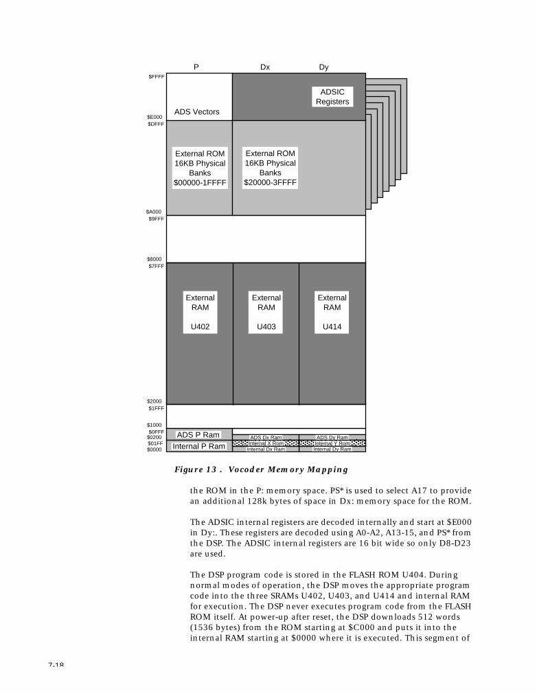
7-18
the ROM in the P: memory space. PS* is used to select A17 to provide an additional 128k bytes of space in Dx: memory space for the ROM.
The ADSIC internal registers are decoded internally and start at $E000 in Dy:. These registers are decoded using A0-A2, A13-15, and PS* from the DSP. The ADSIC internal registers are 16 bit wide so only D8-D23 are used.
The DSP program code is stored in the FLASH ROM U404. During normal modes of operation, the DSP moves the appropriate program code into the three SRAMs U402, U403, and U414 and internal RAM for execution. The DSP never executes program code from the FLASH ROM itself. At power-up after reset, the DSP downloads 512 words (1536 bytes) from the ROM starting at $C000 and puts it into the internal RAM starting at $0000 where it is executed. This segment of
Figure 13 . Vocoder Memory Mapping
$0000$01FF
$0FFF$0200
$1000
$1FFF
$E000$DFFF
$2000
$7FFF
$FFFF
$8000
DyDxP
ADS Vectors
ADSICRegisters
$9FFF$A000
External ROM16KB Physical
Banks$00000-1FFFF
Internal P RamADS P Ram
External ROM16KB Physical
Banks$20000-3FFFF
Internal X Rom Internal Y RomInternal Dx Ram
ADS Dx Ram
Internal Dy Ram
ADS Dy Ram
ExternalRAM
U403
ExternalRAM
U402
ExternalRAM
U414

7-19
program code contains the interrupt vectors and the reset vector and is basically an expanded bootstrap code. When the MCU messages the DSP that the ADSIC has been configured, the DSP overlays more code from the ROM into external SRAM and begins to execute it. Overlays occur at different times when the DSP moves code from the ROM into external SRAM depending on immediate mode of operation, such as changing from transmit to receive.
MCU System Clock The MCU (U204) system clock is provided by circuitry internal to the MCU and is based on the crystal reference, Y201. The nominal operating frequency is 7.3728MHz. This signal is available as a clock at 4XECLK on U204 and is provided to the SLIC (U206) for internal clock timing. The MCU actually operates at a clock rate of 1/4 the crystal reference frequency or 1.8432MHz. This clock is available at ECLK on U204.
The MCU clock contains a crystal warp circuit comprised of L201, Q205, and C228. This circuit is controlled by an I/O port (PA6) on the MCU. This circuit moves the operating frequency of the oscillator about 250ppM on certain receive channels to prevent interference from the MCU bus noise.
DSP System Clock The DSP (U405) system clock, DCLK, is provided by the ADSIC (U406). It is based off the crystal reference, Y401, with a nominal operating frequency of 33.0000MHz. ADSIC contains an internal clock divider circuit which can divide the system clock from 33MHz to 16.5 or 8.25MHz operation. The DSP controls this divider by writing to the ADSIC parallel registers. This frequency is determined by the processes the DSP is running and is generally configured to the slowest operating speed possible to reduce system power consumption.
The additional circuitry of CR402, L403, C459, C467, C491, and C490 make up a crystal warp circuit. This circuit is controlled by the OSCw signal from ADSIC which is configured by the host through the SPI bus. This circuit moves the operating frequency of the oscillator about 400ppM on certain receive channels to prevent interference from the DSP bus noise.
Radio Power-Up/Power-Down Sequence
Radio power-up begins when the user closes the radio on/off switch on the control top. This enables 7.5Vdc on the B+_SENSE signal. This signal enables the pass element Q207 through Q206 enabling SW_B+ to the VOCON board and transceiver board. B+_SENSE also enables the +5Vdc regulator U409. When +5Vdc has been established, it is sensed by the supervisory IC U407. U407 disables the system reset through the delay circuit R481 and C482.
When the MCU comes out of reset, it fetches the reset vector in ROM at $FFFE, $FFFF and begins to execute the code this vector points to. It configures the SLIC through the parallel bus registers. Among other things it enables the correct memory map for the MCU. It configures all the transceiver devices on the SPI bus. The MCU then pulls the ADSIC out of reset and after a minimal delay the DSP also. It then configures the ADSIC through the SPI bus configuring among other

7-20
things, the DSP memory map. While this is happening, the DSP is fetching code from the ROM U404 into internal RAM and beginning to execute it. It then waits for a message from the MCU that the ADSIC has been configured, before going on.
During this process, the MCU does power diagnostics. These diagnostics include verifying the MCU system RAM and verifying the data stored in the internal EEPROM, external EEPROM, and FLASH ROMs. The MCU queries the DSP for proper status and the results of DSP self tests. The DSP self tests include testing the system RAM, verifying the program code in ROM U404, and returning the ADSIC configuration register checksum. Any failures cause the appropriate error codes to be sent to the display. If everything is OK, the appropriate radio state is configured and the unit waits for user input.
On power-down, the user opens the radio on/off switch removing the B+_SENSE signal from the VOCON board. This does not immediately remove power as the MCU holds this line active through B+_CNTL. The MCU then saves pertinent radio status data to the external EEPROM. Once this is done, B+_CNTL is released shutting off SW_B+ at Q207 and shutting down the 5Vdc regulator U409. When the regulator slumps to about 4.6Vdc, the supervisory IC U407 activates a system reset to the SLIC which in turn resets the MCU.
8-1
Secure Modules 8Introduction The secure modules are designed to digitally encrypt and decrypt voice
and ASTRO data in ASTRO SABER™ radios. This section covers the following secure modules:
• NTN7770 • NTN1152
• NTN7771 • NTN1153
• NTN7772 • NTN1158
• NTN7773 • NTN1147
• NTN7774 • NTN1367
• NTN7329 • NTN1368
• NTN7332 • NTN1369
• NTN7331 • NTN1370
• NTN3330 • NTN1371
• NTN7370 • NTN8967
• NTN1146
NOTE: The secure modules are NOT serviceable. Theinformation contained in this chapter is onlymeant to help determine whether a problem is dueto a secure module or the radio itself.
The secure module uses a custom encryption integrated circuit (IC) and an encryption key variable to perform its encode/decode function. The encryption key variable is loaded into the secure module, via the radio’s universal (side) connector, from a hand-held, key variable loader (KVL). The encryption IC corresponds to the particular encryption algorithm purchased. The encryption algorithms and their corresponding kit numbers are:
KITS:
DVP NTN7770
DES NTN7771
DES-XL NTN7772
DVI-XL NTN7773
DVP-XL NTN7774
DVI-XL & DVP NTN7329
DES-XL & DVP NTN7332
DES-XL & DVP-XL NTN7731
DVP & DVP-XL NTN7330
DVP-XL & DVI-XL NTN7370
All, except DVP NTN8967
TANAPAS:
DVP NTN1146
DES NTN1152
DES-XL NTN1153
DVI-XL NTN1158
DVP-XL NTN1147
DVI-XL & DVP NTN1367
DES-XL & DVP NTN1368
DES-XL & DVP-XL NTN1369
DVP & DVP-XL NTN1370
DVP-XL & DVI-XL NTN1371

8-2
Circuit Description The secure module operates from three power supplies (UNSW_B+, SW_B+, and +5V). The +5V and the SW_B+ are turned on and off by the radio’s on/off switch. The UNSW_B+ provides power to the secure module as long as the radio battery is in place.
Key variables are loaded into the secure module through connector J601, pin 15. Up to 16 keys (depending on the type of encryption module) can be stored in the module at a time. The key can be infinite key retention or 30-seconds key retention, depending on how the code plug is setup.
The radio’ s host processor communicates with the Secure Module on the Serial Peripheral Interface (SPI) bus. The host processor is the master on this bus, while the secure module is a slave on the bus. The SPI bus consists of five signal lines. Refer to Table 1 for signal information. A communications failure between the host processor and the secure module will be indicated as an “EEEERRRRRRRROOOORRRR 00009999////11110000” message on the radio display.
TroubleshootingSecure Operations
Refer to the Basic Service Manual, Motorola publication number 68P81076C05 for disassembly and reassembly information. A key variable loader (KVL) and oscilloscope are needed to troubleshoot the secure module.
NOTE: The secure module itself is not serviceable. If thesecure module is found to be defective, it must bereplaced.
Error 09/10, Error 09/90
The ASTRO Digital XTS 3000 radio automatically performs a self test on every power-up. Should the radio fail the self tests, the display will show “EEEERRRRRRRROOOORRRR 00009999////11110000” or “EEEERRRRRRRROOOORRRR 00009999////99990000” accompanied by a short beep. If the display shows “EEEERRRRRRRROOOORRRR 00009999////11110000” or “EEEERRRRRRRROOOORRRR 00009999////99990000,” the radio failed the secure power-up tests and the host microcontroller was unable to communicate with the secure module via the SPI bus. Turn the radio off and back on. If the radio still does not pass the self tests, then a problem exists with the secure operations of the radio.
Troubleshooting information for “EEEERRRRRRRROOOORRRR 00009999////11110000” is found in Troubleshooting Charts.
Keyload When the keyloading cable is attached to the ASTRO Digital XTS 3000 radio and “KKKKEEEEYYYYLLLLOOOOAAAADDDDIIIINNNNGGGG” is not displayed on the radio’s display, then the radio has not gone into KEYLOAD mode. For troubleshooting “KEYLOAD” failure, refer to Troubleshooting Chart, “Key Load Fail.”
NOTE: ASTRO Digital SABER radios need a keyloaderthat has the ability to keyload an ASTRO DigitalSABER radio. The keyloader must be either a “T -- - - CX” or a “T - - - - DX” keyloader.

9-1
TroubleshootingProcedures 9Introduction The purpose of this section is to aid in troubleshooting a malfunctioning
ASTRO Digital SABER radio. It is intended to be detailed enough to localize the malfunctioning circuit and isolate the defective component.
Handling Precautions
Complementary metal-oxide semiconductor (CMOS) devices, and other high-technology devices, are used in this family of radios. While the attributes of these devices are many, their characteristics make them susceptible to damage by electrostatic discharge (ESD) or high-voltage charges. Damage can be latent, resulting in failures occurring weeks or months later. Therefore, special precautions must be taken to prevent device damage during disassembly, troubleshooting, and repair. Handling precautions are mandatory for this radio, and are especially important in low-humidity conditions. DO NOT attempt to disassemble the radio without observing the following handling precautions.
1. Eliminate static generators (plastics, Styrofoam, etc.) in the work area.
2. Remove nylon or double-knit polyester jackets, roll up long sleeves, and remove or tie back loose hanging neckties.
3. Store and transport all static-sensitive devices in ESD-protective containers.
4. Disconnect all power from the unit before ESD- sensitive components are removed or inserted unless otherwise noted.
5. Use a static-safeguarded workstation, which can be accomplished through the use of an anti-static kit (Motorola part number 01-80386A82). This kit includes a wrist strap, two ground cords, a static-control table mat and a static-control floor mat. For additional information, refer to Service and Repair Note SRN-F1052, “Static Control
Most of the ICs are static sensitive devices. Do not attempt to troubleshoot or disassemble a board without first referring to the following Handling Precautions section.
!C a u t i o n

9-2
Equipment for Servicing ESD Sensitive Products,” available from Literature Distribution.
MotorolaLiterature Distribution2290 Hammond DriveSchaumburg, IL 60173(708) 576-2826
6. Always wear a conductive wrist strap when servicing this equipment. The Motorola part number for a replacement wrist strap that connects to the table mat is 42-80385A59.
Voltage Measurement and Signal Tracing
It is always a good idea to check the battery voltage under load. This can be done by measuring the OPT_B+ pin at the universal connector on the back of the radio, with the radio keyed. The battery voltage should remain at or above 7.0Vdc. The battery should be recharged or replaced as necessary prior to analyzing the radio.
In most situations, the problem circuit may be identified using a dc voltmeter, RF millivoltmeter, and oscilloscope (preferably with 100MHz bandwidth or more). The “Recommended Test Equipment, Service Aids, and Tools” section in the ASTRO Digital SABER Portable Radios Basic Service Manual outlines the recommended tools and service aids which would be useful. Of special note is the REX-4200A Housing Eliminator, which allows the technician to open the radio to probe points while in operation.
In some cases dc voltages at probe points are shown in red on the schematics. In other areas diagrams are included to show time varying signals which should be present under the indicated circumstances. It is recommended that a thorough check be made prior to replacement of any IC or part. If the probe point does not have a signal reasonably close to the indicated one, a check of the surrounding components should be made prior to replacing any parts.
When checking a transistor or module, either in or out of circuit, do not use an ohmmeter having more than 1.5 volts dc appearing across test leads or use an ohms scale of less than x100.
!C a u t i o n

9-3
Power-Up Self-Check Errors
Each time the radio is turned on the MCU and DSP perform some internal diagnostics. These diagnostics consist of checking the programmable devices such as the FLASH ROMs, internal and external EEPROMs, SRAM devices, and ADSIC configuration bus checksum. At the end of the power-up self-check routines, if an error exists, the appropriate error code is displayed on the display. For non-display radios, the error codes may be read using the Radio Service Software (RSS) from the SB9600 bus on the universal connector. The following lists valid checksums, the related failure, and a reference section for investigating the cause of the failure.
Error Description PageCode01/81 Chart 6. 01/81 Host ROM Checksum Failure . . . . 10-501/82 Chart 7. 01/82 or 002, External EEPROM
Checksum Failure. . . . . . . . . . . . . . . . . . . 10-601/84 Chart 8. 01/84 SLIC Initialization Failure . . . . . . . 10-601/88 Chart 9. 01/88 MCU (Host µC)
External SRAM Failure . . . . . . . . . . . . . . . 10-701/92 Chart 10. 01/92, Internal EEPROM
Checksum Failure. . . . . . . . . . . . . . . . . . . 10-702/A0 Chart 11. 02/A0, ADSIC Checksum Faiure . . . . . . . 10-802/81 Chart 12. 02/81, DSP ROM Checksum Failure . . . . 10-802/88 Chart 13. 02/88, DSP External SRAM Failure U414. 10-902/84 Chart 14. 02/84, DSP External SRAM Failure U403. 10-902/82 Chart 15. 02/82, DSP External SRAM Failure U402 10-1002/90 Chart 16. 02/90, General DSP Hardware Failure . . 10-1009/10 Chart 17. 09/10, Secure Hardware Failure . . . . . . . 10-1109/90 Chart 18. 09/90, Secure Hardware Failure . . . . . . . 10-11001 Chart 31. VHF/UHF Frequency
Generation Unit (FGU) . . . . . . . . . . . . . 10-19001 Chart 32. 800MHz Frequency
Generation Unit (FGU) . . . . . . . . . . . . . 10-20002 Chart 7. 01/82 or 002, External EEPROM
Checksum Failure. . . . . . . . . . . . . . . . . . . 10-6
In the case of multiple errors, the codes are logically OR’d and the results displayed. As an example, in the case of an ADSIC checksum failure and a DSP ROM checksum failure, the resultant code would be 02/A1. Following is a series of troubleshooting flowcharts which relate to each of these failure codes.
Power-Up Sequence Upon RESET* going active, the MCU begins to execute code which is pointed to by the vector stored at $FFFE, $FFFF in the FLASH ROM. The execution of this code is as follows:
1. Initialize the MCU (U204). Green LED on.
2. Initialize the SLIC (U206).
3. CONFIG register check. If the CONFIG register is not correct, the MCU will repair it and loop.
4. Start ADSIC/DSP:
- Bring the ADSIC reset line high.
- Wait 2ms.
- Bring the DSP reset line high.

9-4
5. Start EMC:
- Set the EMC wake-up line low (emc irq line).
- Wait 5ms.
- Set the EMC wake-up line high.
- Wait 10ms.
- Set the EMC wake-up line low (emc irq line).
- Wait 5ms.
- Set the EMC wake-up line high.
6. Begin power-up self-tests.
7. Begin RAM tests:
- External RAM ($1800-3FFF).
- Internal RAM ($1060-$1300).
- External RAM ($0000-$0DFF).
- Display 01/88 if failure.
The radio will get stuck here if the internal RAM is defective. The radio uses the internal RAM for stack. The RAM routines use subroutines. Thus, if the internal RAM is defective, the radio will get lost testing the external RAM.
8. Display “Self Test” (these routines use subroutines too). It is almost impossible to display an error message if the internal RAM is defective.
9. Begin MCU (host µC) ROM checksum test.
- Fail 01/81 if this routine fails.
10. Begin DSP power-up tests. The MCU will try this five times before it fails the DSP test.
- Check for HF2.
Fail 02/90 if 100ms.
- Program the ADSIC.
- Wait for the DSP power-up message.
- Fail 02/90 if 300ms.
- Fail 02/90 if wrong message from the DSP.
- Wait for the DSP status information.
- Fail 02/90 if 100ms.
- Fail 02/88 if DSP RAM (U414) fails.
- Fail 02/84 if DSP RAM U403 fails.
- Fail 02/82 if DSP RAM U402 fails.

9-5
- Fail 02/81 if DSP RAM fails.
- Wait for the ADSIC checksum.
- Fail 02/90 if 100ms.
- Fail 02/90 if failure.
- Wait for the first part of the DSP version number.
- Fail 02/90 if 100ms.
- Wait for the second part of the DSP version number.
- Fail 02/90 if 100ms.
11. Display errors if a fatal error exists at this point.
12. Checksum the codeplug.
- Test internal codeplug checksums.
- Fail 01/92 if failure.
- Test external codeplug checksums.
- Error 01/82 if non-fatal error; fail 01/82 if fatal error.
13. Power-up the EMC (if it is enabled in the codeplug).
14. Turn off the green LED.
15. Start up operating system.

9-6
Standard Bias Table
Table 3, below, outlines some standard supply voltages and system clocks which should be present under normal operation. These should be checked as a first step to any troubleshooting procedure.
Table 2 . Standard Operating Bias
Signal Name Nominal Value Tolerance Source
UNSW_B+ 7.5Vdc 6.0-9.0Vdc J401
SW_B+ 7.5Vdc 6.0-9.0Vdc Q207
+5V
+5VA
5.0Vdc
5.0Vdc
±10%
±10%
U409
U410
RESET 5.0Vdc +0.7, - 1.0Vdc U407
POR* 5.0Vdc +0.7, - 1.0Vdc U206
DSP_RST*
ADSIC_RST*
5.0Vdc
5.0Vdc
+0.7, -1.0Vdc
+0.7, -1.0Vdc
U204
U204
DCLK 33.0000MHza
a. This is number may vary due to the operating mode of the radio whenit is measured. The ADSIC contains a divider which may divide theclock by a modulus of 2. Therefore the actual frequency measuredmay be clock/2n. The most common frequency will be 16.5000MHznominal.
±500ppM U406
ODC 2.4MHz ±30ppM ABACUS
ECLK
IRQB*
1.8432MHz
8kHzb
b. This 8kHz clock will be present only after the MCU has successfully pro-grammed the ADSIC after power-up. This is a good indication that theADSIC is at least marginally operational.
±500ppM
±500ppM
U204
U406
+5V 5.0Vdc ±10% U202
RX_5Vc
c. Receive mode only.
5.0Vdc ±10% U106

11-1
Troubleshooting Waveforms 11Introduction This section contains images of waveforms which may be useful in
verifying operation of certain parts of the circuitry. These waveforms are for reference only; the actual data depicted will vary depending upon operating conditions.
Waveforms
Figure 14 . Waveform W1
103 AcquisitionsTek stopped:T
1
Ch1
T
M 200us Ch1 -680mV
W1: Switched Regulator Clock OutTrace 1 - (U409)LX measured with radio instandby mode with UNSW_B+ at 7.5VDC.
2.00V
MAEPF-24376-O

11-2
Figure 15 . Waveform W2
2893 AcquisitionsTek stopped:T
2
Ch3Ch1
T
1
3
M 20.0us Ch1 2.2 V
W2: DSP SSI Port RX mode.Receiving1KHz tone @ 3KHz deviation, -60dBm.Trace 1 - RFSTrace 2 - RXDTrace 3 - SCKR (2.4/0.600MHz)
Ch1 Freq19.991kHzLow signalamplitude
5.00V5.00V
1
5.00VCh2
MAEPF-24377-A
Note 1: Typically SCKR is a 2.4 MHz clock. In low powermodes, as shown here, SCKR is 600KHz.
Figure 16 . Waveform W3
T
T
2836 AcquisitionsTek stopped:T
3
Ch1 Ch2Ch3
2
1
M 5.00us Ch1 2.2 V
W3: DSP SSI Port TX mode CSQ.Trace 1 - SC2Trace 2 - STDTrace 3 - SCK (1.2MHz)
Ch1 Freq47.856kHzLow signalamplitude
5.00V 5.00V5.00V
MAEPF-24378-A

11-3
Figure 17 . Waveform W4
T
13 AcquisitionsTek stopped:T
1
Ch1 M 10.0us Ch1 2.2 V
W4: ABACUS programmingcaptured during mode change.Trace 1 - (ADSIC) SBI
MAEPF-24379-O
Ch1 Freq74.610kHz
2.00V
Figure 18 . Waveform W5
34513 AcquisitionsTek stopped:T
3
Ch3
1
2
Ch1 Ch2 M 5.00us Ch1 2.2 V
Note 2: Since these signals are a differentialcurrent loop these voltages are very low.
MAEPF-24380-A
2
W5: ABACUS/ADSIC Interface.Receiving 1KHz tone @ 3KHz deviation,-60dbm.Trace 1 -IDC (2.4MHz)Trace 2 - DOUTTRACE 3 - DOUT*
Ch1 Freq2.251920 MHzLow resolution
2.00V500mV
500mV
T

11-4
Figure 19 . Waveform W6
Tek stopped:T
1
Ch1
T
18 AcquisitionsTek stopped:T
2
Ch2
T
11
13
M 50ns Ch1 2.2 V
W6: SPI Bus Programming ADSIC.Trace 1 - ADSIC_SEL*Trace 2 - SPI_SCKTrace 3 - MOSINote: These waveforms are typical toany device on the SPI bus.
Ch1 Freq= Hz
No periodfound
Ch1Ch3
5.00V5.00V
5.00V
MAEPF-24381-A
T
T
T
Figure 20 . Waveform W7
103 AcquisitionsTek stopped:T
2
Ch2
1
3
4
M 200us Ch1 2.20 V
W7: Receive audio: Receiving1KHz tone @ 3KHz deviation, -60dBm.Trace 1 - IRQB @ DSP (8KHz)Trace 2 - SD0 @ C404Trace 3 - SPKR_COMMONTrace 4 - INT_SPKR
Ch1 Freq7.9118kHzLow signalamplitude
5.00V2.00V
200mV 2.00V
Ch1Ch3
Note 3: Actual level is dependent upon volume setting.
MAEPF-24382-ACh4
3
T
T
T
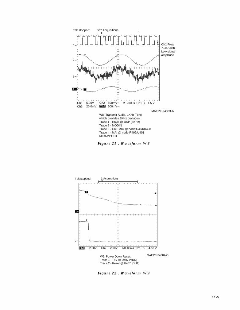
11-5
Figure 21 . Waveform W8
507 AcquisitionsTek stopped:T
1
Ch4
T
2
3
4
M 200us Ch1 1.5 V
W8: Transmit Audio. 1KHz Tonewhich provides 3KHz deviation.Trace 1 - IRQB @ DSP (8KHz)Trace 2 - MODINTrace 3 - EXT MIC @ node C484/R408Trace 4 - MAI @ node R492/U401MICAMPOUT
Ch1 Freq7.9872kHzLow signalamplitude
5.00V20.0mV
MAEPF-24383-A
500mV500mV
Ch1Ch3
Ch2
T
T
Figure 22 . Waveform W9
1 AcquisitionsTek stopped:T
1
Ch1
T
2
M1.00ms Ch1 4.52 V
W9: Power Down Reset.Trace 1 - +5V @ U407 (VDD)Trace 2 - Reset @ U407 (OUT)
2.00V Ch2
MAEPF-24384-O
2.00V
T

11-6
Figure 23 . Waveform W10
493 AcquisitionsTek stopped:
MAEPF-24385-O
T
1
Ch1
T
M 200ns Ch1 1.64 V
W10 ADSIC 2.4 MHz ReferenceTrace 1 - IDC @ U406
Ch1 Freq2.4038MHz
2.00V

12-1
Troubleshooting Diagrams 12Introduction to This Section
This section contains troubleshooting diagrams necessary to isolate a problem to the component level. Use these diagrams in conjunction with the theory of operation, troubleshooting procedures, charts, and waveforms.
Table 3 . J201VOCON Board to Universal Connector
J201 Pin #
Description To/FromUC
Pin #
1 Removed2 n/c3 n/c4 LH DATA/BOOT DATA OUT U208-1 35 EXT MIC U411-6 46 SB9600 BUSY U204-J3 67 OPT SEL 1 U206-G3
(EXT PTT)Q210
7
8 RS232 DATA IN U206-B2 129 OPT SEL2 (KEYLOAD*) U206-C6 1010 KEYFAIL*/RTSIN* U206-J8
J801-159
11 SPKR COMMON U401-A3U204-B3 J701-14
1
12 EXT SPKR U401-A5U204-C4
2
13 OPTB+/BOOT SEL/VPP* CR201/Q21 814 CTSOUT* U206-B6 515 RS232 DATA OUT/BOOT DATA IN U206-A5 11

12-2
Table 4 . J601VOCON Board to Display Board
J601 Pin # Description To/From
1 MOSI U204-J6J801-8J401-9
2 SPI SCK U204-G5 J801-9J401-10
3 SW B+ J401-17
4 DISP EN*/LATCH SEL*
U206-G8
5 DISP RST* U204-F5
6 BL EN U206-E7
7 +5V U409-12
8 n/c
9 +5V U709-9
Table 5 . J701VOCON Board to Keypad
J701 Pin # Description To/From
1 ROW 5/5V-EN* U206-F8
2 GROUND/MIC RETURN
3 ROW 2/SPK EN U206-G4
4 INT MIC U411-2
5 COL2 U206-D5
6 COL3/MOB IRQ* U206-B4
7 GROUND
8 n/c
9 ROW4/TXPA EN* U206-G9
10 COL1 U206-A7
11 ROW3/BUSY OUT U206-K8
12 ROW6/MIC EN U206-G7
13 ROW1 U206-J3
14 SPKR COMMON U401-A3J201-11U401-A3U204-B3
15 INT SPKR U401-B2
Table 6 . J1/J401Transceiver Board to VOCON Board
J1/J401 Pin #
Description TransceievrBoard
VOCONBoard
1 DOUT* U401-4 U406-H3
2 DOUT U401-5 U406-K3
3 GROUND
4 SBI U401-6 U406-J3
5 GROUND
6 POR*RSSI U305-5U503-19
U407-1
7 DA SEL* DA CE
U503-16 U204-H5
8 ODC 2.4MHz U401-7 U406-F3
9 MOSI DATA U503-18U302-2 U304-25
10 SPI SCK* U503-17U302-3U304-22 (CLOCK)
U204-G5
11 ROSC/PSC CE* U304-24 (REF OSC EN)
U204-F6
12 GROUND
13 LOCK DET* U302-41CR502
U206-K2
14 SYN SEL* U302-4 (SYN CE)
U204-H7
15 MOD IN U302-5 U406-B2
16 GROUND
17 SW B+ U305-8 U409, J801-1, Q206
18 GROUND
19 UNSW B+ J3-1 U105-5U502-6 (RAW B+)
U409-1
20 UNSW B+ J3-1 U105-5U502-6 (RAW B+)J801-20
U409-1Q207

12-3
Table 7 . J801VOCON Board to Encryption Board
J801 Pin # Description To/From
1 SW B+ J401-17
2 SW B+ J401-17
3 EMC RXO U405-B7
4 EMC TXO U405-A7
5 n/c
6 GROUND
7 MISO U204-H6
8 MOSI U204-J6J601-1
9 SPI SCK U204-G5 J601-2
10 EMC EN* U206-D6
11 EMC REQ* U206-H3
12 EMC MAKEUP* U206-K7
13 n/c
14 n/c
15 KEYFAIL*/RTSIN* U206-J8
16 n/c
17 n/c
18 n/c
19 n/c
20 UNSW B+ J401-19
21 GROUND
22 GROUND
23 n/c
24 n/c
25 n/c
Table 8 . J901VOCON Board to Control Top Flex
J901 Pin # Description To/From
1 UNSW B+ J401-19
2 TG1/PROG SWITCH U204-D3
3 VOL U204-C3
4 EMERG U204-A3
5 +5V U409-12
6 INT PTT* U204-H2
7 RTA3 U206-H1
8 GRN LED DRIVER U206-E8
9 TG2 A/B SWITCH* U204-A2
10 B+ SENSE
11 RTA0 U206-F3
12 RED LED DRIVER U206-H9
13 RTA1 U206-F4
14 GROUND
15 RTA2* U206-F2
16 n/c
17 n/c
18 n/c
19 n/c
20 UNSW B+ J401-19
21 GROUND
22 GROUND
23 n/c
24 n/c
25 n/c

12-4
Notes

*6881076C10*68P81076C10-A
Motorola8000 West Sunrise BoulevardFort Lauderdale, Florida 33322