digital logic circuitsdigital logic circuits fundamentals ivlsi.hongik.ac.kr/lecture/이전 강의...
TRANSCRIPT
Digital Logic CircuitsDigital Logic CircuitsDigital Logic CircuitsDigital Logic CircuitsFundamentals IFundamentals I
Fundamentals I 1
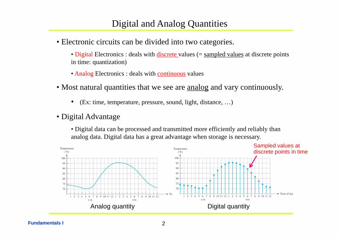
Digital and Analog Quantities
• Electronic circuits can be divided into two categories.• Digital Electronics : deals with discrete values (= sampled values at discrete points in time: quantization)q )
• Analog Electronics : deals with continuous values
• Most natural quantities that we see are analog and vary continuously.
• (Ex: time, temperature, pressure, sound, light, distance, …)
• Digital Advantageg g• Digital data can be processed and transmitted more efficiently and reliably than analog data. Digital data has a great advantage when storage is necessary.
Sampled values atSampled values at discrete points in time
Fundamentals I 2
Analog quantity Digital quantity
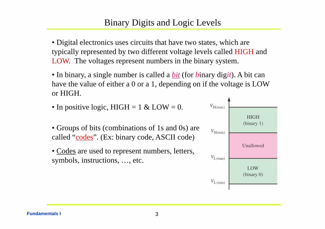
Binary Digits and Logic Levels
• Digital electronics uses circuits that have two states, which are typically represented by two different voltage levels called HIGH and LOW The voltages represent numbers in the binary systemLOW. The voltages represent numbers in the binary system.
• In binary, a single number is called a bit (for binary digit). A bit can have the value of either a 0 or a 1, depending on if the voltage is LOW or HIGH.
• In positive logic, HIGH = 1 & LOW = 0.
• Groups of bits (combinations of 1s and 0s) are called “codes”. (Ex: binary code, ASCII code)( y , )
• Codes are used to represent numbers, letters, symbols, instructions, …, etc.
Fundamentals I 3
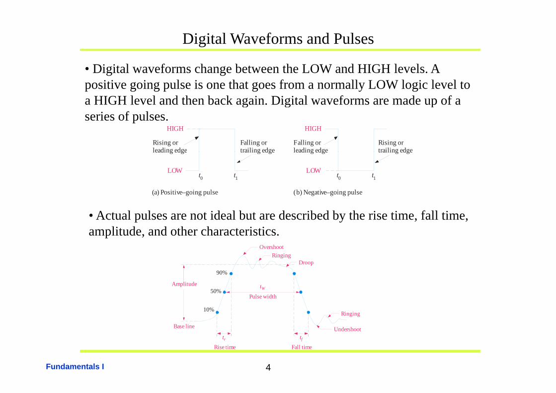
Digital Waveforms and Pulses
• Digital waveforms change between the LOW and HIGH levels. A positive going pulse is one that goes from a normally LOW logic level to a HIGH level and then back again. Digital waveforms are made up of a g g pseries of pulses.
Falling orleading edge
HIGH
Rising ortrailing edge
HIGH
Rising orleading edge
Falling ortrailing edge leading edge
(b) Negative–going pulse
trailing edge
LOW
(a) Positive–going pulse
leading edge trailing edge
LOW t0 t1 t0 t1
• Actual pulses are not ideal but are described by the rise time, fall time, amplitude, and other characteristics.
90%
Amplitude t
OvershootRinging
Droop
50%
10%
Base line
Pulse width
Amplitude tW
Undershoot
Ringing
Fundamentals I 4
Rise time Fall time
tr tfUndershoot
Periodic Pulse Waveforms
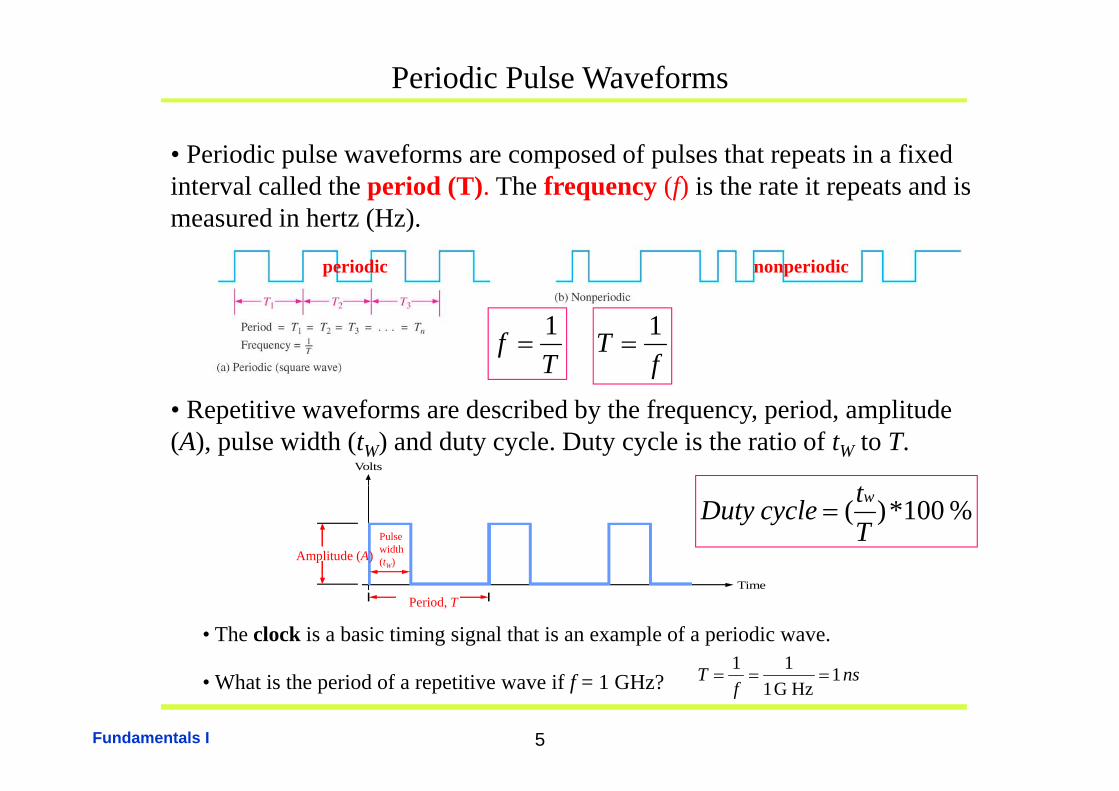
• Periodic pulse waveforms are composed of pulses that repeats in a fixed interval called the period (T). The frequency (f) is the rate it repeats and is measured in hertz (Hz)measured in hertz (Hz).
periodic nonperiodic
Tf 1
fT 1
• Repetitive waveforms are described by the frequency, period, amplitude (A), pulse width (tW) and duty cycle. Duty cycle is the ratio of tW to T.
Volts
% 100*)( TtcycleDuty w
Amplitude (A)
Pulse width (tW)
• The clock is a basic timing signal that is an example of a periodic wave.11
TimePeriod, T
Fundamentals I 5
• What is the period of a repetitive wave if f = 1 GHz? nsf
T 1HzG 1
11
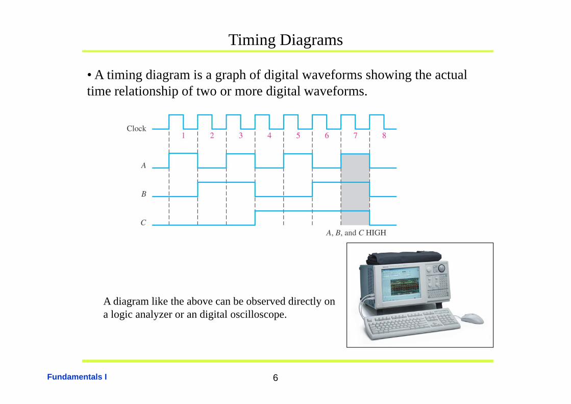
Timing Diagrams
• A timing diagram is a graph of digital waveforms showing the actual time relationship of two or more digital waveforms.
A diagram like the above can be observed directly on a logic analyzer or an digital oscilloscope.
Fundamentals I 6
Data Transfer
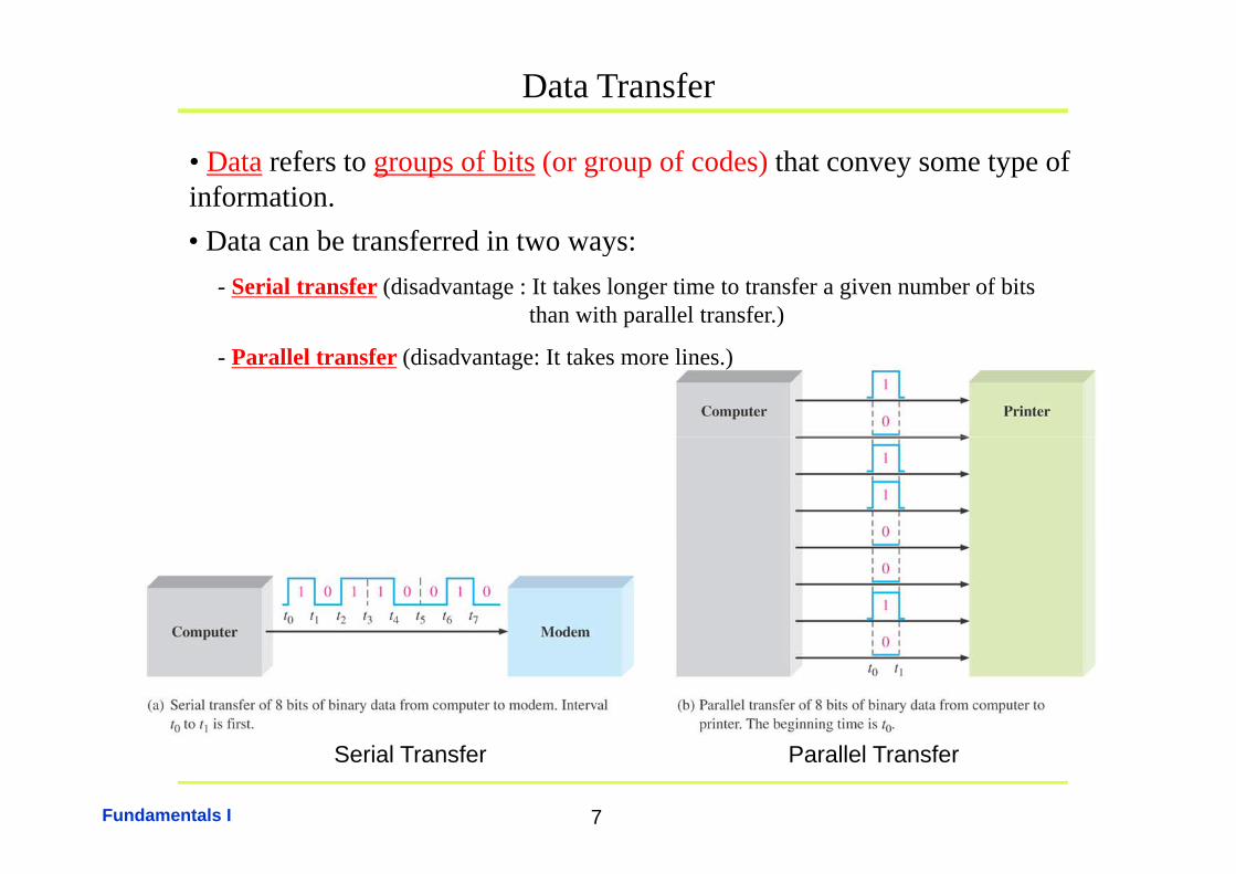
• Data refers to groups of bits (or group of codes) that convey some type of information.• Data can be transferred in two ways:• Data can be transferred in two ways:
- Serial transfer (disadvantage : It takes longer time to transfer a given number of bits than with parallel transfer.)
- Parallel transfer (disadvantage: It takes more lines.)
Fundamentals I 7
Serial Transfer Parallel Transfer
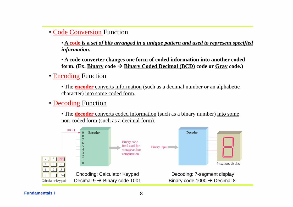
• Code Conversion FunctionCode Conversion Function• A code is a set of bits arranged in a unique pattern and used to represent specified information.
• Encoding Function
• A code converter changes one form of coded information into another coded form. (Ex. Binary code Binary Coded Decimal (BCD) code or Gray code.)
• The encoder converts information (such as a decimal number or an alphabetic character) into some coded form.
• Decoding Function• Decoding Function• The decoder converts coded information (such as a binary number) into some non-coded form (such as a decimal form).
Encoder987654
HIGH
Binary codefor 9 used forstorage and/or
Decoder
Binary input
8 94 5 61 2 30 /
7
43210
storage and/orcomputation
Encoding: Calculator Keypad
7-segment display
Decoding: 7 segment display
Fundamentals I 8
0 . +/–Calculator keypad
Encoding: Calculator KeypadDecimal 9 Binary code 1001
Decoding: 7-segment displayBinary code 1000 Decimal 8
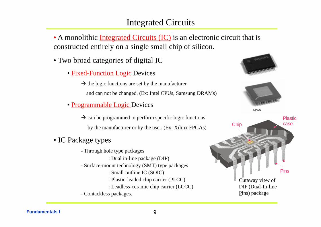
Integrated CircuitsA lithi I t t d Ci it (IC) i l t i i it th t i• A monolithic Integrated Circuits (IC) is an electronic circuit that is
constructed entirely on a single small chip of silicon.
• Two broad categories of digital ICTwo broad categories of digital IC
• Fixed-Function Logic Devices the logic functions are set by the manufacturer
and can not be changed. (Ex: Intel CPUs, Samsung DRAMs)
• Programmable Logic Devices
PlasticcaseChip
can be programmed to perform specific logic functions
by the manufacturer or by the user. (Ex: Xilinx FPGAs)
• IC Package types• IC Package types- Through hole type packages
: Dual in-line package (DIP)Surface mount technology (SMT) type packages
Pins
Cutaway view of DIP (Dual-In-line
- Surface-mount technology (SMT) type packages: Small-outline IC (SOIC): Plastic-leaded chip carrier (PLCC): Leadless-ceramic chip carrier (LCCC)
Fundamentals I 9
Pins) package- Contackless packages.
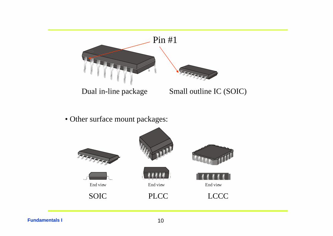
Pi #1Pin #1
Dual in line package Small outline IC (SOIC)Dual in-line package Small outline IC (SOIC)
• Other s rface mo nt packages:• Other surface mount packages:
End viewEnd viewEnd view
SOIC PLCC LCCC
Fundamentals I 10
SOIC PLCC LCCC
Introduction to Programmable Logic
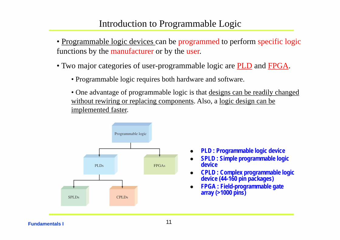
• Programmable logic devices can be programmed to perform specific logic functions by the manufacturer or by the user.
• Two major categories of user programmable logic are PLD and FPGA• Two major categories of user-programmable logic are PLD and FPGA.
• Programmable logic requires both hardware and software.
• One advantage of programmable logic is that designs can be readily changed• One advantage of programmable logic is that designs can be readily changed without rewiring or replacing components. Also, a logic design can be implemented faster.
PLD : Programmable logic device SPLD : Simple programmable logic
device CPLD : Complex programmable logic CPLD : Complex programmable logic
device (44-160 pin packages) FPGA : Field-programmable gate
array (>1000 pins)
Fundamentals I 11
FPGA
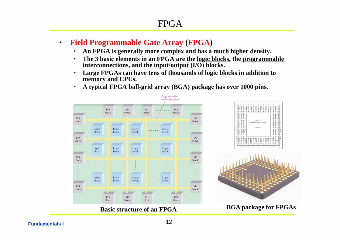
• Field Programmable Gate Array (FPGA)• An FPGA is generally more complex and has a much higher density.• The 3 basic elements in an FPGA are the logic blocks, the programmable
interconnections and the input/output (I/O) blocksinterconnections, and the input/output (I/O) blocks.• Large FPGAs can have tens of thousands of logic blocks in addition to
memory and CPUs.• A typical FPGA ball-grid array (BGA) package has over 1000 pins.
Fundamentals I 12
Basic structure of an FPGA BGA package for FPGAs
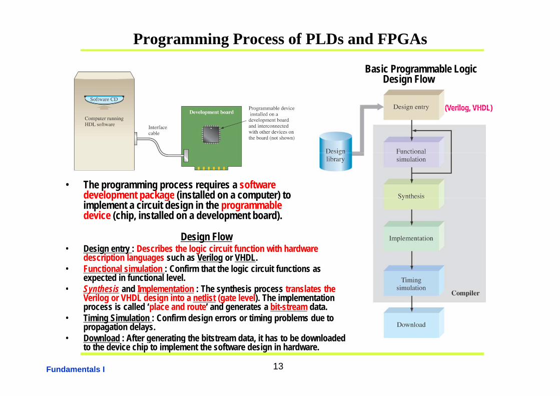
Programming Process of PLDs and FPGAs
(Verilog VHDL)
Basic Programmable Logic Design Flow
(Verilog, VHDL)
• The programming process requires a software development package (installed on a computer) to development package (installed on a computer) to implement a circuit design in the programmable device (chip, installed on a development board).
Design Flow• Design entry : Describes the logic circuit function with hardware
description languages such as Verilog or VHDL.• Functional simulation : Confirm that the logic circuit functions as
expected in functional level.• Synthesis and Implementation : The synthesis process translates the • Synthesis and Implementation : The synthesis process translates the
Verilog or VHDL design into a netlist (gate level). The implementation process is called ‘place and route’ and generates a bit-stream data.
• Timing Simulation : Confirm design errors or timing problems due to propagation delays.
Fundamentals I 13
• Download : After generating the bitstream data, it has to be downloaded to the device chip to implement the software design in hardware.
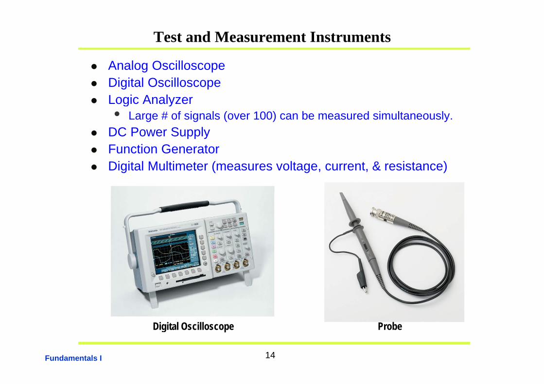
Test and Measurement Instruments
A l O ill Analog Oscilloscope Digital Oscilloscope Logic Analyzerg y
• Large # of signals (over 100) can be measured simultaneously. DC Power Supply Function Generator Function Generator Digital Multimeter (measures voltage, current, & resistance)
Di it l O ill P b
Fundamentals I 14
Digital Oscilloscope Probe
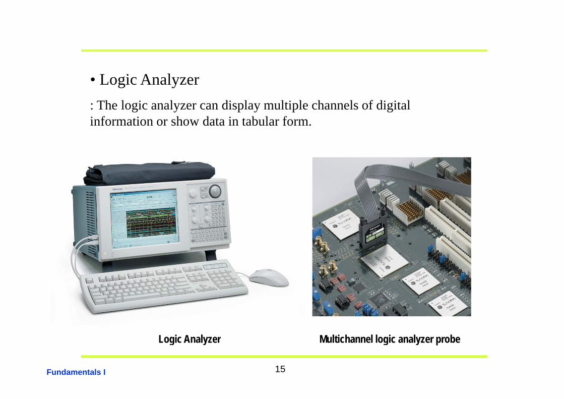
• Logic Analyzer: The logic analyzer can display multiple channels of digital: The logic analyzer can display multiple channels of digital information or show data in tabular form.
L i A l M lti h l l i l b
Fundamentals I 15
Logic Analyzer Multichannel logic analyzer probe
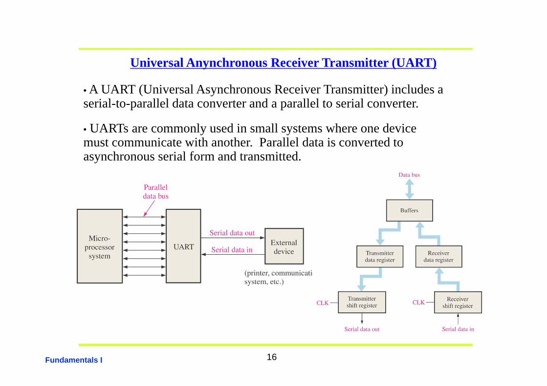
Universal Anynchronous Receiver Transmitter (UART)Universal Anynchronous Receiver Transmitter (UART)
• A UART (Universal Asynchronous Receiver Transmitter) includes a serial-to-parallel data converter and a parallel to serial converterserial to parallel data converter and a parallel to serial converter.
• UARTs are commonly used in small systems where one device must communicate with another. Parallel data is converted to asynchronous serial form and transmitted.
Fundamentals I 16