digital design (vimiaa01) introduction to the verilog...
TRANSCRIPT

BME-MITFPGA labor
Digital Design (VIMIAA01)Introduction to the Verilog HDL
BUDAPEST UNIVERSITY OF TECHNOLOGY AND ECONOMICSFACULTY OF ELECTRICAL ENGINEERING AND INFORMATICS
DEPARTMENT OF MEASUREMENT AND INFORMATION SYSTEMS
Tamás RaikovichBUTE DMIS

BME-MITFPGA labor
Hardware Description Languages
• Hardware description languages have been developed for modeling and simulating hardware functions
• Only a part of the language elements can be used for design implementation
• Difference between standard programming languages and hardware description languages:– Standard programming languages: sequential– HDLs: describe parallel and concurrent behavior
• Two important HDLs:– Verilog– VHDL
1
BME-MITFPGA labor
Verilog HDL
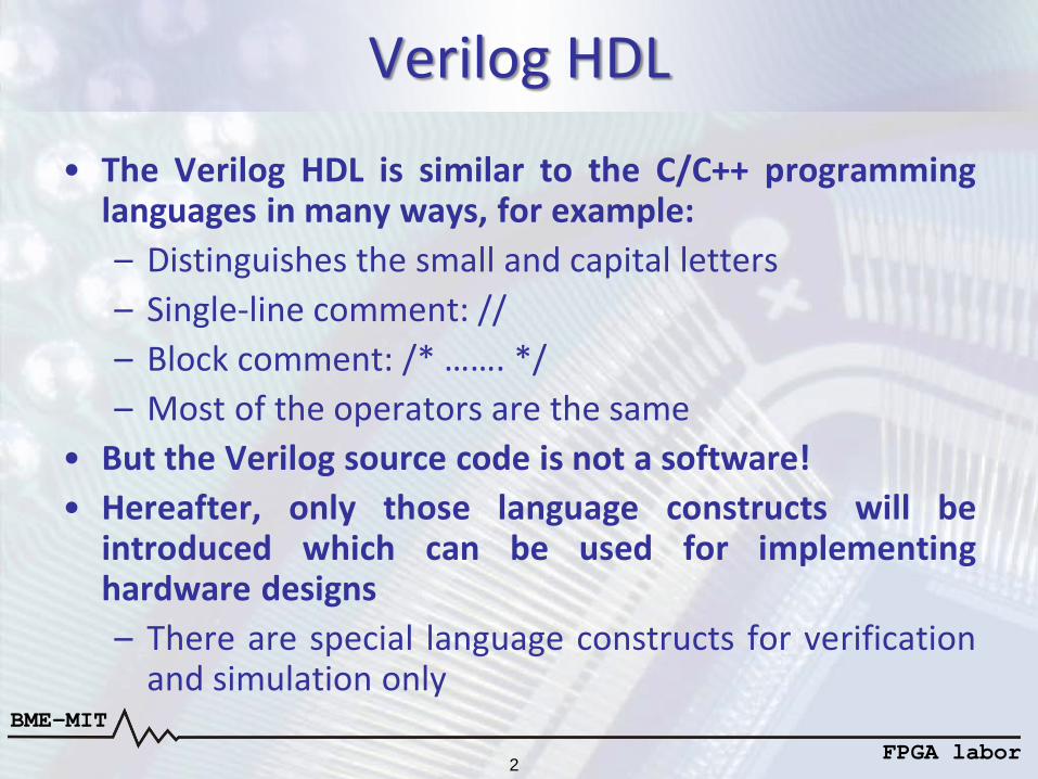
• The Verilog HDL is similar to the C/C++ programminglanguages in many ways, for example:– Distinguishes the small and capital letters– Single-line comment: //– Block comment: /* ……. */– Most of the operators are the same
• But the Verilog source code is not a software!• Hereafter, only those language constructs will be
introduced which can be used for implementinghardware designs– There are special language constructs for verification
and simulation only
2

BME-MITFPGA labor
Verilog HDL - Modules• Verilog language uses a hierarchical, functional unit based
design approach:– The whole design consists of several smaller modules– The complexity of the modules is decided by the designer
• Verilog module:– Definition of the input and output ports, through which
the module is connected to the ”outside world”– Definition of the logical relationship between the input
and output ports
ADD
SUB
MUL
DIV
MUX
OPERATIONOPERAND1
OPERAND2RESULT
ALU
3
BME-MITFPGA labor
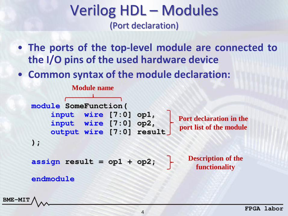
Verilog HDL – Modules(Port declaration)
• The ports of the top-level module are connected tothe I/O pins of the used hardware device
• Common syntax of the module declaration:
module SomeFunction(input wire [7:0] op1,input wire [7:0] op2,output wire [7:0] result
);
assign result = op1 + op2;
endmodule
Module name
Port declaration in theport list of the module
Description of thefunctionality
4

BME-MITFPGA labor
Verilog HDL – Modules(Port declaration)
• Port declaration syntax:<direction> <data_type> <size> <port_name>;
• Direction:– Input port: input– Output port: output– Bi-directional: inout
• Data type: wire is the default data type when omitted– wire: behaves as its name says– reg: not always becomes a real register (data storage element)
• Only output ports and internal signals can be reg type• Signed type:
– The signed keyword indicates that the signal represents a two’scomplement signed value
• Size: [j : i] → The size of the port is |j – i| + 1 bits– The rightmost bit is the j-th bit (j ≤ i is also allowed)– The leftmost bit is the i-th bit– Swapping the indices doesn’t affect the bit order
5

BME-MITFPGA labor
Verilog HDL – Modules(Port declaration)
• Examples:– 1-bit input port: input wire sel;– 16-bit output register: output reg [15:0] result;
• Older syntax of the port declaration:
module SomeFunction(op1, op2, result);
input wire [7:0] op1;input wire [7:0] op2;output wire [7:0] result;
assign result = op1 + op2;
endmodule
Module name Port list
Port declaration
Description of thefunctionality
Optional
6

BME-MITFPGA labor
Verilog HDL – Modules(Module instantiation)
• Module to be instantiated:module SomeFunction(input A, input B, output C);
endmodule
• This can be instantiated (i.e. can be used) in othermodules by the following way:wire d, e, f;SomeFunction Func1(.A(f), .B(e), .C(d));
• More instances can be created from a module, butevery instance name must be different
Module to instantiate Instancename
The signal f is connected to the port A
Associating signals with ports
7

BME-MITFPGA labor
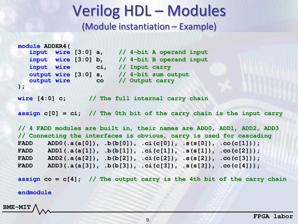
Verilog HDL – Modules(Module instantiation – Example)
• Problem: create a 4-bit binary adder by cascading 4single-bit full adders (FADD)
• The header of the single-bit full adder (FADD)modulemodule FADD(
input wire a, // ”a” operandinput wire b, // ”b” operandinput wire ci, // Input carryoutput wire s, // Sum outputoutput wire co // Output carry
);
• 4 FADD adders have to be instantiated in themodule which implements the 4-bit adder
8
BME-MITFPGA labor
Verilog HDL – Modules(Module instantiation – Example)
module ADDER4(input wire [3:0] a, // 4-bit A operand inputinput wire [3:0] b, // 4-bit B operand inputinput wire ci, // Input carryoutput wire [3:0] s, // 4-bit sum outputoutput wire co // Output carry
);
wire [4:0] c; // The full internal carry chain
assign c[0] = ci; // The 0th bit of the carry chain is the input carry
// 4 FADD modules are built in, their names are ADD0, ADD1, ADD2, ADD3// Connecting the interfaces is obvious, carry is used for cascadingFADD ADD0(.a(a[0]), .b(b[0]), .ci(c[0]), .s(s[0]), .co(c[1]));FADD ADD1(.a(a[1]), .b(b[1]), .ci(c[1]), .s(s[1]), .co(c[2]));FADD ADD2(.a(a[2]), .b(b[2]), .ci(c[2]), .s(s[2]), .co(c[3]));FADD ADD3(.a(a[3]), .b(b[3]), .ci(c[3]), .s(s[3]), .co(c[4]));
assign co = c[4]; // The output carry is the 4th bit of the carry chain
endmodule
9

BME-MITFPGA labor
Verilog HDL – Modules(Internal signal declaration)
• Internal signal declaration syntax:<data_type> <size> <signal_name>;
• Same as the port declaration, but there is nodirection specification and the data type cannotbe omitted
• Examples:– 1-bit wire: wire counter_enable;– 16-bit register: reg [15:0] counter;
10

BME-MITFPGA labor
Verilog HDL – Constants(Possible signal values)
• In the Verilog language, signals can have four values– 0: logic low level– 1: logic high level– z: high-impedance state– x: unknown, cannot be determined, don’t care
• In case of the modern hardware system design, the zvalue (high-impedance state) is used only forimplementing I/O interfaces
• In case of hardware implementation, the x value (don’tcare) can be used only to simplify the description (casexinstruction)
11

BME-MITFPGA labor
Verilog HDL – Constants(Numeric constants)
• Numeric constant definition syntax:<–><bit_number> ’<s><number_system><numeric_constant>
• The signed constants are two’s complement codes• Minus sign: generates the two’s complement of the constant• Bit number: size of the constant in bits
– The default size is 32 bits if omitted• Signed constant: indicated by the s character
– The constant is unsigned if omitted– The sign bit has to be interpreted according to the bit number– The sign extension is automatic in case of the signed constants
• Number system: decimal is the default if omitted– Binary: b, octal: o, decimal: d, hexadecimal: h
• The ’_’ character can be used for separating the digits– This produces a more readable and cleaner code
12

BME-MITFPGA labor
Verilog HDL – Constants(Numeric constants – Examples)
Examples:• 8’b0000_0100: 8-bit binary constant, its decimal value is 4• 6’h1f: 6-bit hexadecimal constant, its decimal value is 31
– In binary: 6’b01_1111• 128: 32-bit decimal constant
– In binary: 32’b00000000_00000000_00000000_10000000• – 4’sd15: 4-bit decimal constant, its value is 1
– The 4’sd15 itself in binary is 4’sb1111, i.e. –1 (signed!)– The minus sign generates the 2’s complement → 4’sb0001
Examples for the sign extension (repeating the original MSb bit):wire [7:0] a = 4’d9; //a=6’b0000_1001 (9)wire [7:0] b = 4’sd5; //b=6’b0000_0101 (5)wire [7:0] c = 4’sd9; //c=6’b1111_1001 (-7)wire [7:0] d = -4’d6; //d=6’b1111_1010 (-6)
13

BME-MITFPGA labor
Verilog HDL – Konstansok(String constants)
• String (text) constant declaration syntax:”characters_of_the_string”
• Very useful for simulating controllers: can be used todisplay the states as text
• The characters of the strings are mapped to their 8-bitASCII codes, therefore the bit number of the stringconstant is 8 times the number of characters
• The upper 8 bits have the value of the first character• Example:
wire [23:0] str = ”HDL”;//str[7:0] = 8’b0100_1100 (’L’)//str[15:8] = 8’b0100_0100 (’D’)//str[23:16] = 8’b0100_1000 (’H’)
14

BME-MITFPGA labor
Verilog HDL – Parameters(Parameter declaration)
• Parameter definition syntax:parameter <name> = <constant>;localparam <name> = <constant>;
• The parameter name can be used as a constant in themodule where the parameter is declared
• Normal parameters: their default value can be changedwhen the module is instantiated
• Local parameters: their value cannot be changed• Example:
parameter WIDTH = 8;
wire [WIDTH-1:0] data;
15
BME-MITFPGA labor
Verilog HDL – Parameters(Parameter declaration)
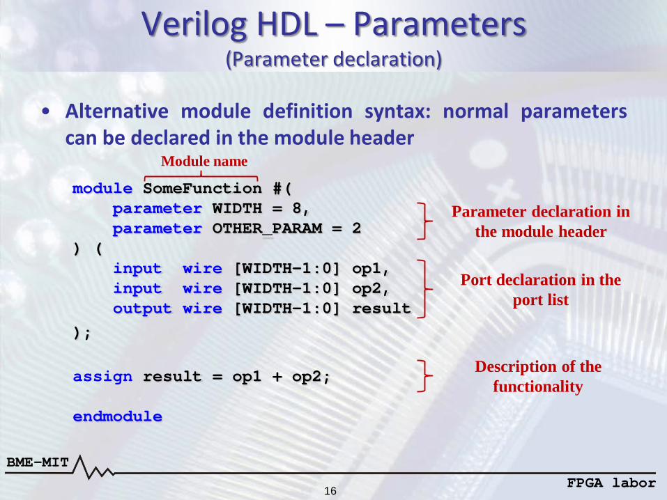
• Alternative module definition syntax: normal parameterscan be declared in the module header
module SomeFunction #(parameter WIDTH = 8,parameter OTHER_PARAM = 2
) (input wire [WIDTH-1:0] op1,input wire [WIDTH-1:0] op2,output wire [WIDTH-1:0] result
);
assign result = op1 + op2;
endmodule
Module name
Port declaration in theport list
Description of thefunctionality
Parameter declaration inthe module header
16
BME-MITFPGA labor
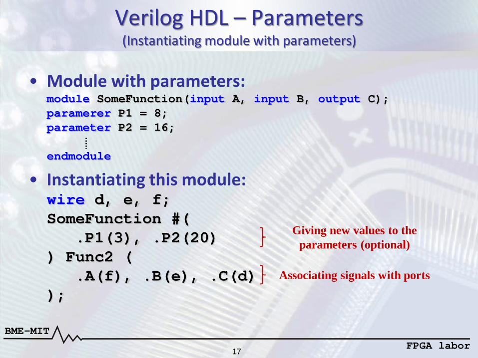
Verilog HDL – Parameters(Instantiating module with parameters)
• Module with parameters:module SomeFunction(input A, input B, output C);paramerer P1 = 8;parameter P2 = 16;
endmodule
• Instantiating this module:wire d, e, f;SomeFunction #(
.P1(3), .P2(20)) Func2 (
.A(f), .B(e), .C(d));
Giving new values to theparameters (optional)
Associating signals with ports
17

BME-MITFPGA labor
Verilog HDL - Operators• The Verilog operators can have 1, 2 or 3 operands• On the right side of the expressions, wire type, reg type and
constant operands can appear• If an operation requires same operand size, the smaller
operand usually zero-extended to the size of the largeroperand
• The expression evaluation is done by the normal precedencerules (the precedence can be controlled using brackets)
Operator Precedence
Unary +, -, !, ~ 1. (highest)
*, /, % 2.
Binary +, - 3.
<<, >>, <<<, >>> 4.
<, <=, >, >= 5.
==, !=, ===, !== 6.
Operator Precedence
&, ~& 7.
^, ~^ 8.
|, ~| 9.
&& 10.
|| 11.
? : (conditional op.) 12. (lowest)
18
BME-MITFPGA labor
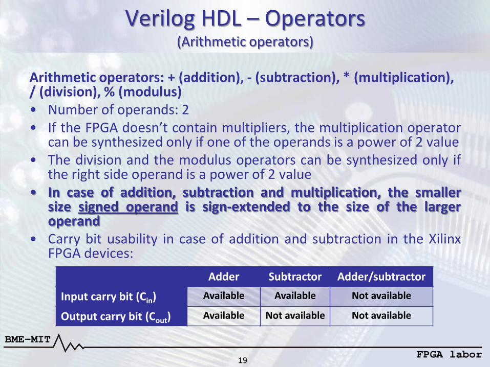
Verilog HDL – Operators(Arithmetic operators)
Arithmetic operators: + (addition), - (subtraction), * (multiplication),/ (division), % (modulus)• Number of operands: 2• If the FPGA doesn’t contain multipliers, the multiplication operator
can be synthesized only if one of the operands is a power of 2 value• The division and the modulus operators can be synthesized only if
the right side operand is a power of 2 value• In case of addition, subtraction and multiplication, the smaller
size signed operand is sign-extended to the size of the largeroperand
• Carry bit usability in case of addition and subtraction in the XilinxFPGA devices:
Adder Subtractor Adder/subtractor
Input carry bit (Cin) Available Available Not available
Output carry bit (Cout) Available Not available Not available
19

BME-MITFPGA labor
Verilog HDL – Operators(Concatenation operator)
• Concatenation operator: { }– Appending multiple operands{5’b10110, 2’b10, 1’b0, 1’b1} = 9’b1_0110_1001
– The same operand can be concatenated multiple times{4{3’b101}} = 12’b101_101_101_101
• Important use cases:– Sign extension: the sign bit must be copied to the upper bitswire [3:0] s_4bit; //4-bit signedwire [7:0] s_8bit; //8-bit signedassign s_8bit = {{4{s_4bit[3]}}, s_4bit};
– Masking a vector with a single bit: without concatenation, the smallersingle-bit operand would be zero-extended to the size of the largeroperandwire [3:0] data;wire [3:0] mdata;wire enable;assign mdata = data & enable; //Wrong!!!assign mdata = data & {4{enable}}; //Correct
20
BME-MITFPGA labor
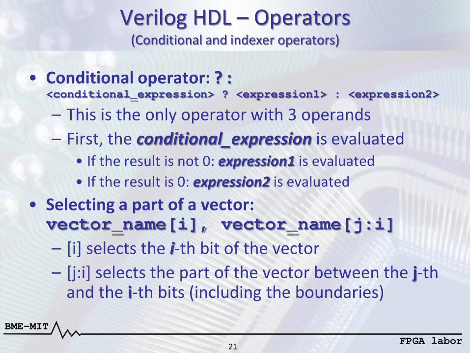
Verilog HDL – Operators(Conditional and indexer operators)
• Conditional operator: ? :<conditional_expression> ? <expression1> : <expression2>
– This is the only operator with 3 operands– First, the conditional_expression is evaluated
• If the result is not 0: expression1 is evaluated• If the result is 0: expression2 is evaluated
• Selecting a part of a vector:vector_name[i], vector_name[j:i]– [i] selects the i-th bit of the vector– [j:i] selects the part of the vector between the j-th
and the i-th bits (including the boundaries)
21
BME-MITFPGA labor
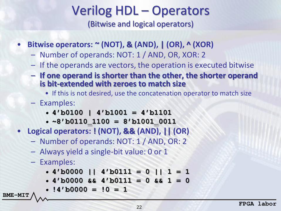
Verilog HDL – Operators(Bitwise and logical operators)
• Bitwise operators: ~ (NOT), & (AND), | (OR), ^ (XOR)– Number of operands: NOT: 1 / AND, OR, XOR: 2– If the operands are vectors, the operation is executed bitwise– If one operand is shorter than the other, the shorter operand
is bit-extended with zeroes to match size• If this is not desired, use the concatenation operator to match size
– Examples:• 4’b0100 | 4’b1001 = 4’b1101• ~8’b0110_1100 = 8’b1001_0011
• Logical operators: ! (NOT), && (AND), || (OR)– Number of operands: NOT: 1 / AND, OR: 2– Always yield a single-bit value: 0 or 1– Examples:
• 4’b0000 || 4’b0111 = 0 || 1 = 1• 4’b0000 && 4’b0111 = 0 && 1 = 0• !4’b0000 = !0 = 1
22

BME-MITFPGA labor
Verilog HDL – Operators(Bit reduction operators)
• Bit reduction operators:& (AND), ~& (NAND), | (OR), ~| (NOR), ^ (XOR), ~^ (NXOR)– Number of operands: 1– Perform a bitwise operation on a single vector– Yield a 1-bit result: 0 or 1– Examples:
• &4’b0101 = 0 & 1 & 0 & 1 = 0• |4’b0101 = 0 | 1 | 0 | 1 = 1
• Important use cases:– Testing for 0 value: NOR connection of the bits
wire [11:0] data;wire all_zeros = ~|data;
– Testing for 2N-1 value (all 1s): AND connection of the bitswire all_ones = &data;
– Indicating the final state (terminal count) of the counter:wire tc = (dir) ? (&cnt) : (~|cnt);
23

BME-MITFPGA labor
Verilog HDL – Operators(Shift operators)
• Logical shift operators: << (left), >> (right)– Number of operands: 2– Examples:
• 8’b0011_1100 >> 2 = 8’b0000_1111• 8’b0011_1100 << 2 = 8’b1111_0000
• Arithmetic shift operators: <<< (left), >>> (right)– Number of operands: 2– The arithmetic left shift is the same as the logical left shift– In case of unsigned operands, the arithmetic right shift is the
same as the logical right shift– In case of signed operand, the arithmetic right shift replicates
the sign bit to fill in the vacant positions (sign extension)– Examples:
• 8’b1001_1100 >>> 2 = 8’b0010_0111• 8’sb1001_1100 >>> 2 = 8’b1110_0111
24

BME-MITFPGA labor
Verilog HDL – Operators(Relational operators)
• Relational operators:== (equality), != (inequality), < (less than), > (greater than),<= (less than or equal), >= (greater than or equal)– Number of operands: 2– The result is always a single-bit value: 0 or 1– The equality and inequality relations are mapped to
gate based logic and usually, the less than and greaterthan relations are mapped to an arithmetic function
– The smaller signed operand is sign extended to thelarger operand to match the size
– Example:• (4’b1011 < 4’b0111) = 0• (4’b1011 != 4’b0111) = 1
25
BME-MITFPGA labor
Verilog HDL - Assignments
• Specifying the logic connection in case of wire signals:assign <wire_signal> = <expression>;– The value of the left wire_signal is determined in every
moment by the right expression (combinational logic)– Example:
wire [15:0] a, b, c;assign c = a & b;
– The logic connection can be specified at the declaration:wire [15:0] a, b;wire [15:0] c = a & b;
• Assigning a value to a reg type signal can be done in thealways blocks using the blocking (=) or non-blocking (<=)assignment operators
26
BME-MITFPGA labor
Verilog HDL – Assignments(Interpretation of the always block by the simulator/verilog parser)
• Always block:always @(sensitivity list)
assignments– The sensitivity list determines the events when the
assignments are evaluated:• always @(a, b, c): the assignments are evaluated
when the value of the a, b or c input signals is changed• always @(*): the assignments are evaluated when one
of the always block input signals is changed• always @(posedge clk): the assignments are
evaluated at the rising edge of the clk signal and the outputis changed only this time
• always @(negedge clk, posedge rst):the assignments are evaluated at the falling edge of clk or when the rst signal is set to 1
27

BME-MITFPGA labor
Verilog HDL – Assignments(Interpretation of the always block by the synthesis tool)
• Always block:always @(sensitivity list)
assignments– The sensitivity list determines what kind of logic element is
used for implementing the behavioral description:• always @(a, b, c): the combinational function of the a, b
and c input signals is specified• always @(*): like the previous one, the vaue of the output is
changed when an input is changed (combinational logic)• always @(posedge clk): we want to use a rising clock edge
sensitive flip-flop or register elements, the inputs are sampled andthe outputs are changed only this time
• always @(negedge clk, posedge rst):like the previousone, the operation is controlled by the falling edge of the clk butthere is also a rst signal which becomes effective if it is set to 1
28

BME-MITFPGA labor
Verilog HDL – Assignments(Using the always block for synthesis)
• Always block:– In case of synthesis, value can be assigned to a reg type
signal only one place in only one always block– The if…else, the case and the for instructions can be used
only in always blocks– Multiple statements inside the always block must be
grouped using begin and end keywords– Example:
wire a;reg b, c, d;
//Prohibited 2nd assignmentalways @(a, b) always @(*)begin begin
c <= a & b; c <= b ^ d;d <= a | b; end
end//C is an AND gate //Here, C is an XOR gate//Peer descriptions. Which one takes effect?
29
BME-MITFPGA labor
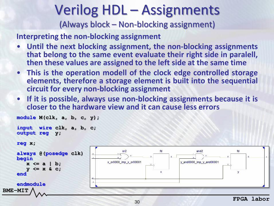
Verilog HDL – Assignments(Always block – Non-blocking assignment)
Interpreting the non-blocking assignment• Until the next blocking assignment, the non-blocking assignments
that belong to the same event evaluate their right side in paralell,then these values are assigned to the left side at the same time
• This is the operation modell of the clock edge controlled storageelements, therefore a storage element is built into the sequentialcircuit for every non-blocking assignment
• If it is possible, always use non-blocking assignments because it iscloser to the hardware view and it can cause less errors
module M(clk, a, b, c, y);
input wire clk, a, b, c;output reg y;
reg x;
always @(posedge clk)begin
x <= a | b;y <= x & c;
end
endmodule
30

BME-MITFPGA labor
Verilog HDL – Assignments(Always block – Blocking assignment)
Interpreting the blocking assignment• The blocking assignment operator (=) is the usual assignment, they are
executed sequentially in order they are written and the new value of theleft side variable is used for evaluating the next expressions
• Therefore, if the result of a blocking assignment is used in the samealways block (in the same clock cycle) later, no storage element is builtinto the sequential circuit for the later assignment (see the signal x in theexample)
module M(clk, a, b, c, y);
input wire clk, a, b, c;output reg y;
reg x;
always @(posedge clk)begin
x = a | b;y = x & c;
end
endmodule
No register for the signal x
31

BME-MITFPGA labor
Verilog HDL – Assignments(Example)
Example: 3-bit shift register• Look at the difference between the two solution• Only using the non-blocking assignments results in the correct circuit
module shr_3bit(clk, si, q0, q1, q2);
input wire clk, si;output reg q0, q1, q2;
always @(posedge clk)begin
q0 <= si; // new q0 ← actual siq1 <= q0; // new q1 ← actual q0q2 <= q1; // new q2 ← actual q1
end // and updates
endmodule
module shr_3bit(clk, si, q0, q1, q2);
input wire clk, si;output reg q0, q1, q2;
always @(posedge clk)begin
q0 = si; // q0 ← siq1 = q0; // q1 ← q0 ← siq2 = q1; // q0 ← q1 ← q0 ← si
end // Three same bit
endmodule
32

BME-MITFPGA labor
Verilog HDL – IF instruction
• Syntax of the if instruction:if (expression) instruction1; [else instruction2;]
– First, the given expression is evaluated:• If its value is not 0: instruction1 is executed• If its value is 0: instruction2 is executed
– The else path is optional, it can be omitted– Multiple statements inside the if instruction must
be grouped using begin and end keywords– The nested if instructions result in hierarchical,
sequential evaluation → PRIORITY!!!!• This is the typical implementation of the control signals
of the functional elements
33
BME-MITFPGA labor
Verilog HDL – CASE instruction• Syntax of the case instruction:
case (expression)alternative1: instruction1;alternative2: instruction2;
[default : default_instruction;]endcase
– The value of the expression is compared with the alternativesin order they are listed (their order may mean priority!)
– The instruction belonging to the first matching alternative isexecuted
– If there is no matching alternative, the default_instruction isexecuted written after the default keyword (optional)
– Multiple instructions must be grouped using begin and endkeywords
– In case of the casex instruction, the alternatives can contain x(don’t care) value also, this may result in simpler description
34
BME-MITFPGA labor
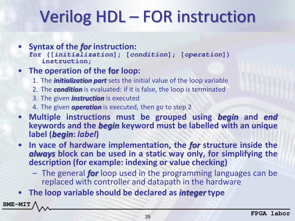
Verilog HDL – FOR instruction• Syntax of the for instruction:
for ([initialization]; [condition]; [operation])instruction;
• The operation of the for loop:1. The initialization part sets the initial value of the loop variable2. The condition is evaluated: if it is false, the loop is terminated3. The given instruction is executed4. The given operation is executed, then go to step 2
• Multiple instructions must be grouped using begin and endkeywords and the begin keyword must be labelled with an uniquelabel (begin: label)
• In vace of hardware implementation, the for structure inside thealways block can be used in a static way only, for simplifying thedescription (for example: indexing or value checking)– The general for loop used in the programming languages can be
replaced with controller and datapath in the hardware• The loop variable should be declared as integer type
35

BME-MITFPGA labor
Verilog HDL – FOR instruction
module RegFile(clk,addr,we,din,r0,r1,r2,r3);
input wire clk, we;input wire [1:0] addr;input wire [7:0] din;output wire [7:0] r0, r1, r2, r3;
reg [7:0] r [3:0]; //4 x 8 bit reg. fileinteger i; //Loop variable
always @(posedge clk)for (i=0; i<4; i=i+1)
if (we && (addr == i))r[i] <= din;
assign {r3,r2,r1,r0} = {r[3],r[2],r[1],r[0]};
endmodule
module BitReverse(din, dout);
input wire [31:0] din;output reg [31:0] dout;
integer i; //Loop variable
always @(*)for (i=0; i<32; i=i+1)begin: reverse_loop
dout[i] <= din[31-i];end
endmodule
• First example: reversing the bit order– The for loop is used for indexing– Without the loop, 32 assignments would be required
• Second example: 4 x 8 bit register file– The for loop is used for indexing and checking equality– Without the loop, 4 conditional assignments would be required
36
BME-MITFPGA labor
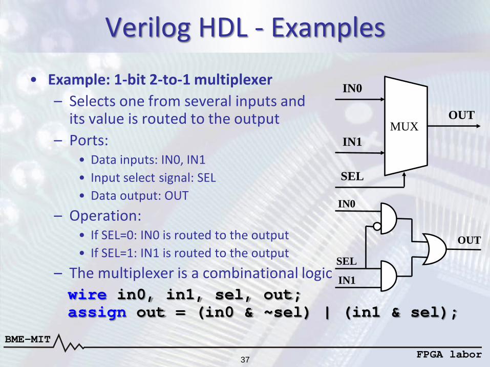
Verilog HDL - Examples
• Example: 1-bit 2-to-1 multiplexer– Selects one from several inputs and
its value is routed to the output– Ports:
• Data inputs: IN0, IN1• Input select signal: SEL• Data output: OUT
– Operation:• If SEL=0: IN0 is routed to the output• If SEL=1: IN1 is routed to the output
– The multiplexer is a combinational logicwire in0, in1, sel, out;assign out = (in0 & ~sel) | (in1 & sel);
MUX
IN0
IN1
SEL
OUT
OUT
IN0
IN1
SEL
37
BME-MITFPGA labor
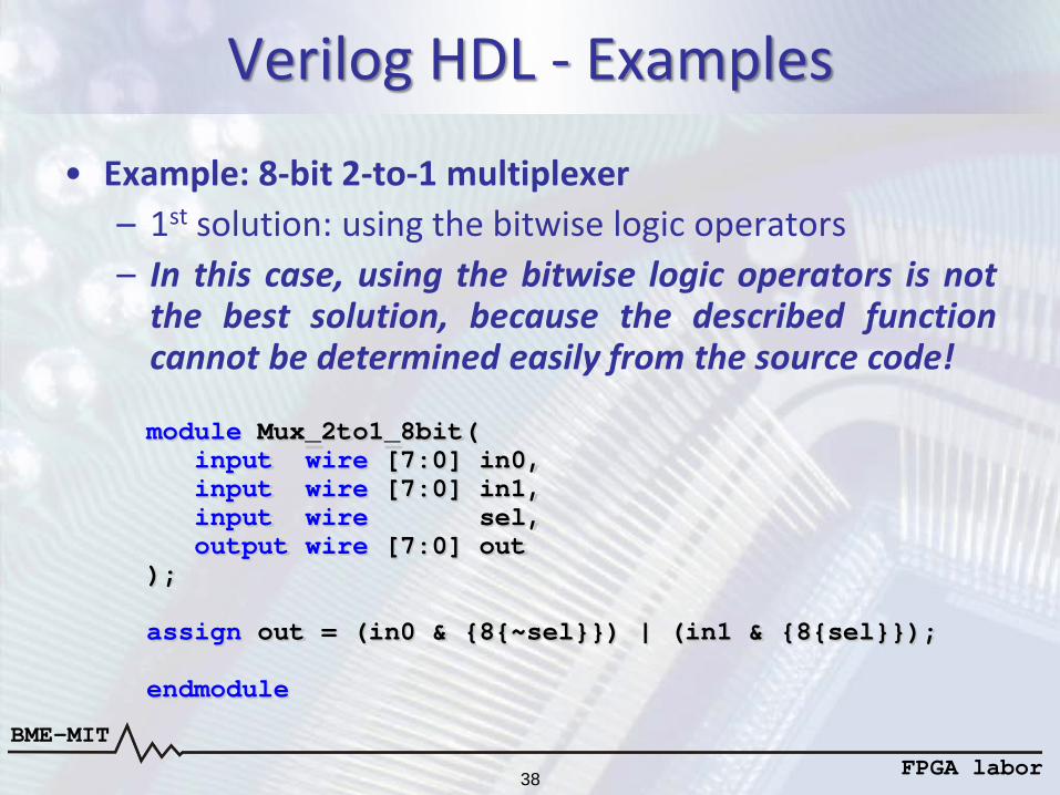
Verilog HDL - Examples
• Example: 8-bit 2-to-1 multiplexer– 1st solution: using the bitwise logic operators– In this case, using the bitwise logic operators is not
the best solution, because the described functioncannot be determined easily from the source code!
module Mux_2to1_8bit(input wire [7:0] in0,input wire [7:0] in1,input wire sel,output wire [7:0] out
);
assign out = (in0 & {8{~sel}}) | (in1 & {8{sel}});
endmodule
38

BME-MITFPGA labor
Verilog HDL - Examples
• Example: 8-bit 2-to-1 multiplexer– 2nd solution:using the conditional operator
module Mux_2to1_8bit(input wire [7:0] in0,input wire [7:0] in1,input wire sel,output wire [7:0] out
);
assign out = (sel) ? in1 : in0;
endmodule
39
BME-MITFPGA labor
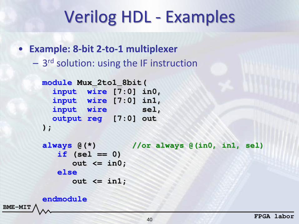
Verilog HDL - Examples
• Example: 8-bit 2-to-1 multiplexer– 3rd solution: using the IF instruction
module Mux_2to1_8bit(input wire [7:0] in0,input wire [7:0] in1,input wire sel,output reg [7:0] out
);
always @(*) //or always @(in0, in1, sel)if (sel == 0)
out <= in0;else
out <= in1;
endmodule
40
BME-MITFPGA labor
Verilog HDL - Examples
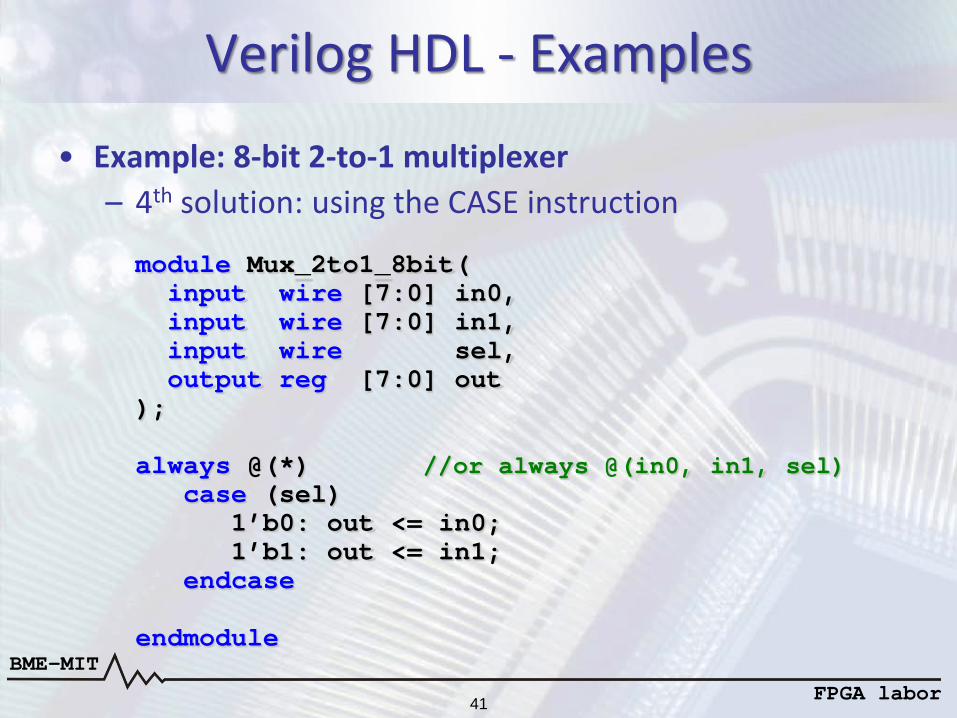
• Example: 8-bit 2-to-1 multiplexer– 4th solution: using the CASE instruction
module Mux_2to1_8bit(input wire [7:0] in0,input wire [7:0] in1,input wire sel,output reg [7:0] out
);
always @(*) //or always @(in0, in1, sel)case (sel)
1’b0: out <= in0;1’b1: out <= in1;
endcase
endmodule
41
BME-MITFPGA labor
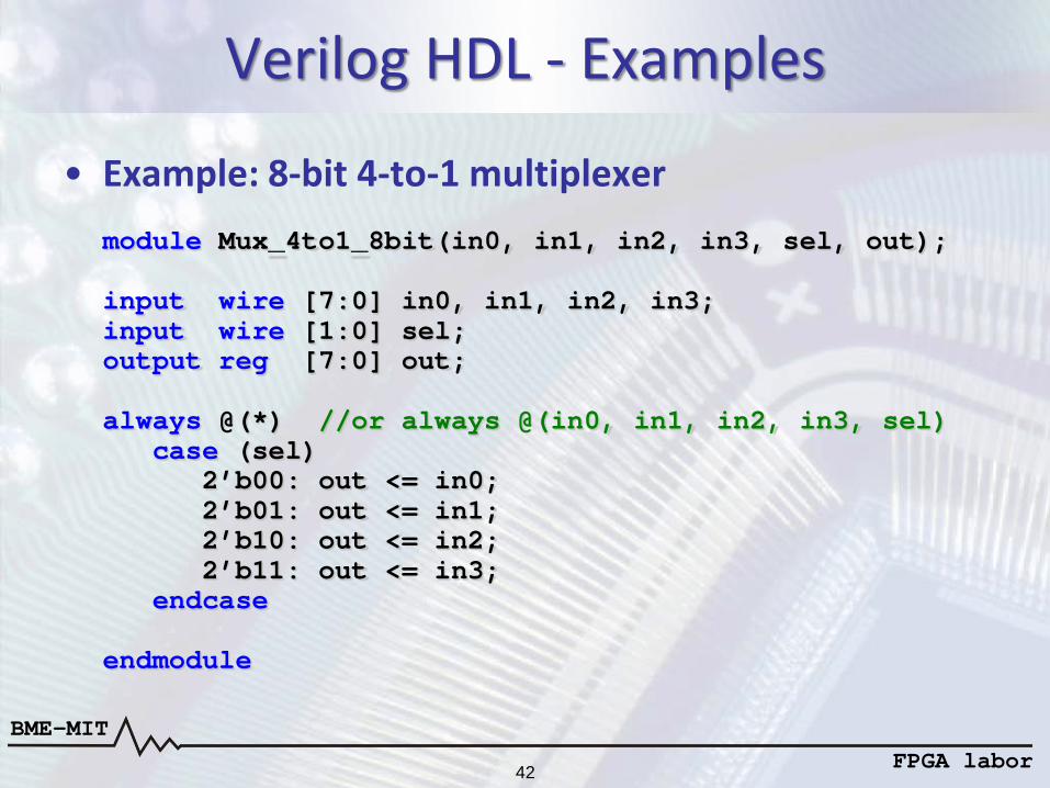
Verilog HDL - Examples
• Example: 8-bit 4-to-1 multiplexermodule Mux_4to1_8bit(in0, in1, in2, in3, sel, out);
input wire [7:0] in0, in1, in2, in3;input wire [1:0] sel;output reg [7:0] out;
always @(*) //or always @(in0, in1, in2, in3, sel)case (sel)
2’b00: out <= in0;2’b01: out <= in1;2’b10: out <= in2;2’b11: out <= in3;
endcase
endmodule
42

BME-MITFPGA labor
Implementing combinational logic
• Wire type signals can implement combinationallogic only
• Reg type signals can implement both combinationaland sequential logic
• When combinational logic is implemented using regtype signals:– The assignment(s) must be evaluated when at
least one input signal is changed:• The sensitivity list of the always block has to contain all
input signals of the combinational logic or a * character• negedge or posedge must not be in the sensitivity list

BME-MITFPGA labor
Implementing combinational logic
• When combinational logic is implemented using regtype signals:– The always blocks must contain only fully specified if
and case instructions– If the if and case instructions are not fully specified,
latches will be inserted (asynchronous flip-flop)• The state of the reg type signal is preserved by the latch
when no assignment is made for the given condition(s)
reg reg_signal;
always @(*)if (sel)
reg_signal <= in0;

BME-MITFPGA labor
Implementing combinational logic
• Latches are undesired, they implement asynchronoussequential logic and not combinational logic
• When the if and case instructions are fully specified(if: all else paths are present, case: all possiblealternatives are listed or the default keyword is used):– The result will be combinational logic (example: MUX)
reg reg_signal;
always @(*)if (sel)
reg_signal <= in1;else
reg_signal <= in0;
BME-MITFPGA labor
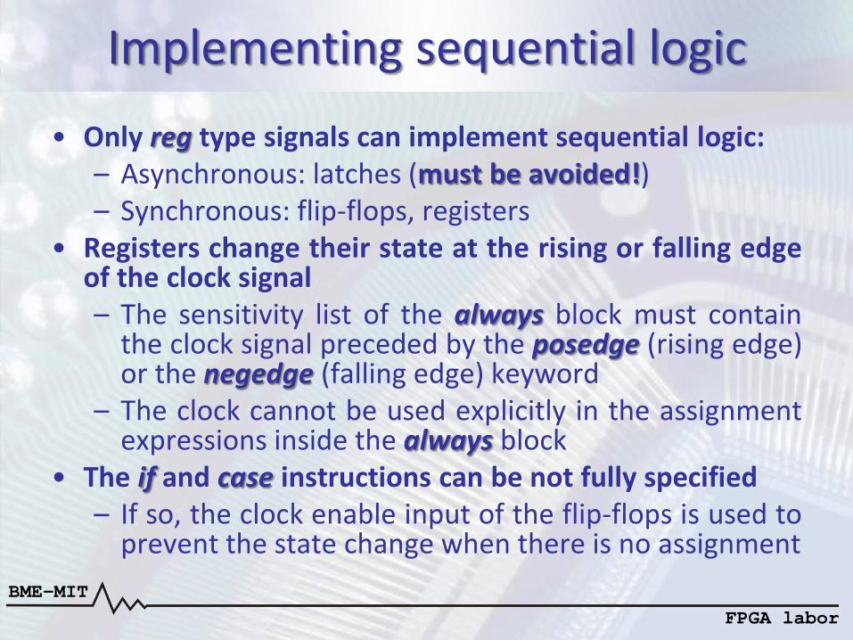
Implementing sequential logic
• Only reg type signals can implement sequential logic:– Asynchronous: latches (must be avoided!)– Synchronous: flip-flops, registers
• Registers change their state at the rising or falling edgeof the clock signal– The sensitivity list of the always block must contain
the clock signal preceded by the posedge (rising edge)or the negedge (falling edge) keyword
– The clock cannot be used explicitly in the assignmentexpressions inside the always block
• The if and case instructions can be not fully specified– If so, the clock enable input of the flip-flops is used to
prevent the state change when there is no assignment

BME-MITFPGA labor
Implementing sequential logic
reg reg_signal;
always @(posedge clk)if (rst)
reg_signal <= 1’b0;else
if (reg_load)reg_signal <= in0;
clock
reset
clock enable
BME-MITFPGA labor
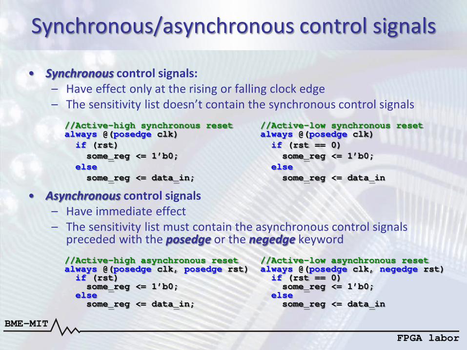
Synchronous/asynchronous control signals
• Synchronous control signals:– Have effect only at the rising or falling clock edge– The sensitivity list doesn’t contain the synchronous control signals
//Active-high synchronous reset //Active-low synchronous resetalways @(posedge clk) always @(posedge clk)
if (rst) if (rst == 0)some_reg <= 1’b0; some_reg <= 1’b0;
else elsesome_reg <= data_in; some_reg <= data_in
• Asynchronous control signals– Have immediate effect– The sensitivity list must contain the asynchronous control signals
preceded with the posedge or the negedge keyword//Active-high asynchronous reset //Active-low asynchronous resetalways @(posedge clk, posedge rst) always @(posedge clk, negedge rst)
if (rst) if (rst == 0)some_reg <= 1’b0; some_reg <= 1’b0;
else elsesome_reg <= data_in; some_reg <= data_in

BME-MITFPGA labor
Finite state machines (FSMs)• Local parameters can be used to define the states• A register is required to store the current state• The case instruction can be used to select the current state
– In each alternative, the if or case instructions can be used to check the value of the inputs and execute the proper state transition
• Example: traffic light controller– 4 states: red, red-yellow, green, yellow– An external timer generates the 1 clock cycle long enable signal
Traffic light controller FSM
CLK ENABLE
Timer
CLK
CLK
r
y
g
BME-MITFPGA labor
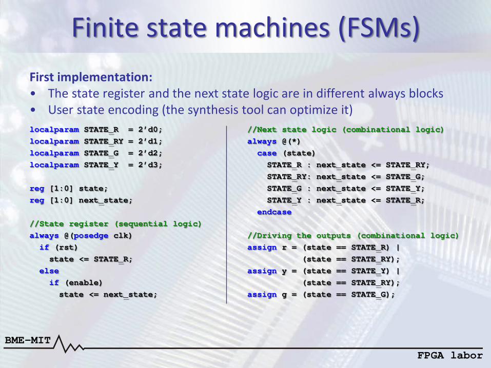
Finite state machines (FSMs)First implementation:• The state register and the next state logic are in different always blocks• User state encoding (the synthesis tool can optimize it)localparam STATE_R = 2’d0;localparam STATE_RY = 2’d1;localparam STATE_G = 2’d2;localparam STATE_Y = 2’d3;
reg [1:0] state;reg [1:0] next_state;
//State register (sequential logic)always @(posedge clk)if (rst)
state <= STATE_R;else
if (enable)state <= next_state;
//Next state logic (combinational logic)always @(*)case (state)
STATE_R : next_state <= STATE_RY;STATE_RY: next_state <= STATE_G;STATE_G : next_state <= STATE_Y;STATE_Y : next_state <= STATE_R;
endcase
//Driving the outputs (combinational logic)assign r = (state == STATE_R) |
(state == STATE_RY);assign y = (state == STATE_Y) |
(state == STATE_RY);assign g = (state == STATE_G);

BME-MITFPGA labor
Finite state machines (FSMs)Second implementation:• The state register and the next state logic are in the same always block• User state encoding (the synthesis tool can optimize it)localparam STATE_R = 2’d0;localparam STATE_RY = 2’d1;localparam STATE_G = 2’d2;localparam STATE_Y = 2’d3;
reg [1:0] state;
//State register and the next state logicalways @(posedge clk)begin
if (rst)state <= STATE_R;
elsecase (state)STATE_R : if (enable)
state <= STATE_RY;elsestate <= STATE_R;
STATE_RY: if (enable)state <= STATE_G;
elsestate <= STATE_RY;
STATE_G : if (enable)state <= STATE_Y;
elsestate <= STATE_G;
STATE_Y : if (enable)state <= STATE_R;
elsestate <= STATE_Y;
endcaseend
//Driving the outputs (combinational logic)assign r = (state==STATE_R) | (state==STATE_RY);assign y = (state==STATE_Y) | (state==STATE_RY);assign g = (state==STATE_G);

BME-MITFPGA labor
Finite state machines (FSMs)Third implementation:• The state register and the next state logic are in different always blocks• Output encoding: the (* fsm_encoding = ”user” *) Xilinx-specific Verilog
directive disables the state encoding optimization for the state registerlocalparam STATE_R = 3’b100;localparam STATE_RY = 3’b110;localparam STATE_G = 3’b001;localparam STATE_Y = 3’b010;
(* fsm_encoding = ”user” *)reg [2:0] state;reg [2:0] next_state;
//State register (sequential logic)always @(posedge clk)if (rst)
state <= STATE_R;else
if (enable)state <= next_state;
//Next state logic (combinational logic)always @(*)case (state)
STATE_R : next_state <= STATE_RY;STATE_RY: next_state <= STATE_G;STATE_G : next_state <= STATE_Y;STATE_Y : next_state <= STATE_R;
endcase
//Driving the outputsassign r = state[2];assign y = state[1];assign g = state[0];
BME-MITFPGA labor
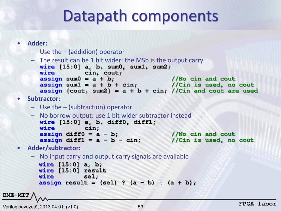
Datapath components• Adder:
– Use the + (addidion) operator– The result can be 1 bit wider: the MSb is the output carry
wire [15:0] a, b, sum0, sum1, sum2;wire cin, cout;assign sum0 = a + b; //No cin and coutassign sum1 = a + b + cin; //Cin is used, no coutassign {cout, sum2} = a + b + cin; //Cin and cout are used
• Subtractor: – Use the – (subtraction) operator– No borrow output: use 1 bit wider subtractor instead
wire [15:0] a, b, diff0, diff1;wire cin;assign diff0 = a – b; //No cin and coutassign diff1 = a – b - cin; //Cin is used, no cout
• Adder/subtractor:– No input carry and output carry signals are available
wire [15:0] a, b;wire [15:0] resultwire sel;assign result = (sel) ? (a – b) : (a + b);
Verilog bevezető, 2013.04.01. (v1.0) 53
BME-MITFPGA labor
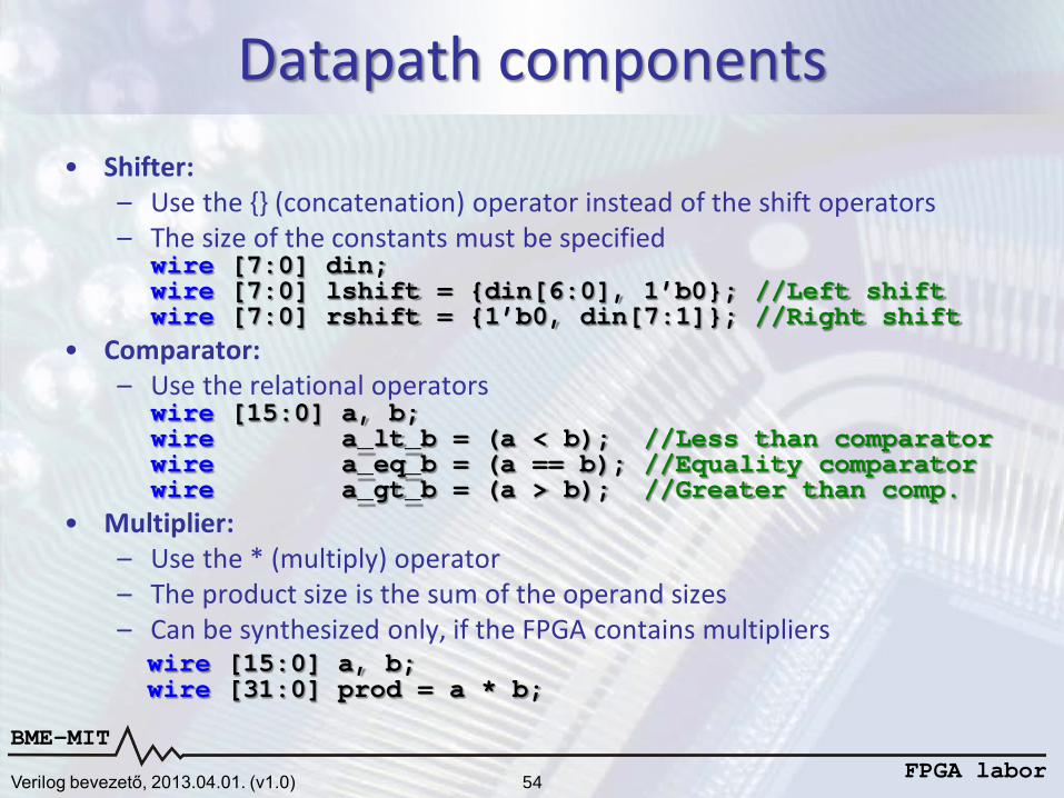
Datapath components• Shifter:
– Use the {} (concatenation) operator instead of the shift operators– The size of the constants must be specified
wire [7:0] din;wire [7:0] lshift = {din[6:0], 1’b0}; //Left shiftwire [7:0] rshift = {1’b0, din[7:1]}; //Right shift
• Comparator: – Use the relational operators
wire [15:0] a, b;wire a_lt_b = (a < b); //Less than comparatorwire a_eq_b = (a == b); //Equality comparatorwire a_gt_b = (a > b); //Greater than comp.
• Multiplier:– Use the * (multiply) operator– The product size is the sum of the operand sizes– Can be synthesized only, if the FPGA contains multiplierswire [15:0] a, b;wire [31:0] prod = a * b;
Verilog bevezető, 2013.04.01. (v1.0) 54

BME-MITFPGA labor
Datapath components• Shift register (example):
– Synchronous reset and load– Bi-directional: can shift left and right
reg [7:0] shr;wire [7:0] din;wire rst, load, dir, serin;
always @(posedge clk)if (rst)
shr <= 8’d0; //Resetelse
if (load)shr <= din; //Load
elseif (dir)shr <= {serin, shr[7:1]}; //Right shift
elseshr <= {shr[6:0], serin}; //Left shift
Verilog bevezető, 2013.04.01. (v1.0) 55
BME-MITFPGA labor
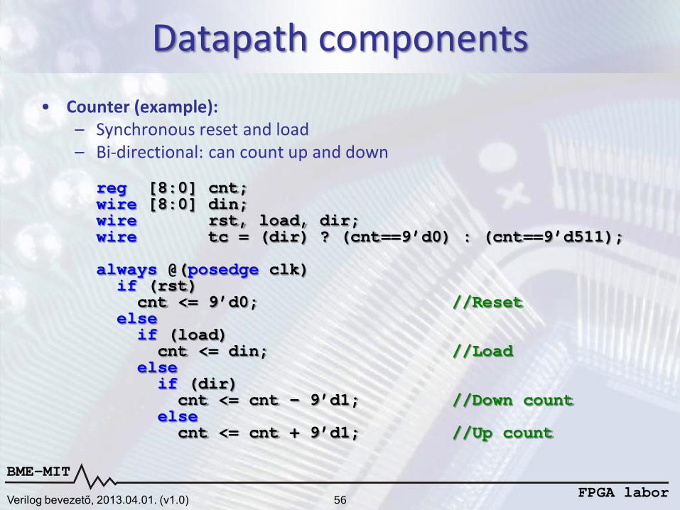
Datapath components• Counter (example):
– Synchronous reset and load– Bi-directional: can count up and down
reg [8:0] cnt;wire [8:0] din;wire rst, load, dir;wire tc = (dir) ? (cnt==9’d0) : (cnt==9’d511);
always @(posedge clk)if (rst)
cnt <= 9’d0; //Resetelse
if (load)cnt <= din; //Load
elseif (dir)cnt <= cnt – 9’d1; //Down count
elsecnt <= cnt + 9’d1; //Up count
Verilog bevezető, 2013.04.01. (v1.0) 56

BME-MITFPGA labor
Datapath components(Priority of the control signals)
The value of the control inputs are examined in the orderthey are listed inside the always blocks (nested ifinstructions)always @(posedge clk) always @(posedge clk) always @(posedge clk)
if (rst) if (rst) if (en)cnt <= 9’d0; cnt <= 9’d0; if (clr)
else else cnt <= 9’d0;if (load) if (en) elsecnt <= data_in; if (load) if (load)
else cnt <= data_in; cnt <= data_in;if (en) else elsecnt <= cnt + 9’d1; cnt <= cnt + 9’d1; cnt <= cnt + 9’d1;
rst load en Operation
1 x x Reset
0 1 x Load
0 0 1 Up count
0 0 0 No change
Verilog bevezető, 2013.04.01. (v1.0) 57
rst en load Operation
1 x x Reset
0 1 1 Load
0 1 0 Up count
0 0 x No change
en clr load Operation
0 x x No change
1 1 x Clear
1 0 1 Load
1 0 0 Up count