diffusion xidation and ion implantationnewagepublishers.com/samplechapter/001946.pdf · chapter 6...
TRANSCRIPT
CH
AP
TE
R6DIFFUSION, OXIDATION AND ION IMPLANTATION
This chapter will discuss some important processing techniques for device fabrication. These have beendiscussed earlier by Ghandy [1] and Sze [2]. The present chapter introduces some newer techniquessuch as laser annealing and presents some new research results on GaAs. While Diffusion and Oxida-tion are particularly important for Silicon-based devices, Ion Implantation is the preferred technique forall semiconductor devices including III-V and II-VI compounds, since all semiconductor devices re-quire a desired doping concentration and doping profile for optimum performance.
In the fifties doping was carried out during crystal growth and simple p-n junctions could thus bemade. In amorphous Si devices doping is still carried out during deposition as discussed in Ch 4.Nowadays however the bulk single crystal wafer forms a high quality substrate for further processing,which could include epitaxial growth followed by ion implantation. Till the seventies doping in Si wascarried out using high temperature diffusion. Since then ion implantation has become the workhorseespecially for shallow doping. Diffusion is still employed for deep junctions and a combination of the2 processes may be used. Since the implantation of high energy ions results in damage to the crystallinelattice, this must be followed by annealing in a furnace or by lamps as in a rapid thermal anneal (RTA)process.
6.1 DIFFUSION
Diffusion is a process that involves the motion of atoms through a solid and is driven by a concentrationgradient. In crystalline semiconductors the motion of impurity atoms occurs by
(a) substitutional(b) interstitial(c) substitutional-cum-interstitial mechanisms or(d) direct exchange and cooperative exchange.
These are shown schematically in Fig. 6.1. For substitutional diffusion there must exist a concen-tration of vacancies to which the impurity or host atom can jump. For interstitial diffusion the presenceof vacancies is not absolutely necessary while in the third case the impurity can move occupying bothsubstitutional and interstitial sites. Direct exchange and cooperative exchange have low probabilitiesand are not considered further.

358 SEMICONDUCTOR MATERIALS & DEVICES
Fig. 6.1 Diffusion mechanisms: (a) substitutional (b) interstitial (c) substitutional-cum-interstitial(d) direct exchange and cooperative exchange
6.2 FICK’S FIRST LAW
Atoms in a lattice in thermal equilibrium can be considered to vibrate about their lattice positions. Withincrease in temperature these may acquire enough energy to overcome the potential barriers and thusjump to adjacent substitutional or interstitial sites. In the presence of a concentration gradient, moreimpurity atoms will jump in the direction of the gradient and than in the opposite direction and henceconstitute a flux of diffusing atoms. Thus diffusion is governed by Fick’s First law which states that theflux F per unit area per unit time is proportional to the diffusion coefficient and the concentrationgradient:
dCF D
dx= − ...(6.1)
where C = dopant concentration per unit volume. This is Fick’s law in one dimension. The negative signindicates that the flux is from high to low doping concentration. The diffusion coefficient D depends onthe type of individual atom and is strongly dependent on temperature being given by
D = D0 exp (−Ea/kT) ...(6.2)
(a) (b)
12
34
1
2 3
4 5
6
(c) (d)
DIFFUSION, OXIDATION AND ION IMPLANTATION 359
where D0 = diffusion coefficient extrapolated to infinite temperature in units of cm2/s and Ea = activa-tion energy in eV.
One of the standard methods for determining diffusion coefficients is by the radioactive tracertechnique. In this a radioactive species is coated on one end of a sample and diffused at a high tempera-ture for a given time. The sample is then taken out and sliced into sections. The radioactive counts forthe different sections are then measured and the diffusion profile thus determined and fitted with agaussian or error function profile as determined by the diffusion condition. The experiment has to berepeated over a range of temperatures to find D0 and Ea.
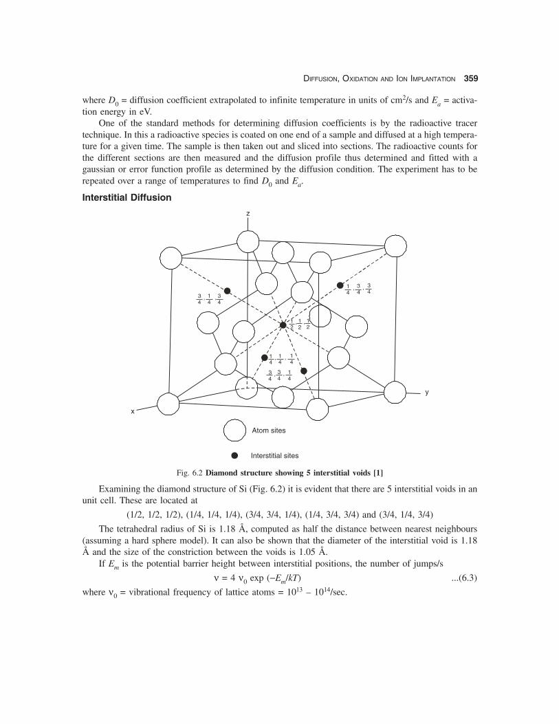
Interstitial Diffusion
Fig. 6.2 Diamond structure showing 5 interstitial voids [1]
Examining the diamond structure of Si (Fig. 6.2) it is evident that there are 5 interstitial voids in anunit cell. These are located at
(1/2, 1/2, 1/2), (1/4, 1/4, 1/4), (3/4, 3/4, 1/4), (1/4, 3/4, 3/4) and (3/4, 1/4, 3/4)
The tetrahedral radius of Si is 1.18 Å, computed as half the distance between nearest neighbours(assuming a hard sphere model). It can also be shown that the diameter of the interstitial void is 1.18Å and the size of the constriction between the voids is 1.05 Å.
If Em is the potential barrier height between interstitial positions, the number of jumps/s
ν = 4 ν0 exp (−Em/kT) ...(6.3)
where ν0 = vibrational frequency of lattice atoms = 1013 – 1014/sec.
x
y
z
14
34
, ,
14
, 14
, 14
, , 14
14
,,
Atom sites
Interstitial sites
12
, 12
, 12
360 SEMICONDUCTOR MATERIALS & DEVICES
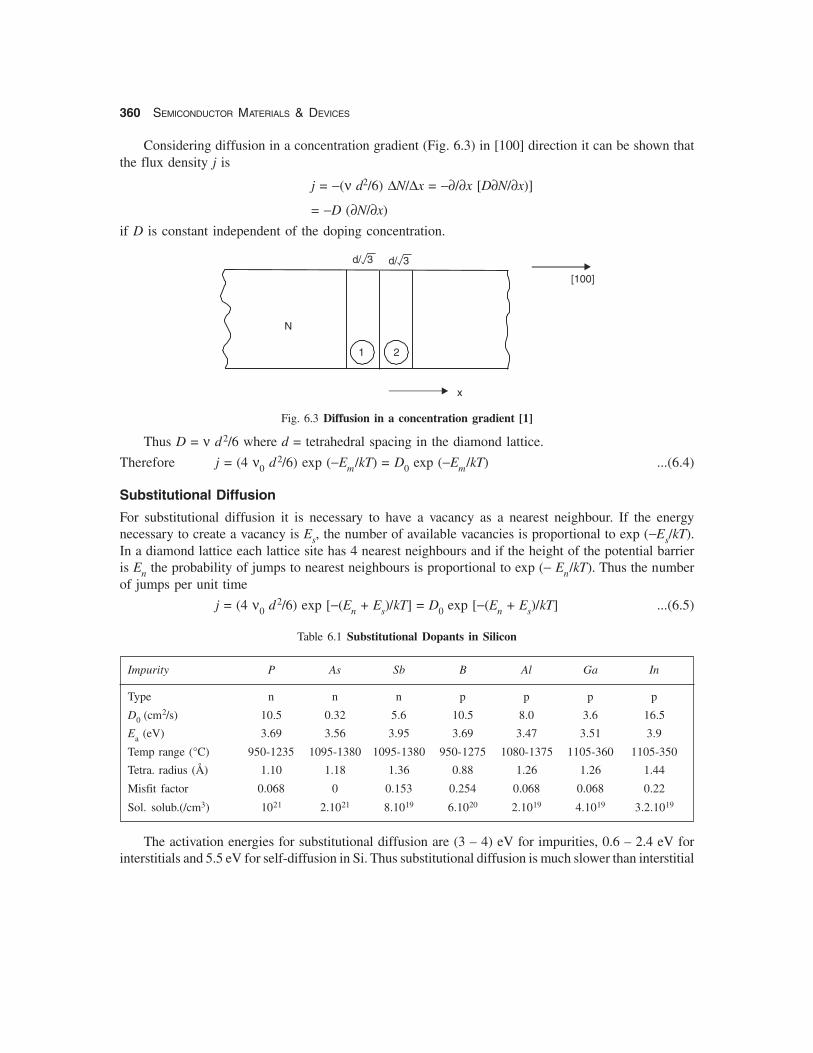
Considering diffusion in a concentration gradient (Fig. 6.3) in [100] direction it can be shown thatthe flux density j is
j = −(ν d2/6) ΔN/Δx = −∂/∂x [D∂N/∂x)]
= −D (∂N/∂x)
if D is constant independent of the doping concentration.
Fig. 6.3 Diffusion in a concentration gradient [1]
Thus D = ν d2/6 where d = tetrahedral spacing in the diamond lattice.
Therefore j = (4 ν0 d2/6) exp (−Em/kT) = D0 exp (−Em/kT) ...(6.4)
Substitutional Diffusion
For substitutional diffusion it is necessary to have a vacancy as a nearest neighbour. If the energynecessary to create a vacancy is Es, the number of available vacancies is proportional to exp (−Es/kT).In a diamond lattice each lattice site has 4 nearest neighbours and if the height of the potential barrieris En the probability of jumps to nearest neighbours is proportional to exp (− En/kT). Thus the numberof jumps per unit time
j = (4 ν0 d2/6) exp [−(En + Es)/kT] = D0 exp [−(En + Es)/kT] ...(6.5)
Table 6.1 Substitutional Dopants in Silicon
Impurity P As Sb B Al Ga In
Type n n n p p p p
D0 (cm2/s) 10.5 0.32 5.6 10.5 8.0 3.6 16.5
Ea (eV) 3.69 3.56 3.95 3.69 3.47 3.51 3.9
Temp range (°C) 950-1235 1095-1380 1095-1380 950-1275 1080-1375 1105-360 1105-350
Tetra. radius (Å) 1.10 1.18 1.36 0.88 1.26 1.26 1.44
Misfit factor 0.068 0 0.153 0.254 0.068 0.068 0.22
Sol. solub.(/cm3) 1021 2.1021 8.1019 6.1020 2.1019 4.1019 3.2.1019
The activation energies for substitutional diffusion are (3 – 4) eV for impurities, 0.6 – 2.4 eV forinterstitials and 5.5 eV for self-diffusion in Si. Thus substitutional diffusion is much slower than interstitial
N
x
[100]
d/ 3
21
d/ 3
DIFFUSION, OXIDATION AND ION IMPLANTATION 361
diffusion and requires higher temperatures and longer times. The variation of D vs 1000/T for impuritiesin Si is shown in Fig. 6.4(a).
The substitutional impurities belonging to Groups III & V are the ones used for doping since thesegive rise to shallow acceptors and donors respectively. These single-charged donors are positivelycharged while acceptors are negatively charged when ionized.
Impurity – Vacancy Interactions
The process of diffusion of substitutional impurities involves interaction with vacancies which can havevarious charge states such as V+, V°, V−, V2− etc. These impurity atoms will interact with vacanciesdepending on their charge state and each I-V combination will have its own activation energy. Thuscorresponding to each I − V+, I − V° , I − V− , I − V2− pair there will be intrinsic diffusion coefficients
D D D Di i i i+ − −, , ,0 2 etc. Thus the overall intrinsic diffusivity will be given by
D D D D Di i i i i= + + ++ − −0 2
For the case of extrinsic diffusion the variation of the Fermi level with doping has to be taken intoaccount as discussed by Ghandy [1]. This also affects the population of different charged vacancies. Sivacancies exhibit the charge states V+, V− and V2− with locations in the energy band gap at EV + (0.06– 0.16) eV, EC – 0.44 eV and EC – 0.11 eV respectively. Thus diffusing acceptors have only I − V+ typeinteractions while donors interact with negatively charged species I − V− and I − V2−.
Choice of n-type impurities in Silicon
Impurity Diffusion coefficient Energy level CommentsED (eV)
P High-same as B 0.044 Short diffusion time, shallow donorMost widely used
As Low 0.049 Slow diffuser - first diffusion;Shallow donor. Small misfit factor –Highest solubility. Toxic
Sb Low-high EA 0.039 Slow diffuser - Shallow donor.Preferred to As as less toxic.
Choice of p-type impurities in Silicon
Impurity Diffusion coefficient Energy level CommentsEA (eV)
B High-same as P 0.045 Short diffusion time, shallow donorHighest solubility; Most widely used
Al Moderate 0.065 Highly reactive with O – not commonly used
Ga Moderate 0.065 Highly diffusion coefficient in SiO2;Used only for high power diodes
In Slow diffuser; low 0.16 Deep acceptor partly ionized at 300K;solubility used as 7–8 μm IR detector
362 SEMICONDUCTOR MATERIALS & DEVICES
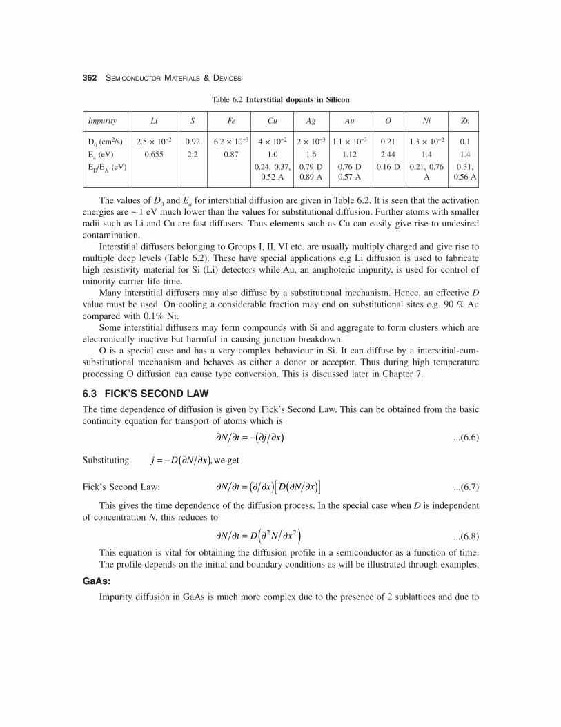
Table 6.2 Interstitial dopants in Silicon
Impurity Li S Fe Cu Ag Au O Ni Zn
D0 (cm2/s) 2.5 × 10⁻² 0.92 6.2 × 10⁻³ 4 × 10⁻² 2 × 10⁻³ 1.1 × 10⁻³ 0.21 1.3 × 10⁻² 0.1
Ea (eV) 0.655 2.2 0.87 1.0 1.6 1.12 2.44 1.4 1.4
ED/EA (eV) 0.24, 0.37, 0.79 D 0.76 D 0.16 D 0.21, 0.76 0.31,0.52 A 0.89 A 0.57 A A 0.56 A
The values of D0 and Ea for interstitial diffusion are given in Table 6.2. It is seen that the activationenergies are ~ 1 eV much lower than the values for substitutional diffusion. Further atoms with smallerradii such as Li and Cu are fast diffusers. Thus elements such as Cu can easily give rise to undesiredcontamination.
Interstitial diffusers belonging to Groups I, II, VI etc. are usually multiply charged and give rise tomultiple deep levels (Table 6.2). These have special applications e.g Li diffusion is used to fabricatehigh resistivity material for Si (Li) detectors while Au, an amphoteric impurity, is used for control ofminority carrier life-time.
Many interstitial diffusers may also diffuse by a substitutional mechanism. Hence, an effective Dvalue must be used. On cooling a considerable fraction may end on substitutional sites e.g. 90 % Aucompared with 0.1% Ni.
Some interstitial diffusers may form compounds with Si and aggregate to form clusters which areelectronically inactive but harmful in causing junction breakdown.
O is a special case and has a very complex behaviour in Si. It can diffuse by a interstitial-cum-substitutional mechanism and behaves as either a donor or acceptor. Thus during high temperatureprocessing O diffusion can cause type conversion. This is discussed later in Chapter 7.
6.3 FICK’S SECOND LAW
The time dependence of diffusion is given by Fick’s Second Law. This can be obtained from the basiccontinuity equation for transport of atoms which is
∂ ∂ ∂ ∂N t j x= −b g ...(6.6)
Substituting j D N x= − ∂ ∂b g,we get
Fick’s Second Law: ∂ ∂ ∂ ∂ ∂ ∂N t x D N x= b g b g ...(6.7)
This gives the time dependence of the diffusion process. In the special case when D is independentof concentration N, this reduces to
∂ ∂ ∂ ∂N t D N x= 2 2e j ...(6.8)
This equation is vital for obtaining the diffusion profile in a semiconductor as a function of time.The profile depends on the initial and boundary conditions as will be illustrated through examples.
GaAs:
Impurity diffusion in GaAs is much more complex due to the presence of 2 sublattices and due to
DIFFUSION, OXIDATION AND ION IMPLANTATION 363
the varied types of defects that are present. Since VAs and VGa are both neutral, Deff depends only in 0.iD
The high As vapour pressure also results in the presence of As vacancies.It is thought that n-type impurities from Group VI such as S, Se and Te move along the As sublattice
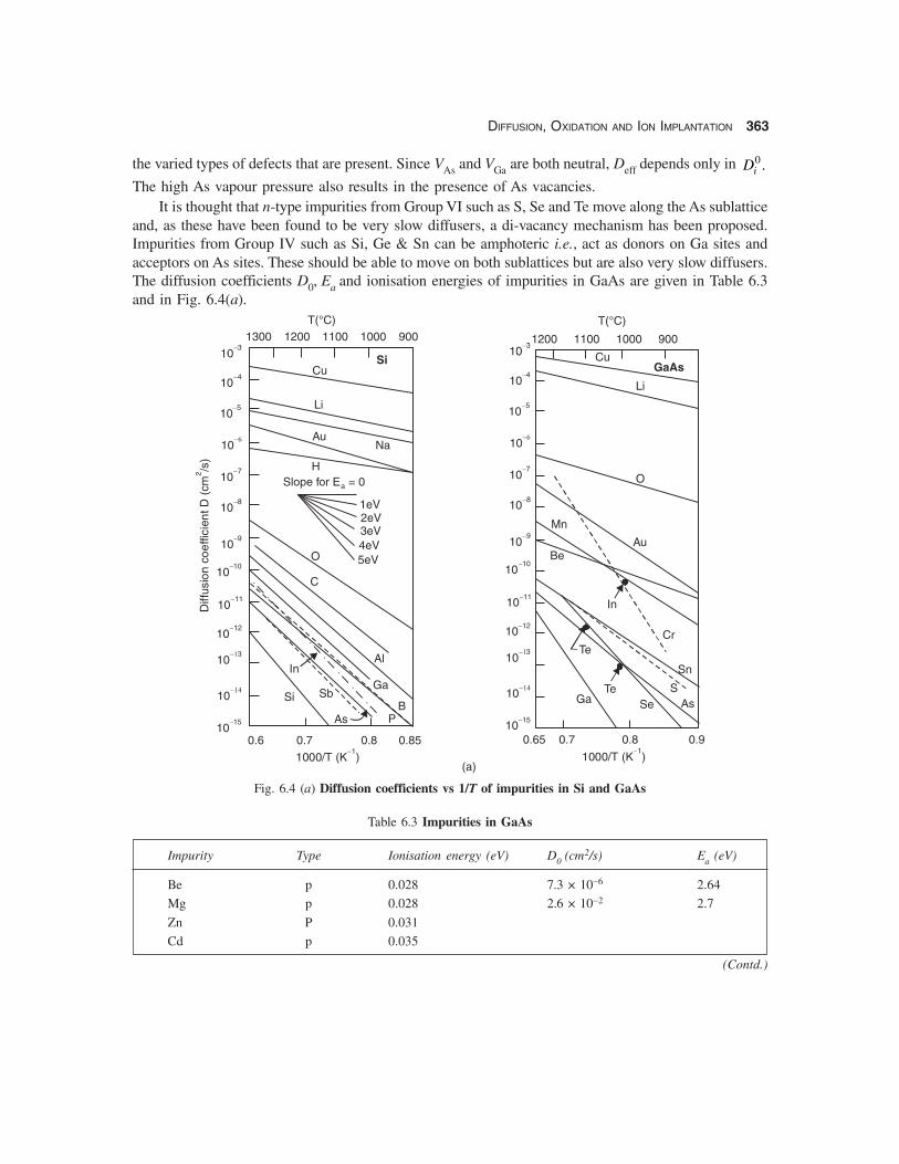
and, as these have been found to be very slow diffusers, a di-vacancy mechanism has been proposed.Impurities from Group IV such as Si, Ge & Sn can be amphoteric i.e., act as donors on Ga sites andacceptors on As sites. These should be able to move on both sublattices but are also very slow diffusers.The diffusion coefficients D0, Ea and ionisation energies of impurities in GaAs are given in Table 6.3and in Fig. 6.4(a).
Fig. 6.4 (a) Diffusion coefficients vs 1/T of impurities in Si and GaAs
Table 6.3 Impurities in GaAs
Impurity Type Ionisation energy (eV) D0 (cm2/s) Ea (eV)
Be p 0.028 7.3 × 10⁻⁶ 2.64
Mg p 0.028 2.6 × 10⁻² 2.7
Zn P 0.031
Cd p 0.035
(Contd.)
1200 1100 1000 900
0.65 0.7 0.8 0.9
Cu
Li
Au
O
Mn
Be
In
CrTe
Sn
STeSe As
T(°C)
1000/T (K )�1
GaAs
1300 1200 1100 1000 900
0.6 0.7 0.8 0.85
10�4 10
�4
10�5 10
�5
10�� 10
��
10�7 10
�7
10�8 10
�8
10�9 10
�9
10�10 10
�10
10�11 10
�11
10�12 10
�12
10��3 10
��3
10��� 10
���
10�15 10
�15
Si
Cu
Li
AuNa
H
O
C
AlIn
Ga
Si
SbB
PAs
1eV2eV3eV4eV5eV
Slope for E = 0a
T(°C)
Diff
usio
nco
effic
ient
D(c
m/s
)2
1000/T (K )�1
(a)
Ga
364 SEMICONDUCTOR MATERIALS & DEVICES
Impurity Type Ionisation energy (eV) D0 (cm2/s) Ea (eV)
C n/p 0.006(D); 0.026(A)
Si n/p 0.0058(D); 0.035(A)
Ge n/p 0.006(D),.07,.04 (A)
Sn n/p 0.006 (D); 0.17(A) 3.8 × 10⁻² 2.7
Se n 0.006 3.0 × 10³ 4.16
Te N 0.03 D = 10−13 @ 1000° C
Au P 0.09 2.9 × 101 2.64
Cr deep 0.63 (A) 4.3 × 10³ 3.4
Cu deep multiple 3 × 10⁻² 0.53
Mn p 0.095 6.5 × 10⁻¹ 2.49
O deep 0.40(D), 0.67(D) 2 × 10⁻² 1.1
Li deep 5/3 × 10−1 1.0
P-type dopants from Group II such as Be, Mg, Zn, Cd and Hg move in the Ga sublattice.Only Zn diffusion, used for the formation of shallow p-type layers and p-n junctions, has been
studied in detail. Zn is a fast diffuser and moves by an interstitial-substitutional mechanism exhibitingdependence on carrier concentration. Since the intrinsic carrier concentration of GaAs at 1000° C is lessthan 1018/cm3 even for the lowest surface concentration of Zn, the diffusion is in the extrinsic region andhence is concentration dependent.
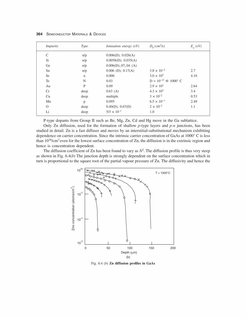
The diffusion coefficient of Zn has been found to vary as N2. The diffusion profile is thus very steepas shown in Fig. 6.4(b) The junction depth is strongly dependent on the surface concentration which inturn is proportional to the square root of the partial vapour pressure of Zn. The diffusivity and hence the
Fig. 6.4 (b) Zn diffusion profiles in GaAs
1020
10��
10��
1017
0 50 100 150 200
T = 1000°C
Depth ( m)�
Zin
cco
ncen
trat
ion
(ato
ms/
cm)3
(b)
DIFFUSION, OXIDATION AND ION IMPLANTATION 365
junction depth is thus linearly proportional to the surface concentration. Relatively low temperatures(600 – 800°C) suffice for the formation of p-n junctions using Zn but render control rather difficult. Cdon the other hand is a much slower diffuser and hence capable of good control over junction depth.
Hg Cd Te MCT1 x x-
a f
As a II-VI compound, group III and VII elements act as donors while Group I and V elements areexpected to behave as acceptors in MCT. Si is found to behave as a donor on Group II site. In additiondue to low defect formation energies, native defects play an important role VHg acting as acceptor andVTe as donor. The diffusivity of impurities in MCT are given in the Table 6.4
Table 6.4 Behaviour of Dopants in Hg1−x
CdxTe
Element Type Diffusion
Ga Donor FastIn Donor FastAg Acceptor FastCu Acceptor FastAu Acceptor FastLi Acceptor FastAl Donor SlowSi Donor SlowP Acceptor SlowAs Acceptor SlowBr Donor Slow
6.4 DIFFUSION PROFILES
For device fabrication it is important to be able to tailor diffusion profiles according to requirements.The profiles depend on the initial and boundary conditions. The two most important conditions areConstant Source and Instantaneous Source Diffusion. In the first case the silicon wafer surface isexposed to an impurity source of constant concentration for the entire diffusion period while in thesecond case a fixed amount of dopant is deposited on the semiconductor surface and is subsequentlydiffused into the wafer.
(a) Constant Source Diffusion
In Fig. 6.5(a) the initial condition is N(x, 0) = 0 since the dopant concentration on the surface is initiallyzero.
The boundary conditions are
N (0, t) = N0 and N (∝, t) = 0 ...(6.9)
where N0 = the surface concentration which is constant independent of time. The second boundarycondition states that at large distances from the surface the impurity concentration is zero.
Inserting these conditions into Fick’s second equation and solving (see Appendix 6.1 given at theend) the doping profile obtained is
N (x, t) = N0 erfc [x/2 (Dt)1/2] ...(6.10)
366 SEMICONDUCTOR MATERIALS & DEVICES
where D = diffusion coefficient, t = time of diffusion and erfc = 1 – erf so that
( ) ( )( )
( )2 1 2
1 2 1 2 2
0
2 1 2 expx D t
erfc x Dt z dzp
⎡ ⎤⎡ ⎤ ⎢ ⎥= − −⎢ ⎥⎣ ⎦ ⎢ ⎥
⎣ ⎦∫ ...(6.11)
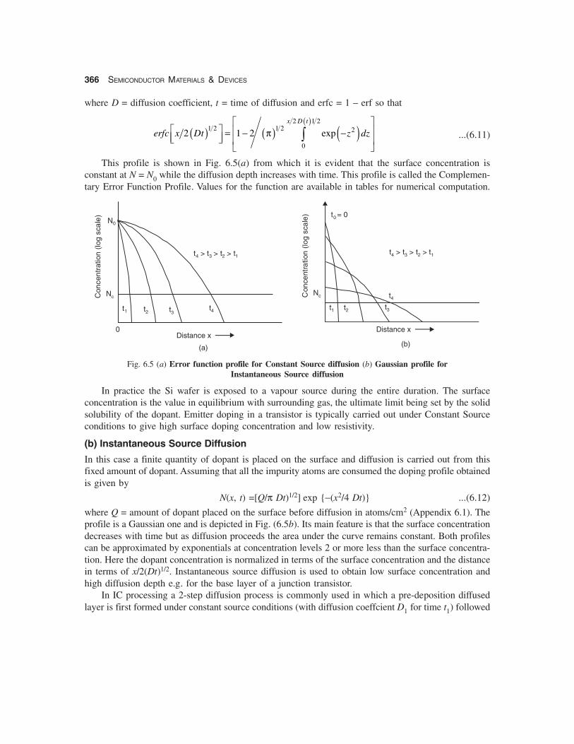
This profile is shown in Fig. 6.5(a) from which it is evident that the surface concentration isconstant at N = N0 while the diffusion depth increases with time. This profile is called the Complemen-tary Error Function Profile. Values for the function are available in tables for numerical computation.
Fig. 6.5 (a) Error function profile for Constant Source diffusion (b) Gaussian profile forInstantaneous Source diffusion
In practice the Si wafer is exposed to a vapour source during the entire duration. The surfaceconcentration is the value in equilibrium with surrounding gas, the ultimate limit being set by the solidsolubility of the dopant. Emitter doping in a transistor is typically carried out under Constant Sourceconditions to give high surface doping concentration and low resistivity.
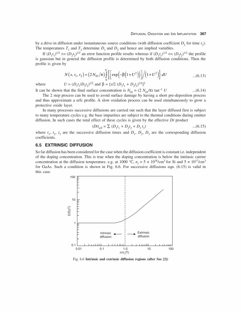
(b) Instantaneous Source Diffusion
In this case a finite quantity of dopant is placed on the surface and diffusion is carried out from thisfixed amount of dopant. Assuming that all the impurity atoms are consumed the doping profile obtainedis given by
N(x, t) =[Q/π Dt)1/2] exp {−(x2/4 Dt)} ...(6.12)
where Q = amount of dopant placed on the surface before diffusion in atoms/cm2 (Appendix 6.1). Theprofile is a Gaussian one and is depicted in Fig. (6.5b). Its main feature is that the surface concentrationdecreases with time but as diffusion proceeds the area under the curve remains constant. Both profilescan be approximated by exponentials at concentration levels 2 or more less than the surface concentra-tion. Here the dopant concentration is normalized in terms of the surface concentration and the distancein terms of x/2(Dt)1/2. Instantaneous source diffusion is used to obtain low surface concentration andhigh diffusion depth e.g. for the base layer of a junction transistor.
In IC processing a 2-step diffusion process is commonly used in which a pre-deposition diffusedlayer is first formed under constant source conditions (with diffusion coeffcient D1 for time t1) followed
N0
Nc
t4 > t3 > t2 > t1
t1 t2 t3 t4
0
Con
cent
ratio
n(lo
gsc
ale)
Distance x
t = 00
Nc
t4 > t3 > t2 > t1
t1 t2 t3
t4Con
cent
ratio
n(lo
gsc
ale)
Distance x
(a) (b)
DIFFUSION, OXIDATION AND ION IMPLANTATION 367
by a drive-in diffusion under instantaneous source conditions (with diffusion coeffcient D2 for time t2).The temperatures T1 and T2 determine D1 and D2 and hence are implied variables.
If (D1t1)1/2 >> (D2t2)
1/2 an error function profile results whereas if (D1t1)1/2 << (D2t2)
1/2 the profileis gaussian but in general the diffusion profile is determined by both diffusion conditions. Then theprofile is given by
( ) ( ) ( )( ) ( ){ }2 21 2 01
0
, , 2 exp 1 1U
N x t t N U U dUp b⎡ ⎤= − + +⎢ ⎥⎣ ⎦∫ ...(6.13)
where U = (D1t1/D2t2)1/2 and β = [x/2 (D1t1 + D2t2)1/2]2
It can be shown that the final surface concentration is N02 = (2 N01/π) tan−1 U ...(6.14)The 2 step process can be used to avoid surface damage by having a short pre-deposition process
and thus approximate a erfc profile. A slow oxidation process can be used simultaneously to grow aprotective oxide layer.
In many processes successive diffusions are carried out such that the layer diffused first is subjectto many temperature cycles e.g. the base impurities are subject to the thermal conditions during emitterdiffusion. In such cases the total effect of these cycles is given by the effective Dt product
(Dt)eff = ∑ (D1t1 + D2t2 + D3 t3) ...(6.15)
where t1, t2, t3 are the successive diffusion times and D1, D2, D3 are the corresponding diffusioncoefficients.
6.5 EXTRINSIC DIFFUSION
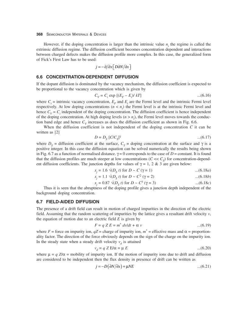
So far diffusion has been considered for the case when the diffusion coefficient is constant i.e. independentof the doping concentration. This is true when the doping concentration is below the intrinsic carrierconcentration at the diffusion temperature. e.g. at 1000 °C, ni = 5 × 10¹⁸/cm3 for Si and 5 × 10¹⁷/cm3
for GaAs. Such a condition is shown in Fig. 6.6. For successive diffusions eqn. (6.15) is valid inthis case.
Fig. 6.6 Intrinsic and extrinsic diffusion regions (after Sze [2])
0.1
1
10
100
0.01 0.1 1.0 10 100
D/D
(T)
l
n/n (T)j
Intrinsicdiffusion
Extrinsicdiffusion
368 SEMICONDUCTOR MATERIALS & DEVICES
However, if the doping concentration is larger than the intrinsic value ni the regime is called theextrinsic diffusion regime. The diffusion coefficient becomes concentration dependent and interactionsbetween charged defects makes the diffusion profile more complex. In this case, the generalized formof Fick’s First Law has to be used:
j x D N x= −∂ ∂ ∂ ∂⎡ ⎤⎣ ⎦
6.6 CONCENTRATION-DEPENDENT DIFFUSION
If the dopant diffusion is dominated by the vacancy mechanism, the diffusion coefficient is expected tobe proportional to the vacancy concentration which is given by
CV = Ci exp [(EF – Ei)/ kT] ...(6.16)
where Ci = intrinsic vacancy concentration, EF and Ei are the Fermi level and the intrinsic Fermi levelrespectively. At low doping concentrations (n < ni) the Fermi level is at the intrinsic Fermi level andhence CV = Ci independent of the doping concentration. The diffusion coefficient is hence independentof the doping concentration. At high doping levels (n > ni), the Fermi level moves towards the conduc-tion band edge and hence CV increases as does the diffusion coefficient as shown in Fig. 6.6.
When the diffusion coefficient is not independent of the doping concentration C it can bewritten as [2]
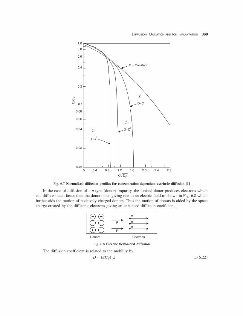
D = DS [C/CS]γ ...(6.17)
where DS = diffusion coefficient at the surface, CS = doping concentration at the surface and γ is apositive integer. In this case the diffusion equation can be solved numerically the results being shownin Fig. 6.7 as a function of normalised distance. γ = 0 corresponds to the case of D = constant. It is foundthat the diffusion profiles are much steeper at low concentrations (C << CS) for concentration-depend-ent diffusion coefficients. The junction depths for values of γ = 1, 2 & 3 are given below:
xj = 1.6 √(DS t) for D ~ C (γ = 1) ...(6.18a)
xj = 1.1 √(DS t) for D ~ C2 (γ = 2) ...(6.18b)
xj = 0.87 √(DS t) for D ~ C3 (γ = 3) ...(6.18c)Thus it is seen that the abruptness of the doping profile gives a junction depth independent of the
background doping concentration.
6.7 FIELD-AIDED DIFFUSION
The presence of a drift field can result in motion of charged impurities in the direction of the electricfield. Assuming that the random scattering of impurities by the lattice gives a resultant drift velocity v,the equation of motion due to an electric field E is given by
F = q Z E = m* dv/dt + α v ...(6.19)
where F = force on impurity ion, qZ = charge of impurity ion, m* = effective mass and α = proportion-ality factor. The direction of the force obviously depends on the sign of the charge on the impurity ion.In the steady state when a steady drift velocity vd is attained
vd = q Z E/α = μ E ...(6.20)
where μ = q Z/α = mobility of impurity ion. If the motion of impurity ions due to drift and diffusionare considered to be independent then the flux density in presence of drift can be written as
( )j D N x NE= − ∂ ∂ + μ ...(6.21)
DIFFUSION, OXIDATION AND ION IMPLANTATION 369
Fig. 6.7 Normalised diffusion profiles for concentration-dependent extrinsic diffusion [1]
In the case of diffusion of a n-type (donor) impurity, the ionised donor produces electrons whichcan diffuse much faster than the donors thus giving rise to an electric field as shown in Fig. 6.8 whichfurther aids the motion of positively charged donors. Thus the motion of donors is aided by the spacecharge created by the diffusing electrons giving an enhanced diffusion coefficient.
Fig. 6.8 Electric field-aided diffusion
The diffusion coefficient is related to the mobility by
D = (kT/q) μ ...(6.22)
1.0
0.8
0.6
0.4
0.2
0.1
0.08
0.06
0.04
0.02
0.010 0.4 0.8 1.2 1.6 2.0 2.4 2.8
C/C
S (a)
(b)
(c)
D~C3
D~C2
D~C
D = Constant
X/ D ts
Donors Electrons
F
F
e�
e�
e�
370 SEMICONDUCTOR MATERIALS & DEVICES
Further in equilibrium the flow of electrons due to drift is balanced by the flow due to diffusion.Thus
( ) ( ) ( )nE D n x kT q n xμ = − ∂ ∂ = μ ∂ ∂ ...(6.23)
Simplifying E kT q n dn dx= −a fa fa f1 ...(6.24)
Substituting in eqn. (6.21)
j = −D (1 + dn/dN) ( )n x∂ ∂ ...(6.25)
Thus the impurities move with an effective diffusion coefficient Deff
Deff = D (1 + dn/dN) ...(6.26)
For an n-type impurity
n/ni = N/2 ni + [(N/2ni)2 + 1]1/2 ...(6.27)
so that dn/dN = 1
2{1 + [1 + (2ni/N)2]−1/2} ...(6.28)
Thus there can be a substantial increase in the effective diffusion coefficient with doping concen-tration, by even a factor of 2. This has been observed experimentally for substitutional diffusers.
Example: Formation of n-p-n transistors by diffusion
It is required to form a p-n junction at a depth of 2 μm below the surface of an n-type Si wafer withn = 1016/cm3. (Given B source concentration N0 = 5 × 10¹⁸/cm3). Find the required diffusion time andtemperature.
For Constant Source diffusion the profile is given by N (x, t) = N0 erfc [x/2 (Dt)1/2] (6.10)
In this problem N (x = 2 μm, t) = 1016 = 5 × 10¹⁸ . erfc [x/2 (Dt)1/2]
∴ erfc [ x/2 (Dt)1/2] = erfc y = 1016/(5 × 1018) = 2 × 10⁻⁴
From erfc tables y = 2.25 = x/2 (Dt)1/2 = (2 × 10⁻⁴)/2 (Dt)1/2
Thus (Dt)1/2 = 4.4 × 10⁻⁵
Let time t = 2 hrs = 7200 s. Then D = 2.5 × 10⁻¹³ cm2/s.
From the B diffusion graphs T = 1080° C.
Thus the required diffusion condition is t = 2 hrs diffusion at T = 1080° C.
Note: This is not an unique answer. If t = 1 hr = 3600 s, T = 1150° C.
Thus, a small change in temperature results in a large change in D due the exponential dependence.Hence the diffusion furnace must be designed to provide ±1° C control in time and along its length.
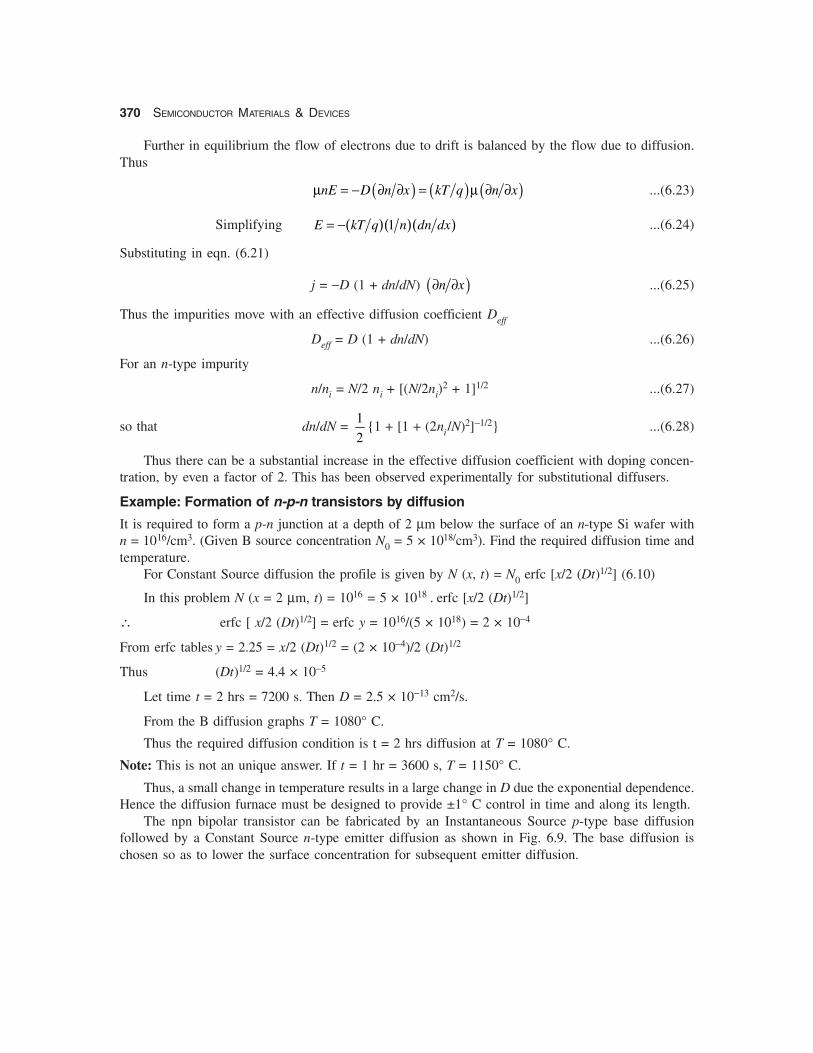
The npn bipolar transistor can be fabricated by an Instantaneous Source p-type base diffusionfollowed by a Constant Source n-type emitter diffusion as shown in Fig. 6.9. The base diffusion ischosen so as to lower the surface concentration for subsequent emitter diffusion.
DIFFUSION, OXIDATION AND ION IMPLANTATION 371
Fig. 6.9 Doping profiles of a n-p-n bipolar transition formed by Instantaneous Source Diffusion (Gaussianprofile) for base followed by Constant Source Diffusion (erfc profile) for emitter [1]
6.8 DIFFUSION SYSTEMS
The choice of dopants in Si and GaAs has been discussed. There are broadly 2 types of diffusionsystems employed (i) open tube and (ii) closed tube. There are some general requirements for diffusionsystems. These are:
(a) the surface concentration should be capable of being controlled over a wide range up to thesolid solubility limit
(b) the diffusion process should not result in any damage to the surface(c) the dopant remaining after diffusion should be capable of easily removed and(d) the system should be reproducible and capable of handling a large number of wafers
simultaneously.
(e) the temperature control should provide a central flat zone with ± 1
2°C variation in temperature.
N
5 × 10²⁰
1019
3 × 10¹⁶
n - type erfc
p - type gaussian
n - type background
0 x
N
N+
P N
0 xAB xBC
EmitterBase Collector
0 1.4 1.7 x( m)�
x
372 SEMICONDUCTOR MATERIALS & DEVICES
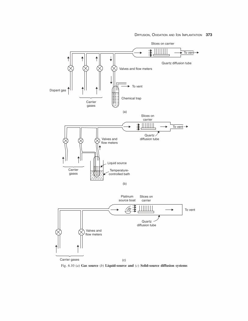
A diffusion furnace is a carefully designed apparatus capable of maintaining uniform temperaturebetween 600 – 1200° C with a feedback controller. The diffusion tube made of high purity fused silicamust be handled with great care, one tube and slice carrier being used for each type of dopant to preventcontamination. The length of the tubes vary from 10 cm – 150 cm or more for industrial furnaces. Forlarge tubes the insertion of the carrier is done mechanically from one end, the other end being used forflow of gases and dopants. The temperature of the furnace is gradually ramped up from 600° C afterinsertion of the wafers with a programmed temperature controller ramping up the temperature at alinear rate of 3 – 10° C/min. This is to prevent thermal shock to the wafers as well as to the tube and components. In practice the diffusion tube is always kept above 600° C and never allowed to cool toroom temperature to avoid devitrification. A gas source diffusion system is shown in Fig. 6.10(a).
If the temperature is ramped down at a rate T = T0 – Ct where T0 = initial temperature andC = constant, it can be shown that this is equivalent to the wafers being subject to an additional timekT0
2/CE0 at the initial diffusion temperature where E0 = activation energy for diffusion.
B Diffusion
The most common p-type impurity is Boron because of its high solid solubility which is 6 × 10²⁰/cm3
as given in Table 6.1. However due to the large misfit factor of B of 0.254 which introduces strain-induced defects, the actual upper limit is 5 × 10¹⁹/cm3. Diffusion systems for Boron in Si are summa-rised in Table 6.5.
Table 6.5 Diffusion Systems for Boron in Si
Impurity R.T state Temp Impurity Advantages Disadvantagessource range (°C) conc. range
BN Solid Pre-oxidise at High & low High surface conc. B skin formation;750 –1100 Sticking to Si
BCl3 Gas R.T High & low Accurate control Halogen pitting
B2H6 Gas R.T High & low Accurate control Highly toxic andexplosive
Solid, liquid and gaseous sources are available for B diffusion. One of the most common is Boricoxide B2O3. A preliminary reaction with B2O3 gives:
2 B2O3 + 3 Si → 4 B + 3 SiO2 ...(6.29)
The Si and B2O3 are kept at the same temperature and pre-deposition is carried out in N2 ambientwith 2–3 % O2. The temperature of the B2O3 controls the surface concentration of B as shown in(Fig. 6.10(c)). Excessive amounts of B2O3 leads to the formation of a B skin which is difficult toremove. Slices are thus exposed to B2O3 source for a short time to form a glassy layer on the Si surface.The source is then removed and drive-in diffusion carried out in an oxidizing ambient. This protects thesurface against impurities. This process gives a 2 step-diffusion profile.
BN slices slightly larger than the Si wafers can be used which can be sandwiched between Si sliceswith a spacing of 2 – 3 mm. These must be pre-oxidised at 750 – 1100° C to form a thin skin of B2O3on the surface which forms the diffusion source:
4 BN + 7 O2 → 2 B2O3 + 4 NO2 ...(6.30)
DIFFUSION, OXIDATION AND ION IMPLANTATION 373
Fig. 6.10 (a) Gas source (b) Liquid-source and (c) Solid-source diffusion systems
Slices on carrier
To vent
Quartz diffusion tube
Valves and flow meters
Dopant gasTo vent
Chemical trapCarriergases
(a)Slices on
carrier
To vent
Quartzdiffusion tubeValves and
flow meters
Liquid source
Carriergases
Temperature-controlled bath
(b)
Platinumsource boat
Slices oncarrier
To vent
Quartzdiffusion tube
Valves andflow meters
Carrier gases (c)
374 SEMICONDUCTOR MATERIALS & DEVICES
No carrier gas is required but a flow of 1 l/min of dry N2 prevents back diffusion of contaminants.This process is extremely reproducible with excellent uniformity across the wafers. To avoid sticking,BN in a silica matrix is often used which also reduces B skin formation.
In thick film technology often used for the fabrication of solar cells, mixtures of B2O3 and SiO2 ina polyvinyl alcohol solvent are used as spin-on sources. Mixtures of carborane and alkylsiloxane whichhave better viscosity control have also been used. An initial bake out is required before diffusion toconvert the components into B2O3 and SiO2.
Gaseous sources Fig. 6.10(a) which are used are diborane (B2H6) and BCl3 which give the follow-ing reactions:
B2H6 + 3 O2 ⎯⎯⎯→300° C B2O3 + 3 H2O ...(6.31)
4 BCl3 + 3 O2 → 2 B2O3 + 6 Cl2 ...(6.32)
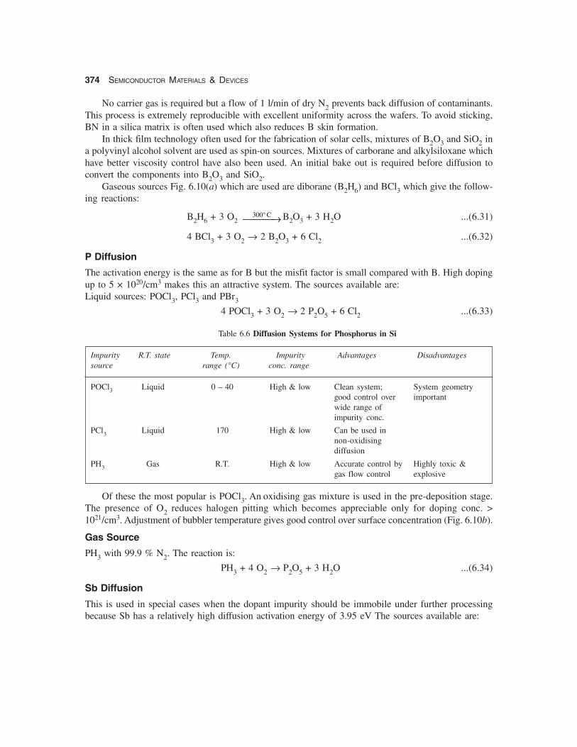
P Diffusion
The activation energy is the same as for B but the misfit factor is small compared with B. High dopingup to 5 × 10²⁰/cm3 makes this an attractive system. The sources available are:Liquid sources: POCl3, PCl3 and PBr3
4 POCl3 + 3 O2 → 2 P2O5 + 6 Cl2 ...(6.33)
Table 6.6 Diffusion Systems for Phosphorus in Si
Impurity R.T. state Temp. Impurity Advantages Disadvantagessource range (°C) conc. range
POCl3 Liquid 0 – 40 High & low Clean system; System geometrygood control over importantwide range ofimpurity conc.
PCl3 Liquid 170 High & low Can be used innon-oxidisingdiffusion
PH3 Gas R.T. High & low Accurate control by Highly toxic &gas flow control explosive
Of these the most popular is POCl3. An oxidising gas mixture is used in the pre-deposition stage.The presence of O2 reduces halogen pitting which becomes appreciable only for doping conc. >1021/cm3. Adjustment of bubbler temperature gives good control over surface concentration (Fig. 6.10b).
Gas Source
PH3 with 99.9 % N2. The reaction is:
PH3 + 4 O2 → P2O5 + 3 H2O ...(6.34)
Sb Diffusion
This is used in special cases when the dopant impurity should be immobile under further processingbecause Sb has a relatively high diffusion activation energy of 3.95 eV The sources available are:
DIFFUSION, OXIDATION AND ION IMPLANTATION 375
Solid sources: Sb2O3 and Sb2O4 at 900° CLiquid sources: Sb3Cl5 in a bubblerIn the last case Sb is transported as an oxide. Diffusion occurs through a glassy layer following
surface reaction with Si.
As Diffusion
As has misfit factor = 0 with Si and hence does not give rise to strain on heavy doping. It is thus usedfor the fabrication of low resistivity epitaxial layers. It is highly toxic and hence the diffusion systemsmust be handled with extreme care. The sources used are:
Solid sources: 2 As2O3 + 3 Si → 3 SiO2 + 4 As ...(6.35)
Gas sources: 2 AsH3 + 3 O2 → As2O3 + 3 H2O ...(6.36)
Au Diffusion
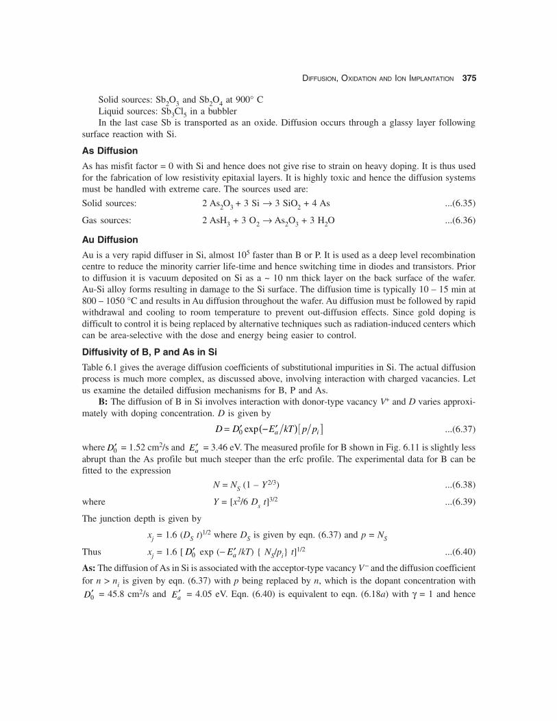
Au is a very rapid diffuser in Si, almost 105 faster than B or P. It is used as a deep level recombinationcentre to reduce the minority carrier life-time and hence switching time in diodes and transistors. Priorto diffusion it is vacuum deposited on Si as a ~ 10 nm thick layer on the back surface of the wafer.Au-Si alloy forms resulting in damage to the Si surface. The diffusion time is typically 10 – 15 min at800 – 1050 °C and results in Au diffusion throughout the wafer. Au diffusion must be followed by rapidwithdrawal and cooling to room temperature to prevent out-diffusion effects. Since gold doping isdifficult to control it is being replaced by alternative techniques such as radiation-induced centers whichcan be area-selective with the dose and energy being easier to control.
Diffusivity of B, P and As in Si
Table 6.1 gives the average diffusion coefficients of substitutional impurities in Si. The actual diffusionprocess is much more complex, as discussed above, involving interaction with charged vacancies. Letus examine the detailed diffusion mechanisms for B, P and As.
B: The diffusion of B in Si involves interaction with donor-type vacancy V+ and D varies approxi-mately with doping concentration. D is given by
D D E kT p pa i= ¢ - ¢0 expa f ...(6.37)
where ¢D0 = 1.52 cm2/s and ¢Ea = 3.46 eV. The measured profile for B shown in Fig. 6.11 is slightly lessabrupt than the As profile but much steeper than the erfc profile. The experimental data for B can befitted to the expression
N = NS (1 – Y2/3) ...(6.38)
where Y = [x2/6 Ds t]3/2 ...(6.39)
The junction depth is given by
xj = 1.6 (DS t)1/2 where DS is given by eqn. (6.37) and p = NS
Thus xj = 1.6 [ ′D0 exp (− ′Ea /kT) { NS/pi} t]1/2 ...(6.40)
As: The diffusion of As in Si is associated with the acceptor-type vacancy V− and the diffusion coefficientfor n > ni is given by eqn. (6.37) with p being replaced by n, which is the dopant concentration with
′D0 = 45.8 cm2/s and ′Ea = 4.05 eV. Eqn. (6.40) is equivalent to eqn. (6.18a) with γ = 1 and hence
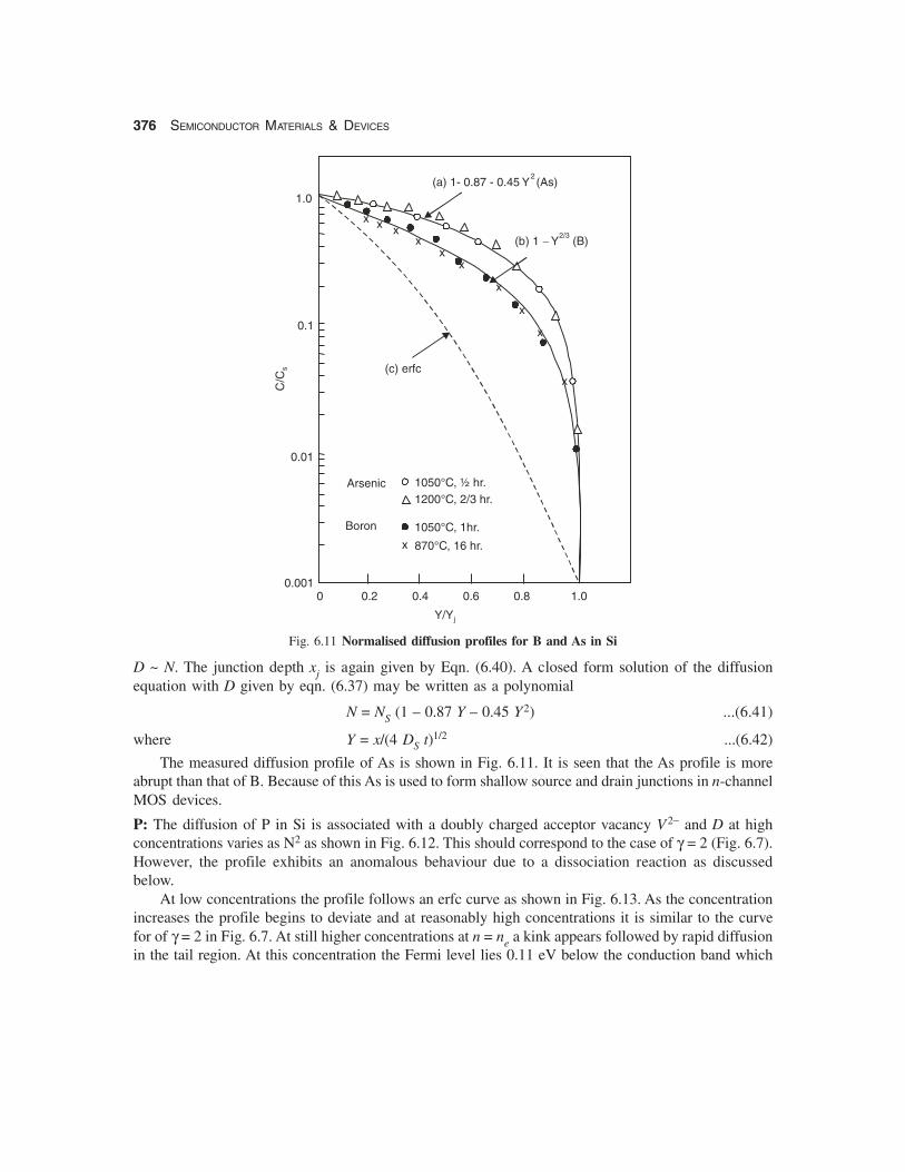
376 SEMICONDUCTOR MATERIALS & DEVICES
Fig. 6.11 Normalised diffusion profiles for B and As in Si
D ~ N. The junction depth xj is again given by Eqn. (6.40). A closed form solution of the diffusionequation with D given by eqn. (6.37) may be written as a polynomial
N = NS (1 – 0.87 Y – 0.45 Y2) ...(6.41)
where Y = x/(4 DS t)1/2 ...(6.42)
The measured diffusion profile of As is shown in Fig. 6.11. It is seen that the As profile is moreabrupt than that of B. Because of this As is used to form shallow source and drain junctions in n-channelMOS devices.
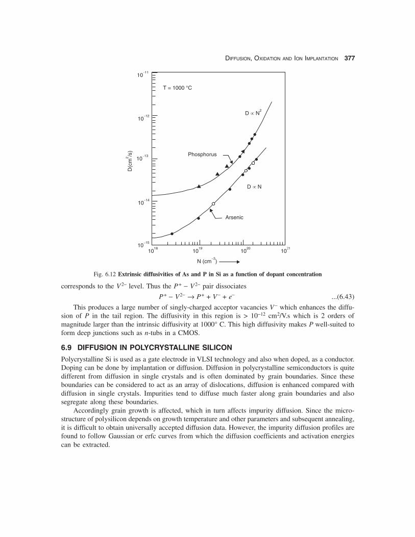
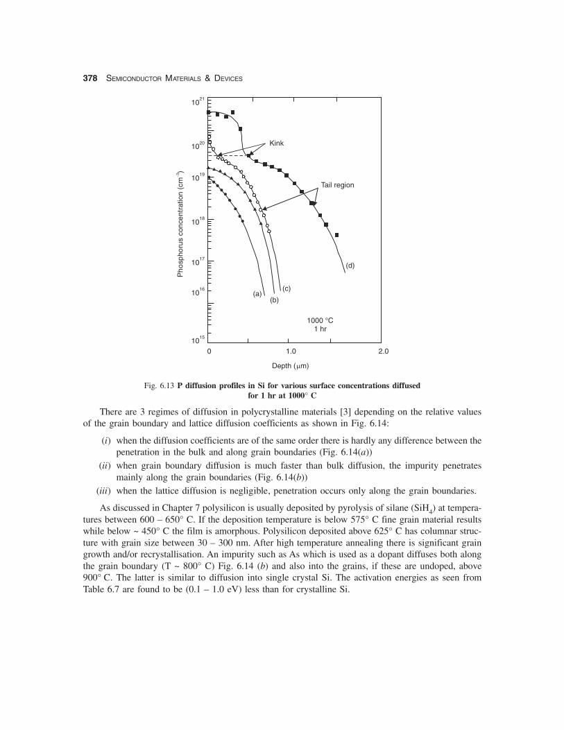
P: The diffusion of P in Si is associated with a doubly charged acceptor vacancy V2− and D at highconcentrations varies as N2 as shown in Fig. 6.12. This should correspond to the case of γ = 2 (Fig. 6.7).However, the profile exhibits an anomalous behaviour due to a dissociation reaction as discussedbelow.
At low concentrations the profile follows an erfc curve as shown in Fig. 6.13. As the concentrationincreases the profile begins to deviate and at reasonably high concentrations it is similar to the curvefor of γ = 2 in Fig. 6.7. At still higher concentrations at n = ne a kink appears followed by rapid diffusionin the tail region. At this concentration the Fermi level lies 0.11 eV below the conduction band which
1.0
0.1
0.01
0.0010 0.2 0.4 0.6 0.8 1.0
(a) 1- 0.87 - 0.45 Y (As)2
(b) 1 Y (B)�2/3
Arsenic 1050°C, ½ hr.1200°C, 2/3 hr.
Boron 1050°C, 1hr.
870°C, 16 hr.
C/C
s
Y/Yj
x
x
x
x
xx
xxxx
x
(c) erfc
DIFFUSION, OXIDATION AND ION IMPLANTATION 377
Fig. 6.12 Extrinsic diffusivities of As and P in Si as a function of dopant concentration
corresponds to the V2− level. Thus the P+ − V2− pair dissociates
P+ − V2− → P+ + V− + e− ...(6.43)
This produces a large number of singly-charged acceptor vacancies V− which enhances the diffu-sion of P in the tail region. The diffusivity in this region is > 10−12 cm2/V.s which is 2 orders ofmagnitude larger than the intrinsic diffusivity at 1000° C. This high diffusivity makes P well-suited toform deep junctions such as n-tubs in a CMOS.
6.9 DIFFUSION IN POLYCRYSTALLINE SILICON
Polycrystalline Si is used as a gate electrode in VLSI technology and also when doped, as a conductor.Doping can be done by implantation or diffusion. Diffusion in polycrystalline semiconductors is quitedifferent from diffusion in single crystals and is often dominated by grain boundaries. Since theseboundaries can be considered to act as an array of dislocations, diffusion is enhanced compared withdiffusion in single crystals. Impurities tend to diffuse much faster along grain boundaries and alsosegregate along these boundaries.
Accordingly grain growth is affected, which in turn affects impurity diffusion. Since the micro-structure of polysilicon depends on growth temperature and other parameters and subsequent annealing,it is difficult to obtain universally accepted diffusion data. However, the impurity diffusion profiles arefound to follow Gaussian or erfc curves from which the diffusion coefficients and activation energiescan be extracted.
10�12
10�13
10�14
10�15
1019
1020
101
N (cm )�3
D(c
m/s
)2
T = 1000 °C
D N2
Phosphorus
Arsenic
D N
1018
378 SEMICONDUCTOR MATERIALS & DEVICES
Fig. 6.13 P diffusion profiles in Si for various surface concentrations diffusedfor 1 hr at 1000° C
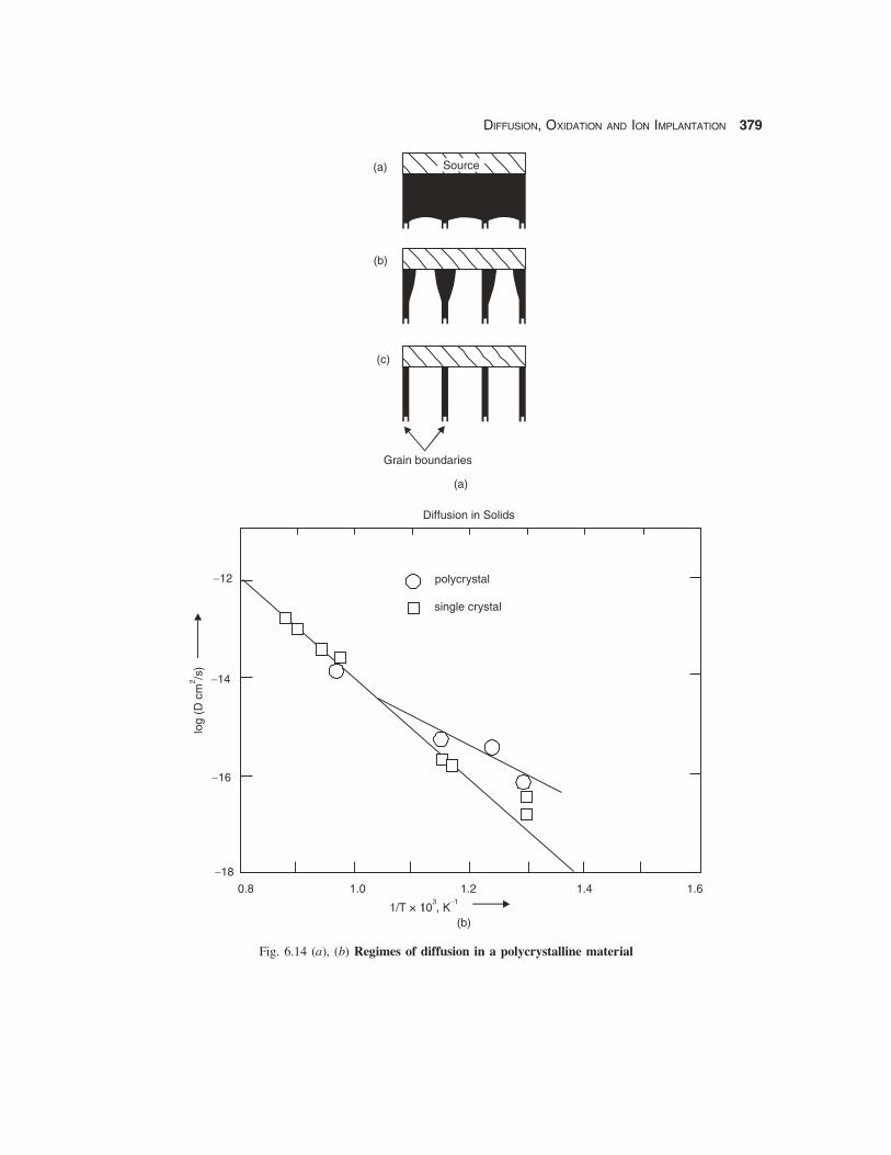
There are 3 regimes of diffusion in polycrystalline materials [3] depending on the relative valuesof the grain boundary and lattice diffusion coefficients as shown in Fig. 6.14:
(i) when the diffusion coefficients are of the same order there is hardly any difference between thepenetration in the bulk and along grain boundaries (Fig. 6.14(a))
(ii) when grain boundary diffusion is much faster than bulk diffusion, the impurity penetratesmainly along the grain boundaries (Fig. 6.14(b))
(iii) when the lattice diffusion is negligible, penetration occurs only along the grain boundaries.
As discussed in Chapter 7 polysilicon is usually deposited by pyrolysis of silane (SiH4) at tempera-tures between 600 – 650° C. If the deposition temperature is below 575° C fine grain material resultswhile below ~ 450° C the film is amorphous. Polysilicon deposited above 625° C has columnar struc-ture with grain size between 30 – 300 nm. After high temperature annealing there is significant graingrowth and/or recrystallisation. An impurity such as As which is used as a dopant diffuses both alongthe grain boundary (T ~ 800° C) Fig. 6.14 (b) and also into the grains, if these are undoped, above900° C. The latter is similar to diffusion into single crystal Si. The activation energies as seen fromTable 6.7 are found to be (0.1 – 1.0 eV) less than for crystalline Si.
1021
1020
1019
1018
1017
1016
1015
0 1.0 2.0
Depth ( m)�
Kink
Tail region
1000 °C1 hr
(a)(b)
(c)
(d)
Pho
spho
rus
conc
entr
atio
n(c
m)
�3
DIFFUSION, OXIDATION AND ION IMPLANTATION 379
Fig. 6.14 (a), (b) Regimes of diffusion in a polycrystalline material
(a)
(b)
(c)
Grain boundaries
Source
(a)
�12
�14
�16
�18
0.8 1.0 1.2 1.4 1.6
Diffusion in Solids
polycrystal
single crystal
log
(Dcm
/s)
2
(b)
380 SEMICONDUCTOR MATERIALS & DEVICES
Table 6.7 Diffusion Data for Polycrystalline Silicon [3]
Element D0 (cm2/s) Ea (eV) D (cm2/s) T (°C)
As 8.6 × 10⁴ 3.9 2.4 × 10⁻¹⁴ 800
0.63 3.2 3.2 × 10⁻¹⁴ 950
B (1.5 – 6) × 10−3 2.4 - 2.5 9 × 10⁻¹⁴ 900
4 × 10⁻¹⁴ 925
P – – 6.9 × 10⁻¹³ 1000
7 × 10⁻¹³ 1000
6.10 ELECTROMIGRATION
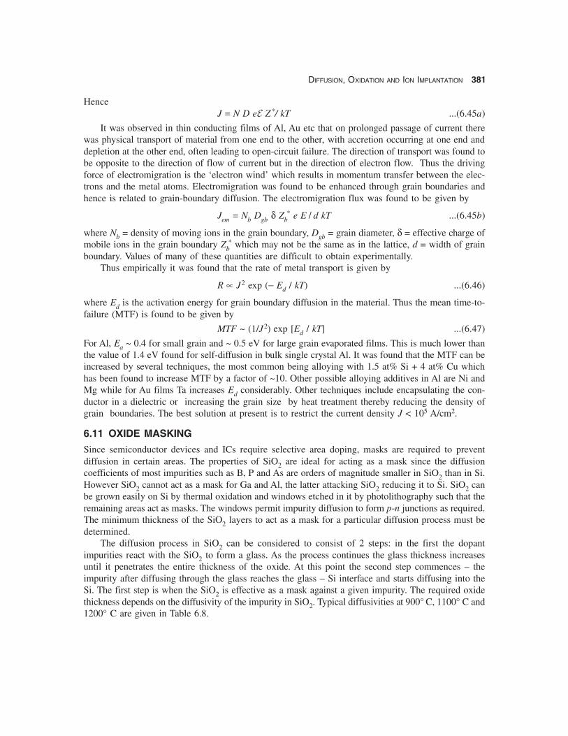
This is the phenomenon of transport of matter due to the flow of an electric current. It is thus differentfrom field-aided diffusion which is the enhancement of diffusion in the direction of an applied electricfield. It was found to be responsible as an important failure mechanism in semiconductor devices andICs operating at high current densities > 104 A/cm2.
When a metal conductor is placed in an electric field E, there are 2 forces acting on metal ions:(i) force F1 due to the electric field E on the metal ions whose magnitude depends on the field and thecharge on the metal ion and is directed in the direction of E towards the negative terminal (ii) force F2due to transfer of momentum from the electron flow to the metal ions and is directed in the oppositedirection towards the positive terminal (Fig. 6.15).
It is the second force that is found to dominate and cause failures. Ideally the simultaneous motionof metal ions cannot cause void formation, but small variations in mobility of the ions along the lengthof the conductor will cause metal ions to move at slightly different rates resulting in the eventualformation of voids.
Fig. 6.15 Electromigration phenomenon
According to the Nernst-Einstein diffusion relation the flux of material is given by
J = NDF/kT ...(6.44a)
where N = density of mobile species, D = their mobility and F = driving force. For the case ofelectromigration
F = eE Z* ...(6.44b)
where E = electric field across conductor and Z * = effective charge on the metal atoms/ions.
E+V �V
F2 F1
ConductorElectron
Metal ion
+
+
DIFFUSION, OXIDATION AND ION IMPLANTATION 381
HenceJ = N D eE Z*/ kT ...(6.45a)
It was observed in thin conducting films of Al, Au etc that on prolonged passage of current therewas physical transport of material from one end to the other, with accretion occurring at one end anddepletion at the other end, often leading to open-circuit failure. The direction of transport was found tobe opposite to the direction of flow of current but in the direction of electron flow. Thus the drivingforce of electromigration is the ‘electron wind’ which results in momentum transfer between the elec-trons and the metal atoms. Electromigration was found to be enhanced through grain boundaries andhence is related to grain-boundary diffusion. The electromigration flux was found to be given by
Jem = Nb Dgb δ Zb* e E /
d kT ...(6.45b)
where Nb = density of moving ions in the grain boundary, Dgb = grain diameter, δ = effective charge ofmobile ions in the grain boundary Zb
* which may not be the same as in the lattice, d = width of grainboundary. Values of many of these quantities are difficult to obtain experimentally.
Thus empirically it was found that the rate of metal transport is given by
R ∝ J2 exp (− Ed / kT) ...(6.46)
where Ed is the activation energy for grain boundary diffusion in the material. Thus the mean time-to-failure (MTF) is found to be given by
MTF ~ (1/J2) exp [Ed / kT] ...(6.47)
For Al, Ea ~ 0.4 for small grain and ~ 0.5 eV for large grain evaporated films. This is much lower thanthe value of 1.4 eV found for self-diffusion in bulk single crystal Al. It was found that the MTF can beincreased by several techniques, the most common being alloying with 1.5 at% Si + 4 at% Cu whichhas been found to increase MTF by a factor of ~10. Other possible alloying additives in Al are Ni andMg while for Au films Ta increases Ed considerably. Other techniques include encapsulating the con-ductor in a dielectric or increasing the grain size by heat treatment thereby reducing the density ofgrain boundaries. The best solution at present is to restrict the current density J < 105 A/cm2.
6.11 OXIDE MASKING
Since semiconductor devices and ICs require selective area doping, masks are required to preventdiffusion in certain areas. The properties of SiO2 are ideal for acting as a mask since the diffusioncoefficients of most impurities such as B, P and As are orders of magnitude smaller in SiO2 than in Si.However SiO2 cannot act as a mask for Ga and Al, the latter attacking SiO2 reducing it to Si. SiO2 canbe grown easily on Si by thermal oxidation and windows etched in it by photolithography such that theremaining areas act as masks. The windows permit impurity diffusion to form p-n junctions as required.The minimum thickness of the SiO2 layers to act as a mask for a particular diffusion process must bedetermined.
The diffusion process in SiO2 can be considered to consist of 2 steps: in the first the dopantimpurities react with the SiO2 to form a glass. As the process continues the glass thickness increasesuntil it penetrates the entire thickness of the oxide. At this point the second step commences – theimpurity after diffusing through the glass reaches the glass – Si interface and starts diffusing into theSi. The first step is when the SiO2 is effective as a mask against a given impurity. The required oxidethickness depends on the diffusivity of the impurity in SiO2. Typical diffusivities at 900° C, 1100° C and1200° C are given in Table 6.8.
382 SEMICONDUCTOR MATERIALS & DEVICES
Table 6.8 Diffusivities of Dopants in SiO2
Element D at 900° C (cm2/s) D at 1100° C (cm2/s) D at 1100° C (cm2/s)
B 3 × 10⁻¹⁹ 3 × 10⁻¹⁷ – 2 × 10⁻¹⁴ 2 × 10⁻¹⁶ - 5 × 10⁻¹⁴
Ga 5 × 10⁻¹¹ 5 × 10⁻⁸
P 1 × 10⁻¹⁸ 2.9 × 10⁻¹⁶ − 2 × 10⁻¹³ 2 × 10⁻¹⁵ – 7.6 × 10⁻¹³
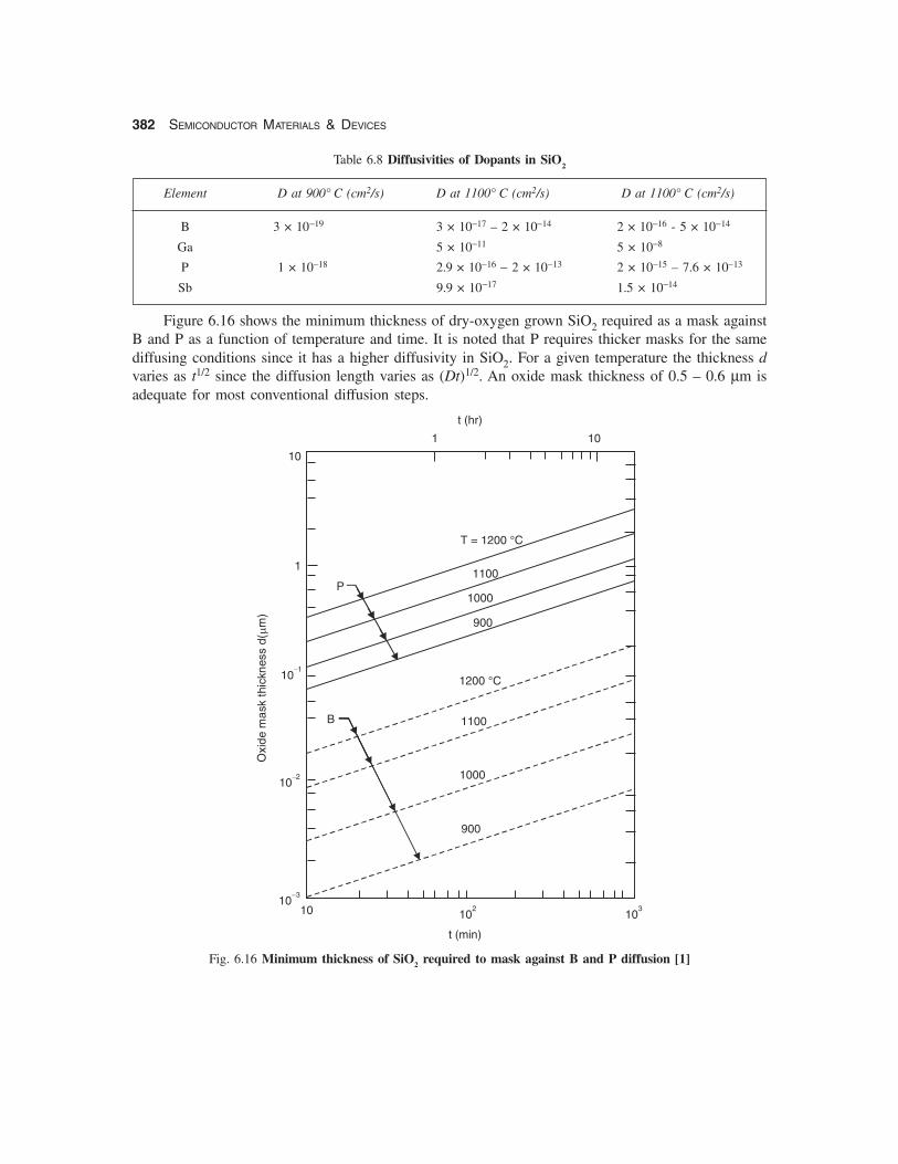
Sb 9.9 × 10⁻¹⁷ 1.5 × 10⁻¹⁴
Figure 6.16 shows the minimum thickness of dry-oxygen grown SiO2 required as a mask againstB and P as a function of temperature and time. It is noted that P requires thicker masks for the samediffusing conditions since it has a higher diffusivity in SiO2. For a given temperature the thickness dvaries as t1/2 since the diffusion length varies as (Dt)1/2. An oxide mask thickness of 0.5 – 0.6 μm isadequate for most conventional diffusion steps.
Fig. 6.16 Minimum thickness of SiO2 required to mask against B and P diffusion [1]
10
1
10�1
10�2
10�3
10 102
103
P
B
t (hr)
t (min)
T = 1200 °C
1100
1000
900
1200 °C
1100
1000
900
Oxi
dem
ask
thic
knes
sd(
m)
�
1 10
DIFFUSION, OXIDATION AND ION IMPLANTATION 383
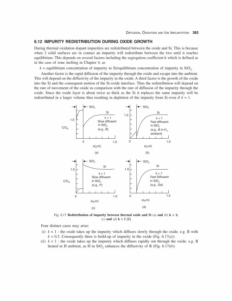
6.12 IMPURITY REDISTRIBUTION DURING OXIDE GROWTH
During thermal oxidation dopant impurities are redistributed between the oxide and Si. This is becausewhen 2 solid surfaces are in contact an impurity will redistribute between the two until it reachesequilibrium. This depends on several factors including the segregation coefficient k which is defined asin the case of zone melting in Chapter 4, as
k = equilibrium concentration of impurity in Si/equilibrium concentration of impurity in SiO2.Another factor is the rapid diffusion of the impurity through the oxide and escape into the ambient.
This will depend on the diffusivity of the impurity in the oxide. A third factor is the growth of the oxideinto the Si and the consequent motion of the Si-oxide interface. Thus the redistribution will depend onthe rate of movement of the oxide in comparison with the rate of diffusion of the impurity through theoxide. Since the oxide layer is about twice as thick as the Si it replaces the same impurity will beredistributed in a larger volume thus resulting in depletion of the impurity from Si even if k = 1.
Fig. 6.17 Redistribution of impurity between thermal oxide and Si (a) and (b) k < 1;(c) and (d) k > 1 [1]
Four distinct cases may arise:
(i) k < 1 : the oxide takes up the impurity which diffuses slowly through the oxide. e.g. B withk = 0.3. Consequently there is build-up of impurity in the oxide (Fig. 6.17(a))
(ii) k < 1 : the oxide takes up the impurity which diffuses rapidly out through the oxide. e.g. Bheated in H ambient, as H in SiO2 enhances the diffusivity of B (Fig. 6.17(b))
1.0
0 1.0
SiO2
Si
k < 1Slow diffusantin SiO2
(e.g., B)
1.0
0 1.0
Si
k < 1Fast diffusantin SiO2
(e.g., B in H2
ambient)
1.0
0 1.0
Si
k > 1Slow diffusantin SiO2
(e.g., P)C/CB
C/CB
1.0
0 1.0
k > 1Fast Diffusantin SiO2
(e.g., Ga)
x( m)�
(d)
(a)
SiO2
SiO2 SiO2
Si
(c)
x( m)�
x( m)� x( m)�
(b)
384 SEMICONDUCTOR MATERIALS & DEVICES
(iii) k > 1 : the oxide rejects the impurity and the diffusivity of the impurity in SiO2 is slow resultingin build-up at the Si interface e.g. k = 10 for P, Sb and As (Fig. 6.17(c))
(iv) k > 1 : the oxide rejects the impurity and the diffusivity of the impurity in SiO2 is rapid so thatthe impurity escapes from the solid into the gaseous ambient that there is overall a depletionof the impurity e.g. Ga with k = 20 and a fast diffuser in SiO2 (Fig. 6.17(d))
In practice redistribution effects are important for B with the surface concentration being reducedto 50% of its value in the absence of redistribution. For P the overall effect is negligible since theredistribution and diffusion effects cancel each other out. The impurities in the oxide are hardly elec-trically active but they affect processing and device properties. The oxidation rate is affected by highdopant concentrations in Si. Non-uniform distribution of impurities in the oxide affect the interface-state properties.
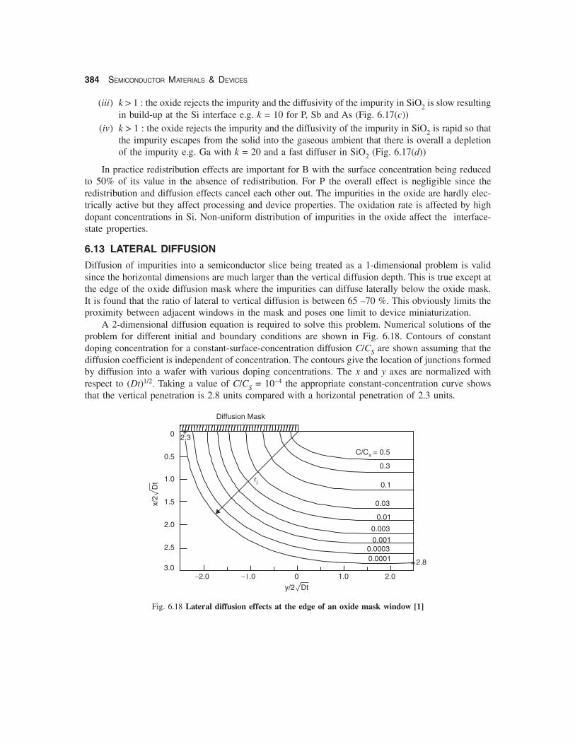
6.13 LATERAL DIFFUSION
Diffusion of impurities into a semiconductor slice being treated as a 1-dimensional problem is validsince the horizontal dimensions are much larger than the vertical diffusion depth. This is true except atthe edge of the oxide diffusion mask where the impurities can diffuse laterally below the oxide mask.It is found that the ratio of lateral to vertical diffusion is between 65 –70 %. This obviously limits theproximity between adjacent windows in the mask and poses one limit to device miniaturization.
A 2-dimensional diffusion equation is required to solve this problem. Numerical solutions of theproblem for different initial and boundary conditions are shown in Fig. 6.18. Contours of constantdoping concentration for a constant-surface-concentration diffusion C/CS are shown assuming that thediffusion coefficient is independent of concentration. The contours give the location of junctions formedby diffusion into a wafer with various doping concentrations. The x and y axes are normalized withrespect to (Dt)1/2. Taking a value of C/CS = 10−4 the appropriate constant-concentration curve showsthat the vertical penetration is 2.8 units compared with a horizontal penetration of 2.3 units.
Fig. 6.18 Lateral diffusion effects at the edge of an oxide mask window [1]
Diffusion Mask
0
0.5
1.0
1.5
2.0
2.5
3.0�2.0 ��.0 0 1.0 2.0
rj
C/C = 0.5s
0.3
0.1
0.03
0.01
0.003
0.0010.00030.0001
x/2
Dt
y/2 Dt
2.8
2.3
DIFFUSION, OXIDATION AND ION IMPLANTATION 385
Lateral diffusion causes p-n junctions to have cylindrical edges with a radius of curvature rj. If themask has sharp corners the shape of the junctions near the corners will be roughly spherical. Cylindricaland spherical junction regions have higher curvature and hence higher avalanche breakdown voltagesthan for planar junctions with the same background doping concentrations.
Gas Immersion Laser Doping (GILD)
A variety of new techniques are being developed for the very shallow junctions (~ 0.05 μm) requiredfor the source and drain regions of state-of-the art MOS devices. Among these are very low energyimplantation, Plasma Immersion Doping and Gas Immersion Laser Doping (GILD). Since implantationmust be followed by anealing at temperatures ~ 1000 °C, this results in impurity redistribution whichincreases junction depth. Plasma immersion doping uses ions from a glow discharge in BF2 for exampleand gives high fluence at low energies. However this suffers from the presence of different types of ionsin a plasma and selectivity is a problem. In the GILD technique a Si wafer is immersed in a precursorgas such as BCl3 which is adsorbed on the surface. High energy uv laser pulses are then incident on thesurface which results in surface melting and impurity diffusion. This technique has been used to achieveB doping upto 4.2 × 10²¹/cm3 (8.4 at %), much above the solid solubility limit of 6 × 10²⁰/cm3.Superconductivity at ambient pressures has been observed for the first time by Bustarret et al. [4] insuch heavily doped Si:B. The transition temperature is however very low 0.35 K with a critical field of0.4 T. The importance lies in the verification of earlier theoretical predictions of superconductivity indiamond-structured materials.
6.14 EVALUATION OF DIFFUSED LAYERS
Three parameters which are important for the evaluation of diffused layers are:
(i) junction depth (ii) sheet resistance and (iii) the doping profile.
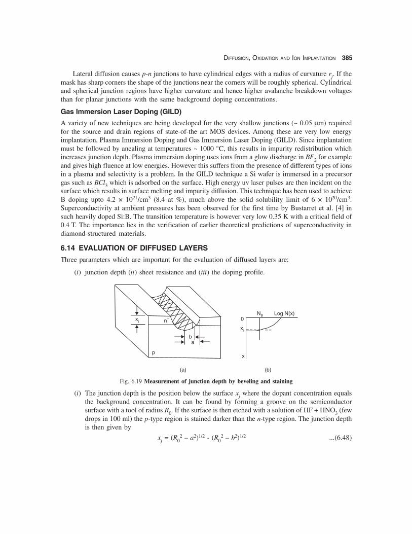
Fig. 6.19 Measurement of junction depth by beveling and staining
(i) The junction depth is the position below the surface xj where the dopant concentration equalsthe background concentration. It can be found by forming a groove on the semiconductorsurface with a tool of radius R0. If the surface is then etched with a solution of HF + HNO3 (fewdrops in 100 ml) the p-type region is stained darker than the n-type region. The junction depthis then given by
xj = (R02 – a2)1/2 - (R0
2 – b2)1/2 ...(6.48)
xj n+
ba
p
(a)
0
xj
NB Log N(x)
(b)
x
386 SEMICONDUCTOR MATERIALS & DEVICES
where a and b are as indicated in Fig. 6.19. If R0 >> a, b, then
xj � (a2 – b2)/2 R0 ...(6.49)
The above technique is subject to errors of geometric measurement and is often supercededby an optical interference technique. This is similar to that described in Chapter 7 for thin filmthickness measurement. The sample surface is lapped at an angle of 12°. An optical flat isplaced on the upper surface of the wafer which is illuminated by collimated monochromaticradiation from a Na vapour lamp at 589.593 and 588.996 nm. The resulting interference fringepattern gives directly the junction depth in terms of the fringe spacing which is ~ 0.29 μm.
Another technique not employed in industry but useful in R & D laboratories where a SEMis available is Electron Beam-Induced Current (EBIC) outlined in Chapter 5. After angle lap-ping as above an electron beam is used to scan the edge of the sample and the beam-inducedcurrent measured. The current goes to zero and changes sign as the beam crosses the junction,the beam diameter being an important factor in the accuracy of the measurement.
(ii) If the junction depth xj and the background doping concentration NB are known the surfaceconcentration NS and the impurity distribution can be calculated provide the doping profilefollows the Constant-Source or Instantaneous Source profiles given by eqns. (6.10) & (6.12).Other techniques of determining the impurity profile are by C-V measurements of a reverse-biased junction which determines the majority carrier or ionized impurity profile (if the impurityatoms are fully ionized). This is discussed in Chapter 8.
A direct technique is using Secondary Ion Mass Spectroscopy (SIMS) discussed in Chapter7. In this atoms are sputtered off by energetic ions and detected in a mass spectrometer. Thusa small crater is formed whose depth can be measure by a stylus. The mass spectrometerdetects the different species and plots the counts vs. time of sputtering. This technique has highsensitivity for B and P and plots the doping profile and finds the junction depth as well. It isideally suited for very shallow junctions and high doping concentrations and has depth resolution~ 10 nm. One difference is that SIMS detects total number of ions present while theC-V and such techniques finds the concentration of ionized impurities. For B & P in Si allimpurities are ionized at 300 K but in the case of impurities with deeper levels this will not bethe case and hence SIMS will give a higher value than that obtained by the C-V technique.(iii) The sheet resistance RS of a diffused layer can be measured using the 4 point probetechnique described in Chapter 1. This is related to the junction depth xj and the carrier mobilityμ (which is a function of the total impurity concentration) and the impurity distribution N(x) by
R q N x dxS
x j
=F
HGG
I
KJJz1
0
/ m a f ...(6.50)
For a given diffusion profile the average resistivity ρ = RS xj is uniquely related to the surfaceconcentration NS and the background concentration NB for an assumed doping profile. Design curvesare available relating the measured ρ with NS for erfc and Gaussian doping profiles. Diagrams plot NSvs. RS . xj with Np as a parameter for the above 2 profiles for n and p-type dopants. Thus measuring RSand xj and knowing NB , the surface concentration NS can be found. This method is accurate for lowconcentrations and deep diffusions provided the profiles follow the assumed types. For high concentrationsand heavy doping the diffusion profiles cannot be represented by the simple functions as discussedearlier.
DIFFUSION, OXIDATION AND ION IMPLANTATION 387
6.15 THERMAL OXIDATION
The Si-SiO2 system together comprise an unique combination which is at the heart of modern ICtechnology and which keeps it ahead of other semiconductor materials with inherently superior prop-erties. In comparison, the thermally grown oxide on GaAs is non-stoichiometric consisting of bothgallium and arsenic oxides and does not have the desirable properties of SiO2. Amorphous SiO2 can begrown or deposited by a number of techniques but it is the thermally grown oxide which has been foundto have the most desirable superior properties. Recently due to its relatively low dielectric constantthere have been attempts to replace SiO2 by other oxides for nanoscale devices with some recentsuccess. These attempts are discussed in Chapter 10. SiO2 has the following important functions inmodern IC technology:
(i) it serves as the gate dielectric i.e. ‘gate oxide’ in MOS devices giving very low interface statedensity and high breakdown field
(ii) it gives surface protection after device fabrication with edges of p-n junctions buried under anoxide layer. It also acts as a ‘field oxide’ in an IC and serves to isolate devices from each other.
(iii) it acts as a diffusion barrier permitting the diffusion of dopants only through windows etchedin it
(iv) it is an excellent dielectric which serves as a substrate on which metal interconnects betweendevices are made and also as an interlayer insulator.
Properties
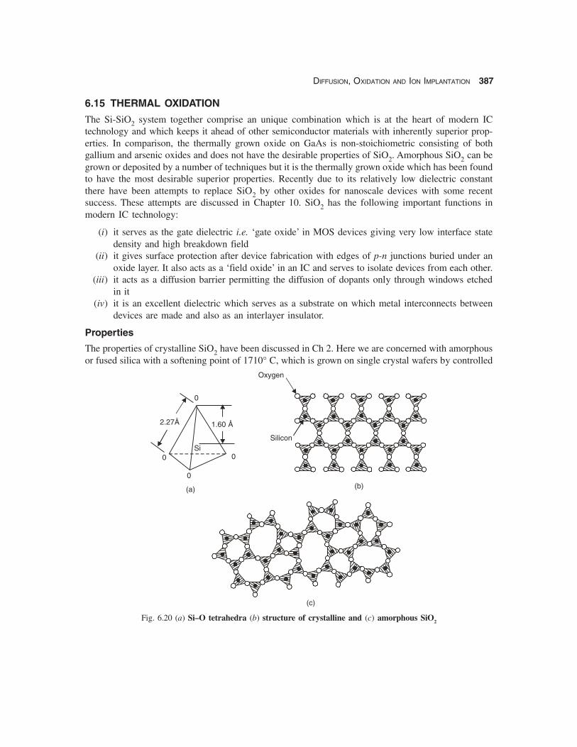
The properties of crystalline SiO2 have been discussed in Ch 2. Here we are concerned with amorphousor fused silica with a softening point of 1710° C, which is grown on single crystal wafers by controlled
Fig. 6.20 (a) Si–O tetrahedra (b) structure of crystalline and (c) amorphous SiO2
0
0
0
2.27Å 1.60 Å
Si
(a) (b)
(c)
Oxygen
Silicon
0
388 SEMICONDUCTOR MATERIALS & DEVICES
heating in dry or wet environments. Structurally it consists of a 3-dimensional random network of Siand O, having coordination numbers of 4 and 2 respectively, forming polyhedra (tetrahedral and trian-gles) with Si4+ at the centre and O2− at the corners (Fig. 6.20). The distance between Si - O ions is 1.62Å while that between O - O is 2.27 Å. These polyhedra are randomly stacked and joined by bridgingand non-bridging oxygen. Crystalline SiO2 contains only bridging oxygen and has a density of 2.65compared with 2.15 – 2.25 for amorphous SiO2. The atomic packing fraction (APF) is only 0.43.
The principal defects in fused silica are O ion vacancies which represent positively charged defects.Fused silica has an open structure which permits interstitial diffusion of impurities. The diffusion of O2.H2O, H2 and Na are represented by Arrhenius plots. The activation energies for O2 and H2O are 1.18eV and 0.79 eV respectively while H and Na have very high diffusivities with low activation energies.Na is important as a contaminant in the thermal oxide. Oxidation involves the transport of a chargedspecies O2
− or O22− through silica to the SiO2 – Si interface where the oxidation takes place.
6.16 OXIDATION SYSTEM
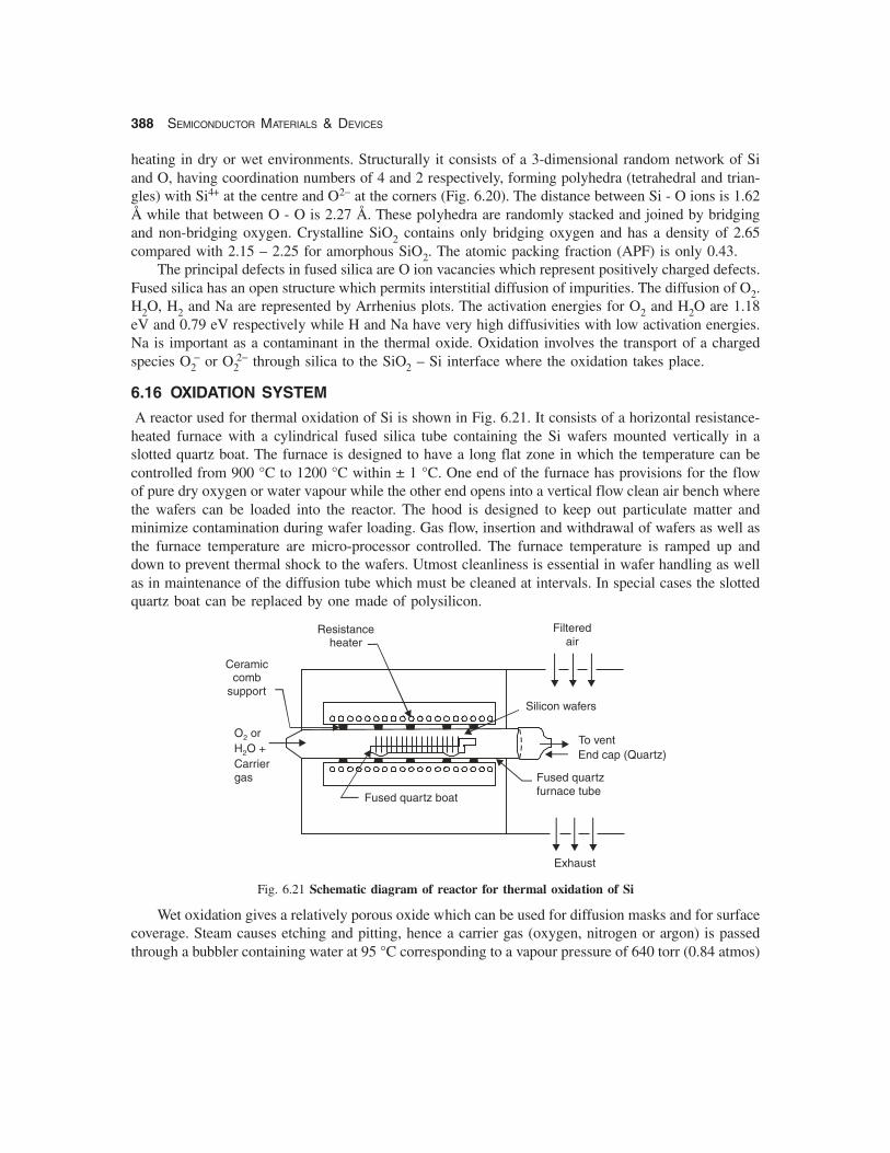
A reactor used for thermal oxidation of Si is shown in Fig. 6.21. It consists of a horizontal resistance-heated furnace with a cylindrical fused silica tube containing the Si wafers mounted vertically in aslotted quartz boat. The furnace is designed to have a long flat zone in which the temperature can becontrolled from 900 °C to 1200 °C within ± 1 °C. One end of the furnace has provisions for the flowof pure dry oxygen or water vapour while the other end opens into a vertical flow clean air bench wherethe wafers can be loaded into the reactor. The hood is designed to keep out particulate matter andminimize contamination during wafer loading. Gas flow, insertion and withdrawal of wafers as well asthe furnace temperature are micro-processor controlled. The furnace temperature is ramped up anddown to prevent thermal shock to the wafers. Utmost cleanliness is essential in wafer handling as wellas in maintenance of the diffusion tube which must be cleaned at intervals. In special cases the slottedquartz boat can be replaced by one made of polysilicon.
Fig. 6.21 Schematic diagram of reactor for thermal oxidation of Si
Wet oxidation gives a relatively porous oxide which can be used for diffusion masks and for surfacecoverage. Steam causes etching and pitting, hence a carrier gas (oxygen, nitrogen or argon) is passedthrough a bubbler containing water at 95 °C corresponding to a vapour pressure of 640 torr (0.84 atmos)
Resistanceheater
Filteredair
Ceramiccomb
support
To ventO orH O +Carriergas
2
2
Fused quartz boat
Silicon wafers
End cap (Quartz)
Fused quartzfurnace tube
Exhaust
DIFFUSION, OXIDATION AND ION IMPLANTATION 389
Kinetics of Oxidation
Thermal oxidation of Si by dry oxygen or water vapour consists of the following reactions:
Si (s) + O2 (g) → SiO2 (s) ...(6.51)
Si (s) + 2 H2O (g) → SiO2 (s) + 2H2 (g) ...(6.52)
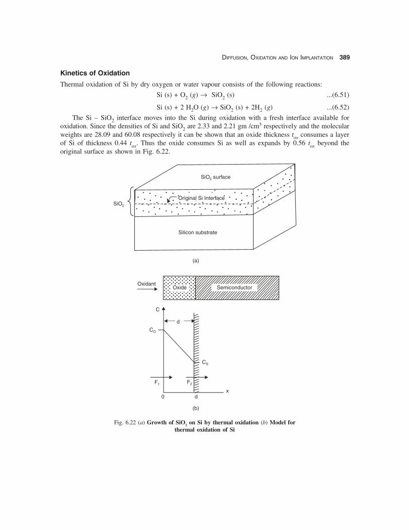
The Si – SiO2 interface moves into the Si during oxidation with a fresh interface available foroxidation. Since the densities of Si and SiO2 are 2.33 and 2.21 gm /cm3 respectively and the molecularweights are 28.09 and 60.08 respectively it can be shown that an oxide thickness tox consumes a layerof Si of thickness 0.44 tox. Thus the oxide consumes Si as well as expands by 0.56 tox beyond theoriginal surface as shown in Fig. 6.22.
Fig. 6.22 (a) Growth of SiO2 on Si by thermal oxidation (b) Model forthermal oxidation of Si
SiO surface2
SiO2
Silicon substrate
Original Si Interface
Oxidant
C
CO
d
0 d
CS
F1 F2
x
Oxide Semiconductor
(a)
(b)
390 SEMICONDUCTOR MATERIALS & DEVICES
The oxidation process consists of
(a) diffusion of O species through the silica(b) reaction of O with Si at the Si – Si O2 interface and(c) rapid out-diffusion of H2 through the silica film.
The growth kinetics can be examined using the model shown in Fig. 6.22(b). Here the oxidantspecies with surface concentration N0 molecules/cm3 is brought into contact with the a-SiO2 surface.The magnitude of N0 is essentially the solid solubility of the species at the oxidation temperaturewhich is:
At 1000° C and 1 atmos. pressure: Dry oxygen – 5.2 × 10¹⁶ molecules/cm3
Water vapour – 3.0 × 10¹⁹ molecules/cm3
Suppose the concentration of the oxidizing species at the Si-SiO2 interface is N1. Transport of thespecies occurs by both drift and diffusion. Drift is ignored in this analysis. If the diffusion coefficientis D, the flux density arriving at the interface is given by Fick’s first law:
J1 = D (∂N/∂x) = D (N0 − N1)/x ...(6.53)
where x = thickness of the grown oxide at a given time.The species then reacts with the Si surface the flux being assumed to be proportional to the
concentration N1 of the species at the surface. Thus
J2 = kN1 ...(6.54)
where k = interfacial reaction rate constant. Under steady-state diffusion conditions these fluxes mustbe equal. Thus combining eqns. (6.53) and (6.54)
J = D N0/(x + D/k) ...(6.55)
Let n = no. of molecules of the oxidizing species that are incorporated into unit volume of theoxide. There are 2.2 × 10²² SiO2 molecules/cm3 in the oxide and for oxidation one molecule of O2 isrequired (eqn. 6.51) compared with 2 molecules of H2O (eqn. 6.52). Thus for oxidation in dry O2n = 2.2 × 10²² molecules/cm3 and for wet oxidation n = 4.4 × 10²² molecules/cm3 Thus the rate ofchange of the oxide layer thickness is given by
dx/dt = j/n = D N0/n (x + D/k) ...(6.56)
Solving this equation with the boundary condition x = 0 at t = 0 gives
x2 + (2 D/k) x = (2 D N0/n) t ...(6.57)
Thus x = (D/k) [(1 + 2 N0 k2 t/D n)1/2 − 1] ...(6.58)
This is a general expression for the oxide thickness as a function of time t.For very small t this reduces to
x = (N0 k/n) t ...(6.59)
and for large values of t
x = (2 D N0/n)1/2 t1/2 ...(6.60)
Thus initially the growth is linear with time and limited by the rate constant k while for longer timesthe growth is parabolic with the diffusion constant D being the limiting factor.
Eqn. (6.57) can be simplified to be written as
x2 + Ax = B t ...(6.61)
DIFFUSION, OXIDATION AND ION IMPLANTATION 391
Eqns (6.59) and (6.60) can then be written
for the linear region as x = (B/A) . t ...(6.62)
and for the parabolic region as x = B1/2 t1/2 ...(6.63)
where the linear rate constant B/A = No k/n. ...(6.64)
and the parabolic rate constant B = 2 D No/n ...(6.65)
A = 2 D/k
An initial oxide layer of thickness d0 may be present. This is easily taken care of in the analysis,eqn. (6.57) being modified to
x2 + (2 D/k) x = (2 D N0/n)(t + τ) ...(6.66)
where τ = (d02 + 2D d0/k) N1/2 D N0 ...(6.67)
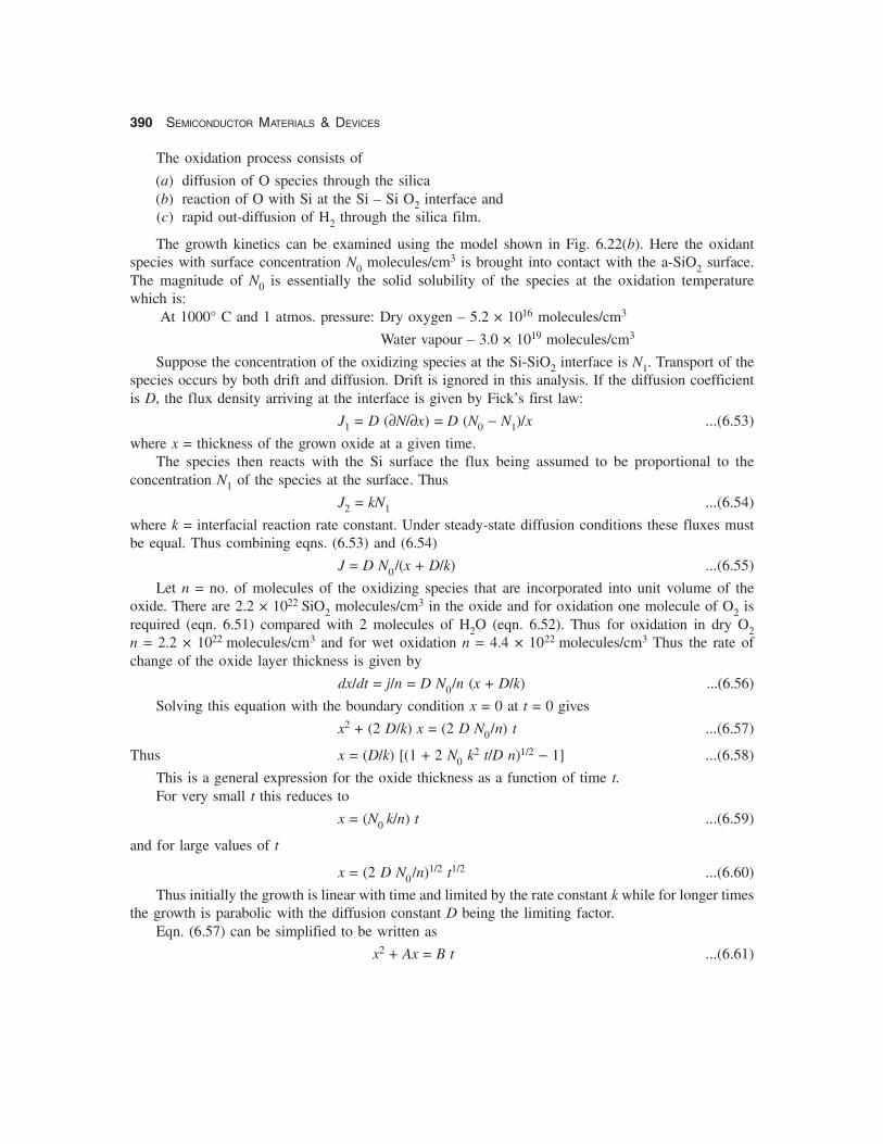
Fig. 6.23 Linear rate constant vs temperature
1200 1100 1000 900 800 700
T(°C)
101
100
10�1
10�
10��
10��
0.6 0.7 0.8 0.9 1.0 1.1
1000/T(K )�1
H O (760 torr)2
E = 2.05 eVa
(111) Si
(100) Si
(111) Si
(100) Si
Dry OE = 2.0 eV
2
d
Line
arra
teco
nsta
ntB
/A(
m/h
r)�
392 SEMICONDUCTOR MATERIALS & DEVICES
which represents the time for the growth of the initial oxide layer. Eqns. (6.59) and (6.60) are thenmodified to
x = (N0 k/n). (t + τ) or x = (B/A) (t + τ) ...(6.68)
and x = (2 D N0/n)1/2 (t + τ)1/2 or x2 = B (t + τ) ...(6.69)
For wet oxidation d0 ≡ 0 but for dry oxidation the extrapolated value of d0 ≡ 20 nm at t = 0.Experimentally determined values of the linear rate constants B/A as a function of temperature are
given in Fig. 6.23 for dry and wet oxidation. The linear rate constant B/A varies as exp (−Ea/ kT) forboth dry and wet oxidation with Ea = ~ 2 eV for both cases. This agrees reasonably well with the energyof 1.83 eV/molecule required to break the Si-Si bond. The growth rate for wet oxidation is largerbecause of a higher value of the rate constant k.The oxidation rate is orientation dependent since thedensity of Si atoms on (111) plane is higher than that on the (100) plane thus providing more sites forincorporation into the SiO2 network.
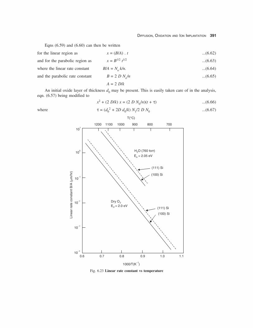
The parabolic rate constant B is plotted in Fig. 6.24 as a function of temperature. The activationenergies for wet and dry oxidation are different as expected since in this region the growth is diffusion-
Fig. 6.24 Parabolic rate constant vs temperature
1200 1100 1000 900 800 700 600 550
100
10��
10�2
10�3
10�4
0.7 0.8 0.9 1.0 1.1 1.2
H O (760 torr)2
E = 0.71 eVa
O (760 torr)2
E = 1.24 eVa
Par
abol
icra
teco
nsta
ntB
(m
/hr)
�2
DIFFUSION, OXIDATION AND ION IMPLANTATION 393
limited. Ea for dry oxidation is 1.24 eV, comparable to the activation energy for diffusion of oxygen infused silica. For wet oxidation Ea = 0.71 eV comparable to the activation energy of water in fused silica.The parabolic rate constant B is independent of orientation because diffusion takes place through arandom network in amorphous silica.
While dry oxidation provides the highest quality oxide for gate dielectrics with high density andlow concentration of traps and interface states, the growth rate is much slower and hence longer timeis required for a thick oxide. Hence, thin gate oxides < 100 nm are grown by dry oxidation while thickfield oxides ~ 500 nm are grown by wet oxidation or a combination of dry-wet-dry steps to providebetter interfacial layers.
Ultra-thin Oxides
In VLSI and ULSI technology with reduced device dimensions the oxide thickness is required to be< 20 nm. It has been seen that an initial oxide layer of this order of thickness exists and hence the abovetheory is not valid for very thin oxide layers. In the early stages of oxide growth large compressivestress exists in the oxide which reduces the diffusion coefficient of O in the oxide. Thus for thin oxidesthe term Ax in eqn. (6.61) can be neglected i.e. D/k is considered very small. Thus this eqn. becomes
x d Bt202− = ...(6.70)
where from eqn. (6.66) d DN N0 0 11 2
2= τb g
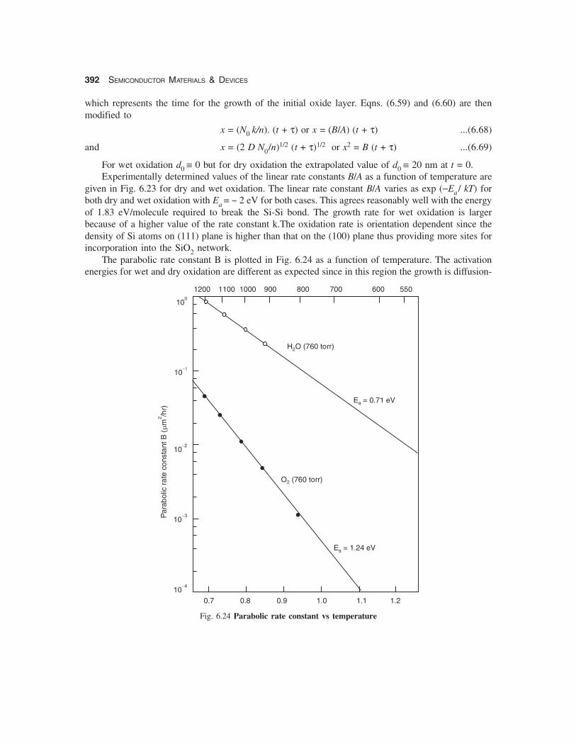
is the initial oxide thickness extrapolated to t = 0. The initial growth in a dry oxide thus follows aparabolic law. Figure 6.25 shows the oxide thickness vs oxidation time for the growth of dry oxide at
Fig. 6.25 Oxide thickness vs. time for thin dry oxides
400
300
200
100
0 20 40 60 80
1030 °C, 0.5 ATM
(a) 1030 °C, 0.1 ATM
980 °C, 0.1 ATM
930 °C, 0.1 ATM
1030 °C, 0.02 ATM
1030 °C, 0.01 ATM
(b)
Oxidation time (min)
Oxi
deth
ickn
ess
(Å)
394 SEMICONDUCTOR MATERIALS & DEVICES
different temperatures and oxygen partial pressures. The solid lines are for the parabolic oxidationequation. It is observed that the initial oxide thickness at t = 0 is d0 = 2.7 nm.
Since B = 2DN0/n and N0 is proportional to the partial pressure P of the oxidizing species in the gasphase, the rate of oxidation depends strongly on the partial pressure as seen from Fig. 6.25.
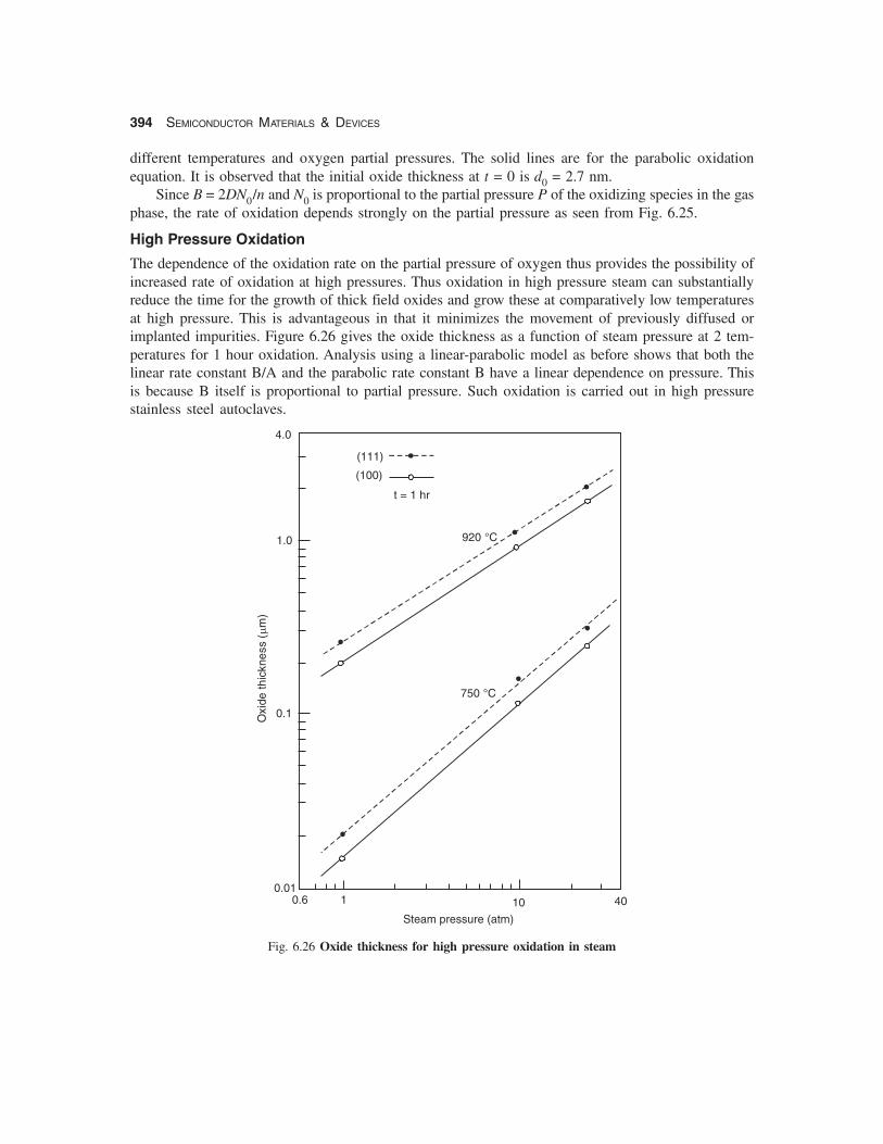
High Pressure Oxidation
The dependence of the oxidation rate on the partial pressure of oxygen thus provides the possibility ofincreased rate of oxidation at high pressures. Thus oxidation in high pressure steam can substantiallyreduce the time for the growth of thick field oxides and grow these at comparatively low temperaturesat high pressure. This is advantageous in that it minimizes the movement of previously diffused orimplanted impurities. Figure 6.26 gives the oxide thickness as a function of steam pressure at 2 tem-peratures for 1 hour oxidation. Analysis using a linear-parabolic model as before shows that both thelinear rate constant B/A and the parabolic rate constant B have a linear dependence on pressure. Thisis because B itself is proportional to partial pressure. Such oxidation is carried out in high pressurestainless steel autoclaves.
Fig. 6.26 Oxide thickness for high pressure oxidation in steam
4.0
1.0
0.1
0.010.6 1 10 40
t = 1 hr
(111)
(100)
920 °C
750 °C
Steam pressure (atm)
Oxi
deth
ickn
ess
(m
)�