diffusion in co fe Õru multilayers - cmu contributed …dl0p/laughlin/pdf/325.pdfdiffusion in...
TRANSCRIPT

JOURNAL OF APPLIED PHYSICS VOLUME 94, NUMBER 2 15 JULY 2003
Diffusion in Co 90Fe10 ÕRu multilayersErik B. Svedberga) and Kent J. HowardSeagate Technology, Pittsburgh, Pennsylvania 15222-4215
Martin C. Bønsager and Bharat B. PantSeagate Technology, Bloomington, Minnesota 55435-5489
Anup G. Roy and David E. LaughlinElectrical and Computer Engineering Department, Carnegie Mellon University, Pittsburgh,Pennsylvania 15213-3890
~Received 13 February 2003; accepted 30 April 2003!
Signal degradation in spin-valve structures is today a concern for long-term stability of data storagedevices. One of the possible degradation mechanisms of spin-valve structures in disk driveapplications could be thermally activated diffusion between constituent layers. In order to predictand control performance degradation, the interdiffusion coefficients for all bilayers in the spin-valvestructure will have to be determined. Here we report results from a Co90Fe10/Ru interface, commonin many spin-valve structures. The diffusion in (0002) oriented polycrystalline Co90Fe10/Rumultilayers has been measured and quantified by x-ray reflectivity in the temperature range of450–540 °C. The bulk diffusion in this case is described by an activation energy ofEa54.95 eV anda prefactor ofD056.4331029 m2/s. No grain boundary diffusion was detected in the large-grainstructure dominated by high symmetry grain boundaries at the temperature interval in this study. Fora spin-valve structure that contains Co90Fe10/Ru interfaces it is clear that with the absence of grainboundary diffusion and a very high activation energy to bulk diffusion degradation will first takeplace at another interface, or by another phenomenon. ©2003 American Institute of Physics.@DOI: 10.1063/1.1586478#
aeni
h-ite
ua
kstsh
wh
ffud
arsayerg.va-av-
the
eed.
in
The
ealerhe-
I. INTRODUCTION
For low diffusivity ~less than 10223m2/s) in thin films,Rutherford backscattering, Auger electron spectroscopy,secondary-ion-mass spectrometry have insufficisensitivity.1 Currently, one of the most sensitive techniquesx-ray diffraction of multilayer structures2,3 where the decayof satellite-peak intensity is related to interdiffusion of neigboring layers. The theory of interdiffusion in artificial compositionally modulated materials is well developed, and insimplest form, the equations are linearized by treating seral parameters as composition independent.4
A multilayer structure can be viewed as periodic modlation of the electron densityc(x), and can be described byFourier series as5
c~x!5 (m52`
1`
Am sinS m2p
LxD . ~1!
In Eq. ~1!, Am is the amplitude of themth order Fouriercomponent,L is the modulation length, andx is the growthdirection. The intensity of the multilayer x-ray satellite peaI m is proportional to the square of the Fourier coefficienI m}Am
2 ; see, for example, Ref. 6. Thus, diffusion, whicleads to a decrease in modulation amplitude, can be vieas a decrease in the intensity of x-ray reflectivity peaks. Tdecrease of satellite intensity is used to calculate the disivity in the continuum approach via the following linearizediffusion equation:4
a!Electronic mail: [email protected]
9930021-8979/2003/94(2)/993/8/$20.00
Downloaded 21 Nov 2003 to 128.2.132.41. Redistribution subject to AI
ndt
s
-
sv-
-
:
ede-
d
dt~ ln I m!522DS 2pm
L D 2
, ~2!
whereD is the effective interdiffusion coefficient. This isstandard method for studying interdiffusion in multilayeand superlattices, and is valid except when the repeated lthicknessL is of the same order as the interatomic spacin4
From the temperature dependence of the diffusivity, actition energyEa can be extracted assuming Arrhenius behior,
D5D0 expS 2Ea
kTD⇔ ln D5 ln D02Ea
kT. ~3!
Equation ~3! describes the temperature dependence ofdiffusivity where k is the Boltzmann constant andT is theabsolute temperature. Thus, by plotting the logarithm ofD asa function of 1/T the activation energy is given by the slopof the graph. For a more detailed description of the linearizdiffusion equation, the reader is referred to Refs. 4 and 7
II. EXPERIMENT
Multilayers of Co90Fe10/Ru were deposited on 3 in. Swafers with a 100 nm SiO2 layer by magnetron sputtering i4 – 5 mTorr Ar gas. The Co90Fe10 layer thickness was;2 nm and the Ru thickness;1 nm. The 3 nm bilayer wasrepeated 15 times and capped with an 8 nm TaN cap.seed layer was 5 nm (Ni80Fe20)60Cr40. The multilayer struc-tures were subsequently annealed in a rapid thermal ann~RTA! in which Ar gas was used to continuously purge tquartz chamber. The O2 levels were monitored during an
© 2003 American Institute of Physics
P license or copyright, see http://ojps.aip.org/japo/japcr.jsp
rtaerng
tiinee
asec
tnd
ic
r,Feside
km
ed
2
the
er.)terible
ta
e.lla-s,ted
eakre-eachal-yas
s
lly
abedf
th
ak
pl
.thak
994 J. Appl. Phys., Vol. 94, No. 2, 15 July 2003 Svedberg et al.
nealing and kept below 2.0 ppm. The RTA employs qualamps for heating and the temperature is controlled by a cbrated pyrometer. The multilayers were heated at temptures ranging from 450 to 540 °C for periods of time rangifrom 300 to 6.43104 s.
The annealed samples were analyzed by x-ray reflecity to determine the degree of interdiffusion, describedSec. I. The measurements were done with a Philips X’Psystem equipped with a Cu anode. Each sample was msured by x-ray reflectivity prior to annealing in the RTAwell as after. In addition, high-resolution transmission eltron microscopy cross sections were used to determinemicrostructure of the samples. A JEOL JEM 2000-EXII aa Philips TECNAI F20 were used for this.
III. RESULTS
A. X-ray diffraction
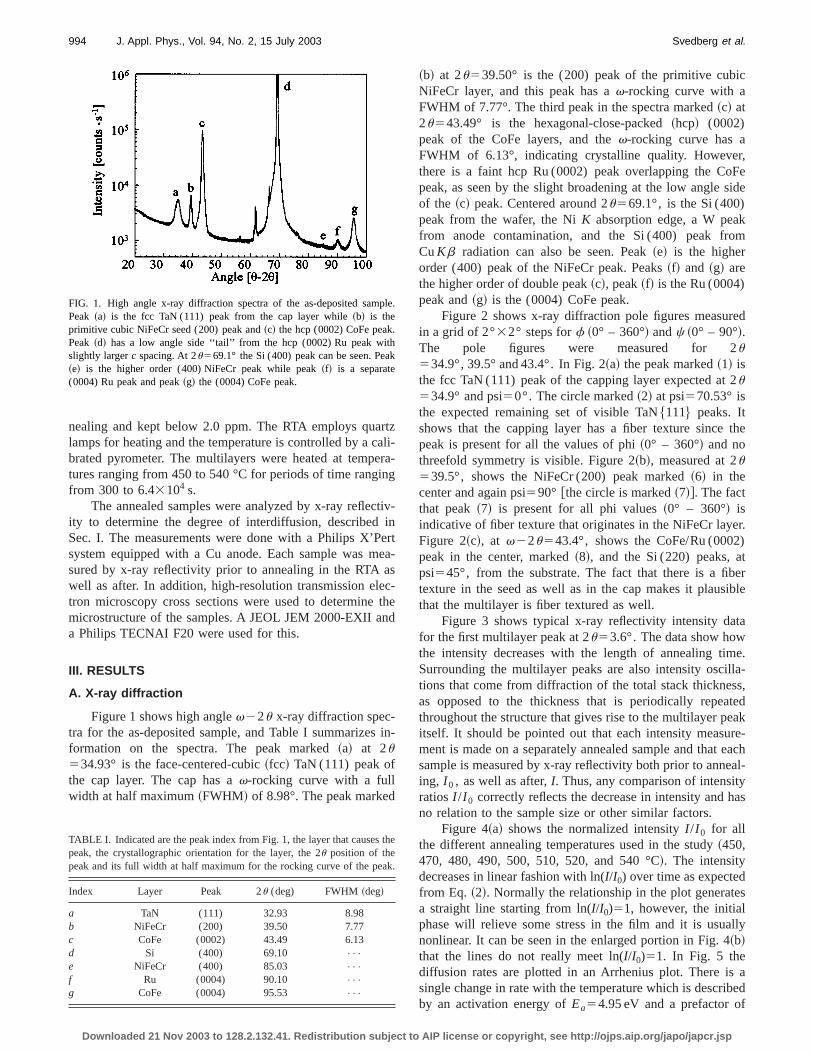
Figure 1 shows high anglev22u x-ray diffraction spec-tra for the as-deposited sample, and Table I summarizesformation on the spectra. The peak marked~a! at 2u534.93° is the face-centered-cubic~fcc! TaN (111) peak ofthe cap layer. The cap has av-rocking curve with a fullwidth at half maximum~FWHM! of 8.98°. The peak marked
TABLE I. Indicated are the peak index from Fig. 1, the layer that causespeak, the crystallographic orientation for the layer, the 2u position of thepeak and its full width at half maximum for the rocking curve of the pe
Index Layer Peak 2u (deg) FWHM ~deg!
a TaN (111) 32.93 8.98b NiFeCr (200) 39.50 7.77c CoFe (0002) 43.49 6.13d Si (400) 69.10 •••
e NiFeCr (400) 85.03 •••
f Ru (0004) 90.10 •••
g CoFe (0004) 95.53 •••
FIG. 1. High angle x-ray diffraction spectra of the as-deposited samPeak ~a! is the fcc TaN (111) peak from the cap layer while~b! is theprimitive cubic NiFeCr seed (200) peak and~c! the hcp (0002) CoFe peakPeak ~d! has a low angle side ‘‘tail’’ from the hcp (0002) Ru peak wislightly largerc spacing. At 2u569.1° the Si (400) peak can be seen. Pe~e! is the higher order (400) NiFeCr peak while peak~f! is a separate(0004) Ru peak and peak~g! the (0004) CoFe peak.
Downloaded 21 Nov 2003 to 128.2.132.41. Redistribution subject to AI
zli-a-
v-
rta-
-he
in-
~b! at 2u539.50° is the (200) peak of the primitive cubNiFeCr layer, and this peak has av-rocking curve with aFWHM of 7.77°. The third peak in the spectra marked~c! at2u543.49° is the hexagonal-close-packed~hcp! (0002)peak of the CoFe layers, and thev-rocking curve has aFWHM of 6.13°, indicating crystalline quality. Howevethere is a faint hcp Ru (0002) peak overlapping the Copeak, as seen by the slight broadening at the low angleof the ~c! peak. Centered around 2u569.1°, is the Si (400)peak from the wafer, the NiK absorption edge, a W peafrom anode contamination, and the Si (400) peak froCuKb radiation can also be seen. Peak~e! is the higherorder (400) peak of the NiFeCr peak. Peaks~f! and ~g! arethe higher order of double peak~c!, peak~f! is the Ru (0004)peak and~g! is the (0004) CoFe peak.
Figure 2 shows x-ray diffraction pole figures measurin a grid of 2°32° steps forf ~0° – 360°! andc ~0° – 90°!.The pole figures were measured for 2u534.9°, 39.5° and 43.4°. In Fig. 2~a! the peak marked~1! isthe fcc TaN (111) peak of the capping layer expected atu534.9° and psi50°. The circle marked~2! at psi570.53° isthe expected remaining set of visible TaN$111% peaks. Itshows that the capping layer has a fiber texture sincepeak is present for all the values of phi~0° – 360°! and nothreefold symmetry is visible. Figure 2~b!, measured at 2u539.5°, shows the NiFeCr (200) peak marked~6! in thecenter and again psi590° @the circle is marked~7!#. The factthat peak~7! is present for all phi values~0° – 360°! isindicative of fiber texture that originates in the NiFeCr layFigure 2~c!, at v22u543.4°, shows the CoFe/Ru (0002peak in the center, marked~8!, and the Si (220) peaks, apsi545°, from the substrate. The fact that there is a fibtexture in the seed as well as in the cap makes it plausthat the multilayer is fiber textured as well.
Figure 3 shows typical x-ray reflectivity intensity dafor the first multilayer peak at 2u53.6°. The data show howthe intensity decreases with the length of annealing timSurrounding the multilayer peaks are also intensity oscitions that come from diffraction of the total stack thicknesas opposed to the thickness that is periodically repeathroughout the structure that gives rise to the multilayer pitself. It should be pointed out that each intensity measument is made on a separately annealed sample and thatsample is measured by x-ray reflectivity both prior to anneing, I 0 , as well as after,I. Thus, any comparison of intensitratiosI /I 0 correctly reflects the decrease in intensity and hno relation to the sample size or other similar factors.
Figure 4~a! shows the normalized intensityI /I 0 for allthe different annealing temperatures used in the study~450,470, 480, 490, 500, 510, 520, and 540 °C!. The intensitydecreases in linear fashion with ln(I/I0) over time as expectedfrom Eq. ~2!. Normally the relationship in the plot generatea straight line starting from ln(I/I0)51, however, the initialphase will relieve some stress in the film and it is usuanonlinear. It can be seen in the enlarged portion in Fig. 4~b!that the lines do not really meet ln(I/I0)51. In Fig. 5 thediffusion rates are plotted in an Arrhenius plot. There issingle change in rate with the temperature which is describy an activation energy ofEa54.95 eV and a prefactor o
e
.
e.
P license or copyright, see http://ojps.aip.org/japo/japcr.jsp

ctyon
mre
20ig.rlyyer,
i-).t
he160,
dl-540
her
995J. Appl. Phys., Vol. 94, No. 2, 15 July 2003 Svedberg et al.
D056.4331029 m2/s. As is seen, the data are a linear funtion of ln(D) in the whole temperature interval. The lineariof the whole region implies that there is only one activatienergy, that of bulk diffusion or grain boundary diffusion.
Figure 6 shows cross sectional transmission electroncroscopy~TEM! images of the multilayered sample structu
FIG. 2. X-ray diffraction pole figures for 2u5 ~a! 34.9°, ~b! 39.5° and~c!43.4°. In ~a! the peak marked~1! is the fcc TaN (111) peak. The circlemarked~2! at 70.5° is the TaN$111% plane set expected at 70.5°. The addtional peaks marked~3!, ~4!, and ~5! are the Si (111), (220), and (113peaks, respectively, from the single crystalline (l00) oriented Si substrate~b! Primitive cubic NiFeCr (200) peak marked~6! in the center and again apsi590°, marked~7!. ~c! CoFe/Ru (0002) peak in the center, marked~8!,and the Si (220) peaks, at psi545°, from the substrate.
Downloaded 21 Nov 2003 to 128.2.132.41. Redistribution subject to AI
-
i-
for the as-deposited film, a film annealed at 500 °C formin and a film annealed at 540 °C for 20 min. In both F6~a! and 6~b! the CoFe/Ru multilayer structure can be cleaseen together with the TaN cap and the NiFeCr seed la
FIG. 3. X-ray reflectivity intensity data for the first multilayer peak at 2u53.6°. The intensity,I, is seen to decrease with the annealing time. Ttemperature of the anneal was 540 °C. Intensity data are shown for 80,240, and 300 s as well as for the as-deposited intensity.
FIG. 4. ~a! X-ray diffraction intensity data for different annealing times antemperatures. The intensity,I, is normalized to the intensity prior to anneaing, I 0 . The temperatures were 450, 470, 480, 490, 500, 510, 520, and°C. The annealing times varied from 300 to 6.43104 s. ~b! Enlargement ofthe time from 0 to 6000 s that show the data for the shorter times/higtemperatures more clearly.
P license or copyright, see http://ojps.aip.org/japo/japcr.jsp

aeed ace
agestheringn.
-
-
ntThe
sof
aretheow
itedset
hea is
edse-
.
e-f
of-
996 J. Appl. Phys., Vol. 94, No. 2, 15 July 2003 Svedberg et al.
even though diffusion has reduced the intensity ratioI /I 0 inFig. 6~b! to ;0.87. In Fig. 6~c!, on the other hand, theCoFe/Ru multilayer structure as well as the seed layerlost; only the TaN cap is unaffected by annealing. Figurshows 1.030.5mm2 atomic force microscopy images of thTaN surface of the, as-deposited film and that anneale
FIG. 5. Diffusion data for the Co90Fe10 /Ru system in an Arrhenius plot. Thdiffusion rates are plotted vs 1/T. There is one diffusion rate which is described by an activation energy ofEa54.9560.25 eV and a prefactor oD056.4331029 m2/s.
FIG. 6. TEM images of the sample structure for~a! the as-deposited film,~b! a film annealed at 500 °C for 20 min and~c! a film annealed at 540 °Cfor 20 min.
Downloaded 21 Nov 2003 to 128.2.132.41. Redistribution subject to AI
re7
at540 °C for 20 min; the two images have the same surffeature size and surface roughness. The fact that the imare identical shows that the cap layer is unaffected byannealing process and as such protects the multilayer duthe annealing process without ‘‘participating’’ in the reactio
B. Transmission electron diffraction
Electron diffraction patterns from plan view TEM images are shown in Figs. 8~a!–8~c!. The diffraction patternswere taken from areas approximately 500 nm3500 nm in allthree images. Figure 8~a! shows an electron diffraction pattern from a single crystallographic domain, while Fig. 8~b!shows an electron diffraction pattern from a slightly differearea that displays two patterns rotated 60° to each other.enlarged electron diffraction pattern area in Fig. 8~c! fromthe single domain pattern in Fig. 8~a! is indexed and showsthe TaN (111), Ru (1010̄) and the CoFe (1010̄) spots aswell as the Ru (1120̄) and the CoFe (1120̄) and higher ordersof Ru (1010̄) and CoFe (1010̄) spots. The diffraction patternare consistent with x-ray diffraction data regarding the outplane orientation of the layers. However, the TEM dataderived from a smaller sample area and as such not showfiber texture in the plane as the x-ray data, but instead shonly one or a few crystallographic domains.
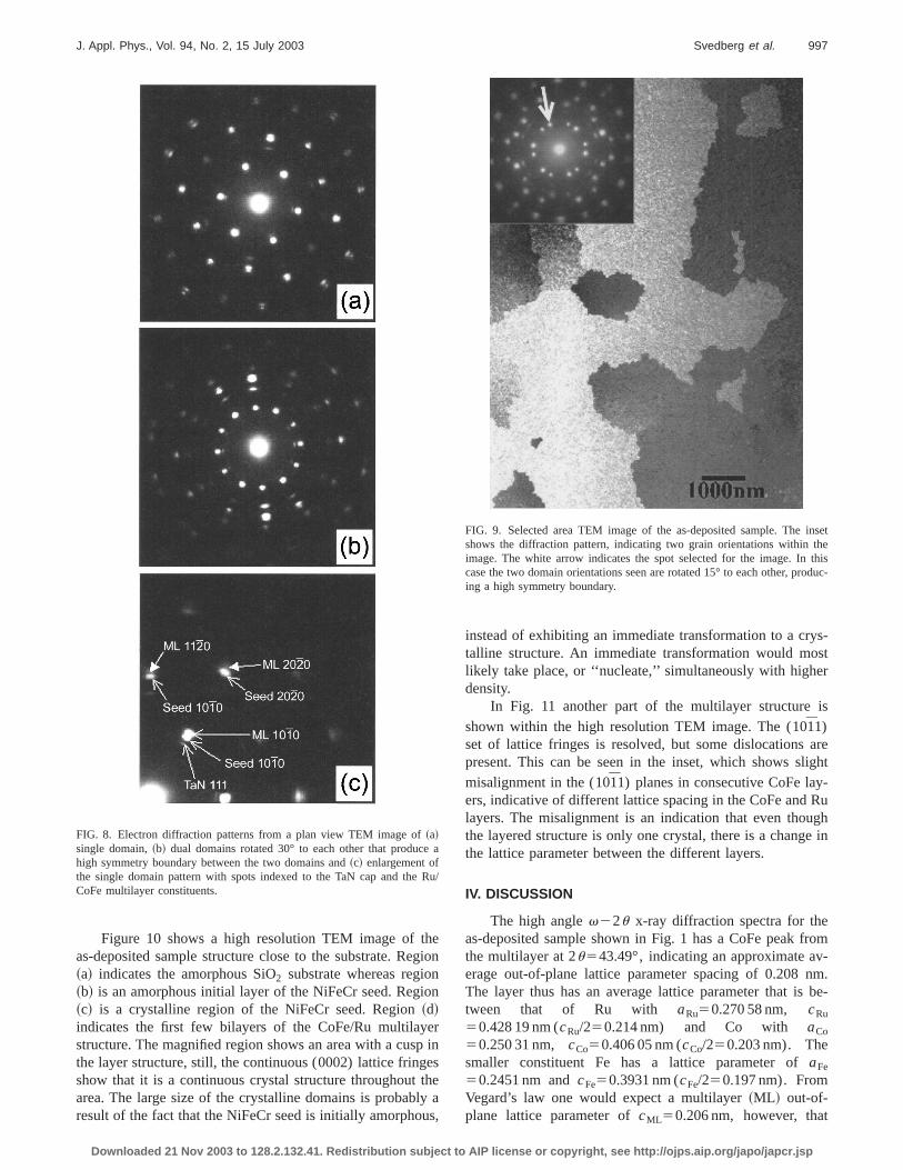
A selected area TEM was produced for an as-depossample. In Fig. 9 the diffraction pattern is shown in the inwith an arrow marking the selected double (1010̄) diffractionspot. The TEM plan view in Fig. 9 shows the size of tgrains in the structure. The estimated grain boundary are9.03104 nm2 for eachmm3 of multilayer film. The grainsare very large in comparison to what is normally observfor thin films deposited at room temperature and as a conquence the samples have very little grain boundary area
FIG. 7. 130.5mm2 atomic force microscopy images of the TaN surfacethe ~a! as-deposited film and~b! the film annealed until the multilayer structure is completely interdiffused.
P license or copyright, see http://ojps.aip.org/japo/japcr.jsp
hegnio
epethlyus
ys-str
is
areight-
Rughe in
rom-
nm.be-
t
e
R
insethethisoduc-
997J. Appl. Phys., Vol. 94, No. 2, 15 July 2003 Svedberg et al.
Figure 10 shows a high resolution TEM image of tas-deposited sample structure close to the substrate. Re~a! indicates the amorphous SiO2 substrate whereas regio~b! is an amorphous initial layer of the NiFeCr seed. Reg~c! is a crystalline region of the NiFeCr seed. Region~d!indicates the first few bilayers of the CoFe/Ru multilaystructure. The magnified region shows an area with a custhe layer structure, still, the continuous (0002) lattice fringshow that it is a continuous crystal structure throughoutarea. The large size of the crystalline domains is probabresult of the fact that the NiFeCr seed is initially amorpho
FIG. 8. Electron diffraction patterns from a plan view TEM image of~a!single domain,~b! dual domains rotated 30° to each other that produchigh symmetry boundary between the two domains and~c! enlargement ofthe single domain pattern with spots indexed to the TaN cap and theCoFe multilayer constituents.
Downloaded 21 Nov 2003 to 128.2.132.41. Redistribution subject to AI
ion
n
rinsea,
instead of exhibiting an immediate transformation to a crtalline structure. An immediate transformation would molikely take place, or ‘‘nucleate,’’ simultaneously with highedensity.
In Fig. 11 another part of the multilayer structureshown within the high resolution TEM image. The (1011̄)set of lattice fringes is resolved, but some dislocationspresent. This can be seen in the inset, which shows slmisalignment in the (1011̄) planes in consecutive CoFe layers, indicative of different lattice spacing in the CoFe andlayers. The misalignment is an indication that even thouthe layered structure is only one crystal, there is a changthe lattice parameter between the different layers.
IV. DISCUSSION
The high anglev22u x-ray diffraction spectra for theas-deposited sample shown in Fig. 1 has a CoFe peak fthe multilayer at 2u543.49°, indicating an approximate average out-of-plane lattice parameter spacing of 0.208The layer thus has an average lattice parameter that istween that of Ru with aRu50.270 58 nm, cRu
50.428 19 nm (cRu/250.214 nm) and Co with aCo
50.250 31 nm, cCo50.406 05 nm (cCo/250.203 nm). Thesmaller constituent Fe has a lattice parameter ofaFe
50.2451 nm andcFe50.3931 nm (cFe/250.197 nm). FromVegard’s law one would expect a multilayer~ML ! out-of-plane lattice parameter ofcML50.206 nm, however, tha
a
u/
FIG. 9. Selected area TEM image of the as-deposited sample. Theshows the diffraction pattern, indicating two grain orientations within timage. The white arrow indicates the spot selected for the image. Incase the two domain orientations seen are rotated 15° to each other, pring a high symmetry boundary.
P license or copyright, see http://ojps.aip.org/japo/japcr.jsp

esnthagBepin
ks
s4
th
g2
atvephatofin
ion,h-
raller
tity
raytal-
uthth
he
on
998 J. Appl. Phys., Vol. 94, No. 2, 15 July 2003 Svedberg et al.
does not take into consideration the differences in stiffnamong Ru, Co and Fe, which makes the value of 0.208plausible. The separation of the higher order peaks formultilayer constituents indicates that the use of an avermultilayer lattice parameter is not completely accurate.using the Ru and CoFe (0004) peaks that are clearly srated at 2u590.15° and 95.65° the lattice (0004) spacingthe Ru layers is given bydRu (0004)51.0879 nm and for CoFeby dCoFe (0004)51.0394 nm. The position of the (0004) peaindicates a shift~enlargement! of thec-axis parameter for Ruto DcRu50.0068 nm and for CoFe toDcCoFe50.0304 nmcompared to bulk values. Since both increase insteadshifting towards an average value there is probably stresthe film. The accuracy in the determination of the Si (00peak and hence the diffractometer measurement isDcSi
50.0012 nm, almost an order of magnitude smaller thanshifts. The fact that the CoFec axis is ;96% of the Ruc
axis can also be seen as a shift in the (1011̄) lattice fringes,for consecutive CoFe layers, in the inset of the TEM imain Fig. 11. The TaN (111) peak from the cap layer atu
FIG. 10. High resolution TEM image of the sample structure. Region~a!indicates the amorphous SiO substrate whereas region~b! is an initial amor-phous region of the NiFeCr seed. Region~c! is a crystalline region of theNiFeCr seed. Region~d! indicates the first few bilayers of the CoFe/Rmultilayer structure. The magnified region shows an area with a cusp inlayer structure and that it is a continuous crystal structure throughoutarea.
Downloaded 21 Nov 2003 to 128.2.132.41. Redistribution subject to AI
smee
ya-
ofin)
e
e
534.93° and the (0002) peak of NiFeCr at 2u539.50° areboth at the positions expected in the x-ray spectra.
The x-ray diffraction pole figures in Fig. 2 measured2u values of 2u534.9°, 39.5° and 43.4° are representatiof fcc TaN (111), primitive cubic NiFeCr (200), and hcCoFe (0002), respectively. It is possible to conclude tthere is a fiber texture in the multilayer from two piecesdata. First, the pole figures in Fig. 2 indicate a fiber texturethe top most TaN layer. Second, the TEM electron diffractpattern in Fig. 8~c! indicates perfect registry, within a grainof the crystal orientation of the bottom NiFeCr seed througout the multilayer up to the TaN cap. Thus, when the ovefilm shows a fiber texture in the TaN layer the multilaymust have it as well. The intensity seen in Fig. 2~b! seems topeak at psi;85°, marked~7!, and the reason it peaks a;85° instead of at 90° is a result of the reduced intenswhen tilting the sample surface almost parallel to the x-beam. From Fig. 10 it can be seen that the crys
ee
FIG. 11. High resolution TEM image of the multilayer structure. In t
image the (101̄1) set of lattice fringes is resolved. The enlarged regishows slight misalignment of the planes in consecutive CoFe layers.
P license or copyright, see http://ojps.aip.org/japo/japcr.jsp

he
op
s
ti
nd
in
ebiif, ire
sCerdifnge
–W
ew-
outh
o
a
tual
40
omitdep
C
iethndedel
°Cdin
rgeole
on-a
thatta-
is
8ectr, it
es
nt.-
fr-nces-atarysti-nnel
heinbleat
byC.ion
inaining
lsotillted
si-
on
999J. Appl. Phys., Vol. 94, No. 2, 15 July 2003 Svedberg et al.
line (200) structure first develops during deposition of tNiFeCr seed layer~after ;2 nm). The high resolution TEMshows the crystalline structure to be continuos throughthe multilayer. These measurements show that the samconsists of rather large grains within the multilayer that hahcp structure that is inherited from the NiFeCr seed.
Experimental self-diffusion data for Fe have given acvation energies in the range of;2.523.2 eV, depending onseveral factors, such as crystal structure. Co is reported8 tohave an activation energy of;3.1 eV, and Hu et al.calculated9 the ruthenium activation energy for vacancy adivacancy diffusion to be;3.7 eV. The diffusion activationenergy for equiatomic CoFe crystals has been determfrom the isotope effect by Fishmanet al. for different crys-tallographic phases.10 In their work they determined that thactivation energy was lower for the body-centered-cu~bcc! phase than for the fcc. The activation energies for dfusion were 2.97 and 3.01 eV for Fe and Co, respectivelythe fcc structure, and 2.38 and 2.60 eV for Fe and Co,spectively, in the bcc structure. However, for CoFe in a Cstructure the activation energy for interdiffusion was detmined to be 5.77 eV, and it might be associated with aferent diffusion mechanism. In systems with higher meltipoints than Co, Fe, and Ru, activation energies of over 5has been reported. For example, interdiffusion in the Tasystem11 has an activation energy of 5.76 eV at 70% W in thetemperature range of 1300 – 2100 °C. One of the freports12 on diffusion that involve Ru found that the activation energy for bulk diffusion in monocrystalline Cu of103
Ru
has an activation energy of 2.67 eV. It should be pointedthat the data in our work have not taken into accountstress in the film. Cook and de Fontaine13 and others14 haveshown that the interdiffusion coefficient is dependentstress and concentration gradients within a multilayer.
The CoFe/Ru multilayer in this study has a hexagonclose-packed structure and activation energy of 4.95 eVthe temperature range of 450 – 540 °C. In the temperainterval 450 – 540 °C, the diffusion coefficient changesmost four orders of magnitude fromD55310225 to 2310221m2/s. Given the diffusion constants at 500 and 5°C (D50056.38310223m2/s andD54051.93310221m2/s),the linear distance traveled in 20 min in a simple randwalk is 0.28 and 1.5 nm, respectively. This is consistent wthe TEM cross sections in Fig. 6: For the sample anneale500 °C @Fig. 6~b!#, the multilayer structure can still bclearly resolved, whereas it is completely lost for the samannealed at 540 °C@Fig. 6~c!#.
It was expected from previous experiments with NiFeseed layers and CoFe/Cu multilayers15 that grain boundarydiffusion would be present in the temperature range studHowever, only a single slope is apparent in Fig. 5, andactivation energy is too high to be attributed to grain bouary diffusion. Usually, grain boundary diffusion is observat temperatures below approximately two thirds of the ming point. For Ru, Co, and Fe the melting points areTRu
52607 K, TCo51768 K andTFe51811 K. Thus, for Co, onewould expect to see grain boundary diffusion below 905
One explanation for the absence of grain boundaryfusion in our samples could be that there are no grain bou
Downloaded 21 Nov 2003 to 128.2.132.41. Redistribution subject to AI
utlea
-
ed
c-n-l--
V
te
n
l-inre-
hat
le
r
d.e-
t-
.f-d-
ary diffusion paths in these multilayers because of lagrains and high symmetry grain boundaries. The x-ray pfigures in Fig. 2 indicate that, on a large length scale~milli-meters!, there is fiber texture in the samples, thus they ctain grains with random orientation in the plane. Onsmaller scale~micrometers! it can be seen from the TEMimages in Figs. 8 and 9 that the grains are very large andthe neighboring grains have specific high symmetry rotional relationships. The estimated grain boundary area9.03104 nm2 for eachmm3 of multilayer film. This shouldbe compared to 5.23106 nm2 for each mm3 in similarCoFe/Cu multilayers.15 Since the grain boundary area is 5times bigger in the Cu based multilayers one would expthat the effect would not necessarily be seen here. Furtheis well known that the grain boundary diffusion rate variwith the relative angle of rotation,u, required to bring twoneighboring crystallographic axes into rotational alignmeFor low values ofu, and values close to the rotational symmetry, the diffusivity decreases.16 A classic demonstration othe fact that ‘‘good fit’’ in the crystal structure does not pemit grain boundary diffusion is found in the lead/tisystem,17 where grain boundaries with a small coincidensite lattice18 showed low grain boundary diffusion. One dilocation model19 for certain grain boundaries predicts ththere are dislocations regularly spaced along the boundand that the lattice between the dislocation cores is elacally strained but relatively perfect. However, the diffusioin the core of the dislocations is high and acts as a chanfor grain boundary diffusion instead of a thin slab along twhole grain boundary. Given the high symmetry of the graboundaries in our case, and thus the low density of availadiffusion paths in the CoFe/Ru multilayer, it is possible ththis effect is what is observed in our case.
V. CONCLUSIONS
Diffusion in (0002) oriented polycrystallineCo90Fe10/Ru multilayers was measured and quantifiedx-ray reflectivity in the temperature range of 450 – 540 °The bulk diffusion in this case is described by an activatenergy of Ea54.95 eV and a prefactor ofD056.4331029 m2/s. No grain boundary diffusion was observedthe large grain structure dominated by high symmetry grboundaries. The crystalline structure first develops durdeposition of the NiFeCr seed layer~after ;2 nm) and istransferred to the CoFe/Ru multilayer. TEM images ashow that cusp-like features within the multilayer are ssingle crystalline and not grain boundaries. The estimagrain boundary area is 9.03104 nm2 for eachmm3 of sput-tered film.
ACKNOWLEDGMENT
The authors would like to thank Zheng Gao for depotion of the samples used in this study.
1R. J. Borg and G. J. Dienes, An Introduction to Solid State Diffusi~Academic, Boston, 1988!.
2H. E. Cook and J. E. Hilliard, J. Appl. Phys.40, 2191~1969!.3M. P. Rosenblum and D. Turnbull, Appl. Phys. Lett.37, 184 ~1980!.4A. L. Greer and F. Spaepen, inSynthetic Modulated Structures, edited by
P license or copyright, see http://ojps.aip.org/japo/japcr.jsp

7d G
en
y L.
D.
.
y
1000 J. Appl. Phys., Vol. 94, No. 2, 15 July 2003 Svedberg et al.
L. L. Chang and B. C. Geissen~Academic, New York, 1985!.5J. DuMond and J. P. Youtz, J. Appl. Phys.11, 357 ~1940!.6A. Guinier, X-ray Diffraction ~Freeman, San Francisco, 1963!.7T. Tsakalakos, Ph.D. thesis, Northwestern University, Evanston, Ill, 198Smithell’s Metals Reference Book, 7th ed., edited by E. A. Brandes anB. Brook ~Linacre House, Oxford, UK, 1992!, Chap 13.
9W. Hu, B. Zhang, B. Huang, F. Gao, and D. J. Bacon, J. Phys.: CondMatter 13, 1193~2001!.
10S. G. Fishman, D. Gupta, and D. S. Lieberman, Phys. Rev. B2, 1451~1970!.
11A. D. Romig, Jr. and M. J. Cieslak, J. Appl. Phys.58, 3425~1985!.12J. Bernardini and J. Cabane, Acta. Metall. 21, 1571~1973!; I. Kaur and W.
Gust,Handbook of Grain and Interphase Boundary Diffusion Data~Zie-gler, Stuttgart, Germany, 1989!.
Downloaded 21 Nov 2003 to 128.2.132.41. Redistribution subject to AI
7..
s.
13H. E. Cook and D. de Fontaine, Acta Metall.17, 915 ~1969!; H. E. Cookand J. E. Hilliard, J. Appl. Phys.40, 2191 ~1969!; H. E. Cook, D. deFontaine, and J. E. Hilliard, Acta Metall.17, 765 ~1969!.
14A. L. Greer and F. Spaepen, Synthetic Modulated Structures, edited bL. Chang and B. C. Giessen~Academic, London, 1985!.
15E. B. Svedberg, K. J. Howard, M. C. Bønsager, B. B. Pant, A. G. Roy,E. Laughlin, J. Appl. Phys.~submitted!.
16F. Weinberg,Progress in Metal Physics, edited by B. Chalmers and RKing ~Pergamon, New York, 1959!, Vol. 8, p. 105.
17K. T. Aust and J. W. Rutter, Trans. AIME215, 119 ~1959!.18V. Randle, The Role of theCoincidence Site Lattice in Grain Boundar
Engineering~The Institute of Materials, London, 1996!.19T. Read, Dislocations inCrystals ~McGraw–Hill, New York, 1953!,
Chap. 11.
P license or copyright, see http://ojps.aip.org/japo/japcr.jsp