differential hot electron injection in an adaptive ... · racy of offset cancellation using the...
TRANSCRIPT

Analog Integrated Circuits and Signal Processing, 43, 281–296, 2005c© 2005 Springer Science + Business Media, Inc. Manufactured in The Netherlands.
Differential Hot Electron Injection in an Adaptive Floating Gate Comparator
YANYI LIU WONG, MARC H. COHEN AND PAMELA A. ABSHIREInstitute for Systems Research and the Department of Electrical and Computer Engineering, University of Maryland, College Park, MD 20742, USA
E-mail: [email protected]; [email protected]; [email protected]
Received September 24, 2004; Revised November 1, 2004; Accepted December 15, 2004
Abstract. We introduce differential-mode hot electron injection for adapting and storing analog nonvolatile signedstate variables. This approach is compatible with modern digital CMOS technologies and is readily extended to novelcircuit applications. We highlight advantages of the technique by applying it to the design of an adaptive floatinggate comparator (AFGC). This is the first use of this technique for adaptation in a nonlinear circuit. The AFGCcomputes appropriate voltages for locally adapting the input floating gate nodes to cancel offsets. The technique isamenable to both local and nonlocal adaptation which allows greater design flexibility.
The AFGC has been fabricated in a commercially available 0.35 µm CMOS process. We experimentally demon-strate more than two orders of magnitude reduction in offset voltage: the mean offset is reduced by 416X relativeto chips direct from the foundry and by 202X relative to UV-irradiated chips. We consider both static and dynamicadaptation and demonstrate that the the accuracy of dynamic offset cancellation is approximately two orders ofmagnitude better than static adaptation. In the presence of observed 8% injection mismatch, the AFGC robustlyconverges to within 728 µV of the desired input offset (mean offset −109 µV, standard deviation 379 µV). Adap-tation occurs within milliseconds, with charge retention for more than one month, and variation of offset error withtemperature of −15 µV/◦C.
Key Words: differential, adaptation, analog-to-digital conversion, calibration, CMOS VLSI, comparator, floatinggate, offset cancellation.
1. Introduction
We describe a design approach—differential hot elec-tron injection—for adapting and storing signed statevariables on floating gates and present a novel com-parator circuit based on this approach. Hot electroninjection is used to incrementally change the charge onfloating gates in differential-mode circuit architectures.Although hot electron injection is a one-way process,
Material in this paper was presented at the IEEE International Sym-posium on Circuits and Systems (ISCAS) in Vancouver BC, Canada,in May 2004 and appears in the Proceedings of ISCAS 2004. Amore detailed description of the adaptive floating gate comparator(AFGC) has been accepted for publication in Transactions on Circuitsand Systems I. This manuscript introduces the technique of weightstorage and adaptation using “differential-mode” hot electron injec-tion on floating gates and presents new experimental results on theAFGC’s analog weight retention as a function of time and operatingtemperature.
when used in combination with differential storage, itcan represent signed state variables. Circuits that usethis method of adaptation have been employed suc-cessfully in a number of linear circuit applications,including cancelling offsets at the inputs and outputsof differential amplifiers and tracking slowly varyingsignals for common mode feedback [1, 2]. We demon-strate the flexibility of the technique by extending itto a nonlinear dynamic logic circuit. We highlight thedesign of a novel adaptive floating gate comparator(AFGC), in which the technique provides a robust,compact and effective method for adapting and storinghigh resolution signed state variables. The AFGC is aclocked comparator that can be precalibrated or contin-uously updated with each clock cycle during dynamicoperation.
We first discuss the technique of differential hotelectron injection and then its application in a noveladaptive nonlinear circuit. Section 2 also describes the

282 Wong, Cohen and Abshire
circuit architectures and physical mechanisms whichenable storage and update of signed state variablesvia differential hot electron injection. In Section 3, wepresent the AFGC as an accurate and fast comparatorthat uses differential nonvolatile charge storage. Wediscuss two adaptation methods, static and dynamic,and analytically evaluate their effectiveness. We simu-late input offset distributions of a comparator that doesnot have floating gate transistors and compare the re-sulting offset statistics with those of a comparator withfloating gate differential input transistors before andafter adaptation. In Section 4, we present detailed ex-perimental results from the AFGC on adaptation accu-racy, implications for A/D conversion accuracy, offsetdistribution before and after adaptation, and the timecourse of adaptation. We report measured statisticalparameters for injection mismatch and the dependenceof injection time constant on common-mode bias. Ad-ditional measurements demonstrate the robustness ofthe AFGC with respect to the retention time of storedweight values and with respect to changes in operat-ing temperature. Measurements using both static anddynamic adaptation of the AFGC reveal that the accu-racy of offset cancellation using the dynamic paradigmis approximately two orders of magnitude better thanthat achieved using the static paradigm.
2. Differential Injection for Storageand Adaptation
The technique of differential hot electron injec-tion combines local differential nonvolatile storagetogether with appropriate control signals in order toupdate the local signed state variable. In practice theupdate is accomplished by injecting hot electrons ontoone of the differential floating nodes connected to thegates of a differential pair.
Some existing schemes for floating gate adaptationuse both hot electron injection and tunneling to achievestable state variable adaptation [1, 3–5]. Tunneling re-quires high voltages during programming and opera-tion; use of high voltages requires special high-voltagecircuit design and layout considerations, and the highvoltage supply must either be provided by an auxiliarypower supply or generated on chip using DC-to-DCconversion techniques [6, 7]. In contrast, differential-mode adaptation uses the more readily integrated tech-nique of hot electron injection for updating the statevariables. Fowler-Nordheim tunneling is used only to
fix the initial values and common mode voltages ofstate variables; other mechanisms such as UV illumi-nation or capacitive coupling of an auxiliary electrodecan also be used for this purpose [8, 9].
2.1. Nonvolatile Local Storage
Local storage of analog state variables is used in manyapplications such as offset adaptation, parameter stor-age for neural networks or associative memories, andtemplate storage for classifiers [3, 10–12]. While it ispossible to store analog variables in volatile format onleaky capacitors [13, 14], this often limits architecturesand applications to those employing continuous statevariable updates. Floating gates are an enabling tech-nology that provide a nonvolatile means for storinganalog state variables as charge trapped on an electricalnode surrounded on all sides by insulator. This isolatedelectrical node serves as the gate of a CMOS transistorthat controls the current that flows through the channelof the device. Although it is feasible to implement non-volatile floating gate storage in standard digital CMOStechnology by implementing capacitances using MOScapacitors or metal-polysilicon capacitors, the circuitsreported here use linear capacitors between layers ofpolysilicon. The technique of differential-mode injec-tion does not require linear capacitors and is compatiblewith standard digital CMOS technology.
2.2. Adaptation of Local Nonvolatile Memory
The mechanism of hot electron injection has been ex-tensively described in the literature [1, 15], and the in-jection feedback mechanisms for both nFET and pFETare discussed in detail in [16]. We briefly summarize theimpact-ionized hot-electron injection mechanism forpFETs. For prevalent CMOS fabrication technologies,the efficiency of nFET hot electron injection is signif-icantly reduced by lightly doped drain regions whichcoincide with the regions of highest electric field andreduce the lateral fields experienced by carriers. Thetechniques described in this paper may be applied us-ing either nFET or pFET injection as appropriate in theCMOS technology of choice.
Minority holes traveling through the depletion re-gion of a pMOS transistor’s channel experience strongelectric fields and acquire significant kinetic energy.Upon collision with the silicon lattice, these carriers can

Differential Hot Electron Injection in an Adaptive Floating Gate Comparator 283
undergo impact ionization and generate secondary car-riers. The secondary electrons also experience strongelectric fields; they can acquire sufficient energy to en-ter the oxide conduction band and may be collectedat the floating node by a vertical electric field acrossthe gate oxide. Two necessary conditions for hot elec-tron injection in a pFET are: strong horizontal elec-tric field or large (Vs − Vd ) and strong vertical electricfield or large (Vs − Vg). Minimum values for (Vs − Vd )and (Vs − Vg) that enable injection are technology-dependent parameters.
For simultaneous pFET injection and tunneling, aconstant drain current configuration exhibits negativefeedback from the drain voltage to the floating gatevoltage, which drives the floating gate to a stable op-erating point. A large current sink at the drain nodelowers the drain voltage and produces strong injection,which lowers the voltage at the floating node. Thisincreases the current drive through the transistor andraises the drain voltage, which reduces injection. Low-ering the floating node voltage increases the tunnelingcurrent, which in turn increases the voltage at the float-ing node. This process continues until the injection andtunneling currents balance, and the voltages at the drainand floating nodes equilibrate. This technique is usedto cancel DC signals in the autozeroing floating gateamplifier (AFGA) [4]. Figure 1(a) is the configurationused in the autozeroing amplifier [4], and Fig. 1(b)is the gate follower configuration used in differential-mode injection. They are both constant current config-urations where the current source is used in differentlocations; at the drain in Fig. 1 (a), and at the source inFig. 1(b).
An accurate semi-empirical model in [17] suggeststhat an electron current Iinj is injected from the channel
Vdd
+−
VinVin
Vtun
IinjIinjVd
Id
Id
(a) (b)
Vtun
Fig. 1. Injection current exhibits negative feedback in the pFETconstant current configuration in (a) the autozeroing amplifier [4]and (b) the gate follower used in differential-mode injection.
onto the floating gate
Iinj = α Isource exp
[− β
(Vgd + δ)2+ λ(Vgd − Vgs)
],
(1)
where α, β, λ, δ are empirically fitted device parame-ters, Isource is the source current, and Vgd and Vgs aregate-to-drain and gate-to-source voltages. The currentIinj scales as an exponential function of gate-to-drainvoltage Vgd . When Vgd increases, injection current Iinj
also increases. The flow of electrons onto the floatinggate decreases the gate voltage and reduces Vgd . In theconstant current configuration of Fig. 1(b), the sourcevoltage adjusts so that Vgs is approximately fixed. WithVgs fixed, injection proceeds to decrease the gate volt-age until it reaches a value where the injection currentstops. This negative feedback configuration causes thegate voltage to follow the drain voltage; hence the namegate follower. We use the gate follower configurationfor adapting the floating gate nodes using differentialinjection, which couples control signals applied at thedrains to the floating gate voltages to realize the appro-priate signed adaptation of the state variable.
Since injecting electrons onto the floating gates of adifferential pair can only lower the voltage of the float-ing nodes, injection always monotonically decreasesthe common mode voltage on the differential floatingnodes. To ensure that the common mode voltage re-mains in a reasonable range for circuit operation, eithertunneling [8], UV illumination, or an auxiliary elec-trode capacitively coupled to the floating gate nodesmust be applied to establish the correct common modeoperating voltage. We can employ injection and tun-neling mechanisms to achieve the desired initial inputcommon mode voltage. After setting the common modevoltage we perform adaptation using differential-modeinjection. This two-step procedure sets a desired com-mon mode voltage and a desired initial condition forthe state variable at the same time.
The adaptation methods described above utilizecharge transport across the thin gate oxides in mod-ern CMOS technologies, which introduce concerns forthe likelihood of oxide breakdown and device reliabil-ity. When gate and drain voltages are increased sig-nificantly beyond the maximum recommended powersupply voltage for a process, the high vertical electricfields and high lateral electric fields can cause the gateoxide to deteriorate, permanently changing the thresh-old and leakage current of the affected FET devices.

284 Wong, Cohen and Abshire
Vdd
+_+
Vi+ Vi-
Iinj
Vinj2
Iinj
Vinj1
load
Ibias
Ibias
+_ +_
Vdd Vdd
Iinj Iinj
load
Vi+Vi-
Vinj1Vinj2M1 M2
M3 M4
M1M2
M3M4
(a) (b)
_
Fig. 2. Differential floating gate adaptation: (a) Circuit diagram offloating gate PMOS differential pair. (b) Circuit diagram of float-ing gate NMOS differential pair. Adaptation signals Vinj1 and Vinj2
control the update implemented by programming transistors M3 andM4.
However, under the conditions employed for differen-tial hot electron injection these concerns are allayedfor several reasons. The time course of injection istypically short, injection current is self-limiting in thesense that it becomes weaker as adaptation proceeds,and the total injected charge is small. Further, the elec-tric field strengths across the oxide are relatively low(<5 MV/cm) and decrease as adaptation proceeds. Fi-nally, impact-ionized hot electron injection is intrinsi-cally less likely to induce oxide damage as the chargestransported across the gate oxide are electrons ratherthan holes, which have a lower energy barrier to enterthe oxide conduction band [18], and the injection de-vices are pFETS rather than nFETs, which can toleratehigher charge injection [19].
2.3. Circuit Realizations
In differential-mode circuits, the input differential pairusually exhibits an offset due to threshold voltage vari-ations or other fabrication mismatches. Output offsetsobserved for balanced inputs (Vi+ = Vi−) can be mit-igated by using floating gate transistors M1 and M2 inthe input differential pair as depicted in Figs. 2(a) and(b) together with appropriate adaptation. In both cir-cuits, voltage sources Vinj1 and Vinj2 control the sign ofadaptation: when Vinj1 is high the floating gate of M1 isupdated, and when Vinj2 is high the floating gate of M2
is updated. Programming transistors M3 and M4 dif-ferentially inject hot electrons onto the floating gatesof transistors M1 and M2 respectively. Two equal cur-rent sources Iinj connected to the source terminals ofM3 and M4 control the rate of adaptation. The charge
Vdd
Vi+ Vi-
Vinj2Vinj1
+_
Ibias
M1 M2
+_
Fig. 3. Circuit diagram of floating gate pFET differential pair for thespecial case in which adaptation signals Vinj1 and Vinj2 are applied atthe drains of M1 and M2, eliminating the need for extra programmingtransistors.
update increment is determined by the initial chargeon the floating node, the current Iinj, the program-ming voltage Vinj1,2, and the length of time that pro-gramming is enabled. Each of these injection circuits(M3, Vinj1, Iinj and M4, Vinj2, Iinj) are gate followersthat control adaptation according to the values of thecontrol variables Vinj1 and Vinj2.
Figure 3 depicts a special case of Fig. 2(a) in whichvoltage sources Vinj1 and Vinj2 connect directly to thedrains of M1 and M2 respectively, without the needfor additional programming transistors. Together withtheir corresponding inputs Vi+ and Vi− and tail currentIbias, this injection circuit controls the direction and rateof the adaptation. Transistors M1 and M2 are also gatefollowers.
The main distinction between the circuits ofFigs. 2(a) and 3 is that Fig. 2(a) does not introduceconstraints for the differential pair architecture, leav-ing the designer free to implement a wide variety offunctions using appropriately selected loads. Figure 3,on the other hand, provides a somewhat more compactcircuit, but introduces an architectural constraint thatmay not be suitable for all circuit applications.
The programming voltages Vinj1,2 may be computedlocally within the differential circuit, or they may becomputed nonlocally by another circuit or off-chipcomponents. Adaptation itself is local when a devicethat stores a state variable also controls the update ofthat state variable. There are many examples of cir-cuits in the literature that successfully use local controlfor adaptation [4, 14, 20]. The circuitry devoted to lo-cal adaptation is usually compact, with a high degree ofparallelism, resulting in fast operation and transparencyto the user. External biases may allow the user someflexibility in setting update rates.

Differential Hot Electron Injection in an Adaptive Floating Gate Comparator 285
In contrast, adaptation is nonlocal when a device thatstores a state variable plays no role in the update ofthat state variable. Typically the nonlocal calculationof the adaptation control requires more complex cir-cuitry (often off-chip), careful distribution of a “global”control signal much like the system clock used in syn-chronous digital logic, and higher power consumption[20–24].
The distinction between local and nonlocal control ofadaptation is not always obvious. A new implementa-tion of the AFGC separates the input differential stagefrom the output differential latching stage to achievehigher gain and therefore higher speed. In this case theadaptation control signals are local to the circuit itself,but computed separately from the devices in the circuitthat hold the state variables [25].
In the compact AFGC implementation describedin the following sections, we use the configurationof Fig. 3 and incorporate a regenerative element asthe load to implement a latch which simultaneouslyproduces the local voltage sources needed to controladaptation.
3. Adaptive Floating Gate Comparator (AFGC)
Comparators are nonlinear circuits that interface be-tween analog and digital signals and are used in awide variety of circuit applications, including analog-to-digital converters, memories, dynamic logic, andsense amplifiers. A modern comparator usually con-sists of a pre-amplifier, a decision circuit, and an out-put buffer. Mismatches due to process variation in thepre-amplifier and regenerative stages cause offset thatdirectly affects resolution. A common and successfulapproach used to cancel offset is dynamic switching[26], which requires additional circuit components andmultiple non-overlapping clocks. The AFGC requiresone switch controlled by a single clock signal to adaptout the offset.
Since offset is a constant value for constant operatingconditions, it is natural to store it using nonvolatile stor-age on a floating gate. Floating gate circuits have beenused to cancel offsets in imagers [27], to trim currentsources [5, 28, 29], and to autozero amplifiers [1, 4].The ability to store desired nonzero offsets in com-parators is a feature that is not readily available usingexisting offset cancellation techniques but is intrinsicto the voltage comparator we describe here.
Figure 4(a) shows the implementation of the AFGC.Floating gate pFET transistors M1 and M2 form the in-
Vdd
Vi-Vi+
Vg-Vg+
Vo+Vo-
M1 M2
M4
Iinj1 Iinj2
Is2Is1
M3
(a)
Vo+Vo- +
VD
Is1 Is2
ID
I- I+
(b)
M5
Vclk
Vclk
Fig. 4. Adaptive Floating Gate Comparator (AFGC): (a) Circuitdiagram of the AFGC with pFET input floating gate differential pair,crosscoupled nFET regenerative elements, and reset switch. (b) Biasvoltage on the reset switch determines conductance of the regenera-tive elements and overall gain during evaluation. Transconductanceof the crosscoupled pair and switch is determined using HSPICEsimulation of circuits extracted from layout.
put devices of a differential pair. Cross-coupled nFETtransistors M3 and M4 form the regenerative elementsof the comparator. When the clock signal Vclk is high,the nFET switch M5 closes and resets the comparator.When the clock goes low, switch M5 opens and theevaluation phase begins. With the power supply Vdd setto a normal operating voltage (3.3 Volts), there is in-sufficient energy to produce hot-electron injection fromthe channel onto the floating gates of M1 and M2. Aswe increase voltage on the input terminals Vi+, Vi−and Vdd, the drain-to-channel voltages of M1 and M2
increase and the probability of hot electron injectiononto the floating gates increases, thus injecting nega-tive charge onto the floating gates. By accumulatingnegative charges on the floating gates, we form a neg-ative feedback loop between the output and the input,achieving stable adaptation.
As discussed earlier in Section 2.2, differential hotelectron injection as used in the AFGC is unlikely tocause significant gate oxide damage or introduce re-liability concerns. We utilize pFET injection, wherethe gate voltage is within the power rails, and thesource-to-drain voltage is just high enough for the chan-nel to begin generating hot-electrons (which is closeto Vdd); thus, we keep both vertical and lateral elec-tric fields low, with maximal values 4.1 MV/cm and5.6 MV/cm respectively. Further, the vertical field de-creases as adaptation proceeds. The total time courseof injection is typically short (≈100 ms), the correctivecharge we inject across the oxide is small (20 fC for a100 mV offset correction), and injection does not occur

286 Wong, Cohen and Abshire
constantly during operation. Thus, we keep the ox-ide damage to a minimum. In practice we have notobserved such oxide degradation or related reliabil-ity problems in any of the devices we have tested, al-though we have not explicitly tested individual devicesfor breakdown characteristics. We measure charge re-tention times (see Section 4.7) of greater than a month,which indicates that the oxide integrity is maintained.
In the following sections we discuss two methodsof adaptation, a static method and a dynamic method.The static method is simple and serves to illustrate themechanism of adaptation, but its accuracy is limitedin practice. The dynamic method overcomes the accu-racy limitations of the simple static method and pro-vides accuracy under 1 mV. We present simulationsand measurements which demonstrate the efficacy ofadaptation using the dynamic method.
3.1. Static Adaptation Method
The static method accomplishes adaptation during thereset phase of operation by applying a constant highvoltage to the clock terminal. This constant voltageis chosen such that the comparator becomes an am-plifier whose differential inputs Vd = (Vi+ − Vi−)and outputs (Vo+ − Vo−) are related by a high gainAV = Vo+−Vo−
Vi+−Vi−= cA f g . The constant c is the capaci-
tance ratio C f g/CT , where C f g is the capacitance be-tween nodes Vi+ and Vg+, and CT is the total capaci-tance coupled to the floating node Vg+. The voltage gainA f g from floating nodes Vg+ and Vg− to the differentialoutputs is greater than the overall voltage gain AV . Thegoal of offset cancellation is to balance the differentialoutput (Vo+ = Vo−) when the input difference is zero(Vi+ = Vi−). Suppose that mismatch causes the out-puts to be unbalanced (Vo+ > Vo−) when the inputs areequal. When Vi+, Vi− and Vdd are raised sufficiently,injection occurs. Since the source-to-drain voltage ofM1 is greater than that of M2, the injection current Iinj1
from the floating gate of M1 will be greater than theinjection current Iinj2 at M2 and the floating gate po-tential Vg+ will decrease faster than Vg−. As a result,the differential current Is1 increases with a concomitantdecrease in Is2, causing the output voltage Vo− to riseand Vo+ to fall. This feedback cycle drives the floatinggate voltages Vg+ and Vg− to values that compensatefor the initial device mismatches.
The input-referred offset after adaptation depends onthe voltage gain and mismatch of both device and in-
jection parameters. The voltage gain A f g is the productof the input transconductance and the equivalent out-put resistance (A f g = gm12 Req ), where Req = [ro12 ‖ro34 ‖ (gm5 + gm34)−1]. We define conductance and re-sistance differentially, e.g., gm12 = ∂(I2 − I1)/∂(Vg+ −Vg−) and ro12 = ∂(Vo+ − Vo−)/∂(I1 − I2), where I1
and I2 represent the channel currents of M1 and M2 re-spectively. Note that for the positive feedback pair M3
and M4, the conductance gm34 < 0. Suppose that thereis an initial output offset Vo+ − Vo− = �Vo > 0 whenVi+ = Vi− and Vg+ = Vg− (i.e., the inputs are equaland there is no charge on the floating gate). Injectioncauses Vg+ to drop by �Vi+ and Vg− to drop by �Vi−,so when the injection currents equilibrate Iinj1 = Iinj2
the differential output becomes �V ′o = V ′
o+ − V ′o− =
(Vo+ − Vo−) + A f g(�Vi− − �Vi+). Approximatinginjection current as Iinj = α Isource exp[ −β
(Vgd+δ)2 ] and as-suming matched injection parameters α, β and δ andmatched source currents Isource = Is1 = Is2, we have:
α Isourcee−β
[(Vg+−�Vi+−V ′o− )+δ]2 = α Isourcee
−β
[(Vg−−�Vi−−V ′o+ )+δ]2
(V ′o+ − V ′
o−) = (�Vi+ − �Vi−) − (Vg+ − Vg−)
= (�Vi+ − �Vi−)
Therefore �V ′o = V ′
o+ − V ′o− = �Vi+ − �Vi− =
�Vo − A f g(�Vi+ − �Vi−), and �Vo = (�Vi+ −�Vi−)(1 + A f g), giving input referred offset after in-jection:
�V ′i = �V ′
o
cA f g= �Vo
cA f g(A f g + 1).
Consequently the input referred offset will be reducedby (A f g + 1) after adaptation. For high gain, we biasVclk so that the conductance gm5+gm34 is small and pos-itive. Note that this overall conductance gm5 + gm34 =
I+−I−Vo+−Vo−
is the current difference I+ − I− divided bythe voltage difference Vo+ − Vo−. We find this oper-ating point from HSPICE simulation of a circuit ex-tracted from layout using the configuration shown inFig. 4(b). We set equal currents in the two sides of thedifferential pair (Is1 = Is2) by applying equal gate volt-ages, and then introduce an offset voltage source VD
between Vo+ and Vo−. We plot the current difference−2ID = I+ − I− as a function of the voltage differ-ence Vo+ − Vo− in Fig. 5. The conductance gm5 + gm34
depends on Vclk and can be found from the slope ofthe curves. Negative gm5 + gm34 causes positive feed-back during reset and results in hysteresis in the circuit

Differential Hot Electron Injection in an Adaptive Floating Gate Comparator 287
Fig. 5. Bias voltage Vclk controls the conductance of the switch andregenerative crosscoupled pair. Simulated current-voltage relation-ship for the circuit of Fig. 4(b) for Vclk from (a) 1.4 V to (e) 3 V in0.4 V steps.
behavior. Negative gm5 + gm34 occurs for low clockvoltages (Vclk ≤ 2.2 V, e.g., traces a,b and c). In orderto maximize the gain A f g and avoid hysteresis, Vclk isselected so that gm5 + gm34 is positive (Vclk = 2.6V intrace d of Fig. 5).
While the method of static adaptation describedabove may be used successfully to decrease offsets,both simulation and experiment (see Fig. 16) demon-strate the phenomenon of “overshoot”. We show thatthe ability to accurately cancel offsets is limited in prac-tice when using the static adaptation method and ex-plain the resulting overshoot in detail in Section 4.5along with experimental results.
3.2. Dynamic Adaptation Method
The dynamic method overcomes the overshoot prob-lem observed using static adaptation. Dynamic adap-tation achieves injection during the evaluation phasewhen the clock signal Vclk is low, with adaptationachieved over many evaluation cycles. Whereas the ac-curacy of static adaptation is equal to the tolerance fora single increment, dynamic adaptation can achievebetter accuracy with relaxed tolerance since error inone adaptation increment can be compensated in sub-sequent cycles. By injecting with a running clock, weuse the outcome of each comparison to correct offsetduring the corresponding evaluation cycle. Thus thefeedback loop encompasses all mismatch and offsetwithin the circuit, and accurate offset cancellation canbe achieved. We bias the common mode input voltageVCM = (Vi++Vi−)/2 so that the drain-to-channel volt-age is insufficient for injection during the reset phase ofthe clock cycle, but sufficient to produce injection dur-ing the evaluation phase when one of the outputs Vo+and Vo− is close to ground. From a simulation model
[17] and our own experimental results, injection beginswhen drain-to-channel voltage exceeds 3 V. For a pFETthreshold of 1 V, we bias VCM above 2 V. During resetboth outputs are clamped at approximately the thresh-old voltage of an nFET Vo+ ≈ Vo− ≈ 0.7 V, so weset the desired VCM between 2 V and 2.7 V. For VCM
higher than 2.7 V, injection initially occurs during bothreset and evaluation, but quickly reduces the commonmode voltage of the floating nodes to 2.7 V, after whichthe circuit enters the desired operating range. Supposethat the initial mismatch causes the outputs to be un-balanced Vo+ > Vo− when inputs are equal. When thecomparator latches, Vo− is pulled to ground, injectinga small charge Qinj on the gate Vg+. The charge accu-mulates on gate Vg+ for each clock cycle until the gatevoltage is low enough that the outcome reverses (Vo+ <
Vo−). Thereafter, the outcome alternates for each cy-cle and causes injection on alternating sides of the p-differential pair. Adaptation proceeds until the commonmode voltage on the floating gates is sufficiently lowto prevent injection, or until injection is stopped by ex-ternal reduction of the input common mode voltage.Adaptation is controlled by the outcome of the com-parison and the offset can be tuned accurately.
In practice, any comparator has a limited conversionaccuracy that can be defined by the variance of theinput-referred noise. Ambiguity exists near the switch-ing point where the outcome is uncertain. This un-certainty is caused by flicker noise and thermal noisegenerated by the MOSFETs within the circuit. Theprobability that the outcome is correct depends on howfar the input is from the switching point. Empiricallywe find that this distribution is Gaussian, so we charac-terize the distribution with the mean and standard de-viation obtained from the measured data. Figure 6(a)plots the measured comparison outcome as a functionof the differential input voltage Vd = Vi+ − Vi− withan empirically fitted error function. This outcome isdetermined by observing the actual outcome through alow pass filter (see Fig. 10(b)) and detailed descriptionin Section 4), and can be interpreted as the cumula-tive distribution function (cdf) of the actual outcomeafter normalization. Figure 6(b) shows the probabil-ity density function (pdf) corresponding to the fittedcdf with mean µ = −25.9 mV and standard deviationσ = 1.1 mV.
Let X be a random variable representing the actualinput offset having a nonzero mean µ and variance σ 2.Then the cdf from Fig. 6(a) corresponds to P[X < Vd ].The goal of adaptation is for µ to approach a desired

288 Wong, Cohen and Abshire
−0.03 −0.028 −0.026 −0.0242
2.5
3
3.5
4
4.5
Differential input voltage Vd (V)
Filte
red
outp
ut v
olta
ge(V
)
(a)
−0.03 −0.028 −0.026 −0.0240
100
200
300
400
Differential input voltage Vd (V)
Prob
abili
ty d
ensi
ty
(b)
measured data ptsan error function
Fig. 6. Circuit noise causes uncertainty in the outcome of the com-parison: (a) a typical input offset distribution, showing measuredvoltage distribution and empirically fitted error function, and (b)corresponding empirical Gaussian probability density function.
offset µd . For dynamic adaptation, during eachclock cycle µ increases by �V1 = C−1
1
∫T Iinj1dt ≈
Qinj1/C1 for X < µd , and decreases by �V2 ≈Qinj2/C2 for X > µd . C1 and C2 are the total capaci-tances on the floating gates, and T is the time the clockis low, half the clock period for a clock signal with 50%duty cycle. We express the net shift in µ for one clockcycle as �µ = �V1 P[X < µd ] − �V2 P[X > µd ].The adaptation finishes when an equilibrium �µ = 0 isreached,
�V1�
(µd − µ∗
σ
)= �V2
[1 − �
(µd − µ∗
σ
)],
where �(x) = 1√2π
∫ x−∞ e−t2/2dt is the cdf of a
Gaussian random variable with µ = 0 and σ 2 = 1 andµ∗ the residual input offset after adaptation. Therefore,we express µ∗ as
µ∗ = µd − σ�−1
(�V2
�V1 + �V2
)
= µd − σ�−1
(1 − ρ
2
), (2)
−1 −0.5 0 0.5 10
1
2
3
(a) Mismatch ratio ρ
Inpu
t off
set m
agni
tude
|µ* | (
mV
)0 0.2 0.4 0.6 0.8 1
0
0.5
1
(b) Input–referred noise σ
ρρρ
=0.68=0.46=0.23
σσσ
=0.5mV=1mV=1.5mV
Fig. 7. Absolute value of the input offset |µ∗| after adaptation: (a)as a function of ρ for several values of σ , and (b) as a function of σ
for several values of ρ.
where ρ = (�V1 −�V2)/(�V1 +�V2) is the injectionmismatch ratio, the normalized difference in voltagechange due to injection in one clock cycle between thetwo floating nodes. Thus the residual input offset isa function of both injection mismatch ratio ρ and thestandard deviation σ of the input-referred noise and isindependent of device mismatch. Figure 7 shows theabsolute value of the residual input offset |µ∗|: (a) as afunction of ρ for several values of σ , and (b) as a func-tion of σ for several values of ρ. |µ∗| increases rapidlywhen injection is extremely unbalanced. For up to68% injection mismatch (|ρ| ≤ 0.68), |µ∗| is boundedby the magnitude of σ . Therefore, even with severelyunbalanced injection currents we can obtain accurateadaptation. Furthermore, we can improve the accuracyof adaptation by increasing the gain and decreasing theinput-referred noise. For matched injection currents,we achieve zero offset (µ∗ = 0) regardless of σ . InSection 4.1 we report experimental results for theinput offset and input-referred noise, which allow usto estimate the injection mismatch ratio ρ empirically.
3.3. Monte Carlo Simulation
In order to verify the performance of the AFGC usingdynamic injection, we perform Monte Carlo simulation

Differential Hot Electron Injection in an Adaptive Floating Gate Comparator 289
using HSPICE with the circuit netlist extracted fromlayout. We use the poly and poly-2 layers to form 206 fFcapacitors at the input, coupling the input signals Vi+and Vi− to the floating gates Vg+ and Vg−, respectively.We use the top layer poly-2 as the floating node ratherthan poly in order to minimize parasitic capacitancesto ground. This floating node is connected to the gateof a pFET transistor via metal-1. The gate oxide ca-pacitance is 40 fF, so we anticipate 17% reduction inthe input voltage swing due to charge sharing. We usea 100 µA bias current and a 50% duty cycle 340 MHzclock. We augment the extracted netlist using the injec-tion model from [17] that computes injection current(1). We increase the scale factor α by 107 to acceler-ate injection and decrease simulation time. We use theMonte Carlo method to simulate process variation inthe following parameters: poly gate length, diffusionwidth, pFET and nFET threshold voltages, and injec-tion scale factor α mismatch. Each process variation isspecified as a Gaussian distribution with a given meanand standard deviation (σ ), and values for each tran-sistor are chosen independently. We use σL = 0.6%of minimum gate length 0.4 µm, σW = 0.012 µm,σVthN = σVthP = 10 mV and σα = 20%. We approx-imate thermal device noise by adding 3 parallel sinu-soidal current sources across the output nodes Vo+ andVo− with amplitude
√2σn/
√3 and frequency 1 GHz,
π−1 GHz and π−2 GHz, respectively. σn is 0.27 µAfor a Vclk of 3.3 V. Figure 8(a) shows the input volt-ages Vi+ and Vi−, Fig. 8(b) shows one of the float-ing gate voltages Vg+, and Fig. 8(c) shows the outputvoltage Vo+. The AFGC suffers kickback noise on thefloating gate voltages from the switching outputs Vo+and Vo−, as reflected in the floating gate Vg+ shownin Fig. 8(b). Note the correlation between the outputstates in Fig. 8(c) and the shape of the kickback noisein Fig. 8(b). First, we bias Vi− at 1.6 V and sweep thepositive input Vi+ to find the point where the outputinverts. The input difference at this point is recorded asthe input referred offset before adaptation (�Vi ). Next,we raise both inputs to 2.5 V for 0.5 µs, enabling injec-tion. As shown, the floating gate voltage Vg+ decreasesduring injection. The output alternates soon after injec-tion starts, indicating an equilibrium state. Finally, wesweep Vi+ upward and downward and record the differ-ential input voltages at the two points the output volt-age switches. We estimate the input-referred offset afteradaptation (�V ′
i ) as the mean of the two values to com-pensate for circuit noise. We perform 120 trials, eachwith Monte Carlo variables drawn from independent
Fig. 8. Simulation traces depicting one adaptation cycle in a seriesof Monte Carlo simulations, depicting (a) inputs voltages Vi+, Vi−;(b) floating node voltage Vg+; and (c) output voltage Vo+.
Gaussian distributions, and obtain the input offset dis-tributions shown as histograms with 15 equally-spacedbins in Fig. 9. Figure 9(a) is the input offset distribu-tion of a comparator of identical structure except thatfloating gate transistors are replaced by normal pFETs.Figure 9(b) is the input offset distribution of the AFGCbefore adaptation. Figure 9(c) is the input offset dis-tribution of the AFGC after adaptation. The standarddeviation of �Vi (σ�Vi ) in (a) is 20.4 mV, in (b) 23 mV,and σ�V ′
iin (c) is 413 µV. By using floating gate tran-
sistors at the input, we sacrifice gain due to capacitivesharing, resulting in larger input deviation σ�Vi . How-ever, the floating gate transistors allow us to effectivelyreduce the input offset, and under these simulation con-ditions we achieve a factor of 55.7 (35 dB) reduction inoffset variance (a factor of 49.4 relative to the non-FGcomparator).
4. Experimental Results
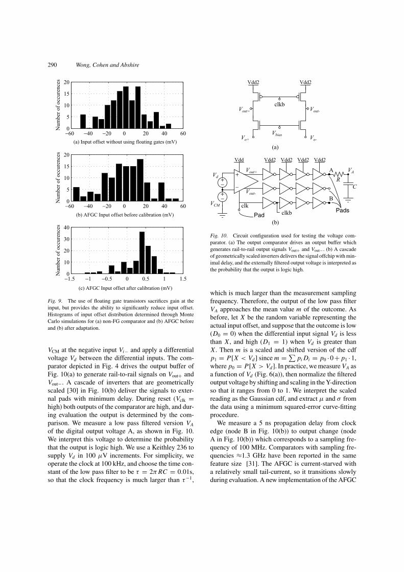
The circuit configuration used for testing the compara-tor is shown in Fig. 10. We bias the comparator with
290 Wong, Cohen and Abshire
−60 −40 −20 0 20 40 600
5
10
15
20
(a) Input offset without using floating gates (mV)
Num
ber
of o
ccur
ence
s
−60 −40 −20 0 20 40 600
5
10
15
20
(b) AFGC Input offset before calibration (mV)
Num
ber
of o
ccur
ence
s
−1.5 −1 −0.5 0 0.5 1 1.50
10
20
30
40
(c) AFGC Input offset after calibration (mV)
Num
ber
of o
ccur
ence
s
Fig. 9. The use of floating gate transistors sacrifices gain at theinput, but provides the ability to significantly reduce input offset.Histograms of input offset distribution determined through MonteCarlo simulations for (a) non-FG comparator and (b) AFGC beforeand (b) after adaptation.
VCM at the negative input Vi− and apply a differentialvoltage Vd between the differential inputs. The com-parator depicted in Fig. 4 drives the output buffer ofFig. 10(a) to generate rail-to-rail signals on Vout+ andVout−. A cascade of inverters that are geometricallyscaled [30] in Fig. 10(b) deliver the signals to exter-nal pads with minimum delay. During reset (Vclk =high) both outputs of the comparator are high, and dur-ing evaluation the output is determined by the com-parison. We measure a low pass filtered version VA
of the digital output voltage A, as shown in Fig. 10.We interpret this voltage to determine the probabilitythat the output is logic high. We use a Keithley 236 tosupply Vd in 100 µV increments. For simplicity, weoperate the clock at 100 kHz, and choose the time con-stant of the low pass filter to be τ = 2π RC = 0.01s,so that the clock frequency is much larger than τ−1,
+−
+− _
+
clk
Vout+
Vout-
Vdd Vdd2 Vdd2 Vdd2 Vdd2
PadsPad
RC
A VAVd
VCM
B
Vdd2 Vdd2
clkb
clkb
Vbias
Vout+
Vo+
Vout-
Vo-
(a)
(b)
Fig. 10. Circuit configuration used for testing the voltage com-parator. (a) The output comparator drives an output buffer whichgenerates rail-to-rail output signals Vout+ and Vout−. (b) A cascadeof geometrically scaled inverters delivers the signal offchip with min-imal delay, and the externally filtered output voltage is interpreted asthe probability that the output is logic high.
which is much larger than the measurement samplingfrequency. Therefore, the output of the low pass filterVA approaches the mean value m of the outcome. Asbefore, let X be the random variable representing theactual input offset, and suppose that the outcome is low(D0 = 0) when the differential input signal Vd is lessthan X , and high (D1 = 1) when Vd is greater thanX . Then m is a scaled and shifted version of the cdfp1 = P[X < Vd ] since m = ∑
pi Di = p0 ·0+ p1 ·1,where p0 = P[X > Vd ]. In practice, we measure VA asa function of Vd (Fig. 6(a)), then normalize the filteredoutput voltage by shifting and scaling in the Y-directionso that it ranges from 0 to 1. We interpret the scaledreading as the Gaussian cdf, and extract µ and σ fromthe data using a minimum squared-error curve-fittingprocedure.
We measure a 5 ns propagation delay from clockedge (node B in Fig. 10(b)) to output change (nodeA in Fig. 10(b)) which corresponds to a sampling fre-quency of 100 MHz. Comparators with sampling fre-quencies ≈1.3 GHz have been reported in the samefeature size [31]. The AFGC is current-starved witha relatively small tail-current, so it transitions slowlyduring evaluation. A new implementation of the AFGC

Differential Hot Electron Injection in an Adaptive Floating Gate Comparator 291
separates the input stages from the latch and introducesa modified output buffer to increase the speed [25].
4.1. Input Offset Distribution
We set Vdd to 4.5 V to allow injection and Vdd2 to 3.3 Vfor the output buffers. We raise VCM to 2.5 V (or higher)for programming, as demonstrated in the following ex-periments. We measure the offset for AFGC circuitson twelve different chips before any programming, af-ter UV erasure, and after programming. For unpro-grammed chips, the input offset has mean 45.35 mVand standard deviation of 73 mV. After 20 hours ofUV erasure, the mean offset is reduced to 22.02 mVwith a standard deviation of 6.37 mV. This means thata significant amount of random initial charge exists onthe floating gate when the chip is fabricated. We thencancel the offset by initiating injection on the p-typedifferential pair. After programming, the mean offsetis −109 µV with a standard deviation of σo = 379 µV.The maximum observed residual offset after adapta-tion was 728 µV. These results demonstrate more thantwo orders of magnitude reduction in offset voltage:relative to fabricated chips directly from the foundry,the mean is reduced by a factor of 416 and the varianceby a factor of 193; relative to UV-irradiated chips, themean is reduced by a factor of 202 and the variance by afactor of 17. Figure 11 shows the average offset beforeadaptation, after UV erasure, and after adaptation.
We infer the injection mismatch ratio (ρ) from themeasured input-referred noise (σn) and residual offset.The injection is performed with Vclk = 3.3 V, whichresults in input-referred noise σn ≈ 1.025 mV. We
raw UV Injected0
20
40
60
80
mV
meanstd
Fig. 11. Mean and standard deviation of input-referred offset mea-sured before adaptation (left), after UV erasure (middle), and afteradaptation (right).
calculate the injection mismatch ratio ρ according toEq. (2), and find that it has a mean value of 8.3% withstandard deviation 28% and maximum observed valueof 52.2%. Therefore, the pFET injection currents ex-hibit non-negligible variation among transistors.
4.2. Conversion Accuracy as a Functionof Clock Voltage
Figure 12 confirms that for lower clock voltages, i.e.lower voltage applied to the gate of M5 during the re-set phase, a finer comparison can be made on the inputsignal. The voltage gain in the p-type differential pairis increased by lowering the clock voltage, so the in-put offset can be adjusted with higher resolution at thecost of longer reset time and longer overall adaptation.If the clock voltage is too low (<2.1 V), reset will beincomplete, resulting in hysteresis in the comparisonoutcome and adaptation. We can avoid this problem bykeeping the clock voltage above a value defined by thenFET threshold. Experimentally we find that 742 µVis a lower-limit for the input-referred noise σn . This ex-ceeds the standard deviation of the input-referred off-set (post adaptation) σn > σo, which confirms that theinput-referred noise dominates resolution. Assumingthat the input signal has a 3.3 V peak-to-peak swing,σn = 742 µV translates into 63.9 dB SNR or equiva-lently, 10 effective bits in a single comparison. By av-eraging over several adaptation cycles we can reducethe contribution of circuit noise to reach the limitingresolution provided by the offset adaptation procedure(σo = 379 µV), which translates into 78.8 dB SNR
2 2.5 3 3.50.7
0.75
0.8
0.85
0.9
0.95
1
1.05
Clock voltage (V)
Inpu
t–re
ferr
ed n
oise
σn (
mV
)
Fig. 12. Conversion accuracy depends on the clock voltage Vclk.Accuracy increases with circuit gain as Vclk is reduced.

292 Wong, Cohen and Abshire
−1 −0.8 −0.6 −0.4 −0.2
−1.2
−1
8
6
−0.
−0.
−0.
4
−0.2
Programmed Input Offset (V)
Res
idua
l Inp
ut O
ffse
t (m
V)
Vcm,op=1.9VVcm,op=1.6V
Fig. 13. Residual input offset voltages remain small over a widerange of programmed offset voltages.
or 13 effective bits. In this experiment, we used a biascurrent of 40 µA, VCM of 1.2 V, Vdd of 4 V, and Vdd2
of 3.3 V, corresponding to a power consumption of160 µW.
4.3. Input-Referred Offsets Programmed Over±1 V Range
The AFGC can automatically cancel input offset, asshown above, or can be used to program a desired off-set over a wide range of input values. Figure 13 showsthe residual input offset voltages after programmingdifferent offsets ranging from −1 V to +1 V. These ex-periments used VCM = 2.5V for injection. The voltageresidue is defined to be the measured input offset minusthe programmed input offset. The solid trace shows theinput offsets measured for VCM = 1.9 V, and the dashedtrace shows the result when measured for VCM = 1.6 V.Larger shifts of VCM from injection conditions resultin larger offset errors during operation. This is causedby Early voltage mismatches on the p-type differentialpair and channel length modulation on the pFET thatprovides Ibias for the p-type differential pair.
4.4. Time Course of Offset Adaptation
Figure 14 shows the time course of adaptation. We firstintroduce a 0.2 V input offset on the gate, and then pulsethe VCM to an appropriate injection voltage (between3 and 3.3 V) for 10 ms (1000 clock cycles) with Vd =0 V and the clock running at a frequency of 100 kHz.We take measurements with VCM = 1.9 V between
0 0.2 0.4 0.6 0.8 1 1.2 1.4 1.6 1.8 2 2.20
50
100
150
200
Clock cycles × 104
Inpu
t off
set (
mV
)
VCM
=3.0VV
CM=3.1V
VCM
=3.2VV
CM=3.3V
Fig. 14. Input offset decreases exponentially in time. Offset is ini-tially 200 mV and decreases in time, with decay time constant in-creasing with VCM.
each pulse. We can see that for higher programmingVCM we achieve faster convergence. The time courseis roughly exponential, as predicted by the injectionmodel in Eq. (1). After the offset reaches 0 V it remainsthere, for all values of VCM.
Assuming that the input offset voltage µ decays ex-ponentially with injection time constant τ j from an ini-tial value µ0 = 200 mV, the input offset decays asµ(t) = µ0e−t/τ j . From the experimental data µ(t) wecan estimate τ j . The estimates are depicted as ‘+’s inFig. 15 as a function of VCM. The injection time con-stant ranges from 100 ms for VCM = 3 V to 18 ms forVCM = 3.3 V. The injection time constant decreases ex-ponentially with VCM, i.e. τ j (VCM) = τ j0e−k(VCM−Vth j ),which is consistent with our simple model of injection.The time constant τ j is inversely proportional to the in-jection current, which in turn is roughly exponential indrain to gate voltage. The gate-to-drain voltage scaleswith VCM, and Vth j is the “injection threshold voltage”.We fit the data in Fig. 15 with a dashed line correspond-ing to τ j0 = 1s, k = 6.43 and Vth j = 2.64V. Experi-mentally we find injection starting around VCM = 2.5Vwith adaptation occurring within seconds, confirmingthe accuracy of this simple exponential approximation.
4.5. Overshoot
The results described in previous sections have beenobtained using the dynamic adaptation method, witha running clock and injection occurring during the

Differential Hot Electron Injection in an Adaptive Floating Gate Comparator 293
3 3.1 3.2 3.30
0.02
0.04
0.06
0.08
0.1
VCM
Inje
ctio
n tim
e co
nsta
nt τ
j (s) Measured τ
jCurve–fitted τ
j
Fig. 15. Measured and inferred injection time constant τ j vs. VCM.
evaluation phase of operation. If we supply a constanthigh voltage at the clock terminal as occurs during thereset phase, the comparator becomes an amplifier withgain determined by the clock voltage. We perform staticinjection on the comparator in this amplifier configu-ration and observe the injection behavior. Figure 16shows an injection time course for a constant voltageof 3 V applied to the clock terminal. The setup is similarto the previous experiment (injection time course), butwith a higher Vdd (5.3 V) and a longer VCM pulse period(100 ms). As before, we program an initial input offsetof 0.2 V, and record the input offset once every 0.1sduring injection. As depicted in Fig. 16, the input off-set voltage does not stop when the offset reaches 0 V at
0 0.2 0.4 0.6 0.8 1–10
0
10
20
30
40
50
60
70
80
Time (s)
Inpu
t Off
set (
mV
)
Fig. 16. Input offset for the static injection method with clock heldconstantly high. Offset first decreases, then “overshoots” the desiredpoint and settles at a nonzero offset voltage.
time 0.4s, but rather continues to drop. This overshootphenomenon exists because the injection currents be-come unbalanced during programming. The injectioncurrents are proportional to the channel currents of thep-differential pair, and these currents are changing invalue due to the correction. Note that the equilibriumdoes not imply equal channel currents or equal out-put voltages, since injection depends on both channelcurrent and gate-drain voltage.
4.6. Temperature Dependence
To verify robustness of the AFGC, we measured theinput-referred offset voltage over a 20◦C temperaturerange. The test fixture is placed on a hot plate withsimple thermal insulation. A temperature sensor is at-tached to the top surface of the 40-pin DIP ceramic chippackage. The comparator is calibrated with 100 mV in-put offset at the two extreme temperatures, and input-referred offset error is measured at intermediate tem-peratures. First, we calibrate the comparator at 27.0◦C.The solid trace in Fig. 17 shows the residual input off-set measured as the temperature increases up to 50.0◦C.Next, we perform adaptation at 50.0◦C, and record theresidual input offset measures as the temperature de-creases down to 29.7◦C (dashed trace).
The accuracy of adaptation does not exhibit dis-cernible variation with temperature. When calibratedat temperatures of 27.0 and 50.0◦C, the error is
25 30 35 40 45 50−0.5
−0.4
−0.3
−0.2
−0.1
0
0.1
0.2
Off
set e
rror
(m
V)
Temperature ( ° C)
Inj @ 27 ° C
Inj @ 50 ° C
Fig. 17. Input offset voltage error of the AFGC measured over arange of temperatures from room temperature (27◦C) to 50◦C. Datais shown for a single comparator, first calibrated with an initial offsetof 100 mV at room temperature. As the temperature increases theoffset error decreases. Subsequently the comparator was calibratedwith an initial offset of 100 mV at 50◦C. As the temperature decreasesfrom 50◦C the offset error increases.

294 Wong, Cohen and Abshire
−222 and −204 µV, respectively. Once calibrated ata given temperature, however, the input-referred offsetdoes vary with temperature. From the data in Fig. 17,the temperature coefficient is roughly−15µV/◦C. Dif-ferential circuits are inherently tolerant to globally ap-plied perturbations, and consequently the temperaturedrift is more than two orders of magnitude less than−2.4 mV/◦C, the threshold voltage drift for an ordi-nary CMOS process [32].
4.7. Offset Charge Retention Time
While most of the measurements reported thus far (Sec-tions 4.1–4.6) have been obtained over relatively shorttime periods, the ability to program an offset voltagewhich is retained over an extended period of time ishighly desirable. We have confirmed experimentallythat the floating gate comparator accurately retains off-set for more than a month. Figure 18 shows residualinput offset measurements for two different chips, oneprogrammed initially with 0 V input offset, and oneprogrammed initially with 100 mV input offset. In be-tween each measurement, the chips are removed fromthe test fixture and stored on conductive foam. We per-form the measurements using standard ESD protectionbut no other special precautions.
0 200 400 600 800−0.9
−0.8
−0.7
−0.6
−0.5
−0.4
−0.3
−0.2
−0.1
0
Time (Hour)
Off
set e
rror
(m
V)
Inj with 100mVInj with 0V
Fig. 18. Residual input offset voltage error of the AFGC measuredover a 34-day period. Data is shown for two comparators, calibratedwith initial offsets of 0 V and 100 mV respectively. In between eachmeasurement the chips are removed from the test board and storedunder ordinary lab conditions. Measurements of the two comparatorsoccurred simultaneously, and systematic variation of the measuredoffsets is apparent. This variation is likely due to ambient temperaturefluctuations.
For the chip programmed with 100 mV, the errorstays around −450 µV. For the chip programmed with0 V, the offset drifted by 691 µV in the first 3 days,then stayed around −750 µV through the end of theexperiment. The initial drift is likely to be due to therelaxation mechanisms or to residual injection with theinputs at the common mode voltage used for evalua-tion. The drift stops in the fourth day. During the mea-surement period there is systematic variation observedon both chips; these variations are likely to be causedby ambient temperature fluctuations in the laboratorysetting.
5. Conclusion
In this paper we presented the technique of differ-ential hot electron injection for adapting and storingsigned state variables using floating gates. This ap-proach is compatible with all modern digital CMOStechnologies and can be readily extended to novelcircuit applications. The method has been previouslyreported in linear circuit architectures using nonlo-cal control of the adaptation. In this work we haveextended this method for a nonlinear circuit, whichprovides a highly compact and robust implementa-tion of a comparator. The technique takes advan-tage of impact-ionized hot electron injection currents,usually considered “undesirable” for submicron cir-cuit design, and uses them to improve circuit perfor-mance and reduce layout area rather than “fight” thephysics.
The adaptive floating gate comparator uses pFEThot-electron injection in a negative feedback loop dur-ing adaptation and programs nonvolatile correctivecharges on the floating gates. The load for the input dif-ferential pair is a regenerative element which computesthe outcome of the comparison and inherently presentsappropriate voltages for locally programming the in-put floating gate nodes. The technique is not limited tolocal adaptation and we are currently extending it forthe case of nonlocal adaptation which allows greaterflexibility in design.
Experiments show that adaptation consistently pro-duces residual offset which is a fraction of input-referred noise for all observed values of injection mis-match. We experimentally demonstrate more than twoorders of magnitude reduction in offset voltage: themean offset is reduced by a factor of 416 relative to

Differential Hot Electron Injection in an Adaptive Floating Gate Comparator 295
fabricated chips directly from the foundry and by afactor of 202 relative to UV-irradiated chips. The adap-tation encompasses the entire comparator circuitry andtherefore the residual offset is independent of initial de-vice offset. We consider both static and dynamic adap-tation and conclude that the the accuracy of offset can-cellation using the dynamic paradigm is approximatelytwo orders of magnitude better than the static paradigm.In the presence of observed 8% injection mismatch, theAFGC robustly converges to within 728 µV of the de-sired input offset (mean offset −109 µV, standard de-viation 379 µV). Offset cancellation is achieved withinmilliseconds. We report charge retention after adapta-tion for more than one month, and show that after adap-tation the variation of offset error with temperature is−15 µV/◦C, significantly less than the temperature co-efficient of typical MOS devices.
Acknowledgments
We thank the MOSIS service for providing chip fab-rication through their Educational Research Program.Y.L. Wong is supported by The Johns Hopkins Univer-sity Applied Physics Laboratory. P.A. Abshire is sup-ported by an NSF CAREER Award (0238061). Theauthors thank anonymous reviewers for their insightfulcomments.
References
1. T. Constandinou, J. Georgiou, and C. Toumazou, “An auto-input-offset removing floating gate pseudo-differential transconduc-tor,” in IEEE Int. Symp. Circuits Systems, May 2003, vol. 1, pp.169–172.
2. R. Chawla, G. Serrano, D. Allen, A. Pereira, and P. Hasler,“Fully differential floating-gate programmable OTAs with novelcommon-mode feedback,” in IEEE Int. Symp. Circuits Systems,May 2004, vol. 1, pp. I–817–820.
3. P. Hasler, P. Smith, C. Duffy, C. Gordon, J. Dugger, and D.Anderson, “A floating-gate vector-quantizer,” in Proc. IEEEMidwest Symp. Circuits and Syst, Aug. 2002, vol. 1, pp. I-196–199.
4. P. Hasler, B. Minch, and C. Diorio, “An autozeroing floating-gate amplifier,” IEEE Trans. Circuits Syst. II, vol. 48, no. 1, pp.74–82, 2001.
5. J. Hyde, T. Humes, C. Diorio, M. Thomas, and M. Figueroa, “A300-MS/s 14-bit digital-to-analog converter in logic CMOS,”IEEE J. Solid-State Circuits, vol. 38, no. 5, pp. 734–740, 2003.
6. J. Dickson, “On-chip high-voltage generation in NMOS in-tegrated circuits using an improved voltage multiplier tech-nique,” IEEE J. Solid-State Circuits, vol. 11, no. 3, pp. 374–378,1976.
7. J. Xiao, A. Peterchev, J. Zhang, and S. Sanders, “An ultra-low-power digitally-controlled buck converter IC for cellular phoneapplications,” in Proc. IEEE Appl. Power Electron. Conf., 2004,vol. 1, pp. 383–391.
8. C. A. Mead, “Adaptive retina,” in Analog VLSI Implementationsof Neural Systems. Kluwer, Norwell, MA, 1989.
9. Y. Berg, T.S. Lande, and Ø. Næss, “Programming floating-gatecircuits with UV-activated conductances,” IEEE Trans. CircuitsSyst. II, vol. 48, no. 1, pp. 12–19, 2001.
10. P. Pouliquen, A. Andreou, K. Strohbehn, and R. Jenkins, “An as-sociative memory integrated system for character recognition,”in Proc. IEEE Midwest Symp. Circuits and Syst, Aug. 1993,vol. 1, pp. 762–765.
11. K. Boahen, P. Pouliquen, A. Andreou, and R. Jenkins, “A het-eroassociative memory using current-mode MOS analog VLSIcircuits,” IEEE Trans. Circuits Syst., vol. 36, no. 5, pp. 747–755,1989.
12. J. Lubkin and G. Cauwenberghs, “VLSI implementation of fuzzyadaptive resonance and learning vector quantization,” Int. J. Ana-log Integrated Circuits and Signal Processing, vol. 30, no. 2, pp.149–157, 2002.
13. O. Rossetto, C. Jutten, J. Herault, and I. Kreuzer, “Analog VLSIsynaptic matrices as building blocks for neural networks,” IEEEMicro, vol. 9, no. 6, pp. 56–63, 1989.
14. M. Cohen and A. Andreou, “Current-mode subthreshold MOSimplementation of the Herault-Jutten autoadaptive network,”IEEE J. Solid-State Circuits, vol. 27, no. 5, pp. 714–727,1992.
15. P. Hasler and J. Dugger, “Correlation learning rule in floating-gate pFET synapses,” IEEE Trans. Circuits Syst. II, vol. 48, no. 1,pp. 65–73, 2001.
16. P. Hasler, “Continuous-time feedback in floating-gate MOS cir-cuits,” IEEE Trans. Circuits Syst. II, vol. 48, no. 1, pp. 56–64,January 2001.
17. K. Rahimi, C. Diorio, C. Hernandez, and M. Brockhausen, “Asimulation model for floating-gate MOS synapse transistors,” inIEEE Int. Symp. Circuits Systems, May 2002, vol. 2, pp. 532–535.
18. E. Rosenbaum, R. Rofan, and C. Hu, “Effect of hot-carrier injec-tion on n- and pMOSFET gate oxide integrity,” IEEE ElectronDevice Letters, vol. 12, no. 11, pp. 599–601, 1991.
19. B. Kaczar, R. Degraeve, G. Groeseneken, M. Rasras, S. Kubicek,E. Vandamme, and G. Badenes, “Effect of hot-carrier injectionon n- and pMOSFET gate oxide integrity,” in IEDM TechnicalDigest, 2000, pp. 553–556.
20. T. Yamasaki and T. Shibata, “Analog soft-pattern-matching clas-sifier using floating-gate MOS technology,” IEEE Trans. NeuralNetworks, vol. 14, no. 5, pp. 1257–1265, 2003.
21. P. Abshire, E. Wong, Y. Zhai, and M. Cohen, “Adaptive logdomain filters using floating gate transistors,” in IEEE Int. Symp.Circuits Systems, May 2004, vol. 1, pp. I-29–32.
22. M. Cohen, R. Edwards, G. Cauwenberghs, M. Vorontsov, andG. Carhart, “AdOpt: Analog VLSI stochastic optimization foradaptive optics,” in Int. Joint Conf. Neural Networks, July 1999,vol. lxii+4439, pp. 762–765.
23. R. Harrison, J. Bragg, P. Hasler, B. Minch, and S. Deweerth, “ACMOS programmable analog memory-cell array using floating-gate circuits,” IEEE Trans. Circuits Syst. II, vol. 48, no. 1, pp.4–11, 2001.

296 Wong, Cohen and Abshire
24. M. Hooper, M. Kucic, and P. Hasler, “5 V-only, standard .5 µmCMOS programmable and adaptive floating-gate circuits andarrays using CMOS charge pumps,” in IEEE Int. Symp. CircuitsSystems, May 2004, vol. 5, pp. 832–835.
25. E. Wong, P. Abshire, and M. Cohen, “A 1.2 GHz adaptive floatinggate comparator with 13-bit resolution,” to appear in IEEE Int.Symp. Circuits Systems, May 2005.
26. B. Razavi and B. Wooley, “Design techniques for high-speed,high-resolution comparators,” IEEE J. Solid-State Circuits,vol. 27, no. 12, pp. 1916–1926, 1992.
27. M. Cohen and G. Cauwenberghs, “Floating-gate adaptation forfocal-plane online nonuniformity correction,” IEEE Trans. Cir-cuits Syst. II, vol. 48, no. 1, pp. 83–89, 2001.
28. S. Shah and S. Collins, “A temperature independent trimmablecurrent source,” in IEEE Int. Symp. Circuits Systems, May 2002,vol. 1, pp. I713–I716.
29. S. Jackson, J. Killens, and B. Blalock, “A programmable cur-rent mirror for analog trimming using single poly floating-gatedevices in standard CMOS technology,” IEEE Trans. CircuitsSyst. II, vol. 48, no. 1, pp. 100–102, 2001.
30. R. Jaeger, “Comments on ‘An optimized output stage for MOSintegrated circuits’,” IEEE J. Solid-State Circuits, vol. SC-10,no. 1, pp. 185–186, 1975.
31. M. Choi and A. Abidi, “A 6-b 1.3-Gsample/s A/D converter in0.35 µm CMOS,” IEEE J. Solid-State Circuits, vol. 36, no. 12,pp. 1847–1858, 2001.
32. R.J. Baker, H.W. Li, and D.E. Boyce, CMOS Circuit Design,Layout, and Simulation. Piscataway, NJ, Wiley–IEEE Press,1997.
Yanyi Liu Wong received the B.S. and M.S. de-grees in Electrical Engineering in 2001 and 2004, re-spectively, from the University of Maryland, CollegePark, where he is currently working toward the Ph.D.degree. From 2001 to 2003, he was a Teaching As-sistant for microelectronics lectures and labs. Since2003, he has been with The Johns Hopkins Univer-sity Applied Physics Laboratory developing Radiation-Hardened-By-Design EEPROM subsystems for spacebased ASICs. At the same time, he has been workingas a Research Assistant at the Integrated BiomorphicInformation Systems Laboratory, UMCP, and has beenactively designing low-power, mixed-signal, adaptivefloating gate circuits and applications in commerciallyavailable CMOS processes.
Marc H. Cohen received both B.Sc. and M.Sc. de-grees in Electrical Engineering from the University ofthe Witwatersrand, Johannesburg, South Africa in 1978and 1983 respectively. He received an M.S. in Biomedi-cal Engineering and a Ph.D. in Electrical and ComputerEngineering from The Johns Hopkins University, Bal-timore, MD, USA in 1991 and 2001 respectively. Heis currently an Assistant Research Scientist in the In-stitute for Systems Research, University of Maryland,College Park. His research interests lie in the areas ofadaptive low power analog and mixed-signal integratedcircuit design. Current application areas include ultra-sonic echolocation, contact imagers for control of mi-crofluidic devices, controllers for adaptive optics andintegrated sensors for RFID.
Pamela A. Abshire received the B.S. degree inphysics with honor in 1992 from the California Instituteof Technology. Between 1992 and 1995 she worked asa Research Engineer in the Bradycardia Research De-partment of Medtronic, Inc. She received her M.S. andPh.D. degrees in Electrical and Computer Engineer-ing from The Johns Hopkins University in 1997 and2002, respectively. She is currently an assistant pro-fessor in the Department of Electrical and ComputerEngineering and the Institute for Systems Research atthe University of Maryland, College Park. Dr. Abshire’sresearch focuses on low power mixed signal integratedcircuit design, adaptive integrated circuits, integratedcircuits for biosensing, and understanding the trade-offs between performance and energy in natural andengineered systems.