dielectric loaded antennas - eefocusdata.eefocus.com/myspace/0/942/bbs/1174163529/56531463.pdf ·...
TRANSCRIPT

DIELECTRIC LOADED ANTENNAS
L. SHAFAI
University of ManitobaWinnipeg, Manitoba, Canada
1. INTRODUCTION
A transmit antenna converts the energy of a guided wavein a transmission line into the radiated wave in anunbounded medium. The receive antenna does the re-verse. The transmission lines such as waveguides andcoaxial and microstrip lines use conductors mostly toconfine and guide the energy, but antennas use them toradiate it. Because the radiated energy is in unboundedregion, phase control is often used to direct the radiationin the desired direction. Dielectrics play an important rolein this process, and this article discusses a few represen-tative cases. An important antenna parameter is itsdirectivity, which is the measure of its control over theenergy flow. To increase the directivity, the antenna sizemust be increased, and the influence of dielectrics on theirperformance changes considerably. Thus, in this article,the use of dielectrics in antenna applications is dividedinto two categories of large high-gain and small low-gainantenna applications.
In high-gain antenna applications, reflectors andlenses are used extensively [1]. They are passive andoperate principally on the basis of their geometry. Conse-quently, they are relatively low-cost, reliable, and wide-band. Reflectors are usually made of good conductors, andthus have lower loss, and because of their high strength,can be made light. But reflectors suffer from limited scancapability. Lenses, on the other hand, because of theirtransparency, have more degree of freedom, specifically,two reflecting surfaces and the relative permittivity orrefractive index. They also do not suffer from apertureblockage. However, lenses have disadvantages in largevolume and high weight.
In microwave antenna applications, lenses have nu-merous and diverse applications, but in most cases theyare large in size with respect to wavelength. Thus, physi-cal and geometric optics apply, and most of the lens designtechniques can be adopted from optics to microwaveapplications. The aperture theory and synthesis techni-ques can also be used effectively to facilitate designs. Inaddition, the use of an optical ray path in lens designmakes the solution frequency-independent. In practice,however, the lens size in microwave frequencies is finitewith respect to the wavelength, and the feed antenna isfrequency-sensitive. Thus, the performance of the lensantenna also becomes frequency-dependent.
Natural dielectrics at microwave frequencies have re-flective indices larger than unity and for collimation,require convex surfaces. However, artificial media usingguiding structures, such as waveguides, are equivalent to
dielectrics with refractive index less than unity, and resultin concave lenses. They are usually dispersive, resultingin variation of the refractive index with frequency, andhave narrower operating bandwidths.
In small antennas dielectrics are used often to improvethe radiation efficiency and polarization of the antennas,such as waveguides and horns. This is important intelecommunication applications, where polarization con-trol is required to implement frequency reuse and mini-mize interference, especially in satellite and wirelesscommunications. Horn antennas and reflector feeds areexamples that incorporate dielectrics or lens loading toimprove performance [2].
Another area of important dielectric use is insulatedantennas in biological applications and remote sensingwith buried or submerged antennas. The use of dielectricloading eliminates direct RF energy leak into the lossyenvironments, and ensure radiative coupling into thetarget objects. Often a full-wave analysis is needed toprovide a proper understanding of their resonance prop-erty and coupling mechanism to the surrounding media.
The dielectric loading is also used for antenna minia-turization. Low-loss dielectrics with medium to high re-lative permittivities are now available and are usedincreasingly to reduce the antenna size. A number ofimportant areas include dielectric-loaded waveguidesand horn, and dielectric resonator and microstrip anten-nas. By aperture loading of waveguides and small horns,excellent pattern symmetry and low cross-polarizationcan be obtained, which are essential features of reflectorand lens feeds. In addition, the dielectric loading reducesthe size of the antennas and makes them useful candi-dates for multibeam applications, using reflectors andlenses. Miniaturization of the antenna is also an impor-tant requirement in wireless communications. Microstrippatch or slot antennas with high-relative-permittivitysubstrates play an important role in this area, and theirderivatives are used in most applications. In dipole andmonopole cases the dielectric loading is external and usedfor size reductions.
Finally, dielectric loading can also be used for gainenhancement, without shaping them such as lenses. Pla-nar dielectrics can be used as radomes or covers to protectthe antennas. By proper selection of the radome para-meters, the antenna gain can also be increased signifi-cantly, while protecting the antennas from theenvironment.
2. DIELECTRIC LENS ANTENNAS
In optical terms, a lens produces an image of a sourcepoint at the image point, and lenses could be locatedanywhere in the space. As an antenna, this propertymeans that the source and image points are focused ateach other and the lens has two focal points. In turn, thesefocal points signify locations in the space, where raysemanating from the lens arrive at equal phases. This
D
893
property provides a mathematical relationship for describ-ing the lens operation, and therefore its design.
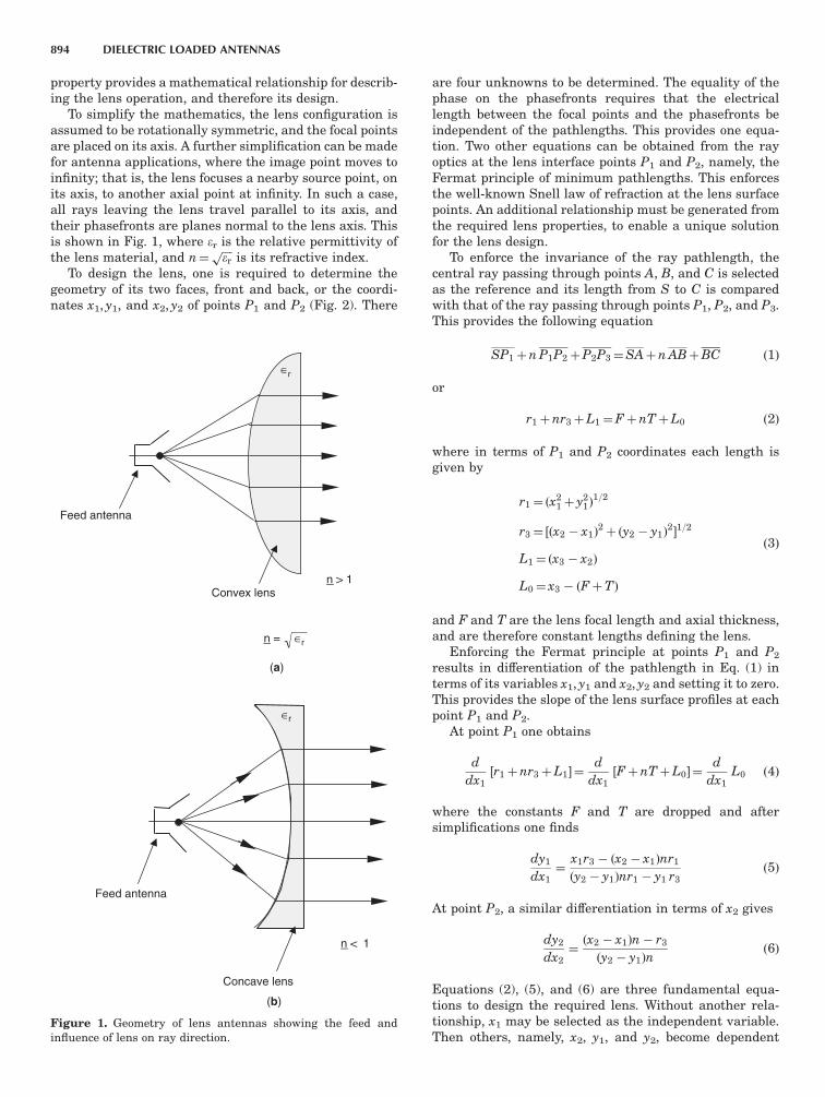
To simplify the mathematics, the lens configuration isassumed to be rotationally symmetric, and the focal pointsare placed on its axis. A further simplification can be madefor antenna applications, where the image point moves toinfinity; that is, the lens focuses a nearby source point, onits axis, to another axial point at infinity. In such a case,all rays leaving the lens travel parallel to its axis, andtheir phasefronts are planes normal to the lens axis. Thisis shown in Fig. 1, where er is the relative permittivity ofthe lens material, and n¼
ffiffiffiffi
erp
is its refractive index.To design the lens, one is required to determine the
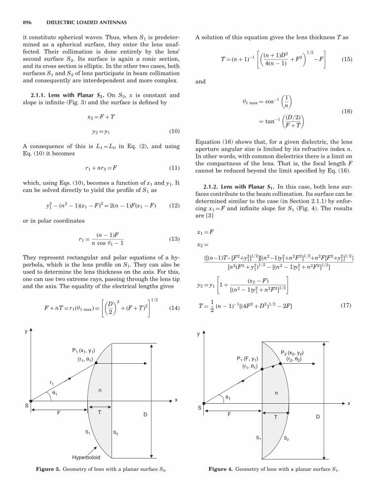
geometry of its two faces, front and back, or the coordi-nates x1, y1, and x2, y2 of points P1 and P2 (Fig. 2). There
are four unknowns to be determined. The equality of thephase on the phasefronts requires that the electricallength between the focal points and the phasefronts beindependent of the pathlengths. This provides one equa-tion. Two other equations can be obtained from the rayoptics at the lens interface points P1 and P2, namely, theFermat principle of minimum pathlengths. This enforcesthe well-known Snell law of refraction at the lens surfacepoints. An additional relationship must be generated fromthe required lens properties, to enable a unique solutionfor the lens design.
To enforce the invariance of the ray pathlength, thecentral ray passing through points A, B, and C is selectedas the reference and its length from S to C is comparedwith that of the ray passing through points P1, P2, and P3.This provides the following equation
SP1þn P1P2þP2P3¼SAþn ABþBC ð1Þ
or
r1þnr3þL1¼FþnTþL0 ð2Þ
where in terms of P1 and P2 coordinates each length isgiven by
r1¼ðx21þ y2
1Þ1=2
r3¼ ½ðx2 x1Þ2þ ðy2 y1Þ
21=2
L1¼ ðx3 x2Þ
L0¼ x3 ðFþTÞ
ð3Þ
and F and T are the lens focal length and axial thickness,and are therefore constant lengths defining the lens.
Enforcing the Fermat principle at points P1 and P2
results in differentiation of the pathlength in Eq. (1) interms of its variables x1, y1 and x2, y2 and setting it to zero.This provides the slope of the lens surface profiles at eachpoint P1 and P2.
At point P1 one obtains
d
dx1r1þnr3þL1½ ¼
d
dx1FþnTþL0½ ¼
d
dx1L0 ð4Þ
where the constants F and T are dropped and aftersimplifications one finds
dy1
dx1¼
x1r3 ðx2 x1Þnr1
ðy2 y1Þnr1 y1 r3ð5Þ
At point P2, a similar differentiation in terms of x2 gives
dy2
dx2¼ðx2 x1Þn r3
ðy2 y1Þnð6Þ
Equations (2), (5), and (6) are three fundamental equa-tions to design the required lens. Without another rela-tionship, x1 may be selected as the independent variable.Then others, namely, x2, y1, and y2, become dependent
Feed antenna
Convex lens
∈r
n > 1
n = ∈r
Feed antenna
Concave lens
∈r
n < 1
(a)
(b)
Figure 1. Geometry of lens antennas showing the feed andinfluence of lens on ray direction.
894 DIELECTRIC LOADED ANTENNAS

variables to be determined in terms of x1. The solutionsgive the lens profiles in rectangular coordinates. If thelens profiles in polar coordinates are required, Eqs. (2), (5),and (6) can be obtained in terms of r1,y1 and r2,y2, thepolar coordinates of P1 and P2. Differentiating Eq. (2) interms of y1 and y2 gives
dr1
dy1¼
nr1r2 sinðy2 y1Þ
r3 n½r2 cosðy2 y1Þ r1ð7Þ
and
dr2
dy2¼
nr1r2 sinðy2 y1Þþ r2r3 sin y2
r3 sin y2 n½r2 r1 cosðy2 y1Þð8Þ
where use is made of the following polar coordinaterelationships:
x1¼ r1 cos y1
y1¼ r1 sin y1
x2¼ r2 cos y2
y2¼ r2 sin y2
r3¼ jr1 r2j ¼ ½r21þ r2
2 2r1r2 cosðy2 y1Þ1=2
ð9Þ
Solutions of Eqs. (7) and (8) give the lens profiles in polarcoordinates, which are often more compact in form. Also,for some simple lens configurations, they result in well-
known and easily recognizable parametric equations ofthe conic sections, generalizing the solution.
2.1. Examples of Simple Lenses
The lens design becomes considerably easier, if one of thelens surfaces is predetermined. This eliminates one of thedifferential equations, as the surface profile is alreadyknown. Among many surfaces to select the simpler onesare the planar and spherical surfaces, with the planarnormal to the lens axis. Such selections give simple profileequations. The planar surface is described by a constantx coordinate and the spherical one by a constant polarcoordinate r. These simplifications also assist in solutionsof the other lens profile, for which an analytic solution canalso be determined. Since either of the lens profiles can bepredetermined as planar or spherical, four possible solutionsexist. Only two, however, result in simple conical sections.
If the second surface S2 is assumed to be planar, normalto the lens axis, the rays arriving from the right-hand side,parallel to the lens axis x, enter the lens unaffected andchange direction only after the first lens surface S1. Thenthey focus at S; that is, only the S1 surface of the lenscollimates the beam. Looking from the left side, sphericalrays originating from the focal point S, enter the lens at S1
and become parallel to its axis. Thus, after leaving the lensat S2, since they are normal to S2, their direction remainsunchanged. In this case, the active surface S1 of the lens isa hyperbola in cylindrical lens, and hyperboloid in rota-tionally symmetric lens.
If the surface S1 is spherical, it becomes inactive, sincethe focal point is a point source and rays emanating from
(r1, θ1)
S1 S2
r1
θ1θ2
Phase front
P2 (x2, y2)
F
S
y
CA
T
x
D
B∈r,n
Sourcepoint
P1 (x1, y1) (r2, θ2)
(X3, 0)
r2
r3
L1
L0
P3
Figure 2. Geometry of a lens indicatingray and surface coordinates.
DIELECTRIC LOADED ANTENNAS 895
it constitute spherical waves. Thus, when S1 is predeter-mined as a spherical surface, they enter the lens unaf-fected. Their collimation is done entirely by the lens’second surface S2. Its surface is again a conic section,and its cross section is elliptic. In the other two cases, bothsurfaces S1 and S2 of lens participate in beam collimationand consequently are interdependent and more complex.
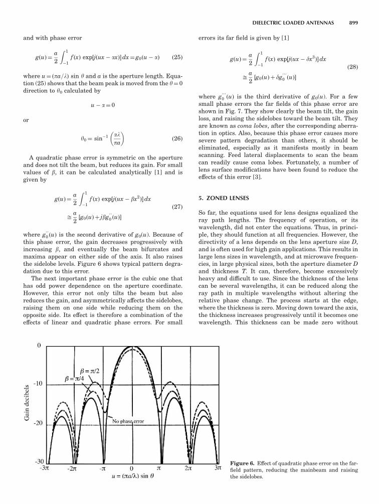
2.1.1. Lens with Planar S2. On S2, x is constant andslope is infinite (Fig. 3) and the surface is defined by
x2¼FþT
y2¼ y1 ð10Þ
A consequence of this is L1¼L0 in Eq. (2), and usingEq. (10) it becomes
r1þnr3¼F ð11Þ
which, using Eqs. (10), becomes a function of x1 and y1. Itcan be solved directly to yield the profile of S1 as
y21 ðn
2 1Þðx1 FÞ2¼ 2ðn 1ÞFðx1 FÞ ð12Þ
or in polar coordinates
r1¼ðn 1ÞF
n cos y1 1ð13Þ
They represent rectangular and polar equations of a hy-perbola, which is the lens profile on S1. They can also beused to determine the lens thickness on the axis. For this,one can use two extreme rays, passing through the lens tipand the axis. The equality of the electrical lengths gives
FþnT¼ r1ðy1 maxÞ¼D
2
2
þ ðFþTÞ2
" #1=2
ð14Þ
A solution of this equation gives the lens thickness T as
T¼ðnþ 1Þ1 ðnþ 1ÞD2
4ðn 1ÞþF2
1=2
F
" #
ð15Þ
and
y1 max¼ cos1 1
n
¼ tan1 ðD=2Þ
FþT
ð16Þ
Equation (16) shows that, for a given dielectric, the lensaperture angular size is limited by its refractive index n.In other words, with common dielectrics there is a limit onthe compactness of the lens. That is, the focal length Fcannot be reduced beyond the limit specified by Eq. (16).
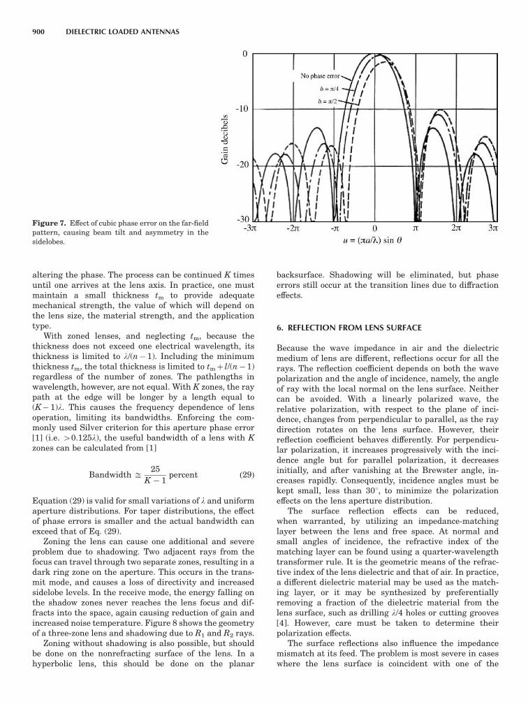
2.1.2. Lens with Planar S1. In this case, both lens sur-faces contribute to the beam collimation. Its surface can bedetermined similar to the case (in Section 2.1.1) by enfor-cing x1¼F and infinite slope for S1 (Fig. 4). The resultsare [3]
x1¼F
x2¼
f½ðn1ÞT½F2þy21
1=2½ðn21Þy21þn2F21=2þn2F½F2þy2
11=2g
½n2ðF2þ y21Þ
1=2 ½ðn2 1Þy2
1þn2F21=2
y2¼ y1 1þðx2 FÞ
½ðn2 1Þy21þn2F21=2
" #
T¼1
2ðn 1Þ1
½ð4F2þD2Þ1=2 2F ð17Þ
x
D
n
y
SF T
θ1
r1
S1 S2
Hyperboloid
(r1, θ1)
P1 (x1, y1)
Figure 3. Geometry of lens with a planar surface S2.
x
y
D
n
SF T
θ1
S1 S2
(r1, θ1)P1 (F, y1) (r2, θ2)
P2 (x2, y2)
Figure 4. Geometry of lens with a planar surface S1.
896 DIELECTRIC LOADED ANTENNAS

Note that, since the beam collimation is due to bothsurfaces, the coordinates of S2 are now dependent on thoseof S1.
2.1.3. Lens with One Spherical Surface. When S1 is aspherical surface, all spherical wave originating at thefocal point S pass through it unaffected. The second sur-face, S2, collimates the beam. The geometry is shown inFig. 5, and S2 is an ellipse given as
r2¼ðn 1ÞR
n cos y2ð18Þ
where R¼FþT and other parameters are as defined inFig. 5. Its equation in rectangular coordinates has the form
y2¼x2þ ðn 1ÞR
n
2
x22
" #1=2
and
T¼1
2ðn 1Þ1
½2F ð4F2 D4Þ1=2 ð19Þ
y2 max¼ cos1 1
n
the last equation again sets a limit for the peak angularaperture of the lens for a given dielectric material.
When the surface S2 is assumed to be spherical, thenboth lens surfaces participate in collimating the beam.The inner surface S1 can be obtained from [3]
n2½r22þ r2
1 2r1r2 cosðy1 y2Þ ¼ ½ðn 1ÞTþ r2 cos y2 r12
n2r1 sinðy1 y2Þ¼ sin y2½ðn 1ÞTþ r2 cos y2 r1 ð20Þ
T¼4ðn 1ÞF2 ðn 3ÞD2
4ðn 1Þðn 3Þ2
1=2
þF
n 3
3. EFFECT OF LENS ON AMPLITUDE DISTRIBUTION
The lens equations (1) to (6) were based on the ray pathanalysis, or in antenna terms, the phase relationships.The amplitude distributions were not considered. In prac-tical applications, however, the amplitude distributionsare also important and will influence the aperture effi-ciency of the lens, sidelobe levels, and cross-polarization.To state it briefly, a uniform aperture distribution givesthe highest directivity, but has high sidelobes because ofits high edge illumination. Sidelobes can be reduced bytapering the field toward the edge. Excessive tapering,however, rapidly reduces the lens directivity. It is there-fore useful to know the influence of the lens on the fieldamplitude as well.
Assume that A(y) is the angular dependence of thewave amplitude radiating from the focal points and A(r),with r¼ r sin y, the amplitude distribution of the colli-mated beam. Then, using the conservation of power, andneglecting the reflection at the lens surface, the followingamplitude relationships can be obtained [1].
Hyperbolic lens of case in Section 2.1.1
AðrÞAðy1Þ
¼1
F
ðn cos y1 1Þ3
ðn 1Þ2ðn cos y1Þ
" #1=2
ð21Þ
Elliptic lens of case in Section 2.1.3
AðrÞAðy1Þ
¼1
F
ðn cos y1Þ3
ðn 1Þ2ðn cos y1 1Þ
" #1=2
ð22Þ
An inspection of these equations shows that in Eq. (21) theamplitude ratio decreases with y1; that is, after leavingthe lens the field is concentrated near its axis. Theamplitude, in fact, drops to zero at the angle y1 max, givenby Eq. (16). This lens, therefore, enhances the field taperof the source and is a good candidate for low-sidelobeapplications. However, its aperture efficiency will be low.In contrast, the amplitude ratio in Eq. (22) increases with y1;that is, this lens corrects the amplitude taper of the sourceand enhances the aperture efficiency, but in the process,raises the sidelobe levels. Thus, it may be used in applica-tions in which the aperture efficiency is more critical thanthe sidelobe levels.
For most common dielectrics the refractive index isn¼ 1.6, (i.e., er ffi 2:55). For these materials the limit of theaperture angle is y1 max¼ 51.31. Within this limit theamplitude ratios of Eqs. (21) and (22), normalized to axialvalues, are shown in Table 1. The amplitude tapering ofhyperbolic lenses is clearly evident. A 351 lens addsanother 10 dB to the aperture field taper, and beyond401, the lens is practically useless. For large-angle-lensapplications, higher-dielectric-constant materials must beused. Table 1 also shows the amplitude enhancement ofelliptic lens. A 351 lens improves the aperture field uni-formity by as much as 6.3 dB. It increases rapidly there-after and yields about 10 and 20 dB improvements for lensangles of 451 and 501, respectively. These amplitudeenhancements, however, must be accepted as theoretical
S x
D
n
T
S
y
F
θ1
Spherical
S1
S2
(F, θ1)P1 (x1, y1)
(r2, θ2)P2 (x2, y2)
Figure 5. Geometry of lens with a spherical surface S1.
DIELECTRIC LOADED ANTENNAS 897

limits, since at these wide angles the lens surfacereflectivity will reduce the practically attainable levels.Surface matching layers must be used to minimize thereflections.
3.1. General Lens Design
In the general lens of Fig. 2, both surfaces are profiled andparticipate in collimating the beam. Thus, a more versa-tile lens can be obtained. However, Eqs. (1)–(6) showedthat there are at least four unknown coordinates, x1, y1
and x2, y2, to be determined. But, the optical relationshipsprovided only three equations, which are not sufficient todetermine uniquely the coordinates of both surfaces S1
and S2. Another relationship must be generated, whichmay be imposed on the amplitude distribution A(r), tocontrol the directivity or sidelobes. Alternatively, one mayimpose conditions on the aperture phase errors. An im-portant case is the reduction of phase errors due to thesource lateral defocusing. This will allow beam scanningwithout excessive degradation in efficiency and sidelobelevels. In most cases, however, the problem is too complexfor analytic solution and a numerical approval must beused.
4. ABERRATIONS
The term aberration, which originated in optics, refers tothe imperfection of lens in reproduction of the originalimage. In antenna theory, the performance is measured interms of the aperture amplitude and phase distributions.The phase distribution, however, is the most criticalparameter and influences the far field significantly. It istherefore used in evaluating the performance of apertureantennas such as lenses and reflectors. With a perfect lensand a point source at its focus, the phase error should notexist. However, there are fabrication tolerances, and mis-alignments can occur that will contribute to aberrations.Even without such imperfections, lens antennas can sufferfrom aberrations. Practical lens feeds are horn antennasand small arrays. Both have finite sizes and deviate fromthe point source [2]. This means that part of the feedaperture falls outside the focal point, and rays emanatingfrom them do not satisfy the optical relationships. Thus,on the lens aperture, the phase distribution is not uni-form. Similar situations also occur when the feed is movedoff axis laterally to scan the beam. Again, aperture phaseerror occurs as a result of pathlength differences. A some-what different situation arises when the feed is moved
axially, front or back. In this case, the phase error issymmetric, as all the rays leaving the source with equalangles travel equal distances and arrive at the aperture atan equal radial distance from the axis, that is, on acircular ring. But the length of the ray increases, ordecreases, with radial distance on the aperture. The phaseerror is, therefore, quadratic on the aperture and reducesthe aperture efficiency, while raising the sidelobes.
The general aberration (i.e., the lens aperturephase error) can depend implicitly on both feed andlens coordinates and be difficult to comprehend.However, like all other phase-error-related problems, itcan also be represented as the pathlength difference witha reference ray. For rotationally symmetric rays, thenatural reference is the axial ray. The pathlength differ-ence can then be obtained by a Taylor-type expansion ofthe general ray length in terms of the axial one. For smallaberrations the first few terms in the expansion will besufficient to describe the length accurately. In terms of theaperture polar coordinates r and f, the expansionbecomes
Lðr;fÞ¼Laxialþ ar cos fþ br2½1þ cos2 f þ gr3 cos fþ
ð23Þ
where a, b, and g are constants indicating the magnitudeof each phase error. The leading term is linear in r and f,then becomes quadratic, cubic, and so on, and the magni-tude of each depends on the nature of imperfection caus-ing the phase error. The even terms are caused by eitheran axial defocusing or an axially symmetric error. The oddterms can be due to a lateral displacement of the feed, orasymmetric errors.
The effects of each error can be investigated by itsintroduction in the aperture field and determining the farfield using a Fourier transformation or diffraction inte-gral. For one-dimensional errors (i.e., r¼ x and f¼ 0), theeffect can be understood easily, and has been investigatedby Silver [1]. The first term is linear and in a Fourierintegral shifts, the transform variable. It thus causes a tiltof the beam, but the gain remains the same. Using Silver’snotation, if f ðxÞ is the aperture distribution and g(u) thefar field, that is, its Fourier transform with a linear phaseerror, one finds, with no phase error
g0ðuÞ¼a
2
Z 1
1f ðxÞ exp½juxdx ð24Þ
Table 1. Amplitude Distributionsa for the Hyperbolic and Elliptic Lenses of Figs. 3 and 5
Amplitude ratioAðrÞAðy1Þ
Ray Angle y1 (degrees)
0 10 20 30 35 40 45 50
Hyperbolic lens equation [Eq. (21)] Relative value (dB) 1.0 0.928 0.733 0.466 0.328 0.196 0.084 0.0080.0 0.65 2.70 6.64 9.70 14.17 21.5 41.75
Elliptic lens equation [Eq. (22)] Relative value (dB) 1.0 1.060 1.26 1.69 2.06 2.67 3.17 9.250.0 0.51 2.01 4.55 6.29 8.54 10.03 19.33
aWhere n¼ 1.6, er¼ 2.55, y1 max¼ 51.31.
898 DIELECTRIC LOADED ANTENNAS
and with phase error
gðuÞ¼a
2
Z 1
1f ðxÞ exp½jðux axÞdx¼g0ðu aÞ ð25Þ
where u¼ ðpa=lÞ sin y and a is the aperture length. Equa-tion (25) shows that the beam peak is moved from the y¼ 0direction to y0 calculated by
u a¼ 0
or
y0¼ sin1 alpa
ð26Þ
A quadratic phase error is symmetric on the apertureand does not tilt the beam, but reduces its gain. For smallvalues of b, it can be calculated analytically [1] and isgiven by
gðuÞ¼a
2
Z 1
1f ðxÞ exp½jðux bx2Þdx
ffia
2½g0ðuÞþ jbg
0 0
0 ðuÞ
ð27Þ
where g0 0
0 ðuÞ is the second derivative of g0(u). Because ofthis phase error, the gain decreases progressively withincreasing b, and eventually the beam bifurcates andmaxima appear on either side of the axis. It also raisesthe sidelobe levels. Figure 6 shows typical pattern degra-dation due to this error.
The next important phase error is the cubic one thathas odd power dependence on the aperture coordinate.However, this error not only tilts the beam but alsoreduces the gain, and asymmetrically affects the sidelobes,raising them on one side while reducing them on theopposite side. Its effect is therefore a combination of theeffects of linear and quadratic phase errors. For small
errors its far field is given by [1]
gðuÞ¼a
2
Z 1
1f ðxÞ exp½jðux dx3Þdx
ffia
2½g0ðuÞþ dg
0 0 0
0 ðuÞ
ð28Þ
where g0 0 0
0 ðuÞ is the third derivative of g0(u). For a fewsmall phase errors the far fields of this phase error areshown in Fig. 7. They show clearly the beam tilt, the gainloss, and raising the sidelobes toward the beam tilt. Theyare known as coma lobes, after the corresponding aberra-tion in optics. Also, because this phase error causes moresevere pattern degradation than others, it should beeliminated, especially as it manifests mostly in beamscanning. Feed lateral displacements to scan the beamcan readily cause coma lobes. Fortunately, a number oflens surface modifications have been found to reduce theeffects of this error [3].
5. ZONED LENSES
So far, the equations used for lens designs equalized theray path lengths. The frequency of operation, or itswavelength, did not enter the equations. Thus, in princi-ple, they should function at all frequencies. However, thedirectivity of a lens depends on the lens aperture size D,and is often used for high gain applications. This results inlarge lens sizes in wavelength, and at microwave frequen-cies, in large physical sizes, both the aperture diameter Dand thickness T. It can, therefore, become excessivelyheavy and difficult to use. Since the thickness of the lenscan be several wavelengths, it can be reduced along theray path in multiple wavelengths without altering therelative phase change. The process starts at the edge,where the thickness is zero. Moving down toward the axis,the thickness increases progressively until it becomes onewavelength. This thickness can be made zero without
Figure 6. Effect of quadratic phase error on the far-field pattern, reducing the mainbeam and raisingthe sidelobes.
DIELECTRIC LOADED ANTENNAS 899
altering the phase. The process can be continued K timesuntil one arrives at the lens axis. In practice, one mustmaintain a small thickness tm to provide adequatemechanical strength, the value of which will depend onthe lens size, the material strength, and the applicationtype.
With zoned lenses, and neglecting tm, because thethickness does not exceed one electrical wavelength, itsthickness is limited to l/(n 1). Including the minimumthickness tm, the total thickness is limited to tmþ l/(n 1)regardless of the number of zones. The pathlengths inwavelength, however, are not equal. With K zones, the raypath at the edge will be longer by a length equal to(K 1)l. This causes the frequency dependence of lensoperation, limiting its bandwidths. Enforcing the com-monly used Silver criterion for this aperture phase error[1] (i.e. 40.125l), the useful bandwidth of a lens with Kzones can be calculated from [1]
Bandwidthffi25
K 1percent ð29Þ
Equation (29) is valid for small variations of l and uniformaperture distributions. For taper distributions, the effectof phase errors is smaller and the actual bandwidth canexceed that of Eq. (29).
Zoning the lens can cause one additional and severeproblem due to shadowing. Two adjacent rays from thefocus can travel through two separate zones, resulting in adark ring zone on the aperture. This occurs in the trans-mit mode, and causes a loss of directivity and increasedsidelobe levels. In the receive mode, the energy falling onthe shadow zones never reaches the lens focus and dif-fracts into the space, again causing reduction of gain andincreased noise temperature. Figure 8 shows the geometryof a three-zone lens and shadowing due to R1 and R2 rays.
Zoning without shadowing is also possible, but shouldbe done on the nonrefracting surface of the lens. In ahyperbolic lens, this should be done on the planar
backsurface. Shadowing will be eliminated, but phaseerrors still occur at the transition lines due to diffractioneffects.
6. REFLECTION FROM LENS SURFACE
Because the wave impedance in air and the dielectricmedium of lens are different, reflections occur for all therays. The reflection coefficient depends on both the wavepolarization and the angle of incidence, namely, the angleof ray with the local normal on the lens surface. Neithercan be avoided. With a linearly polarized wave, therelative polarization, with respect to the plane of inci-dence, changes from perpendicular to parallel, as the raydirection rotates on the lens surface. However, theirreflection coefficient behaves differently. For perpendicu-lar polarization, it increases progressively with the inci-dence angle but for parallel polarization, it decreasesinitially, and after vanishing at the Brewster angle, in-creases rapidly. Consequently, incidence angles must bekept small, less than 301, to minimize the polarizationeffects on the lens aperture distribution.
The surface reflection effects can be reduced,when warranted, by utilizing an impedance-matchinglayer between the lens and free space. At normal andsmall angles of incidence, the refractive index of thematching layer can be found using a quarter-wavelengthtransformer rule. It is the geometric means of the refrac-tive index of the lens dielectric and that of air. In practice,a different dielectric material may be used as the match-ing layer, or it may be synthesized by preferentiallyremoving a fraction of the dielectric material from thelens surface, such as drilling l/4 holes or cutting grooves[4]. However, care must be taken to determine theirpolarization effects.
The surface reflections also influence the impedancemismatch at its feed. The problem is most severe in caseswhere the lens surface is coincident with one of the
Figure 7. Effect of cubic phase error on the far-fieldpattern, causing beam tilt and asymmetry in thesidelobes.
900 DIELECTRIC LOADED ANTENNAS

equiphase surfaces, namely, the wavefront. Then, theentire reflected wave travels back to the feed, the degreeof which depends on the lens refractive index. At normalincidence, since the reflection coefficient is |R|¼ (n 1)/(nþ 1), the reflected power is unacceptably large for allcommon dielectrics, and a matching surface should beused. In the event that a matching layer cannot be used,the reflection effects on the feed can be minimized bylateral defocusing of the feed, or retuning of the feed over anarrow bandwidth.
7. LENSES WITH no1
Lens equations (1) to (6) were developed without specify-ing the value of the refractive index, and are thereforevalid for no1 cases as well. However, the lens surfacebecomes inverted. For instance, the hyperbolic lens equa-tion [Eq. (13)] for no1 modifies to
r1¼ð1 nÞF
1 n cos y1ð30Þ
and the lens surface becomes elliptical, concave towardthe focus, similar to Fig. 1b. On the inner region aminimum thickness t is required to provide mechanicalstrength. Zoning is also possible and will cause shadowingwhen incorporated on the actively refracting surface. Thebandwidth limitations due to n remains the same as thedielectric lenses with n41. However, the lens media forno1 such as metal plates and waveguides are usuallyfrequency-sensitive and exhibit narrower bandwidths.
8. CONSTRAINED LENSES
The function of a lens is to modify the phasefrontof an incident wave, say, from spherical to planar.In practice, this may be accomplished by meansother than the dielectric lenses. In most generalcases, the lens surfaces consist of a plurality of receivingand radiating elements, interconnected by processingelements. The received signals on one surface are modifiedin amplitude and phase and reradiated from the elementsof the next surface. In passive designs, the interconnectionis due to transmission lines, such as parallel plates,waveguides, and even coaxial lines. The design processis similar to the dielectric lenses and is governed by thepathlength equation. Snell’s law, however, is not satisfiedat all surfaces, and the problem of surface reflection andtransmission must be solved using the wave equation.Nevertheless, lenses can be designed with similarsurfaces, but with inverted curvature, as the dielectriclenses [3].
The simplest case uses parallel plates, with spacing a,between 1l and 0.5l. When the electric field is parallel tothe plates, a non-TEM waveguide mode is excited and hasa wavelength lp given, in terms of the free-space wave-length l, by
lp¼l
1l
2a
2" #1=2
ð31Þ
Figure 8. Geometry of a zonedlens with shadowing effects.
DIELECTRIC LOADED ANTENNAS 901

which can be used to define an equivalent refractive index as
n¼llp¼ 1
l2a
2" #
o1 ð32Þ
In cylindrical lenses, when the plates and electric field arenormal to the cylinder axis, Snell’s law of refractiongoverns the transition between the lens and outsidemedia. But when they are parallel to the cylinder axis,the incident rays are constrained to pass between theplates and Snell’s law is not satisfied [1].
An example of the rotationally symmetric constrainedlens is the planar–elliptic surface lens of Eq. (30).It is usually zoned to reduce its size and weight [4]. Otheruseful transmission media are the rectangular and squarewaveguides, operating in TE10 or TE01 modes. The wave-guide dimensions must be such that only these modes canpropagate and higher-order modes are suppressed. Thesquare waveguide can be used for circularly polarizedapplications, otherwise, must be avoided to reduce cross-polarization.
9. INHOMOGENEOUS LENSES
In the lenses studied so far, the refractive index n wasconstant and the shape was profiled to satisfy the ray pathcondition. On the other hand, if the lens shape is keptfixed, then another parameter, such as the refractiveindex, must be allowed to change in order to help incollimating the beam. This is achieved in a family oflenses, the most important ones of which are sphericalin shape, such as Luneberg lens, Maxwell’s fish-eye, andEaton lenses. Their spherical shape provides a perfectthree-dimensional symmetry, useful in applications suchas the wide-angle scanning. They also have only a radialinhomogenity, making them both physically and electri-cally symmetric.
9.1. Luneberg Lenses
The term Luneberg lens refers to a family of lenses withtwo axial foci. They can be both outside the lens or oneinside and the other outside. The most useful case, how-ever, is the lens with one focus on its surface, while thesecond one is at infinity. Thus, an axial point on the lenssurface is focused to an axial point at infinity, on theopposite side of the lens. The refractive index of this lens isgiven by
nðrÞ¼ 2r
a
2 1=2
ð33Þ
where a is the lens radius and r is the radial distance of apoint inside the lens. At the origin, the refractive index isnðoÞ¼
ffiffiffi
2p
, and on its surface it becomes unity. Both arepractically significant. The refractive index values andvariations are in reasonable range, and the lens can besynthesized. Moreover, the unity of its refractive index onthe surface eliminates the impedance mismatch and,consequently, the surface reflections. The geometry and
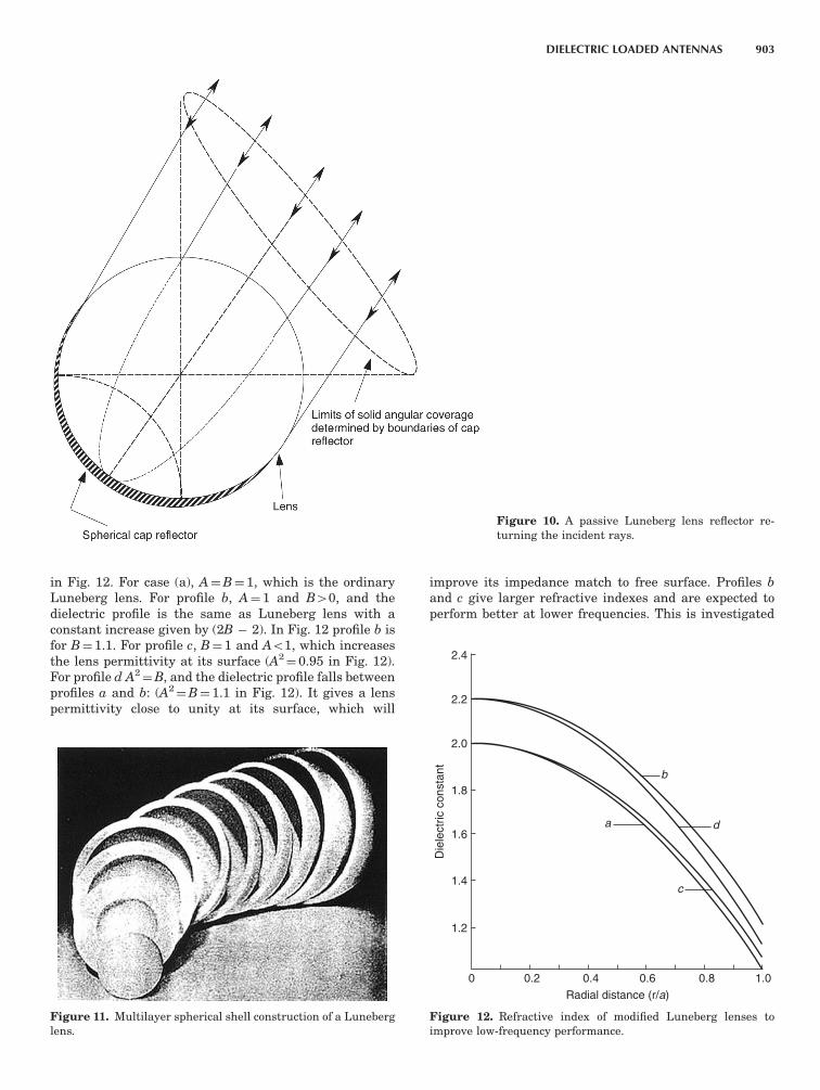
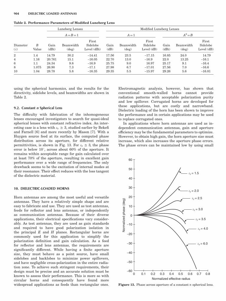
ray paths of this lens are shown in Fig. 9, with a feedhorn on its surface. Scanning the feed on its surfacescans the radiated beam, without alteration. The scanlimit is set only by the mechanical limitation of the feedhorn motion. With a spherical conducting cap on its sur-face the lens also acts as a perfect reflector (i.e., a back-scatterer; Fig. 10). The main difficulty with this lens is itsfabrication problems. Multilayer shells are normally usedto synthesize the refractive index inhomogenity. Figure 11shows one case, where 10 layers are used to construct an18-in. diameter lens. While the approximation to a con-tinuously variable refractive index is reasonable, the wavescattering at the layer transitions reduces the lens effi-ciency.
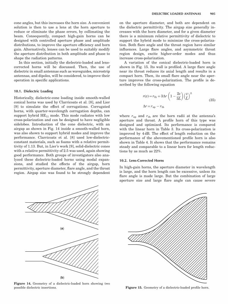
With the abovementioned refractive index, theLuneberg lens performance is ideal at the geometricoptics limits, when the lens diameter in wavelength islarge. At microwave frequencies, the wavelength is largeand the lens diameter in wavelength may not be large.Its performance, namely, directivity, and sidelobe levelsdeteriorate rapidly. In such cases, the refractive indexprofile can be modified to improve its performance. Thiscan be done by determining the excitation efficiencies ofvarious spherical modes and calculating its far field anddirectivity [5]. The new dielectric permittivity profile isdefined as
er¼n2¼ 2B A2 r
a
2ð34Þ
the constant parameters A and B are determined tomaximize the gain. Three different cases are identifiedand investigated. Their refractive index profiles are shown
Feed antenna
Lens
Figure 9. Typical ray paths in a Luneberg lens.
902 DIELECTRIC LOADED ANTENNAS
in Fig. 12. For case (a), A¼B¼1, which is the ordinaryLuneberg lens. For profile b, A¼ 1 and B40, and thedielectric profile is the same as Luneberg lens with aconstant increase given by (2B 2). In Fig. 12 profile b isfor B¼1.1. For profile c, B¼ 1 and Ao1, which increasesthe lens permittivity at its surface (A2
¼ 0.95 in Fig. 12).For profile d A2
¼B, and the dielectric profile falls betweenprofiles a and b: (A2
¼B¼ 1.1 in Fig. 12). It gives a lenspermittivity close to unity at its surface, which will
improve its impedance match to free surface. Profiles band c give larger refractive indexes and are expected toperform better at lower frequencies. This is investigated
Figure 10. A passive Luneberg lens reflector re-turning the incident rays.
Figure 11. Multilayer spherical shell construction of a Luneberglens.
2.4
2.2
2.0
1.8
Die
lect
ric c
onst
ant
1.6
1.4
1.2
0 0.2 0.4
Radial distance (r/a)
0.6 0.8 1.0
b
da
c
Figure 12. Refractive index of modified Luneberg lenses toimprove low-frequency performance.
DIELECTRIC LOADED ANTENNAS 903
using the spherical harmonics, and the results for thedirectivity, sidelobe levels, and beamwidths are shown inTable 2.
9.2. Constant n Spherical Lens
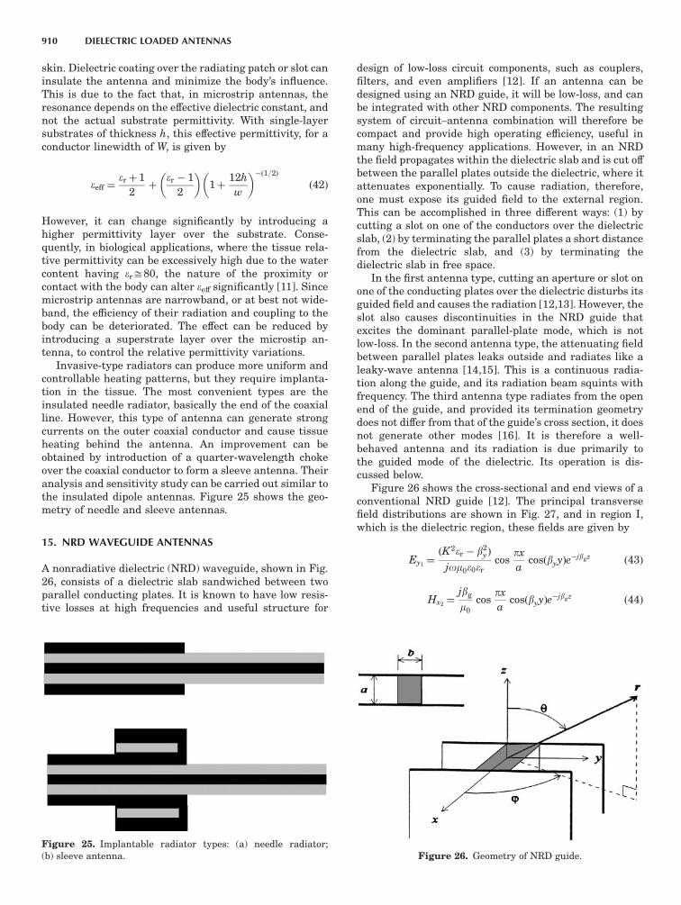
The difficulty with fabrication of the inhomogeneouslenses encouraged investigators to search for quasi-idealspherical lenses with constant refractive index. An inter-esting case is a lens with er ffi 3, studied earlier by Bekefiand Farnell [6] and more recently by Mason [7]. With aHuygen source feed at its surface, the computed phasedistribution across its aperture, for different relativepermittivities, is shown in Fig. 13. For er ffi 3, the phaseerror is below 101, across about 60% of the aperture. Itremains within acceptable range for gain calculated overat least 70% of the aperture, resulting in excellent gainperformance over a wide range of frequencies. The onlydrawback seems to be the excitation of internal modes attheir resonance. Their effect reduces with the loss tangentof the dielectric material.
10. DIELECTRIC-LOADED HORNS
Horn antennas are among the most useful and versatileantennas. They have a relatively simple shape and areeasy to fabricate and use. They are used as test antennas,feeds for reflector and lens antennas, or independentlyas communication antennas. Because of their diverseapplications, their electrical specifications vary consider-ably. As test antennas, they are used as gain standardsand required to have good polarization isolation inthe principal E and H planes. Rectangular horns arecommonly used for this application to simplify thepolarization definition and gain calculation. As a feedfor reflector and lens antennas, the requirements aresignificantly different. While having a finite aperturesize, they must behave as a point source, have smallsidelobes and backlobes to minimize power spillovers,and have negligible cross-polarization in the entire radia-tion zone. To achieve such stringent requirements, theirdesign must be precise and an accurate solution must beknown to assess their performance. This is more so withcircular horns and consequently have found morewidespread applications as feeds than rectangular ones.
Electromagnetic analysis, however, has shown thatconventional smooth-walled horns cannot provideradiation patterns with acceptable polarization purityand low spillover. Corrugated horns are developed forthese applications, but are costly and narrowband.Dielectric loading of the horn has been shown to improvethe performance and in certain applications may be usedto replace corrugated ones.
In applications where horn antennas are used as in-dependent communication antennas, gain and apertureefficiency may be the fundamental parameters to optimize.However, to obtain high gain, the horn aperture size mustincrease, which also increases the aperture phase errors.The phase errors can be maintained low by using small
Table 2. Performance Parameters of Modified Luneberg Lens
Luneberg Lenses Modified Luneberg Lenses
A¼B¼1 A¼1 A2¼B
Diameter(l)
B
ValueGain(dBi)
Beamwidth(deg)
FirstSidelobe
Level (dBi)Gain(dB)
Beamwidth(deg)
FirstSidelobe
Level (dB)Gain(dBi)
Beamwidth(deg)
FirstSidelobe
Level (dB)
2 1.4 14.79 30.2 –14.41 17.56 23.5 –17.15 16.85 24.0 14.794 1.16 20.761 15.1 –16.05 22.70 13.0 –16.9 22.0 13.25 –16.16 1.1 24.34 9.8 –16.9 25.75 9.0 16.97 25.17 9.1 –16.48 1.075 26.90 7.3 –17.1 27.98 6.7 –17.01 27.56 7.0 –16.610 1.04 28.78 5.8 –16.35 29.35 5.5 –15.97 29.26 5.6 –16.81
0.80.70.60.5
Normalized effective radius
0.40.30.20.10−60
−50
−40
−30
−20
−10
0
Nor
mal
ized
pha
se (
deg)
10
20
30
40
50
60
r = 1.5
r = 2.0
r = 2.5
r = 3.0
r = 3.5
r = 4.0
r = 6.0
Figure 13. Phase across aperture of a constant n spherical lens.
904 DIELECTRIC LOADED ANTENNAS
cone angles, but this increases the horn size. A convenientsolution is then to use a lens at the horn aperture toreduce or eliminate the phase errors, by collimating thebeam. Consequently, compact high-gain horns can bedesigned with controlled aperture phase and amplitudedistributions, to improve the aperture efficiency and horngain. Alternatively, lenses can be used to suitably modifythe aperture distribution in both amplitude and phase toshape the radiation patterns.
In this section, initially the dielectric-loaded and lens-corrected horns will be discussed. Then, the use ofdielectric in small antennas such as waveguides, microstripantennas, and dipoles, will be considered, to improve theiroperation in specific applications.
10.1. Dielectric Loading
Historically, dielectric-cone loading inside smooth-walledconical horns was used by Clarricoats et al. [8], and Lier[9] to simulate the effect of corrugations. Corrugatedhorns, with quarter-wavelength corrugation depths, cansupport hybrid HE11 mode. This mode radiates with lowcross-polarization and can be designed to have negligiblesidelobes. Introduction of the cone dielectric, with anairgap as shown in Fig. 14 inside a smooth-walled horn,was also shown to support hybrid modes and improve theperformance. Clarricoats et al. [8] used low-dielectric-constant materials, such as foams with a relative permit-tivity of 1.13. But, in Lier’s work [9], solid-dielectric coneswith a relative permittivity of 2.5 was used, again showinggood performance. Both groups of investigators also ana-lyzed these dielectric-loaded horns using modal expan-sions, and studied the effects of the airgap, hornpermittivity, aperture diameter, flare angle, and the throatregion. Airgap size was found to be strongly dependent
on the aperture diameter, and both are dependent onthe dielectric permittivity. The airgap size generally in-creases with the horn diameter, and for a given diameterthere is a minimum relative permittivity of dielectric tosupport the hybrid mode to minimize the cross-polariza-tion. Both flare angle and the throat region have similarinfluences. Large flare angles, and asymmetric throatregion design, excite higher-order modes and thusincrease cross-polarization.
A variation of the conical dielectric-loaded horn isshown in Fig. 15. Its wall is profiled. A large flare anglenear its throat reduces its axial length and results in acompact horn. Then, its small flare angle near the aper-ture improves the cross-polarization. The profile is de-scribed by the following equation
rðzÞ¼ rthþ 3Dr 12z
3L
z
L
2
Dr¼ rap rth
ð35Þ
where rap and rth are the horn radii at the antenna’saperture and throat. A profile horn of this type wasdesigned and optimized. Its performance is comparedwith the linear horn in Table 3. Its cross-polarization isimproved by 4 dB. The effect of length reduction on theperformance of the abovementioned profile horn is alsoshown in Table 4. It shows that the performance remainssteady and comparable to a linear horn for length reduc-tions by as much as 22%.
10.2. Lens-Corrected Horns
In high-gain horns, the aperture diameter in wavelengthis large, and the horn length can be excessive, unless itsflare angle is made large. But the combination of largeaperture size and large flare angle can cause severe
(a)
(b)
Figure 14. Geometry of a dielectric-loaded horn showing twopossible dielectric insertions. Figure 15. Geometry of a dielectric-loaded profile horn.
DIELECTRIC LOADED ANTENNAS 905

aperture phase error. This problem can be remedied byusing a lens at the horn aperture. Figure 16 shows threepossible options. These simple lenses and others, includ-ing zoned lenses, may be used, and would correct the hornaperture phase distributions. But each lens will havedifferent influences on the aperture amplitude distribu-tion. The properties of the first two lenses were investi-gated earlier, and Table 1 showed their effect on theamplitude distribution. Type (a) (in Fig. 16) increasesthe amplitude taper according to Eq. (21) and will reduceboth sidelobes and the aperture efficiency. Type (b) willcompensate for the amplitude taper, and according toEq. (22), the lens permittivity can be used to control theaperture distribution, and thus the horn efficiency and thepattern sidelobes. For type (c), an analytic expression isnot available and a numerical procedure must be used.However, as was indicated earlier with respect to this lens,both surfaces help in collimating the beam, but its secondsurface is similar to type (b) lens and its influence on theaperture distribution will be similar as well. With ahybrid-mode horn, corrugated or dielectric-loaded, theresulting aperture distributions for different lens relativepermittivities are shown in Fig. 17, which shows that for eraround 1.22, the aperture amplitude distribution is nearlyuniform.
11. DIELECTRIC-LOADED WAVEGUIDES
Waveguides have small aperture size and are not asefficient radiators as horns. Part of the energy leaks outand induces current on the outside wall, which radiateslaterally and backward, causing large backlobes. Thewave impedances of waveguide modes are also differentfrom the free-space intrinsic impedance, and strong reflec-tions can occur on the aperture, causing poor input im-pedance match. These problems can be partly overcome by
flaring the waveguide at its aperture. However, similarand even better performance can be obtained by loadingthe waveguide by a short section of a dielectric. The sizeand shape of the dielectric constant provide several para-meters that can be used to shape the radiation patternsand tailor them to the desired specifications. Table 5shows the results for three different end loadings, andthe type of performance variations one could achieve [2].Two other examples are shown in Figs. 18 and 19, withcombinations of dielectric and cavity loadings [2]. InFig. 18, the end geometry is optimized for nearly perfectpattern symmetry, with negligible cross-polarization. Fig-ure 20 shows its copolar and cross-polar radiation pat-terns. In Fig. 19, the combination was again optimized fora heavily shaped radiation pattern, again with negligiblecross-polarization in the forward direction. It is an idealfeed for deep parabolic reflectors with small f/D¼0.25. Itprovides high aperture efficiency of 81% due to its frontpattern null, very low cross-polarization, and extremely
Table 3. Performancea of Dielectric Loaded Linear andProfiled Horns
Parameter Linear Horn Profiled Horn
3 dB beamwidth (deg) 14.8 13.710 dB beamwidth (deg) 26.9 24.8Directivity (dBi) 22.1 22.5Efficiency (%) 61.8 68.1Peak cross polar (dB) 32.2 36.0VSWR 1.04 1.03
aWhere Rth¼ 1.14 cm, rup¼ 27.7 cm, L¼ 30.9 cm, er¼ 1.13, airgap¼1.2 cm.
Table 4. Performance of Profile Horn with LengthReduction
Length (cm)
PeakCross-Polarization
(dB)
3 dBBeamwidth
(deg) Efficiency (%)
30.9 36.0 13.7 68.127.5 36.8 13.8 64.424.0 31.6 14.0 57.115.0 27.6 16.1 32.0
max
max
F
F
(r, z)
T
D
z
r
F T
(a)
(b)
(c)
Figure 16. Three examples of lens types for loading hornaperture.
906 DIELECTRIC LOADED ANTENNAS

low noise temperatures due to small f/D, the focal length :diameter ratio.
12. MICROSTRIP AND DIELECTRIC RESONATORS
Microstrip antennas are discussed in a separate article(see MICROSTRIP ANTENNAS), and usually consist of a con-ducting patch separated from a ground plane by a di-electric substrate. They are low-profile and increasinglypopular antennas for practically any type of application.Their radiation patterns, however, are asymmetric withunequal E- and H-plane patterns. But, with careful opti-mization, the pattern symmetry can be achieved to
minimize cross-polarization. Figure 21 shows a case ofstacked patches with a side choke for equalizing theprincipal-plane pattern, low backradiation, and cross-polarization. Similar performance can also be obtainedusing a dielectric resonator in lieu of a microstrip patch.The dimensions of the dielectric resonator are related tothe wavelength by
d¼1:841l
4np16þ
pd
1:841h
2" #1=2
ð36Þ
The excited mode is the TM110 mode, and produces radia-tion similar to that of a microstrip patch. In Fig. 22, theresonator and the cavity are optimized for symmetricpattern in the principal planes to reduce the cross-polar-ization. They are shown in Fig. 23, with excellent sym-metry. Both the microstrip and resonator antennas can beused as efficient reflectors and lens feeds with highaperture efficiency and low cross-polarization.
13. INSULATED ANTENNAS
Practically all antennas have conducting parts, but incertain families of antennas, especially small resonant
18
12
6
0
dB
−6
−14
1.1
1.2
1.23
1.5
3020
Horn alone
, deg10
Figure 17. Aperture amplitude distribution for a lens correctedhorn 301 semiflare angle hybrid-mode horn, type c lens.
Figure 18. Geometry of a dielectric cavity-loaded waveguidefeed.
Table 5. Performance of Dielectric-Loaded Waveguide with Shaped Dielectrics
Half-Beamwidths
3 dB 10 dB
GeometryPeak Cross-Polarization
0y90 (dB) Gain (dBi) E plane H plane E plane H plane
a
60°
0.519 33.95 8.28 36.82 36.18 71.47 72.51
b0.1
60°
0.6 24.74 8.11 37.21 38.32 73.42 71.35
c 0.6
0.619
24.43 13.47 19.43 20.25 33.13 35.17
d¼0.6l, er¼2.5
DIELECTRIC LOADED ANTENNAS 907

ones, the conduction current radiates directly. Typicalexamples are the wire antennas and microstrip antennasthat are often half-wavelength resonators. In wire anten-nas, the current is excited by the applied voltage directlyon the wire, which radiates in the surrounding space. Inmicrostrip antennas, the currents are both on the patchand its ground plane, which are separated by a dielectricsubstrate. For this reason, only the patch current is
exposed to the surrounding medium. However, in eithercase, the physical constants of the medium are excessivelylossy, and can short-circuit the antenna current andprevent its operation. In practice, this problem can occurin remote sensing and biological applications. In theformer case, the antennas may be buried underground,or submerged in sea and ocean waters that have highelectrical conductivities. In the latter case, the antennasare implanted into various types of body tissues that canhave excessively high conductivities. In such cases, toensure antenna operation, the conduction currents mustbe insulated from the surrounding conducting medium. Asimple but effective method is to use a thin dielectriccoating on the antenna conductor carrying the radiatingcurrents. The coating will provide insulation between the
0
Rel
ativ
e po
wer
one
way
, dB
−8
−16
−24
−32
−40−180 −135 −90 −45 0
, deg45 90 135 180
Figure 21. Geometry and radiation patterns of a stacked micro-strip feed, with peripheral choke to minimize back radiation.
0
−8
−16
−24
−32
−40
Rel
ativ
e po
wer
one
way
, dB
0 36 72 108 144 180, deg
XZ
Figure 19. Geometry and radiation pattern of a shaped dielectricand cavity loaded waveguide feed.
0
0 60 120 180
−10
Rel
ativ
e po
wer
(dB
)
−20
−30
−40
°
E-planeH-plane
cross-p.
Figure 20. Radiation patterns of the waveguide feed of Fig. 18,showing perfect pattern symmetry and near negligible cross-polarization.
Z
d
h
D
H
3t
Figure 22. Geometry of a dielectric resonator antenna, showinga conducting cavity of height H and diameter D, with a dielectricdisk of height h and diameter d.
908 DIELECTRIC LOADED ANTENNAS

conducting antenna and the medium, thereby eliminatingthe conduction current. The excitation energy will thentransfer into the pointing vector, leaving the antenna.
The behavior of the insulated antennas in a medium ofcomplex permittivity differs considerably from that in freespace, and should be analyzed carefully. For instance,consider a conventional dipole of length 2h, as shown inFig. 24. The wire is a good conductor and has a diameter of
2a, insulated by a cylindrical dielectric region of diameter2b and propagation constant k1, located in an infiniteexterior region of k2. With a thin-wire approximation,the dipole current can be represented by a sinusoidaldistribution of the form described in Ref. 10. The timefactor is assumed to be exp(jot)
IðzÞ¼jV sin kLðh jzjÞ
2Zca cos kLhð37Þ
where
kL¼k1 1þHð2Þ0 ðk2bÞ
k2bHð2Þ1 ðk2bÞ lnb
a
2
6
4
3
7
5
1=2
ð38Þ
Zca¼B1kL
2pk1ln
b
a
ð39Þ
B1¼om0
k1ð40Þ
k1¼o½m1e11=2 ð41Þ
and H0(2) and H1
(2) are Hankel functions of zero and firstorder. Note that with a perfect insulation dielectric k1 isreal but k2 is complex due to the presence of Hankelfunctions in Eq. (38). It reduces to k1 when b, the radiusof the insulation, becomes infinitely large. In view ofEq. (38), the dipole current distribution, input impedance,as well as the radiation resistance, and the resonancefrequency can depend strongly on the radius b andpropagation constant k1, and k2, the propagation constantof the exterior region. The latter may not be fully known,or constant, during the application because of variationsin moisture content and other variables. Thus, the insula-tion parameters should be selected appropriately to mini-mize the dependence of kl on k2.
14. MEDICAL AND BIOLOGICAL ANTENNAS
Another area in which insulated antennas play an im-portant role is the biological and medical applications.They can be noninvasive (i.e., not penetrating the body) orinvasive. In either case, the properties of insulated anten-nas can be significantly different from those in free space.Thus, care must be taken in their design and analysis toensure adequate power transfer to the right tissue. Non-invasive radiators are often dielectric-loaded waveguidesand horns, discussed in the previous section. The dielec-tric loading in this case is used to improve impedancematching and coupling to the body. Their design is notsignificantly different from those of other dielectric-loadedwaveguides, except that the end shaping must preventhotspots and improve penetration.
Microstrip antennas and arrays are other types ofradiators suitable for noninvasive applications. However,their resonance property and power coupling to the bodycan be sensitive to the extent and nature of contact to theFigure 24. Geometry of an insulated dipole antenna.
0
Rel
ativ
e po
wer
(dB
) −10
−20
−30
−40−180 −90 0
°90 180
E-planeH-planecross-p.
Figure 23. Radiation patterns of the dielectric resonator an-tenna.
DIELECTRIC LOADED ANTENNAS 909
skin. Dielectric coating over the radiating patch or slot caninsulate the antenna and minimize the body’s influence.This is due to the fact that, in microstrip antennas, theresonance depends on the effective dielectric constant, andnot the actual substrate permittivity. With single-layersubstrates of thickness h, this effective permittivity, for aconductor linewidth of W, is given by
eeff ¼erþ 1
2þ
er 1
2
1þ12h
w
ð1=2Þ
ð42Þ
However, it can change significantly by introducing ahigher permittivity layer over the substrate. Conse-quently, in biological applications, where the tissue rela-tive permittivity can be excessively high due to the watercontent having erD80, the nature of the proximity orcontact with the body can alter eeff significantly [11]. Sincemicrostrip antennas are narrowband, or at best not wide-band, the efficiency of their radiation and coupling to thebody can be deteriorated. The effect can be reduced byintroducing a superstrate layer over the microstip an-tenna, to control the relative permittivity variations.
Invasive-type radiators can produce more uniform andcontrollable heating patterns, but they require implanta-tion in the tissue. The most convenient types are theinsulated needle radiator, basically the end of the coaxialline. However, this type of antenna can generate strongcurrents on the outer coaxial conductor and cause tissueheating behind the antenna. An improvement can beobtained by introduction of a quarter-wavelength chokeover the coaxial conductor to form a sleeve antenna. Theiranalysis and sensitivity study can be carried out similar tothe insulated dipole antennas. Figure 25 shows the geo-metry of needle and sleeve antennas.
15. NRD WAVEGUIDE ANTENNAS
A nonradiative dielectric (NRD) waveguide, shown in Fig.26, consists of a dielectric slab sandwiched between twoparallel conducting plates. It is known to have low resis-tive losses at high frequencies and useful structure for
design of low-loss circuit components, such as couplers,filters, and even amplifiers [12]. If an antenna can bedesigned using an NRD guide, it will be low-loss, and canbe integrated with other NRD components. The resultingsystem of circuit–antenna combination will therefore becompact and provide high operating efficiency, useful inmany high-frequency applications. However, in an NRDthe field propagates within the dielectric slab and is cut offbetween the parallel plates outside the dielectric, where itattenuates exponentially. To cause radiation, therefore,one must expose its guided field to the external region.This can be accomplished in three different ways: (1) bycutting a slot on one of the conductors over the dielectricslab, (2) by terminating the parallel plates a short distancefrom the dielectric slab, and (3) by terminating thedielectric slab in free space.
In the first antenna type, cutting an aperture or slot onone of the conducting plates over the dielectric disturbs itsguided field and causes the radiation [12,13]. However, theslot also causes discontinuities in the NRD guide thatexcites the dominant parallel-plate mode, which is notlow-loss. In the second antenna type, the attenuating fieldbetween parallel plates leaks outside and radiates like aleaky-wave antenna [14,15]. This is a continuous radia-tion along the guide, and its radiation beam squints withfrequency. The third antenna type radiates from the openend of the guide, and provided its termination geometrydoes not differ from that of the guide’s cross section, it doesnot generate other modes [16]. It is therefore a well-behaved antenna and its radiation is due primarily tothe guided mode of the dielectric. Its operation is dis-cussed below.
Figure 26 shows the cross-sectional and end views of aconventional NRD guide [12]. The principal transversefield distributions are shown in Fig. 27, and in region I,which is the dielectric region, these fields are given by
Ey1¼ðK2er b2
yÞ
jom0e0ercos
px
acosðbyyÞejbgz ð43Þ
Hx2¼
jbg
m0
cospx
acosðbyyÞejbgz ð44Þ
Figure 25. Implantable radiator types: (a) needle radiator;(b) sleeve antenna. Figure 26. Geometry of NRD guide.
910 DIELECTRIC LOADED ANTENNAS
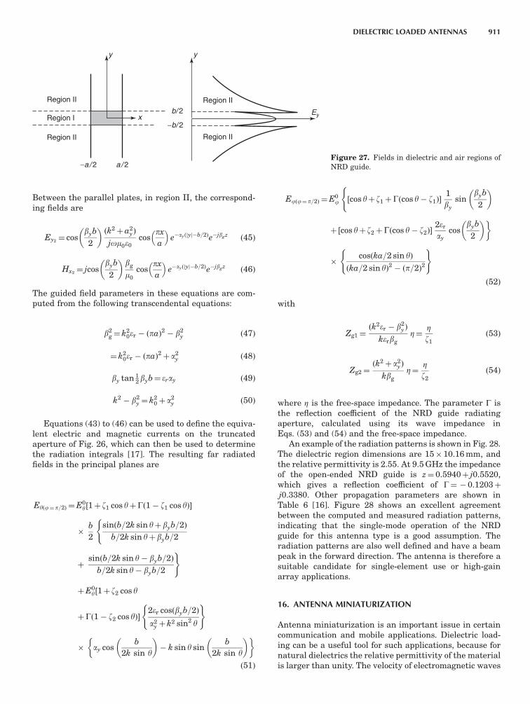
Between the parallel plates, in region II, the correspond-ing fields are
Ey2 ¼ cosbyb
2
ðk2þa2yÞ
jom0e0cos
px
a
eayðjyjb=2Þejbgz ð45Þ
Hx2 ¼ jcosbyb
2
bg
m0
cospx
a
eayðjyjb=2Þejbgz ð46Þ
The guided field parameters in these equations are com-puted from the following transcendental equations:
b2g¼ k2
0er ðpaÞ2 b2y ð47Þ
¼ k20er ðpaÞ2þ a2
y ð48Þ
by tan 12 byb¼ eray ð49Þ
k2 b2y ¼ k2
0þ a2y ð50Þ
Equations (43) to (46) can be used to define the equiva-lent electric and magnetic currents on the truncatedaperture of Fig. 26, which can then be used to determinethe radiation integrals [17]. The resulting far radiatedfields in the principal planes are
Eyðj¼p=2Þ ¼E0y ½1þ z1 cos yþGð1 z1 cos yÞ
b
2
sinðb=2k sin yþ byb=2Þ
b=2k sin yþ byb=2
(
þsinðb=2k sin y byb=2Þ
b=2k sin y byb=2
)
þE0y 1þ z2 cos y½
þGð1 z2 cos yÞ2er cosðbyb=2Þ
a2y þ k2 sin2 y
( )
ay cosb
2k sin y
k sin y sinb
2k sin y
ð51Þ
Ejðj¼ p=2Þ ¼E0j ½cos yþ z1þGðcos y z1Þ
1
by
sinbyb
2
(
þ ½cos yþ z2þGðcos y z2Þ2er
aycos
byb
2
cosðka=2 sin yÞ
ðka=2 sin yÞ2 ðp=2Þ2
( )
ð52Þ
with
Zg1¼ðk2er b2
yÞ
kerbg
Z¼Zz1
ð53Þ
Zg2¼ðk2þ a2
yÞ
kbg
Z¼Zz2
ð54Þ
where Z is the free-space impedance. The parameter G isthe reflection coefficient of the NRD guide radiatingaperture, calculated using its wave impedance inEqs. (53) and (54) and the free-space impedance.
An example of the radiation patterns is shown in Fig. 28.The dielectric region dimensions are 15 10.16 mm, andthe relative permittivity is 2.55. At 9.5 GHz the impedanceof the open-ended NRD guide is z¼ 0.5940þ j0.5520,which gives a reflection coefficient of G¼ 0.1203þj0.3380. Other propagation parameters are shown inTable 6 [16]. Figure 28 shows an excellent agreementbetween the computed and measured radiation patterns,indicating that the single-mode operation of the NRDguide for this antenna type is a good assumption. Theradiation patterns are also well defined and have a beampeak in the forward direction. The antenna is therefore asuitable candidate for single-element use or high-gainarray applications.
16. ANTENNA MINIATURIZATION
Antenna miniaturization is an important issue in certaincommunication and mobile applications. Dielectric load-ing can be a useful tool for such applications, because fornatural dielectrics the relative permittivity of the materialis larger than unity. The velocity of electromagnetic waves
Region IIRegion II
Region I
Region II Region II
Ey
yy
b/ 2
a/ 2−a/ 2
−b/ 2x
Figure 27. Fields in dielectric and air regions ofNRD guide.
DIELECTRIC LOADED ANTENNAS 911
and their wavelengths within the dielectric medium,therefore, reduce by the square root of the relative per-mittivity. Since the waveguide and antenna dimensionsare in terms of the wavelengths, they also become smallerinside dielectrics. Thus, the phenomenon can be usedeffectively for reducing the dimensions of the antennas.In certain applications, such as microstrip antennas, thisis common knowledge, and for the case of dielectricresonators, it was discussed in Section 12. For otherapplications the case must be handled accordingly. Animportant issue is realization of the fact that the normalwavelength reduction by the square root of the relativepermittivity occurs only inside infinite dielectric regions.In other cases, the effect is less and consequently aneffective dielectric constant eeff is normally defined. Formicrostrip substrates this has been determined analyti-cally, and was provided in Eq. (42). In most cases, however,the problem must be solved numerically. Here the case of adielectric-coated monopole is discussed. Monopoles have asimple geometry and are important antenna candidates,but must be installed vertically, making them a tallstructure. A reduction of their length can be very desirablein many applications.
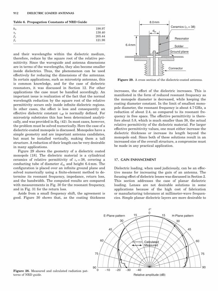
Figure 29 shows the geometry of a dielectric coatedmonopole [18]. The dielectric material is a cylindricalceramics of relative permittivity of er¼ 38, covering aconducting tube of diameter din and height 6.4 mm. Theconfiguration is placed over an infinite ground plane andsolved numerically using a finite-element method to de-termine its resonant frequency, impedance, return loss,and the bandwidth. The computed results are comparedwith measurements in Fig. 30 for the resonant frequency,and in Fig. 31 for the return loss.
Aside from a small frequency shift, the agreement isgood. Figure 30 shows that, as the coating thickness
increases, the effect of the dielectric increases. This ismanifested in the form of reduced resonant frequency asthe monopole diameter is decreased, while keeping thecoating diameter constant. In the limit of smallest mono-pole diameter, the resonant frequency is about 4.7 GHz, areduction of about 2.4, as compared to its resonant fre-quency in free space. The effective permittivity is there-fore about 5.8, which is much smaller than 38, the actualrelative permittivity of the dielectric material. For largereffective permittivity values, one must either increase thedielectric thickness or increase its length beyond themonopole end. Since both of these solutions result in anincreased size of the overall structure, a compromise mustbe made in any practical application.
17. GAIN ENHANCEMENT
Dielectric loading, when used judiciously, can be an effec-tive means for increasing the gain of an antenna. Thefocusing effect of dielectric lenses was discussed in Section 2.This section addresses the case of planar dielectricloading. Lenses are not desirable solutions in someapplications because of the high cost of fabricationor manufacturing tolerances at millimeter-wave frequen-cies. Simple planar dielectric layers are more desirable to
90
75
60
45
30
150°
15
30
45
60
75
900 −10 −20 −30 −40
Relative amplitude (dB)
CalculatedMeasured
E-Plane pattern H-Plane pattern
Figure 28. Measured and calculated radiation pat-terns of NRD guide.
Table 6. Propagation Constants of NRD Guide
k0 198.97ay 138.40by 205.44bz 121.98
8.0mm
6.4mm
din
Ceramics (r = 38)
Resonator
Solder
Ground plane
Connector
Figure 29. A cross section of the dielectric-coated antenna.
912 DIELECTRIC LOADED ANTENNAS

use. They are natural in microstrip structures and cost-effective forms in most radome applications. When usedproperly, they can increase the antenna gain in proportionto their relative permittivity, compared to adjacentregions.
Figure 32 shows the geometry of a typical dielectriccovered region. A planar dielectric layer of thickness t inregion II is placed over another layer of thickness H inregion I, which is over a conducting ground plane. Insideregion I an antenna element is represented by an electriccurrent I0, parallel to the ground plane and at a distanceh. This problem was investigated by Jackson and
7
6
5
41 2 3
din (mm)4 5
Res
onan
t fre
quen
cy (
GH
z)
MeasuredCalculated
Figure 30. Comparison of the calculated and measured resonantfrequencies of antenna in Fig. 29.
Measured
Calculated
0
5
10
Ret
urn
loss
(dB
)
15
204.5 5.0
Frequency (GHz)
5.5
Figure 31. Return loss of the dielectric-coated monopole antenna(din¼3.2 mm) plotted against frequency.
Antenna ground plane
h
t
H
n1 =
n2 =
z
Io
x
Region II
Region I
∈1
∈1
∈2
∈2
Figure 32. Antenna embedded in a two-layerplanar dielectrics.
∈r t
H
D
microstrip
patch
microstrippatch
dielectricradome
cavity
Figure 33. Geometry of a radome-covered cavity antenna.
DIELECTRIC LOADED ANTENNAS 913
Alexopoulos [18] using a transmission-line approximation.They have shown that the optimum thicknesses formaximizing the gain are given by
n1H
l0¼
m
2; m¼ 1; 2; 3; . . . ð55Þ
n2t
l0¼
2n 1
4; n¼1; 2; . . . ð56Þ
n1h
l0¼
2p 1
4; p¼1; 2; . . . ð57Þ
and for this optimum thickness relationships the gain isapproximately
Gain¼ 8H
l0
e2
e1
ð58Þ
This indicates that, if region I is an air medium, thenthe antenna gain increases proportionally to the relative
permittivity of region II. For example, if the relativepermittivity of region II is selected to be 100, then theantenna gain will increase by about 20 dB, over its gainwithout the presence of the dielectric layer. However, thisgain increase is at the expense of the antenna gainbandwidth, which decreases inversely in terms of therelative permittivity.
The antenna spacing of Eq. (57) is not a hard rule andcan be relaxed without a significant gain degradation.This allows the use of the other two parameters inEqs. (55) and (56) to design radomes for gain enhancements.In an earlier study [19], the author placed a microstripantenna at the bottom of a cavity that had a diameterD¼ 2l. A radome was used to cover the cavity. FromEqs. (55) and (56) the optimum radome thickness is aquarter of a dielectric wavelength, and the optimumcavity height must be half-wavelengths. Figure 33 showsthe antenna geometry, and Figs. 34 and 35 provide thevariation of its gain with the cavity and radome thick-nesses. The microstrip antenna gain without the radomewas about 6 dBi, and the computed peak gains, in Figs. 34
Figure 34. Variation of the cavity gain with itsheight H, D¼2.0l,
ffiffiffiffi
erp
t¼0:25; er¼10.
Figure 35. Dependence of the cavity gain onradome thickness, D¼2.0l, H¼0.55l, er¼10.
914 DIELECTRIC LOADED ANTENNAS

and 35, are about 15.7 dBi, indicating an increase of about9.7 dB, which is in good agreement with the prediction ofEq. (58). A set of measured gain patterns, in the principalE and H planes, are shown in Fig. 36. They confirm thepredicted gain enhancement.
BIBLIOGRAPHY
1. S. Silver, Microwave Antenna Theory and Design, PeterPereginus, London, 1984.
2. A. D. Oliver, P. J. B. Clarricoats, A. Kishk, and L. Shafai,Microwave Horns and Feeds, Peter Pereginus, London, 1994.
3. Y. T. Lo and S. W. Lee, Antenna Handbook, Theory Applica-
tions and Design, Van Nostrand Reinhold, New York, 1988,Chapter 16.
4. R. C. Johnson and H. Jasik, Antenna Engineering Handbook,2nd ed., McGraw-Hill, New York, 1984.
5. M. Barakat and L. Shafai, Studies on certain modified Lune-berg lenses, IEE Proc. 130 (Part H)(5):363–368 (Aug. 1983).
6. G. Bekefi and G. W. Farnell, A homogeneous dielectric sphereas a microwave lens, Can. J. Phys. 34:790–803 (1956).
7. V. B. Mason, The Electromagnetic Radiation from SimpleSources in the Presence of a Homogeneous Dielectric Sphere,Ph.D. dissertation, Univ. Michigan, 1972.
8. P. J .B. Clarricoats, A. D. Oliver, and M. Rizk, A dielectricloaded conical feed with low cross-polar radiation, Proc. URSISymp. EM Theory, Spain, Aug. 1983, pp. 351–354.
9. E. Lier, A dielectric hybrid mode antenna feed, a simplealternative to the corrugated horn, IEEE Trans. AP-34:21–29 (1986).
10. R. W. P. King, S. R. Mishra, K. M. Lee, and G. S. Smith, Theinsulated monopole: admittance and junction affect, IEEE
Trans. Anten. Propag. AP-23(2):172–177 (March 1975).
11. I. J. Bahl and S. S. Stuchly, Analysis of a microstrip coveredwith a lossy dielectric, IEEE Trans. Microwave Theory Tech.MTT-28:104–109 (Feb. 1980).
12. J. A. G. Malherbe, The design of a slot array in nonradiatingdielectric waveguide, Part I, theory, IEEE Trans. Anten.Propag. AP-32(12):1335–1340 (Dec. 1984).
13. A. Sanchez and A. A. Oliner, A new leaky waveguide formillimeter waves using nonradiative dielectric (NRD) wave-guide, Part I: Accurate theory, IEEE Trans. Microwave TheoryTech. MTT-35(8):737–747 (Aug. 1987).
14. J. A. G. Malherbe, A leaky-wave antenna in nonradiativedielectric waveguide, IEEE Trans. Anten. Propag. AP-36(9):1231–1235 (Sept. 1988).
15. J. A. G. Malherbe, Radiation from an open-ended nonradia-tive dielectric waveguide, Microwave Opt. Technol. Lett.14(5):266–268 (April 1977).
16. R. E. Colin and F. J. Zucker, Antenna Theory, Part I, McGraw-Hill, New York, 1969.
17. N. Bamba et al., Finite-element analysis of dielectric coatedantenna, Int. Symp. Antennas and Propagation, Sapporo,Japan, Sept. 1992, Vol. 2, pp. 433–436.
18. D. R. Jackson and N. G. Alexopoulos, Gain enhancementmethods for printed circuit antennas, IEEE Trans. Anten.Propag. AP-33(9):976–987 (Sept. 1985).
19. L. Shafai, D. J. Roscoe, and M. Barakat, Simulation andexperimental study of microstrip fed cavity antennas, Int.
Symp. Antennas and Applied Electromagnetics, ANTEM’96,Aug. 1996, pp. 549–554.
Figure 36. Measurement of principal plane patterns of cavity antenna, D¼4 cm, H¼0.9 cm,t¼1.27 mm, er¼10.2, f¼17.2 GHz.
DIELECTRIC LOADED ANTENNAS 915
DIELECTRIC MEASUREMENT
R. BARTNIKAS
IREQ/Institut de Recherched’Hydro-Quebec
Varennes, QuebecCanada
Dielectric measurements are concerned with the charac-terization of solid, liquid, and gaseous insulating materi-als over a wide range of DC and AC conditions at differentfrequencies temperatures, field strengths, and pressures,under differing environments. The frequency range cov-ered extends downward from the power frequency of 50 or60 Hz through the ultralow frequency range from 10 2 to10 6 Hz to DC and upward into the audiofrequency (AF),radiofrequency (RF), and microwave ranges and, finally,into the optical region for optically transparent dielectrics.It can be appreciated that a variety of specimen cells arerequired to suit the nature of the test and to act as con-tainment vessels or holders for the specimens undergoingevaluation. The test methods and specimen containersused over the lower frequency spectrum differ substan-tially from those employed over the higher frequency spec-trum (4300 MHz), because, at lower frequencies, thedielectric specimen behaves as a lumped circuit element,as opposed to its distributed parameter behavior over thehigher frequency region, where the physical dimensions ofthe specimen become of the same order as the wavelengthof the electric field. This delimiting difference necessarilyrequires other test procedures to be utilized at high fre-quencies, and constitutes perhaps the main reason for thebifurcation and the unfortunate, but often attending, iso-lation of the two fields of endeavor—even though the aimover the lower and upper frequency regions is identical,namely, the characterization of dielectric materials.
Space does not permit a detailed description of all thedielectric measurement procedures and, consequently,only a cursory presentation is made. Nor is it possible,within the given constraints, to delve into the various di-electric conduction and loss mechanisms in order to dis-cuss the interpretative aspects of the measurementmethods. Accordingly, the presentation is necessarily con-fined to a concise description of the most common methodsof dielectric measurement employed currently. Whereverfeasible, the methods given attempt to comply with thegeneral guidelines of those specified in national and in-ternational standards, such as those by ASTM (AmericanSociety for Testing and Materials) and IEC (InternationalElectrotechnical Commission), in order to put methodsforward that are universally accepted and have withstoodthe test of time. The dielectric measurement methods pre-sented here will deal principally with those of dc conduc-tivity, dielectric constant and loss as a function offrequency, and voltage breakdown or dielectric strength.
1. DC CONDUCTIVITY MEASUREMENTS
1.1. Volume Resistivity (qv)
Insulating materials employed on electrical equipmentusually characterized by a high insulation resistance
and thus provide an isolating medium between adjacentcomponents that are maintained at different potentials. Incertain applications, such as for capacitor components,bushings, and cables, they must exhibit extremely lowleakage current. In other applications, where partiallyconducting polymers are of interest, the insulation resis-tance values are substantially reduced. Insulation resis-tance measurements, which are generally carried outunder DC conditions, yield not only data on the electricalconduction characteristics of a material, but may also pro-vide an indication of the uniformity or impurity content ofthe insulating material. It is thus of considerable practicalinterest to classify the various insulating materials interms of their DC insulation resistance, which can thenbe related to their DC electrical conductivity. The DC con-ductivity sDC of an insulating or dielectric material, ismore fundamental property, as it bears a direct relation-ship to the conduction mechanisms taking place in thedielectric. It is defined as [1]
sDC¼J‘DC
Eð1Þ
where J‘DC is the DC leakage or conduction current den-sity in A/cm2 and E is the direct electrical field in V/cm; theunits of sDC are S/cm. If it is assumed that the DC con-ductivity arises from a drift of singly charged carriers e inthe field direction, having a charge concentration n percm3 and a mobility of m in cm2 V 1 s 1, then Eq. (1) maybe expressed as
sDC¼ emn ð2Þ
The measured DC volume insulation resistance, Rv, isrelated to the DC volume resistivity of dielectric rv by
rv¼A
dRv ð3Þ
where A is the area of the measuring electrodes in cm2 andd denotes the thickness of the dielectric specimen in cm;by definition, the DC conductivity is inversely related tothe DC volume resistivity as
sDC¼ 1=rv ð4Þ
such that the units of volume resistivity are in O cm.There are various specimen holder electrode systems
and measurement techniques available for determiningthe volume insulation resistance Rv in terms of which thevolume resistivity rv may be computed, employing Eq. (3)[2–4]. For illustrative purposes, only the most prevalentones in use will be considered. Figure 1 depicts a typicalthree-terminal electrode system with the dielectric speci-men held between circular parallel-plane metallic elec-trodes. The electrodes are usually made of stainless steel,with the low-potential (guarded) electrode of diameter D1,having a diameter size less than the high-potential elec-trode, whose diameter D3 is equal to that of the guard ringelectrode. The separation between the latter and the low-potential guarded electrode is equal to g, such that gr2d,
916 DIELECTRIC MEASUREMENT
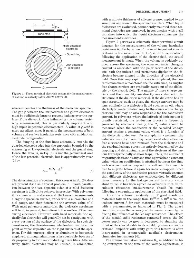
where d denotes the thickness of the dielectric specimen.The gap g between the low-potential and guard electrodesmust be sufficiently large to prevent leakage over the sur-face of the dielectric from influencing the volume resist-ivity measurement; this is particularly important withhigh-input-impedance electrometers. A value of g¼ 2d ismost expedient, since it permits the measurement of bothvolume and surface insulation resistance with an identicalelectrode configuration.
The fringing of the flux lines essentially extends theguarded electrode edge into the gap region bounded by themeasuring or low-potential electrode and the guard ring.Hence the area, A, in Eq. (3) is not the geometrical areaof the low-potential electrode, but is approximately given[2] by
A¼pðD1þ gÞ2
4ð5Þ
The determination of specimen thickness d in Eq. (3), doesnot present itself as a trivial problem [5]. Exact parallel-ism between the two opposite sides of a solid dielectricspecimen is difficult to achieve, in practice. With polymers,it is common to make several thickness measurementsalong the specimen surface, either with a micrometer or adial gauge, and then determine the average value of d.With most polymeric materials, the dielectric specimenswill tend, in general, to conform to the surface of the mea-suring electrodes. However, with hard materials, the op-tically flat electrodes will generally not be contiguous withevery portion of the surface of the dielectric. In such cir-cumstances, the three-terminal electrodes must be eitherpaint or vapor deposited on the rigid surfaces of the spec-imen. For this purpose, silver or aluminum is frequentlyemployed, although aluminum is less desirable, because ofits propensity to form nonconducting oxide films. Alterna-tively, tinfoil electrodes may be utilized, in conjunction
with a minute thickness of silicone grease, applied to en-sure their adhesion to the specimen’s surface. When liquiddielectrics are evaluated, permanently mounted three-ter-minal electrodes are employed, in conjunction with a cellcontainer into which the liquid specimen submerges themeasurement electrodes.
Figure 2 portrays a schematic three-terminal circuitdiagram for the measurement of the volume insulationresistance Rv. Perhaps one of the most important consid-erations in the measurement of Rv is the time at which,following the application of the electric field, the actualmeasurement is made. When the voltage is suddenly ap-plied across the specimen, the observed initial chargingcurrent is associated with the polarization of the dielec-tric; both the induced and permanent dipoles in the di-electric become aligned in the direction of the electricalfield. Once this very rapid process is completed, the cur-rent commences a monotonic decline with time, as surplusfree charge carriers are gradually swept out of the dielec-tric by the electric field. The nature of these charge car-riers and their mobility are directly associated with thestructure of the dielectric material. If the dielectric has anopen structure, such as glass, the charge carriers may beions; similarly, in a dielectric liquid such as an oil, whereelectrolytic contamination may be the source of the chargecarriers, ions may be also responsible for the conductioncurrent. In polymers, where the latitude of ionic motion isgreatly restricted, the conduction process is frequentlygoverned by electrons. Ideally, the Rv value should bemeasured when the conduction or the so-called leakagecurrent attains a constant value, which is a function ofthe dielectric under test. For example, in a polymer, thevalue of constant current may be achieved when all excessfree electrons have been removed from the dielectric andthe residual leakage current is entirely determined by thetrapping and detrapping rates of the electrons at the var-ious traps (principally shallow traps). Thus, the number ofmigrating electrons at any one time approaches a constantvalue when an equilibrium is attained between the timeeach electron resides trapped in a well and the time it isfree to migrate before it again becomes re-trapped. Sincethe complexity of the conduction process virtually ensuresthat different dielectrics are characterized by differenttimes necessary for the leakage current to attain a con-stant value, it has been agreed ad arbitrium that all in-sulation resistance measurements should be madefollowing a one-minute application of the electrical field.
Since the volume resistivity rv of good insulatingmaterials falls in the range from 1012 to 41018O cm, theleakage current Il for such materials must be measuredwith a picoammeter, as indicated in Fig. 2. The guardcircuit improves the accuracy of the measurement by re-ducing the influence of the leakage resistance. The effectsof the coaxial cable resistance connected across the DCpower supply can be greatly decreased by shunting theinput of the coaxial cable to its shield, by means of an op-erational amplifier with unity gain; this feature is oftenincorporated in commercially available electrometer/ohmmeter instruments [6].
The volume insulation resistance Rv, in addition to be-ing contingent on the time of the voltage application, is
D3
D1
D2
Dielectric
High-potentialelectrode
Low-potentialelectrode
Guard ring
g
d
Figure 1. Three-terminal electrode system for the measurementof volume resistivity (after ASTM D257) [3].
DIELECTRIC MEASUREMENT 917
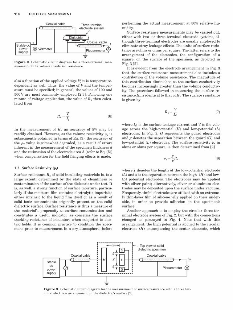
also a function of the applied voltage V; it is temperature-dependent as well. Thus, the value of V and the temper-ature must be specified; in general, the values of 100 and500 V are most commonly employed [2,3]. Following oneminute of voltage application, the value of Rv then calcu-lated from
Rv¼V
Ilð6Þ
In the measurement of Rv an accuracy of 5% may bereadily obtained. However, as the volume resistivity rv issubsequently obtained in terms of Eq. (3), the accuracy ofthe rv value is somewhat degraded, as a result of errorsinherent in the measurement of the specimen thickness dand the estimation of the electrode area A [refer to Eq. (5)]when compensation for the field fringing effects is made.
1.2. Surface Resistivity (qs)
Surface resistance Rs of solid insulating materials is, to alarge extent, determined by the state of cleanliness orcontamination of the surface of the dielectric under test. Itis, as well, a strong function of surface moisture, particu-larly if the moisture film contains electrolytic impuritieseither intrinsic to the liquid film itself or as a result ofsolid ionic contaminants originally present on the soliddielectric surface. Surface resistance is thus a measure ofthe material’s propensity to surface contamination andconstitutes a useful indicator as concerns the surfacetracking resistance of insulators when subjected to elec-tric fields. It is common practice to condition the speci-mens prior to measurement in a dry atmosphere, before
performing the actual measurement at 50% relative hu-midity.
Surface resistance measurements may be carried out,either with two- or three-terminal electrode systems, al-though three-terminal electrodes are usually employed toeliminate stray leakage effects. The units of surface resis-tance are ohms or ohms per square. The latter refers to thearrangement of the electrodes, the configuration of asquare, on the surface of the specimen, as depicted inFig. 3 [2].
It is evident from the electrode arrangement in Fig. 3that the surface resistance measurement also includes acontribution of the volume resistance. The magnitude ofthis contribution diminishes as the surface conductivitybecomes increasingly greater than the volume conductiv-ity. The procedure followed in measuring the surface re-sistance Rs is identical to that of Rv. The surface resistanceis given by
Rs¼V
Islð7Þ
where Isl is the surface leakage current and V is the volt-age across the high-potential (H) and low-potential (L)electrodes. In Fig. 3, G represents the guard electrodesand g denotes the separation between the guard (G) andlow-potential (L) electrodes. The surface resistivity rs inohms or ohms per square, is then determined from [2]
rs¼y
xRs ð8Þ
where y denotes the length of the low-potential electrode(L) and x is the separation between the high- (H) and low-(L) potential electrodes. The electrodes may be appliedwith silver paint; alternatively, silver or aluminum elec-trodes may be deposited upon the surface under vacuum.Frequently, tinfoil electrodes are utilized with an extreme-ly thin-layer film of silicone jelly applied on their under-side, in order to provide adhesion on the specimen’ssurface.
Another approach is to employ the circular three-ter-minal electrode system of Fig. 2, but with the connectionschanged as portrayed in Fig. 4. Note that with thisarrangement, the high potential is applied to the circularelectrode (H) encompassing the center electrode, which
Top view of soliddielectric specimen
V
Coaxial cable Coaxial cableH
x
g
g
yStable
dcpowersupply
G
G
L
Picoammeter A
Isl
Figure 3. Schematic circuit diagram for the measurement of surface resistance with a three ter-minal electrode arrangement on the dielectric’s surface [2].
Dielectric
Picoammeter
Coaxial cableIl
Coaxial cable Three-terminalelectrode system
Stable dcpowersupply
V
+
Voltmeter A
Figure 2. Schematic circuit diagram for a three-terminal mea-surement of the volume insulation resistance.
918 DIELECTRIC MEASUREMENT
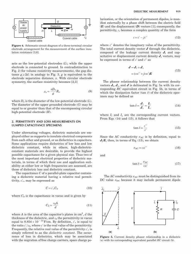
acts as the low-potential electrodes (L), while the upperelectrode is connected to ground. In contradistinction toFig. 2 (for volume resistivity measurements), the gap dis-tance gZ2d; in analogy to Fig. 3, g is equivalent to theelectrode separation distance, x. With circular electrodesymmetry, the surface resistivity becomes [2,3]
rs¼pD1
gRs ð9Þ
where D1 is the diameter of the low-potential electrode (L).The diameter of the upper grounded electrode (G) may beequal to or greater than that of the encompassing circularhigh-potential electrode (H).
2. PERMITTIVITY AND LOSS MEASUREMENTS ONLUMPED CAPACITANCE SPECIMENS
Under alternating voltages, dielectric materials are em-ployed either as supports to insulate electrical componentsfrom each other and ground, or as dielectrics in capacitors.Some applications require dielectrics of low loss and lowdielectric constant, while in others, high-dielectric-constant materials are desirable, to provide the highestpossible capacitance for a given physical size. Thus two ofthe most important electrical properties of dielectric ma-terials, in terms of which their use and application suit-ability at either low or high frequencies are assessed, arethose of dielectric loss and dielectric constant.
The capacitance C of a parallel-plate capacitor contain-ing a dielectric material having a relative real permit-tivity, e0r, may be expressed as
C¼ e0rC0 ð10Þ
where C0 is the capacitance in vacuo and is given by
C0¼e0A
dð11Þ
where A is the area of the capacitor’s plates in cm2, d thethickness of the dielectric, and e0 the permittivity in vacuoequal to 8.8541014 F/cm. By definition, e0r is equal tothe ratio e0=e0, where e0 is the real value of the permittivity.Frequently, the relative real value of the permittivity e0r issimply referred to as the dielectric constant. The occur-rence of loss in dielectrics, which may be associatedwith the migration of free charge carriers, space charge po-
larization, or the orientation of permanent dipoles, is man-ifest externally by a phase shift between the electric field(E) and the displacement (D) vectors [1]; consequently, thepermittivity, e, becomes a complex quantity of the form
e¼ e0 je0 0 ð12Þ
where e00 denotes the imaginary value of the permittivity.The total current density vector J through the dielectric,composed of the leakage current density Jl and cap-acitative or displacement current density Jc vectors, maybe expressed in terms of e0 and e00 as
J¼JlþJc
¼ ðoe0 0 þ joe0ÞEð13Þ
The phasor relationship between the current densityvectors Jl, Jc, and J is delineated in Fig. 5a with its cor-responding RC equivalent circuit in Fig. 5b, in terms ofwhich the dissipation factor (tan d) of the dielectric spec-imen may be defined as
tan d¼Jl
Jc¼
Il
Icð14Þ
where Il and Ic are the corresponding current vectors.From Eqs. (14) and (15), it follows that
tan d¼e0 0
e0ð15Þ
Since the AC conductivity sAC is by definition, equal toJl/E, then, in terms of Eq. (13), we obtain
sAC¼oe0 0 ð16Þ
and
tan d¼sAC
oe0ð17Þ
The AC conductivity sAC must be distinguished from itsDC value sDC because it may include permanent dipole
VH g
Coaxial cableCoaxial cable
L
G
H
Stabledc
powersupply
–
+ADielectric
Isl
Figure 4. Schematic circuit diagram of a three-terminal circularelectrode arrangement for the measurement of the surface insu-lation resistance [3,6].
δ
Jc
Jl
CV
(a) (b)
R
J I
Il IC
Figure 5. Current density phasor relationship in a dielectric(a) with its corresponding equivalent parallel RC circuit (b).
DIELECTRIC MEASUREMENT 919
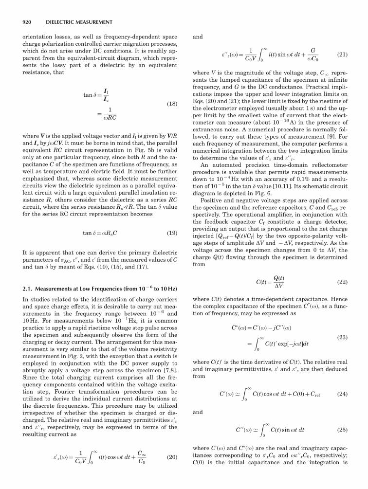
orientation losses, as well as frequency-dependent spacecharge polarization controlled carrier migration processes,which do not arise under DC conditions. It is readily ap-parent from the equivalent-circuit diagram, which repre-sents the lossy part of a dielectric by an equivalentresistance, that
tan d¼Il
Ic
¼1
oRC
ð18Þ
where V is the applied voltage vector and Il is given by V/Rand Ic by joCV. It must be borne in mind that, the parallelequivalent RC circuit representation in Fig. 5b is validonly at one particular frequency, since both R and the ca-pacitance C of the specimen are functions of frequency, aswell as temperature and electric field. It must be furtheremphasized that, whereas some dielectric measurementcircuits view the dielectric specimen as a parallel equiva-lent circuit with a large equivalent parallel insulation re-sistance R, others consider the dielectric as a series RCcircuit, where the series resistance Rs5R. The tan d valuefor the series RC circuit representation becomes
tan d¼oRsC ð19Þ
It is apparent that one can derive the primary dielectricparameters of sAC, e00, and e0 from the measured values of Cand tan d by meant of Eqs. (10), (15), and (17).
2.1. Measurements at Low Frequencies (from 10 6 to 10 Hz)
In studies related to the identification of charge carriersand space charge effects, it is desirable to carry out mea-surements in the frequency range between 10 6 and10 Hz. For measurements below 10 l Hz, it is commonpractice to apply a rapid risetime voltage step pulse acrossthe specimen and subsequently observe the form of thecharging or decay current. The arrangement for this mea-surement is very similar to that of the volume resistivitymeasurement in Fig. 2, with the exception that a switch isemployed in conjunction with the DC power supply toabruptly apply a voltage step across the specimen [7,8].Since the total charging current comprises all the fre-quency components contained within the voltage excita-tion step, Fourier transformation procedures can beutilized to derive the individual current distributions atthe discrete frequencies. This procedure may be utilizedirrespective of whether the specimen is charged or dis-charged. The relative real and imaginary permittivities e0rand e0 0r, respectively, may be expressed in terms of theresulting current as
e0rðoÞ¼1
C0V
Z 1
0
iðtÞ cosot dtþC1C0
ð20Þ
and
e0 0rðoÞ¼1
C0V
Z 1
0iðtÞ sinot dtþ
G
oC0ð21Þ
where V is the magnitude of the voltage step, CN repre-sents the lumped capacitance of the specimen at infinitefrequency, and G is the DC conductance. Practical impli-cations impose the upper and lower integration limits onEqs. (20) and (21); the lower limit is fixed by the risetime ofthe electrometer employed (usually about 1 s) and the up-per limit by the smallest value of current that the elect-rometer can measure (about 10 16 A) in the presence ofextraneous noise. A numerical procedure is normally fol-lowed, to carry out these types of measurement [9]. Foreach frequency of measurement, the computer performs anumerical integration between the two integration limitsto determine the values of e0r and e0 0r.
An automated precision time-domain reflectometerprocedure is available that permits rapid measurementsdown to 104 Hz with an accuracy of 0.1% and a resolu-tion of 105 in the tan d value [10,11]. Its schematic circuitdiagram is depicted in Fig. 6.
Positive and negative voltage steps are applied acrossthe specimen and the reference capacitors, C and Cref, re-spectively. The operational amplifier, in conjunction withthe feedback capacitor Cf constitute a charge detector,providing an output that is proportional to the net chargeinjected [QrefQ(t)/Cf] by the two opposite-polarity volt-age steps of amplitude DV and DV, respectively. As thevoltage across the specimen changes from 0 to DV, thecharge Q(t) flowing through the specimen is determinedfrom
CðtÞ¼QðtÞ
DVð22Þ
where C(t) denotes a time-dependent capacitance. Hencethe complex capacitance of the specimen C*(o), as a func-tion of frequency, may be expressed as
CðoÞ¼C0ðoÞ jC0 0ðoÞ
¼
Z 1
0
CðtÞ0 exp½jotdtð23Þ
where C(t)0 is the time derivative of C(t). The relative realand imaginary permittivities, e0 and e00, are then deducedfrom
C0ðoÞ ’Z 1
0
CðtÞ cosot dtþCð0ÞþCref ð24Þ
and
C0 0ðoÞ ’Z 1
0CðtÞ sinot dt ð25Þ
where C0(o) and C00(o) are the real and imaginary capac-itances corresponding to e0rC0 and oe0 0rC0, respectively;C(0) is the initial capacitance and the integration is
920 DIELECTRIC MEASUREMENT
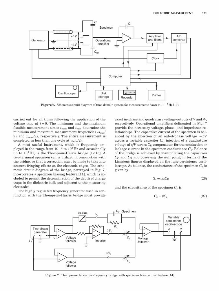
carried out for all times following the application of thevoltage step at t¼ 0. The minimum and the maximumfeasible measurement times tmax and tmin determine theminimum and maximum measurement frequencies omin/2p and omax/2p, respectively. The entire measurement iscompleted in less than one cycle at omin/2p.
A most useful instrument, which is frequently em-ployed in the range from 10 2 to 102 Hz and occasionallyup to 104 Hz, is the Thompson–Harris bridge [12,13]. Atwo-terminal specimen cell is utilized in conjunction withthe bridge, so that a correction must be made to take intoaccount fringing effects at the electrode edges. The sche-matic circuit diagram of the bridge, portrayed in Fig. 7,incorporates a specimen biasing feature [14], which is in-cluded to permit the determination of the depth of chargetraps in the dielectric bulk and adjacent to the measuringelectrodes.
The highly regulated frequency generator used in con-junction with the Thompson–Harris bridge must provide
exact in-phase and quadrature voltage outputs of V and jV,respectively. Operational amplifiers delineated in Fig. 7provide the necessary voltage, phase, and impedance re-lationships. The capacitive current of the specimen is bal-anced by the injection of an out-of-phase voltage bVacross a variable capacitor Cc; injection of a quadraturevoltage of ajV across CR compensates for the conduction orleakage current in the specimen conductance Gx. Balanceof the bridge is achieved by manipulating the capacitorsCC and CR and observing the null point, in terms of theLissajous figures displayed on the long-persistence oscil-loscope. At balance, the conductance of the specimen Gx isgiven by
Gx¼oaCR ð26Þ
and the capacitance of the specimen Cx is
Cx¼bCc ð27Þ
–+
–+
–+
–+
Cx
Rx
Cr
Cc
Two-phasegenerator
Voltagefollower
Voltagefollower
Voltagefollower
dc bias Specimen
Inverter
Variablepersistanceoscilloscope
VVj
x y
α
β
Vs
Vs
Vs
Figure 7. Thompson–Harris low-frequency bridge with specimen bias control feature [14].
–+Generator
Specimen
Operationalamplifier
Amplifierand filters
Diskstorage Recorder
Printer
Clock
Computer
Oscilloscope
A/Dconverter
+∆V
C
Cref
C
–∆V
f
Figure 6. Schematic circuit diagram of time-domain system for measurements down to 104 Hz [10].
DIELECTRIC MEASUREMENT 921

from which the dissipation factor of the dielectric (tan d) isobtained as
tan d¼Gx
oCx
¼aCR
bCc
ð28Þ
Note that a and b are dimensionless quantities, represent-ing the fraction of the voltage, Vs injected across CR andCc, respectively.
Not indicated in Fig. 7 is a zero-offset feature, which isutilized in routine measurements to compensate for theDC coupling circuitry, in order to prevent erratic shifts inthe Lissajous figures while balancing is being carried out.The accuracy of the bridge is 0.1% with resolution ordi-narily better than 0.1%.
Frequency response analyzer methods may also be em-ployed for low-frequency measurements. These computer-ized techniques perform adequately well within the rangefrom 104 to 104 Hz [15].
2.2. Power and Intermediate-Frequency Methods(10 Hz–1 MHz)
A considerable portion of the electrical insulating materi-als manufactured for use in electrical apparatus and ca-bles are evaluated within the frequency range from 50 Hzto 1 MHz, employing primarily bridge type circuits. A fur-ther substantial portion of tests at high voltages are car-ried out at fixed power frequencies of 50, 60, and 400 Hz.The bridge circuits designed for power frequency applica-tions, where measurements are normally made as a func-tion of voltage, differ significantly from those involvingmeasurements as a function of frequency at low voltage.Since most of these tests are performed by means of eitherSchering or transformer ratio arm bridges, the discussionhere will be essentially confined to these types of bridges.
A common low-voltage Schering bridge arrangement,which employs the parallel substitution technique recom-mended in ASTM D150 [16], is depicted in Fig. 8 for thecase where measurements are carried with a two-terminalspecimen cell.
The capacitance C3 is selected such that its negligiblysmall dielectric losses are approximately equal to those ofthe intrinsically low-loss standard capacitor Cs. Note thatthe Schering bridge views the specimen as an equivalentseries RxCx device, so that the variable arm composed ofthe parallel combination of R1 and C1 must be capable ofcompensating for the losses in the small series resistanceRx of the specimen. The null detector, which is normallyan amplifier, is tuned to the frequency of the measure-ment, f¼o/2p. Balance is first obtained by an adjustmentof the capacitors C1 and Cs, with the specimen disconnect-ed. Then, with the specimen placed in parallel with thestandard capacitor Cs, the bridge is rebalanced. The spec-imen capacitance Cx is thus determined from
Cx¼C0s C0 0s ð29Þ
and the dissipation factor from
tan dx¼oR1C0sðC
0 01 C01Þ
ðC0s C0 0sÞð30Þ
where C01;C0s, and C0 01;C0 0s denote the values of the vari-able capacitors C1 and Cs at balance with the specimendisconnected and reconnected, respectively. The substitu-tion technique eliminates the errors introduced by thecoupling effects of the various stray capacitances, but itdoes not circumvent errors arising from connecting leadinfluences.
The procedures for the correction of lead and stray ca-pacitance effects have been standardized and are explicit-ly enumerated in ASTM D150 [16]. It is the inductance, Ls,and the resistance Rs the leads, which contribute to theapparent increase of the capacitance DC and the dissipa-tion factor D tan d in accordance with the relations [16]
DC¼o2LsC2 ð31Þ
and
D tan d¼oRsC ð32Þ
where C is the true capacitance of the specimen; it is to beemphasized that, as the skin effect increases with fre-quency, the lead resistance Rs increases significantly withthe square root of the frequency, f¼o/2p. A standardpractice for assessing the effect of the leads is to performa measurement on a miniature sized capacitor, where thelatter is first directly connected to the bridge terminalsand then inserted across the far end of the leads. The dif-ference between the two readings permits the calculationsof DC and D tan d.
The appearance of an edge capacitance Ce and a groundcapacitance Cg will lead to an increase in the measuredapparent capacitance
Ca¼CþCeþCg ð33Þ
R1 R2
C1
Cs
Cx
Rx
C3
D
Figure 8. Low-voltage Schering bridge, employing the parallelsubstitution technique in accordance with ASTM D150 [16].
922 DIELECTRIC MEASUREMENT

and an apparent dissipation factor
tan da¼C tan d
Cað34Þ
The relative real and imaginary permittivity e0r and e0 0rwill then be given by
e0r¼C
C0
¼Ca ðCeþCgÞ
C0
ð35Þ
and
e0 0r¼Ca tan da=C0 ð36Þ
For the normal type of specimen dimensions, where theparallel-plane cylindrical electrodes are smaller than thediameter of the specimen, the capacitance in vacuo C0
with edge effect correction, may be expressed empiricallyin pF as [16]
C0¼ 0:006954D2
dð37Þ
where d is the thickness of the specimen and D the diam-eter of the electrodes in mm. Exact formulas for the edgecorrection may be found in Ref. 17; the use of the exactformulas does not result in a significant difference for thecorrection. As with all dielectric measurements, the accu-racy attainable is contingent not only upon the accuracy ofthe observed capacitance and tan d values, but also on thestray and edge effects of the electrodes employed, as wellas the calculated interelectrode vacuum capacitance C0. Ingeneral, the permittivity is determinable to within 71%and the tan d value to within 7(5%þ 0.0005) [16].
The circuit of a power frequency high-voltage Scheringbridge, portrayed in Fig. 9, represents essentially an in-verse arrangement of its sibling low-voltage bridge equiv-alent. The lower bridge arms of R4, C4, and R3 constitute
the balancing elements, while the upper arms of the seriesrepresentation of the specimen, R,C, together with thestandard capacitor, Cs, which have a high impedance incomparison with the lower resistive arms, assume themajor portion of the voltage drop. This arrangement pro-vides the bridge with an inherent safety feature, since thelower arms where balance manipulation of the bridge iscarried out, remain at low potential. Figure 9, which rep-resents the classical Schering bridge circuit, delineatesalso the guard circuit’s balancing elements R5 and C5, ar-ranged in accordance with the so-called Wagner’s Earthmethod. The guard circuit, which is implemented in orderto eliminate the stray capacitance to ground, necessarilyentails the use of a three-terminal measurement proce-dure. The solid dielectric slab specimen is placed in athree-terminal cell of the type depicted in Fig. 1, or if thespecimen is a liquid dielectric, a concentric coaxial elec-trode cell [18] may be employed. Frequently, the specimenundergoing test may be a high-voltage power cable or sta-tor bar, whose high-voltage terminated ends must also in-corporate a guard circuit [19]. The standard capacitor Cs,which must be partial-discharge-free up to the maximummeasurement voltage, is normally a 100 pF compressed-gas-filled unit with negligible dielectric loss. Note that thelow-voltage arms are enveloped in grounded shields; theshield, screening the low-potential electrodes of the spec-imen and standard capacitor, including the detector thatnormally comprises an amplifier tuned to the power fre-quency, eliminates the stray capacitances to ground andbetween the components themselves. Thus, any capaci-tance current, which may develop between the detectorand the high-voltage portion of the bridge, flows directly toground via the auxiliary bridge arm of R5 and C5. Sincethe latter are interposed between the shield and thebridge ground, their manipulation balances the guard orshield circuit. The switch SW, shown in Fig. 9, permits thenecessary independent balancing steps for the bridgeguard circuit and the bridge itself. At balance, the capac-itance of the specimen [2] is given by
C¼CsR4
R3ð38Þ
and for equal self-inductances inherent with the resistiveelements R3 and R4, the dissipation factor reduces to
tan d¼oR4C4 ð39Þ
Since high-voltage Schering bridges are normallydesigned to operate at one fixed power frequency, the di-als of R3 and C4 are calibrated to read directly the capac-itance and tan d values of the specimen, respectively. It isto be emphasized that, under high voltage conditions,should the specimen under test undergo partial discharge,then the indicated tan d value will reflect the power lossesdue to partial discharges, in addition to the dielectric loss-es occurring in the solid, liquid, or solid–liquid insulatingsystem of the specimen [20].
R3R5
R4
C5C4
Cs
SW
SpecimenR,C
D
Standardcapacitor,
Figure 9. Classical power frequency circuit of high-voltage Sche-ring bridge with Wagner’s Earth [2].
DIELECTRIC MEASUREMENT 923
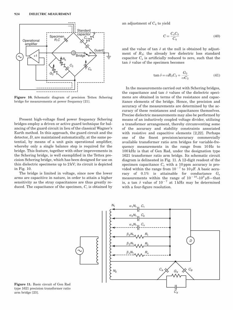
Present high-voltage fixed power frequency Scheringbridges employ a driven or active guard technique for bal-ancing of the guard circuit in lieu of the classical Wagner’sEarth method. In this approach, the guard circuit and thedetector, D, are maintained automatically, at the same po-tential, by means of a unit gain operational amplifier,whereby only a single balance step is required for thebridge. This feature, together with other improvements inthe Schering bridge, is well exemplified in the Tettex pre-cision Schering bridge, which has been designed for use onthin dielectric specimens up to 2 kV; its circuit is depictedin Fig. 10.
The bridge is limited in voltage, since now the lowerarms are capacitive in nature, in order to attain a highersensitivity as the stray capacitances are thus greatly re-duced. The capacitance of the specimen, C, is obtained by
an adjustment of C4 to yield
C¼CsC3
C4ð40Þ
and the value of tan d at the null is obtained by adjust-ment of R3; the already low dielectric loss standardcapacitor Cs is artificially reduced to zero, such that thetan d value of the specimen becomes
tan d¼oR3C3þG3
oC3ð41Þ
In the measurements carried out with Schering bridges,the capacitance and tan d values of the dielectric speci-mens are obtained in terms of the resistance and capac-itance elements of the bridge. Hence, the precision andaccuracy of the measurements are determined by the ac-curacy of these resistances and capacitances themselves.Precise dielectric measurements may also be performed bymeans of an inductively coupled voltage divider, utilizinga transformer arrangement, thereby circumventing someof the accuracy and stability constraints associatedwith resistive and capacitive elements [2,22]. Perhapsone of the finest precision/accuracy commerciallyavailable transformer ratio arm bridges for variable-fre-quency measurements in the range from 10 Hz to100 kHz is that of Gen Rad, under the designation type1621 transformer ratio arm bridge. Its schematic circuitdiagram is delineated in Fig. 11. A 12-digit readout of thespecimen capacitance Cx with a 10 ppm accuracy is pro-vided within the range from 107 to 10 mF. A basic accu-racy of 0.1% is attainable for conductance Gx
measurements within the range of 1010–103 mS—thatis, a tan d value of 10 7 at 1 kHz may be determinedwith a four-figure resolution.
Operationalamplifier
SpecimenR,C
Standardcapacitor
Guard
BridgeR3
G3
C4
C3
Cs
+1D
Figure 10. Schematic diagram of precision Tettex Scheringbridge for measurements at power frequency [21].
N1 C1
C2
Cn
R1
R2
Rn
CA CBGX
CX
N2
D
α
β
1N1
α2N1
2N1
β
β
2N1
α nN1
nN1
Figure 11. Basic circuit of Gen Radtype 1621 precision transformer ratioarm bridge [23].
924 DIELECTRIC MEASUREMENT

The capacitances CA and CB shunting the transformerwinding and the specimen, respectively, do not introduceany error into the measurement, since the former produc-es only a reduction of the voltage across the specimen,while the latter causes only a decrease in the sensitivity ofthe detector D. In balancing the bridge, the multipletapped transformer principle is utilized in the course ofthe resistive and capacitive decade adjustments. Accord-ingly, the balance equation at the null of the bridge isgiven by
N2ðGxþ joCxÞ¼N1½ðb1G1þ b2G2þ þ bnGnÞ
þ joða1C1þ a2C2þ þ anCnÞð42Þ
Equating the real and imaginary terms yields the capac-itance of the specimen
Cx¼N1
N2½a1C1þ a2C2þ þ anCn ð43Þ
and the conductance
Gx¼N1
N2½b1G1þ b2G2þ þ bnGn ð44Þ
The dissipation factor of the specimen as a function offrequency is obtained as
tan d¼Gx
oCx
¼½b1G1þ b2G2þ þ bnGn
o½a1C1þ a2C2þ þ anCn
ð45Þ
Note that the transformer ratio arm bridge views thedielectric specimen as an RC parallel equivalent circuit.
A computer-controlled automatic transformer ratioarm has been developed for measurements at power fre-quencies under high-voltage conditions [24]. The bridgecircuit is delineated schematically in Fig. 12, in which the
Specimen
GroundProtective
ground
Standardcapacitor
Screen 1
Screen 2
ADC Microcomputer
PrinterData and dialog
tanδ
tanδ
range
range
Nulldetector C.T. R
CN1 N2
N2N1
Cx
N4
N3
G1
G2
N4
tanδN3
balance
balance
90° β
α
I1
x,y
Figure 12. Automated power frequency transformer ratio arm bridge with computer control formeasurements at high voltages [24].
DIELECTRIC MEASUREMENT 925
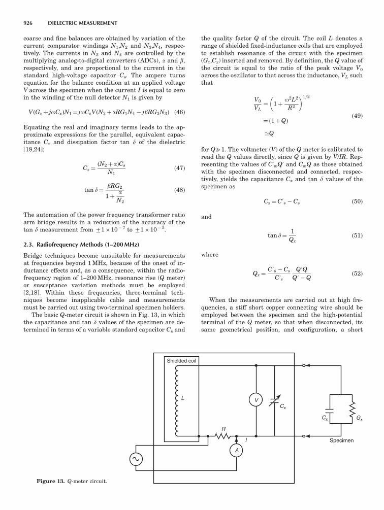
coarse and fine balances are obtained by variation of thecurrent comparator windings N1,N2 and N3,N4, respec-tively. The currents in N3 and N4 are controlled by themultiplying analog-to-digital converters (ADCs), a and b,respectively, and are proportional to the current in thestandard high-voltage capacitor Cs. The ampere turnsequation for the balance condition at an applied voltageV across the specimen when the current I is equal to zeroin the winding of the null detector N1 is given by
VðGxþ joCxÞN1¼ joCsVðN2þ aRG1N4 jbRG2N3Þ ð46Þ
Equating the real and imaginary terms leads to the ap-proximate expressions for the parallel, equivalent capac-itance Cx and dissipation factor tan d of the dielectric[18,24]:
Cx¼ðN2þ aÞCs
N1ð47Þ
tan d¼bRG2
1þa
N2
ð48Þ
The automation of the power frequency transformer ratioarm bridge results in a reduction of the accuracy of thetan d measurement from 7110 7 to 7110 5.
2.3. Radiofrequency Methods (1–200 MHz)
Bridge techniques become unsuitable for measurementsat frequencies beyond 1 MHz, because of the onset of in-ductance effects and, as a consequence, within the radio-frequency region of 1–200 MHz, resonance rise (Q meter)or susceptance variation methods must be employed[2,18]. Within these frequencies, three-terminal tech-niques become inapplicable cable and measurementsmust be carried out using two-terminal specimen holders.
The basic Q-meter circuit is shown in Fig. 13, in whichthe capacitance and tan d values of the specimen are de-termined in terms of a variable standard capacitor Cs and
the quality factor Q of the circuit. The coil L denotes arange of shielded fixed-inductance coils that are employedto establish resonance of the circuit with the specimen(Gx,Cx) inserted and removed. By definition, the Q value ofthe circuit is equal to the ratio of the peak voltage V0
across the oscillator to that across the inductance, VL suchthat
V0
VL¼ 1þ
o2L2
R2
1=2
¼ ð1þQÞ
’Q
ð49Þ
for Qb1. The voltmeter (V) of the Q meter is calibrated toread the Q values directly, since Q is given by V/IR. Rep-resenting the values of C0s,Q
0 and Cs,Q as those obtainedwith the specimen disconnected and connected, respec-tively, yields the capacitance Cx and tan d values of thespecimen as
Cx¼C0s Cs ð50Þ
and
tan d¼1
Qxð51Þ
where
Qx¼C0s Cs
C0s
Q0Q
Q0 Qð52Þ
When the measurements are carried out at high fre-quencies, a stiff short copper connecting wire should beemployed between the specimen and the high-potentialterminal of the Q meter, so that when disconnected, itssame geometrical position, and configuration, a short
Shielded coil
Specimen
Cx
L V
A
R
I
Cx Gx
Figure 13. Q-meter circuit.
926 DIELECTRIC MEASUREMENT
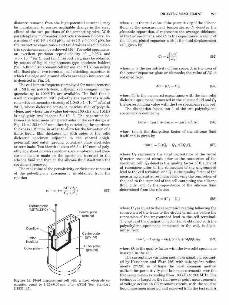
distance removed from the high-potential terminal, maybe maintained, to ensure negligible change in the strayeffects of the two positions of the connecting wire. Withparallel-plane micrometer electrode specimen holders, ac-curacies of 7(0.1%þ 0.02 pF) and 7(2%þ 0.00005 pF), forthe respective capacitance and tan d values of solid dielec-tric specimens may be achieved [16]. For solid specimens,an excellent precision reproducibility of 70.05% and75105 for Cx and tan d, respectively, may be obtainedby means of liquid displacement-type specimen holders[25]. A fluid displacement cell for use at 1 MHz, consistingof a fixed-plate, two-terminal, self-shielding capacitor, inwhich the edge and ground effects are taken into account,is depicted in Fig. 14.
The cell is most frequently employed for measurementsat 1 MHz on polyethylene, although cell designs for fre-quencies up to 100 MHz are available. The fluid that isused in conjunction with polyethylene specimens is sili-cone with a kinematic viscosity of 1.0 cSt (110 6 m2/s) at231C, whose dielectric constant matches that of polyeth-ylene, and whose tan d value between 100 kHz and 1 MHzis negligibly small (about 5 10 5). The separation be-tween the fixed measuring electrodes of the cell design inFig. 14 is 1.5270.05 mm, thereby restricting the specimenthickness 1.27 mm, in order to allow for the formation of afinite liquid film thickness on both sides of the soliddielectric specimen adjacent to the central (high-potential) and outer (ground potential) plate electrodesor terminals. Two identical sizes (68.3 100 mm) of poly-ethylene sheet or slab specimens are employed, and mea-surements are made on the specimens inserted in thesilicone fluid and then on the silicone fluid itself with thespecimens removed.
The real value of the permittivity or dielectric constantof the polyethylene specimen e0 is obtained from therelation
ðe0 e0lÞ¼DC
C0
d0
d
ð53Þ
where e0l is the real value of the permittivity of the siliconefluid at the measurement temperature, d0 denotes theelectrode separation, d represents the average thicknessof the two specimens, and C0 is the capacitance in vacuo ofthe double-plated capacitor within the fluid displacementcell, given by
C0¼ 2e0A
d0
ð54Þ
where e0 is the permittivity of free space, A is the area ofthe center capacitor plate or electrode; the value of DC isobtained from
DC¼ ðC2 C1Þ ð55Þ
where C2 is the measured capacitance with the two soliddielectric specimens immersed in the silicone fluid and C1
the corresponding value with the two specimens removed.The dissipation factor, tan d, of the two polyethylene
specimens is defined by
tan d¼ tan dlþ ðtan dc tan dlÞ½d0=d ð56Þ
where tan dl the dissipation factor of the silicone fluiditself and is given by
tan dl¼CTðQc Q1Þ=ClQ0Q1 ð57Þ
where CT represents the total capacitance of the tunedQ-meter resonant circuit prior to the connection of thespecimen cell, Q0 denotes the quality factor of the circuitat resonance prior to the connection of the ungroundedlead to the cell terminal, and Q1 is the quality factor of themeasuring circuit at resonance following the connection ofthe lead to the terminal of the cell containing the siliconefluid only, and Cl the capacitance of the silicone fluiddetermined from the relation
Cl¼ ðC01 C1Þ ð58Þ
where C01 is equal to the capacitance reading following theconnection of the leads to the circuit terminals before theconnection of the ungrounded lead to the cell terminal.The value of the dissipation factor tan dc obtained with thepolyethylene specimens immersed in the cell, is deter-mined from
tan dc¼CTðQ0 Q2Þ=ðe0lC0þDQÞQ0Q2 ð59Þ
where Q2 is the quality factor with the two solid specimensinserted in the cell.
The susceptance variation method originally propound-ed by Hartshorn and Ward [26] with subsequent refine-ments [27,28] is perhaps the most common methodutilized for permittivity and loss measurements over thefrequency region extending from 100 kHz to 200 MHz. Thetechnique is based on the half-power point measurementsof voltage across an LC resonant circuit, with the solid orliquid specimen inserted and removed from the test cell. A
Central plateterminal
Center plate(ground)
Outer plate(ground)Outer plate
Tefloninsulator
Overflow
Thermometer(ASTM 23°C)
Figure 14. Fluid displacement cell with a fixed electrode se-paration equal to 1.5270.05 mm after ASTM Test StandardD1531 [25].
DIELECTRIC MEASUREMENT 927

modified susceptance variation circuit and a cross-section-al profile view of the associated micrometer adjustableholder for solid specimens are depicted in Figs. 15 and 16,respectively. For liquids, the specimen holder is similar tothat depicted in Fig. 16, except that two parallel concaveelectrodes are employed to permit containment of theliquid specimen.
The micrometer adjustable electrode system depictedin Fig. 16 portrays a solid dielectric specimen betweenplane-parallel electrodes. In the measurement procedure,resonance is first established with the specimen insertedbetween the electrodes and the maximum value of thevoltage e1 of the AC–DC converter is recorded. Thereafter,the specimen is removed and the separation of the elec-trodes is reduced until resonance is reestablished; thisresonance point is characterized by a larger output voltageeo of the AC–DC converter. The capacitance of this air gapspacing is numerically equal to the capacitance of thespecimen Cx and is obtained directly from the calibratedreading of the main micrometer setting. Manipulation ofthe main micrometer head, in conjunction with the smallvernier or incremental capacitor, yields the half-powerpoints of the resonance curve; the resulting width of theresonance curve is equivalent to a capacitance change,designated as DC0. It is the square law detection featureof the instrument that relates the DC0 value directly tothe recorded change of reading in the incremental capac-itor. Hence the dissipation factor of the specimen [27] is
given by
tan d¼e0
e1
1=2
1
" #
DC0
2Cxð60Þ
The real value of the permittivity e0r is normally obtainedin terms of the thickness of the specimen ds and the quan-tity, Dd
e0r¼ds
ds Ddð61Þ
where Dd represents the decrease in separation of themain electrodes in air required to restore the same capac-itance as that obtained with the specimen placed betweenthe electrodes. An accuracy of 1% is achievable on permit-tivity measurements and tan d may be determined towithin 71.0 10 6.
3. PERMITTIVITY AND LOSS MEASUREMENTS ONDISTRIBUTED PARAMETER SPECIMENS
Dielectric specimens behave as distributed parameter sys-tems when the wavelength of the electromagnetic fieldbecomes comparable to or is less than the physical dimen-sions of the specimen. The transition from lumped to dis-tributed parameter behavior occurs generally within thefrequency range from 300 MHz to 600 MHz. The high-fre-quency dielectric measurements represent a vast area ofendeavor, which involves the use of resonant cavities ofcylindrical and rectangular shapes, waveguides, or trans-mission lines, including quasioptical procedures, as wellas optical methods requiring the use of spectrometers andinterferometers. Since it would not be feasible within thespace constrains to cover, even in a cursory manner, alltest method variations over the millimeter and submilli-meter wavelengths, the test procedures followed over thisrange of frequencies will be illustrated by a number ofwidely used and representative test methods.
3.1. Reentrant Cavity Method (300–600 MHz)
The reentrant cavity measurement technique constitutes,in essence, an extension of the Hartshorn–Ward method; ituses the same specimen cell arrangement, with the
Coupling coils
Recorderac–dc
converter
Adjustableelectrodes and
specimen Incrementalcapacitor
Potentiometer
Figure 15. Schematic circuit diagramof modified Hartshorn–Ward suscep-tance variation circuit [27].
Micrometer screw
Bellows
Grounded electrode
Solid specimen
High-potentialelectrode
High-potential electrode
Grounded terminal
Vernier (incremental)capacitor
Figure 16. Micrometer adjustable electrode for use in conjunc-tion with the susceptance variation circuit [26].
928 DIELECTRIC MEASUREMENT
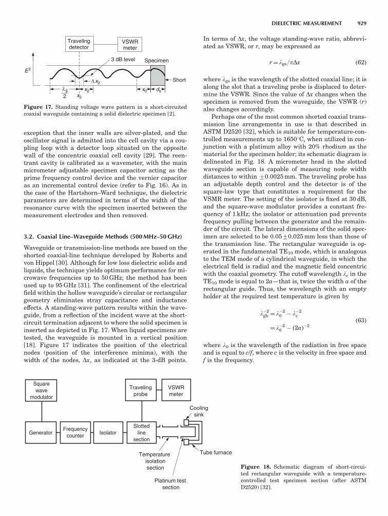
exception that the inner walls are silver-plated, and theoscillator signal is admitted into the cell cavity via a cou-pling loop with a detector loop situated on the oppositewall of the concentric coaxial cell cavity [29]. The reen-trant cavity is calibrated as a wavemeter, with the mainmicrometer adjustable specimen capacitor acting as theprime frequency control device and the vernier capacitoras an incremental control device (refer to Fig. 16). As inthe case of the Hartshorn–Ward technique, the dielectricparameters are determined in terms of the width of theresonance curve with the specimen inserted between themeasurement electrodes and then removed.
3.2. Coaxial Line–Waveguide Methods (500 MHz–50 GHz)
Waveguide or transmission-line methods are based on theshorted coaxial-line technique developed by Roberts andvon Hippel [30]. Although for low loss dielectric solids andliquids, the technique yields optimum performance for mi-crowave frequencies up to 50 GHz; the method has beenused up to 95 GHz [31]. The confinement of the electricalfield within the hollow waveguide’s circular or rectangulargeometry eliminates stray capacitance and inductanceeffects. A standing-wave pattern results within the wave-guide, from a reflection of the incident wave at the short-circuit termination adjacent to where the solid specimen isinserted as depicted in Fig. 17. When liquid specimens aretested, the waveguide is mounted in a vertical position[18]. Figure 17 indicates the position of the electricalnodes (position of the interference minima), with thewidth of the nodes, Dx, as indicated at the 3-dB points.
In terms of Dx, the voltage standing-wave ratio, abbrevi-ated as VSWR, or r, may be expressed as
r¼ lgs=pDx ð62Þ
where lgs is the wavelength of the slotted coaxial line; it isalong the slot that a traveling probe is displaced to deter-mine the VSWR. Since the value of Dx changes when thespecimen is removed from the waveguide, the VSWR (r)also changes accordingly.
Perhaps one of the most common shorted coaxial trans-mission line arrangements in use is that described inASTM D2520 [32], which is suitable for temperature-con-trolled measurements up to 16501C, when utilized in con-junction with a platinum alloy with 20% rhodium as thematerial for the specimen holder; its schematic diagram isdelineated in Fig. 18. A micrometer head in the slottedwaveguide section is capable of measuring node widthdistances to within 70.0025 mm. The traveling probe hasan adjustable depth control and the detector is of thesquare-law type that constitutes a requirement for theVSMR meter. The setting of the isolator is fixed at 30 dB,and the square-wave modulator provides a constant fre-quency of 1 kHz; the isolator or attenuation pad preventsfrequency pulling between the generator and the remain-der of the circuit. The lateral dimensions of the solid spec-imen are selected to be 0.0570.025 mm less than those ofthe transmission line. The rectangular waveguide is op-erated in the fundamental TE10 mode, which is analogousto the TEM mode of a cylindrical waveguide, in which theelectrical field is radial and the magnetic field concentricwith the coaxial geometry. The cutoff wavelength lc in theTE10 mode is equal to 2a—that is, twice the width a of therectangular guide. Thus, the wavelength with an emptyholder at the required test temperature is given by
l2gh ¼ l2
0 l2c
¼ l20 ð2aÞ2
ð63Þ
where l0 is the wavelength of the radiation in free spaceand is equal to c/f, where c is the velocity in free space andf is the frequency.
Travelingdetector
VSWRmeter
Specimen
Short
E2
x0 dsx2x2
x2
λg
2
3 dB level
∆
Figure 17. Standing voltage wave pattern in a short-circuitedcoaxial waveguide containing a solid dielectric specimen [2].
Squarewave
modulator
Travelingprobe
VSWRmeter
Generator IsolatorFrequency
counter
Slottedline
section
Coolingsink
Temperature isolationsection
Platinum test section
Tube furnace
Figure 18. Schematic diagram of short-circui-ted rectangular waveguide with a temperature-controlled test specimen section (after ASTMD2520) [32].
DIELECTRIC MEASUREMENT 929

With the specimen of thickness ds inserted adjacent tothe short in the waveguide, the impedance of the line atthe specimen–air interface [33] is given by
Zin¼ ðjom0=g2Þ tanhðg2dsÞ ð64Þ
where m0 is the permeability of the nonmagnetic dielectricmaterial, which is identical to that in free space. Assum-ing negligible losses in the walls of the waveguide, thepropagation constant of the coaxial waveguide g2 contain-ing the specimen is given by
g2¼ 2pðl2c e0rl
20 Þ
1=2ð65Þ
The load impedance at a phase distance j from the ob-served electrical node for the value of the VSWR r given byEq. (62), (34) is
Zmeas¼ fm0lg½ð1 jr tanjÞ=ðr j tanjÞ ð66Þ
where lg is the wavelength of the guide and is equal to2p/b2; here b2 is the phase coefficient of the waveguidewith the specimen inserted; j is the corrected phase dis-tance, defined by
j¼ 2p½ðN=2Þ ðds=lghÞ ðx2 x1Þlgs ð67Þ
where N represents the smallest integer for which j ispositive, x2 is the position of the traveling detector withthe specimen inserted, as indicated in Fig. 17, and x1 is theequivalent distance with the specimen removed.
Equating the impedances Zin and Zmeas yields
tanh l2ds
g2
¼lghð1 jr tanjÞ2pjðr j tanjÞ
ð68Þ
Equating the real and imaginary terms yields the rela-tive real value of the permittivity e0r of the specimen as
e0r¼ ½ðb2=2pÞ2þ l2
c =l20 ð69Þ
and, for low-loss specimens [34], the dissipation factorsimplifies to
tan d¼Dxð1 l2
0=e0rl2
c Þð1þ tan2 jÞdsf½1þ tan2 b2ds ½ðtan b2dsÞ=b2dsg
ð70Þ
where the width of the node Dx that would be measured atthe face of the specimen is given by
Dx¼Dx2 Dx1 ð71Þ
The principal factors affecting the accuracy of the mea-surements are associated with the assumption that lossesat the walls of the waveguide are negligible and that thefinite airgap between the solid specimen and the walls ofthe waveguide does not influence appreciably the results;evidently, the latter error does not arise with liquid spec-imens [18]. However, accuracies of 71% for e0r and7200 radians for the loss angle d are achievable.
3.3. Resonant Cavity Methods (about 500 MHz–60 GHz)
A resonating cavity may be viewed as a transmission line,which is shortened at both ends that are separated by anarbitrary multiple of one-half the operating wavelength.The insertion of a dielectric specimen into the cavity altersthe wavelength and, as a consequence, the change in thequality factor Q of the cavity with the specimen insertedand removed can be used to derive the dielectric param-eters of the specimen. Since resonant cavities have intrin-sically high values of Q, they constitute an effective meansfor measuring low-loss dielectric materials. The specimensmay have different geometrical configurations such asspheres, sheets, disks, rods, and so forth, and may fillthe cross section of the beam, if necessary. The requiredspecimen size becomes smaller as the cavity size dimin-ishes with frequency, thereby also necessitating a redesignof the cavity with each octave increase in frequency. Forfrequencies above 60 MHz, the reduced cavity sizes, irre-spective of their shape, rapidly approach a practical limit.Although open resonant cavities or interferometers mayexceed substantially the frequency of 60 MHz [35] theirapplicability is confined to specimens having dielectricconstants in excess of 5.
A coaxial waveguide shorted at one end becomes a res-onant cavity when shorted at both ends. It may be reso-nated either by varying the frequency of the externallyapplied field or by varying the radial or axial dimensionsof the cavity itself. A very widely used rectangular micro-wave cavity design for operation in the transverse electricfield, TE1ON mode, is depicted in Fig. 19. Note that, in themode designation code, the first subscript denotes thenumber of half-waves across the short-circuited wave-guide, the second subscript refers to the number of half-waves from top to bottom of the waveguide, and the thirdsubscript represents the odd number of half-waves alongthe waveguide. The closed cavity arrangement in Fig. 19 isidentical to that given in the test method described inASTM D2520 [32]. It is of paramount importance that thediameter of the iris holes in the transmitting and detect-ing ends be small to achieve high Q values. The particulardesign of the shown resonant cavity is intended for usewith solid rod-shaped specimens, which are held suspend-ed between the top and bottom holes that are drilled intothe waveguide (refer to Fig. 19). The resonant frequency of
Shorting plate
Solid roddielectricspecimen
Electricfield vector
w
h
d
Iris hole(dia. = h/2.2)
Figure 19. Closed rectangular resonant cavity for tests on solidrod-shaped dielectric specimens (after ASTM D2520) [32].
930 DIELECTRIC MEASUREMENT
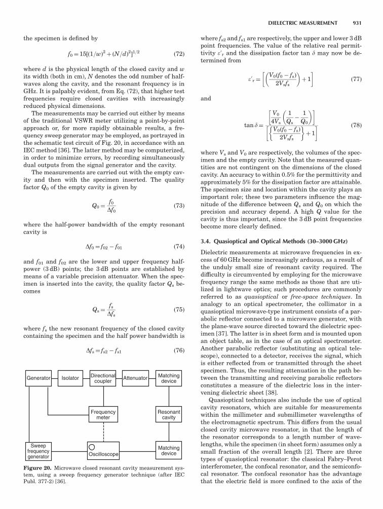
the specimen is defined by
f0¼ 15½ð1=wÞ2þ ðN=dÞ21=2 ð72Þ
where d is the physical length of the closed cavity and wits width (both in cm), N denotes the odd number of half-waves along the cavity, and the resonant frequency is inGHz. It is palpably evident, from Eq. (72), that higher testfrequencies require closed cavities with increasinglyreduced physical dimensions.
The measurements may be carried out either by meansof the traditional VSWR meter utilizing a point-by-pointapproach or, for more rapidly obtainable results, a fre-quency sweep generator may be employed, as portrayed inthe schematic test circuit of Fig. 20, in accordance with anIEC method [36]. The latter method may be computerized,in order to minimize errors, by recording simultaneouslydual outputs from the signal generator and the cavity.
The measurements are carried out with the empty cav-ity and then with the specimen inserted. The qualityfactor Q0 of the empty cavity is given by
Q0¼f0
Df0ð73Þ
where the half-power bandwidth of the empty resonantcavity is
Df0¼ f02 f01 ð74Þ
and f01 and f02 are the lower and upper frequency half-power (3 dB) points; the 3 dB points are established bymeans of a variable precision attenuator. When the spec-imen is inserted into the cavity, the quality factor Qs be-comes
Qs¼fs
Dfsð75Þ
where fs the new resonant frequency of the closed cavitycontaining the specimen and the half power bandwidth is
Dfs¼ fs2 fs1 ð76Þ
where fs2 and fs1 are respectively, the upper and lower 3 dBpoint frequencies. The value of the relative real permit-tivity e0r and the dissipation factor tan d may now be de-termined from
e0r¼V0ðf0 fsÞ
2Vsfs
þ 1
ð77Þ
and
tan d¼
V0
4Vs
1
Qs
1
Q0
V0ðf0 fsÞ
2Vsfs
þ 1
ð78Þ
where Vs and V0 are respectively, the volumes of the spec-imen and the empty cavity. Note that the measured quan-tities are not contingent on the dimensions of the closedcavity. An accuracy to within 0.5% for the permittivity andapproximately 5% for the dissipation factor are attainable.The specimen size and location within the cavity plays animportant role; these two parameters influence the mag-nitude of the difference between Qs and Q0 on which theprecision and accuracy depend. A high Q value for thecavity is thus important, since the 3 dB point frequenciesbecome more clearly defined.
3.4. Quasioptical and Optical Methods (30–3000 GHz)
Dielectric measurements at microwave frequencies in ex-cess of 60 GHz become increasingly arduous, as a result ofthe unduly small size of resonant cavity required. Thedifficulty is circumvented by employing for the microwavefrequency range the same methods as those that are uti-lized in lightwave optics; such procedures are commonlyreferred to as quasioptical or free-space techniques. Inanalogy to an optical spectrometer, the collimator in aquasioptical microwave-type instrument consists of a par-abolic reflector connected to a microwave generator, withthe plane-wave source directed toward the dielectric spec-imen [37]. The latter is in sheet form and is mounted uponan object table, as in the case of an optical spectrometer.Another parabolic reflector (substituting an optical tele-scope), connected to a detector, receives the signal, whichis either reflected from or transmitted through the sheetspecimen. Thus, the resulting attenuation in the path be-tween the transmitting and receiving parabolic reflectorsconstitutes a measure of the dielectric loss in the inter-vening dielectric sheet [38].
Quasioptical techniques also include the use of opticalcavity resonators, which are suitable for measurementswithin the millimeter and submillimeter wavelengths ofthe electromagnetic spectrum. This differs from the usualclosed cavity microwave resonator, in that the length ofthe resonator corresponds to a length number of wave-lengths, while the specimen (in sheet form) assumes only asmall fraction of the overall length [2]. There are threetypes of quasioptical resonator: the classical Fabry–Perotinterferometer, the confocal resonator, and the semiconfo-cal resonator. The confocal resonator has the advantagethat the electric field is more confined to the axis of the
Generator Isolator AttenuatorDirectionalcoupler
Matchingdevice
Matchingdevice
Resonantcavity
Frequencymeter
Sweepfrequencygenerator Oscilloscope
Figure 20. Microwave closed resonant cavity measurement sys-tem, using a sweep frequency generator technique (after IECPubl. 377-2) [36].
DIELECTRIC MEASUREMENT 931
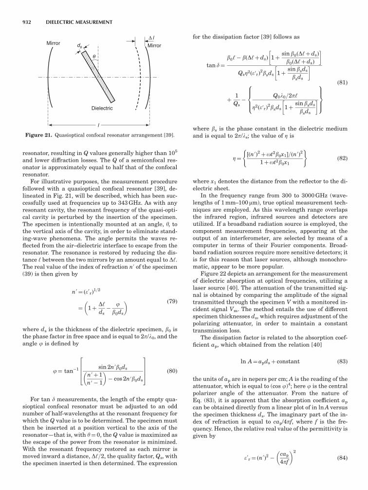
resonator, resulting in Q values generally higher than 105
and lower diffraction losses. The Q of a semiconfocal res-onator is approximately equal to half that of the confocalresonator.
For illustrative purposes, the measurement procedurefollowed with a quasioptical confocal resonator [39], de-lineated in Fig. 21, will be described, which has been suc-cessfully used at frequencies up to 343 GHz. As with anyresonant cavity, the resonant frequency of the quasi-opti-cal cavity is perturbed by the insertion of the specimen.The specimen is intentionally mounted at an angle, y, tothe vertical axis of the cavity, in order to eliminate stand-ing-wave phenomena. The angle permits the waves re-flected from the air–dielectric interface to escape from theresonator. The resonance is restored by reducing the dis-tance ‘ between the two mirrors by an amount equal to D‘.The real value of the index of refraction n0 of the specimen(39) is then given by
n0 ¼ ðe0rÞ1=2
¼ 1þD‘ds
jb0ds
ð79Þ
where ds is the thickness of the dielectric specimen, b0 isthe phase factor in free space and is equal to 2p/l0, and theangle j is defined by
j¼ tan1 sin 2n0b0ds
n0 þ 1
n0 1
cos 2n0b0ds
2
6
6
4
3
7
7
5
ð80Þ
For tan d measurements, the length of the empty qua-sioptical confocal resonator must be adjusted to an oddnumber of half-wavelengths at the resonant frequency forwhich the Q value is to be determined. The specimen mustthen be inserted at a position vertical to the axis of theresonator—that is, with y¼ 0, the Q value is maximized asthe escape of the power from the resonator is minimized.With the resonant frequency restored as each mirror ismoved inward a distance, D‘=2, the quality factor, Qs, withthe specimen inserted is then determined. The expression
for the dissipation factor [39] follows as
tan d¼b0‘ bðD‘þdsÞ 1þ
sin b0ðD‘þdsÞ
b0ðD‘þdsÞ
QsZ2ðe0rÞ2bsds 1þ
sinbsds
bsds
þ1
Qs
Q0l0=2p‘
Z2ðe0rÞ2bsds 1þ
sinbsds
bsds
8
>
>
<
>
>
:
9
>
>
=
>
>
;
ð81Þ
where bs is the phase constant in the dielectric mediumand is equal to 2p/ls; the value of Z is
Z¼½ðn0Þ2þot2b0x1=ðn0Þ
2
1þot2b0x1
( )
ð82Þ
where x1 denotes the distance from the reflector to the di-electric sheet.
In the frequency range from 300 to 3000 GHz (wave-lengths of 1 mm–100 mm), true optical measurement tech-niques are employed. As this wavelength range overlapsthe infrared region, infrared sources and detectors areutilized. If a broadband radiation source is employed, thecomponent measurement frequencies, appearing at theoutput of an interferometer, are selected by means of acomputer in terms of their Fourier components. Broad-band radiation sources require more sensitive detectors; itis for this reason that laser sources, although monochro-matic, appear to be more popular.
Figure 22 depicts an arrangement for the measurementof dielectric absorption at optical frequencies, utilizing alaser source [40]. The attenuation of the transmitted sig-nal is obtained by comparing the amplitude of the signaltransmitted through the specimen V with a monitored in-cident signal Vm. The method entails the use of differentspecimen thicknesses ds, which requires adjustment of thepolarizing attenuator, in order to maintain a constanttransmission loss.
The dissipation factor is related to the absorption coef-ficient ap, which obtained from the relation [40]
ln A¼apdsþ constant ð83Þ
the units of ap are in nepers per cm; A is the reading of theattenuator, which is equal to (cos j)4; here j is the centralpolarizer angle of the attenuator. From the nature ofEq. (83), it is apparent that the absorption coefficient ap
can be obtained directly from a linear plot of in ln A versusthe specimen thickness ds. The imaginary part of the in-dex of refraction is equal to cap/4pf, where f is the fre-quency. Hence, the relative real value of the permittivity isgiven by
e0r¼ ðn0Þ2
cap
4pf
2
ð84Þ
Mirror Mirror
Dielectric
l
l∆
θ
ds
Figure 21. Quasioptical confocal resonator arrangement [39].
932 DIELECTRIC MEASUREMENT

and the relative imaginary value of the permittivity is
e0 0r¼cn0ap
4pfð85Þ
The dissipation factor, which is equal to the ratio e0 0r=e0r isthen
tan d¼8pfn0cap
ð4pfn0Þ2 ðcapÞ2
ð86Þ
The foregoing approach is based on transmission tech-niques, but laser source reflection arrangements are alsoavailable. It should be observed that there are a number ofvariations in the types of interferometers available for di-electric measurements, including the classical Michelsoninterferometer, which, in conjunction with a broadbandradiation source, is suitable for measurements up to3000 GHz. Laser, refraction measurements, based on theMach–Zehnder approach, may also be employed to derivedielectric data. A comparison of the various optical mea-surement techniques at a large number of laboratories in-dicates that, whereas the real value of the index ofrefraction, n0, may be determined to an accuracy of 1%,the errors in the measurement of the absorption coeffi-cient, ap, may be as high as 37% [41].
4. VOLTAGE BREAKDOWN STRENGTH MEASUREMENTS
Voltage breakdown strength measurements are carriedout on insulating materials to determine whether thesematerials can withstand certain operating stresses with-out failure. Since voltage failure is frequently initiated at
fault sites within solid insulating materials, the dielectricstrength serves as an indicator of the homogeneity of thematerial. In liquid dielectrics, low dielectric strength val-ues may be associated with moisture content, electrolyticcontamination, and a high particle content. With gases forwhich the dielectric strength is a definite function of thecomposition of the gas (pure or mixture), dielectricstrength data may be used to detect contamination fromother gases, as well as determine the breakdown charac-teristics of intentionally combined gas mixtures.
The dielectric strength of insulating materials is highlycontingent on the geometry of the test electrodes utilized.Sharp accentuated electrode edges lead to electrical fieldconcentrations at the edges, which cause initiation of volt-age breakdown of the material at voltages substantiallybelow those that can be achieved under more uniformelectrical field conditions. Thus voltage breakdown dataare inextricably associated with the specific geometry ofthe test electrodes employed.
The true value of the breakdown strength or, more spe-cifically, the intrinsic breakdown strength of the dielectricis obtained when the applied electric field is perfectly uni-form. A uniform field can be achieved by means of Rogow-ski–Rengier profile electrodes; however, the application ofsuch recessed-type electrodes to solid specimens requiresthe embedding of the electrodes into the solid dielectric bymeans of a suitable molding process when plastic dielec-trics specimens are tested. Several relatively simple re-cessed electrode systems have been developed, which donot entirely produce a uniform field, but that improve theelectrical field configuration appreciably, thereby permit-ting the attainment of dielectric strengths approachingthe intrinsic value. One such simplified arrangement isdepicted in Fig. 23 [42].
Phasesensitiveamplifier
Detector
Beam divider(polyethylene terephthalate)
Polarizingattenuator Specimen Polymer
lens
Polymerlens
Golaycell detector
Golaycell detector
Laserradiation
Modulator(15 Hz)
Filter
Differential amplifier
Amplifier
Indicator
Vm V
dsφ
φIn (cos )
D
Figure 22. Dielectric absorptionmeasurement system at optical fre-quencies with a laser radiationsource [40].
DIELECTRIC MEASUREMENT 933
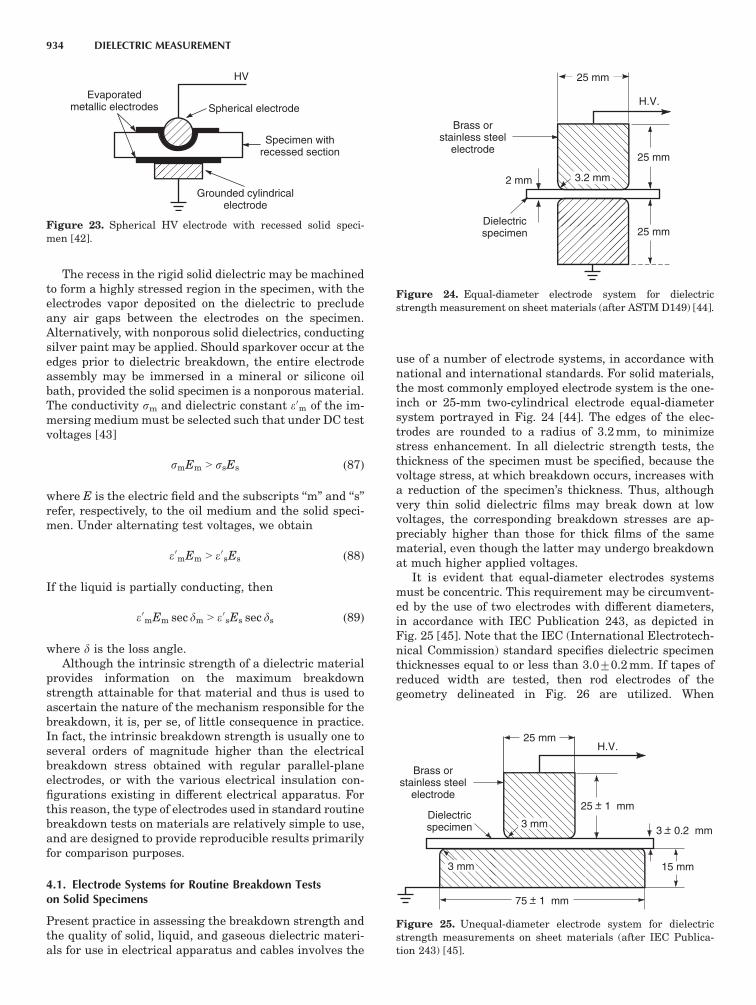
The recess in the rigid solid dielectric may be machinedto form a highly stressed region in the specimen, with theelectrodes vapor deposited on the dielectric to precludeany air gaps between the electrodes on the specimen.Alternatively, with nonporous solid dielectrics, conductingsilver paint may be applied. Should sparkover occur at theedges prior to dielectric breakdown, the entire electrodeassembly may be immersed in a mineral or silicone oilbath, provided the solid specimen is a nonporous material.The conductivity sm and dielectric constant e0m of the im-mersing medium must be selected such that under DC testvoltages [43]
smEm > ssEs ð87Þ
where E is the electric field and the subscripts ‘‘m’’ and ‘‘s’’refer, respectively, to the oil medium and the solid speci-men. Under alternating test voltages, we obtain
e0mEm > e0sEs ð88Þ
If the liquid is partially conducting, then
e0mEm sec dm > e0sEs sec ds ð89Þ
where d is the loss angle.Although the intrinsic strength of a dielectric material
provides information on the maximum breakdownstrength attainable for that material and thus is used toascertain the nature of the mechanism responsible for thebreakdown, it is, per se, of little consequence in practice.In fact, the intrinsic breakdown strength is usually one toseveral orders of magnitude higher than the electricalbreakdown stress obtained with regular parallel-planeelectrodes, or with the various electrical insulation con-figurations existing in different electrical apparatus. Forthis reason, the type of electrodes used in standard routinebreakdown tests on materials are relatively simple to use,and are designed to provide reproducible results primarilyfor comparison purposes.
4.1. Electrode Systems for Routine Breakdown Testson Solid Specimens
Present practice in assessing the breakdown strength andthe quality of solid, liquid, and gaseous dielectric materi-als for use in electrical apparatus and cables involves the
use of a number of electrode systems, in accordance withnational and international standards. For solid materials,the most commonly employed electrode system is the one-inch or 25-mm two-cylindrical electrode equal-diametersystem portrayed in Fig. 24 [44]. The edges of the elec-trodes are rounded to a radius of 3.2 mm, to minimizestress enhancement. In all dielectric strength tests, thethickness of the specimen must be specified, because thevoltage stress, at which breakdown occurs, increases witha reduction of the specimen’s thickness. Thus, althoughvery thin solid dielectric films may break down at lowvoltages, the corresponding breakdown stresses are ap-preciably higher than those for thick films of the samematerial, even though the latter may undergo breakdownat much higher applied voltages.
It is evident that equal-diameter electrodes systemsmust be concentric. This requirement may be circumvent-ed by the use of two electrodes with different diameters,in accordance with IEC Publication 243, as depicted inFig. 25 [45]. Note that the IEC (International Electrotech-nical Commission) standard specifies dielectric specimenthicknesses equal to or less than 3.070.2 mm. If tapes ofreduced width are tested, then rod electrodes of thegeometry delineated in Fig. 26 are utilized. When
Specimen withrecessed section
Spherical electrode
HV
Grounded cylindricalelectrode
Evaporatedmetallic electrodes
Figure 23. Spherical HV electrode with recessed solid speci-men [42].
25 mm
25 mm
25 mm
H.V.
2 mm
Brass orstainless steel
electrode
Dielectricspecimen
3.2 mm
Figure 24. Equal-diameter electrode system for dielectricstrength measurement on sheet materials (after ASTM D149) [44].
Brass orstainless steel
electrode
Dielectricspecimen
H.V.25 mm
15 mm
75 + 1 mm–
25 + 1 mm–
3 + 0.2 mm–3 mm
3 mm
Figure 25. Unequal-diameter electrode system for dielectricstrength measurements on sheet materials (after IEC Publica-tion 243) [45].
934 DIELECTRIC MEASUREMENT

breakdown tests are carried out on thin inorganic filmswith application to electron devices, miniature counterelectrodes are vapor deposited onto the surface of thespecimen. For the evaluation of embedding compoundsor greases, the standard procedure of ASTM D149 re-quires hemispherical electrodes, having an equivalent di-ameter of 12.7 mm [44].
The foregoing described electrode systems for solid di-electric specimens are suitable for tests under AC powerfrequency, DC, and impulse conditions. The electrode sys-tems, for routine determination of the dielectric strengthof liquids, differ from those described for solids. Routineacceptance tests on oils of petroleum origin for electricalapparatus and cables are carried out with an oil cup con-taining parallel-plane polished brass electrodes, with aninterelectrode spacing of 2.570.01 mm. The electrodeshave a diameter of 25 mm and a thickness of 3 mm; theyare square at the edges and are separated from the innerwall of the oil test cup by a distance of not less than13 mm. The oil test cup assembly is shown in Fig. 27 [46].The electrodes within the cell must be cleaned with a dryhydrocarbon solvent following each breakdown test; par-ticular care must be taken to remove any carbonization
deposits on the electrodes, and the electrodes must be re-polished should any pitting of the surface manifest. Priorto admitting the liquid specimen into a cleaned test cell,the latter must be rinsed by the same liquid to remove anyresidues of the cleaning compound.
It is palpably evident from the geometric configurationof the square-edge electrodes in Fig. 27, that electricalstress enhancement occurs at the edges of the electrodesand that, therefore, breakdown is likely to occur there. Forlower viscosity dielectric liquids (o19 cSt or mm2/s at401C), test electrodes, with the geometrical contour de-picted in Fig. 28, have been found to be particularly effec-tive in detecting decreases in the breakdown strength as aresult of cellulose fiber contamination and absorbed mois-ture [47]. These electrodes are normally referred to asVDE (Verband Deutscher Electrotechniker)-type elec-trodes. Measurements of dielectric strength are performedwith electrode separations of either 1 or 2 mm, with agentle downward oil flow at the electrodes created bymeans of a rotating impeller located beneath the elec-trodes in the test cell.
Since oil-filled and impregnated electrical power equip-ment is subjected to lightning and switching impulses, it isimportant to assess the quality of the oil in terms of itsimpulse breakdown strength. Under nonuniform electri-cal field conditions, the dielectric strength of the oil iscontingent on the polarity of the impulse in contradistinc-tion to negligible differences observed under uniformfields. For this reason, nonuniform field electrode systemsare frequently utilized for impulse tests. The electrodesmay typically consist of either two 12.7 mm diameter brassor steel spheres or, for highly nonuniform fields, one suchsphere and a steel needle point with a 0.06 mm radius ofcurvature at the needle tip [48].
The breakdown strength of gases is normally deter-mined under quasiuniform AC field conditions. Typicalelectrodes utilized for this purpose consist of a sphere-to-plane geometry, wherein the electrical field is uniformdirectly underneath the sphere adjacent to the plane, be-coming increasingly less uniform as the separationbetween the sphere and the plane increases. With asphere-to-plane geometry, electrical breakdown tends toalways occur in the uniform field region—that is, at thepoint where the separation between the sphere and theplane is least. The high-potential sphere electrode may
Brass or stainlesssteel cylindrical rods
0.8 mmradius
Dielectric tapespecimen
Figure 26. Cylindrical rod electrodes for dielectric strength mea-surements on thin narrow plastic tape or other narrow specimens(after ASTM D149) [44].
Brass disk electrodes
Plastic container
Gap adjustmentOil
25 mm
25 mm
3 mm≤
2.50 ± .01 mm
Figure 27. Parallel-plane square-edge electrode system for di-electric strength measurements on mineral oils (after ASTMD877) [46].
4 mmradius
Brass sphericallycapped electrodes
25 mmradius
13 mm
36 mm diameter
Figure 28. VDE electrode system for dielectric breakdownstrength measurements on low-viscosity liquids [47].
DIELECTRIC MEASUREMENT 935
be of steel with a diameter of 0.75 in. or 19.1 mm, and theground potential electrode may be a cylindrical brassplane with a 1.5 inch or 38.1 mm diameter [49]. The testsare performed at 251C at a standard pressure of 760 torr.
4.2. Voltage Breakdown Test Conditions and Procedures
The presence of lethal voltages in breakdown voltage testsnecessitates strict adherence to high-voltage safety prac-tices. Since the breakdown voltage may be a function ofthe ambient temperature, pressure, and humidity, de-pending on where solid, liquid, or gas specimens are test-ed, these parameters should be recorded at the time of thetest; solid insulating materials should be conditioned priorto the breakdown test, so that they may reach thermal andmoisture equilibrium with the environment. For morelossy solid and liquid specimens, the application of intensealternating electrical fields may result in cumulative heatgeneration due to dielectric losses, thereby leading to athermal instability induced breakdown. Solid specimensmay contain gas cavity inclusions, within which intenserecurring partial discharges at elevated alternating fieldsmay cause rapid deterioration of the adjacent solid insu-lation, thus leading to conspicuously lower breakdownstrengths. Both thermal and discharge mechanism asso-ciated breakdowns account for the lower observed ACbreakdown strengths, as opposed to those measured un-der DC and impulse conditions. Where the breakdownstrength is controlled by the thermal and partial dis-charge mechanism, the breakdown process is a strongfunction for the time of voltage application. Accordingly,the rate of voltage rise in any voltage breakdown test is animportant parameter.
For solid dielectrics, the rate of ac sinusoidal voltagerise is fixed usually at 500 V/s, though more rapid or slow-er rise rates may also be used. Breakdown or rupture ofthe dielectric is indicated by an audible voltage collapseacross the specimen, as well as a visual burn at the tip ofthe breakdown. In order to minimize stress-induced agingeffects in the insulation undergoing the voltage break-down test, ASTM D149 stipulates that the duration of ashort-time breakdown must not exceed 20 s. In the past, avoltage step test was employed, whereby the voltage wasraised in steps; at each step it was maintained for a presettime, prior to the next-step increment in voltage, until theensuence of dielectric breakdown event—that is, anabrupt voltage collapse across the specimen. The use ofthe step procedure was required in the absence of voltagesources with automatically regulated rate of voltage risecontrols.
In DC dielectric breakdown strength determinations ondielectric material specimens, a single rate of voltage riseof 500 V/s is employed [50]. Under direct voltages, the ini-tial breakdown event produces a minute channel in thevolume of the solid dielectric, whose trace is not readilydiscernible. Reapplication of the direct voltage results insuccessively lower breakdown voltages, which confirmthat a DC breakdown has already occurred. Also, the ad-ditional damage and burning produced within the break-down channel renders it more visible.
Impulse tests on solid dielectric specimens are per-formed by increasing the peak voltage of the impulsegradually, from an initial peak value of 0.7 times the an-ticipated breakdown voltage [45,50]. The lightning im-pulse is simulated with an impulse waveform having atime to peak of 1.2ms and a decay time of 50 ms to 50% of itsinitial peak value. Impulse breakdown is indicated by avoltage collapse at any point of the impulse waveform [2];the peak voltage value of this impulse wave is consideredas the impulse breakdown voltage. Location of the actualbreakdown channel caused by an impulse may require, asin the DC case, several reapplications of the voltage pulse,to cause additional carbonization within the breakdownchannel.
In the measurement of dielectric strength of liquidspecimens at AC power frequencies using the parallel-plane square-edge electrodes, a fixed voltage rise of 3 kV/sis generally specified [46]. To avoid pitting of the test elec-trode surfaces, the short-circuit current at breakdown inthe specimen is not permitted to exceed 10 mA/kV. Fortests with the same electrode system under direct voltag-es, the same rate of voltage rise should be adequate. Whenthe VDE-type electrodes are employed for low-viscosityliquids at power frequency, a much lower rate of voltagerise of 0.5 kV/s is preferred. Impulse breakdown tests per-formed on dielectric liquids are often carried out with boththe simulated lightning impulse of the 1.2 by 50 ms formand a switching surge impulse form with a 100ms risetimeto peak and a decay time 41000 ms. The impulse break-down tests are carried out either at positive or negativepolarities; often the measurements may be performed atboth polarities. The measurement sequence at either po-larity is begun at a voltage substantially below the ex-pected impulse voltage breakdown level. Normally, threeimpulse waves are applied at each selected impulse volt-age test level; it is an accepted practice to traverse at leastthree test levels prior to breakdown, with a fixed mini-mum time interval between each voltage level test. ASTMD3300 recommends a time interval of 30 s. The peak im-pulse voltage at breakdown is measured oscillographicallyacross a calibrated resistive voltage divider. Wheneverneedle electrodes are employed, the geometry of the nee-dle tip is altered, due to the energy released by the break-down spark; this necessitates a change of the needleelectrodes after each breakdown event.
Routine voltage breakdown strength measurements oninsulating gases are normally performed under AC powerfrequencies, using a standard rate of voltage rise of 500 V/s[49]. The breakdown strength of gases is a function of gapspacing and gas pressure; since the value of the lattervaries with the ambient temperature, both the pressureand temperature must be recorded for breakdown resultsobtained with a fixed gap setting.
It should be emphasized that, when the breakdownvoltages are determined for solid, liquid, and gas speci-mens, the gap length or specimen thickness must be stat-ed in each case. Even when the value of the voltagebreakdown strength is provided in the units of voltageper unit specimen thickness, the specimen thickness muststill be specified, because the breakdown strength is afunction of the specimen thickness. Also, the dispersion in
936 DIELECTRIC MEASUREMENT

the voltage breakdown data requires some form of statis-tical analysis. Breakdown strength data ordinarily refer toa mean measured value on 10 specimens. A low ratio (about0.1) of the standard deviation to the mean value, derivedfrom the ten measurements, is usually considered as anindicator of an acceptable probable error in the test results.
5. CONCLUDING REMARKS
The foregoing presentation of the measurement of con-ductivity, permittivity, and dielectric loss, and dielectricstrength of electrical insulating materials has attemptedto provide a concise cursory description of a number of themost common measurement techniques in use. Space lim-itations prevented a discussion on the various conductionand breakdown mechanism and their influence on themeasured quantities. For a more in-depth discussion onthe mechanisms involved and their determining inferenceon the measured quantities obtained with a variety of dif-ferent test methods, the reader is referred to other liter-ature [2,18,20,42].
BIBLIOGRAPHY
1. R. Bartnikas, Dielectrics and insulators, in R. Dorf, ed., The
Electrical Engineering Handbook, CRC/IEEE Press, Boca Ra-ton, FL, 1997, Chap. 55.
2. R. Bartnikas, ed., Engineering Dielectrics, Vol. IIB, ElectricalProperties of Solid Insulating Materials: Measurement Tech-
niques, STP926, ASTM, Phildelphia, 1987.
3. ASTM D257, Standard Test Methods for D-C Resistance or
Conductance of Insulating Materials, Annual Book of ASTMStandards, Vol. 10.01, Philadelphia, 1997.
4. IEC Publication 93, Methods of Test for Volume Resistivity
and Surface Resistivity of Solid Electric Insulating Materials.
5. ASTM D374, Standard Test Methods for Thickness of Solid
Electric Insulation, Annual Book of ASTM Standards, Vol.10.01, Phildelphia, 1997.
6. Low Level Measurements, 4th ed., Keithley Instruments,Cleveland, OH, 1993.
7. B. V. Hamon, An approximate method for deducing dielectricloss factor from direct current measurements, Proc. IEE99:151–155 (1952).
8. H. Block et al., Treatment of data in step-response, dielectricrelaxation measurements, J. Chem. Soc. Faraday Trans. II
68:1890–1896 (1972).
9. H. St-Onge, Electrical conduction in 3-percent carbon filledpolyethylene—Part I: Low field results, IEEE Trans. Electric
Insul. EI-11:20–27 (1976).
10. P. J. Hyde, Wide-frequency range dielectric spectrometer PartII, Proc. IEE 117:1891–1901 (1970).
11. F. I. Mopsik, Precision time-domain dielectric spectrometer,Rev. Sci. Instrum. 55:79–87 (1984).
12. A. M. Thompson, A bridge for the measurement of permit-tivity, Parts B and C, Proc. IEE 103:705–709 (1955).
13. W. P. Harris, Operators Procedures Manual for the HarrisUltra-Low Frequency Impedance Bridge, National Bureau ofStandards Report 9627, Washington, DC, 1968.
14. R. J. Kriegler and R. Bartnikas, Dielectric loss and current-voltage measurements in sodium-contaminated Si-SiO2–Cr
structures, IEEE Trans. Electron. Devices ED-20:722–731
(1973).
15. J. Pugh, Proc. 4th Int. Conf. Dielectr. Mater. Meas. Appl., IEEConf. Publ. 239, Lancaster, UK, Sept. 10–13, 1984, pp. 247–249.
16. ASTM D150, Standard Test Methods for AC Loss Character-
istics and Permittivity (Dielectric Constant) of Solid Electrical
Insulating Materials, Annual Book of ASTM Standards,
Vol. 10.01, 1998.
17. H. J. Wintle and S. Kurylowicz, Edge corrections for strip anddisc capacitors, IEEE Trans. Instrum. Meas. IM-34:41–47
(1985).
18. R. Bartnikas, ed., Engineering Dielectrics, Vol. III, ElectricalInsulating Liquids, Monograph 2, ASTM, Philadelphia, 1994.
19. R. Bartnikas and K. D. Srivastava, eds., Power Cable Engi-
neering, Sandford Fleming, Waterloo, Ontario, 1987.
20. R. Bartnikas and E. J. McMahon, eds., Engineering Dielec-
trics, Vol. I, Corona Measurement and Interpretation, STP
669, ASTM, Philadelphia, 1979.
21. A.G. Tettex, Prazisions-Verlustfactor und Kapazitats MeB-rucke Typ 2821, Prospekt 2821, Blatt 103, Zurich 1980.
22. O. Petersons, A self-balancing high voltage capacitancebridge, IEEE Trans. Instrum. Meas. IM-13:216–224 (1964).
23. Bridges/Standards, Gen Rad Bulletin JN 4240-681, Gen Rad,Boston, MA.
24. P. Osvath and S. Widmer, A high-voltage high-precision self-balancing capacitance and dissipation factor-measuring
bridge, IEEE Trans. Instrum. Meas. IM-35:19–23 (1986).
25. ASTM D1531. Test for Dielectric Constant and Dissipation
Factor of Polyethylene by Liquid Displacement Procedure,
Annual Book of ASTM Standards, Vol. 10.01, 1997.
26. L. Hartshorn and W. H. Ward, The measurement of the per-mittivity and power factor of dielectrics at frequencies from
104 to 108 cycles per second, J. IEE 79:597–609 (1936).
27. W. Reddish et al., Precise measurement of dielectric proper-ties at radio frequencies, Proc. IEE 118: 255–265, (1971).
28. K. A. Buckingham and J. W. Billing, Proc. 3rd Int. Conf.
Dielectric Measurement Applications, Birmingham, England,
Sept. 10–13, 1979, pp. 392–395.
29. T. V. L. Parry, The measurement of permittivity and powerfactors of dielectrics at frequencies from 300 to 600 c/s, part
III, J. IEE 98:303–311 (1951).
30. S. Roberts and A. von Hippel, A new method for measuringdielectric constant and loss in range of centimeter waves,
J. Appl. Phys. 17:610–616 (1946).
31. W. B Bridges, M. B. Klein, and E. Schweigh, Measurement ofdielectric constant and loss tangent of thallium mixed halide
crystals KRS-5 and KRS-6 at 95 GHz, IEEE Trans. Microwave
Theory Tech. MTT-30:286–292 (1982).
32. ASTM D2520, Test Methods for Complex Permittivity of Solid
Electrical Insulating Materials at Microwave Frequencies and
Temperatures to 16501C, Annual Book of ASTM Standards,
Vol. 10.01, 1998.
33. W. B. Westphal, Distributed circuits, in A. von Hippel, ed.,Dielectric Materials and Applications, Wiley, New York, 1954,
Chap. 2, Sect. A2.
34. T. W. Dakin and C. Works, Microwave dielectric measure-ments, J. Appl. Phys. 18:789–796 (1947).
35. A. C. Lynch, Transmission methods for measurement of di-electric loss, Conf. High Frequency Dielectr. Meas., Natl. Phys-
ical Laboratory, Teddington, UK, March 27–29, 1972.
36. IEC Publication 377-2, Measurement of Permittivity and Loss
at Frequencies above 300 MHz.
DIELECTRIC MEASUREMENT 937

37. A. H. Sharbough and S. Roberts, Dielectric measurementprocedures, in K. Lark-Horowitz and V. A. Johnson, eds., Sol-id Slate Physics, Vol. VI, Part B, Academic Press, New York,1959, Chap. 7, Sect. 71.
38. W. Culshaw, A spectrometer for millimetre wavelengths, Proc.
IEE, Part IIA, 100:5–14 (1953).
39. J. E. Degenford, A quasi-optic technique for measuring di-electric loss tangents. IEEE Trans. Instrum. Meas. IM-17:413–417 (1968).
40. J. Chamberlain, Submillimetre-wave techniques, Conf. HighFrequency Measurement, Natl. Physical Laboratory, Ted-dington, UK, March 27–29, 1972.
41. J. R. Birch et al., An intercomparison of measurement tech-niques for the determination of the dielectric properties ofsolids at near millimeter wavelengths, IEEE Trans. Micro-wave Theory Tech. 42:956–965 (1994).
42. J. K. Nelson, in R. Bartnikas and R. M. Eichhorn, eds.,Engineering Dielectrics, Vol. IIA, Electrical Properties of
Solid Insulating Materials: Molecular Structure and ElectricalBehavior, STP 783, ASTM, Philadelphia, 1983.
43. S. Whitehead, Dielectric Breakdown of Solids, ClarendonPress, Oxford, 1953.
44. ASTM D149, Test Method for Dielectric Breakdown Voltage
and Dielectric Strength of Electrical Insulating Materials atCommercial Power Frequencies, Annual Book of ASTM Stan-
dards, Vol. 10.01, 1997.
45. IEC Publication 60, 243, Parts 1–3, Electric Strength of In-
sulating Materials—Test Methods.
46. ASTM D877, Standard Test Method for Dielectric BreakdownVoltage of Insulating Liquids Using Disk Electrodes, Annual
Book of ASTM Standards, Vol. 10.03, 1997.
47. ASTM, D1816, Standard Test Method for Dielectric Break-
down Voltage of Insulating Oils of Petroleum Origin UsingVDE Electrodes, Annual Book of ASTM Standards, 1997,Vol. 10.03; see also VDE (Verband Deutscher El-ektrotechniker) Specification 0370.
48. ASTM D3300, Standard Test Method for Dielectric Break-down Voltage of Insulating Oils of Petroleum Origin under
Impulse Conditions, Annual Book of ASTM Standards,Vol. 10.03, 1997.
49. ASTM D2477, Standard Test Method for Dielectric Strength
of Insulating Gases at Commercial Power Frequencies, Annu-al Book of ASTM Standards, Vol. 10.03, 1997.
50. ASTM D3755, Test Method for Dielectric Breakdown Voltage
and Dielectric Strength of Solid Electrical Insulating Materi-
als under Direct Voltage Stress, Annual Book of ASTM Stan-dards, Vol. 10.02, 1997.
DIELECTRIC PERMITTIVITY AND LOSS
D. K. DAS-GUPTA
University of WalesBangor, Wales
Dielectrics can be defined as materials with high electricalresistivities that conduct virtually no electricity at low DCelectric fields. A large group of materials, including gases,liquids, semiconductors, ceramics, and organic and inor-ganic polymers, are classified as dielectrics. There are,however, no perfect dielectric materials.
The study of the electrical properties of dielectrics aris-es from their practical need for efficient electrical insula-tion requirements for long operational life. Manydielectric materials are classified by their electrical break-down strength, dielectric loss, permittivity, and polariza-tion, and these macroscopic properties are related to theiratomic and molecular structures. Although dielectrics arewidely employed in diverse applications (e.g., capacitors,cables, transformers, motors), the study of dielectrics hasprogressed very little since the early investigation of fer-roelectric phenomena. However, the advent of microelec-tronics and complex control devices and components indefense and industrial applications has made dielectricresearch important in its own right.
The present article briefly reviews the electrostaticconcepts that lead to time- and frequency-dependent di-electric phenomena together with the models of dielectricrelaxation behavior in various materials. It also includessome explanations for the dielectric aging of insulatingmaterials under high fields in humid environments.
1. DIELECTRIC POLARIZATION
1.1. Static Field
When an electric field is applied to a dielectric material,three processes can occur:
1. A steady flow of direct current (due to the DC con-ductivity s0) may occur if free charges are capableof moving throughout the volume without restraint.
2. Bound charges can form dipoles by aligning with thefield and provide polarization. On removal of thefield the dipoles may return to their original randomorientations with the help of thermal energy, givingrise to dielectric relaxation.
3. Electronic and ionic charges may hop through thedefect sites. These charges are neither free norbound, and they give rise to an intermediate formof polarization, which involves finite charge storage.
Dielectrics may broadly be divided into nonpolar andpolar materials. In nonpolar materials in an external fielda dielectric polarization occurs when the positive and neg-ative charges experience an electrical force that causesthem to move apart in the direction of the external field.As a result, the centers of positive and negative charges nolonger coincide. The molecules are then said to be pola-rized, and each molecule forms a dipole and acquires adipole moment p, defined thus
p¼ e dl ð1Þ
where e is the electronic charge and dl the displacement(B1010–1011 m in magnitude) between the two chargecenters. Note that dl is a vector that points from the neg-ative to the positive charge. Such dipoles are called in-duced dipoles. On removal of the field, the charges areredistributed and the dipole moment vanishes.
938 DIELECTRIC PERMITTIVITY AND LOSS

With polar dielectrics, which lack structural symmetry,the charge centers of opposite polarities do not coincide fora molecule even in the absence of an electric field. Howev-er, these molecular dipoles may be randomly distributed,thus summing to a zero dipole moment over any macro-scopic volume element [1–9]. In the presence of an appro-priate electric field, the molecules may align themselves inthe field direction and thus provide a net dipole moment.
Macroscopically, the electric field in a dielectric is de-scribed [2] by the electric field strength E (V/cm) and theelectrical displacement density, also known as the electricflux density, D (C/m2), where both D and E are vectorquantities. Now the polarization can be defined as thedipole moment per unit volume, namely
P¼X
N
i¼ 1
pi=Dn ð2Þ
and is also a vector quantity. It should be noted that thenormal component of P at the surface equals the surfacecharge density per unit area. These three vectors, D, E,and P, in a material medium other than vacuum, arerelated thus
D¼ e0EþP ð3Þ
or
D¼ eE ð4Þ
where
e¼ e0er ð5Þ
where e0 is the permittivity in free space (8.85 1012 F/m) and er is the relative permittivity (dimensionless) orthe dielectric constant of the material, which takes intoaccount the polarization effect and is defined as
er¼C
C0ð6Þ
where C0 is the capacitance of a capacitor with a vacuumbetween two conductors and C the capacitance when thesame region is filled with the dielectric. er is independentof the shape or size of the conductors and is entirely acharacteristic of the particular dielectric medium. Table 1[4] gives the values of er for static or low-frequency (o1-kHz)fields of several materials. er, which is a macroscopic anddirectly measurable parameter, is connected with the mi-croscopic structure of a dielectric material and with itspolarization behavior.
From Eq. (3), we have
D¼ e0 1þP
e0E
E
¼ e0ð1þ wÞE
¼ e0erE
ð7Þ
where
er¼1þ w and w¼P
e0Eð8Þ
and w is the dielectric susceptibility. Thus the parameter walso provides a link between the macroscopic propertiesand the atomic molecular theory of dielectric materials.
We may also write a general relation between P and Ethus (8)
P¼ ewEþhigher terms in E ð9Þ
where the higher terms in E are applicable to the phe-nomenon of hyperpolarization. It should be noted that w isthe ratio of bound charge density to free charge density ofa capacitor. A measurement of er and hence w provides themagnitude of the polarization P of a dielectric material atany particular field E.
One of the most useful methods of determining P isto measure the current density J(t) as a function of time,as [8]
JðtÞ¼dD
dtð10Þ
It may be shown [3,8] that for noninteracting dipoles, wis given by
wð0Þ¼NP2
3e0kTð11Þ
Table 1. The Relative Permittivity of Some SolidDielectrics at 251C
Dielectric er
Vacuum 1 (by definition)Air (atmospheric pressure, 01C) 1.0006Amber 2.7Borosilicate glass 4.0Corning glass 0010 6.68Corning glass 0014 6.78Pyrex glass 4–5Quartz (fused) 3.8Diamond 5.5Porcelain 5.5Marble 10–15Mica 6–11Steatite 6Polyethylene 2.25Polyvinylchloride (PVC) 6Epoxy resin 3.6–11Rubber 3–4Neoprene 7Beeswax (white) 2.65Beeswax (yellow) 2.73Paraffin wax 2.3Barium titanate 1200
Source: Ref. 4.
DIELECTRIC PERMITTIVITY AND LOSS 939

where w(0) is the static susceptibility in the zero-frequencylimit, N the number density of polarizable molecules, k theBoltzmann constant, and T the temperature. w is a dimen-sionless and scalar quantity in an isotropic medium.
2. MICROSCOPIC CONCEPTS OF POLARIZATION
We shall consider here the three cases of electronic, ionic,and orientational polarizations.
An isolated neutral atom in an electric field acquires adipole moment when an external electric field produces aseparation of the charge centers of opposite polarities.This is known as the electronic polarization, and it pro-vides an induced dipole moment
pind¼ aeE ð12Þ
where ae is the electronic polarizability of an atom and isgiven by
ae¼ 4p e0r30 ð13Þ
where r0 is the radius of the spherical of an electron cloudsurrounding an atomic nucleus. The molar polarizabilityP of a monoatomic gas is given by
P¼N04p3
r30 ð14Þ
where N0 is the number of molecules in a gram molecule(Avogadro’s number). The lowest polarizability belongs tothe noble gases with their completely filled outer electron-ic shells, which screen the nuclei from the effect of the ex-ternal electric field. For hydrogen, with r0¼ 0.5310 10 m, ae is 1.66 1041 F/m2. Hence for a field E of105 V/m1, aE¼ 10 36 C/m. The length l of this induced di-pole is p/e¼ 1017 m (where e is the electronic charge),which is indeed an extremely small distance comparedwith atomic dimensions [6].
Ionic polarization occurs in ionic substances, such asalkali halides, whose molecules are formed of atoms thathave excess charges of opposite polarities. In an externalfield the relative positions of the positive and negative ionsof a molecule may shift, thus introducing the dipole mo-ment in addition to the induced electronic polarization.The ionic polarization pi is given by
pi¼ aiE ð15Þ
where ai is the ionic polarizability of the molecule, whicharises from the ionic displacement. The alkali halides (ha-lides of the group I elements) have the highest polariz-abilities, possibly because of the single electron in theiroutermost shells. Table 2 [6] provides a list of values ofcontribution of ions to the molar polarization of typicalalkali halides.
The third type of polarization, known as the orienta-tional polarization, is associated with permanent dipolesin dipolar materials that possess a dipole moment even inthe absence of an externally applied electric field. However,
such a moment may not be observed macroscopically, asthe thermal energy will randomize the dipoles so that theaverage moment will be zero over a small physical volume.On an application of an external electric field the dipoleswill experience a torque, which will orient them in thefield direction so that the average dipole moment will nolonger be zero. It may be shown [3] that the orientationalpolarizability a0 is given by
a0¼p2
3kTð16Þ
By adding the three polarizabilities mentioned above,the total polarization P can now be written as the sum ofthe three components
P¼peþpiþp0¼N aeþ aiþp2
o
3kT
E ð17Þ
where N is the number of contributing molecules or par-ticles per unit volume.
Of course, not all atoms or molecules need displayeach of these three types of polarizability. Only theorientational polarization is temperature-dependent.Equation (17) is known as the Langevin–Debye formula,and we have
w¼ er 1¼P
e0E¼
N
e0aeþ aiþ
p2o
3kT
ð18Þ
Thus a measurement of er as a function of temperaturemay help to distinguish the orientational polarization con-tribution from the sum of the components ae and ai, whichare practically independent of temperature.
Figure 1 shows (9) a plot of er1 as a function of 1/T forthe molecule of methyl amine (CH5N). The intercept forthe line at 1/T¼ 0 and its slope are approximately 8104 and 0.6 K 1, respectively. From Eqs. (8), (9), and(17), we have (9)
aeþ ai¼8 104e0
N 6 104F=m2 ð19Þ
Table 2. Ionic Polarization as a Fraction of the TotalPolarization for Alkali Halides, and (in Parentheses)the Ionic Polarization of Each Compound Relative to thatof LiF
F Cl Br I
Li 0.68 (1.0) 0.53 (3.22) 0.49 (1.96) 0.40 (2.09)Na 0.65 (1.12) 0.50 (3.38) 0.44 (1.82) 0.39 (2.13)K 0.65 (1.95) 0.49 (4.25) 0.46 (2.38) 0.38 (2.34)Rb 0.62 (2.19) 0.52 (5.14) 0.44 (2.46) 0.38 (2.62)
Source: Ref. 6.
940 DIELECTRIC PERMITTIVITY AND LOSS
and
p2o ¼
0:6eo3k
N 4:2 1030 C=m ð20Þ
The further separation of ae and ai is not possible usingthis technique alone.
Table 3 gives the electric dipole moments of some mol-ecules. The commonly used unit of dipole moment is thedebye; 1 D¼ 3.33 1030 C/m.
Space charge (interfacial) polarization generally arisesfrom a presence of electrons and/or ions that have limitedmacroscopic motions in the bulk of a dielectric material.Eventually these charge carriers are localized at latticedefect sites, metal–electrode interfaces, impurity centers,and voids. As a result, the electric field in the dielectricmay become distorted, thus producing an apparentincrease in the dielectric constant. Space charge polariza-tion is particularly evident in multiphase and inhomoge-nous dielectrics, and its effect is dominant, particularly atlow frequencies, in practical dielectrics such as impreg-nated paper, polymers, and sintered ceramics.
The study of dielectric polarization and susceptibilityin liquids and solids is more complicated than in gasesbecause of the interactions between the atoms and mole-cules in the condensed phase. These atoms and moleculeswill still exhibit electronic, ionic, and orientational polar-izations. However, the effective local field E1 on an atom ormolecule in a liquid or a solid dielectric may not be thesame as the externally applied field E. It is difficult to cal-culate the effective local field E1 in the condensed phaseexcept for the most symmetric crystals.
Since P¼ e0 (er 1) E, for the simplest case of a cubiccrystal, the Lorentz equation for the local field El (6) is
E1¼ ðerþ 2ÞE=3 ð21Þ
and P¼NaEl, where a is the total polarizability and N thenumber of molecules per unit volume. Hence
P¼ ðerþ 2ÞNE=3 ð22Þ
and
Na3e0¼
er 1
erþ 2ð23Þ
Equation (23) is the Clausius–Mossotti equation, whichrelates the microscopic property of the polarizability awith the macroscopic property of the relative permittivityor dielectric constant er. Now we have
N¼N0rM
ð24Þ
where N0 is the Avogadro number, M the molecularweight, and r the density. Substituting Eq. (24) intoEq. (23), we obtain the molar polarizability per mole:
N0a3e0¼
M
rer 1
erþ 2ð25Þ
Equation (25) should be used with caution, as it does nottake dipolar interactions into account properly. Equation (23)may, however, be used to calculate the electronicpolarizability ae from the measured values of er for dilutegases, for which erE1 and erþ 2E3. For such cases, wehave
ar¼e0ðer 1Þ
N¼
e0wN
ð26Þ
T
1/T (K)
Methylamine
0
0.001
0.002
0.003
600 300 100°C
0 0.001 0.002 0.003
r −
1
Figure 1. A plot of er1 as a function of 1/T for a molecule ofmethylamine (CH5N) [9,10].
Table 3. Electric Dipole Moments of Some Molecules
Dipole moment
Molecule (1030 C/m) (D)
HCl 3.5 1.05CsCl 35.0 10.5H2O 6.2 1.87D2O 6.0 1.80NH3 4.9 1.47HgCl2 0.0 0CCl4 0.0 0CH4O 5.7 1.71
DIELECTRIC PERMITTIVITY AND LOSS 941

Table 4 shows that the polarizability of the element ar-gon does not vary significantly [9] between its dilute gasand liquid states. That may not be true for other gaseswith more extensive electronic structure when condensedto liquid or solid form.
The polarizabilities of ae and ai may be determined in-dependently for ionic crystals in the solid state. The rel-ative permittivities er of ionic crystals are frequency-dependent. For an applied field at low frequencies the val-ue of er will be dependent on both ae and ei, whereas in theoptical frequency range the lattice ions will not be able tofollow the applied field and er will only be ee. Table 5 showsthe static (low-frequency) and optical (high-frequency)values of er for some ionic crystals [9]. The difference be-tween the values of er in the second and the third columnsis the contribution of the ionic polarization alone, whereasthose in the third column characterize the contributiondue to ae.
The behavior of orientational polarization in dipolarmolecules in the gas and liquid phases may be quite largeif rotation of the dipoles is possible [10]. For such a case,the polarizability will have contributions from ae, ai, anda0, where the a0 contribution will be temperature-depen-dent, where er increases with decreasing temperature.However, as the temperature is lowered and the materi-al solidifies, the value of er will drop abruptly when themolecules can no longer rotate, and thus rotation cannotcontribute to the polarization. Figure 2a [9,11] illustratessuch behavior of er for nitromethane. It may be observedthat at 244 K, nitromethane freezes and er drops abruptlyfrom 45 to just under 5. At this temperature a0 is zero fornitromethane and its polarizability arises from the ae andai contributions, which are independent of temperature.However, there are some solids, such as HCl, that do notshow this type of behavior. For HCl in the liquid state er islarge and increases with decreasing temperature, indicat-ing rotational behavior of the molecules (see Fig. 2b).However, below 165 K, where HCl freezes, er still contin-ues to increase [9,12] because of the increase in the den-
sity of the material. At 100 K, the molecular rotationfinally ceases and a0 virtually becomes zero. The polariza-tion contribution at this temperature in HCl originatesfrom ae and hindered rotation [9,12].
3. DIELECTRIC LOSS
3.1. Time-Dependent Dielectric Response
The dielectric behavior has been represented in the pre-vious section by three vectors, D, E, and P, which are as-sumed to be collinear in space and in the same phase intime. However, neither of these two assumptions is nec-essarily valid. We shall only consider the nature of the di-electric behavior with time for nonpolar materials andthose containing permanent dipoles. Regarding the spa-tial collinearity, extensive treatment of crystal symmetryis necessary and will not be discussed here.
The time-dependent dielectric response may be synthe-sized [8] from three fundamental time dependences of theelectric field: the delta function d(t), the step function 1(t),
Table 4. Polarizability of Argon
Form T (K) Pressure (atm) er ae (10 40 F/m2)
Gas 293 1 1.000517 1.83Liquid 83 1 1.53 1.86
Source: Ref. 9.
Table 5. Static and Infinite-Frequency Capacitivity ofSome Ionic Crystals
er
Material Static Optical
LiF 9.27 1.90LiC 11.05 2.68NaCl 5.62 2.32KCl 4.64 2.17RbCl 5.10 2.18NaI 6.60 2.96
Source: Ref. 9.
180 220 260 300
60 80 100 120 140 160 180
T (K)
Melting temperature
HCI
f = 300 Hz
T (K)
50
40
30
20
10
0
Nitromethanef = 70,000 Hz
Meltingtemperature
r
50
40
30
20
10
0
r
(a)
(b)
Figure 2. The behavior of er versus T for completely hindered (a)and partly hindered (b) rotation of dipoles in the solid: (a) nitro-methane [9,11]; (b) hydrogen chloride [9,12].
942 DIELECTRIC PERMITTIVITY AND LOSS

and the harmonic function sin o(t) or cos o(t), where o isthe angular frequency (¼ 2pf). Equation (3) may now berepresented thus
DðtÞ¼ e0EþPðtÞ
where the first term on the right-hand side provides theinstantaneous free-space contribution and the second thedelayed polarization. We define a dielectric response func-tion f(t). The polarization response to a delta function ex-citation of strength E Dt is [8]
PðtÞ¼ e0ðEDtÞfðtÞ ð27Þ
where E is the electric field, acting over a time period DT.From the principle of causality, we have
fðtÞ¼ 0 for to0 ð28Þ
In the absence of any permanent polarization, we obtain
limt!1
fðtÞ¼ 0 ð29Þ
Furthermore, from the principle of superposition, wehave [8]
PðtÞ¼ e0
Z t
1
fðt tÞEðtÞdT ð30Þ
Equation (30) implies that the magnitude of polariza-tion at a time t in a dielectric will depend on its past value;in other words, the material has a memory. On an appli-cation of an elementary step function field E1(t), thedielectric polarization is given by
PðtÞ¼ e0E
Z t
0fðtÞdt ð31Þ
The charging current Ic(t) is given by [8]
IcðtÞ¼dDðtÞ
dtþ s0E
¼ e0dEðtÞ
dtþ
dPðtÞ
dtþ s0E
ð32Þ
¼ e0E½dðtÞþfðtÞ þ s0E ð33Þ
where the delta function d(t) represents the instantaneousfree-space response of the step function field, followed bythe polarization current dP(t)/dt of the material. s0 is theDC conductivity, if any, of the dielectric at infinitely longtime. Thus, we have [8]
Pð1Þ¼ e0E
Z 1
0fðtÞdt¼ e0wð0ÞE ð34Þ
where P(N) is the polarization with a steady electric fieldE after an infinitely long time when the polarizing ele-ments tend to be oriented along the field direction. On
removal of this step function field, a depolarization cur-rent Id(t) will follow as the thermal agitation randomizesthe orientation of the dipoles with time. For this lattercase there will be no contribution of s0 at E¼ 0.
3.2. Frequency-Dependent Dielectric Response
The polarization response to a harmonic field is known asthe frequency-domain response. Taking the Fourier trans-form of both sides of Eq. (34), we get
PðoÞ¼ e0wðoÞEðoÞ ð35Þ
where P(o) and E(o) are the Fourier transforms of thetime-dependent polarization and field, respectively. w(o) isthe frequency-dependent complex susceptibility, and it isthe Fourier transform of the time-dependent responsefunction f(t):
wðoÞ¼ w0ðoÞ iw0 0ðoÞ¼Z 1
0fðtÞeiot dt ð36Þ
The real part w0(o) provides the magnitude of polariza-tion in phase with the harmonic driving field E(o) anddoes not contribute to the power loss, whereas the imag-inary part w00(o), which is in quadrature with the field, isreferred to as the dielectric loss. w0(o) and w00(o) may berepresented as odd and even functions of frequency, re-spectively:
w0ðoÞ¼Z 1
0fðtÞ cos ot dt ð37Þ
w0 0ðoÞ¼Z 1
0fðtÞ sin ot dt ð38Þ
In terms of permittivity, we may write
DðoÞ¼ eðoÞEðoÞ¼ e0½1þ w0ðoÞ iw0 0ðoÞEðoÞ ð39Þ
For zero frequency, namely, the static case, we have
w0ð0Þ¼Z 1
0
fðtÞdt ð40Þ
and
w0 0ð0Þ¼ 0 ð41Þ
Equation (36) shows that both w0 (o) and w00(o) are func-tions of the dielectric response function f(t), and these twoparameters are Hilbert transforms of each other, throughwhat are referred to as the Kramers–Kronig relations:
w0ðoÞ¼1
PC
Z 1
1
w0 0ðoÞx o
dx ð42Þ
w0 0ðoÞ¼ 1
PC
Z 1
1
w0ðxÞx o
dx ð43Þ
DIELECTRIC PERMITTIVITY AND LOSS 943
where C denotes the Cauchy principal value of the inte-gral. For the static case
w0ð0Þ¼2
p
Z 1
1
w0 0ðxÞd ln x ð44Þ
Equation (44) indicates that the variation of the dielec-tric parameters with frequency, specifically, the dielectricdispersion, is an essential property of dielectric materials[8]. It also shows that any mechanism that can lead to astrong polarization in a dielectric material must also leadto large losses in some frequency range. In other words, itis not possible to have a loss-free dielectric with a finitesusceptibility [8]. In most dielectrics the loss is significantonly in limited frequency ranges. Figure 3 [8] shows sche-matically two nonoverlapping loss processes at the lowfrequencies and a resonance process in the optical fre-quency range. In a limited frequency region we may definea high-frequency permittivity eNa, accounting for allthe processes occurring at higher frequencies; thus [seeEq. (39)]
eðoÞ¼ e1aþ e0½wa0ðoÞ iwa
0 0ðoÞ ð45Þ
from which we get
ea 0ðoÞ¼ e1aþ e0wa0ðoÞ ð46Þ
and
ea 0 0ðoÞ¼ e0wa0 0ðoÞ ð47Þ
For an alternating voltage the frequency-dependentcomplex capacitance C(o) is
CðoÞ¼C0ðoÞ iC0 0ðoÞ ð48Þ
where C0(o) and C00(o) are the real and imaginary parts ofthe complex capacitance. The loss angle d is the angle be-tween the electric field and the dielectric polarization. The
loss tangent
tan d¼C0 0ðoÞC0ðoÞ
¼e0 0ðoÞe0ðoÞ
ð49Þ
is independent of the geometry of the dielectric material.The existence of the polarization with respect to the
field leads to the energy dissipation in the dielectric. Nowthe power dissipation P per unit volume is
P¼ IphaseE
where Iphase is the part of the current in phase with E, andis given by
P¼oE2e0e0 tan d¼oE2e0e0 0 ð50Þ
Table 6 gives (6) typical values of the permittivity andloss factor of various dielectric materials at room temper-ature for different frequencies. Generally polar materialshave larger permittivities and loss tangents than do non-polar materials. For many liquids the frequency at whichmaximum energy loss occurs at room temperature is ap-proximately 1000 MHz (wavelength lE0.3 m), as shown[1] for three typical liquids in Table 7, where t is therelaxation time (¼ 1/f).
Another type of energy loss occurs in a resonance ab-sorption process at very high (i.e., IR, visible, and UV)frequencies. Although the real and imaginary parts of thecomplex permittivity vary in a manner similar to that fordipole relaxation, the origin of the energy loss is differentin this process. At optical frequencies the permittivity ofthe dielectric is due almost entirely to the electronic po-larization. In the absence of any external field a vibratingelectron of charge e and mass m is elastically bound to itsnucleus by a restoring force, and its equation of motion is
md2x
dt2þ kx¼ 0 ð51Þ
where k is the restoring-force constant and x is the dis-placement of the electron. This equation represents a sim-ple harmonic motion, and its solution is
x¼ x0 sin o0tþA ð52Þ
where o0¼ (k/m)1/2, A is the integration constant, x0 theamplitude of oscillation, and o0 the natural resonance an-gular frequency of the oscillation. When an external al-ternating electric field is applied to this system, theresulting motion is a forced oscillation, represented by
md2x
dt2þmo2
0x¼ e E cos ot ð53Þ
where E is the amplitude of the field E and o is its fre-quency. Clearly the response of the oscillating system willnow depend on both o and o0. The oscillations might beexpected to build up without limit when o¼o0, althoughthey are expected to be small at frequencies far away from
r(0
)
r∞
r∞1
r∞1
,r
∆′1
′1
′2′3
′′3′′2′′1
log
p1 p2 p3
Figure 3. Schematic diagram of the frequency dependence of thereal and imaginary parts of the complex susceptibility, showingthree processes; the last one is a resonance process [8].
944 DIELECTRIC PERMITTIVITY AND LOSS
o0. However, at resonance (i.e. o¼o0), the oscillationswill in fact be limited (damped) by the emission of elec-tromagnetic radiation by the oscillating charges, whichdissipates energy. It may be shown that in a resonanceabsorption process [6]
e0ðoÞ¼ e0þNe2
m
o20 o2
ðo20 o2Þþ r2o2
ð54Þ
and
e0 0ðoÞ¼Ne2
m
roðo2
0 o2Þþ r1o1ð55Þ
where r is a constant of the material, called the dissipationconstant. These quantities have the form shown in Fig. 3at very high frequencies. For o¼ 0, which is the staticcase, we have
e0ð0Þ¼ e0þNe2
mo20
ð56Þ
e00(o) approaches zero for both oco0 and oo0, and itgoes through a maximum value of Ne2(1/mro). Again e00(o)represents an energy loss and the power loss P is givenagain by
P¼oe0 0ðoÞe0E2ð57Þ
As the characteristic values of o0 for electron clouds arevery high, the resonance absorptions and their corre-sponding energy losses occur at very high frequencies inthe IR–UV range.
For pure nonpolar dielectrics, whether solid, liquid,or gas, the polarization is of an essentially electronicnature. Some polar materials with a highly symmetricstructure, like carbon tetrachloride (CCl4), may also
Table 6. Dielectric Properties of Materials
Relative permittivity er
Material Direction f¼60 Hz 100 kHz 1 MHz 100 MHz Loss tangent tan d
Crystals
Rutile, TiO2 8c — 170 170 — 10 4
>c 90 90 — 2104
Aluminum oxide, Al2O3 8c — 10.6 10.6 10.6 —>c 8.6 8.6 8.6 —
Lithium niobate, LiNbO3 8c — — 30 — 0.05>c — 75 — —
Ceramics
BaTiO3 — — 1600 — 15010 4
Alumina — — 4.5–8.5 — 0.0002–0.01Steatite — — 5.5–7.5 — 0.0002–0.004Rutile — — 14–110 — 0.0002–0.005Porcelain — — 6–8 — 0.003–0.02
Polymers
Polytethylene — 2.3 2.3 — 10 410 3
Polypropylene 2.1 — — — 2.510 4
PTFE 2.1 2–3 2–3 — 2104
Polystyrene 2.55 — — — 5105
PVC 3–6 3–5 3.5 3.0 10 4
Polycarbonate — — 2.8 — 3102
Polyester — — 4–5 — 0.02Nylon 66 — 3.5 3.33 3.16 0.02
GlassesPyrex — — — 4–6 0.008–0.025Quartz — — 4 — 2104
Vycor — — — 3.8 9104
Miscellaneous
Mica — — 5 — 3104
Neoprene — — 6.3 — —
Source: Ref. 6.
Table 7. Typical Relaxation Times of Three Liquids
Material Temperature (1C) t (10 11 s)
H2O 19 1CH3OH 19 6C2H5OH 20 13
Source: Ref. 9.
DIELECTRIC PERMITTIVITY AND LOSS 945
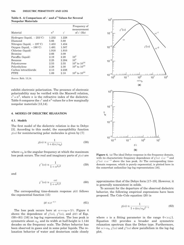
exhibit electronic polarization. The presence of electronicpolarizability may be verified with the Maxwell relation,e1¼n2, where n is the refractive index of the dielectric.Table 8 compares the e1 and n2 values for a few marginallynonpolar materials [13,14].
4. MODELS OF DIELECTRIC RELAXATION
4.1. Models
The first model of the dielectric relation is due to Debye[3]. According to this model, the susceptibility functionw(o) for noninteracting polar molecules is given by [7]
wðoÞ /1
1þ iðo=opÞð58Þ
where op is the angular frequency at which the maximumloss peak occurs. The real and imaginary parts of w(o) are
w0 0ðoÞ /1
1þo2t2ð59Þ
and
w0 0ðoÞ /ot
1þo2t2ð60Þ
The corresponding time-domain response f(t) followsthe exponential function (15)
ft / et=t ð61Þ
The loss peak occurs here at o¼oP¼ 1/t. Figure 4shows the dependence of w0(o), w00(o), and f(t) of Eqs.(59)–(61) [16] in log–log representation. The loss peak issymmetric about op, and its width at half-height is 1.144decades on the frequency scale. The Debye behavior hasbeen observed in gases and in some polar liquids. The re-laxation behavior of water and deuterium oxide closely
approximates that of the Debye form [17–19]. However, itis generally nonexistent in solids.
To account for the departure of the observed dielectricbehavior, the following empirical expressions have beenproposed. The Cole–Cole equation (20) is
wðoÞ /1
1þ ðio=opÞ1a ð62Þ
where a is a fitting parameter in the range 0oar1.Equation (62) provides a broader and symmetricrelaxation spectrum than the Debye type. Furthermore,for o4o0, w0(o) and w00(o) show parallelism in the log–logplot.
Table 8. A Comparison of e0 and n2 Values for SeveralNonpolar Materials
Material n2 e0
Frequency ofmeasurement
of e0 (Hz)
Hydrogen (liquid, 2531C) 1.232 1.228Diamond 5.66 5.68Nitrogen (liquid, 1971C) 1.453 1.454Oxygen (liquid, 1901C) 1.491 1.507Chlorine (liquid) 1.918 1.910Bromine 2.66 3.09Paraffin (liquid) 2.19 2.20 103
Benzene 2.25 2.284 103
Polystryrene 2.53 2.55 102 to 1010
Polyethylene 2.28 2.30 102 to 1010
Carbon tetrachloride 2.13 2.238PTFE 1.89 2.10 102 to 1010
Source: Refs. 13,14.
100
100 100
10−1
10−2
10−3
100
10−1
10−2
10−3
10−4
10−1 101
10010−110−2 101
102
e−t/
−2
−1′′()
′()
/p
t /
(a)
(b)
Figure 4. (a) The ideal Debye response in the frequency domain,with its characteristic frequency dependence of w0(o) po2 andw00(o) po 1 above the loss peak. (b) The corresponding time-domain response, which is purely exponential, is plotted here inthe somewhat unfamiliar log–log representation [16].
946 DIELECTRIC PERMITTIVITY AND LOSS

The Davidson–Cole equation has the form [21]
wðoÞ /1
ð1þ io=opÞb ð63Þ
where b is yet another curve-fitting parameter in therange 0obr1. Equation (63) provides asymmetric relax-ation profiles at oro0, whereas w0(o) and w00(o) remainparallel at o4o0.
The Fuoss–Kirkwood model [22] for the imaginary partof the susceptibility is
w0 0ðoÞ /2ðo=opÞ
g
1þ ðo=opÞ2g ð64Þ
Another relaxation model is given by
wðoÞ /X
1
s¼ 1
GðDsÞ
ðs 1Þ!
expðiDp=2ÞoDoDp
!s
ð65Þ
This is an expansion into the frequency domain ofthe Kolrauch–Williams–Watts function [15] of time:exp[ (t/t)D]. The parameter D in Eq. (65) has no physical
significance and is not based on the physics of dielectricinteractions.
So far the models have had only one fitting parameter,namely, a for the Cole–Cole equation, b for the Davidson–Cole equation, g for the Fuoss–Kirkwood equation, and Dfor the Kolrauch–Williams–Watt equation. The model dueto Havriliak and Negami [23,24], the first one with twoparameters, is given by
wðoÞ /1
½1þ ðio=opÞ1ab
ð66Þ
It should be stressed again that the fitting parameters aand b in this equation have no physical significance.
A classical form of presentation of the dielectric data isto plot w0(o) or e0(o) against w00(o) or e00(o), namely, the so-called Cole–Cole plot [20]. Figure 5 shows the shapes ofthe Debye, Cole–Cole, and Davidson–Cole equations forthe susceptibility functions in Cole–Cole plots. It has beenshown [20] that with the Debye model, a graph of w0(o)against g0(o) over the entire frequency range will be asemicircle and w(N) or eN is obtained from the intercept atthe horizontal axis (see Fig. 5a). Thus the relaxation time tmay be obtained from the slope of a straight line from the
Log ()
Log ()
Log ()
Log ()
Log
Log ( )
−1
(1−) π/2
(0)(0)
0.4
0.2
3 2.1 2.0
1.0
0.30.10.01
0
103101
1030
(ix)1−
0.2 0.4 0.6 0.8 1.0
(0)/2 = m′′(0)/4
0 (0) 00 ∞ (0)
(0)
−2
−1
1− −1
p
p
p = 1/
p = 1/
1/
0
>0
>>0
/2
′′
′′
′
′′
′′
′
′′ ′′
′′/2
′
(a) (b)
(c)
Figure 5. The frequency dependence of thereal and imaginary parts of the susceptibilityand the Cole–Cole presentation for (a) Debye,(b) Cole–Cole, and (c) Davidson–Cole systems [8].
DIELECTRIC PERMITTIVITY AND LOSS 947

origin to a point on the semicircle for which o is known.Now the Cole–Cole relaxation model provides a symmetricbut broader relaxation spectrum, and the correspondingCole–Cole plot is still a semicircle. However, its center isdepressed below the w0 or e0 horizontal axis (see Fig. 5b)with the angle ap/2 between the radius of the circle and w0
or e0 axis. There is no molecular interpretation of this fac-tor a, and it has been interpreted as a ‘‘spreading factor’’ ofthe actual relaxation time about a certain mean value.The magnitude of a must lie between zero and unity. TheCole–Cole plot for the Davidson–Cole model is a skewedplot (see Fig. 5c), representing a severe departure from theDebye relaxation behavior.
The Havriliak–Negami function [23,24] with two pa-rameters, a and b [Eq. (66)], appears to provide the bestresults for the fitting of the measured dielectric data formost materials. However, none of these mathematicalmodels that invoke a distribution of relaxation energies(25) or times offer any physical interpretation of materialproperties [26–29] .
It has been suggested that a dielectric loss spectrummay be regarded as a mathematical summation of a dis-tribution function g(t) of Debye responses correspondingto a distribution of relaxation times [30]; thus
wðoÞ¼Z 1
0
gðtÞ1þ ior
dt ð67Þ
The distribution functions are always positive, andcurves of w00(o) or e00(o) can be formed from them by thesuperposition of many single relaxation-time or frequencycurves [31]. It has been shown [32] that the product of theelapsed time and the depolarization current is a convolu-tion of the distribution function of relaxation frequencieswith a weight function of an asymmetric bell shape. Asimilar relationship is also shown to exist for the imagi-nary part of the permittivity. The same work [32] alsoproposes a deconvolution procedure to determine the dis-tribution function of relaxation frequencies from experi-mental data. A distribution of relaxation times from thefrequency dependence of the real part of the complex per-mittivity has also been made with the inverse Fouriertransformation [33]. As stated earlier, however, no distri-bution of relaxation times that can claim physical realitycan be associated with relaxation systems in condensedmatter [8,26,27].
A two-parameter model for the complex susceptibilityfunction w(o), known as the universal relaxation law, hasbeen proposed [8,16], which states that all solid dielectricsfollow fractional power laws in frequency. It is of interestto note that w(o) may be expressed by a simple empiricalexpression [16,23]
wðoÞ¼A½1þ ðixÞmðn1Þ=m ð68Þ
where the exponents m and n lie between zero and unityand x is the normalized frequency. Equation (68) indicatesthat the experimental state of dielectric susceptibility canbe fitted with two power-law exponents. The Debye func-tion is a limiting form of this equation for m¼ 1 and n¼ 0.
For the symmetric loss peak at op and x¼ 1, we havem¼ 1n. Furthermore, the ratio w00(o)/w0(o) decreases asm and 1n become smaller, thus providing broader peaksas in the case of the Cole–Cole function. This leads to theuniversal law, characterized by two fractional power lawsin frequency respectively below and above the loss peakfrequency oP [8,16]
w0 0ðoÞ¼ tanmp2
½wð0Þ w0ðoÞ / om for oop ð69Þ
for oop and
w0 0ðoÞ¼ cotnp2
w0ðoÞ / on1 for ocop ð70Þ
where the exponents are in the ranges 0ono1 and0omo1.
As a result, in the high-frequency range of the losspeak, the ratio of the imaginary to the real part of thecomplex susceptibility is a frequency-independent con-stant:
w0 0ðoÞw0ðoÞ
¼ cotnp2
ð71Þ
Hence, in a log–log plot w00(o) and w0(o) appear as par-allel lines for ocop. It should be noted that for the Debyeprocess this ratio is ot and thus increases linearly withfrequency, which is consistent with the idea that the pro-cess is a ‘‘viscous’’ phenomenon in which the dielectric lossis linearly related to the angular velocity [16].
For the low-frequency part of the loss peak (ooop), wehave [8,15]
w0 0ðoÞDw0ðoÞ
¼ tanmp2
ð72Þ
where Dw0(o)¼ w(0)w0(o) is known as the dielectric de-crement and is the extent to which the polarization at anyparticular frequency falls short of the value of the equi-librium polarization in a static field. Equations (69) and(70) may be represented by the empirical law combiningthe two fractional power laws above and below op [8]:
w0 0ðoÞ /1
ðo=opÞmþðo=opÞ
1nð73Þ
The Fourier transforms of fractional power laws corre-late the frequency-domain dielectric parameters withtheir time-domain behavior thus (16):
om / tm1 for tct ð74Þ
on1 / tn for tt ð75Þ
In the carrier-dominated low-frequency dispersion(LFD) or quasi-DC (QDC) systems, mobile charge carri-ers, such as ions and electrons, act as polarizing speciesand provide a broad dielectric response [16,34–36]in which no loss peak is observed. The LFD (or QDC)
948 DIELECTRIC PERMITTIVITY AND LOSS

relaxation is characterized by two independent processes,below and above a certain critical frequency oc, which maybe represented by Eq. (70). The real and imaginary partsof the complex dielectric susceptibility steadily increasewith decreasing frequency for small values of n2, at fre-quencies less than oc. This is followed by a flat loss be-havior above oc with n1E1 [8,16,28]. The frequency oc
plays a role analogous to that for op in a dipolar system.Figure 6 shows [16] typical behavior of w(o) for the LFD
(or QDC) system. Figure 7 shows schematically the typicaltime-domain behavior of a dipolar LFD (or QDC) systemtogether with the flat loss response corresponding to n-1[15]. Note that the flat loss behavior is the limiting case ofthe dielectric response that occurs in low-loss materialswith a very small value of the ratio w00(o)/w0(o). The value
of n2 can never be zero, and hence n cannot actually have avalue of 1, although nearly flat loss behavior has been ob-served experimentally.
There are few examples of solids, including single crys-tals of ferroelectrics, that show pure Debye relaxation be-havior. A variety of solids (viz., low-loss dielectrics, dipolarmaterials, semiconductor p-n junctions, and biological ma-terials) are known to show dielectric dispersions that maybe fitted with the universal fractional power law [Eq. (73)].Furthermore, dipolar systems exhibit loss peaks, whereasthe carrier-dominated systems exhibit LFD (or QDC)behavior [8,34,35].
A stochastic model for the universal dielectric disper-sion has also been proposed [37–39]. This probabilisticmodel is based on the assumption that individual dipolesand their environments interact during the process ofrelaxation and the dielectric response function is givenby [37]
fðtÞ¼f0aopðoptÞa1½1þ kðoptÞa ð76Þ
where f0 is a constant of the relaxation function f(t), andk is a positive real number. In the short-time limit thisfunction is
fðtÞ ðoptÞa1¼ ðoptÞn
ð77Þ
where n¼ 1 a and 0ono1. The corresponding long-timelimit is
fðtÞ ðoptÞðaþ kÞ=k¼ ðoptÞm1
ð78Þ
where m¼ a/k and 0omo1 if aok. The exponents mand n of the universal fractional law [8] are thus relatedby [37]
m¼1 n
kð79Þ
where k41n and 0ono1. If 1nokr1, then1nrmo1, and this is observed in most analyzed exper-imental results. For k¼ 1 we have m¼ 1n, and this isthe Cole–Cole response. For k¼ 1n we have m¼ 1,which is the Davidson–Cole response. If k41, then0omo1, which is observed only in a small number ofanalyzed data [21,33,38]. In this case, k-0 and theWilliams–Watts response is observed [15,40]. Theprobabilistic model [37–39] thus suggests a relationbetween the empirical parameters m and n, defining thelow- and high-frequency regions of the complex dielectricsusceptibility. It has been suggested [37] that the param-eter (k) may be related to the waiting-time distribution ofthe relaxing dipoles, which may follow a Weibull distribu-tion, namely
RðsÞ ¼ expðksdÞ ð80Þ
where R(s) is the waiting-time distribution, k is a positivereal number, and 0odo1. It has been shown [37] that fora particular waiting-time distribution function, the
10−5
10−1
10−4 10−3 10−2 10−1 100
100
101
102
103
104
105
′′()
′()
(s−1)
101 102 103 104 105
Figure 6. The frequency dependence of a system dominated byLFD or QDC with n1¼0.8 at high frequencies and n2¼0.5 at lowfrequencies. The crossover point is deliberately shifted to highfrequencies to show the LFD or QDC region [16].
10−3 10−2 10−1 100 101 10210−1
100
101
102
103
104
105
103
x
x−1.6
x −0.2
x −0.8
′ ()
′ ()
(Dipolar)
LFDcharge carriers
f(x
)
e(−)
Debye
x −1
(flat loss)
Figure 7. The time-domain response f(t/t) of typical dielectricsystems, including the Debye exponential response; the dipolarresponse with n¼0.8, m¼0.6; the carrier-dominated LFD re-sponse with n1¼0.8, n2¼0.2; and the flat loss with n¼1 [16].
DIELECTRIC PERMITTIVITY AND LOSS 949
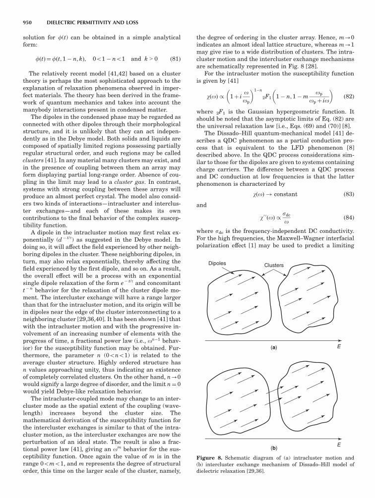
solution for f(t) can be obtained in a simple analyticalform:
fðtÞ¼fðt; 1 n; kÞ; 0o1 no1 and k > 0 ð81Þ
The relatively recent model [41,42] based on a clustertheory is perhaps the most sophisticated approach to theexplanation of relaxation phenomena observed in imper-fect materials. The theory has been derived in the frame-work of quantum mechanics and takes into account themanybody interactions present in condensed matter.
The dipoles in the condensed phase may be regarded asconnected with other dipoles through their morphologicalstructure, and it is unlikely that they can act indepen-dently as in the Debye model. Both solids and liquids arecomposed of spatially limited regions possessing partiallyregular structural order, and such regions may be calledclusters [41]. In any material many clusters may exist, andin the presence of coupling between them an array mayform displaying partial long-range order. Absence of cou-pling in the limit may lead to a cluster gas. In contrast,systems with strong coupling between these arrays willproduce an almost perfect crystal. The model also consid-ers two kinds of interactions—intracluster and interclus-ter exchanges—and each of these makes its owncontributions to the final behavior of the complex suscep-tibility function.
A dipole in the intracluster motion may first relax ex-ponentially (d t/t) as suggested in the Debye model. Indoing so, it will affect the field experienced by other neigh-boring dipoles in the cluster. These neighboring dipoles, inturn, may also relax exponentially, thereby affecting thefield experienced by the first dipole, and so on. As a result,the overall effect will be a process with an exponentialsingle dipole relaxation of the form e t/t and concomitanttn behavior for the relaxation of the cluster dipole mo-ment. The intercluster exchange will have a range largerthan that for the intracluster motion, and its origin will bein dipoles near the edge of the cluster interconnecting to aneighboring cluster [29,36,40]. It has been shown [41] thatwith the intracluster motion and with the progressive in-volvement of an increasing number of elements with theprogress of time, a fractional power law (i.e., on1 behav-ior) for the susceptibility function may be obtained. Fur-thermore, the parameter n (0ono1) is related to theaverage cluster structure. Highly ordered structure hasn values approaching unity, thus indicating an existenceof completely correlated clusters. On the other hand, n-0would signify a large degree of disorder, and the limit n¼ 0would yield Debye-like relaxation behavior.
The intracluster-coupled mode may change to an inter-cluster mode as the spatial extent of the coupling (wave-length) increases beyond the cluster size. Themathematical derivation of the susceptibility function forthe intercluster exchanges is similar to that of the intra-cluster motion, as the intercluster exchanges are now theperturbation of an ideal state. The result is also a frac-tional power law [41], giving an om behavior for the sus-ceptibility function. Once again the value of m is in therange 0omo1, and m represents the degree of structuralorder, this time on the larger scale of the cluster, namely,
the degree of ordering in the cluster array. Hence, m-0indicates an almost ideal lattice structure, whereas m-1may give rise to a wide distribution of clusters. The intra-cluster motion and the intercluster exchange mechanismsare schematically represented in Fig. 8 [28].
For the intracluster motion the susceptibility functionis given by [41]
wðoÞ / 1þ ioop
1n
2F1 1 n; 1mop
opþ io
ð82Þ
where 2F1 is the Gaussian hypergeometric function. Itshould be noted that the asymptotic limits of Eq. (82) arethe universal relaxation law [i.e., Eqs. (69) and (70)] [8].
The Dissado–Hill quantum-mechanical model [41] de-scribes a QDC phenomenon as a partial conduction pro-cess that is equivalent to the LFD phenomenon [8]described above. In the QDC process considerations sim-ilar to those for the dipoles are given to systems containingcharge carriers. The difference between a QDC processand DC conduction at low frequencies is that the latterphenomenon is characterized by
wðoÞ ! constant ð83Þ
and
w0 0ðoÞ /sdc
oð84Þ
where sdc is the frequency-independent DC conductivity.For the high frequencies, the Maxwell–Wagner interfacialpolarization effect [1] may be used to predict a limiting
E(a)
(b)
Dipoles Clusters
E
Figure 8. Schematic diagram of (a) intracluster motion and(b) intercluster exchange mechanism of Dissado–Hill model ofdielectric relaxation [29,36].
950 DIELECTRIC PERMITTIVITY AND LOSS
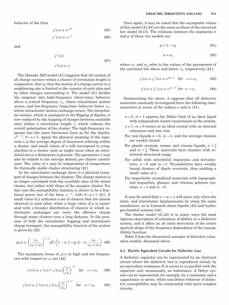
behavior of the form
w0ðoÞ / o2 ð85Þ
w0 0ðoÞ / o1 ð86Þ
and
w0 0ðoÞ
w0ðoÞ / oð87Þ
The Dissado–Hill model [41] suggests that the motion ofall charge carriers within a cluster of correlation length iscooperative, that is, that the motion of a charge carrier to aneighboring site is limited to the vacancy of such sites andby other charges surrounding it. The model [41] dividesthe response into high-frequency (short-time) behaviorabove a critical frequency oc, where intracluster motionoccurs, and low-frequency (long-time) behavior below oc,where intracluster motion exchange occurs. The intraclus-ter motion, which is analogous to the flipping of dipoles, isnow replaced by the hopping of charges between availablesites within a correlation length x, which reduces theoverall polarization of the cluster. The high-frequency re-sponse has the same functional form as for the dipoles:on1, 0ono1. Again the physical meaning of the expo-nent n is the average degree of structural ordering withina cluster, and small values of n will correspond to irreg-ularities in a cluster such as might occur when an inter-stitial ion or a dislocation is present. The parameter n mayalso be related to the entropy density per cluster constit-uent. The value of n may be independent of temperaturefor thermally stable cluster structuring [41].
In the intercluster exchange there is a physical trans-port of charges between the clusters. The charge motion isno longer correlated with the available sites of the donorcluster, but rather with those of the acceptor cluster. Forthis case the susceptibility function is shown to be a frac-tional power law of the form op, with 0opo1 [41]. Asmall value of p indicates a set of clusters that are almostidentical to each other, while a large value of p is associ-ated with a broader distribution of clusters in which in-tercluster exchanges can carry the effective chargethrough many clusters over a long distance. In the pres-ence of both the intracluster hopping and interclustercharge transport, the susceptibility function of the systemis given by [42]
wðoÞ /oc
ocþ io
1n
2F1 1 n;1þp;2 n;oc
ocþ io
ð88Þ
The asymptotic forms of w(o) at high and low frequen-cies with respect to oc are [42]
w0ðoÞ / w0 0ðoÞ w0ðocÞooc
p
for ooc ð89Þ
w0ðoÞ / w0 0ðoÞ / w0ðocÞooc
n1
for o > oc ð90Þ
Once again, it may be noted that the asymptotic valuesof this model [41,42] are the same as those of the universallaw model [8,15]. The relations between the exponents nand p of these two models are
p¼1 n2 ð91Þ
n¼n1 ð92Þ
where n1 and n2 refer to the values of the parameters ofthe universal law above and below oc, respectively [41]:
w0ðoÞ / w0 0ðoÞ / on21 for ooc ð93Þ
w0ðoÞ / w0 0ðoÞ / on11 for o > oc ð94Þ
Summarizing the above, it appears that all dielectricmaterials commonly investigated have the following char-acteristics in terms of the indices n and m (41):
n¼ 0, m¼1 express the Debye limit of an ideal liquidwith independent cluster constituents in the system.
n¼ 1, m¼ 0 occurs in an ideal crystal with no internalrelaxation and zero loss.
For real liquids n-0, m-1, and the average clustersare weakly bound.
For plastic crystals, waxes, and viscous liquids, n 12
and m 12. These materials have clusters with re-
stricted structural range.
For solids with interstitial impurities and ferroelec-trics, n-0 and m-1. Ferroelectrics have weaklybound clusters of dipole reversals, thus yielding asmall value of n.
For imperfectly crystallized materials with topograph-ical impurities, glasses, and vitreous polymer sys-tems, n-1 and m-0.
It may be noted that nþm¼ 1 will occur only when theintra- and intercluster displacements lie along the samecoordinates, as in Lennard–Jones liquids [43] and hydro-gen-bonded systems [44].
The cluster model [41,42] is in many ways the mostrigorous description of relaxation of defects in a dielectricsystem, and it offers an ab initio derivation of the entirespectral shape of the frequency dependence of the suscep-tibility function.
Table 9 lists the theoretical concepts of dielectric relax-ation models, discussed above.
4.2. Electric Equivalent Circuits for Dielectric Loss
A dielectric capacitor can be represented by an electricalcircuit where the dielectric loss is reproduced mainly byan equivalent resistance R in series or in parallel with thecapacitor and, occasionally, an inductance. A Debye sys-tem can be represented, for example, by a resistance and acapacitance in series, while non-Debye behavior of dielec-tric susceptibility may be constructed with more complexcircuits.
DIELECTRIC PERMITTIVITY AND LOSS 951
For such cases, the concept of a universal capacitor [8]has been proposed, and the resulting frequency depen-dence of the dielectric parameters is
wðoÞ / CnðoÞ¼ bðioÞn1¼ b sin
np2 i cos
np2
on1 ð95Þ
It should be noted that for nonideal dielectric responses,the circuit elements will have frequency-dependentdispersive properties. Figure 9 shows schematic represen-tations of simple circuit combinations of ideal, frequency-independent elements and some forms of presentation ofdielectric data. The frequency response of lossy capacitorsof the type represented by Eq. (89) is shown in Fig. 10[8,36,45]. The association of universal capacitors and dis-persive circuit elements is schematically represented inTable 10 [29].
4.3. Relaxation Behavior in Materials
The relaxation phenomena have been studied for a widerange of materials, from covalent, ionic, and van der Waalscrystals at one extreme through glasses, liquids contain-ing suspensions, solid synthetic polymers, and p-n junc-tions at the other [41].
The permittivity of nonpolar gases at normal pressureis close to unity, and the Clausius–Mossotti equation [23]
adequately describes its variation with moderate densitychanges [46]. At high pressures the molar polarization ofgases deviates from the Clausius–Mossotti equation. Themolecular polarizability is enhanced by the attractive forc-es between the molecules, whereas the repulsive forcesdecrease it.
Centrosymmetric molecules do not possess dipoleor octupole moments, but quadrupole moments maybe present in some gases, such as hydrogen, carbondioxide, carbon disulfide, oxygen, nitrogen, benzene, andethylene. Tetrahedral molecules, on the other hand,have zero dipole and quadrupole moments (e.g., methaneand carbon tetrachloride) [46]. The presence of higherdipole moments in a molecule induces moments on itsneighbors and produces deviations from the Clausius–Mossotti equation. Polar gases display temperature de-pendence of the orientational polarization, and theirdielectric loss spectra follow the Debye relaxation behav-ior in which partial orientation of the permanent dipolesoccurs under an externally applied field. Polar gasesabsorb energy in the microwave region through two pro-cesses: rotational absorption and unquantized molecularcollision. The high-frequency dielectric properties of gaseshave been well reviewed [47,48] and will not be discussedfurther here.
There is as yet no exact theory of liquids, which havebeen treated either as dense gases or as disordered solids.
Table 9. Theoretical Concepts of Relaxation Models
Function Equation Parameters
Debyew0 0ðoÞ /
1
ðo=opÞ1þðo=opÞ
(26) a¼0 b¼1
Cole–Colew0 0ðoÞ /
1
ðo=opÞa1þðo=opÞ
1a
(27) 0oao1 b¼1
Davidson–Colew0 0ðoÞ /
1
ðo=opÞ1þðo=opÞ
b
(28) a¼0 0obo1
Havriliak–Negamiw0 0ðoÞ /
1
ðo=opÞa1þðo=opÞ
bð1aÞ
(29) 0oao1, 0obo1
Jonscher, Dissado, and Hill (dipolar peak)w0 0ðoÞ /
1
ðo=opÞmþðo=opÞ
n1
(21) 0omo1 0ono1
Jonscher, Dissado, and Hill (QDC process) w0ðoÞ / w0 0ðoÞ / on21 for ooc(24) 0on2o1 0on1o1
w0ðoÞ / w0 0ðoÞ / on21 for ococ(25)
Weron (stochastic model) fðtÞ¼f0aopðoptÞa1½1þkðoptÞað1þkÞ=k (41) m¼ (1n)/k 1nomo1
Source: Refs. 29,36.
952 DIELECTRIC PERMITTIVITY AND LOSS

The dielectric relaxation in polar liquids (dilute solutions)with spherical dipolar molecules can be interpreted interms of the orientation of individual dipoles. In the Debyeprocess, it is assumed that a spherical dipolar moleculeobeys Stokes’ law, which states that the relaxation time isproportional to the shear viscosity of the liquid and to r3,where r is the radius of the sphere. However, the relax-
ation time must depend on the viscosities of both the sol-vent and the solute. The molecular radius calculated fromthe relaxation time with the Debye model is usually toosmall. Improved fit to the relaxation behavior of liquidsmay be obtained with empirical formulas (Cole–Cole [20],Davidson–Cole [21], Havriliak–Negami [23,24]) and theuniversal law [8].
Circuit Z Y C () comments
Resonance
Debye
L R
R 1/R
1/R
1/R
R
R
RR
C
C
C
C
C
C
C
C1 C2
C0
C0< Cs
C∞C∞
1
1
′
′
2 2
∞
∞
Cs
C
G
G
G1/G
1/G
1/G
G
G0
G1
G1 G2
Gb
"Leaky"capacitor
Seriesbarrier
Diffusion
Effect ofnonzero 0
/4
o
o
o
o
0
0
σ0
′′ ′′
′′ ′′
′
′1 2
12 2
12
1
2
12
22
122 1
>>
C
C+C∞
Cs
(a)
(b)
(c)
(d)
(e)
(f)
(g)
(h)
(i)
(j)
Figure 9. Schematic representation of simple circuitsformed as a combination of ideal, frequency-indepen-dent elements (a–h) and some forms of presentation ofdielectric data (i, j) [8,36,45].
DIELECTRIC PERMITTIVITY AND LOSS 953
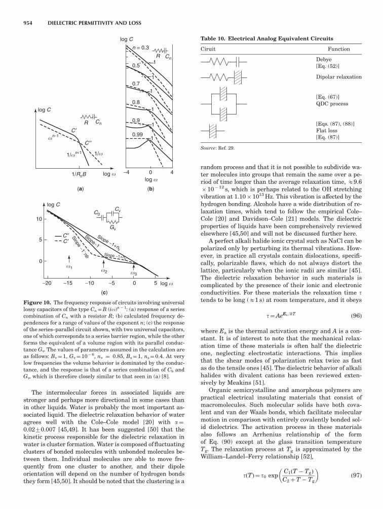
The intermolecular forces in associated liquids arestronger and perhaps more directional in some cases thanin other liquids. Water is probably the most important as-sociated liquid. The dielectric relaxation behavior of wateragrees well with the Cole–Cole model [20] with a¼0.0270.007 [45,49]. It has been suggested [50] that thekinetic process responsible for the dielectric relaxation inwater is cluster formation. Water is composed of fluctuatingclusters of bonded molecules with unbonded molecules be-tween them. Individual molecules are able to move fre-quently from one cluster to another, and their dipoleorientation will depend on the number of hydrogen bondsthey form [45,50]. It should be noted that the clustering is a
random process and that it is not possible to subdivide wa-ter molecules into groups that remain the same over a pe-riod of time longer than the average relaxation time, E9.6 1012 s, which is perhaps related to the OH stretchingvibration at 1.10 1013 Hz. This vibration is affected by thehydrogen bonding. Alcohols have a wide distribution of re-laxation times, which tend to follow the empirical Cole–Cole [20] and Davidson–Cole [21] models. The dielectricproperties of liquids have been comprehensively reviewedelsewhere [45,50] and will not be discussed further here.
A perfect alkali halide ionic crystal such as NaCl can bepolarized only by perturbing its thermal vibrations. How-ever, in practice all crystals contain dislocations, specifi-cally, polarizable flaws, which do not always distort thelattice, particularly when the ionic radii are similar [45].The dielectric relaxation behavior in such materials iscomplicated by the presence of their ionic and electronicconductivities. For these materials the relaxation time ttends to be long (E1 s) at room temperature, and it obeys
t¼AeEa=kT ð96Þ
where Ea is the thermal activation energy and A is a con-stant. It is of interest to note that the mechanical relax-ation time of these materials is often half the dielectricone, neglecting electrostatic interactions. This impliesthat the shear modes of polarization relax twice as fastas do the tensile ones [45]. The dielectric behavior of alkalihalides with divalent cations has been reviewed exten-sively by Meakins [51].
Organic semicrystalline and amorphous polymers arepractical electrical insulating materials that consist ofmacromolecules. Such molecular solids have both cova-lent and van der Waals bonds, which facilitate molecularmotion in comparison with entirely covalently bonded sol-id dielectrics. The activation process in these materialsalso follows an Arrhenius relationship of the formof Eq. (90) except at the glass transition temperatureTg. The relaxation process at Tg is approximated by theWilliam–Landel–Ferry relationship [52],
tðTÞ¼ t0 expC1ðT TgÞ
C2þT Tg
ð97Þ
log
1/
n−1
1/n+1
log
log
1 2 3
Cv
Gv
C0
Cn
Cn
C′′
C ′
C ′′
C ′
log C
log C
log C
R
R
1/RoB
10
5
0
0
0
−20 −15 −10 −5
−4 4
5
Slope−1
Slope −1 −nb
Slope −1+nb
Slope −1+ny
n = 0.3
0.5
0.7
0.8
0.9
0.99
1
1
1
1
1
1
(b)(a)
(c)
Figure 10. The frequency response of circuits involving universallossy capacitors of the type Cn¼B (io)n 1: (a) response of a seriescombination of Cn with a resistor R; (b) calculated frequency de-pendences for a range of values of the exponent n; (c) the responseof the series–parallel circuit shown, with two universal capacitors,one of which corresponds to a series barrier region, while the otherforms the equivalent of a volume region with its parallel conduc-tance Gv. The values of parameters assumed in the calculation areas follows: Bv¼1, Gv¼10 6, nv ¼ 0.85, Bs¼1, ns¼0.4. At verylow frequencies the volume behavior is dominated by the conduc-tance, and the response is that of a series combination of Cb andGv, which is therefore closely similar to that seen in (a) [8].
Table 10. Electrical Analog Equivalent Circuits
Ciruit Function
Debye[Eq. (52)]
Dipolar relaxation
[Eq. (67)]QDC process
[Eqs. (87), (88)]Flat loss[Eq. (87)]
Source: Ref. 29.
954 DIELECTRIC PERMITTIVITY AND LOSS

where t0 is a constant, and C1 and C2 are also constantswith values E17 and E51, respectively [46]. The relax-ation time t decreases with increasing temperature, asmay be observed in isochronal plots of depolarizing cur-rent against temperature [53].
The relaxation behavior of polymers is related to sev-eral complex physical parameters—shear modulus, heatcapacity, permittivity, and refractive index—which exhibittransitions with increasing temperature [54] (see Fig. 11).In an amorphous polymer the principal transition is theglass transition at a temperature Tg, which is labeled asthe a transition at Ta in Fig. 11. Above Tg the free volumedecreases to a critical value, thus severely restricting thesegmental motions of the polymer chains. In a semicrys-talline polymer there will be an additional transitionalphenomenon at the melting temperature Tm. There areother secondary transitions, b and g in order of decreasingtemperature (i.e., Ta4Tb4Tg). For example, in polyeth-ylene, the a, b, and g relaxations at 1 kHz occur at 77, 13,and 1131C, respectively. The a relaxation is attributed tomotions in the crystalline phase, and the b relaxationarises from primary motions of the chain branches in theamorphous phase. The g relaxation may be associated witha combination of processes including defect migration andthe reorientation motion in the amorphous phase [55]. Thea, b, and g relaxations in polypropylene occur at 80, 0, and 801C. Table 11 gives the glass transition temperaturesTg of some common polymers [54].
4.4. Experimental Evidence of Frequency Response and aComparison with the Cluster Models
Although ideal Debye response in ferroelectric single crys-tals has been observed [56], there exist, in general, veryfew examples of such responses in condensed matter. Al-though water may be regarded as a classic dielectric, itsdielectric behavior displays a broadened relaxation peakthat departs from a true Debye relation [8,57]. Near-Debye relaxation responses have also been observed insilicon p-n junctions [8]. It may not be appropriate to
discuss experimentally observed dielectric dispersion datawith the Cole–Cole, Davidson–Cole, and Havriliak–Negami models, which are basically empirical in nature.However, relaxation spectroscopy can provide consider-able information on dielectric materials from the mea-surement of the shape of the loss peak as well as therelaxation rate and amplitude. The shape of a loss peak isclearly characterized by the parameters m and n of theDissado–Hill [41,42] and universal law [8] models. Thisprocedure has been employed to demonstrate the presenceof cluster structure in (1) the viscous liquid produced fromthe glassy state above a glass transition [58], (2) plasticcrystal phases [59], and (3) ferroelectrics [60,61]. The clus-ter size becomes strongly temperature-dependent in fer-roelectrics near the Curie temperature [61]. Theamplitude and the relaxation rate are related [60–62].These considerations also hold true for liquid crystals[60,61,63]. Figures 12a and 12b show the observed dielec-tric response of poly-r-benzyl-L-glutamate (PBLG) andpoly-r-methyl-L-glutamate (PMLG), respectively [42].The loss peaks in both cases are broad with values of nand m in conformity with the cluster model [41]. Table 12gives the values of shape indices n and m for PBLG indifferent states, from which it may be observed that as thelocal order decreases in solution, the value of n decreases,and that of m increases [41,63]. These examples coversome typical cluster structures with different values of mand n [41].
It is suggested that the quantum-mechanical clustermodel provides explanations for the relaxation dynamicsin materials that show non-Debye susceptibility behaviorover a wide frequency range. The cluster model shows thatthe free energy of a cluster is held constant and its entropy
TγTγTγ
Temperature
P
Q
Phy
sica
l qua
ntity
Figure 11. Schematic diagram of the temperature dependence ofcomplex properties of polymers [54].
Table 11. Glass Transmission Temperature Tg ofCommon Polymersa
Polymer Tg (1C)
PE 90, 35PP 10Polymethylpentene 30PS 95PAN 105PVC 85PVF 20, 45PVDC 15PA 6 50PA 66 90PA 610 40PMMA 105POM 90, 10Poly(phenylene oxide) 210PC 150PETP 65CA 105NR 75CR 45NBR 20
Source: Ref. 54.aThese are approximate values; where two temperatures are given, the
assignment of the glass transition remains doubtful. Tm is independent of
chain length for high-molar-mass polymers, but falls somewhat as the
chains become very short.
DIELECTRIC PERMITTIVITY AND LOSS 955

evolves at the expense of its internal energy (i.e., en-thalpy), resulting in a power-law relaxation process.
5. APPLICATION OF DIELECTRIC SPECTROSCOPY INDETECTING AGING IN INSULATING POLYMERS
5.1. Dielectric Aging and Treeing
Polymers experience aging when subjected to a mechan-ical or electric stress over an extended period of time. Theaging produces irreversible deterioration of physical,chemical, and dielectric and other electrical properties,which may eventually lead to electrical breakdown of an
insulating polymer. It must be stressed that physical andchemical aging may occur independently without the ap-plication of an external electric field. However, the agingprocess may be accelerated by the field in conjunction withother factors.
The mechanisms for electrical breakdown have beenextensively reviewed [64]. The chemical aging modelshave also been reviewed [65] and will not be discussed indetail here. The present section provides in brief the re-sults of a study of aging of polyethylene under an AC fieldin humid environment by dielectric spectroscopy.
Dielectric aging in a dry environment at moderate tohigh electric field appears to begin mostly at imperfectionsin materials where the local field tends to be enhanced. Atsuch locations, treelike electrical channels may form andpropagate due to the occurrence of partial discharges.Space charges play a significant role in the initiationand growth of electrical trees [66]. Water trees in poly-meric insulators with AC fields in humid environmentsmay arise from microphase separation in partially oxi-dized polymers as a result of field-induced electrochemicalprocesses [67]. It has been shown that water trees in cross-linked polyethylene consist of tracks of hydrophiliccarboxylate salts in the amorphous phase of the polymer[68–70]. The dielectric aging and the water tree growthincorporate electrochemical processes following the elect-rophysical process of water and ion diffusion in the poly-mer [68]. It has been suggested that the electrochemicaldegradation of polyolefins associated with aging and watertreeing involve five fundamental steps: (1) electrolysis ofwater, in which oxygen and hydrogen peroxide radicalsare formed, as both are oxidizing agents; (2) initiation ofdegradation; (3) catalysis of degradation by metal ions; (4)chain scission, resulting in the formation of ketones andcarboxylate ions; and (5) conversion of ketones to carboxy-late ions [71]. Electric-field-driven oxidation has also beenproposed by other workers [64,72–74].
The electrooxidation occurs in the local field direction,and water tree tracks are formed by chain scission in theamorphous regions of the polymer. The track region is hy-drophilic. As a result, water molecules in the polymer ma-trix condense to form liquid water in the track, which thentransports ions to provide further oxidation at the tip ofthe track. Thus a track propagates itself in a similar man-ner to that of a self-propagating electrical tree or a gasbreakdown channel, although at a different rate [71].
It may thus be expected that aging and its progress dueto the electrooxidation of a polymer in a humid environ-ment may be detected by a study of its dielectric behaviorover a wide frequency range.
5.2. Evidence of Aging in Frequency Response
Figure 13 shows the frequency response of the real andthe imaginary parts [w0(o) and w00(o), respectively] of thecomplex susceptibility w(o) of unaged and crosslinkedpolyethylene (XLPE) cable samples and samples AC-aged (6 kV/mm, 50 Hz) for up to 6000 h in water at roomtemperature [36,75]. It may be observed from the fittedresponse that there are three relaxation processes: (1) ahigh-frequency (HF) loss peak at B5 105 Hz, (2) a
105
10−1
10−2
1
1
10
10910Frequency (Hz)
105 10910Frequency (Hz)
(
)
10−1
10−2
10
(
)
333 323 315 308 296 K
299 275 257246 229 K
(a)
(b)
Figure 12. Master curves for the dielectric response of orientedfilms of (a) PBLG and (b) PMLG. The theoretical spectral shape inthe plots has been determined with the values (a) m¼0.28,n¼0.87; (b) m¼0.24, n¼0.92. Plot (a) is scaled at 333 K; (b), at299 K. In both, the small magnitude of the dispersion has limitedthe accuracy with which the real part of the susceptibility couldbe determined for the higher frequency values [42].
Table 12. Spectral Shape Indices Observed in DielectricResponse of PBLG in Different Physical States
Sample m n
Solid, orientationally ordered film 0.28 0.87Solid, prepared by the Leuch method 0.42 0.81Solution in benzene with e-caprolactam 0.78 0.50Solution in trans-1,2-dichloroethylene
containing NN-formidemethylamide1.0 0.50
Solution in purified ethylene dichloride 0.78 0.49Solution in ethylene dichloride 0.61 0.49Solution in dioxan — 0.44Solution in dioxan with DMF 0.76 0.51Solution in dioxan 0.81 0.54
Source: Refs. 41,63.
956 DIELECTRIC PERMITTIVITY AND LOSS
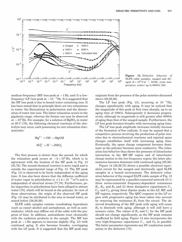
medium-frequency (MF) loss peak at B1 Hz, and (3) a low-frequency (LF) loss peak at B104 Hz. It is suggested thatthe HF loss peak is due to bound water containing ions. Ithas been stated that in principle there are two relaxationsin water: the fluctuations in polarization and the dissoci-ation of water into ions. The latter relaxation occurs in thegigahertz range, whereas the former one may be observedat B105 Hz. For example, for a solution of MgSO4 in waterat 201C [76], the following chemical reactions of the elec-trolyte may occur, each possessing its own relaxation char-acteristic:
Mg2þþOHÐMgOH
SO24 þHþÐHSO4
The first process is slower than the second, for whichthe relaxation peak occurs at B2 105 Hz, which is inagreement with the location of the HF peak in Fig. 13[45,76]. The second chemical reaction is more rapid and isoutside the experimental range of Fig. 13. The HF peak(Fig. 13) is observed to be fairly independent of the agingtime. It has also been shown that the diffusion coefficientof water vapor in polyethylene is E1.4 106 m2/s and isindependent of electrical stress [77,78]. Furthermore, po-lar impurities in polyethylene have been alleged to attractwater [70], which will be bound in the polymer. In view ofthese observations, the origin of the observed HF peak(Fig. 13) may be attributed to the ions in bound water, asstated before [28,29,36].
XLPE cable samples contain crosslinking byproducts(such as cumyl alcohol and acetophenon, as well as anti-oxidants), which may diffuse out of the cable with the pro-gress of time. In addition, antioxidants react chemicallywith the oxidation products in the sample. The MF losspeak at B1 Hz appears to increase slightly (Fig. 13) withcontinued aging. It also becomes broader, overlappingwith the LF peak. It is suggested that the MF peak may
originate from the presence of the polar moieties discussedabove [28,29,36].
The LF loss peak (Fig. 13), occurring at 10 4 Hz,changes significantly with aging. It may be noticed thatthe magnitude of this peak at first rises sharply, up to anaging time of 1000 h. Subsequently it decreases progres-sively, although its magnitude is still greater after 6000 hof aging than that of the unaged sample. Furthermore, theLF loss peak becomes broader with increasing aging time.
The LF loss peak amplitude increases initially becauseof the formation of free radicals. It may be argued that acompetitive process involving the production of polar moi-eties due to electrochemical reactions and injected spacecharges establishes itself with increasing aging time.Eventually, the space charge component becomes domi-nant as the polymer becomes more conductive. The relax-ation loss behavior thus shows the presence of intraclusterinteraction in the MF–HF region and of interclustercharge motion in the low-frequency region; the latter phe-nomenon becomes dominant with continued aging [29,36].
Figure 14 [28,36,75] shows a possible electrical equiv-alent circuit for the unaged and electrically aged XLPEsamples in a humid environment. The dielectric relax-ation behavior of the unaged XLPE cable sample of Fig. 13may be represented by a parallel-connected network of (1)three series-connected frequency-dependent resistancesR1, R2, and R3 and (2) three dissipative capacitances C1,C2, and C3, giving three dipolar peaks in the LF, MF, andHF regions, respectively. The QDC response in the LF re-gion with progressive aging has been taken into accountby removing the resistance R3 from the circuit. The ob-served broadening of the MF peak with aging will causeR2 to diminish with aging, although it will still have anonzero value. The values of R1 and C1 for the HF peakshould not change significantly, as the HF peak remainsunaffected by field aging. Figure 14 also incorporates thevery high-frequency capacitance CN and G0 in parallel.The latter parameter represents any DC conduction mech-anism in the dielectric [75].
10−1
10−2
10−3
10−4
100
10−6 10−410−5 10−3 10−2 10−1 100 101 102 103 104 105 106
Frequency (Hz)
′,χ
′′ Unaged
1000 h
2000 h
4000 h
6000 h
Calculated data
χ′
χ′′
Figure 13. Dielectric behavior ofXLPE cable samples, unaged and AC-aged (6106 V m 1, 50 Hz, room tem-perature, water) up to 6000 h [36].
DIELECTRIC PERMITTIVITY AND LOSS 957
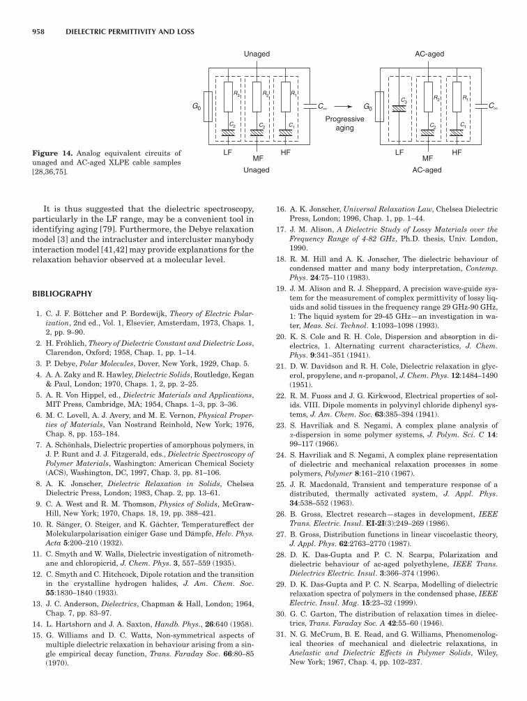
It is thus suggested that the dielectric spectroscopy,particularly in the LF range, may be a convenient tool inidentifying aging [79]. Furthermore, the Debye relaxationmodel [3] and the intracluster and intercluster manybodyinteraction model [41,42] may provide explanations for therelaxation behavior observed at a molecular level.
BIBLIOGRAPHY
1. C. J. F. Bottcher and P. Bordewijk, Theory of Electric Polar-
ization, 2nd ed., Vol. 1, Elsevier, Amsterdam, 1973, Chaps. 1,2, pp. 9–90.
2. H. Frohlich, Theory of Dielectric Constant and Dielectric Loss,Clarendon, Oxford; 1958, Chap. 1, pp. 1–14.
3. P. Debye, Polar Molecules, Dover, New York, 1929, Chap. 5.
4. A. A. Zaky and R. Hawley, Dielectric Solids, Routledge, Kegan& Paul, London; 1970, Chaps. 1, 2, pp. 2–25.
5. A. R. Von Hippel, ed., Dielectric Materials and Applications,MIT Press, Cambridge, MA; 1954, Chaps. 1–3, pp. 3–36.
6. M. C. Lovell, A. J. Avery, and M. E. Vernon, Physical Proper-
ties of Materials, Van Nostrand Reinhold, New York; 1976,Chap. 8, pp. 153–184.
7. A. Schonhals, Dielectric properties of amorphous polymers, inJ. P. Runt and J. J. Fitzgerald, eds., Dielectric Spectroscopy of
Polymer Materials, Washington: American Chemical Society(ACS), Washington, DC, 1997, Chap. 3, pp. 81–106.
8. A. K. Jonscher, Dielectric Relaxation in Solids, ChelseaDielectric Press, London; 1983, Chap. 2, pp. 13–61.
9. C. A. West and R. M. Thomson, Physics of Solids, McGraw-Hill, New York; 1970, Chaps. 18, 19, pp. 388–421.
10. R. Sanger, O. Steiger, and K. Gachter, Temperatureffect derMolekularpolarisation einiger Gase und Dampfe, Helv. Phys.Acta 5:200–210 (1932).
11. C. Smyth and W. Walls, Dielectric investigation of nitrometh-ane and chloropicrid, J. Chem. Phys. 3, 557–559 (1935).
12. C. Smyth and C. Hitchcock, Dipole rotation and the transitionin the crystalline hydrogen halides, J. Am. Chem. Soc.55:1830–1840 (1933).
13. J. C. Anderson, Dielectrics, Chapman & Hall, London; 1964,Chap. 7, pp. 83–97.
14. L. Hartshorn and J. A. Saxton, Handb. Phys., 26:640 (1958).
15. G. Williams and D. C. Watts, Non-symmetrical aspects ofmultiple dielectric relaxation in behaviour arising from a sin-gle empirical decay function, Trans. Faraday Soc. 66:80–85(1970).
16. A. K. Jonscher, Universal Relaxation Law, Chelsea DielectricPress, London; 1996, Chap. 1, pp. 1–44.
17. J. M. Alison, A Dielectric Study of Lossy Materials over the
Frequency Range of 4-82 GHz, Ph.D. thesis, Univ. London,1990.
18. R. M. Hill and A. K. Jonscher, The dielectric behaviour ofcondensed matter and many body interpretation, Contemp.
Phys. 24:75–110 (1983).
19. J. M. Alison and R. J. Sheppard, A precision wave-guide sys-tem for the measurement of complex permittivity of lossy liq-uids and solid tissues in the frequency range 29 GHz-90 GHz,1: The liquid system for 29-45 GHz—an investigation in wa-ter, Meas. Sci. Technol. 1:1093–1098 (1993).
20. K. S. Cole and R. H. Cole, Dispersion and absorption in di-electrics, 1. Alternating current characteristics, J. Chem.
Phys. 9:341–351 (1941).
21. D. W. Davidson and R. H. Cole, Dielectric relaxation in glyc-erol, propylene, and n-propanol, J. Chem. Phys. 12:1484–1490(1951).
22. R. M. Fuoss and J. G. Kirkwood, Electrical properties of sol-ids. VIII. Dipole moments in polyvinyl chloride diphenyl sys-tems, J. Am. Chem. Soc. 63:385–394 (1941).
23. S. Havriliak and S. Negami, A complex plane analysis ofa-dispersion in some polymer systems, J. Polym. Sci. C 14:99–117 (1966).
24. S. Havriliak and S. Negami, A complex plane representationof dielectric and mechanical relaxation processes in somepolymers, Polymer 8:161–210 (1967).
25. J. R. Macdonald, Transient and temperature response of adistributed, thermally activated system, J. Appl. Phys.34:538–552 (1963).
26. B. Gross, Electret research—stages in development, IEEETrans. Electric. Insul. EI-2I(3):249–269 (1986).
27. B. Gross, Distribution functions in linear viscoelastic theory,J. Appl. Phys. 62:2763–2770 (1987).
28. D. K. Das-Gupta and P. C. N. Scarpa, Polarization anddielectric behaviour of ac-aged polyethylene, IEEE Trans.Dielectrics Electric. Insul. 3:366–374 (1996).
29. D. K. Das-Gupta and P. C. N. Scarpa, Modelling of dielectricrelaxation spectra of polymers in the condensed phase, IEEE
Electric. Insul. Mag. 15:23–32 (1999).
30. G. C. Garton, The distribution of relaxation times in dielec-trics, Trans. Faraday Soc. A 42:55–60 (1946).
31. N. G. McCrum, B. E. Read, and G. Williams, Phenomenolog-ical theories of mechanical and dielectric relaxations, inAnelastic and Dielectric Effects in Polymer Solids, Wiley,New York; 1967, Chap. 4, pp. 102–237.
AC-agedUnaged
AC-agedUnaged
G0 G0
LF HFMF
LF HFMF
R1R2R3C3
C2C1
R1R2
C2C2 C1
C∞ C∞
Progressive aging
Figure 14. Analog equivalent circuits ofunaged and AC-aged XLPE cable samples[28,36,75].
958 DIELECTRIC PERMITTIVITY AND LOSS

32. C. J. Dias, Determination of a distribution relaxation fre-quency, Phys. Rev. B 53:14212–14222 (1996).
33. K. Liedermann, The calculation of a distribution of relaxationtimes from the frequency dependence of the real permittivitywith the inverse Fourier transformation, J. Non-cryst. Solids
175:21–30 (1994).
34. A. K. Jonscher, Dielectric response of polar materials, IEEETrans. Electric. Insul. 25:622–629 (1990).
35. A. K. Jonscher, The universal dielectric response and itsphysical significance, IEEE Trans. Electric. Insul., EI-19:567–577 (1992).
36. P. C. N. Scarpa, Polarization and Dielectric Behaviour of AC
Aged Polyethylene, Ph.D. thesis, Univ. Wales, 1995.
37. K. Weron, A probabilistic mechanism hidden behind the uni-versal power law for dielectric relaxation, J. Phys. Condens.
Matt. 3:9151–9162 (1991).
38. K. Weron and A. Jurlewickz, Two forms of self-similarity as afundamental feature of the power-law dielectric response,J. Phys. A Math. Gen. 26:395–410 (1993).
39. A. Weron, K. Weron, and W. A. Wyoczynski, Relaxation func-tions in dipolar materials, J. Stat. Phys. 78:1027–1038 (1995).
40. J. T. Bender and M. F. Shlesinger, Derivation of theKohlrauch-Williams/Watts decay law from activation energydispersion, Macromolecules 18:591–592 (1985).
41. L. A. Dissado and R. M. Hill, A cluster approach to the struc-ture of imperfect materials and their relaxation spectroscopy,Proc. Roy. Soc. Lond. 390:131–180 (1983).
42. L. A. Dissado and R. M. Hill, Anomalous low frequency dis-persion, J. Chem. Soc. Faraday Trans. 2 80:291–319 (1984).
43. R. M. J. Cotterill and J. C. Tallon, Melting and the liquidglassy state, J. Chem. Soc. Faraday Disc. 69:241–260 (1980).
44. H. P. Schwan, R. J. Sheppard, and E. H. Grant, Complex per-mittivity of water at 251C, J. Chem. Phys. 64:2257–2258(1976).
45. V. V. Daniel, Dielectric Relaxation, Academic Press, London;1967, Chap. 7, pp. 95–109.
46. N. E. Hill, W. E. Vaughan, and M. Davies, Dielectric Proper-
ties and Molecular Behaviour, Van Nostrand Reinhold, Lon-don; 1969, Chaps. 3–5, pp. 191–461.
47. K. H. Illinger, Dispersion and absorption of microwavesin gases and liquids, in J. B. Birks and J. Hart, eds., Progress
in Dielectrics, Academic Press, London; 1962, Vol. 4, pp.37–101.
48. H. G. Sutter, Dielectric polarization in gases, in M. Davies,ed., Dielectric and Related Molecular Processes, Chemical So-ciety, London; 1972, Vol. 1, Chap. 3, pp. 64–99.
49. E. H. Grant, T. J. Buchanan, and H. F. Cook, Dielectric be-haviour of water at microwave frequencies, J. Chem. Phys.26:156–161 (1957).
50. J. B. Hasted, Dielectric properties of water and of aqueoussolutions, in M. Davies, ed., Dielectric and Related Molecular
Processes, Chemical Society, London; 1972, Vol. 1, Chap. 5,pp. 121–161.
51. R. J. Meakins, Mechanism of dielectric absorption in solids,Progr. Dielectr. 3:151–202 (1961).
52. M. L. Williams, R. F. Landel, and J. D. Ferry, The temperaturedependence of relaxation mechanisms in amorphous poly-mers and other glass-forming liquids, J. Am. Chem. Soc.77:3701–3707 (1955).
53. D. K. Das-Gupta and R. S. Brockley, A study of absorptioncurrents in polypropylene, J. Phys. D Appl. Phys. 11:955–962(1978).
54. C. Hall, Polymer Materials: An Introduction for Technologists
and Scientists, 2nd ed., Macmillan Education, London; 1989,Chap. 2, pp. 34–54.
55. R. T. Baily, A. M. North, and R. A. Pethrick, Molecular Mo-
tions in High Polymers, Clarendon, Oxford; 1981.
56. K. Deguchi, E. Okaane, and E. Nakamura, Effects of deute-ration on the dielectric properties of ferroelectric CsH2PO4, 1.Static dielectric properties, J. Phys. Soc. Japan 51:3569–3574(1969).
57. P. R. Mason, J. B. Hasted, and L. More, The use of statisticaltheory in fitting equations to dielectric dispersion data, Adv.Mol. Rel. Proc. 6:217–232 (1974).
58. M. Shablalch, R. M. Hill, and L. A. Dissado, Dielectric exam-ination of glass-forming system, J. Chem. Soc. Faraday Trans.
2 78:639–655 (1982).
59. M. Shablakh, L. A. Dissado, and R. M. Hill, Structure anddielectric relaxation mechanisms in the cyclic alcohols, cyclo-pentanols for cyclo-octanol, J. Chem. Soc. Faraday Trans. 2
79:369–417 (1983).
60. L. A. Dissado and R. M. Hill, Dielectric behaviour of materialsundergoing dipole alignment transitions, Phil. Mag. B 41:625–642 (1980).
61. L. A. Dissado and R. M. Hill, Dynamic scaling and the firstorder character of ferroelectric transitions, J. Phys. C 16:4023–4039 (1983).
62. P. C. Hohenberg and B. I. Halperin, Theory of dynamic criticalphenomena, Rev. Mod. Phys. 49:435–479 (1977).
63. L. A. Dissado and R. M. Hill, Examination of the dielectricsusceptibility of poly-r-benzyl-L-glutamate, J. Chem. Soc.Faraday Trans. 2 78:81–93 (1982).
64. L. A. Dissado and J. C. Fothergill, Electrical Degradation and
Breakdown in Polymers, Peter Peregrinus, London; 1992,pp. 74–116.
65. L. Reich and S. A. Stivala, Elements of Polymer Degradation,McGraw-Hill, New York; 1971, pp. 1–275.
66. T. Hibma and H. R. Zeller, Direct measurement of spacecharge injection from a needle electrode into dielectrics,J. Appl. Phys. 59:1614–1620 (1986).
67. H. R. Zeller, Thermodynamics of water treeing, IEEE Trans.
Electric. Insul. EI-22:677–681 (1987).
68. R. Ross and J. J. Smit, Composition on growth of water treesin XLPE, IEEE Trans. Electric. Insul. 27:519–530 (1992).
69. E. F. Steenis, Water Treeing in Polymer Cable Insulations,KEMA Scientific Technical Report, 1990, Vol. 8, pp.149–208.
70. E. F. Steenis and F. H. Kruger, Water treeing in polyethylenecables, IEEE Trans. Electric. Insul. 5:989–1028 (1990).
71. J. J. Xu and S. A. Boggs, The chemical nature of water treeing:theories and evidence, IEEE Electric. Insul. Mag. 10(5):29–37(1994).
72. H. J. Henkel et al., Relationship between the chemical struc-ture and the effectiveness of additives in inhibiting water-trees, IEEE Trans. Electric. Insul. EI-22:157–161 (1987).
73. A. Garton et al., Oxidation and water tree formation in ser-vice-aged XLPE cable insulation, IEEE Trans. Electric. Insul.22:405–412 (1987).
74. R. J. Densley et al., Water treeing and polymer oxidation,Conf. Record, Int. Symp. Electrical Insulation, IEEE Publica-tion 90-CH2727-6, 1990, pp. 178–182.
75. P. C. N. Scarpa, A. Svatik, and D. K. Das-Gupta, Dielectricspectroscopy of polyethylene in the frequency range of 10-5 Hzto 106 Hz, Polym. Eng. Sci. 36:1072–1080 (1996).
DIELECTRIC PERMITTIVITY AND LOSS 959

76. M. Eigen, G. Kurtze, and K. Tamm, Zum Reaktions-mechanismus der Ultraschallabsorption in Wassrigen Elect-rolytlosungen, Electrochemistry 57:103–118 (1957).
77. J. C. Chan and S. M. Jaczek, The moisture absorption ofXLPE cable insulation under simulated service condition,IEEE Trans. Electric. Insul. EI-13:194–197 (1978).
78. H. Li, The Association of Ions and Electrical Properties withWater Treeing in Low Density Polyethylene, Ph.D. thesis,Univ. Strathclyde, UK, 1993.
79. D. K. Das-Gupta, Conduction mechanisms and high field ef-fects in synthetic insulating polymers, IEEE Trans. Electric.Insul. 4:149–156 (1997).
DIELECTRIC RESONATOR ANTENNAS
H. K. NG
K. W. LEUNG
City University of Hong KongKowloon, Hong Kong SAR
1. INTRODUCTION
1.1. Background
Traditionally, a dielectric resonator (DR) was used as anoscillator or a filter [1], which was treated as a source ofenergy storage rather than as an antenna. The DR wasfirst proposed as an effective radiator in 1983 by Longet al. [2]. They demonstrated the radiation capability ofthe DR with different shapes [3,4]. Henceforward, DRswere widely accepted as efficient antennas.
Researchers look for a compact, low-loss, and low-costantenna. A DR is simple in construction; it consists ofdielectric material and, therefore, has no metallic loss.This is a prominent feature especially for operation in themillimeter-wave region, where the radiation efficiency ofconventional metallic antennas is usually limited by me-tallic loss. In addition, the wavelength inside the DR issmaller than that in free space by a factor of 1=
ffiffiffiffi
erp
, whereer is the dielectric constant of the DR. Therefore, byincreasing er, it is possible to obtain a smaller antenna.
For many years, researchers have studied different DRshapes, such as cylindrical [2,5], rectangular [3], hemi-spherical [4], triangular [6,7], spherical cap [8], andcylindrical ring [9,10]. Various shapes of the dielectricresonator antenna (DRA) are shown in Fig. 1. In general,in fundamental mode a DRA radiates like a magneticdipole, a functions that is independent of antenna shape.Although DRAs are well suited for high-frequency appli-cations, only a few of them have been examined throughlimited theoretical work.
Early studies of the DRA concentrated on linear polar-ization (LP) [11–16]. Figure 2 shows the coaxial-probe-fedDRA, which was widely used for excitation of LP DRAs.However, it introduces ohmic loss and large probe self-reactance at high frequencies. Furthermore, a hole mustbe drilled in the superhard DR to accommodate the probe.This inadvertently creates undesirable airgaps [17] be-tween the probe and the DR, causing measured results to
deviate from the theoretical design. More recently, an LPDRA has been investigated using a new excitation scheme[18]: the conformal strip excitation (Fig. 3). The strip issimply cut from an adhesive conducting tape and thenmounted on the DRA surface. Since the strip does notpenetrate inside the DRA, the strip length can be adjustedvery easily. This greatly facilitates postmanufacture trim-mings of the antenna. Moreover, using this excitationmethod, the undesirable airgap between the feeding probeand the DRA [19] can be avoided. This article focuses onthe proposed conformal-strip-fed DRA. We will introducean angular displacement for the strip to have one moredegree of freedom for matching the impedance.
The circularly polarized (CP) DRA [20–24] has been avery attractive topic because, it allows a more flexibleorientation between the transmitting and receiving an-tennas than does the LP system. In addition, CP fields areless sensitive to the propagation effect than are LP fields,and the CP system is therefore widely used in satellitecommunications. A simple and straightforward CP DRAdesign utilizes a quadrature feed [5,25,26], but this sub-stantially increases the size and complexity of the feednetwork. Petosa et al. [27] shifted the complexity from thefeed network to the DRA, but the cross-shaped DRA may
(a) (b) (c)
(d) (e) (f)
Figure 1. Various DRA configurations: (a) cylindrical; (b) rec-tangular; (c) hemispherical; (d) triangular; (e) spherical cap; (f)cylindrical ring.
Coaxialprobe
Ground plane
Hemispherical DRA
Figure 2. Configuration of coaxial-probe-fed DRA.
960 DIELECTRIC RESONATOR ANTENNAS
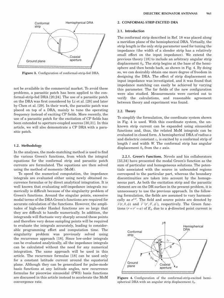
not be available in the commercial market. To avoid theseproblems, a parasitic patch has been applied to the con-formal-strip-fed DRA [20,24]. The use of a parasitic patchon the DRA was first considered by Li et al. [28] and laterby Chen et al. [29]. In their work, the parasitic patch wasplaced on top of a DRA, mainly to tune the operatingfrequency instead of exciting CP fields. More recently, theuse of a parasitic patch for the excitation of CP fields hasbeen extended to aperture-coupled sources [30,31]. In thisarticle, we will also demonstrate a CP DRA with a para-sitic patch.
1.2. Methodology
In the analyses, the mode-matching method is used to findthe various Green’s functions, from which the integralequations for the conformal strip and parasitic patchcurrents are formulated. The equations are then solvedusing the method of moments (MoM).
To speed the numerical computation, the impedanceintegrals are evaluated either using newly obtained re-currence formulas or by direct analytical integration. It iswell known that evaluating self-impedance integrals nu-merically is difficult because of the singularity problem ofGreen’s functions. Around the singular points, excessivemodal terms of the DRA Green’s functions are required foraccurate calculation of the functions. However, the ampli-tudes of high-order Hankel functions are so large thatthey are difficult to handle numerically. In addition, theintegrands will fluctuate very sharply around these pointsand therefore very dense sampling points will be requiredto evaluate the integrals accurately, leading to consider-able programming effort and computation time. Thesingularity problem was previously solved usingthe recurrence approach [18]. Since low-order integralscan be evaluated analytically, all the impedance integralscan be calculated without the need for any numericalintegration. The same approach will be used in thisarticle. The recurrence formulas [18] can be used onlyfor a constant latitude current around the equatorialplane. Although they can be generalized for pulse-modebasis functions at any latitude angles, new recurrenceformulas for piecewise sinusoidal (PWS) basis functionsare discussed in this article instead to accelerate the MoMconvergence rate.
2. CONFORMAL-STRIP-EXCITED DRA
2.1. Introduction
The conformal strip described in Ref. 18 was placed alonga meridian plane of the hemispherical DRA. Virtually, thestrip length is the only strip parameter used for tuning theimpedance (the width of a slender strip has a relativelysmall effect on the input impedance). We extend theprevious theory [18] to include an arbitrary angular stripdisplacement y0. The strip begins at the base of the hemi-sphere and then bends back, as shown in Fig. 4. By doingso, we can desirably obtain one more degree of freedom indesigning the DRA. The effect of strip displacement oninput impedance was investigated, and it was found thatimpedance matching can easily be achieved by varyingthis parameter. The far fields of the new configurationwere also studied. Measurements were carried out toverify the calculations, and reasonable agreementbetween theory and experiment was found.
2.2. Theory
To simplify the formulation, the coordinate system shownin Fig. 4 is used. With this coordinate system, the un-known strip current can be expanded using sinusoidalfunctions and, thus, the related MoM integrals can beevaluated in closed form. A hemispherical DRA of radius aand dielectric constant er is excited by a conformal strip oflength l and width W. The conformal strip has angulardisplacement y0 from the z axis.
2.2.1. Green’s Functions. Nevels and his collaborators[33,34] have presented the modal Green’s function as thesum of particular and homogeneous solutions. The poten-tials associated with the source in unbounded regionscorrespond to the particular part, whereas the boundarydiscontinuities are taken into account by the homoge-neous part. As both the excitation strip and the parasiticelement are on the DR surface in the present problem, it isunnecessary to use the previous approach. In the follow-ing formulation, the fields are assumed to vary harmoni-cally as ejot. The field and source points are denoted byr*ðr; y;fÞ and r
*0ðr0; y0;f0Þ, respectively. The Green func-
tions (r¼ r0 ¼a) of Ef due to a ff-directed point current is
Hemispherical DRAConformalstrip
Ground planeCoaxialaperture
Figure 3. Configuration of conformal-strip-fed DRA.
Groundplane
HemisphericalDRA
Conformalstrip
la
z
x
y
W
Coaxialaperture
0
r
Figure 4. Configuration of the conformal-strip-excited hemi-spherical DRA with an angular strip displacement y0.
DIELECTRIC RESONATOR ANTENNAS 961
found as follows
GEyJf¼
jZ0
2par
X
1
n¼ 0
2nþ1
nðnþ1Þ
X
n
m¼ 1
mðnmÞ!
ðnþmÞ!sin mðf f0Þ
.1
DTEn
d
dy0Pm
n ðcos y0ÞPm
n ðcos yÞsin y
Fn
(
1
DTMn
Pmn ðcos y0Þsin y0
d
dyPm
n ðcos yÞCn
)
ð1aÞ
GEf
Jf¼
jZ0
2par
X
1
n¼ 0
2nþ 1
nðnþ 1Þ
X
n
m¼ 1
ðnmÞ!
ðnþmÞ!cos mðf f0Þ
.1
DTEn Dm
d
dy0Pm
n ðcos y0Þd
dyPm
n ðcos yÞFn
(
m2
DTMn
Pmn ðcos y0Þsin y0
Pmn ðcos yÞsin y
Cn
)
ð1bÞ
where
Fn¼HHð2Þn ðk0aÞJJnðkrÞ roa
JJnðkaÞHHð2Þn ðk0rÞ r > a
(
ð1cÞ
Cn¼HH0 ð2Þn ðk0aÞJJ0nðkrÞ roa
JJ0nðkaÞHHð2Þ0
n ðk0rÞ r > a
(
ð1dÞ
It should be mentioned that the functions Fn and Cn
have different forms for the E field inside (roa) andoutside (r4a) the DR. All other symbols were defined inRefs. 35 and 36.
2.2.2. MoM. Enforcing the boundary condition that thetotal tangential electric fields should vanish on the stripsurface, we have
EsþEi¼ 0 ð2Þ
where Es and Ei are defined as the scattered and im-pressed fields due to the current density Jfs and theexcitation source, respectively. Using a delta gap sourcemodel, the impressed field can be written as ðV0=aÞdðfÞ.Then Eq. (2) can be rewritten as
1
W
ZZ
S0
GEf
JfJfsðfÞdS0 ¼
V0
adðfÞ ð3Þ
where S0 is the strip surface. Let IðfÞ¼JfsW be the stripcurrent, which is expanded as follows using the MoM
IðfÞ¼X
N
q¼ 1
IqfqðfÞ ð4Þ
where Iq are unknown expansion coefficients to be deter-mined, and fq(f) are PWS basis functions given by
fqðfÞ¼½sin keðh ajf fqjÞ= sin keh ajf fqjoh
0 elsewhere
(
ð5Þ
where h¼ 2l/(Nþ 1), fq¼ ( lþ qh)/a, and ke¼ffiffiffiffiffiffiffiffiffiffiffiffiffiffiffiffiffiffiffiffi
ðerþ 1Þ=2p
k0 are the PWS-mode half-length, the center-point of the qth expansion mode, and the effective wave-number at the DRA–air interface, respectively. Theexpansion coefficients are found via the matrix equation[Zpq][Iq]¼ [fp(0)], where Zpq are given by
Zpq¼ja2Z0
4pW2
X
1
n¼ 1
2nþ 1
nðnþ 1Þ
JJnðkaÞHHð2Þn ðk0aÞ
DTEn
(
X
n
m¼ 0
2
Dm
.ðnmÞ!
ðnþmÞ!½Y1ðn;mÞ
2Fðp; q;mÞ
JJ0nðkaÞHHð2Þn
0ðk0aÞ
DTMn
X
n
m¼ 1
2m2
.ðnmÞ!
ðnþmÞ!½Y2ðn;mÞ
2Fðp; q;mÞ
ð6Þ
Y1ðn;mÞ¼
Z y0 þW=ð2aÞ
y0W=ð2aÞ
dPmn ðcos yÞdy
sin ydy ð7Þ
Y2ðn;mÞ¼
Z y0 þW=ð2aÞ
y0W=ð2aÞ
Pmn ðcos yÞdy ð8Þ
Fðp; q;mÞ ¼2keaðcos keh cos mfhÞ
ðm keaÞðmþ keaÞ sin keh
2
cos mðfp fqÞ
ð9Þ
where
fh¼h
a sin y0ð10Þ
Since recurrence formulas exist for the integrals Y1 andY2, the integrals can be calculated very easily and quickly.Consequently, the solution (3) is a regular modal seriesthat can be implemented very straightforwardly. As thesolution can be calculated without need for any numericalintegration, it is computationally very efficient. After thestrip current is obtained, the input impedance can bereadily calculated from
Zin¼1
2P
N
q¼ 1
Iqfqð0Þ
ð11Þ
962 DIELECTRIC RESONATOR ANTENNAS

where the factor of 2 accounts for the image effect of theground plane. From the strip current the radiation can befound easily.
2.3. Results and Discussion
To verify the theory, a hemispherical DRA of a¼ 12.5 mmand er¼ 9.5 was measured using an HP8510C networkanalyzer. A conformal strip of length l¼ 12.0 mm andwidth W¼ 1.2 mm was cut from an adhesive conductingtape. For the calculation part, two basis functions and 60modal terms were used. Figure 5 shows the measured andcalculated input impedances for y0¼ 801, and reasonableagreement between theory and experiment is observed.The measured and calculated resonant frequencies are3.52 and 3.58 GHz, respectively, with error 1.7%. Theresults are consistent with the source-free value of3.68 GHz [36].
Figure 6 displays the calculated input impedance fory0¼ 601, 701, and 801. It is observed that the impedanceincreases with y0, showing that y0 can be used as a newparameter to match the impedance.
The measured and calculated far fields at 3.56 GHz forl¼ 12.0 mm, W¼ 1.2 mm, and y0¼ 801 are shown in Fig. 7,where reasonable agreement between theory and experi-ment is observed. The fields are of a broadside mode, asexpected. It is found that the copolarized field is strongerthan the cross-polarized field by more than 16 dB in the
broadside direction (y0¼01), which is sufficient for manypractical applications. Note that the H-plane cross-polar-ized field is not symmetric about the center, due to theangular displacement of the excitation strip.
3. CIRCULARLY POLARIZED DRA EXCITED BY ACONFORMAL STRIP WITH A PARASITIC PATCH
3.1. Introduction
Thus far, the work on CP DRAs has been mainly experi-mental. The first theoretical work was carried out byEsselle [21], who used the finite-difference time-domain(FDTD) method to study the CP rectangular DRA. TheFDTD method can handle a large class of problems, butsince it is purely numerical, a very long computation timeis required. Moreover, no physical insights into the pro-blem can be obtained through the numerical formulation.In this section, a CP DRA excitation method that employsa single parasitic patch is presented [24]. The conformal-strip-excited hemispherical DRA [18] is used for thedemonstration. Nevertheless, the CP technique can beused with other excitation methods and DRAs.
3.2. Theory
The configuration of the DRA is shown in Fig. 8, where ahemispherical DRA of radius a and dielectric constant er is
Frequency (GHz)
Inpu
t Im
peda
nce
(Ω)
Resistance
Reactance
TheoryExperiment
2.6 2.8 3 3.2 3.4 3.6 3.8 4 4.2 4.4–40–20
0
20
40
60
80
100
120
140
160
Figure 5. Measured and calculated input impedances for theconfiguration a¼12.5 mm, er¼9.5, l¼12.0 mm, W¼1.2 mm, andy0¼801. (From Leung and Ng [32], r 2001 John Wiley & Sons,Inc.)
Resistance
Reactance–20
0
20
40
60
80
100
120
140
3.2 3.4 3.6 3.8–40
160
3 4
Inpu
t Im
peda
nce
(Ω)
Frequency (GHz)
0 = 80
0 = 70
0 = 60
Figure 6. Calculated input impedances for y0¼601, 701, and 801,with a¼12.5 mm, er¼9.5, l¼12.0 mm, W¼1.2 mm. (From Leungand Ng [32], r 2001 John Wiley & Sons, Inc.)
TheoryExperiment
0°30°30°
60°60°
90°
Co-pol. X-pol.
(a) E-Plane
90° 90°
(b) H-Plane
0°30°
60°
30°
60°
90°
Co-pol.X-pol.
Figure 7. Measured and calculated co- and cross-polarized field patterns at f¼3.5 GHz, with a¼12.5 mm, er¼9.5, l¼12.0 mm, W¼1.2 mm. (FromLeung and Ng [32], r 2001 John Wiley & Sons, Inc.)
DIELECTRIC RESONATOR ANTENNAS 963

fed by the conformal strip of length l1 and width W1. Theparasitic patch of length l2 and width W2 is displaced at f0
from the excitation strip. Since the patch current involvesboth y and f components, in this case, integrals ofassociated Legendre functions will inevitably encoun-tered. Therefore, a convectional coordinate system isused in this section.
Image theory is used to remove the ground plane. Theequivalent imaged configuration, shown in Fig. 9, is aspherical DRA with the strip and patch lengths doubled:L1¼ 2l1 and L2¼ 2l2.
3.2.1. Green’s Functions. Since the excitation strip isassumed to be slender, it has only a longitudinal current.For the parasitic patch, however, the length-to-width ratiois arbitrary. Therefore, both the latitude and azimuthalcurrents have to be considered. The current distributionsare shown in Fig. 9. In the formulation, the superscripts A
and B refer to the excitation strip and the parasitic patch,respectively. The yy-directed current JA
y flows on the sur-face of the excitation strip. For the parasitic patch, theyy- and ff-directed patch currents are defined as JB
y and JBf ,
respectively.The yy- and ff-directed E-field Green’s functions due to a
ff-directed point current Jf have been obtained in (1a) and(1b). Now, two more Green’s functions in (12a) and (12b)are found that are due to a yy-directed point current Jy:
GEyJy¼
jZ0
2par
X
1
n¼ 0
2nþ 1
nðnþ 1Þ
X
n
m¼ 0
ðnmÞ!
ðnþmÞ!cos mðf f0Þ
.m2
DTEn
Pmn ðcos y0Þsin y0
Pmn ðcos yÞsin y
Fn
(
1
DTMn Dm
d
dy0Pm
n ðcos y0Þd
dyPm
n ðcos yÞCn
)
ð12aÞ
GEf
Jy¼
jZ0
2par
X
1
n¼0
2nþ 1
nðnþ 1Þ
X
n
m¼ 1
mðnmÞ!
ðnþmÞ!sin mðf f0Þ
.1
DTEn
Pmn ðcos y0Þsin y0
d
dyPm
n ðcos yÞFn
(
1
DTMn
d
dy0Pm
n ðcos y0ÞPm
n ðcos yÞsin y
Cn
)
ð12bÞ
3.2.2. MoM. With the Green’s functions presentedabove, the strip and patch currents can be solved by usingthe MoM. Enforcing the boundary condition that the totalE field should vanish on the conducting excitation strip,we have
AEyJyþ BEy
Jyþ BEy
JfþEi¼ 0 ð13Þ
a
W1
Grounded parasitic patch
Hemispherical DRA
Conformalexcitationstrip
Coaxialaperture
Ground plane
l1 l2
z
x
y
0
W2
Figure 8. Configuration of conformal-strip-excited DRA with a parasitic patch. (FromLeung and Ng [24], 2003 r IEEE.)
2l1 2l2
W1
W2
JA
JB
J B
Figure 9. Equivalent geometry of the DRA configuration.
964 DIELECTRIC RESONATOR ANTENNAS

where Ei is the impressed E field on the excitation strip.Equation (13) can be rewritten in terms of Green’s func-tions,
ZZ
SA
GEyJy
JAy dS0 þ
ZZ
SB
GEyJy
JBy dS0 þ
ZZ
SB
GEyJf
JBfdS0 þEi¼ 0
ð14Þ
where SA and SB are the surfaces of the excitation stripand parasitic patch, respectively. For simplicity, the deltagap source is used again to model the excitation,Ei¼ ðV0=aÞdðyÞ, where V0 is the excitation voltage and isset to unity for convenience. Let IA
y ¼JAy W1 be the excita-
tion strip current and IBy ¼JB
y W2, IBf ¼JB
fL2; then (14)becomes
1
W1
ZZ
SA
GEyJy
IAy dS0 þ
1
W2
ZZ
SB
GEyJy
IBy dS0
þ1
L2
ZZ
SB
GEyJf
IBfdS0 ¼
1
adðyÞ
ð15Þ
The next step is to expand the currents using the MoMas follows
IAy ðyÞ¼
X
N1
p1 ¼ 1
IyAp1
f yAp1ðyÞ ð16Þ
IBy ðyÞ¼
X
N2
p2 ¼ 1
IyBp2
f yBp12ðyÞ ð17Þ
IBf ðfÞ¼
X
N3
p3 ¼ 1
IfBp3
f fBp3ðfÞ ð18Þ
where f yAp1ðyÞ, f yB
p2ðyÞ, and f fB
p3ðfÞ are PWS basis functions
given by
f yAp1ðyÞ¼
sinðyAh jy yA
p1jÞ
sin yAh
; ajy yAp1joh1
0 elsewhere
8
>
<
>
:
ð19Þ
f yBp2ðyÞ¼
sinðyBh jy yB
p2jÞ
sin yBh
; ajy yBp2joh2
0 elsewhere
8
>
<
>
:
ð20Þ
f fBp2ðfÞ¼
sin keðh3 ajf fBp3jÞ
sin k0h3; ajf fB
p3joh3
0 elsewhere
8
>
<
>
:
ð21Þ
in which
yAh ¼
h1
a; yA
p1¼
p2
L1
2aþp1y
Ah ; h1¼
L1
N1þ 1ð22Þ
yBh ¼
h2
a; yB
p2¼
p2
L2
2aþp2y
Bh ; h2¼
L2
N2þ1ð23Þ
fBh ¼
h3
a; fB
p3¼f0
W2
2aþp3f
Bh ; h3¼
W2
N3þ 1ð24Þ
and ke¼ffiffiffiffiffiffiffiffiffiffiffiffiffiffiffiffiffiffiffiffi
ðerþ 1Þ=2p
k0 is the effective wavenumber at theDRA–air interface. By employing the Galerkin procedure,we multiply both sides of (15) by f yA
q1ðyÞ (1rq1rN1) and
integrate the result over the strip surface, yielding
1
W21
X
N1
p1 ¼ 1
IyAp1
ZZ
S¼SA
ZZ
S 0 ¼SA
f yAq1ðyÞGEy
Jyf yAp1ðy0ÞdS0dS
þ1
W1W2
X
N2
l¼ 1
IyBp2
ZZ
S¼SA
ZZ
S 0 ¼SB
f yAq1ðyÞGEy
Jyf yBp2ðy0ÞdS0dS
þ1
W1L2
X
N3
n¼ 1
IfBp3
ZZ
S¼SA
ZZ
S 0 ¼SB
f yAq1ðyÞGEy
Jff fBp3ðy0ÞdS0dS
¼
Z p=2þ l1=a
p=2l1=af yAq1ðyÞdðyÞdðyÞ ð25Þ
Similarly, two more integral equations can be obtainedby enforcing the following boundary conditions on theparasitic patch:
AEfJyþ BEf
Jyþ BEf
Jf¼ 0 ð26aÞ
AEyJyþ BEW
Jyþ BEy
Jf¼ 0 ð26bÞ
Applying the Galerkin procedure again, we multiply thetwo equations by f yB
q2ðyÞ (1rq2rN2) and f yB
q3ðfÞ
(1rq3rN3), respectively. Totally, there are three sets ofequations with three sets of unknowns, which can besolved via the following matrix equation
½ZAA 0
yy ðp1; q1ÞN1N1½ZAB 0
yy ðp1; q2ÞN1N2½ZAB 0
yf ðp1; q3ÞN1N3
½ZBA 0
yy ðp2; q1ÞN2 N1½ZBB 0
yy ðp2; q2ÞN2N2½ZBB 0
yf ðp2; q3ÞN2 N3
½ZBA 0
fy ðp3; q1ÞN3N1½ZBB 0
fy ðp3; q2ÞN3N2½ZBB 0
ff ðp3; q3ÞN3N3
2
6
6
6
6
4
3
7
7
7
7
5
.
½IyAp1N1 1
½IyBp2N2 1
½IfBp3N3 1
2
6
6
6
6
4
3
7
7
7
7
5
¼
½VAq1N1 1
½0N2 1
½0N3 1
2
6
6
6
4
3
7
7
7
5
ð27Þ
DIELECTRIC RESONATOR ANTENNAS 965

where, for X,Y¼A or B and a,b¼ y or f, we obtain
ZXY 0
ab ðp; qÞ¼1
GXa G
Yb
ZZ
S¼SX
ZZ
S 0 ¼SY
f aXp ðaÞG
EaJb
f bYq ðb
0ÞdS0dS
ð28Þ
VAq1¼
Z p=2þ l1=a
p=2l1=af yAq1ðyÞdðyÞdy ð29Þ
with GA;By ¼W1;2 and GB
y ¼L2. For the voltage matrix ½VAq1,
the center element is equal to unity but all the otherelements are zero. After the current vector ½IyA
p1 is obtained
from (27), the input impedance can be calculated fromZin¼ g=
PN1
p1 ¼ 1 IyAp1
f yAp1ð0Þ, where g ¼ 1 for the equivalent
spherical structure and 12 for the original hemispherical
structure. The other two current vectors ½IyBp2, ½IfB
p3, to-
gether with ½IyAp1, will be used to calculate the radiation
fields of the antenna. To this end, the key step is toevaluate the various impedance elements ZXY 0
ab , whichwill be discussed next.
3.2.3. Evaluation of Z Matrix. Numerical evaluation ofZXY 0
ab will be very difficult when X¼Y, since the field andsource points may coincide in this case, causing thesingular problem to occur. Using the previous approach[18], all ZXY 0
ab can be calculated without the need for anynumerical integration. Thus, the computation time andprogramming effort are greatly reduced. To begin with,the Green’s functions (1) and (12) are substituted into (29)to get nine different expressions:
ZAA0
yy ðp1; q1Þ¼ ja2Z0
2pW21
X
1
n¼ 1
.X
n
m¼ 0
rTEðn;mÞ .m2 .YA
1 ðp1;n;mÞ
(
YA1 ðq1;n;mÞ .F1ðm;fA;fAÞ
X
n
m¼ 0
rTMðn;mÞ
Dm
.YA2 ðp1;n;mÞ
YA2 ðq1;n;mÞ .F1ðm;fA;fAÞ
ð30Þ
ZAB0
yy ðp1; q2Þ¼ ja2Z0
2pW1W2
X
1
n¼1
.X
n
m¼ 0
rTEðn;mÞ .m2 .YA
1 ðp1;n;mÞ
(
YB1 ðq2;n;mÞ .F1ðm;fA;fBÞ
X
n
m¼ 0
rTMðn;mÞ
Dm
.YA2 ðp1;n;mÞ
YB2 ðq2;n;mÞF1ðm;fA;fBÞ
ð31Þ
ZAB0
yf ðp1; q3Þ¼ ja2Z0
2pW1L2
X
1
n¼ 1
.X
n
m¼ 0
rTEðn;mÞ .m .YA1 ðp1;n;mÞ
(
YB4 ðn;mÞ .F2ðq3;m;fA;fBÞ
X
n
m¼ 0
rTMðn;mÞ .m .YA2 ðp1;n;mÞ
YB3 ðn;mÞ .F2ðq3;m;fA;fBÞ
ð32Þ
ZBA0
yy ðp2; q1Þ¼ ja2Z0
2pW1W2
X
1
n¼ 1
.X
n
m¼ 0
rTEðn;mÞ .m2 .YB
1 ðp2;n;mÞ
(
YA1 ðq1;n;mÞ .F1ðm;fB;fAÞ
X
n
m¼ 0
rTMðn;mÞ
DmYB
2 ðp2;n;mÞ
YA2 ðq1;n;mÞ .F1ðm;fB;fAÞ
ð33Þ
ZBB0
yy ðp2;q2Þ¼ ja2Z0
2pW22
X
1
n¼ 1
.X
n
m¼ 0
rTEðn;mÞ .m2 .YB
1 ðp2;n;mÞ
(
YB1 ðq2;n;mÞ .F1ðm;fB;fBÞ
X
n
m¼ 0
rTMðn;mÞ
DmYB
2 ðp2;n;mÞ
YB2 ðq2;n;mÞ .F1ðm;fB;fBÞ
ð34Þ
ZBB0
yf ðp2; q3Þ¼ ja2Z0
2pW2L2
X
1
n¼ 1
.X
n
m¼ 0
rTEðn;mÞ .m .YB1 ðp2;n;mÞ
(
YB4 ðn;mÞ .F2ðq3;m;fB;fBÞ
X
n
m¼ 0
rTMðn;mÞ .m .YB2 ðp2;n;mÞ
YB3 ðn;mÞ .F2ðq3;m;fB;fBÞ
ð35Þ
966 DIELECTRIC RESONATOR ANTENNAS

ZBA0
fy ðp3; q1Þ¼ ja2Z0
2pW1L2
X
1
n¼ 1
.X
n
m¼ 0
rTEðn;mÞ .m .YB4 ðn;mÞ
(
YA1 ðq3;n;mÞ .F2ðp1;m;fB;fAÞ
X
n
m¼ 0
rTMðn;mÞ .m .YB3 ðn;mÞ
YA2 ðq3;n;mÞ .F2ðp1;m;fB;fAÞ
ð36Þ
ZBB0
fy ðp3; q2Þ¼ ja2Z0
2pW2L2
X
1
n¼ 1
.X
n
m¼0
rTEðn;mÞ .m .YB4 ðn;mÞ
(
YB0
1 ðq2;n;mÞF2ðp3;m;fB;fBÞ
X
n
m¼ 0
rTMðn;mÞ .m .YB3 ðn;mÞ
YB0
2 ðq2;n;mÞ .F2ðp3;m;fB;fBÞ
ð37Þ
ZBB0
ff ðp3; q3Þ¼ ja2Z0
2pL22
X
1
n¼ 1
.X
n
m¼0
rTEðn;mÞ
DmYB
4 ðn;mÞ
(
YB0
4 ðn;mÞ .F3ðp3; q3;m;fB;fBÞ
X
n
m¼ 0
rTMðn;mÞ .m2 .YB
3 ðn;mÞ
YB0
3 ðn;mÞ .F3ðp3; q3;m;fB;fBÞ
ð38Þ
where
rTEðn;mÞ¼2nþ 1
nðnþ1Þ.
JJnðkaÞHHð2Þn ðk0aÞ
DTEn
.ðnmÞ!
ðnþmÞ!
ð39Þ
rTMðn;mÞ¼2nþ 1
nðnþ 1Þ.
JJnðkaÞHHð2Þn0ðk0aÞ
DTMn
.ðnmÞ!
ðnþmÞ!
ð40Þ
F1ðm;fX ;fY Þ
¼
Z fX2
fX1
Z fY2
fY1
cos mðf f0Þdf0 dfð41Þ
F2ðp;m;fX ;fY Þ
¼
Z fX2
fX1
Z fY2
fY1
sin mðf f0Þf fYp ðfÞdf
0 df ð42Þ
F3ðp; q;m;fBÞ
¼
Z fB2
fB1
Z fB2
fB1
f fBp ðfÞ cos mðf f0Þ
f fBq ðf
0Þdf0 df
ð43Þ
YX1 ðp;n;mÞ
¼
Z yXp þ yX
h
yXpy
Xh
Pmn ðcos yÞf yX
p ðyÞdyð44Þ
YX2 ðp;n;mÞ
¼
Z yXp þ yX
h
yXpy
Xh
dPmn ðcos yÞ
dysin y f yX
p ðyÞdyð45Þ
YB3 ðn;mÞ¼
Z p=2þ l2=a
p=2l2=aPm
n ðcos yÞdy ð46Þ
YB4 ðn;mÞ¼
Z p=2þ l2=a
p=2l2=a
dPmn ðcos yÞ
dysin ydy ð47Þ
and
fA1¼ W1=2a; fA2¼W1=2a; fB1¼f0 W2=2a;
and fB2¼f0þW2=2að48Þ
The integrals will be evaluated by either using therecurrence technique or analytical integration. This willbe discussed in the following paragraphs.
3.2.3.1. YX1 ðp; n;mÞ and YX
2 ðp; n;mÞ. To evaluateYX
1 ðp;n;mÞ and YX2 ðp;n;mÞ (X¼A or B) analytically, the
absolute sign of the PWS functions f yAp ðyÞ (19) and f yB
p ðyÞ(20) is first removed by breaking each integral into twoparts. After several mathematical manipulations, the
DIELECTRIC RESONATOR ANTENNAS 967

following results are obtained
YX1 ðp;n;mÞ¼
1
sin yXh
½sinðyXh yX
p ÞI1ðn;mÞ
þ cosðyXh yX
p ÞI10ðn;mÞ
þ sinðyXh þ yX
p ÞI2ðn;mÞ
cosðyXh þ yX
p ÞI20ðn;mÞ
ð49Þ
YX2 ðp;n;mÞ¼
1
sin yXh
½sinðyXh yX
p ÞI3ðn;mÞ
þ cosðyXh yX
p ÞI30ðn;mÞ
þ sinðyXh þ yX
p ÞI4ðn;mÞ
cosðyXh þ yX
p ÞI40ðn;mÞ
ð50Þ
where
I1;2ðn:mÞ¼ xffiffiffiffiffiffiffiffiffiffiffiffiffiffi
1 x2p
Pmn ðxÞ
h ix2
x1
þKðm;nÞ 2
2nþ1
.1
2nþ 3K
ðnþ 2;mþ 2Þ
1
2nþ 3þ
1
2n 1
Kðn;mþ 2Þ
þ1
2n 1Kðn 2;mþ 2Þ
ð51Þ
I1;20ðn;mÞ¼
nðnmþ 1Þ
ð2nþ 1Þð2nþ 3ÞKðnþ 2;mþ 1Þ
þðnþ1ÞðnþmÞ
ð2nþ 1Þð2n 1Þþ
nðnmþ 1Þ
ð2nþ1Þð2nþ 3Þ
.Kðn;mþ 1Þ ðnþ 1ÞðnþmÞ
ð2nþ 1Þð2n 1ÞKðn 2;mþ1Þ
ð52Þ
I3;4ðn;mÞ¼ðnmþ 1Þ
2nþ 1Kðnþ 1;mÞ
mþn
2nþ 1Kðn 1;mÞ
ð53Þ
I3;40ðn;mÞ¼
1
2nþ 1fKðnþ 1;mþ 1Þ
Kðn 1;mþ 1Þg
ð54Þ
in which
Kðn;mÞ¼
Z x2
x1
Pmn ðxÞffiffiffiffiffiffiffiffiffiffiffiffiffiffi
1 x2p dx ð55Þ
with ½f ðxÞx2x1¼ f ðx2Þ f ðx1Þ. x1¼ cosðyX
p yXh Þ, x2¼ cos yX
p
for I1;3; I1;30 and x1¼ cos yX
p , x2¼ cosðyXp þ yX
h Þ for I2;4; I2;40.
For K(n,m), the recurrence formulas with arbitrary x1, x2
have been obtained [37] as follows
Kðnþ 1;mÞ¼ð2nþ 1Þ
ðnþ 1Þðnmþ 1Þ
ffiffiffiffiffiffiffiffiffiffiffi
1 xp
Pmnþ 1ðxÞ
h ix2
x1
þnðnþmÞKðn 1;mÞ
ð56Þ
Kðn;mþ 1Þ¼ 2½Pmþ 1n ðxÞx2
x1
þ ðnþmÞðnmþ 1ÞKðn;m 1Þð57Þ
with initial values given by
Kð0; 0Þ¼ ½sin1ðxÞx2
x1; Kð1; 0Þ¼ ½1 x2x2x1;
Kðn; 1Þ¼ ½PnðxÞx2x1
ð58Þ
3.2.3.2. YB3 ðn;mÞ and YB
4 ðn;mÞ. The integrals YB3 ðn;mÞ
and YB4 ðn;mÞ were studied in [18, Eqs. (11) and (12)], and
the results are given by
YB3 ðnþ1;mÞ¼
1
ðnþ 1Þðnmþ 1Þ
ð2nþ 1Þ 1 ð1Þnþm
ffiffiffiffiffiffiffiffiffiffiffiffiffiffi
1 x2b
q
Pmn ðxbÞþnðnþmÞYB
3 ðn 1;mÞ
ð59Þ
YB3 ðn;mþ 2Þ¼ 2½1 ð1Þnþm
Pmþ 1n ðxbÞ
þ ðnþmþ 1ÞðnmÞYB3 ðn;mÞ
ð60Þ
where
xb¼ cosp2
l2
a
¼ sinl2
að61Þ
and the initial values are
YB3 ðn; 0Þ¼YB
3 ðn; 1Þ¼ ½ð1Þn 1PnðxbÞ ð62Þ
The integral YB3 ðn;mÞ can be expressed in terms of
YB4 ðn;mÞ, which is given by
YB4 ðn;mÞ¼ ½ð1Þnþm
1ffiffiffiffiffiffiffiffiffiffiffiffiffiffi
1 x2b
q
Pmn ðxbÞ
1
2nþ 1½ðnþmÞYB
3 ðn 1;mÞ
ðm n 1ÞYB3 ðnþ 1;mÞ
ð63Þ
3.2.3.3. F2ðp;m;fX ;fY Þ. The integrals F2ðp;m;fX ;fY Þ
are zero when m¼ 0. When m 6¼ 0, the integration can be
968 DIELECTRIC RESONATOR ANTENNAS
performed analytically. The result is given by
F2¼2kea
sin keh
.½cos mðfX2fpÞcos mðfX1fpÞðcos kehcos mfB
h Þ
ðm keaÞðmþ keaÞ
ð64Þ
The last integral F3ðp; q;m;fBÞ is given by (9). Now allthe integrals can be evaluated analytically. Note that ZXY 0
abare simply regular series that can be implemented easilyin a straightforward manner.
3.2.4. Evaluation of Radiation Field Patterns. The farfield of the antenna comprises radiation from the excita-tion strip current IA
y and parasitic patch current compo-nents IB
y ; IBf . The electric far field is given by
Ey;fðr; y;fÞ
¼jZ0a
2pW1
.ejk0r
r
X
N1
p1 ¼ 1
IyAp1
.EA 0
yy;yfðp1; y;fÞ
þjZ0a
2pW2
.ejk0r
r
X
N2
p2 ¼ 1
IyBp2
.EB 0
yy;yfðp2; y;fÞ
jZ0a
2pL2
.ejk0r
r
X
N3
p3 ¼ 1
IfBp3
.EB 0
yf;ffðp3; y;fÞ
ð65Þ
in which
EX 0
yy ðp; y;fÞ¼X
1
n¼1
jn2nþ 1
nðnþ 1Þ
jJJnðkaÞ
DTEn
(
X
n
m¼ 0
m2 ðnmÞ!
ðnþmÞ!
Pmn ðcos yÞsin y
YX1 ðp;n;mÞF4ðm;fÞ
JJn0ðkaÞ
DTMn
X
n
m¼ 0
1
Dm
ðnmÞ!
ðnþmÞ!
dPmn ðcos yÞ
dy
YX1 ðp;n;mÞF4ðm;fÞ
ð66Þ
EX 0
yfðp; y;fÞ¼X
1
n¼ 1
jn2nþ 1
nðnþ 1Þ
jJJnðkaÞ
DTEn
(
X
n
m¼0
mðnmÞ!
ðnþmÞ!
dPmn ðcos yÞ
dy
YX2 ðp;n;mÞF5ðm;fÞ
JJn0ðkaÞ
DTMn
X
n
m¼0
mðnmÞ!
ðnþmÞ!
Pmn ðcos yÞsin y
YX5 ðp;n;mÞF5ðm;fÞ
ð67Þ
EB 0
fyðp; y;fÞ ¼X
1
n¼ 1
jn2nþ 1
nðnþ 1Þ
jJJnðkaÞ
DTMn
(
X
n
m¼ 0
mðnmÞ!
ðnþmÞ!
dPmn ðcos yÞ
dy
YB3 ðn;mÞF6ðp;m;fÞ
JJn0ðkaÞ
DTEn
X
n
m¼ 0
mðnmÞ!
ðnþmÞ!
Pmn ðcos yÞsin y
YB3 ðn;mÞF6ðp;m;fÞ
ð68Þ
EB 0
ffðp; y;fÞ¼X
1
n¼ 1
jn2nþ 1
nðnþ 1Þ
jJJnðkaÞ
DTMn
(
X
n
m¼ 0
m2 ðnmÞ!
ðnþmÞ!
Pmn ðcos yÞsin y
YB4 ðn;mÞF7ðp;m;fÞ
JJn0ðkaÞ
DTEn
X
n
m¼ 0
1
Dm
ðnmÞ!
ðnþmÞ!
dPmn ðcos yÞ
dy
YB4 ðn;mÞF7ðp;m;fÞ
ð69Þ
where, for X¼A or B
FX4 ðm;fÞ ¼
Z fX2;X2
fX1;X1
sin mðf f0Þdf0 ð70Þ
FX5 ðm;fÞ¼
Z fX2;X2
fX1;X1
cos mðf f0Þdf0 ð71Þ
FB6 ðp;m;fÞ¼
Z fB2
fB1
sin mðf f0Þf fBp ðf
0Þdf0 ð72Þ
FB7 ðp;m;fÞ¼
Z fB2
fB1
cos mðf f0Þf fBp ðf
0Þdf0 ð73Þ
The integrals FX4 ðm;fÞ (70) and FX
5 ðm;fÞ (71) can easilybe evaluated in a single step. For F6ðp;m;fÞ andF7ðp;m;fÞ, the results were obtained previously [38,p. 302] and are summarized here:
FX4 ðm;fÞ
¼
1m ½cos mðf fX2Þ cos mðf fX1Þ mO0
0 m¼ 0
8
<
:
ð74Þ
FX5 ðm;fÞ
¼
1m ½sin mðf fX2Þ sin mðf fX1Þ mO0
0 m¼ 0
8
<
:
ð75Þ
DIELECTRIC RESONATOR ANTENNAS 969
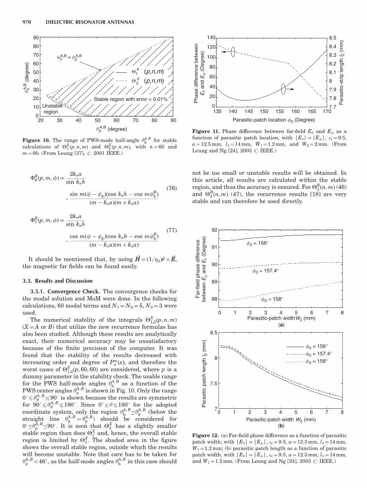
FB6 ðp;m;fÞ¼
2kea
sin keh
.sin mðf fpÞðcos keh cos mfB
h Þ
ðm keaÞðmþ keaÞ
ð76Þ
FB7 ðp;m;fÞ¼
2kea
sin keh
.cos mðf fpÞðcos keh cos mfB
h Þ
ðm keaÞðmþ keaÞ
ð77Þ
It should be mentioned that, by using ~HH¼ ð1=Z0Þrr~EE,
the magnetic far fields can be found easily.
3.3. Results and Discussion
3.3.1. Convergence Check. The convergence checks forthe modal solution and MoM were done. In the followingcalculations, 60 modal terms and N1¼N2¼ 5, N3¼ 3 wereused.
The numerical stability of the integrals YX1;2ðp;n;mÞ
(X¼A or B) that utilize the new recurrence formulas hasalso been studied. Although these results are analyticallyexact, their numerical accuracy may be unsatisfactorybecause of the finite precision of the computer. It wasfound that the stability of the results decreased withincreasing order and degree of Pm
n ðxÞ, and therefore theworst cases of YX
1;2ðp;60; 60Þ are considered, where p is adummy parameter in the stability check. The usable rangefor the PWS half-mode angles yA;B
h as a function of thePWS center angles yA;B
p is shown in Fig. 10. Only the range01ryp
A, Br901 is shown because the results are symmetricfor 901ryp
A, Br1801. Since 01ryr1801 for the adoptedcoordinate system, only the region yA;B
h yA;Bp (below the
straight line yA;Bh ¼ yA;B
p ) should be considered for0yA;B
p 90. It is seen that YX2 has a slightly smaller
stable region than does YX1 and, hence, the overall stable
region is limited by YX1 . The shaded area in the figure
shows the overall stable region, outside which the resultswill become unstable. Note that care has to be taken foryA;B
p o46, as the half-mode angles yA;Bh in this case should
not be too small or unstable results will be obtained. Inthis article, all results are calculated within the stableregion, and thus the accuracy is ensured. For YB
3 ðn;mÞ (46)and YB
4 ðn;mÞ (47), the recurrence results [18] are verystable and can therefore be used directly.
(degree)
20 30 40 50 60 70 80 900
10
20
30
40
50
60
70
80
90
Unstable region
Stable region with error < 0.01%
(p,n,m)
(p,n,m)1X
2X
pA,B
(deg
ree)
hA
,B
hA,B p
A,B=
Θ
Θ
Figure 10. The range of PWS-mode half-angle yA;Bh for stable
calculations of YX1 ðp;n;mÞ and YX
2 ðp;n;mÞ, with n¼60 andm¼60. (From Leung [37], r 2001 IEEE.)
135 140 145 150 155 160 165 1700
20
40
60
80
100
120
140
7.7
7.8
7.9
8
8.1
8.2
8.3
8.4
8.5
Par
asiti
c-st
rip le
ngth
l 2 (
mm
)
Pha
se d
iffer
ence
bet
wee
nE
an
d E
(
Deg
ree)
Parasitic-patch location 0 (Degree)
Figure 11. Phase difference between far-field Ey and Ef as afunction of parasitic patch location, with |Ey|¼|Ef|, er¼9.5,a¼12.5 mm, l1¼14 mm, W1¼1.2 mm, and W2¼2 mm. (FromLeung and Ng [24], 2003 r IEEE.)
Parasitic-patch width W2 (mm)
Par
asiti
c pa
tch
leng
th l 2
(m
m)
0 1 2 3 4 5 6 7 87
7.5
8
8.5
0 = 156° 0 = 157.4° 0 = 158°
0 1 2 3 4 5 6 7 8
88
89
90
91
92
Far
-fie
ld p
hase
diff
eren
cebe
twee
n E
a
nd E
(D
egre
e)
0 = 156°
0 = 157.4°
0 = 158°
Parasitic-patch widthW2 (mm)(a)
(b)
Figure 12. (a) Far-field phase difference as a function of parasiticpatch width, with |Ey|¼|Ef|, er¼9.5, a¼12.5 mm, l1¼14 mm,W1¼1.2 mm; (b) parasitic patch length as a function of parasiticpatch width, with |Ey|¼|Ef|, er¼9.5, a¼12.5 mm, l1¼14 mm,and W1¼1.2 mm. (From Leung and Ng [24], 2003 r IEEE.)
970 DIELECTRIC RESONATOR ANTENNAS
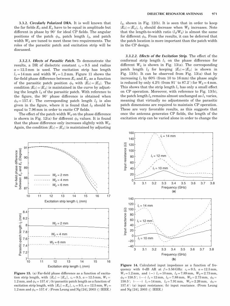
3.3.2. Circularly Polarized DRA. It is well known thatthe far fields Ey and Ef have to be equal in amplitude butdifferent in phase by 901 for ideal CP fields. The angularpositions of the patch f0, patch length l2, and patchwidth W2 are tuned to meet these two requirements. Theroles of the parasitic patch and excitation strip will bediscussed.
3.3.2.1. Effects of Parasitic Patch. To demonstrate theresults, a DR of dielectric constant er¼9.5 and radiusa¼ 12.5 mm is used. The excitation strip has lengthl1¼14 mm and width W1¼1.2 mm. Figure 11 shows thefar-field phase difference between Ey and Ef as a functionof the parasitic patch position f0 with jEyj ¼ jEfj. Thecondition jEyj ¼ jEfj is maintained in the curve by adjust-ing the length l2 of the parasitic patch. With reference tothe figure, the 901 phase difference is obtained whenf0¼ 157.41. The corresponding patch length l2 is alsogiven in the figure, where it is found that l2 should beequal to 7.96 mm in order to excite CP fields.
The effect of the patch width W2 on the phase differenceis shown in Fig. 12(a) for different f0 values. It is foundthat the phase difference only increases slightly with W2.Again, the condition jEyj ¼ jEfj is maintained by adjusting
l2, shown in Fig. 12(b). It is seen that in order to keepjEyj ¼ jEfj, l2 should decrease when W2 increases. Notethat the length-to-width ratio (l2/W2) is almost the samefor different f0. From the results, it can be deferred thatthe patch location is more important than the patch widthin the CP design.
3.3.2.2. Effects of the Excitation Strip. The effect of theconformal strip length l1 on the phase difference fordifferent W2 is shown in Fig. 13(a). The correspondingpatch length l2 for keeping jEyj ¼ jEfj is shown inFig. 13(b). It can be observed from Fig. 13(a) that byincreasing l1 by 60% (from 10 to 16 mm) the phase angleis reduced by only 4.2% (from 911 to 87.21) for W2¼ 4 mm.This shows that the strip length l1 has only a small effecton CP operation. Moreover, with reference to Fig. 13(b),the patch length l2 remains almost unchanged as l1 varies,meaning that virtually no adjustments of the parasiticpatch dimensions are required to maintain CP operation.These are very favorable results, as this suggests thatonce the antenna generates CP fields, the length of theexcitation strip can be varied alone in order to change the
Excitation strip length l1 (mm)
10 11 12 13 14 15 16 17
87
88
89
90
91
W2 = 2 mm
W2 = 4 mm
W2 = 6 mmFar
-fie
ld p
hase
diff
eren
cebe
twee
n E
a
nd E
(D
egre
e)P
aras
itic-
patc
h le
ngth
l 2 (
mm
)
10 11 12 13 14 15 167
7.2
7.4
7.6
7.8
8
8.2
8.4
W2 = 4 mm
W2 = 2 mm
W2 = 6 mm
Excitation strip length l1 (mm)
Figure 13. (a) Far-field phase difference as a function of excita-tion strip length, with |Ey|¼|Ef|, er¼9.5, a¼12.5 mm, W1¼
1.2 mm, and f0¼157.41; (b) parasitic patch length as a function ofexcitation strip length, with |Ey|¼Ef|, er¼9.5, a¼12.5 mm, W1¼
1.2 mm and f0¼157.41. (From Leung and Ng [24], 2003 r IEEE.)
3 3.1 3.2 3.3 3.4 3.5 3.6 3.7 3.80
20
40
60
80
100
120
140
160l1 = 14 mm
l1 = 12 mm
l1 = 10 mmInpu
t res
ista
nce
(Ω)
Frequency (GHz)(a)
3 3.1 3.2 3.3 3.4 3.5 3.6 3.7 3.8–40
–20
0
20
40
60
80
100
120
140
Inpu
t rea
ctan
ce (
Ω)
l1 = 14 mm
l1 = 12 mm
l1 = 10 mm
Frequency (GHz)
(b)
Figure 14. Calculated input impedance as a function of fre-quency with 0-dB AR at f¼3.56 GHz: er¼9.5, a¼12.5 mm,W1¼1.2 mm, and (—) l1¼10 mm, l2¼7.89 mm, W2¼2.73 mm,f0¼158.51; (- - -) l1¼12 mm, l2¼7.88 mm, W2¼2.73 mm, f0¼
158.51; (- - -) l1¼14 mm, l2¼7.91 mm, W2¼2.26 mm, f0¼
157.41: (a) input resistance; (b) input reactance. (From Leungand Ng [24], 2003 r IEEE.)
DIELECTRIC RESONATOR ANTENNAS 971
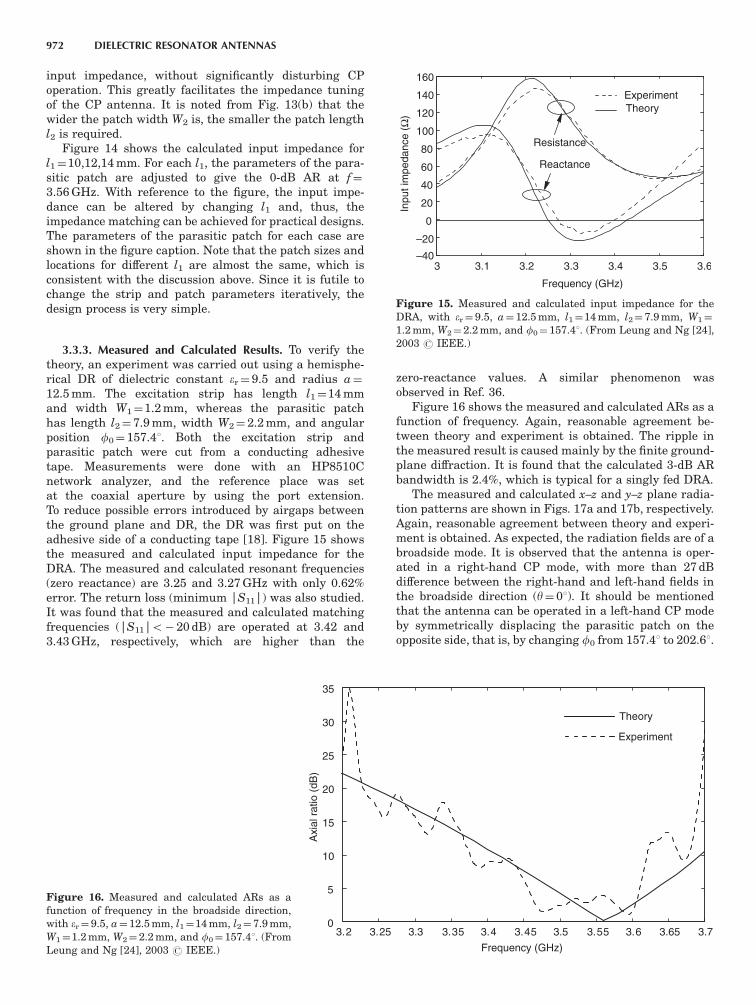
input impedance, without significantly disturbing CPoperation. This greatly facilitates the impedance tuningof the CP antenna. It is noted from Fig. 13(b) that thewider the patch width W2 is, the smaller the patch lengthl2 is required.
Figure 14 shows the calculated input impedance forl1¼10,12,14 mm. For each l1, the parameters of the para-sitic patch are adjusted to give the 0-dB AR at f¼3.56 GHz. With reference to the figure, the input impe-dance can be altered by changing l1 and, thus, theimpedance matching can be achieved for practical designs.The parameters of the parasitic patch for each case areshown in the figure caption. Note that the patch sizes andlocations for different l1 are almost the same, which isconsistent with the discussion above. Since it is futile tochange the strip and patch parameters iteratively, thedesign process is very simple.
3.3.3. Measured and Calculated Results. To verify thetheory, an experiment was carried out using a hemisphe-rical DR of dielectric constant er¼ 9.5 and radius a¼12.5 mm. The excitation strip has length l1¼14 mmand width W1¼1.2 mm, whereas the parasitic patchhas length l2¼ 7.9 mm, width W2¼ 2.2 mm, and angularposition f0¼ 157.41. Both the excitation strip andparasitic patch were cut from a conducting adhesivetape. Measurements were done with an HP8510Cnetwork analyzer, and the reference place was setat the coaxial aperture by using the port extension.To reduce possible errors introduced by airgaps betweenthe ground plane and DR, the DR was first put on theadhesive side of a conducting tape [18]. Figure 15 showsthe measured and calculated input impedance for theDRA. The measured and calculated resonant frequencies(zero reactance) are 3.25 and 3.27 GHz with only 0.62%error. The return loss (minimum |S11|) was also studied.It was found that the measured and calculated matchingfrequencies (|S11|o 20 dB) are operated at 3.42 and3.43 GHz, respectively, which are higher than the
zero-reactance values. A similar phenomenon wasobserved in Ref. 36.
Figure 16 shows the measured and calculated ARs as afunction of frequency. Again, reasonable agreement be-tween theory and experiment is obtained. The ripple inthe measured result is caused mainly by the finite ground-plane diffraction. It is found that the calculated 3-dB ARbandwidth is 2.4%, which is typical for a singly fed DRA.
The measured and calculated x–z and y–z plane radia-tion patterns are shown in Figs. 17a and 17b, respectively.Again, reasonable agreement between theory and experi-ment is obtained. As expected, the radiation fields are of abroadside mode. It is observed that the antenna is oper-ated in a right-hand CP mode, with more than 27 dBdifference between the right-hand and left-hand fields inthe broadside direction (y¼ 01). It should be mentionedthat the antenna can be operated in a left-hand CP modeby symmetrically displacing the parasitic patch on theopposite side, that is, by changing f0 from 157.41 to 202.61.
3 3.1 3.2 3.3 3.4 3.5 3.6
Frequency (GHz)
Inpu
t im
peda
nce
(Ω)
TheoryExperiment
Resistance
Reactance
–40
–20
0
20
40
60
80
100
120
140
160
Figure 15. Measured and calculated input impedance for theDRA, with er¼9.5, a¼12.5 mm, l1¼14 mm, l2¼7.9 mm, W1¼
1.2 mm, W2¼2.2 mm, and f0¼157.41. (From Leung and Ng [24],2003 r IEEE.)
3.2 3.25 3.3 3.35 3.4 3.45 3.5 3.55 3.6 3.65 3.7
Frequency (GHz)
0
5
10
15
20
25
30
35
Axi
al r
atio
(dB
)
Theory
Experiment
Figure 16. Measured and calculated ARs as afunction of frequency in the broadside direction,with er¼9.5, a¼12.5 mm, l1¼14 mm, l2¼7.9 mm,W1¼1.2 mm, W2¼2.2 mm, and f0¼157.41. (FromLeung and Ng [24], 2003 r IEEE.)
972 DIELECTRIC RESONATOR ANTENNAS
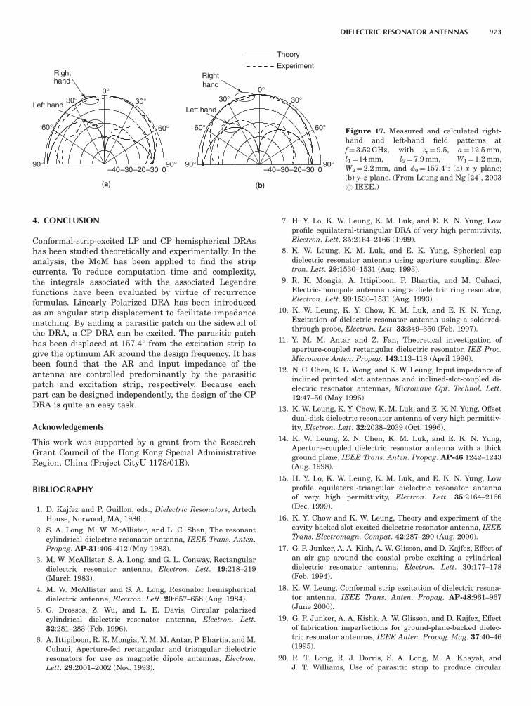
4. CONCLUSION
Conformal-strip-excited LP and CP hemispherical DRAshas been studied theoretically and experimentally. In theanalysis, the MoM has been applied to find the stripcurrents. To reduce computation time and complexity,the integrals associated with the associated Legendrefunctions have been evaluated by virtue of recurrenceformulas. Linearly Polarized DRA has been introducedas an angular strip displacement to facilitate impedancematching. By adding a parasitic patch on the sidewall ofthe DRA, a CP DRA can be excited. The parasitic patchhas been displaced at 157.41 from the excitation strip togive the optimum AR around the design frequency. It hasbeen found that the AR and input impedance of theantenna are controlled predominantly by the parasiticpatch and excitation strip, respectively. Because eachpart can be designed independently, the design of the CPDRA is quite an easy task.
Acknowledgements
This work was supported by a grant from the ResearchGrant Council of the Hong Kong Special AdministrativeRegion, China (Project CityU 1178/01E).
BIBLIOGRAPHY
1. D. Kajfez and P. Guillon, eds., Dielectric Resonators, ArtechHouse, Norwood, MA, 1986.
2. S. A. Long, M. W. McAllister, and L. C. Shen, The resonantcylindrical dielectric resonator antenna, IEEE Trans. Anten.Propag. AP-31:406–412 (May 1983).
3. M. W. McAllister, S. A. Long, and G. L. Conway, Rectangulardielectric resonator antenna, Electron. Lett. 19:218–219(March 1983).
4. M. W. McAllister and S. A. Long, Resonator hemisphericaldielectric antenna, Electron. Lett. 20:657–658 (Aug. 1984).
5. G. Drossos, Z. Wu, and L. E. Davis, Circular polarizedcylindrical dielectric resonator antenna, Electron. Lett.32:281–283 (Feb. 1996).
6. A. Ittipiboon, R. K. Mongia, Y. M. M. Antar, P. Bhartia, and M.Cuhaci, Aperture-fed rectangular and triangular dielectricresonators for use as magnetic dipole antennas, Electron.
Lett. 29:2001–2002 (Nov. 1993).
7. H. Y. Lo, K. W. Leung, K. M. Luk, and E. K. N. Yung, Lowprofile equilateral-triangular DRA of very high permittivity,Electron. Lett. 35:2164–2166 (1999).
8. K. W. Leung, K. M. Luk, and E. K. Yung, Spherical capdielectric resonator antenna using aperture coupling, Elec-
tron. Lett. 29:1530–1531 (Aug. 1993).
9. R. K. Mongia, A. Ittipiboon, P. Bhartia, and M. Cuhaci,Electric-monopole antenna using a dielectric ring resonator,Electron. Lett. 29:1530–1531 (Aug. 1993).
10. K. W. Leung, K. Y. Chow, K. M. Luk, and E. K. N. Yung,Excitation of dielectric resonator antenna using a soldered-through probe, Electron. Lett. 33:349–350 (Feb. 1997).
11. Y. M. M. Antar and Z. Fan, Theoretical investigation ofaperture-coupled rectangular dielectric resonator, IEE Proc.
Microwave Anten. Propag. 143:113–118 (April 1996).
12. N. C. Chen, K. L. Wong, and K. W. Leung, Input impedance ofinclined printed slot antennas and inclined-slot-coupled di-electric resonator antennas, Microwave Opt. Technol. Lett.12:47–50 (May 1996).
13. K. W. Leung, K. Y. Chow, K. M. Luk, and E. K. N. Yung, Offsetdual-disk dielectric resonator antenna of very high permittiv-ity, Electron. Lett. 32:2038–2039 (Oct. 1996).
14. K. W. Leung, Z. N. Chen, K. M. Luk, and E. K. N. Yung,Aperture-coupled dielectric resonator antenna with a thickground plane, IEEE Trans. Anten. Propag. AP-46:1242–1243(Aug. 1998).
15. H. Y. Lo, K. W. Leung, K. M. Luk, and E. K. N. Yung, Lowprofile equilateral-triangular dielectric resonator antennaof very high permittivity, Electron. Lett. 35:2164–2166(Dec. 1999).
16. K. Y. Chow and K. W. Leung, Theory and experiment of thecavity-backed slot-excited dielectric resonator antenna, IEEE
Trans. Electromagn. Compat. 42:287–290 (Aug. 2000).
17. G. P. Junker, A. A. Kish, A. W. Glisson, and D. Kajfez, Effect ofan air gap around the coaxial probe exciting a cylindricaldielectric resonator antenna, Electron. Lett. 30:177–178(Feb. 1994).
18. K. W. Leung, Conformal strip excitation of dielectric resona-tor antenna, IEEE Trans. Anten. Propag. AP-48:961–967(June 2000).
19. G. P. Junker, A. A. Kishk, A. W. Glisson, and D. Kajfez, Effectof fabrication imperfections for ground-plane-backed dielec-tric resonator antennas, IEEE Anten. Propag. Mag. 37:40–46(1995).
20. R. T. Long, R. J. Dorris, S. A. Long, M. A. Khayat, andJ. T. Williams, Use of parasitic strip to produce circular
(a) (b)
30°
60°
90°
0°30°
60°
90°
30°30°0°
60°60°
90°90°
Right hand
Left hand
Right hand
Left hand
Theory
Experiment
0–40–30–20–30 0–40–30–20–30
Figure 17. Measured and calculated right-hand and left-hand field patterns atf¼3.52 GHz, with er¼9.5, a¼12.5 mm,l1¼14 mm, l2¼7.9 mm, W1¼1.2 mm,W2¼2.2 mm, and f0¼157.41: (a) x–y plane;(b) y–z plane. (From Leung and Ng [24], 2003r IEEE.)
DIELECTRIC RESONATOR ANTENNAS 973
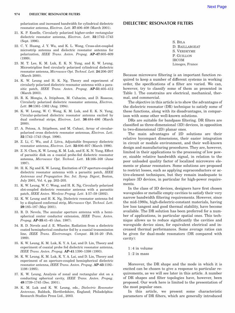
polarization and increased bandwidth for cylindrical dielectricresonator antenna, Electron. Lett. 37:406–408 (March 2001).
21. K. P. Esselle, Circularly polarized higher-order rectangulardielectric resonator antenna, Electron. Lett. 32:1742–1743(Sept. 1996).
22. C. Y. Huang, J. Y. Wu, and K. L. Wong, Cross-slot-coupledmicrostrip antenna and dielectric resonator antenna forpolarization, IEEE Trans. Anten. Propag. AP-47:605–609(1999).
23. M. T. Lee, K. M. Luk, E. K. N. Yung, and K. W. Leung,Microstripline feed circularly polarized cylindrical dielectricresonator antenna, Microwave Opt. Technol. Lett. 24:206–207(March 2000).
24. K. W. Leung and H. K. Ng, Theory and experiment ofcircularly polarized dielectric resonator antenna with a para-sitic patch, IEEE Trans. Anten. Propag. AP-51:405–412(March 2003).
25. R. K. Mongia, A. Ittipiboon, M. Cuhacim, and D. Rosecoe,Circularly polarized dielectric resonator antenna, Electron.Lett. 30:1361–1362 (Aug. 1994).
26. K. W. Leung, W. C. Wong, K. M. Luk, and E. K. N. Yung,Circular-polarised dielectric resonator antenna excited bydual conformal strips, Electron. Lett. 36:484–486 (March2000).
27. A. Petosa, A. Ittipiboon, and M. Cuhaci, Array of circular-polarised cross dielectric resonator antennas, Electron. Lett.32:1742–1743 (Sept. 1996).
28. Z. Li, C. Wu, and J. Litva, Adjustable frequency dielectricresonator antenna, Electron. Lett. 32:606–607 (March 1996).
29. Z. N. Chen, K. W. Leung, K. M. Luk, and E. K. N. Yung, Effectof parasitic disk on a coaxial probe-fed dielectric resonatorantenna, Microwave Opt. Technol. Lett. 15:166–168 (June1997).
30. H. K. Ng and K. W. Leung, Excitation of CP aperture-coupleddielectric resonator antenna with a parasitic patch, IEEE
Antennas and Propagation Soc. Int. Symp. Digest, Boston,July 2001, Vol. 4, pp. 202–205.
31. K. W. Leung, W. C. Wong, and H. K. Ng, Circularly polarizedslot-coupled dielectric resonator antenna with a parasiticpatch, IEEE Anten. Wireless Propag. Lett. 1:57–59 (2002).
32. K. W. Leung and H. K. Ng, Dielectric resonator antenna fedby a displaced conformal strip, Microwave Opt. Technol. Lett.29:185–187 (May 2001).
33. R. D. Nevels, The annular aperture antenna with a hemi-spherical center conductor extension, IEEE Trans. Anten.
Propag. AP-35:41–45 (Jan. 1987).
34. R. D. Nevels and J. E. Wheeler, Radiation from a dielectriccoated hemispherical conductor fed by a coaxial transmissionline, IEEE Trans. Electromagn. Compat. 31:16–20 (Feb.1989).
35. K. W. Leung, K. M. Luk, K. Y. A. Lai, and D. Lin, Theory andexperiment of coaxial probe fed dielectric resonator antenna,IEEE Trans. Anten. Propag. AP-41:1390–1398 (1993).
36. K. W. Leung, K. M. Luk, K. Y. A. Lai, and D. Lin, Theory andexperiment of an aperture-coupled hemispherical dielectricresonator antenna, IEEE Trans. Anten. Propag. AP-43:1192–1198 (1995).
37. K. W. Leung, Analysis of zonal and rectangular slot on aconducting spherical cavity, IEEE Trans. Anten. Propag.49:1739–1745 (Dec. 2001).
38. K. M. Luk and K. W. Leung, eds., Dielectric ResonatorAntennas, Baldock, Hertfordshire, England; Philadelphia:Research Studies Press Ltd., 2003.
DIELECTRIC RESONATOR FILTERS
S. BILA
D. BAILLARGEAT
S. VERDEYME
P. GUILLON
IRCOMLimoges, France
Because microwave filtering is an important function re-quired to keep a number of different systems in workingorder, the specifications of a filter are varied. We can,however, try to classify some of them as presented inTable 1. The constrains are electrical, mechanical, ther-mal, and commercial.
The objective in this article is to show the advantages ofthe dielectric resonator (DR) technique to satisfy some ofthese functions, along with its disadvantages, in compar-ison with some other well-known solutions.
DRs are suitable for bandpass filtering. DR filters areclassified as three-dimensional (3D) devices, in oppositionto two-dimensional (2D) planar ones.
The main advantages of 2D solutions are theirrelative bycompact dimensions, their easier integrationin circuit or module environment, and their well-knowndesign and manufacturing procedures. They are, however,limited in their applications to the processing of low pow-er, sizable relative bandwidth signal, in relation to thepoor unloaded quality factor of localized microwave ele-ments or planar resonators. Some solutions are proposedto restrict losses, such as applying supraconductors or ac-tive-element techniques, but they remain inadequate toreplace 3D devices, in particular for high-power require-ments.
In the class of 3D devices, designers have first chosenwaveguides or metallic empty cavities to satisfy their verynarrow bandwidth filtering requirements. However, sincethe mid-1980s, high-dielectric-constant materials, havinglow loss tangent and good thermal stability, have becomeavailable. The DR solution has been preferred for a num-ber of applications, in particular spatial ones. This tech-nique allows us to reduce significantly the cavities andwaveguide device sizes, for equivalent electrical and in-creased thermal performances. Some average ratios canbe given for dual-mode resonators (DR compared withcavity):
1 : 4 in volume
1 : 2 in mass
Moreover, the DR shape and the mode in which it isexcited can be chosen to give a response to particular re-quirements, as we will see later in this article. A numberof DR shapes and filter topologies have, however, beenproposed. Our work here is limited to the presentation ofthe most popular ones.
In this article, we present some characteristicparameters of DR filters, which are generally introduced
974 DIELECTRIC RESONATOR FILTERS
Next Page