device and circuit simulation of quantum electronic ...mazum/papers-mazum/50_rtdmodels… · ith...
TRANSCRIPT
IEEE TRANSACTIONS ON COMPUTER-AIDED DESIGN OF INTEGRATED CIRCUITS AND SYSTEMS, VOL. 14, NO. 6, JUNE 1995 653
Device and Circuit Simulation of Quantum Electronic Devices
S. Mohan, J. P. Sun, Pin& Mazumder, Member, IEEE, and G. I. Haddad, Fellow, IEEE
Abstract-Quantum electronic devices such as resonant tunnel- ing diodes and transistors are now beginning to be used in ultra- fast and compact circuit designs. These devices exhibit negative differential resistance (NDR) and/or negative transconductance in their I-V characteristics and have active dimensions of a few nanometers. Since the conventional drift-diffusion approximation is not valid for simulation of device behavior at this microscopic scale, quantum simulation models based on the Schriidinger equation are required to accurately predict the behavior of the device. However, these models are too slow for circuit simulation. This paper describes a modeling scheme that maintains the accuracy of the quantum simulation while achieving satisfac- tory speed for circuit simulation, and is applicable to a wide range of two and three terminal resonant tunneling devices and may also be extended to future scaled-down MOS and bipolar devices. A self-consistent solution of the Poisson and the Schriidinger equations for various bias points is used to build up tables of conductances, capacitances and other parameters. Table-lookup methods are then used during circuit simulation. Convergence techniques have been developed to overcome the problems caused by the NDR characteristics and the lookup-table model in simulation. While implementation details are presented for a resonant tunneling transistor (RTT), models for several other quantum electronic devices have also been implemented in NDR-SPICE.
I. INTRODUCTION
ITH silicon VLSI technology approaching the limits of scaling and miniaturization, new material systems
and device technologies are under investigation for improved speed and circuit compaction. Among the most promising of these are the resonant tunneling devices based on Gallium Arsenide (GaAs), Indium Phosphide (InP), and other 111-V semiconductor materials. The electrical performance of these devices is dominated by quantum effects. The devices contain quantum-well structures of nanometer dimensions comparable with the electron wavelength. Consequently, the wave nature of the electrons becomes important in determining the device electrical characteristics and these characteristics are very different from those of larger semiconductor devices such as the conventional MOSFET’s or bipolar transistors and the newer devices such as high electron mobility transistors (HEMT’s) or heterojunction bipolar transistors (HBT’s).
Manuscript received April 22, 1994; revised January 3, 1995. This work was supported in part by NSF under Grant ECS-9122166 and ARPA under Contract DAAH04-93-G-0242. This paper was recommended by Associate
Quantum electronic devices based on resonant tunneling (RT) through quantum-wellharrier structures exhibit negative differential resistance (NDR) and/or negative transconductance in their I-V characteristics [ 11. These characteristics have been used to build extremely compact or low-power digital circuits capable of operating at very high frequencies. Capasso et al. [ 11 described extremely compact implementations of multi- valued storage elements, frequency multipliers, analog-digital converters, and other applications of resonant tunneling de- vices. Chang et al. [2] describe a low-power logic family simi- lar to 12L using resonant tunneling diodes (RTD’s) and hetero- junction bipolar transistors (HBT’s). Imamura [3] describes a 1-b full-adder using just 7 resonant tunneling hot electron tran- sistors (RHET’s) and a few load resistors. Mohan et al. [4] de- scribe a self-latching, picosecond delay logic family using res- onant tunneling transistors (RTI”s) that provides compact im- plementations of the majority and latching functions. Seabaugh et al. [5] describe a nine-state memory using a single multi- peak RTD, while Wei and Lin [6] describe a novel analog to digital converter using RTD’s to reduce the number of ele- ments required for a flash type converter from 0(2n) to O(n).
Load lines and approximate equations may be used to design small circuits using passive elements and a few conventional active elements, such as FET’s or BJT’s. However, the design of more complex circuits and of circuits designed to meet strict specifications on voltage/current levels and fanouts requires the use of a good circuit simulator to accurately analyze the performance of the circuit before it is built. The basis for accurate circuit simulation is the circuit model for the device under consideration. Modeling of RlT’s for circuit simulation is a new field; earlier work had focussed primarily on the relatively slower but more accurate modeling for device simulation where the goal is to design a new device with desired properties. This paper presents a device model for resonant tunneling transistors and the incorporation of the device modeling data into a much simpler circuit simulation model. This model has been implemented in SPICE along with new ideas to aid in the convergence of the simulation. The two main contributions of the present work are the incorporation of device modeling data into circuit simulation models and the enhancement of the simulation algorithms to improve convergence in situations where the NDR and piecewise linear characteristics of the devices cause the simulation to oscillate when the actual circuit is perfectly stable. These techniques _ _
Editor S. G. Duvall.
puter Science, University of Michigan, Ann Arbor, MI 48109 USA.
may also be applied to the Simulation of other devices where quantum effects may come into play, such as future scaled- down MOS or bipolar transistors.
The authors are with the Department of Electrical Engineering and Com-
IEEE Log Number 9410371.
02784070/95$04.00 0 1995 IEEE
A. Device Modeling The conceptual framework of device modeling can be
identified to fall into three levels, i.e., the drift-diffusion mod- els, the Boltzmann transport models, and quantum transport models. If quantum effects are neglected, quantum transport models can reduce to the Boltzmann transport models, while the latter may further reduce to the drift-diffusion models if transient and hot electron effects are neglected. In each of the transport models, the corresponding carrier transport equations are solved within its physical framework and its approximations. Conventional transistors are simulated using the drift-diffusion model, but quantum electronic devices such as the RTD’s and R W s require the self-consistent solution of the Poisson and the Schrodinger equations [7]. These models are computationally expensive and their applicability is usually limited to single-device simulation.
B. A New Modeling Framework for RT Devices Previous work on circuit modeling for RT devices has
been limited to RTD’s [8] and quantum modeling has been too complex and slow for circuit simulation. This paper presents a new framework for RT device modeling where a complex quantum model of the device is used to extract circuit parameters such as conductances, transconductances and bias-dependent capacitances, which are then used to build a tabular model for circuit simulation. In addition, the convergence properties of the simulation program are studied and convergence problems caused by the NDR characteristic are identified and resolved by the development and implemen- tation of new convergence algorithms. The following sections describe the quantum modeling of an RTT, the extraction of circuit parameters and the circuit model, the convergence problems caused by the NDR characteristic and the solution, and finally a few sample circuits simulated using the new models. The new modeling framework makes it relatively easy to substitute measured data for the data from quantum simulation. While the R l T model has been implemented based on data from quantum simulation, models for other RT devices such as RTD’s and RHET’s have been developed based purely on measured values [9].
11. QUANTUM MODELING OF RESONANT TUNNELING DEVICES Various quantum mechanical models have been attempted
in modeling quantum devices, such as the kinetic quantum model based on the Wigner function description of electron ensemble, the envelope function model based on the envelope function description of electron states, and more microscopic models based on the empirical tight-binding or pseudopotential calculations.
We now envision a quantum device structure consisting of a quantum barrierlquantum-well region and two or more heavily doped contact regions. The main goal of the modeling calculations is to obtain the device dc Z-V and small signal C-V characteristics by solving the electron transport equations. In the envelope function approach, the transport is initiated by sending eigenstate electrons from device contacts into a device structure. The electrons, bearing variable effective mass
CV and G V W.W
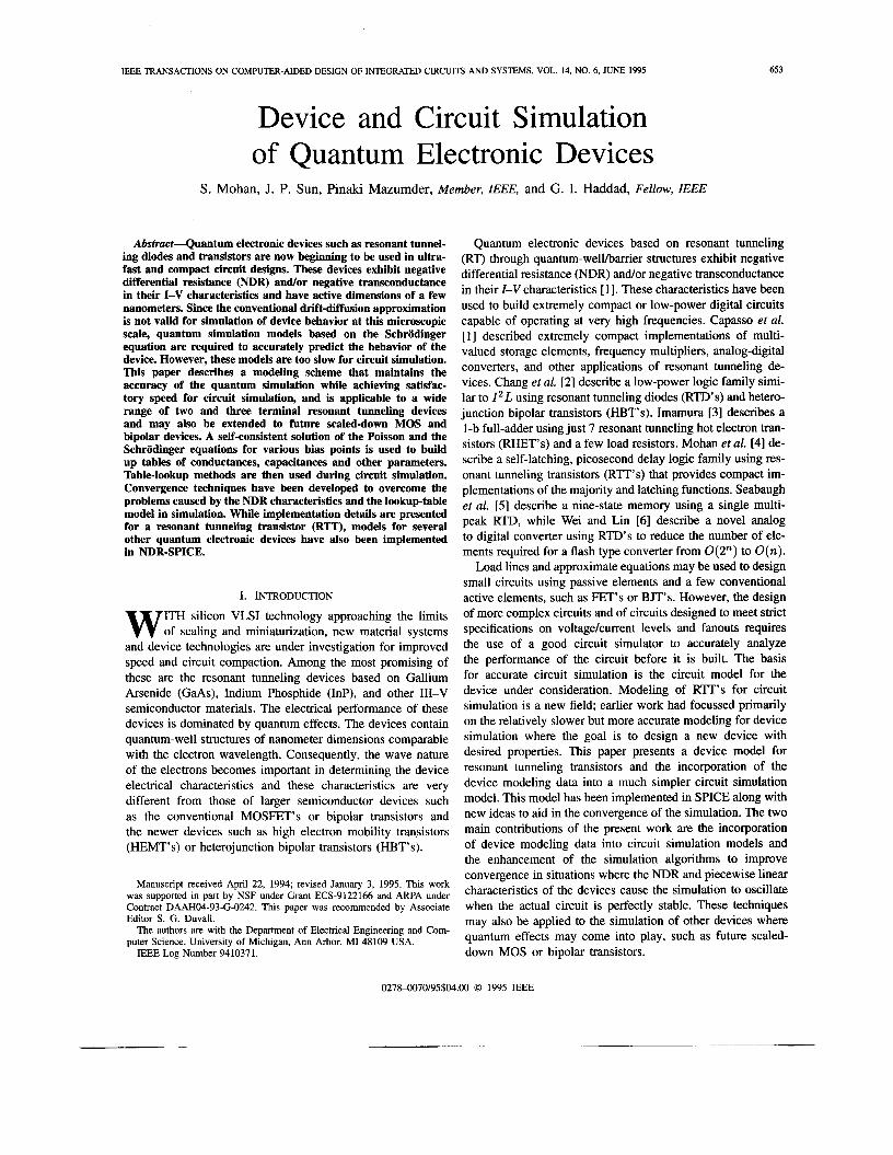
Fig. 1. under study.
Self-consistent solution procedure in modeling the quantum devices
in a layered structure, interact with the space-dependent device potential via the Schrodinger equation. Accurate determination of the electron potential profile in a given device structure is therefore critical for the calculation of electron wavefunctions. Once the wavefunctions are obtained, charge, and current densities can be readily calculated.
The Poisson equation relates the electrostatic potential to the charge distribution, in which fixed charge distribution represents ionized impurities (doping profile of the device) and mobile charge distribution represents electron transfer (space charge effects). Since the carrier density responds to the same electrostatic potential it generates, we have a self- consistent problem which entails simultaneous solution of the Schrodinger equation and the Poisson equation. Additional treatment must also be considered for charge in the quantum well(s) to account for the quantized effects, which will be referred to as quantum well calculation. The solution of the Schrijdinger equation and the Poisson equation gives self- consistent potential and charge distributions across the device.
When a device is in operation, electrons are injected from the contacts by external electric fields, and the device is driven away from equilibrium. Energy and particle exchanges take place and the device system is open to its environment. This sets up the boundary conditions for the current carrying electron waves in the device model. The incident eigenstate electrons traverse through the device while being scattered by the device potential profile. Other scattering processes can also be considered in this calculation. This traveling wave calcula- tion under applied bias voltages requires steady-state solution of the time-independent Schrodinger equation which gives device Z-V characteristics. The applied bias also modifies the space charge and potential distributions. With the knowledge of these distributions under various bias conditions, the device C-V characteristics can be evaluated. Fig. 1 summarizes the general solution procedure outlined above.

MOHAN et al.: DEVICE AND CIRCUIT SIMULATION OF QUANTUM ELECTRONIC DEVICES
a t t e r Contact
e Contact Etch Stop
n+ Oak3 Eoitter
iAu.
n+ 0.A. Collector
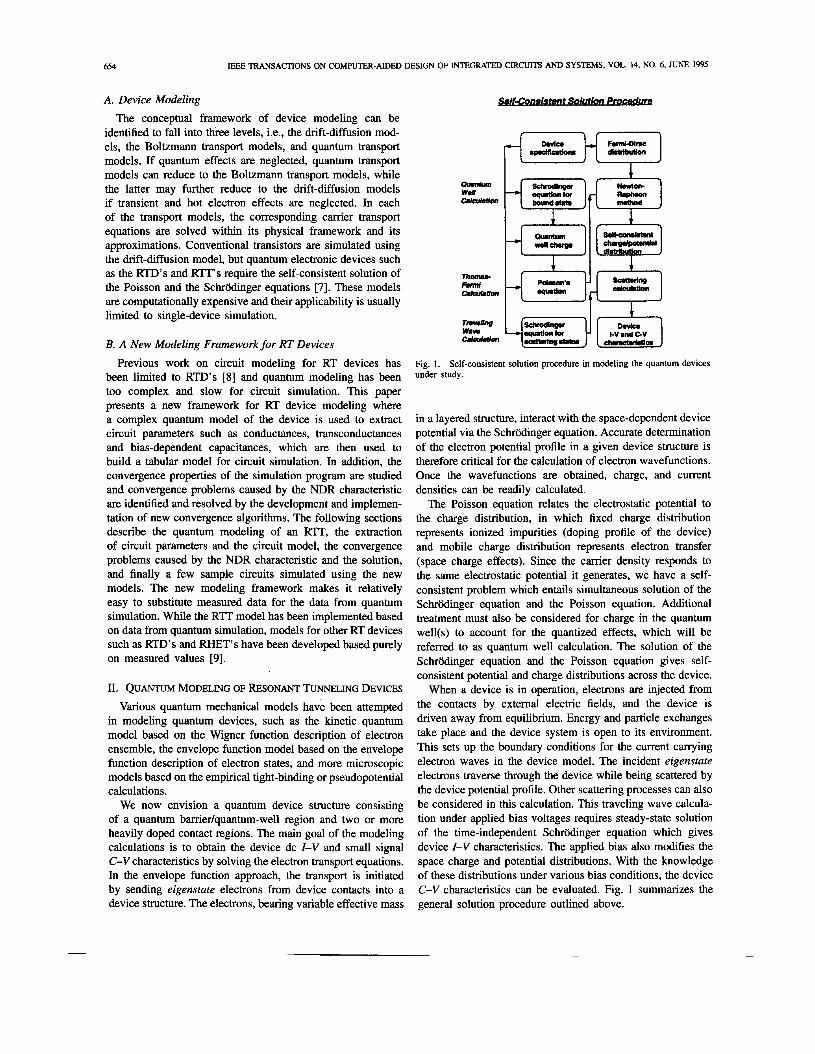
Fig. 2. BSR'IT structure and conduction band profile.
The self-consistent calculations for the device models can be divided into three parts and are referred to as the Thomas-Fermi calculation for the self-consistent potential, the quantum-well calculation for space charge in the quantum well(s), and the traveling wave calculation for current density, as shown in Fig. 1. Readers are referred to [lo] for more details.
A. Self-consistent Model of the R T s A variety of R'IT's, all based on the resonant tunneling
mechanism but with different operating principles, has been proposed and demonstrated. Regardless of the particular type of R'IT (unipolar, bipolar, field effect, hot electron, or bound state), the transistor action is based on the interaction between the incident electrons and subbands in the quantum well, with the position of the subbands with respect to the emitter Fermi level modulated by the base andor collector biasing or channel gating. These devices typically present negative differential resistance for a fixed emitter-base bias and nega- tive transconductance for a fixed collector-emitter bias, with multiple current peaks for some R'IT variations.
A particular version of the R'IT's, also known as the Bound State Resonant Tunneling Transistor (BSRTT), was proposed by Haddad er al. [ 111 at the University of Michigan and Schulman er al. [12], independently. A typical BSR'IT conduction band structure, which is used for modeling the JC-VCE characteristics, is shown in Fig. 2. This transistor structure, as proposed by Haddad er al., [ l l ] utilizes a base material with lower band gap than the contact layers. Bound states are created in the narrow quantum-well base. Electrons in these bound states form a low-resistance base region for application of bias to the device. Since these electrons are bound, they will not contribute appreciably to perpendicular base current flow other than for the displacement current between emitter and collector. Current flow is due to tunneling via the second resonant energy level in the well, while the base particle current is due to electron scattering in the quantum-well base. The structure was proposed to alleviate the problem of high base resistance in conventional RlT's.
In addition, an extended barrier is placed in the collector region to reduce the leakage current tunneling from the base region to the collector through the base-collector thin bar- rier in the conventional RTT's. The extended barrier affords additional advantages besides reducing the leakage current. The base-collector capacitance is significantly reduced, so that displacement currents accompanying bias changes across this junction are suppressed. Also, since punch-through from the base to the collector is less likely to occur, the base contact is easier to accomplish. Both theoretical and experimental work on the BSR'IT has been conducted [13], [14] and we will, in this section, discuss the self-consistent effect on the device I-V characteristics.
The device structure (Fig. 2) to be modeled consists of a double-barrier quantum well (DBQW) and a flat extended barrier of 0.125 eV. The quantum-well base is 80 a thick and doped at 2 x 1Ol8 ~ m - ~ .
To understand the device operation, one needs to study the relative motion of the Fermi level at the emitter, EFE, the bound state levels (especially the second quasibound state E2) in the quantum-well base, and the top of the extended barrier Eext under various bias conditions. In addition, under sufficient bias thermionic emission and tunneling via the top of the barriers may become dominant in the overall current transport. The resultant current density and the I-V characteristics depend on the interplay among these combined effects.
We first examine the JC-VBE characteristic of the BSR'IT structure based on the self-consistent calculation (see Fig. 1). When bias is applied, &E. the electron Fermi level in the emitter, Ea, the resonant level (bound state) in the base and Eext, the extended barrier level (see Fig. 2) move in accordance with the changes in VBE and VCE. At a fixed VCE, EFE moves upwards and E2 moves downwards when VBE increases. Keeping track of the positions of the bound states with the bias change indicates that E2 becomes 36.90 meV, close to EFE, at VBE = 0.19 V, and 18.30 meV at 0.26 V. Further increase of VBE will lift E2 off from the well. This is because the top of the collector barrier at this bias is reduced

656 IEEE TRANSACTIONS ON COMPUTER-AIDED DESIGN OF INTEGRATED CIRCUITS AND SYSTEMS, VOL. 14, NO. 6, JUNE 1995
" 8 I I I 0.0 0.1 O h 0.3 0.4 0.5
Vbe(V)
Fig. 3. structure obtained from self-consistentcalculation.
Collector current density J c as a function of VBE for the BSRTT
IC
0.00 O S 1.00 1.50 zoo 2.50 3.00
Vce VOLTS
Fig. 4. Collector current IC as a function of VcEfor the BSR'IT calculated with self-consistency.
to 0.2184 eV as seen by inspecting the potential profile which is unable to support a second bound state. If we plot the current as a function of VBE, a current peak would be expected corresponding to the alignment between EFE and E2 at around 0.19 V, and a decrease in current beyond that voltage because there is no resonant state available in the well. The current will increase again with increasing VBE due to the thermionic emission and tunneling via the tops of the barriers. A consistent observation is found in Fig. 3, where the calculated JC is plotted as a function of VBE for the BSRTT structure.
Next we study the JC-VCE characteristics of the BSRTT cal- culated with self-consistency. The inclusion of self-consistency in the device modeling has revealed strong feedback effects in the narrow quantum-well base transistor. In the device model without self-consistency, it was assumed that for a fixed VBE, a change in VCE does not produce any modifications to the emitter-base potential profile, and hence no changes occur for
if the bound state charge in the base is not sufficient to keep the base at equilibrium. Since the base does not behave as a perfect shield, at sufficiently large collector bias, further increase in the collector bias will have an appreciable feedback from the output port to the input port, including the base region. The bound states in the quantum well will shift in energy due to the changes in the emitter-base potential profile; the actual emitter- base potential difference may deviate from its nominal value set by VBE. These effects are likely to cause the device to be off resonance and the collector current will drop significantly, leading to the NDR in the BSRTT's.
The calculated IC versus VCE characteristics of the RTT, with self-consistency, are shown in Fig. 4. These charac- teristics have also been observed in device measurements [ 141. Calculations without self-consistency, on the other hand, would have produced IC versus VCE characteristics similar to conventional BJT characteristics, contradicting the observed characteristics of this device.
III. INCORPORATION OF THE RTT MODEL IN SPICE
In constructing a circuit model for RTT's, it is assumed that the electron transport follows small changes in applied voltage/current in a quasistatic manner, and hence the circuit elements in the model can be approximately evaluated using the model calculation with the time-independent Schriidinger equation. This assumption implies that the circuit model may be valid up to a certain high frequency range. Further increase in frequency may require device simulation in the time domain. As outlined above, the collector current (density) is calculated as a function of both VBE and VCE. Similarly, the charge/capacitance is calculated as a function of the base, emitter and collector voltages, based on the quantum modeling scheme outlined in Fig. 1.
In the present circuit model, the RTT is considered to be a voltage-controlled current source. Rg is the base resistance which accounts for the charging and discharging effects of the capacitance between the emitter and base. The current transport in the circuit model is represented by the voltage- controlled current source gmV&, and the collector resistance Rc. In the following discussion the collector resistance is represented as an equivalent conductance gce = 1/Rc
As discussed in the above section, since the BSRTT operates based on the bound state charge and second resonant level in the base, gm may be negative for certain bias ranges. Given a table of current values IC as a function of the voltages VBE and VCE, the values gm and gce are tabulated based on the above definition For the large signal circuit model, both gm and gce are functi )ns of VBE and VCE. Hence the change in collector current for a small change in base and collector voltages may be represented as
the bound state levels in the base. This assumption is not valid SIC = gm . SVBE + gce . SVCE. (3)

MOHAN et al.: DEVICE AND CIRCUIT SIMULATION OF QUANTUM ELECTRONIC DEVICES 651
I I 4 E
Fig. 5. A large signal circuit model of the BSRIT.
(a) (b)
Fig. 6. Convergence of NDR circuits depends on the initial guess. (a) Con- vergence of Newton-Raphson iterations for general function. @) Oscillations in Newton-Raphson iterations for NDR circuit with wrong initial guess and convergence with right initial guess.
However, in actual circuit operation, the operating point of a circuit may abruptly shift from one positive differential resis- tance region of the IC-VCE curve to the other, corresponding to a large change in VCE. When 6 V c ~ is large, the above equation for calculating the current is no longer valid, since the error is large. Hence IC is calculated directly from the given values of VBE and VCE, this calculation being somewhat more tedious than the quick calculation of 61c from the above equation. However, the gm and gce values are still required in the computation of the Jacobian used in the basic circuit equation solved in each iteration of the simulation algorithm [15]. When abrupt discontinuities in the device current or voltage are seen, special convergence algorithms, described below, are used to force the simulation to converge to the correct state.
The capacitances in the circuit model are defined as
where QBE and QBC are the charge between the emitter and base, and the base and collector, respectively. Changes of the charge at both sides of the barriers and the bound state with bias are calculated to give the values of the capacitance. The contact resistances and the electrode resistance are not considered in this device intrinsic model (see Fig. 5) . Note that although this circuit model for R'IT's resembles the hybrid- R model for BJT's, the circuit elements in the model now represent very different mechanisms of the transistor operation and are calculated based on a quantum model.
Tabulated values for IC as a function of VCE and VBE are obtained from device simulation, as are values for the capacitances. These tables are read by the initial setup rou- tines of the new NDR model implemented in SPICE. The
Volts
Fig. 7. RTT circuit and load line used in convergence experiment.
conductance and transconductance values are calculated from the current table and stored in separate tables so that they do not have to be recomputed each time during simula- tion. With the implementation of the table-lookup current source/transconductance model, the complete model described above may be incorporated into the device routines, where the nodal equations for the elements are formulated. The details of nodal equation formulation for passive elements and controlled source, and simulation are described adequately in the literature (see for example [16] and [15]) and will not be discussed here. The new element here is the table driven current source/transconductance. Given the values of VBE and VCE, the values of current, conductance and transconduc- tance are obtained by linear interpolation from the tables and addedfsubtracted from the corresponding LHS/RHS nodes in the equation formulation step of SPICE [15].
A. Convergence Problems Due to the NDR Characteristic SPICE uses Newton-Raphson iterations to solve nonlinear
circuit equations. Newton-Raphson iterations are guaranteed to converge when the initial guess is close to the actual root of the equation. Consider for example, a simple circuit consisting of a voltage source, a resistor and an R l T in series (see Fig. 7). Let the base voltage of the RTT be held constant so that the current through the RTT is described by i = g(w) where the function g describes the NDR characteristic. Then the nodal equations for the circuit can be written in the form f ( V ) = 0, where f ( V ) is a nonlinear function of the voltage vector V. In the case of the simple circuit above, the circuit may be described by a single scalar equation f(v) = 0, where v is the voltage across the RTT and f ( w ) has the form shown in Fig. 6(b). When the Newton-Raphson method is used to find the root of the nonlinear equation, the choice of a correct initial guess is crucial in determining the solution obtained by the algorithm. Fig. 6(a) shows a typical function of one variable x and shows the progress of the Newton-Raphson iterations starting from an initial value of x0 and converging to the root of the function g(x). Fig. 6(b) shows a typical function f(x) associated with NDR circuits. The function f(x) may, for instance, represent the total collector current through an RTT and a series load resistor. When the initial guess for Newton- Raphson iterations is x0, successive iterations produce the

658 IEEE TRANSACTIONS ON COMPUTER-AIDED DESIGN OF INTEGRATED CIRCUITS AND SYSTEMS, VOL. 14, NO. 6, JUNE 1995
following sequence 20, 21, 22, 21, 2 2 , .e.. This oscillation is a direct consequence of the shape of the function and the initial starting point. If the initial guess were moved to 20’ the solution quickly converges to Xf, the root of f(2). Hence the choice of the initial guess is crucial in determining the convergentloscillatory behavior of the simulator.
For dc simulations using SPICE, a good initial guess can be specified by the user. However, for dc transfer curve or transient simulation, SPICE automatically takes the solution from the previous simulation point (previous bias point for dc transfer curve or previous time point for transient analysis) as the initial guess for the solution at the current point. Referring to the example of the circuit described earlier, the previous simulation point could have had a smaller applied voltage, leading to a solution at $0 in Fig. 6. The new simulation point has a larger applied voltage and a single solution point Xf. But the wrong initial guess due to the previous operating point causes the simulation to oscillate.
SPICE employs several techniques to aid convergence [17]. Gmin stepping changes the value of the minimum conductance between nodes; source stepping reduces all voltage sources to 0 and then slowly steps them up to the actual value; device limiting prevents the voltages and currents of devices with exponential characteristics, such as p-n junctions from going out of range. However, none of these techniques is of use in the simple example shown in Fig. 6(b), if the initial guess is 20. Changing the value of gmin does nothing to affect this particular problem. Reducing sources to 0 and then stepping them up, still produces the same initial guess 20 in some cases. In some other cases involving dc analysis convergence is produced as follows. Assume the RTT in the simple resistive load circuit has two stable points at the previous simulation point and exactly one stable point corresponding to the second positive differential resistance region at the current simulation point. If the previous simulation had found the stable point in the first positive differential resistance region as the solution point, the dc simulation for the current point (obtained by increasing the supply voltage) oscillates, since there is a big jump in the operating point over an NDR region. If the RTT characteristics are such that there is just one stable point for small values of VBE and VCE, corresponding to the second PDR region, this solution point provides a good starting point for future source stepping iterations where both the input and supply voltage are increased simultaneously and the iterations converge to the right solution. Hence source-stepping is not guaranteed to force convergence. Device limiting is not applicable here. The only trick that can force convergence to the right solution is the choice of 20’ as the initial solution, but there is no existing routine in SPICE to do this. The reason for this limitation in SPICE is that the none of the basic devices such as BJT’s, FET’s and passive elements which are modeled in SPICE have a folded I-V or NDR characteristic.
Hence the following algorithm was implemented to identify oscillatory conditions in simulation (i.e., the simulation does not converge even when the circuit itself is not oscillatory) for the RT elements in the circuit and force convergence. The Ic-V& characteristic of an RTT for a fixed V& is split into three regions-the initial region of positive differential
resistance, the negative differential resistance region, and the second region of positive differential resistance. Within each region, the characteristic is represented by one or more piece- wise linear segments, depending on the number of data points obtained from quantum simulation or device measurements.
CONVERGENCE ALGORITHM FOR MULTI-SEGMENT PIECEWISE LINEAR NDR CURVE <preprocessing>
read table of current values tabulate conductance and transconductance values
at each time point, for each RTT <simulation>
find the direction of change of VCE update LL = (D, L) = direction and
length of longest monotonic run of changes in VCE
store LL in the state vector of the device
if (timestep < k*DELMIN) or if other convergence routines
have failed CALL force routine /* DELMIN is the minimum time step and k is a constant. The time step is repeatedly reduced when there is no convergence. If the time step equals DELMIN, the simulation is aborted. Else, when convergence is reached, the time step is increased at each time point so long as it is smaller than the maximum time step allowed. */
CONVERGENCE ALGORITHM: THE FORCE ROUTINE if the device VCE is oscillating then
if LL has direction D = INCREASING max = highest V& in the oscillation imax = index of max in the gce table iforce = smallest index > imax
such that gce[index] >= 0 use iforce instead of VCE to calculate
current, gce and gm else if LL has direction D = DECREASING
min = smallest VCE in the oscillation imin = index of min in the gce table iforce = biggest index < imin
such that gce[index] >= 0 use iforce instead of VCE to calculate
current, gce and gm Fig. 7 shows the RTT circuit and loadline used to demon-
strate the convergence problem and the solution. The base voltage of the RTT is held constant while the supply voltage is first ramped up and then ramped down. As the supply voltage is ramped up, the voltage at the OUT node increases from

MOHAN et al.: DEVICE AND CIRCUIT SIMULATION OF QUANTUM ELECTRONIC DEVICES 659
I
Fig. 8. Output voltage and time as a function of iteration number for Rl'Tkesistor circuit.
I I 0 5 IS 20 25
I.nlon 1-100 IO
Fig. 9. Closeup of output voltage, showing oscillation.
0 to the point labeled 1 on the R'IT characteristic. A slight increase in V,, then causes the operating point to jump to 2. However, when SPICE uses the point 1 as the starting point for Newton-Raphson iterations when the solution is at point 2, the algorithm fails to converge. This is illustrated in Figs. 8 and 9. Fig. 8 shows the output voltage and time as a function of the iteration number. It can be seen that the timestep becomes very small, starting at around iteration 50 and the time hardly increases until almost iteration 150. The output voltage is also constant in this figure, up to iteration 120 or so. When viewed at a higher magnification in 9, it can be seen that the voltage is actually oscillating until iteration 1 18 when the convergence algorithm forces convergence to point 2. Hence the voltage jumps to approximately 1.7 V and the time step starts increasing. However, until iteration 150, approximately, the time step is still so small that the output voltage and time appear to be almost constant in Fig, 8. A similar pattern of oscillation followed by forced convergence is seen when the supply voltage VCC is ramped down and the output voltage jumps from point 3 to point 4. It may be noted here that the points 1 . . .4 in Fig. 7 are only symbolic and do not represent the actual voltages and currents in Figs. 8 and 9.
0 0 2 0.4 a8
Tmn
(b)
Fig. 10. Self-latching majority gate. (a) Circuit. (b) Simulation results.
It may be noted here that the new convergence routines apply only to the specific resonant tunneling devices that are causing the simulation algorithm to oscillate. The basic SPICE algorithms for solving nonlinear equations have not been modified. The new convergence routines are analogous to the device limitingkonvergence methods applied to spe- cific conventional devices such as diodes or bipolar junction transistors [15], and are part of the device modeling routines rather than the main simulation program. Hence the behavior of the SPICE program when simulating other devices is not adversely affected by the new device model and convergence algorithms.
B. Simulation of Large Circuits Using rhe RIT Model
The implementation of the large signal R'IT model and convergence algorithms has allowed fairly large R'IT circuits to be designed and simulated. In particular, a complete set of basic logic gates was designed using R'IT's [4] and an adder circuit containing 10 s of R'IT's was simulated 1181. Fig. 1O(a) shows a circuit containing just 3 R'IT's that implements the Majority or Carry function [4]. Whenever two or more of the inputs are at logic 1, the output is at logic 1; otherwise the output is at logic 0. However the added attraction of this circuit is that it is self-latching and the output does not change until a clock signal is applied, as seen in Fig. 10(b). The self- latching feature of this logic family implies that maximally pipelined circuits with each level of logic corresponding to a pipeline stage, can be designed without incurring the area or

660 E E E TRANSACTIONS ON COMPUTER-AIDED DESIGN OF INTEGRATED CIRCUITS AND SYSTEMS, VOL. 14, NO. 6, JUNE 1995
inverters1 I 2
I I
I
I v ;
15 1862
Fig. 11. Pipelined adder circuit using RTTs.
a o.POj 1-1 b m
0.64
344064
1.00~49 0.W . . . . 0.24 . , . . 0.48 . . . . 0.71 . , , . 0.95
Fig. 12. output; higher voltage level of signals corresponds to logic 0.
1-b adder SPICE output showing inputs a, b, cin, clocks, and sum
10.750
time penalty of extra pipeline latches. This pipelining scheme has been called nanopipelining [ 181. Fig. 1 1, a pipelined adder circuit containing 39 R W s was designed with the help of the simulator, and Fig. 12 shows the simulation output for this circuit. It was shown in [18] that four such adders, with a ripple carry scheme, along with a buffering and feedback scheme for the carry out of the last bit, could achieve a throughput of 1 32-b addition every 1.5 ns.
Table I shows the simulation time and the data memory required, for several different RTT circuits. All measurements were made with NDR-SPICE running on a Sun SPARCstation 1 machine with 16 Mbytes of memory, with a 20 MHz CPU and FF’U, benchmarked at 1.4 M flops [19]. The circuit shown in Fig. 10(a) is called ‘trubist3’ in the table, and the RTT count includes one RTT in the level shifter. The ‘other device’ counts for all circuits in the table include the capacitors and resistors from the RTT model. The ‘time pts’ column in the table is just the simulation time divided by the maximum allowed time step for the simulation algorithm. The time
SUM
TABLE I SIMULATION TIME AND MEMORY FOR R’IT CIRCUITS
trubist3 trubist4 combN 2level 3level and 12 sum 22 or3 36
26 27 33 33 75 93 75
124 198 279
1200 950
1050 950
1300 500 200
1200 600
1650 -
352256 360448 360448 368640 405504 425984 405504 491520 548864 888832 -
13.190 9.030
12.240 12.020 49.890 26.750 5.960
57.090 51.580
298.290
step is dynamically adjusted to ensure accuracy and maintain simulation speed. Hence this is a lower bound on the number of simulation time points. The large circuit shown in Fig. 11 appears as ‘comblN’ in the table. The device counts there are somewhat higher due to the addition of some buffer circuitry. The simulation time is a function of the circuit complexity and the number of simulation time points. Sharp discontinuities in node voltage/current waveforms cause the simulator to reduce the time step, i.e., increase the number of time points, in order to maintain accuracy. In all except the last example, the total run-time is less than a minute, for circuits containing as many as 36 RTT’s. In contrast, the quantum simulation of a single R l T to obtain the device characteristics takes two days on a similar machine. Hence the table-driven model is orders of magnitude faster than the quantum model, and is fast enough to be used in circuit simulation.
While the technology for fabricating 3-terminal RTT’s is still not sufficiently advanced to build the circuits described above, it is possible to verify the operating principles of these circuits using the simpler RTD’s in conjunction with bipolar transistors. RTD’s are two terminal devices with the

MOHAN et al.: DEVICE AND CIRCUIT SIMULATION OF QUANTUM ELECTRONIC DEVICES 66 1
VCC I
I‘; I tK
V
10 2 0 30 40
us time
Fig. 13. RTD + bipolar transistor circuit showing simulation results and oscilloscope traces.
same double barrier structure as the RTT’s but without the base contact and the collector barrier. The RTD exhibits NDR characteristics corresponding to just one of the curves shown in Fig. 4. Hence the RTD may be simulated using the R l T model, with the base voltage held constant. The same convergence problems associated with the circuit of Fig. 7 are observed when the RTT with the fixed base voltage is replaced by an RTD. Several RTD+bipolar transistor circuits have been successfully simulated and built, verifying the accuracy of the simulation model and the efficacy of the convergence algorithms. An example RTD+bipolar circuit is shown in Fig. 13, along with the simulation results and the oscilloscope traces. Several other examples may be seen in [20].
IV. CONCLUSION
The quantum device modeling scheme described here has been applied to RTT’s and RTD’s and is now being applied to RHET’S. The table-driven approach using simulated values from the quantum device model has allowed the simulation of circuits using new devices leading to a very short time lag between the fabrication of a new device and the design of circuits using these devices. The link between device simula- tion and circuit simulation established here, has allowed circuit designers to design circuits with a high degree of confidence even before the device is fabricated and to quickly optimize the design as soon as device measurements are available. This method may readily be extended to the circuit simulation of future scaled down MOS and bipolar transistors, where tables derived from quantum modeling can be augmented with convergence algorithms for fast and accurate circuit simulation.
A modeling scheme for quantum electronic devices that encompasses both quantum modeling results and measured I-V characteristics of resonant tunneling devices has been developed. This SCheme has been used in developing and im- plementing models for R’IT’s, RTD’s, RHET’s, and MRTD’s in NDR-SPICE, an enhanced version of spice-je that contains
REFERENCES
[i] F. Capasso, s. Sen, F. Beltram, L. M. Lunardi, A. s. Vengurlekar, P. R. Smith, N. J. Shah, R. J. Malik, and A. Y. Cho, “Quantum functional devices: Resonant-tunneling transistors, circuits with reduced complexity and multiple-valued logic,” IEEE Trans. Electron Devices,
new convergence routines to force the simulator to converge vol. 36, pp. 2065-2082, Oct. 1989. to the right solution for circuits containing the new NDR [2] C. E. Chang, P. M. Asbeck, K.-C. Wang, and E. R. Brown, “Analysis devices. ~ R - S P I C E has been used to circuit designs of heterojunction bipolar transistor/resonant tunneling diode logic for
low-power and high-speed digital applications,” IEEE Trans. Electron
131 K. Imamura, “Full adder uses RHET’S,” J. Electron. Eng., vol. 28, pp.
using RTT’s, RTD’s and other supported devices. Reference Devices, vol. pp, 685491, 1993, [41 d e ~ r i b e s two new logic families using Rn’S, designed . .
and simulated with the helD of the R l T models described 76-80, 90, Nov. 1991.
above, implemented in NDR-SpICE and [20] describes new multiple-valued logic circuits designed using RTD’s, RHET’s
[41 S. Mohm, P. Mazumder, R. K. Mains, J. P. Sun, and G. I. Haddad, “Logic design based on negative differential resistance characteristics of auantum electronic devices.” IrEE Proc.-G. vol. 140. OD. 383-391.
and RTBT’s and simulated with NDR-SPICE. Dec.. 1993.

662 IEEE TRANSACTIONS ON COMPUTER-AIDED DESIGN OF INTEGRATED CIRCUITS AND SYSTEMS, VOL. 14, NO. 6, JUNE 1995
t51
171
181
[91
1141
A. C. Seabaugh, Y.-C. Kao, and H.-T. Yuan, “Nine-state resonant tunneling diode memory,” ZEEE Electron Device Lett., vol. 13, pp. 479-481, Sept. 1992. S.-J. Wei and H. C. Lin, “Multivalued SRAM cell using resonant tunneling diodes,” ZEEE J. Solid-State Circuirs, vol. 27, pp. 212-216, Feb. 1992. S . Datta, Quantum Phenomena, vol. VIII of Modular Series on Solid State Devices. Reading, M A Addison-Wesley, 1989. T.-H. Kuo, H. C. Lin, U. Anandakrishnan, R. C. Potter, and D. Shupe, “Large-signal resonant tunneling diode model for spice3 simulation,” in Znt. Electron Devices Meeting Tech. Dig, 1989, pp. 567-570. P. Mazumder, J. P. Sun, S. Mohan, and G. I. Haddad, “DC and transient simulation of resonant tunneling devices in NDR-SPICE,” in 2Zst Znt. Symp. Compound Semiconductors, 1994. I. P. Sun, “Modeling of semiconductor quantum devices and its appli- cations,’’ Ph.D. dissertation, Dep. of EECS, Univ. of Michigan, Ann Arbor, 1993. G. I. Haddad, R. K. Mains, U. K. Reddy, and J. R. East, “A pro- posed narrow band-gap base transistor structure,” Superlattices and Microstructures, vol. 5 , no. 3, pp. 437441, 1989. J. N. Schulman and M. Waldner, “Analysis of second level resonant tunneling diodes and transistors,” J. Appl. Phys., vol. 63, pp. 2859-2861, 1988. G. I. Haddad, U. K. Reddy, J. P. Sun, and R. K. Mains, ‘The bound-state resonant tunneling transistor (BSRTT): Fabrication, D.C. I-V characteristics and high-frequency properties,” Superlattices and Microstructures, vol. 7, no. 4, p. 369, 1990. W. L. Chen, G. I. Haddad, G. 0. Munns, and J. R. East, “Experimental realization of the bound state resonant tunneling transistor,” in 5Zst Annual Device Res. Con$, 1993. W. J. McCalla, Fundamentals of Computer-Aided Circuit Simulation. Norwell, MA: Kluwer, 1988. L. 0. Chua and P.-M. Lin, Computer-Aided Analysis of Electronic Circuits. T. L. Quarles, “Analysis of performance and convergence issues for circuit simulation,” Electron. Res. Lab., College of Eng., UNv. of California, Berkeley, CA, Tech. Rep. UCBERL, M89/42, Apr. 1989. S. Mohan, P. Mazumder, and G. I. Haddad, “Ultra-fast pipelined arithmetic using quantum electronic devices,” ZEE Pr0c.-E, vol. 141, pp. 104110, Mar. 1994. J. J. Dongama, “Performance of various computers using standard linear equations software,” Comp. Sci. Dept., Univ. of Tennessee, Knoxville, TN, Tech. Rep. CS-89-85, Aug. 1994. H.-L. E. Chan, S. Mohan, W. L. Chen, P. Mazumder, and G. I. Haddad, “Ultrafast, compact multiple-valued multiplexers using quantum elec- tronic devices,” in Proc. Government Microcircuit Applications Con$ , San Diego, CA, 1994.
Englewood Cliffs, NJ: Prentice-Hall, 1975.
J. P. Sun received the B.S. degree from Nanjing Institute of Technology, China, and the M.S. and Ph.D. degrees from the University of Michigan, Ann Arbor, all in electrical engineering.
He has been with Nanjing Solid State Devices Research Institute, China, Electronics Research Lab- oratory, EECS Department, University of California at Berkeley, and Solid State Electronics Labora- tory, EECS Department, the University of Michigan, where he is now an Assistant Research Scientist and a Visiting Assistant Professor. His research interests
include modeling and design of high-speed, high-frequency semiconductor devices, quantum devices, and photonic devices.
Pinaki Mazumder (S’84-M’87) received the B.S.E.E. degree from the Indian Institute of Science in 1976, the M.Sc. degree in computer science from the University of Alberta, Canada, in 1985, and the Ph.D. degree in electrical and computer engineering from the University of Illinois at Urbana-Champaign in 1987.
Presently, he is with the Department of Electrical Engineering and Computer Science of the University of Michigan, Ann Arbor as an Associate Professor. Prior to this he was a Research
Assistant with the Coordinated Science Laboratory, University of Illinois at Urbana-Champaign for two years and was with the Bharat Electronics Ltd. (a collaborator of RCA), India, for over six years, where he developed several types of analog and digital integrated circuits for consumer electronics products. During the summer of 1985 and 1986, he was a Member of the Technical Staff in the Naperville branch of AT&T Bell Laboratories. His research interests include VLSI testing, physical design automation, ultrafast digital circuit design, and neural hardware.
Dr. Mazumder was a recipient of Digital’s Incentives for Excellence Award, National Science Foundation Research Initiation Award and Bell Northern Research Laboratory Faculty Award. He was a Guest Editor of the ZEEE Design and Test Magazine’s special issue on multimegabit memory testing, March 1993. He is a member of Sigma Xi, Phi Kappa Phi, and ACM SIGDA.
G. 1. Haddad (S’57-M’61SM’66-F‘72) received the B.S.E., M.S.E., and Ph.D. degrees in electrical engineering from the University of Michigan, Ann Arbor.
In 1958 he joined the Electron Physics Labo- ratory, where he engaged in research on masers, parametric amplifiers, detectors, and electron beam devices. From 1960 to 1969, he served successively as Instructor, Assistant Professor, Associate Pro- fessor, and Professor in the Electrical Engineering Deoartment. In 1991 he was named the Robert J.
Hiller Professor of Electric; Engineering. From 1975 to 1987 he served as Chairman of the Department of Electrical Engineering and Computer Science. He is currently Chairman of the Department of Electrical Engineer- ing and Computer Science and Director of the Center for High-Frequency Microelectronics. His current research areas are microwave and millimeter- wave solid-state devices, monolithic integrated circuits and microwave-optical
Dr. Haddad received the 1970 Curtis W. McGraw Research Award of the American Society for Engineering Education for outstanding achievements by an engineering teacher, the College of Engineering Excellence in Research Award (1985). the Distinguished Faculty Achievement Award (1986). and the S. S . Atwood Award for excellence in engineering research, education and administration. He served as Editor of the IEEE TRANSACTIONS ON MICROWAVE THEORY AND TECHNIQUES from 1968 to 1971. He is a member of Eta Kappa Nu, Sigma Xi, Phi Kappa Phi, Tau Beta Pi, and the American Society for Engineering Education.
S. Mohan received the B.Tech. degree in electrical engineering from the Indian Institute of Technology, Madras, in 1985, the M.S. degree in computer interactions. science and engineering from the University of Michigan, Ann Arbor, in 1991 and is currently in the Ph.D. program at the University of Michigan, AM Arbor.
From 1985 to 1989 he was with the CAD Group of Indian Telephone Industries Ltd., Bangalore, working on physical design algorithms. His research interests include circuit simulation, layout design
algorithms, and the design and test of ultrafast circuits.