development of cryogenic readout electronics for far
TRANSCRIPT
2952IEICE TRANS. COMMUN., VOL.E94–B, NO.11 NOVEMBER 2011
INVITED PAPER Special Section on Space, Aeronautical and Navigational Technologies in Conjunction with Main Topics of WSANE and ICSANE
Development of Cryogenic Readout Electronics for Far-InfraredAstronomical Focal Plane Array
Hirohisa NAGATA†a), Takehiko WADA†, Hirokazu IKEDA†, Yasuo ARAI††, Morifumi OHNO†††,and Koichi NAGASE††††, Nonmembers
SUMMARY We have been developing low power cryogenic readoutelectronics for space borne large format far-infrared image sensors. Asthe circuit elements, a fully-depleted-silicon-on-insulator (FD-SOI) CMOSprocess was adopted because they keep good static performance even at4.2 K where where various anomalous behaviors are seen for other typesof CMOS transistors. We have designed and fabricated several test cir-cuits with the FD-SOI CMOS process and confirmed that an operationalamplifier successfully works with an open loop gain over 1000 and with apower consumption around 1.3 μW as designed, and the basic digital cir-cuits worked well. These results prove that the FD-SOI CMOS process isa promising candidate of the ideal cryogenic readout electronics for far-infrared astronomical focal plane array sensors.key words: far-infrared astronomy, cryogenic readout electronics, chargeamplifier, VLSI, FD-SOI-CMOS
1. Introduction
In far-infrared (FIR) observations, obscuration of Earth’s at-mosphere and thermal emission from the telescope itself aremajor problems. To overcome these obstacles, employing acooled satellite telescope is desirable to conduct astronom-ical observation, but these technical difficulties have madeFIR observations from space satellite possible only sinceearly 1980’s. Early infrared astronomical space telescopes[1]–[4] have carried out astronomical observations with sin-gle or small pixel array sensors and successfully discoveredmany interesting astronomical objects such as dust obscuredstarburst galaxies. Naturally, these successes have led to arequirement of a larger format 2-dimensional FIR sensor inorder to carry out wide-field observations with a high spatialresolution.
Development of cryogenic readout electronics is oneof the major issues to realize such a large formant FIR sen-sor. Astronomical FIR sensors such as Ge:Ga photocon-ductor are worked lower than 4.2 Kelvin (K), where theirimpedances are very high. Therefore, the preamplifiers
Manuscript received March 9, 2011.Manuscript revised June 15, 2011.†The authors are with Institute of Space and Astronautical Sci-
ence Japan Aerospace Exploration Agency, Sagamihara-shi, 252-5210 Japan.††The author is with High Energy Accelerator Research Orga-
nization, Tsukuba-shi, 305-0801 Japan.†††The author is with National Institute of Advanced Industrial
Science and Technology, Tsukuba-shi, 305-8568 Japan.††††The author is with the Graduate University for Advanced
Studies, Sagamihara-shi, 252-5210 Japan.a) E-mail: [email protected]
DOI: 10.1587/transcom.E94.B.2952
should be placed in the very vicinity of these detectors inorder to suppress the electromagnetic interference, micro-phonic noise and crosstalk. Because of the limited coolingpower of the satellite to its focal plane, efficient multiplexingreadout functions of the ROICs (readout integrated circuits)are also imperative to minimize the heat load due to wiringon the detector stage. So far, the trans-impedance amplifier(TIA), which consist of a discrete Si-JFET near the sensorand an operational amplifier (OP-amp) placed on the am-bient temperature stage, have often been used for the FIRsensors. However, this type of TIA is not suitable for largeformant FIR sensors, not only because it will require manywiring between the JFETs and Op-amps, but also becauseeach Si-JFET should be warmed to around 100 K near thesensors, which accordingly produce large power consump-tion at the cold stage. It is currently the best solution toemploy low noise and low-power cryogenic ROICs that canwork around the optimum temperature of the FIR sensors.
However, the technology of such cryogenic ROICs hasnot established yet, mainly because FIR sensor technolo-gies have had little demand except for a small amount ofscientific applications. One of the difficulties in develop-ing cryogenic ROICs is that the very low temperature op-eration limits the choice of semiconductor devices. For ex-ample, silicon-JFETs and silicon bipolar transistors do notwork below 4.2 K due to the carrier freeze-out effect. Somecompound semiconductor devices like n-type GaAs-FETsand HEMTs (e.g., [5]–[7]) have been reported to keep goodcharacteristics even below 4.2 K, but p-type ones are notavailable. Actually, the silicon CMOS is the most possiblecandidate for large scale cryogenic ROICs because it has agreat advantage that VLSI technology established for com-mercial use is available.
However, widely used bulk silicon CMOSs often suf-fer from anomalous current-voltage characteristics like thekink phenomena below 4.2 K, which makes it difficult todesign reliable CMOS circuits [8]. There have been somestudies to overcome the cryogenic anomaly of bulk siliconCMOSs. Young et al. [9] developed cryogenic ROICs byusing the special wafer which has very thin lightly dopedepitaxial layer over degenerate substrate. Merken et al. [10]overcame the problem and developed digital and analog cir-cuits based on the modeling of cryogenic behavior, and onoptimized circuit design and layout techniques. In Japan,the BiCMOS process was examined by the infrared astron-omy group of Nagoya University, and it was found that only
Copyright c© 2011 The Institute of Electronics, Information and Communication Engineers
NAGATA et al.: DEVELOPMENT OF CRYOGENIC READOUT ELECTRONICS FOR FAR-INFRARED ASTRONOMICAL FOCAL PLANE ARRAY2953
PMOS can keep good performance even at 1.8 K [11], [12].This process was successfully applied (only with PMOS)for the FIR image sensors of the infrared astronomical satel-lite, AKARI [13]–[16]. Based on their recent achievements,a larger format FIR array sensor for the following infraredsatellite mission, SPICA, has been being studied in collabo-ration between JAXA and IMEC [17].
On the other hand, we focus on the fully-depleted sil-icon on insulator (FD-SOI) CMOS [18], because the FD-SOI-CMOSs are considered to be immune to anomalous ef-fects like kink phenomena in a condition of ambient temper-ature. If it is the case also below 4.2 K, we may be able todevelop sophisticated cryogenic circuits without special op-timizations needed for bulk-CMOSs. However, as far as weknow, many of the studies on the cryogenic characteristicshave been devoted to partially depleted SOI CMOSs (e.g.[19]), not to FD-SOI ones. The characteristics in the sub-threshold region, where the cryogenic ROICs must be oper-ated for low power consumption, have so far been unknown.We adopted the FD-SOI-CMOS process manufactured byOKI-semiconductor Co. Ltd., and evaluated the static char-acteristics for several samples at 4.2 K. The results showedthat the FD-SOI-CMOSs with a source-tie or a body-tie keptrelatively good performance even at 4.2 K [20].
In this paper, we report the recent progress on thedevelopment of cryogenic ROICs based on the FD-SOI-CMOS process. The description of test devices is givenin Sect. 2. The cryogenic characteristics of the FD-SOI-CMOSs are presented in Sect. 3. Measurement results ofthe basic circuit components are shown in Sect. 4. The dis-cussion is presented in Sect. 5.
2. Description of the Test Chips
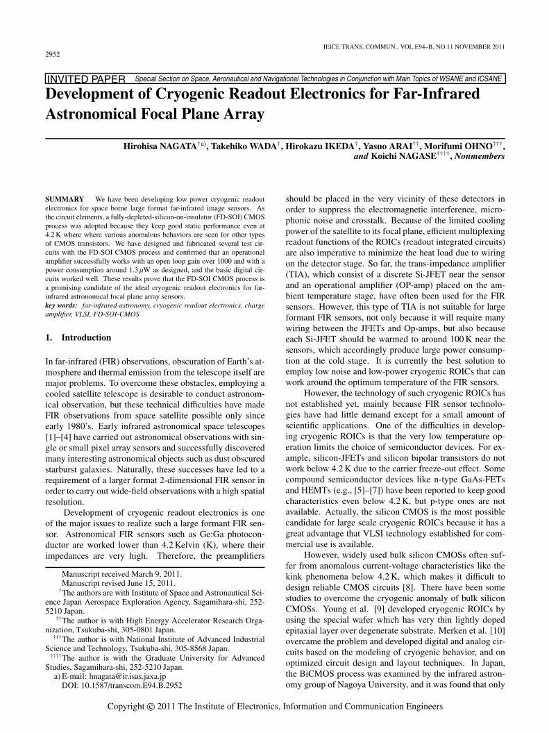
Simple LSI circuits and basic elements were manufacturedin 0.2 μm FD-SOI-CMOS process by OKI semiconductorin 2008 and 2009. Besides the normal type design of theFD-SOI-CMOS, there are source-tied and body-tied designsin the CMOS process. While the body of the normal typeFD-SOI-CMOS is not directly connected with the drain orsource terminals, that of source-tied one is electrically con-nected to the source terminal, and the body-tied one has abody terminal to control the body potential. Though both thesource-tied and body-tied FD-SOI-CMOSs showed goodperformance at 4.2 K in the previous measurement [20], allthe circuits consist of source-tied FD-SOI-CMOSs becauseof their simplicity in designing. Table 1 displays a sum-mary of the manufactured circuits. Basic analog circuits likeoperational amplifier and capacitive transimpedance ampli-fiers (CTIAs) have been fabricated in 2008. On the otherhand, in 2009, we have complementarily fabricated funda-mental digital circuits (such as NAND or Flip-Flops) and 8bit-successive approximation register (SAR) type A-D con-verter consisting of various digital and analog circuits. Fig-ure 1 shows a chip photograph of the experimental produc-tion in 2008, whose chip size is 2.5× 2.5 mm2. We notethat any FET model for applications below 4.2 K has not
Table 1 Summary of the experimental productions.
Analog (2008) Digital (2009)
Operational amplifiers Basic logic components(e.g., NAND, INV, FF)
Single ended amplifiers 8 bit SAR ADCDC-coupled CTIA (DA converter, Registers)AC-coupled CTIA S&H, Multiplexer, and CTIA
Basic circuit elements Basic circuit elements (FETs)(R, C, FETs) Other test circuits
Fig. 1 Photograph of the manufactured cryogenic circuits “Analog” in2008 [20]. The chip size is 2.5 × 2.5 mm2. External large pads are con-nected to the test analog circuits and the basic circuits elements are fabri-cated around inner small pads.
been established yet unlike development of custom LSIs atan ambient temperature. It is currently difficult to design so-phisticated cryogenic circuits only with a circuit simulator.Therefore, we fabricated basic circuits components as thebuilding blocks of the cryogenic ROICs at first in order toverify the dynamic characteristics at 4.2 K.
3. Performance of Single FD-SOI-CMOSs at Cryo-genic Temperatures
3.1 Static Performance
We evaluated source-tied FD-SOI-CMOSs in 0.2 μm pro-cess. The measured FETs are fabricated on the “Analog”chip in 2008. In order to measure the performance at 4.2 K,each “Analog” chip was mounted into a 48-pin ceramic dippackage and wire bonded. The package was mechanically-fixed on a copper sample holder which was mounted on thecopper cold stage of 8-inch liquid helium cryostat, and thenwas cooled down to a liquid nitrogen temperature (77 K)or a liquid helium temperature (4.2 K). We measured staticcharacteristics of the FD-SOI-CMOSs at a room tempera-ture (RT = 293 K), 77 K, and 4.2 K by using Agilent HP4156C Semiconductor Parameter Analyzer. Most of thecryogenic circuits on “Analog” chip are designed using thesource-tied FD-SOI-CMOSs with a gate length of 5 μm,which showed a good performance in the several test sam-
2954IEICE TRANS. COMMUN., VOL.E94–B, NO.11 NOVEMBER 2011
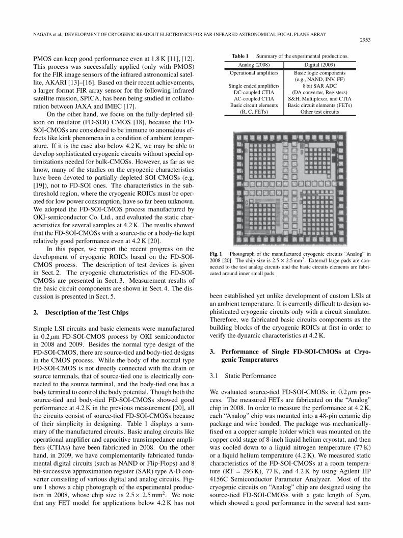
Fig. 2 I-V characteristics of FD-SOI-CMOS (source tied type) at 4.2 Kfor W(μm)/L(μm) = 0.63/5.0. (a) NMOSFET and (b) PMOSFET. VGS(from 1.05 to 1.23 V with 0.023 V) was given for the NMOS and VGS(−1.15 to −1.55 V in step of −0.04 V) was given for the PMOS. Forwardand reverse sweep data of VDS were continuously measured to find hys-teresis effects on the I-V curves.
ples [20]. Here, we report on the measurement results forones with that gate length. Panels (a) and (b) in Fig. 2 showexamples of current-voltage (I-V) characteristics in the sub-threshold region for the source-tied FD-SOI-CMOSs whosegate sizes are W(μm)/L(μm) = 0.63/5.0. Even at 4.2 K,no remarkable anomaly are observed on the I-V curves for∣∣∣(drain − source voltage (VDS)
∣∣∣ ≤ 1 V except for the fol-lowing weak one. The drain resistance becomes slightlylarger near |VDS| = 0 especially for the PMOSs. Thisphenomena is due to the carrier freeze-out effect in lightlydoped region near the drain [22]. On the other hand, thedrain breakdown occurred at VDS = 1.4∼1.5 V for someof the measured NMOSs (Fig. 3) at 77 K and 4.2 K, butthe PMOSs did not suffer from the phenomenon for below|VDS| of 1.5 V in the temperature range because of the largereffective mass of the holes.
Figure 4 shows typical IDS-VGS (gate-source volt-age) characteristics. When the temperature decreases fromRT to 4.2 K, |VGSs| at |IDS| = 0.1 μA increase by 90 mVand 290 mV for the NMOS and the PMOS. Table 2 showssmall signal characteristics of the FD-SOI-CMOSs. Thetransconductance, gm, increase as the operating temperature
Fig. 3 I-V characteristics of the NMOS (a) and the PMOS (b) at 4.2 Kfor the same gate size as in Fig. 2, but |VDS| was swept between 0 and1.5 V in the same way as in Fig. 2. The drain breakdown phenomena areseen around VDS = 1.4 V for the NMOS.
decrease. The gm of SOI-NMOS is similar to twice of that ofPMOS for these temperatures. The drain to source currentin a condition where |VGS| is much less than the thresholdvoltage (off-state IDS) is an another important parameter es-pecially for charge integration amplifiers. The off-state IDSsin Fig. 4, which are limited by the measurement system, areupper limits. Further measurements (for example, by usingon-chip integrators) are needed to obtain this parameter.
3.2 Noise Performance
We measured the noise spectrum in the low frequency regionat 4.2 K for the source tied FD-SOI-CMOSs with a gate sizeof W(μm)/L(μm) = 0.63/5.0. Figure 5 shows the measure-ment circuit. All measurements were carried out under thecondition where drain breakdown phenomena did not occur.The applied voltages are 1.0 V, and 0.1 V for |VD| and |VS|in Fig. 5. The output voltage of the source follower was setto be ∼ 0 V (|IDS| of the measured FET was then biased tobe 0.1 μA) by tuning |VG|, around whose condition analogcircuits in the cryogenic ROICs will be operated. The out-put voltage was acquired by an FFT analyzer (ONOSOKKICF-7200). In order to obtain the input referred noise volt-ages, the acquired output voltages were divided by the total

NAGATA et al.: DEVELOPMENT OF CRYOGENIC READOUT ELECTRONICS FOR FAR-INFRARED ASTRONOMICAL FOCAL PLANE ARRAY2955
Fig. 4 Typical IDS-VGS (gate-source voltage) characteristics of the FD-SOI-CMOS at temperatures of RT, 77 K, and 4.2 K. The upper and lowerpanels show the plots for NMOS and PMOS, respectively.
Table 2 Small signal parameters on the FD-SOI-CMOSs withW(μm)/L(μm) = 0.63/5.0 in the saturation region (|VDS| ∼ 1 V and|IDS| ∼ 0.1 μA).
Temperature NMOS PMOS(K) gm (μS) rd (Ω) gm (μS) rd (Ω)
RT 1.3 > 100 MΩ 1.1 > 100 MΩ77 2.0 > 100 MΩ 1.6 > 100 MΩ4.2 3.0 > 100 MΩ 1.8 > 100 MΩ
gain measured prior to the noise measurements. The totalgain is the product of the source follower gain (0.72 for theNMOS source follower and 0.63 for the PMOS one) and thegain of 110 for the subsequent amplifiers on the RT stage.Figure 6 shows the noise spectrum for one of the source tiedFD-SOI-CMOSs. The noise spectrum densities at 1 Hz andat |IDS| = 0.1 μA are 7–10 μV/
√Hz for both the PMOS and
the NMOS. The discrete fluctuation on the output voltagewas sometimes observed in time domain. It means the RTS(Random Telegraph Signals) noise sometimes occurred inthe low frequency region as a dominant noise component.We did not measure the performance above 1 kHz due tothe limitation of the frequency response on the measurementsystem. Instead, we estimated the input referred channelthermal noise, 8 kT/3 gm, from the static characteristics ofthe FETs. In reference to Table 2, the noise floors are calcu-
Fig. 5 Noise measurement circuit. The measured source follower am-plifier consists of FD-SOI-CMOS and source follower resistor of 1 MΩ,which were placed on the 4.2 K stage. The output of the source followerwas amplified by a low noise silicon JFET source follower buffer and thenby an instrumentation amplifier. The measured total gain by the followingtwo amplifiers on the RT stage, was, 110. The output signal was observedwith an FFT analyzer.
Fig. 6 Input referred noise spectra of the source-tied FD-SOI-CMOSsat 4.2 K. The gate size is W(μm)/L(μm) = 0.63/5.0. These noise spectrawere measured in the configuration of Fig. 5. The bias current was |0.1| μAfor the drain-source voltage of |1 V|. In these measurements, the outputvoltages of the source follower amplifier were set to be approximately 0 Vby turning |VGS|. For the NMOS and the PMOS, the supplied VGs were1.18 V and −1.23 V and the source follower gains (measured at 10 Hz) were0.72 and 0.63. The sharp peaks are due to the electrical interference in thelaboratory environment.
lated to be 7 nV/√
Hz for the NMOS and 9 nV/√
Hz for thePMOS, respectively. Next, we show the result of the sameconfiguration except that the bias current is 1 μA. The RTSnoises on the low frequency spectra was not remarkable forthe PMOSs and the noise levels decreased by approximatelya factor of two. On the other hand, the noise levels did notshow a clear dependence on the bias current for the NMOSs,because the low frequency noises were sometimes remark-able at IDSs of 0.5 μA or 1.0 μA due to the large RTS noises.We have not fully understood the RTS noise performance inthis process yet. Therefore, further studies on the reductionmethod as well as on the noise performance are needed inorder to realize an FIR preamplifier achieving a backgroundlimited performance.
2956IEICE TRANS. COMMUN., VOL.E94–B, NO.11 NOVEMBER 2011
4. Measurement Results on Fundamental Circuits
4.1 Operational Amplifier
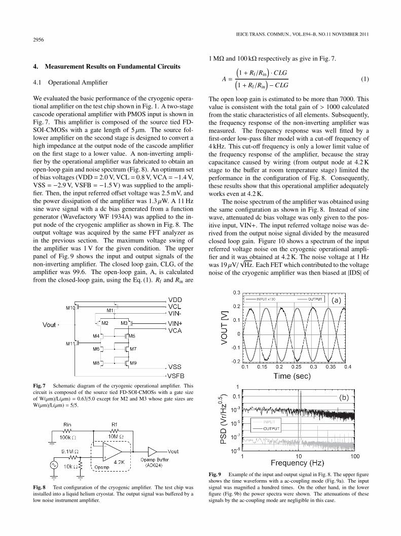
We evaluated the basic performance of the cryogenic opera-tional amplifier on the test chip shown in Fig. 1. A two-stagecascode operational amplifier with PMOS input is shown inFig. 7. This amplifier is composed of the source tied FD-SOI-CMOSs with a gate length of 5 μm. The source fol-lower amplifier on the second stage is designed to convert ahigh impedance at the output node of the cascode amplifieron the first stage to a lower value. A non-inverting ampli-fier by the operational amplifier was fabricated to obtain anopen-loop gain and noise spectrum (Fig. 8). An optimum setof bias voltages (VDD = 2.0 V, VCL = 0.8 V, VCA = −1.4 V,VSS = −2.9 V, VSFB = −1.5 V) was supplied to the ampli-fier. Then, the input referred offset voltage was 2.5 mV, andthe power dissipation of the amplifier was 1.3μW. A 11 Hzsine wave signal with a dc bias generated from a functiongenerator (Wavefactory WF 1934A) was applied to the in-put node of the cryogenic amplifier as shown in Fig. 8. Theoutput voltage was acquired by the same FFT analyzer asin the previous section. The maximum voltage swing ofthe amplifier was 1 V for the given condition. The upperpanel of Fig. 9 shows the input and output signals of thenon-inverting amplifier. The closed loop gain, CLG, of theamplifier was 99.6. The open-loop gain, A, is calculatedfrom the closed-loop gain, using the Eq. (1). Rf and Rin are
Fig. 7 Schematic diagram of the cryogenic operational amplifier. Thiscircuit is composed of the source tied FD-SOI-CMOSs with a gate sizeof W(μm)/L(μm) = 0.63/5.0 except for M2 and M3 whose gate sizes areW(μm)/L(μm) = 5/5.
Fig. 8 Test configuration of the cryogenic amplifier. The test chip wasinstalled into a liquid helium cryostat. The output signal was buffered by alow noise instrument amplifier.
1 MΩ and 100 kΩ respectively as give in Fig. 7.
A =
(1 + Rf/Rin
)·CLG(
1 + Rf/Rin
)− CLG
(1)
The open loop gain is estimated to be more than 7000. Thisvalue is consistent with the total gain of > 1000 calculatedfrom the static characteristics of all elements. Subsequently,the frequency response of the non-inverting amplifier wasmeasured. The frequency response was well fitted by afirst-order low-pass filter model with a cut-off frequency of4 kHz. This cut-off frequency is only a lower limit value ofthe frequency response of the amplifier, because the straycapacitance caused by wiring (from output node at 4.2 Kstage to the buffer at room temperature stage) limited theperformance in the configuration of Fig. 8. Consequently,these results show that this operational amplifier adequatelyworks even at 4.2 K.
The noise spectrum of the amplifier was obtained usingthe same configuration as shown in Fig. 8. Instead of sinewave, attenuated dc bias voltage was only given to the pos-itive input, VIN+. The input referred voltage noise was de-rived from the output noise signal divided by the measuredclosed loop gain. Figure 10 shows a spectrum of the inputreferred voltage noise on the cryogenic operational ampli-fier and it was obtained at 4.2 K. The noise voltage at 1 Hzwas 19 μV/
√Hz. Each FET which contributed to the voltage
noise of the cryogenic amplifier was then biased at |IDS| of
Fig. 9 Example of the input and output signal in Fig. 8. The upper figureshows the time waveforms with a ac-coupling mode (Fig. 9a). The inputsignal was magnified a hundred times. On the other hand, in the lowerfigure (Fig. 9b) the power spectra were shown. The attenuations of thesesignals by the ac-coupling mode are negligible in this case.
NAGATA et al.: DEVELOPMENT OF CRYOGENIC READOUT ELECTRONICS FOR FAR-INFRARED ASTRONOMICAL FOCAL PLANE ARRAY2957
Fig. 10 Input referred noise of the cryogenic operational amplifier at4.2 K.
Table 3 Summary of the performance measurement on the cryogenicamplifier.
Parameters result
Operating temperature 4.2 Kopen loop gain 7000Voltage swing 1 V
Input referred noise voltage at 1 Hz 19 μV/√
HzPower consumption 1.3 μW
Input referred offset voltage 2.5 mVGain-bandwidth product > 0.4 MHz
0.1 μA. Assuming that the input referred noise of each FETcomposing the cryogenic operational amplifier is inverselyproportional to the square root of the gate area at 4.2 K, theinput referred noise of the amplifier, vn,opamp, is given as fol-lows [23],
vn,opamp ≈√
2v2n, W/L=0.63/5 +2v2n, W/L=0.63/5
(5/0.63), (2)
where vn, W/L=0.63/5 is the noise of a single FET whose gatesize of W(μm)/L(μm) = 0.63/5.0. Considering that theinput referred noise of a single FET is 7–10 μV/
√Hz at
1 Hz for the |IDS| of 0.1 μA, vn,opamp is estimated to be 11–15 μV/
√Hz at 1 Hz. The measured noise is slightly higher
than the expected one. If the assumption is correct, the inputreferred noises of the FETs composing the amplifier may behigher than those of single FETs described in Sect. 3.2. Fur-ther studies on the variation and on the gate area dependencyof the noise performance are needed to compare the ampli-fier design with measurement results. Here, we note that thetotal thermal noise generated by resistors, Rin, Rf in Fig. 8is 40 nV/
√Hz as an input referred value. The noise com-
ponents are, therefore, negligible in these measurements.The performance of the cryogenic operational amplifier de-scribed in this section is summarized on Table 3.
4.2 Basic Digital Circuits
We measured the basic digital circuits fabricated on the
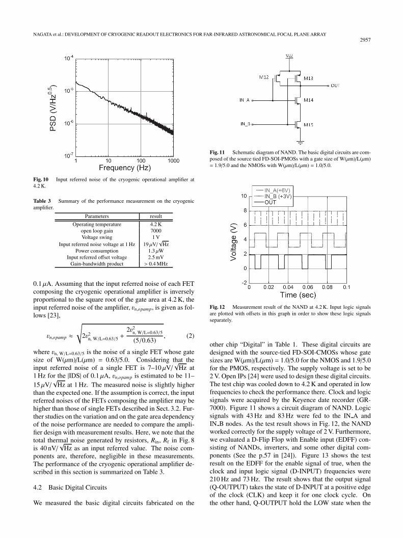
Fig. 11 Schematic diagram of NAND. The basic digital circuits are com-posed of the source tied FD-SOI-PMOSs with a gate size of W(μm)/L(μm)= 1.9/5.0 and the NMOSs with W(μm)/L(μm) = 1.0/5.0.
Fig. 12 Measurement result of the NAND at 4.2 K. Input logic signalsare plotted with offsets in this graph in order to show these logic signalsseparately.
other chip “Digital” in Table 1. These digital circuits aredesigned with the source-tied FD-SOI-CMOSs whose gatesizes are W(μm)/L(μm) = 1.0/5.0 for the NMOS and 1.9/5.0for the PMOS, respectively. The supply voltage is set to be2 V. Open IPs [24] were used to design these digital circuits.The test chip was cooled down to 4.2 K and operated in lowfrequencies to check the performance there. Clock and logicsignals were acquired by the Keyence date recorder (GR-7000). Figure 11 shows a circuit diagram of NAND. Logicsignals with 43 Hz and 83 Hz were fed to the IN A andIN B nodes. As the test result shows in Fig. 12, the NANDworked correctly for the supply voltage of 2 V. Furthermore,we evaluated a D-Flip Flop with Enable input (EDFF) con-sisting of NANDs, inverters, and some other digital com-ponents (See the p.57 in [24]). Figure 13 shows the testresult on the EDFF for the enable signal of true, when theclock and input logic signal (D-INPUT) frequencies were210 Hz and 73 Hz. The result shows that the output signal(Q-OUTPUT) takes the state of D-INPUT at a positive edgeof the clock (CLK) and keep it for one clock cycle. Onthe other hand, Q-OUTPUT hold the LOW state when the

2958IEICE TRANS. COMMUN., VOL.E94–B, NO.11 NOVEMBER 2011
Fig. 13 Measurement result of a D-Flip Flop with Enable input (EDFF)at 4.2 K. Input logic signal (D-INPUT) and clock (CLK) are plotted withoffsets in this graph. Q-OUTPUT means the output signal.
enable signal was false. The EDFF worked reasonably at4.2 K. Consequently, the designed basic digital circuits canwork at 4.2 K as designed at least in low frequency region.
We also measured the delay times, τLH and τHL, fromthe rising and falling edges of the measurements in Fig. 13.τLH (τHL) is defined as the time between the midpoint ofthe falling (rising) edge of the clock and that of the rising(falling) edge of the following Q-OUTPUT. In this measure-ment, τLH and τHL are 17 μs and 23 μs, respectively. Thereason why τLH is shorter than τHL is possibly because theNMOS in the EDFF had a higher driving capability than thePMOS. Therefore, the higher frequency limit of the EDFF,1/ (τLH + τHL), is 25 kHz. This result is a lower limit value,because the frequency responses of these digital circuitswere limited by the output load capacitance caused by thewiring as described in Sect. 4.1.
5. Discussion
We measured the cryogenic performance of the FD-SOI-CMOSs in the sub-threshold region. They keep good staticcharacteristics between RT and 4.2 K. According to [20],the static and noise performances of the FD-SOI-CMOSproduced by OKI semiconductor did not change between4.2 K and 2 K. Therefore we expect that the ROIC basedon the process can work at 2 K where infrared sensorsshould be operated. In reference to [20], we can expectthat the read noise of a proper designed preamplifier em-ploying the FD-SOI-CMOSs will achieve a background lim-ited performance when a Ge:Ga photoconductor is oper-ated under a typical background condition. Therefore, theFD-SOI-CMOS is an emerging candidate as a basic com-ponent of cryogenic preamplifier for FIR image sensors.Combination with Ge Blocked Impurity Band (BIB) detec-tors that is recently emerging with surface-activated waferbonding (SAB) technology and molecular beam epitaxy(MBE) technology are urgent targets [25]–[27]. The FD-
SOI-CMOS has another merit that the temperature variationon the threshold voltage is relatively small, compared withbulk CMOSs [22]. For example, the variations on |VGS|at |IDS| of 0.1 μA for the FD-SOI-CMOS were 90 mV forthe NMOS and 290 mV for the PMOS, while that of a bulkPMOS was ∼ 600 mV [28]. This characteristic will helpus to develop VLSIs that can be operated over a very widetemperature range (from 300 K to 4.2 K) without tuning biasvoltages. Furthermore, FD-SOI-CMOS devices have resis-tance characteristics against high energy particle radiation.Hirose et al. [29], [30] have shown that 128-Kbit SRAMsusing a rad-hard circuit design in a 0.2 μm FD-SOI-CMOSprocess have high tolerance for Single Event Latch up, Sin-gle Event Upset, and Total Ionizing Dose. Low power VLSIwith high tolerance for temperature variation and high en-ergy particle radiation should be useful for various scientificfield including space explorations or astronomy.
Based on the above mentioned CMOS characteristics,we first developed cryogenic operational amplifier in theFD-SOI-CMOS process, which means that various analogcircuits can be developed with this process. The cryogenicoperational amplifier itself, of course, can be used for versa-tile applications like preamplifiers, switched capacitors forS&H circuits, and Wilkinson ADCs. The basic digital cir-cuits as complicated as EDFF also operated correctly at leastin the low frequency region for the supply voltage of 2 V.These results will lead us to sophisticated circuits consistingof analog and digital components without special optimiza-tions.
Some unevaluated parameters still remain. The gateleakage and the off-state drain-source currents of the FD-SOI-CMOS are critical parameters to operate very highimpedance detectors like BIB type ones. Moreover, mea-surement on the noise performance under a high impedanceconfiguration should be needed because some kind of noiselike dielectric polarization noise appears in such a configu-ration [31]. Thus, these parameters should be obtained to es-timate the practical performance of the cryogenic integratedcircuits.
Acknowledgment
This work was carried out with kind cooperation of Ad-vanced Technology Center, National Astronomical Obser-vatory of Japan. This work was supported by KAKENHI(21760321, 23340053, 20244016). This study was also sup-ported by the FY2007 and FY2009 Japan Aerospace Explo-ration Agency president fund.
References
[1] G. Neugebauer, H.J. Habing, R. van Duinen, H.H. Aumann,B. Baud, C.A. Beichman, D.A. Beintema, N. Boggess, P.E.Clegg, T. de Jong, J.P. Emerson, T.N. Gautier, F.C. Gillett, S.Harris, M.G. Hauser, J.R. Houck, R.E. Jennings, F.J. Low, P.L.Marsden, G. Miley, F.M. Olnon, S.R. Pottasch, E. Raimond, M.Rowan-Robinson, B.T. Soifer, R.G. Walker, P.R. Wesselius, and E.Young, “The Infrared Astronomical Satellite (IRAS) mission,” APJ,
NAGATA et al.: DEVELOPMENT OF CRYOGENIC READOUT ELECTRONICS FOR FAR-INFRARED ASTRONOMICAL FOCAL PLANE ARRAY2959
278, pp.L1–L6, 1984.[2] The COBE mission, “The COBE mission — Its design and perfor-
mance two years after launch,” APJ, 397, pp.420–429, 1992.[3] M.F. Kessler, J.A. Steinz, M.E. Anderegg, J. Clavel, G. Drechsel,
P. Estaria, J. Faelker, J.R. Riedinger, A. Robson, B.G. Taylor, andS. Ximenez de Ferran, “The Infrared Space Observatory (ISO) mis-sion,” A&A, 315, pp.L27–L31, 1996.
[4] H. Murakami, M.M. Freund, K. Ganga, H. Guo, T. Hirao, N.Hiromoto, M. Kawada, A.E. Lange, S. Makiuti, H. Matsuhara, T.Matsumoto, S. Matsuura, M. Murakami, T. Nakagawa, M. Narita,M. Noda, H. Okuda, K. Okumura, T. Onaka, T.L. Roellig, S. Sato, H.Shibai, B.J. Smith, T. Tanabe, M. Tanaka, T. Watabe, I. Yamamura,and L. Yuen, “The IRTS (Infrared Telescope in Space) mission,”PASJ, 48, pp.L41–L46, 1996.
[5] A. Alessandrello, C. Brofferio, D.V. Camin, A. Giuliani, G. Pessina,and E. Previtali, “Cryogenic voltage-sensitive preamplifier usingGaAs MESFETs of low 1/f noise,” NIMA, vol.295, pp.405–410,1990.
[6] M. Fujiwara, M. Sasaki, and M. Akiba, “Reduction method for low-frequency noise of GaAs junction field-effect transistor at a cryo-genic temperature,” Appl. Phys. Lett., vol.80, pp.1844–1846, 2002.
[7] S.J.C. Yates, A. Benoit, Y. Jin, Ph. Camus, A. Cavanna, T. Durand,B. Etienne, U. Gennser, E. Gremion, C. Hoffmann, S. Leclercq, andCh. Ulysse, “The use of HEMTs in multiplexing large arrays of highimpedance LTDs,” NIMA, vol.559, pp.829–831, 2006.
[8] R.M. Glidden, S.C. Lizotte, J.S. Cable, L.W. Mason, and C. Cao,“Optimization of cryogenic CMOS processes for sub-10 K applica-tions,” Proc. SPIE, vol.1684, pp.2–39, 1992.
[9] E.T. Young, J.T. Davis, C.L. Thompson, G.H. Rieke, G. Rivlis, R.Schnurr, J. Cadien, L. Davidson, G.S. Winters, and K.A. Kormos,“Far-infrared imaging array for SIRTF,” Proc. SPIE, vol.3354,pp.57–65, 1998.
[10] P. Merken, T. Souverijns, J. Putzeys, Y. Creten, and C.V. Hoof, “Lownoise, low power readout electronics circuit development in stan-dard CMOS technology for 4K applications,” Proc. SPIE, vol.6275,627516, 2006.
[11] M. Noda, H. Shibai, T. Watabe, T. Hirao, H. Yoda, H. Nagata, T.Nakagawa, and M. Kawada, “Evaluation of charge-integrating am-plifier with silicon MOSFETs for cryogenic readout,” Proc. SPIE,vol.3354, pp.247–252, 1998.
[12] T. Hirao, Y. Hibi, M. Kawada, H. Nagata, H. Shibai, T. Watabe,M. Noda, and T. Nakagawa, “Cryogenic readout electronics withsilicon P-MOSFETs for the infrared astronomical satellite, ASTRO-F,” Advances in Space Research, vol.30, pp.2117–2122, 2002.
[13] H. Nagata, H. Shibai, T. Hirao, T. Watabe, M. Noda, Y. Hibi, M.Kawada, and T. Nakagawa, “Cryogenic capacitive transimpedanceamplifier for astronomical infrared detectors,” IEEE Trans. Electron,vol.51, no.2, pp.270–278, 2004.
[14] M. Shuji, I. Yosuke, S. Mai, K. Hidehiro, N. Takao, P. Michael,F. Mikio, H. Takanori, K. Mitsunobu, S. Hiroshi, and W. Toyoki,“Monolithic Ge:Ga two-dimensional array for FIS instrument onASTRO-F,” Proc. SPIE, vol.4850, p.902, 2002.
[15] Y. Doi, S. Hirooka, A. Sato, M. Kawada, H. Shibai, Y. Okamura,S. Makiuti, T. Nakagawa, N. Hiromoto, and M. Fujiwara, “Large-format and compact stressed Ge:Ga array for the ASTRO-F (IRIS)mission,” Advances in Space Research, vol.30, pp.2099–2104,2002.
[16] M. Fujiwara, T. Hirao, M. Kawada, H. Shibai, S. Matsuura,H. Kaneda, M. Patrashin, and T. Nakagawa, “Development of agallium-doped germanium far-infrared photoconductor direct hybridtwo-dimensional array,” Appl. Opt., vol.42, pp.2166–2173, 2003.
[17] M. Shirahata, S. Matsuura, T. Nakagawa, T. Wada, S. Kamiya, M.Kawada, Y. Sawayama, Y. Doi, H. Kawada, Y. Creten, B. Okcan,W. Raab, and A. Poglitsch, “Development of a far-infrared Ge:Gamonolithic array for a possible application to SPICA,” Proc. SPIE,vol.7741, 77410B, 2010.
[18] A. Uchiyama, S. Baba, Y. Nagatomo, and J. Ida, “Fully depleted
SOI technology for ultra low power digital and RF applications,”2006 IEEE International SOI Conference, pp.15–16, 2006.
[19] E. Simoen and C. Claeys, “The cryogenic operation of partially de-pleted silicon-on-insulator inverters,” IEEE Trans. Electron., vol.42,no.6, pp.1100–1105, 1995.
[20] H. Nagata, T. Wada, H. Ikeda, Y. Arai, and M. Ohno, “Develop-ment of cryogenic readout electronics using fully-depleted-silicon-on-insulator CMOS process for future space borne far-infrared im-age sensors,” AIP Conference Proceedings, vol.1185, pp.267–270,2009.
[21] V.S. Lysenko, I.P. Tyagulski, Y.V. Gomeniuk, and I.N. Osiyuk, “Ef-fect of oxide–semiconductor interface traps on low-temperature op-eration of MOSFETs,” Microelectronics Reliability, vol.40, pp.735–738, 2000.
[22] F. Balestra and G. Ghibaudo, ed., Device and Circuit Cryogenic Op-eration for Low Temperature Electronics, Kluwer Academic Pub-lishers, 2001.
[23] B. Razavi, “Operational amplifiers,” in Design of Analog CMOSIntegrated Circuits, McGraw Hill Higher Education, 2003.
[24] H. Ikeda, “Analog-VLSI Open-IP Project,” http://research.kek.jp/people/ikeda/openIP/, 2005.
[25] T. Wada, H. Kaneda, R. Kano, K. Wada, T. Suzuki, K. Watanabe,and Y. Kiriyama, “Development of Germanium BIB detector withsurface activated bonding and Molecular-Beam Epitaxial crystalgrowth,” International Conference on Infrared Millimeter and Ter-ahertz Waves, 2010 IEEE, 2010.
[26] K. Watanabe, K. Wada, H. Kaneda, K. Ide, M. Kato, and T. Wada,“Microscopic and electrical properties of Ge/Ge interfaces bondedby surface-activated wafer bonding technology,” Jpn. J. Appl. Phys.,vol.50, no.1, pp.015701-1–015701-5, 2011.
[27] H. Kaneda, T. Wada, S. Oyabu, R. Kano, Y. Kiriyama, Y. Hattori,T. Suzuki, K. Ide, M. Kato, and K. Watanabe, “Electrical and Pho-toconductive Properties at 2 K of Germanium p+ –i Junction De-vice Fabricated by Surface-Activated Wafer Bonding,” Jpn. J. Appl.Phys., vol.50, no.6, 066503, 2011.
[28] H. Nagata, Master Thesis, Nagoya University, 1999.[29] K. Hirose, H. Saito, M. Akiyama, M. Arakaki, Y. Kuroda, S. Ishii,
and K. Nakano, “Total-dose and single-event-upset (SEU) resistancein advanced SRAMs fabricated on SOI using 0.2 μm design rules,”2001 IEEE Radiation Effects Data Workshop, pp.48–50, 2001.
[30] K. Hirose, H. Saito, Y. Kuroda, S. Ishii, Y. Fukuoka, and D.Takahashi, “SEU resistance in advanced SOI-SRAMs fabricatedby commercial technology using a rad-hard circuit design,” IEEETrans. Nucl. Sci., vol.49, no.6, pp.2965–2968, 2002.
[31] M. Akiba and M. Fujiwara, “Ultralow-noise near-infrared detectionsystem with a Si p-i-n photodiode,” Opt. Lett., vol.28, pp.1010–1012, 2003.
Hirohisa Nagata received the B.S. degreein earth and planetary sciences from Kobe Uni-versity, Kobe, Japan in 1997. He received theM.S. and Ph.D. degrees in particle and astro-physical sciences from Nagoya University, Na-goya, Japan, in 1999 and 2003, respectively.From 2003 to 2007, he was a Research fel-low at the National Astronomical Observatoryof Japan, Tokyo. From 2007 to 2010, he was anAerospace Project Research Associate of JapanAerospace Exploration Agency (JAXA). Since
2010, he has been a Collaborative Research Fellow at JAXA. His currentresearch interests include cryogenic readout electronics for various scien-tific applications.

2960IEICE TRANS. COMMUN., VOL.E94–B, NO.11 NOVEMBER 2011
Takehiko Wada received the B.S., M.S.and D.S. degreesfrom the University of Tokyo,Tokyo, Japan in 1992, 1994 and 1997, respec-tively. He is currently an Assistant Professorof Institute of Space and Astronautical Science(ISAS) in Japan Aerospace Exploration Agency(JAXA). He has worked on the development andoperation of the first Japanese infrared astro-nomical satellite, AKARI, for ten years. His re-search interest includes infrared astronomy, thebirth and evolution of galaxies, and the develop-
ment of instrumentations for infrared astronomy.
Hirokazu Ikeda was born in Tsukuba,Japan, in 1950. He received the B.S. degreein physics from Kyoto university in 1973, and,then, M.S. and Ph.D. degrees in physics fromthe University of Tokyo, in 1975, and 1978, re-spectively. He joined the High Energy Acceler-ator Research Organization (KEK) in 1978. Hemoved to the Institute of Space and Astronau-tical Science, Japan (ISAS), in 2005, which isa part of Japan Aerospace Exploration Agency(JAXA). His current research interests include
VLSI analog circuit and radiation sensors for space craft missions as wellas high energy physics and astrophysics. He is a member of the PhysicalSociety of Japan, and IEEE Nuclear & Plasma Science Society as well asSolid State Circuit Society.
Yasuo Arai received Ph.D. degrees in nu-clear science from Tohoku University, Sendai,Japan, in 1982. Currently, he is working atthe High Energy Accelerator Research Organi-zation, KEK, and his present position is profes-sor in the Institute of Particle and Nuclear Stud-ies, and belong to Electronics System group.His research interests are developments of ra-diation detector readout electronics. Especially,He have developed several TDC LSIs for high-energy experiments such as the ATLAS and
the PHENIX experiments and Lunar exploration satellite KAGUYA. Hispresent interest is a development of monolithic pixel detectors for radiationimaging using a SOI (Silicon-On-Insulator) technology.
Morifumi Ohno received the M.S. de-gree in electrical engineering from the TokyoUniversity of Agriculture and Technology, in1983 and the Ph.D. degree in electronic mate-rials science from the Graduate School of Elec-tronic Science and Technology, Shizuoka Uni-versity, in 1986. He had join Oki Electric In-dustry Co., Ltd. (present, OKI SemiconductorCo., Ltd.), where he engaged in the R&D of ad-vanced NVRAM(FeRAM) and FD-SOI devices.In 2009, He joined as an invited researcher in the
National Institute of Advanced Industrial Science and Technology (AIST)in Tsukuba, Japan., where he has been currently involved in the design,simulation, and characterization of nano-electronic devices.
Koichi Nagase received the B.S. de-gree from Tokyo University of Science, Tokyo,Japan in 2010. Currently, he works for the D.S.degree at the Department of Space and Astro-nautical Science in School of Physical Sciences,The Graduate University for Advanced Studies[SOKENDAI], Kanagawa, Japan. His researchinterest includes infrared astronomy.