development of a serial powering scheme and a versatile
TRANSCRIPT

Universität Bonn Physikalisches Institut
Development of a serial powering scheme and
a versatile characterization system for the
ATLAS pixel detector upgrade
Viacheslav Filimonov
In order to increase the probability of new discoveries the LHC will be upgraded to the HL-LHC. The
upgrade of the ATLAS detector is an essential part of this program. The entire ATLAS tracking system
will be replaced by an all-silicon detector called Inner Tracker (ITk) which should be able to withstand
the increased luminosity of 5×1034
cm-2
s-1
. The work presented in this thesis is focused on the ATLAS
ITk pixel detector upgrade. Advanced silicon pixel detectors will be an essential part of the ITk pixel
detector where they will be used for tracking and vertexing. Characterization of the pixel detectors is one
of the required tasks for a successful ATLAS tracker upgrade. Therefore, the work presented in this thesis
includes the development of a versatile and modular test system for advanced silicon pixel detectors for
the HL-LHC. The performance of the system is verified. Single and quad FE-I4 modules functionalities
are characterized with the developed system. The reduction of the material budget of the ATLAS ITk
pixel detector is essential for a successful operation at high luminosity. Therefore, a low mass, efficient
power distribution scheme to power detector modules (serial powering scheme) is investigated as well in
the framework of this thesis. A serially powered pixel detector prototype is built with all the components
that are needed for current distribution, data transmission, sensor biasing, bypassing and redundancy in
order to prove the feasibility of implementing the serial powering scheme in the ITk. Detailed
investigations of the electrical performance of the detector prototype equipped with FE-I4 quad modules
are made with the help of the developed readout system.
Physikalisches Institut der
Universität Bonn
Nussallee 12
D-53115 Bonn
BONN-IR-2017-06
August 2017
ISSN-0172-8741


Development of a serial powering scheme and
a versatile characterization system for the
ATLAS pixel detector upgrade
Dissertation
zur
Erlangung des Doktorgrades (Dr. rer. nat.)
der
Mathematisch-Naturwissenschaftlichen Fakultät
der
Rheinischen Friedrich-Wilhelms-Universität Bonn
von
Viacheslav Filimonov aus
Moskau, Russland
Bonn, 2017

Dieser Forschungsbericht wurde als Dissertation von der Mathematisch-Naturwissenschaftlichen
Fakultät der Universität Bonn angenommen und ist auf dem Hochschulschriftenserver der ULB
Bonn http://hss.ulb.uni-bonn.de/diss_online elektronisch publiziert.
1. Gutachter: Prof. Dr. Norbert Wermes
2. Gutachter: Prof. Dr. Klaus Desch
Tag der Promotion: 18.07.2017
Erscheinungsjahr: 2017

Contents
1 Introduction .................................................................................................................................. 1
2 The experimental setup: The Large Hadron Collider and the ATLAS experiment ..................... 3
2.1 The Large Hadron Collider ................................................................................................... 3
2.1.1 Accelerator ...................................................................................................................... 3
2.1.2 Experiments at the Large Hadron Collider ..................................................................... 4
2.2 The ATLAS experiment ........................................................................................................ 4
2.2.1 Detector requirements..................................................................................................... 4
2.2.2 Detector layout ............................................................................................................... 5
2.2.3 The ATLAS Pixel Detector ............................................................................................ 6
2.3 The ATLAS Tracker upgrade ............................................................................................... 9
3 Silicon pixel detectors for tracking in HEP ............................................................................... 12
3.1 Transverse momentum resolution ....................................................................................... 12
3.2 Vertex resolution ................................................................................................................. 13
3.3 Radiation length .................................................................................................................. 14
3.4 Multiple scattering............................................................................................................... 15
3.5 Energy deposition of photons .............................................................................................. 15
3.6 Hybrid pixel detectors ......................................................................................................... 17
3.6.1 Pixel sensor ................................................................................................................... 18
3.6.2 Readout chip ................................................................................................................. 21
3.6.3 Pixel module ................................................................................................................. 26
4 Development of a versatile and modular test system for Advanced Silicon Pixel Detectors for
HL-LHC ........................................................................................................................................ 29
4.1 USBpix readout system overview and upgrade motivation ................................................ 29
4.1.1 USBpix readout system overview ................................................................................ 29
4.1.2 Upgrade motivation ...................................................................................................... 31

4.2 USBpix readout system upgrade ......................................................................................... 32
4.3 USBpix3 readout system overview ..................................................................................... 34
4.4 Firmware, hardware and software of the USBpix3 readout system .................................... 35
4.4.1 Firmware of the USBpix3............................................................................................. 36
4.4.2 Carrier boards for the USBpix3 .................................................................................... 37
4.4.3 PyBAR readout framework adaptation to the USBpix3 ............................................... 40
4.5 Performance and functionality tests for the USBpix3 ......................................................... 41
4.5.1 USB 3.0 microcontroller and FPGA firmware tests ..................................................... 41
4.5.2 Hardware design tests ................................................................................................... 43
4.5.3 Configuration and testing prior to distribution ............................................................. 48
4.6 Performance with FE-I4 chips and modules ....................................................................... 48
4.6.1 Characterization of single FE-I4 chip functionalities with the USBpix3 ..................... 49
4.6.2 Characterization of quad FE-I4 module functionalities with the USBpix3 .................. 56
5 Serial powering scheme ............................................................................................................. 62
5.1 Motivation for serial powering in ATLAS .......................................................................... 62
5.2 Serial powering concept ...................................................................................................... 64
5.3 Serial powering requirements.............................................................................................. 66
5.3.1 Current distribution and shunt-LDO regulator ............................................................. 67
5.3.2 Bypass scheme .............................................................................................................. 70
5.3.3 AC-coupled data transmission ...................................................................................... 72
5.3.4 High voltage distribution .............................................................................................. 74
6 A serial powering pixel stave prototype for the ATLAS ITk upgrade ...................................... 75
6.1 Detector prototype characterization setup ........................................................................... 75
6.2 Preparation and characterization of the serially powered FE-I4 quad modules .................. 81
6.3 Characterization of the serially powered detector prototype .............................................. 81
6.3.1 Pixel matrix performance ............................................................................................. 82
6.3.2 Minimum threshold operation and noise occupancy .................................................... 84
6.3.3 Influence of consecutive triggers on threshold and noise occupancy .......................... 88
6.3.4 Performance studies with noisy modules ................................................................... 101

6.3.5 Performance studies with bypassed modules ............................................................. 104
6.3.6 Crosstalk test............................................................................................................... 110
6.3.7 Source scan ................................................................................................................. 111
7 Conclusion and Outlook........................................................................................................... 115
Bibliography ............................................................................................................................... 118
Appendix ..................................................................................................................................... 123
Alternative upgrade options considered for the USBpix ........................................................ 123
Firmware, hardware and software of the USBpix3 readout system ........................................ 124
Firmware of the USBpix3.................................................................................................... 124
Carrier boards for the USBpix3 ........................................................................................... 129
PyBAR readout framework adaptation to the USBpix3 ...................................................... 136


1
Chapter 1
Introduction
Three out of four known forces in the universe as well as the fundamental structure of matter are
described by the Standard Model of particle physics. This theory says that all matter around us is
made of elementary particles (fermions) that are divided into two basic types called quarks and
leptons. In total there are six quarks and six leptons which are arranged in three generations. The
first generation consists of the most stable and lightest particles that form all stable matter in the
universe. The second and third generations consist of less stable and heavier particles that
quickly decay to the more stable particles.
The interaction between fermions is mediated with the help of force-carrier particles that are
called bosons. There is a corresponding boson for each fundamental force. The strong force acts
between color charged particles via the gluon, the electromagnetic force acts between all charged
particles by the exchange of photons, the weak force acts between all fermions via the W and Z
bosons. The Higgs field, the energy field which is thought to exist everywhere in the universe,
gives mass to the particles in the Standard Model as they pass through it via massive scalar
bosons, called the Higgs bosons. All the elements of the Standard Model are shown in Figure
1.1.
Figure 1.1: The Standard Model of particle physics

2
The Standard Model is the best description of the subatomic world, however it can’t explain for
example the hierarchy problem, the nature of the dark matter and the matter/anti matter
asymmetry. These phenomena are tried to be explained by extensions to the Standard Model that
are summarized under the term “Beyond the Standard Model”. Supersymmetry is one of the
extensions, where every particle of the Standard Model has a supersymmetric partner.
Few years ago a new particle consistent with the Higgs boson was observed in the mass region
around 126 GeV at ATLAS and CMS experiments at CERN’s Large Hadron Collider (LHC) [1,
2]. It has been proved that this particle is the Higgs boson predicted by the Standard Model.
Collider experiments with high luminosity and energy such as LHC are needed in order to
produce and observe Higgs bosons and to investigate other new phenomena. Chapter 2 will
explain the details of the LHC and the ATLAS experiment.
It is also necessary to upgrade the LHC and its experiments in order to increase the probability of
new discoveries. The work presented in this thesis is focused on the ATLAS Tracker upgrade
which will be described in Chapter 2. During the LHC Long Shutdown 3 (LS3) starting at the
end of 2023 the entire ATLAS tracking system will be replaced by an all-silicon detector called
Inner Tracker (ITk). Its pixel detector will include five innermost layers, instrumented with new
readout electronics and sensor technologies in order to withstand the harsh radiation and
occupancy environment of the HL-LHC and to improve the tracking performance. Advanced
silicon pixel detectors will be an essential part of the ITk pixel detector. Chapter 3 will describe
these detectors with respect to their application for tracking at the HL-LHC. Characterization of
the pixel detectors is one of the required tasks for a successful ATLAS Tracker upgrade. Chapter
4 will describe a development of a versatile and modular test system for advanced silicon pixel
detectors for HL-LHC.
One of the main challenges for the ATLAS ITk Phase II Pixel upgrade is a low mass, efficient
power distribution to power detector modules. This requires a powering scheme alternative to the
parallel (direct) powering which is currently used. Serial powering scheme was chosen as the
baseline for the ITk pixel system. Chapter 5 will give a motivation for serial powering and
explain the serial powering concept and its requirements. Chapter 6 will describe a serially
powered pixel detector prototype that was built with all the components that are needed for
current distribution, data transmission, sensor biasing, bypassing and redundancy in order to
prove the feasibility of implementing the serial powering scheme in the ITk. Detailed
investigations of the electrical performance of the serially powered stave, equipped with FE-I4
quad modules, including threshold homogeneity, noise occupancy, robustness against noise,
crosstalk and power failures, operation with low detection threshold and consecutive trigger
commands and performance with radioactive source will be shown as well in Chapter 6.
Chapter 7 will summarize the results of this work and propose further developments and tests for
the described systems and concepts.

3
Chapter 2
The experimental setup: The Large Hadron Collider
and the ATLAS experiment
2.1 The Large Hadron Collider
2.1.1 Accelerator
The Large Hadron collider (LHC) [3] is currently the biggest of all existing particle accelerators.
It is located at the European Organization for Nuclear Research (CERN) as you can see in Figure
2.1. The length of its tunnel is 26.7 km.
Figure 2.1: An underground view of the LHC tunnel and four of its main experiments [4]
The LHC is designed as a proton-proton collider with a center of mass energy of 14 TeV and is
suitable for a wide range of observations of new phenomena including the Standard Model Higgs
boson as well as for precise measurements of the Standard Model parameters. Design luminosity
of the LHC is 1034
cm-2
s-1
. Bunches of 1011
protons are accelerated and collide at specific

The experimental setup: The Large Hadron Collider and the ATLAS experiment
4
collision points with 25 ns spacing between them (bunch crossing). About 25 proton-proton
collisions take place per bunch crossing.
2.1.2 Experiments at the Large Hadron Collider
Figure 2.1 shows as well four experiments located at the collision points of the LHC. ATLAS (A
Toroidal LHC ApparatuS) and CMS (Compact Muon Solenoid) are general purpose experiments
aiming to use the design luminosity of the LHC fully in order to examine the Higgs-mechanism
and to explore new physics. LHCb (Large Hadron Collider beauty) is an experiment with
reduced luminosity (1032
cm-2
s-1
) which is optimized for studying b-physics and cp-violation.
ALICE (A Large Ion Collider Experiment) is specialized in heavy ion physics due to the fact that
the LHC can collide not only proton-proton beams but also heavy ions (lead nuclei) with design
luminosity of 1027
cm-2
s-1
.
2.2 The ATLAS experiment
As it was mentioned in the previous section the ATLAS experiment is a general purpose
experiment aiming to use the design luminosity of the LHC fully in order to examine the Higgs-
mechanism and to explore new physics. ATLAS [5, 6] has a diameter of 25 m and a length of 44
m and therefore is the biggest experiment at the LHC. A total weight of ATLAS is 7000 tons.
2.2.1 Detector requirements
A number of requirements have to be fulfilled by the ATLAS detector in order to fully use the
LHC physics potential. The design of the experiment should be made ensuring the detector is
able to withstand particle energies and multiplicities, interaction rates and radiation doses.
Sensors and electronics have to be radiation-hard in order to withstand the harsh radiation and
occupancy environment of the LHC. They should be fast enough too. These are the operational
requirements for the detector.
A number of physics requirements have to be fulfilled as well to be able to perform precision
measurements. In order to minimize the influence of overlapping events the detector needs to
have high granularity. It also has to be composed of several sub-detectors responsible for:

2.2 The ATLAS experiment
5
Sufficient track reconstruction efficiency and charged particle momentum resolution as
well as electron identification.
Photon and electron identification and energy measurement as well as missing transverse
energy and jet measurements that are performed with the help of electromagnetic
calorimetry and hadronic calorimetry respectively.
Muon identification and momentum resolution.
In order to reach an adequate trigger rate for interesting physics processes the detector should
have efficient triggering capability with sufficient background rejection.
2.2.2 Detector layout
All the requirements mentioned above lead to a specific detector structure where each sub-
detector provides certain functions (Figure 2.2).
Figure 2.2: The layout of the ATLAS detector [7]
The biggest sub-detector in ATLAS is the muon tracking system. Its maximum diameter is 25 m.
The muon tracking system is the outermost sub-detector in ATLAS and is used for muon
identification and momentum resolution. Track measurement in this system is performed with

The experimental setup: The Large Hadron Collider and the ATLAS experiment
6
the help of monitored drift tubes. Momentum measurement is performed with the help of toroid
magnet coils that are used to provide a bending power.
The next sub-detectors if moving closer to the interaction point are the calorimeters. They
perform photon and electron identification and energy measurement as well as missing
transverse energy and jet measurements. The electromagnetic calorimeter uses liquid argon as
active material due to the fact that it is exposed to high radiation. Liquid argon is used as well for
the hadronic end-cap and forward calorimeters for the same reason. Scintillating tiles are used
for the barrel part of the hadronic calorimeter.
The sub-detector which is the closest to the interaction point is the inner detector. The innermost
part of the inner detector, the pixel detector, is composed of three layers plus one later added
Insertable B-Layer (IBL) of silicon pixel detectors. These layers are used for tracking and vertex
measurements. The ATLAS pixel detector is the main focus of the thesis and therefore will be
described in details later. The pixel detector is surrounded by a silicon strip detector (SCT). In
order to improve electron identification straw tube tracking detectors with transition radiation are
used in the outer part of the inner detector.
The magnet system which is used in the ATLAS detector includes three toroids, where one of
them is a barrel toroid and two are end-cap toroids, that cover the calorimeters and a solenoid
that covers the inner detector.
The ATLAS trigger system is used for filtering the events that are readout from the detector in
order to reduce the amount of data produced by ATLAS. The trigger system consists of three
levels that reduce the event rate from 1 GHz to 200 Hz by selecting the data that are of main
interest for the physics program.
2.2.3 The ATLAS Pixel Detector
The innermost part of the ATLAS tracking system is the pixel detector [8]. The pixel detector is
composed of hybrid silicon pixel detector modules. Currently the pixel detector has two main
parts: the initial pixel detector and the Insertable B-Layer (IBL). The initial pixel detector
operates inside ATLAS since 2008. The IBL was added to the initial pixel detector during the
long shutdown in 2014.
Three barrel layers and three end-cap disks in each direction along the beam axis compose the
initial ATLAS pixel detector. Figure 2.3 shows this configuration.

2.2 The ATLAS experiment
7
Figure 2.3: The initial configuration of the ATLAS pixel detector [8]
Each end-cap disk is divided into eight sectors. Each sector is composed of 6 pixel detector
modules. The barrel layers are organized as staves. Each stave has 13 pixel detector modules.
Every pixel detector module has an active surface of 60.8×16.4 mm. In total 1744 identical
modules compose the ATLAS pixel detector. One module consists of 16 FE-I3 readout chips that
are bump-bonded to the n-on-n 250 µm thick silicon sensor with 47232 pixels, a flex hybrid for
interconnection and a module control chip. A pigtail with a special connector for the I/O signals
and the supply voltages provides the connection to the rest of the system. The main building
blocks of the ATLAS pixel module can be seen on Figure 2.4.

The experimental setup: The Large Hadron Collider and the ATLAS experiment
8
Figure 2.4: The main building blocks of the ATLAS pixel module [8]
Each front end chip has 2880 pixel cells where the signals from the sensor pixels are amplified,
digitized and sent to the module control chip. Collection and serialization of the FE-I3 data is
performed inside the module control chip which afterwards sends the data to the off-detector
electronics. It is also responsible for the control of the front end chips.
As it was mentioned earlier the IBL was added to the initial pixel detector during the long
shutdown in 2013/2014. It adds the fourth pixel barrel layer to the ATLAS pixel detector being
inserted between a new beam pipe with smaller radius and the initial innermost pixel barrel layer
as can be seen on Figure 2.5.

2.3 The ATLAS Tracker upgrade
9
Figure 2.5: The final stages of the IBL insertion [9]
It was necessary to install the IBL in order to compensate for tracking inefficiency of the initial
B-layer due to the radiation damage and to improve the vertexing and tracking performance.
The IBL is composed of 14 staves. Every stave hosts 20 modules. Planar and 3D silicon sensors
with pixel size of 250×50 µm2 are used in the IBL. 75 % of the central area in the IBL is covered
with the planar sensors. The rest is covered with the 3D sensors.
A new FE-I4 readout chip was developed for the IBL application in order to withstand higher
occupancies and increased radiation damage that are consequences of the closer proximity to the
interaction point.
Chapter 3 will provide more details concerning the pixel sensors and the FE-I4 readout chip.
2.3 The ATLAS Tracker upgrade
In order to increase the probability of new discoveries it is necessary to upgrade the LHC and its
experiments. The work presented in this thesis is focused on the ATLAS tracker (inner detector)
upgrade. During the LHC Long Shutdown 3 (LS3) and the full luminosity LHC upgrade (HL-
LHC) which is foreseen around 2025 the entire ATLAS tracking system will be replaced by an
all-silicon detector called Inner Tracker (ITk) which should be able to withstand the increased
luminosity of 5×1034
cm-2
s-1
[10].

The experimental setup: The Large Hadron Collider and the ATLAS experiment
10
The designs of the ITk and of the current inner detector are driven by the physics program at the
LHC. Reconstruction of primary vertices and identification of the one associated with the hard
scattering event of interest is the main task of the ITk and of the current inner detector. However,
in order to perform this and other important functions in the HL-LHC environment the ITk needs
new radiation hard and high bandwidth readout electronics and sensors with finer granularity to
be able to cope with very high pile-up – number of proton-proton interactions in the same bunch
crossing. The number of events per collision will increase from 25 to up to 140. The high
statistics of the HL-LHC allows studying more challenging physics channels where the Higgs
bosons decay in b quark pairs that are currently suppressed by the significant background. This is
important for many theories beyond the Standard Model that predict rates of Higgs boson pair
production to be much higher than in the Standard Model [27]. The precise determination of the
Higgs properties such as Higgs self-coupling is performed with the help of these channels as well
[40].
Figure 2.6 shows a preliminary layout of the ITk that will include 4 strip barrel layers
supplemented with 2×6 end-cap disks and 5 pixel barrel layers. The total area of the strip part of
the ITk may cover about 165 m2 and include about 60 million channels. The expected layout will
provide at least 9 space points up to η = 4. Innermost pixel layers are planned to be made
exchangeable at half lifetime due to the fact that they will have to withstand an integrated fluence
of 1.4×10¹⁶
neq/cm2. The extension of the η coverage with respect to the baseline design
increases, for example, the sensitivity for the Higgs production through vector boson fusion
where the Higgs boson is generated by the two W or Z bosons emitted by the interacting quarks
resulting in 2 opposite forward jets in the final state. This is predicted to be the second largest
contribution to the total Higgs production cross section [39].
Figure 2.6: ITk preliminary layout [61]

2.3 The ATLAS Tracker upgrade
11
The ITk pixel detector will be instrumented with new readout electronics and sensor
technologies in order to withstand the increased radiation and occupancy environment of the HL-
LHC and to improve the tracking performance. The current baseline is that the new readout chip
with a pixel cell of 50×50 µm2 in the 65 nm CMOS technology will be used in all layers of the
ITk pixel detector [27]. The prototype of this chip is now being implemented by the RD53
collaboration and is expected to be ready by the middle of 2017 [15, 16]. The new triggering
scheme where the average frequency of triggers at the lowest levels may reach 4 MHz does not
allow to utilize technologies based on the IBL developments that use FE-I4 readout chip and
pixel size of 250×50 µm2 [10]. The new pixel system may have a total area of 14 m
2, however
the final layout still has to be chosen in 2017. The most optimal sensor designs for the different
pixel layers have to be chosen as well. Planar, 3D and CMOS sensors are currently being
evaluated for that purpose. In order to use 100-150 µm thick chips possible sensor-chip
interconnection options are being investigated. Thus advanced silicon pixel detectors will be an
essential part of the ITk pixel detector. Chapter 3 will describe these detectors with respect to
their application for tracking at the HL-LHC. Characterization of the pixel detectors is one of the
required tasks for a successful ATLAS Tracker upgrade. Chapter 4 will describe a development
of a versatile and modular test system for advanced silicon pixel detectors.
As a part of the general ATLAS trigger and DAQ system framework the pixel off-detector
readout electronics will be developed. 640 Mb/s readout speed per front end chip will be needed
for the outermost layers increasing to 5 Gb/s for the innermost layers. At a larger radius optical
transmission will be used. Due to a very high radiation level inside the detector electrical
transmission should be used for the inner part. Conversion to optical signals has to be performed
at a larger radius.
One of the main challenges for the ATLAS ITk Phase II Pixel upgrade is low mass, efficient
power distribution to power detector modules. This requires a powering scheme alternative to the
parallel (direct) powering which is currently used. A serial powering scheme was chosen as
baseline for the ITk pixel system. Chapter 5 will give a motivation for serial powering and
explain serial powering concepts and requirements. Chapter 6 will describe a serially powered
pixel detector prototype that was built and characterized in order to prove the feasibility of
implementing the serial powering scheme in the ITk.

Silicon pixel detectors for tracking in HEP
12
Chapter 3
Silicon pixel detectors for tracking in HEP
Tracking detectors at the LHC are used for momentum and vertex measurements. In order to
separate interesting physics events from the pile-up events it is necessary to measure the
transverse momentum of a charged particle and to reconstruct the primary vertices of a collision.
In order to identify jets from hadrons containing heavy quarks as well as τ-leptons secondary
vertices have to be detected by the tracker.
Position sensitive detectors are the main building blocks of a tracker. These detectors are placed
inside a magnetic field and used for measuring the points along the trajectory of a particle. In
order to reconstruct tracks of charged particles based on the measured points, dedicated pattern
recognition algorithms are used. To determine the transverse momentum of the particles coming
out of the collision and to find the primary and secondary vertices in the event, the reconstructed
tracks are combined. The resolution of momentum and vertex measurements is an important
parameter of a tracker. Certain requirements have to be fulfilled with respect to number of
detector layers, their position and segmentation in order to assure precise measurements of the
track coordinates. The mass of the detector plays an important role here as well due to the fact
that interaction with the detector material due to bremsstrahlung and hard scattering dominates
the reconstruction efficiency of electrons and hadrons respectively.
3.1 Transverse momentum resolution
According to [65] for a detector with layers equally spaced from the interaction point, the point
resolution (the resolution to which a track can be measured if multiple scattering is neglected)
can be calculated in the following way:
(𝜎𝑝𝑇
𝑝𝑇)
𝑃𝑜𝑖𝑛𝑡= 𝑝𝑇 ×
𝜎
0.3𝐵𝐿2 × √720𝑁3
(𝑁−1)(𝑁+1)(𝑁+2)(𝑁+3) (3.1)
where N+1 is the number of layers of the detector, B is the magnetic field, L is the length of the
detector and σ is the intrinsic spatial resolution of the elementary elements of the detector. Thus,
the lower the pT of the particle the higher resolution is achieved. Strong magnetic field and big
length improve the resolution as well.

3.2 Vertex resolution
13
The contribution from the multiple scattering can be calculated in the following way:
(𝜎𝑝𝑇
𝑝𝑇)
𝑀𝑢𝑙𝑡𝑖𝑝𝑙𝑒𝑆𝑐𝑎𝑡𝑡𝑒𝑟𝑖𝑛𝑔=
1
0.3𝐵×
0.0136
𝛽× √
𝐶𝑁
𝑋0𝐿 (3.2)
where X0 is the radiation length (see Section 3.3) and CN is an N-dependent coefficient [64]
which is equal to 1.3 within 10% accuracy. When multiple scattering dominates, the relative
momentum resolution has a weak dependence on the length of the spectrometer and does not
depend on the momentum.
According to [63] and [64] the transverse momentum resolution depends on the point resolution
and the contribution from the multiple scattering in the following way:
𝜎𝑝𝑇
𝑝𝑇= √(
𝜎𝑝𝑇
𝑝𝑇)𝑃𝑜𝑖𝑛𝑡
2 + (𝜎𝑝𝑇
𝑝𝑇)𝑀𝑢𝑙𝑡𝑖𝑝𝑙𝑒𝑆𝑐𝑎𝑡𝑡𝑒𝑟𝑖𝑛𝑔
2 (3.3)
The contribution from the multiple scattering should be smaller than the point resolution in order
to reach a good transverse momentum resolution. Therefore, the material budget of the detector
has to be minimized.
3.2 Vertex resolution
According to [66] for a one-dimensional detector arrangement, where 2 detector layers are
placed at a distance r1 and r2 (r2 > r1) from the interaction point (Figure 3.1), the vertex resolution
can be calculated in the following way:
𝜎𝑣𝑒𝑟𝑡𝑒𝑥2 = (
𝑟1
𝑟2−𝑟1+ 1)2𝜎2 + (2𝑟1 − 𝑟0)2(13.6𝑀𝑒𝑉)2 𝑥
𝑋0
1
𝑝2 (3.4)
where σ is the intrinsic spatial resolution, the same for both layers in this case (σ1 = σ2); r0 is the
radius of the beam pipe. The contribution from the multiple scattering is described by the last
term. The multiple scattering dominates for large thickness of the detector and low momentum
particles. Large lever arm and high intrinsic spatial resolution of the detector layers can improve
the vertex resolution. The material budget of the detector has to be minimized in order to
improve the vertex resolution.

Silicon pixel detectors for tracking in HEP
14
Figure 3.1: A one-dimensional detector arrangement, where 2 detector layers are placed at a distance r1
and r2 (r2 > r1) from the interaction point [66]
3.3 Radiation length
If the charged particles are decelerated in the Coulomb field of the nucleus, a fraction of their
kinetic energy will be emitted in form of photons. This process is called bremsstrahlung. The
energy loss of high energy electrons in matter happens primarily via bremsstrahlung [63]. The
amount of radiative energy loss is proportional to the energy of the particle and can be described
by:
− (𝑑𝐸
𝑑𝑥) =
𝐸
𝑋0 (3.5)
where radiation length is X0. Thus, the energy of a particle with incident energy E0 after
traversing a material with thickness x can be calculated in the following way:
𝐸(𝑥) = 𝐸0 × 𝑒−
𝑥
𝑋0 (3.6)
The mean distance after which the particle energy is reduced to 𝐸0
𝑒 due to bremsstrahlung is
called the radiation length. The radiation length is a property of a material and can be
approximated by [67]:
𝜌𝑋0 =716.4𝑔𝑐𝑚−2×𝐴
𝑍(𝑍+1)×log (287/√𝑍) (3.7)
where A is the mass number, ρ is the density and Z is the atomic number of the material.
The radiation length is used to define the material budget of the detector. In order to characterize
electromagnetic processes in the Coulomb field of the nucleus, such as bremsstrahlung, multiple
scattering and photon conversion, the radiation length is used as well.

3.4 Multiple scattering
15
3.4 Multiple scattering
A charged particle traversing a material is scattered due to interactions with the Coulomb field of
the nuclei [63]. This process is called multiple scattering. The distribution of scattering angles is
described by Molière’s theory. It behaves like Rutherford scattering at large angles and is
Gaussian at small angles. As shown in [68] the net scattering angles can be assumed to be
Gaussian distributed with a mean value of 0o. The momentum (p) and the velocity (v) of the
incident particle as well as the radiation length (X0) of the material define the standard deviation
of this distribution:
σΘ ≈13.6 𝑀𝑒𝑉
𝑝𝑣× √
𝑙
𝑋0 (3.8)
where l is the thickness of the material, traversed by a particle.
The accuracy of the track position measurement can be reduced by multiple scattering. As a
result the resolution of the tracker is degraded. This effect is the strongest for low momentum
particles. In order to decrease the standard deviation of the scattering angle distribution it is
necessary to use material with large radiation length and to reduce the thickness of the detector.
3.5 Energy deposition of photons
Photons interact with material mainly via 3 processes: pair production, photoelectric effect and
Compton effect [13]. The photon is either scattered by a relatively large angle or absorbed
completely. This is the main difference to the interaction with charged particles.
According to the pair production process, if the photon energy is at least twice the rest mass of
an electron plus the recoil energy which is transferred to the nucleus, it can create an electron-
positron pair in the Coulomb field of a nucleus [63]. The pair production process is the only
important interaction of the high energetic photons produced at the LHC experiments. It is an
unwanted process because in this case the photon does not enter the calorimeter system and it is
more difficult to reconstruct it from the electron and positron tracks. For large photon energies,
the pair-production cross section can be calculated in the following way [63]:
σpair ≈7
9×
𝐴
𝜌𝑁𝐴×
1
𝑋0 (3.9)

Silicon pixel detectors for tracking in HEP
16
where X0 is the radiation length. The distance after which the 1/e of the photons have went
through the pair production process is defined in the following way:
λ ≈9
7× 𝑋0 (3.10)
Thus, in order to reduce the pair-production processes it is necessary to minimize the material
budget of the detector.
Photoelectric effect and Compton effect describe the interaction of low energetic photons with
material. These processes are not important for the experiments at the LHC. Nevertheless, low
energetic photons are used for the characterization of the silicon detector modules in the
laboratory.
Figure 3.2 shows the probability for photon interaction in a 300-μm-thick silicon layer as a
function of the photon energy. Contributions from different processes are indicated as well.
Figure 3.2: Probability of photon absorption for 300μm silicon as function of the photon energy.
Contributions from different processes are indicated. The total absorption probability for 300μm CdTe is
also given [13].
Thus, momentum and vertex measurements at the LHC require the detector to have fine
segmentation, large size, and large number of layers. As it has been shown the material budget of
the detector has to be as small as possible as well.

3.6 Hybrid pixel detectors
17
3.6 Hybrid pixel detectors
Tracking and vertexing in HEP is often chosen to be implemented with the help of hybrid pixel
detectors. These detectors have the main properties that are needed to reach good tracking
performance. They are radiation hard enough to be used in a close proximity to the interaction
point. Hybrid detectors have small segmentation which gives excellent spatial resolution. They
are also fast enough to withstand high bunch crossing frequency. Therefore three experiments on
the LHC (ATLAS, ALICE and CMS) have successfully implemented hybrid pixel detectors as
their innermost components for tracking [8, 11, 12].
A two layer approach is used for hybrid pixel detectors, where particles are detected in the sensor
(first layer) and the signal is processed in the readout chip (second layer). Specific chip
interconnection technologies are used to connect every sensor pixel to a readout channel. Indium
and solder bump-bonding technologies [13] were used for the ATLAS pixel detector [14]. The
main challenge for such bump-bonding technologies is the very fine pitch of the hybrid pixel
modules that have thousands of readout channels. Figure 3.3a shows a cross-section of one
hybrid pixel cell.
Figure 3.3: a) Cross-section of one hybrid pixel cell [13]. b) Schematic representation of a full hybrid
pixel detector [14].
The following principle works in each hybrid pixel cell. When the ionizing particle passes
through the sensor charges (electrons and holes) are generated. These charges move in the

Silicon pixel detectors for tracking in HEP
18
depletion region under the action of an electric field, inducing a signal on the pixel electrodes.
The readout chip electronics then amplifies, discriminates and digitizes this signal.
Figure 3.3b shows a schematic representation of a full hybrid pixel detector which is built up
from a readout chip and a pixelated silicon pn-diode as sensor with their one to one
correspondence in every pixel cell. Very small conductive bumps connect them with the help of
the bump-bonding and flip-chipping technologies.
The hybrid pixel detector approach allows independent development of readout chips and
sensors however the interconnection process requires significant financial expenses.
3.6.1 Pixel sensor
In order to detect charged particles sensors are used as a sensitive part of the pixel detector. The
ITk pixel detector requires a careful choice of sensor types with respect to radiation tolerance
and durability. Large amount of non-ionizing and ionizing particle radiation damage should be
withstood by the sensor especially in the pixel layers where it is necessary to constrain tracks in
particular in the core of high energetic jets. The minimization of the dead areas and the
efficiency of the sensors are very important to ensure a sufficient number of hits and maintain the
capabilities for fake track rejection. The main requirement for the detector is to cope with an
expected integrated luminosity of 3000 fb-1
. The expected maximum fluence for the outermost
layers is 1.7×10¹⁵
neq/cm2. The innermost layers will face 1.4×10
16 neq/cm
2 fluence and therefore
have higher requirements to the sensor technology [10]. Smaller granularity is needed in order to
withstand the increased occupancy at the HL-LHC and to improve the tracking performance.
A good two-track separation and impact parameter resolution are needed for B-tagging and
lepton identification that very much depend on the rate of fake tracks. Interaction with the
detector material due to bremsstrahlung and hard scattering dominates the reconstruction
efficiency of electrons and hadrons respectively. This results in an about 5% systematic
uncertainty [41]. In order to minimize material sensor thinning to equal or less than 150-200 µm
is expected for the outer layers, where low cost and high yield are needed. 100-150 µm thinning
is desired for the sensors in the innermost layers where radiation tolerance is the main
requirement.
The most optimal sensor designs for the inner- and outermost pixel layers have to be chosen.
Planar [17, 18], 3D [19] and CMOS [20, 21] sensors are currently being evaluated for that
purpose. The current baseline is to use new thin planar and 3D silicon sensors with pixel sizes of
50×50 µm2 and 25×100 µm
2. Technologies based on the IBL developments that use planar and
3D silicon sensors with pixel size of 250×50 µm2 can no longer be utilized (see Section 2.3).

3.6 Hybrid pixel detectors
19
A new generation of planar pixel sensors using n-in-p technology is under development for the
ITk pixel detector [34]. An advantage of the n-in-p technology is single side processing and
reduced handling complexity. Investigations are currently ongoing for thin devices (100 µm to
150 µm). The aim is to provide a sensor which is thinner compared to the sensors used in IBL
(200 µm) or the outer layers of the current pixel detector (250 µm), which nevertheless provides
a sufficient hit signal to be read out by the front-end chip. The final thickness of the devices still
has to be defined.
Thin planar sensors have been irradiated up to a fluence of 1016
neq/cm2 to investigate the
possibility of using them in the innermost pixel layers. Test-beam measurements have been
performed with FE-I4 modules with 100 μm thin sensors. At a bias voltage of 350V and a
fluence of 5×10¹⁵
neq/cm2 a hit efficiency up to 97% has been reached [35]. Thus 100 μm thin
sensors can provide the same tracking efficiency at lower bias voltages with respect to thicker
sensors. 500V are needed at a fluence of 1016
neq/cm2 to reach a hit efficiency of 97% in test-
beam measurements (Figure 3.4).
Figure 3.4: Hit efficiencies of FE-I4 modules with 100 μm thin planar sensors irradiated from a fluence of
2×10¹⁵
neq/cm2 to 10
16 neq/cm
2 [35].
3D silicon sensors are considered to be used for some of the inner end-cap rings and the
innermost layers of the barrel pixel system due to their good radiation hardness at low
operational voltages and moderate temperatures with low power dissipation compared to the
planar sensors [36]. A full development has been recently carried out for the 3D sensors from
R&D to industrialization with their first operation in the IBL.
Hit efficiencies of the IBL-generation 3D pixel detectors coupled to FE-I4 readout chip are larger
than 97% at a bias voltage of 170 V after irradiation to 1016
neq/cm2 for normally incident
minimum ionizing particles Figure 3.5.

Silicon pixel detectors for tracking in HEP
20
Figure 3.5: Hit efficiencies for different fluences and various 3D sensor devices [36].
The development of the 3D sensor for the ITk is based on the IBL 3D sensor. The pixel
configuration is defined by the columns of 5 μm to 10 μm diameter that are alternately n- and p-
type doped into the high resistivity p-type silicon bulk. 3D sensors with pixel sizes of 50×50 μm2
and 25×100 μm2 (Figure 3.6) compatible with the FE-I4 readout chip have been produced and
the prototypes are currently being tested. 3D sensors compatible with the RD53 chip have been
produced as well.
Figure 3.6: Geometries of 3D pixel cells with 50×50 μm2 (left) and 25×100 μm
2 sizes (right). n
+ junction
columns are surrounded by p+ ohmic columns. Two n+
junction columns on the right figure are shorted
together (2E configuration). Lel is the inter-electrode distance [36].
Monolithic sensors (HV/HR-CMOS pixel sensors) are currently being investigated as an
alternative to hybrid modules. These sensors have been originally designed for charge collection
in a 10 µm to 20 µm thick epitaxial layer. In order to withstand the radiation and rate conditions
at the HL-LHC new approaches have been considered. Various studies investigating radiation
hardness improvements and device thinning as well as options allowing high depletion voltages
and large depletion depths are being carried out.

3.6 Hybrid pixel detectors
21
Demonstrating the possibility of the usage of the HV/HR-CMOS devices in the outer layers of
the ITk pixel detector is the aim of the current studies on these devices. Low cost and high yield
are the main requirements for the outermost pixel layers that will face lower radiation rates and
will cover large area. Characterization of several technologies has been performed for the
HV/HR-CMOS devices that have been investigated as stand-alone sensors as well as bonded to
the FE-I4 readout chip either via glue bonding, capacitively coupled pixel detector (CCPD), or
via bump bonds. Several large scale demonstrator chips are being implemented in order to
investigate the possibility of using the CMOS technology in the ITk.
3.6.2 Readout chip
Readout chips are an essential part of the hybrid pixel detector. They are used to amplify,
discriminate and digitize the signal produced in the sensor. Hit occupancy and radiation levels of
the HL-LHC should be withstood by the chip used in the ITk pixel detector. However, the
innermost layer sets the highest performance requirements for the chip.
A prototype of a new pixel readout chip for ATLAS and CMS usage at the HL-LHC is now
being developed by the RD53 collaboration [37]. The 65 nm CMOS technology is used for
designing the chip. The final version of the chip will be used in all layers of the ITk pixel
detector. Technologies based on the IBL developments that use FE-I4 readout chip can no longer
be utilized (see Section 2.3). Several improvements will be made for the new chip with respect to
the FE-I4 (readout chip used in the IBL). Reduction of the pixel size by a factor of 5 is foreseen
which is a result of a complex optimization between granularity needed for physics (to resolve
tracks in boosted jets), functionality, circuit density, sensor design and interconnect, and power
consumption. The transmission bandwidth should reach 5 Gbit/s while in the FE-I4 it can reach
160 Mbit/s. Handling of the triggers at a rate of 4 MHz should be possible. The hit threshold
should be around 600 electrons. All these improvements should be made without causing a
significant increase of the chip’s power consumption.
Production and testing of a first prototype chip, FE65-P2, has been performed [38]. The same
CMOS process and the same pixel size as for the future prototype chip (RD53-A) have been
used. Verification of the analog-digital isolation that is required for stable operation at 600
electron threshold as well as investigation of the performance of the analog front-end part which
will be used in the RD53-A prototype chip were made with the FE65-P2 prototype chip. The
threshold of the discriminator of a bare FE65-P2 prototype chip was tuned successfully to values
below 600 electrons. For a discriminator threshold of 300 electrons the threshold to detect a
charge pulse within 25 ns was measured to be below 500 electrons. A small increase in noise
with nominal noise achieved at a bias voltage of -10 V, while full depletion is expected at -300
V, has been observed for FE65-P2 prototype chips bump bonded to sensors. This confirms

Silicon pixel detectors for tracking in HEP
22
expectations that the noise performance is the most sensitive to the inter-pixel capacitance. A 50
MeV proton beam, where data were taken successfully, showed pixel hit clusters the size of
which matched the expected depletion depth. All these characterization results provide
confidence in the design of the RD53-A prototype chip.
Even though the RD53 readout chip is the baseline choice for the ITk pixel detector, the FE-I4
readout chip is still widely used for ITk module prototyping and testing of the pixel detector’s
configuration. In this work the FE-I4 quad modules were used as the main building blocks for
detailed investigations of the electrical performance of the serially powered stave. All the details
regarding this can be found in Chapter 6. The key characteristics of the FE-I4 readout chip are
given below.
A commercial 130 nm CMOS technology was used for the design of the FE-I4 readout chip [23,
24]. This process has higher radiation hardness (up to 250 Mrad) as well as higher density of
digital circuitry in comparison with the 250 nm process that was used for the design of its
predecessor – the FE-I3 readout chip. The FE-I4 has more functionality than the FE-I3. For
example, the MCC functionality that was implemented as an external controller chip in the FE-I3
is currently integrated in the FE-I4. 26880 pixels with the pixel size of 250×50 µm2 compose the
FE-I4. The chip’s size is 20.2×18.8 mm2 including an active area of 80 columns with 336 pixels
in each column and about 2 mm of periphery (Figure 3.7a).
Figure 3.7: a) Picture of the FE-I4 readout chip. b) The 4-Pixel Unit of the FE-I4 readout chip. c) Picture
of the FE-I3 readout chip for comparison [24].
The FE-I4 readout chip is larger than the FE-I3 readout chip as you can see on Figure 3.7c.
Using the bigger FE-I4 chip increases the ratio between active and inactive area of the detector.

3.6 Hybrid pixel detectors
23
This reduction results into reduced material budget of the module. The bump bonding cost which
doesn’t scale with the chip area but with the number of chips is reduced as well.
The pixels in the FE-I4 include analog and digital circuitry. One digital logic cell is shared by
four independently working analog pixels as shown on Figure 3.7b. Time over Threshold is
processed in four individual hit processing units (shown in purple) to where the outputs of the
four discriminators are connected. In order to distinguish large recorded charges from small
recorded charges an extra level of digital discrimination can be programmed. A new readout
concept with respect to the FE-I3 has been implemented for the FE-I4. Hits in the FE-I4 are
processed only if a trigger signal was received. Before that moment hits are stored in the pixel
array close to the analog readout chain [25]. Every pixel has its own set of five Time over
Threshold counters. One set of five latency counters (shown in green) is shared between four
pixels. The first unallocated latency counter started by a hit in one of the analog pixels counts
down from the programmable latency value. The unit used for the latency counter is 25 ns.
Buffers for all pixels connected to the 4-pixel digital region store the charge information that
belongs to the current Time-Stamp. The hit data is transferred to the end of chip logic and the
buffers and the latency counters are deallocated only if a Level-1 trigger was received in
coincidence with the latency value of zero. Otherwise the buffers and latency counter are
deallocated and the hit information is deleted. This readout scheme significantly reduces the
inefficiency that comes from the transfer of the hit information to the chip periphery [26] and
therefore allows the FE-I4 operation in a high rate environment.
A two stage amplifier configuration is used for the analog part. A schematic diagram of the
analog pixel can be seen on Figure 3.8. It consists of the preamplifier (Preamp), second stage
amplifier (Amp2) and a discriminator. The first stage preamplifier is AC-coupled to a second
stage amplifier. Providing enough gain in front of the discriminator while allowing some
independence in the optimization of the preamp feedback capacitor is the main motivation for
this two stage system. Shaping of the input pulse is achieved by continuous reset of the preamp
with a constant current feedback. A leakage compensation current source supplies the DC
leakage current of the sensor in parallel with the input. The current that is compensated in the
feedback current circuitry of the preamplifier by the leakage current compensation logic can be
measured on the IleakMon bus if the MonHit bit is set. Only voltage gain without shaping is
provided by the second stage. 60 mV/fC is the gain of the first stage and 6 V/V is the gain of the
second stage.
The feedback current for the preamplifier and the second stage amplifier can be tuned globally
(Vfb, Vfb2). This is needed to set the ToT response for all the pixels to a desired value. It is
usually set to allow the resolution of small hits due to charge sharing between neighbouring
pixels while keeping the possibility to detect larger charges due to the high charge tail in the
Landau distribution. Additionally the feedback current of the preamplifier can be as well tuned
locally. The 4-bit FDAC is used for that purpose. Thus the ToT response can be tuned for each
pixel separately in order to record the same signal (ToT) from the same charge from all pixels.

Silicon pixel detectors for tracking in HEP
24
The discriminator is used to compare the output of the second stage amplifier and the threshold
voltage (Vth). The threshold voltage for the discriminator can be tuned globally (Vth). This is
needed to set the threshold for all pixels to a desired value, which is a trade-off between the need
to have a high enough signal above the threshold, which is needed to achieve a high hit detection
efficiency, and the need to have a low noise hit occupancy, which is crucial to avoid fake hits
which degrade the performance of the pattern recognition algorithms. Additionally the threshold
voltage can be as well tuned locally. The 5-bit TDAC is used for that purpose. Thus the threshold
of each pixel can be tuned separately in order to reach required threshold homogeneity (e.g.
threshold dispersion below 30 electrons) between different pixels. The possibility to tune the
threshold of each pixel is also essential to reach the threshold baseline (the lowest possible
operational threshold). Low threshold operation is needed to achieve good hit detection
efficiencies on highly irradiated sensors, when the amount of effective charge carriers seen by
the preamplifier decreases (see Section 6.3.2). In general, the tuning procedure is an iterative
process of feedback current and threshold adjustments, because both influence each other.
Figure 3.8: A schematic diagram of the analog pixel [25]
Two versions of the FE-I4 readout chip are known. The FE-I4A version of the readout chip was
designed as a full scale prototype chip. It was used to test different powering options and
different flavors of pixel cells. Digital readout logic architecture was tested as well. The FE-I4B
version of the readout chip was designed as the final chip for the IBL. All the pixels in the FE-
I4B are identical. Only the FE-I4B version of the readout chip is used for the measurements
presented in the thesis.

3.6 Hybrid pixel detectors
25
3.6.2.1 Electronic noise of the FE-I4
An important characteristic of the analog pixel cell is the electronic noise. The equivalent
amount of charge at the input node of the amplifier chain, which results in a signal of equal
amplitude as the noise (Equivalent Noise Charge (ENC)), is the common expression of the noise.
For the FE-I4 the expected ENC is calculated in [42]. These calculations consider 3 main noise
sources:
1/f and thermal noise that come from the transistor channel of the preamplifier input
transistor.
Thermal noise in the preamplifier feedback loop.
Thermal noise from the leakage current compensation transistor and shot noise from the
sensor leakage current.
The resulting equation for the ENC is the following:
𝐸𝑁𝐶 =
√𝛼 × (2𝐼𝑙𝑒𝑎𝑘 + 𝐼𝑓𝑏) ×𝜏𝑏
2
𝜏𝑏+𝜏𝑐+ 𝛽 × 𝐶𝑑𝑒𝑡
2 × (1
𝜏𝑐+
𝜏𝑎2
2𝜏𝑐3) + 𝛾 × 𝐾𝐹 × 𝐶𝑑𝑒𝑡
2 (𝜏𝑎
2
2𝜏𝑐2 + ln (
𝜏𝑏
𝜏𝑐)), (3.11)
where Ileak is the leakage current, Ifb is the feedback current, Cdet is the detector capacitance. KF is
the 1/f-noise coefficient for an NMOS transistor and τa = Cf/gm, τb = Cf/gds,fb, and τc = Cdet/gm are
time constants. α, β and γ are constants that depend on several resistors and capacitances,
temperature and the preamplifier gain. From this equation it can be seen that the ENC is
proportional to the square root of the leakage current of the sensor and of the feedback current of
the preamplifier. It is also proportional to the detector capacitance. The thermal noise of the
feedback transistor is dominant for a low detector capacitance and a low sensor leakage current.
The thermal noise of the preamplifier input is dominant for a high detector capacitance (≈ 400
fF) and a low sensor leakage current [43]. Figure 3.9 shows the ENC as a function of the detector
capacitance CD. 3 different noise estimation methods are compared with measurements and with
each other. These methods are transient noise simulation, AC noise simulation and analytical
calculation. The details can be found in [42].

Silicon pixel detectors for tracking in HEP
26
Figure 3.9: The ENC as a function of the detector capacitance CD for 3 different noise estimation methods
and measurements [42]
A dedicated PixCap chip, which has the same bump pad dimensions and the same pixel
segmentation as the FE-I4, was used to measure the detector capacitance [44]. 111.7 ± 3.8 fF is
the measured detector capacitance of a planar silicon sensor. 169.4 ± 1.5 fF is the measured
detector capacitance of a CNM 3D sensor. The bump pad capacitance dominates the detector
capacitance without a sensor which is 11.6 ± 0.1 fF.
Crosstalk between analog and digital parts of the front-end also influences the ENC. Therefore
good analog-digital isolation is required for stable low threshold operation.
3.6.3 Pixel module
The pixel module is the smallest unit of the pixel detector that is electrically independent. An
assembly of a sensor and one or more readout chips compose a module. The sensors are
connected to the readout chips with the help of bump-bonding or gluing. After the sensor has
been attached to the readout chips a flexible printed circuit board (module flex) is glued on the
sensor. Connection between the module flex and the readout chip is realized with the help of
wire bonds. The module flex is used to provide the connectivity to the detector services.
About 10000 modules are needed for the ITk pixel detector depending on the finally chosen
layout. A hybrid module which uses a sensor and a readout chip bump bonded to each other at
the pixel level is the baseline module concept. Other concepts such as monolithic CMOS Pixel
detectors are being studied additionally in order to investigate the feasibility of their usage in the

3.6 Hybrid pixel detectors
27
outer pixel layers where low cost and light module technologies are desired to be used (Section
3.6.1).
The layout option to be used for the ITk (flat or inclined), the type of the sensor to be used and
the layer in which the module is to be used influence the type of the module. Thus planar sensors
can be built in 1×2 chip (double) or 2×2 (quad) chip modules, where one sensor is connected to 2
or to 4 readout chips respectively, due to the possibility to produce large size sensor. 3D sensors
are planned to be built in single chip modules. 2×2 chip modules are foreseen to be used for the
disks, for the flat part of a stave and for the outer layers. 1×2 chip modules are foreseen to be
used for the inclined part of a stave. The innermost layers are foreseen to be equipped with 3D
sensor modules due to their advantages in radiation tolerance and power consumption.
The final size of the RD53 readout chip is not yet defined because it is still in development. The
module geometry will be optimized for this readout chip. Nevertheless the dimensions of the
chip are likely to be similar to the FE-I4 pixel chip which is approximately 17×20 mm2 in the
active region and 2×20 mm2 in the periphery region. Thus double chip modules will have a size
of approximately 2×4 cm2 and quad modules will have a size of approximately 4×4 cm
2.
Minimization of the edge region while still preventing the voltage breakdown as well as longer
pixels are foreseen in the sensor design to avoid inactive regions in between the chips. This is
especially critical for the innermost layer which will be as close to the beam pipe as the present
IBL and therefore the modules cannot overlap in the z direction due to space constraints. The
module and sensor types influence the technique to be used. Sensors and chips should be as thin
as possible. This is essential to improve the tracking performance by reducing the multiple
scattering and to limit the amount of material in front of the calorimeters, which otherwise would
degrade their energy resolution. However radiation tolerance and material reduction that favour
thinner devices have to be balanced against production yield and handling that favour thicker
devices.
Every module may have one or several dedicated data out lines. Data lines of readout chips may
be combined into a higher bandwidth signal wherever possible in order to keep the amount of
data cables as low as possible. Clock and command lines will be shared within the module. Thus
all front-ends in the module will be controlled in parallel.
The option where one sensor is connected to four FE-I4 readout chips (FE-I4 quad module) is no
longer considered to be used in the ITk (see Section 2.3). Nevertheless such FE-I4 quad modules
are widely used for testing of the pixel detector’s configuration. An example of this module can
be seen on Figure 3.10. In this work the FE-I4 quad modules were used as the main building
blocks for detailed investigations of the electrical performance of the serially powered stave. All
the details regarding this can be found in Chapter 6 as well as more information concerning the
FE-I4 quad module.

Silicon pixel detectors for tracking in HEP
28
Figure 3.10: A picture of the FE-I4 quad module (top view). The sensor is located between the module
flex and the readout chips.
Module flex
Readout chip
Connector for the
stave (at the
bottom side)
Wirebonds

29
Chapter 4
Development of a versatile and modular test system
for Advanced Silicon Pixel Detectors for HL-LHC
Advanced silicon pixel detectors that were described in Chapter 3 will be an essential part of the
ITk pixel detector where they will be used for tracking and vertexing. Characterization of the
pixel detectors is one of the required tasks for a successful ATLAS Tracker upgrade. Therefore a
versatile and modular test system for advanced silicon pixel detectors for HL-LHC has been
developed. The developed system is called USBpix3 and it can be used for readout and
characterization of single- and multi-chip pixel modules as well as multiple pixel modules (i.e.
FE-I4 based quad modules). The readout and characterization of next generation front-ends that
are currently being developed for the ATLAS ITk pixel detector can also be performed with the
USBpix3 readout system.
4.1 USBpix readout system overview and upgrade motivation
4.1.1 USBpix readout system overview
USBpix, the predecessor of the USBpix3, was developed as a small and light weighting test
system for ATLAS FE-I3 pixel readout chips [32]. Now it provides the functionality which is
needed for a full characterization of FE-I4 pixel readout chips. One variant of the USBpix
readout system is shown on Figure 4.1.

Development of a versatile and modular test system for Advanced Silicon Pixel Detectors for
HL-LHC
30
Figure 4.1: USBpix readout system for FE-I4 single chip readout [33]
The USBpix hardware is built up in a modular way. It consists of three different PCB boards: S3
Multi IO Board, FE-I4 Adapter Card and Single Chip Card.
The S3 Multi IO Board is the central control unit of the test system containing all of the
programmable hardware parts. It can be connected to various adapter cards via KEL connector:
Burn-In Card, FE-I4 Adapter Card and GPAC. Connections for the trigger logic are available as
well. The maximum readout speed is about 15 MB/s and is determined by the USB 2.0 interface.
The FE-I4 Adapter Card provides the necessary voltages for the Single Chip Card and holds
diagnostic circuits and low-voltage differential signaling (LVDS) transceiver to enable high
speed data transmission between the Single Chip Card and the Multi IO Board.
The Single Chip Card holds the FE-I4 readout. A dedicated LEMO connector is available on the
board in order to be able to provide a high voltage for biasing the sensor. A number of additional
test pads and connectors that can be used during the characterization of the front-end are
provided as well.
As it has been mentioned earlier this is just one variant of the USBpix readout system. Another
variant replaces the FE-I4 adapter card with the multi-chip support adapter card, the so-called
Burn-in card (Figure 4.2). It has 4 individual channels that make it possible to use it for quad
module readout. It can be as well used for single or double chip IBL module readout.

4.1 USBpix readout system overview and upgrade motivation
31
Figure 4.2: A picture of the Burn-in Card
The FE-I4 adapter card can also be replaced with the general purpose analog card (GPAC) which
can be seen on Figure 4.3. It holds a number of components such as power supply channels,
current sources, voltage sources, IOs, ADC, injection pulse generator and can be used for readout
of various front-end chips.
Figure 4.3: A picture of the GPAC
4.1.2 Upgrade motivation
It was necessary to upgrade the USBpix readout system due to the fact that resources on the
MultiIO board are coming to their limits. The USBpix was developed mainly for single FE chip
support and therefore simultaneous readout of few front-end chips, for example quad modules

Development of a versatile and modular test system for Advanced Silicon Pixel Detectors for
HL-LHC
32
and support of new chip generations with higher data rates (e.g. the RD53 readout chip) became
challenging. For instance, 4 FE-I4 chips at continuous readout may result in about 80 Mbyte/s
data rate and the USBpix system is only capable of 15 Mbyte/s data rate which is determined by
the USB 2.0 interface. Relatively modest resources of the Spartan 3 FPGA which is a core of the
USBpix readout system as well as absence of the Gigabit serial links that are needed for the
characterization of the future RD53 readout chips is another limiting factor.
Thus the USBpix3 readout system has been developed in order to overcome the mentioned
limitations. More detailed information regarding the advantages of the USBpix3 can be found in
Section 4.3.
4.2 USBpix readout system upgrade
The selected upgrade option for the USBpix readout system assumes using a commercial FPGA
module with a custom made carrier board (Figure 4.4). The FPGA module in this case is a core
of the system and holds all the necessary components such as FPGA, memory, USB 3.0 and Gbit
Ethernet interfaces. Custom made carrier board provides the connectivity which is necessary for
advanced silicon pixel detectors characterization such as KEL connector for the USBpix adapter
cards, connections for the trigger logic, connections for the Gbit links, USB 3.0 and Ethernet
connections. This upgrade option requires a medium development effort and provides a
relatively high flexibility due to a large number of various commercial FPGA modules and a
freedom to design a custom carrier board. Thus this upgrade option has been selected as the
baseline. All the other considered upgrade options are described in Appendix.
Figure 4.4: A schematic representation of the baseline upgrade option for the USBpix which assumes
using a commercial FPGA module with a custom made carrier board

4.2 USBpix readout system upgrade
33
Available commercial FPGA modules have been analyzed in order to choose the best one for the
selected upgrade option. As a result the Enclustra Mercury KX1 FPGA module has been chosen.
This module holds such components as Kintex-7 FPGA, USB3.0 microcontroller, Gbit Ethernet
microcontroller, 1 Gbit DDR3 SDRAM, Gbit serial links that are part of the Multi-Gigabit
Transceivers incorporated in the FPGA. In particular, the Gbit serial links are needed for the
characterization of the future RD53 readout chips. It also features up to 64 Mbytes of Quad SPI
Flash, 200 MHZ oscillator, 4 LEDs, real time clock and rechargeable battery. The module can be
connected to the carrier board with 2 × 168-pin Hirose FX10 expansion connectors that provide
access to the on-module components including 158 FPGA I/Os that can be used as single-ended
or differential lines. A picture and a block diagram of the KX1 module can be seen on Figure 4.5
and Figure 4.6.
Figure 4.5: A picture of the Enclustra Mercury KX1 FPGA module [28]
Figure 4.6: A block diagram of the Enclustra Mercury KX1 FPGA module [28]
Development of a versatile and modular test system for Advanced Silicon Pixel Detectors for
HL-LHC
34
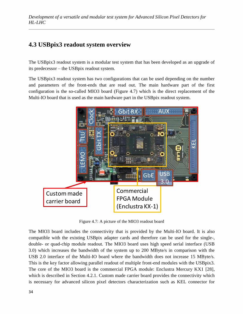
4.3 USBpix3 readout system overview
The USBpix3 readout system is a modular test system that has been developed as an upgrade of
its predecessor – the USBpix readout system.
The USBpix3 readout system has two configurations that can be used depending on the number
and parameters of the front-ends that are read out. The main hardware part of the first
configuration is the so-called MIO3 board (Figure 4.7) which is the direct replacement of the
Multi-IO board that is used as the main hardware part in the USBpix readout system.
Figure 4.7: A picture of the MIO3 readout board
The MIO3 board includes the connectivity that is provided by the Multi-IO board. It is also
compatible with the existing USBpix adapter cards and therefore can be used for the single-,
double- or quad-chip module readout. The MIO3 board uses high speed serial interface (USB
3.0) which increases the bandwidth of the system up to 200 MByte/s in comparison with the
USB 2.0 interface of the Multi-IO board where the bandwidth does not increase 15 MByte/s.
This is the key factor allowing parallel readout of multiple front-end modules with the USBpix3.
The core of the MIO3 board is the commercial FPGA module: Enclustra Mercury KX1 [28],
which is described in Section 4.2.1. Custom made carrier board provides the connectivity which
is necessary for advanced silicon pixel detectors characterization such as KEL connector for

4.4 Firmware, hardware and software of the USBpix3 readout system
35
Burn-In Card, FE-I4 Adapter Card and GPAC, connections for the trigger logic, connections for
the Gbit links, USB 3.0 and Ethernet connections. More detailed information regarding the
custom carrier board of the MIO3 is given in Section 4.4.2.1.
The main hardware part of the second configuration of the USBpix3 readout system is the so-
called MMC3 board (Figure 4.8) which allows direct connection of the FE-I4 modules. Thus no
FE-I4 Adapter or Burn-In Cards are needed. This is not possible with the USBpix readout
system.
Figure 4.8: A picture of the MMC3 readout board
The MMC3 board is a modification of the MIO3 board, where the KEL connector is replaced
with eight RJ-45 connectors with optional AC-coupling, that allow direct connection of the FE-
I4 modules. Differential drivers and receivers for clock, command and data lines in this case are
implemented in the FPGA firmware due to the fact that the USBpix adapter card which holds
LVDS transceivers is not used with the MMC3 board. Thus direct connection of up to eight or
more FE-I4 readout chips is possible depending on the clock and command lines sharing. The
AC-coupling option is needed, for example, for the Serially Powered Stave readout where each
module has different ground potential. Four additional power channels are available as well on
the MMC3 board. The rest of the connectivity is similar to the MIO3 board. The Enclustra
Mercury KX1 FPGA module is also used on the MMC3 board as a core. More detailed
information regarding the custom carrier board of the MMC3 is given in Section 4.4.2.2.
4.4 Firmware, hardware and software of the USBpix3 readout
system
A detailed block diagram showing developed firmware, hardware and software for the USBpix3
readout system can be seen on Figure 4.9. Only a brief overview of every block of the diagram is

Development of a versatile and modular test system for Advanced Silicon Pixel Detectors for
HL-LHC
36
given in a dedicated section below. A full description of the developed firmware, hardware and
software for the USBpix3 readout system can be found in Appendix.
Figure 4.9: A detailed block diagram showing developed firmware, hardware and software for the
USBpix3 readout system
4.4.1 Firmware of the USBpix3
4.4.1.1 USB 3.0 microcontroller firmware
Developed firmware for the USBpix3 includes the firmware for the so-called FX3 device [29]
which is a USB 3.0 microcontroller that includes an ARM CPU. The FX3 device is located on
the Enclustra Mercury KX1 FPGA module. The developed firmware connects the FPGA module
to a data acquisition computer (host) and is compatible to the existing software framework of the
USBpix readout system (pyBAR [30]).
Implementation of a USB 3.0 interface includes configuration of four endpoints for different
transfer types as well as USB enumeration descriptors in order to send data to the host and
receive data from it. Figure 4.9 shows the configured endpoints. Endpoints 2 and 6 are used for
block transfers in DMA auto channels that are implemented between USB endpoints and General
Programmable Interface (GPIF) sockets to maximise the transfer speed between the host and the
FPGA as these channels operate without CPU intervention. Endpoint 1 is used for control
transfers and slow peripherals such as I2C and SPI interfaces that are configured to allow
accessing EEPROM and SPI Flash on-board. I2C and SPI transfers use DMA manual channels
that are implemented as well and suppose CPU intervention.

4.4 Firmware, hardware and software of the USBpix3 readout system
37
Connectivity between the FX3 device and the FPGA is realized with the GPIF interface which is
integrated in the FX3 device (Figure 4.9) and can be configured by the means of state machine.
All the details concerning the GPIF interface itself as well as its configuration for the USBpix3
can be found in Appendix.
GPIF and FPGA timing parameters are taken into account during the firmware development.
Dedicated simulations with FX3 development software (GPIF II Designer) and with FPGA
development software (ISim) have been performed in order to verify the correct operation of the
interface.
4.4.1.2 FPGA firmware
The developed Kintex-7 FPGA firmware provides readout and configuration logic for pixel
readout chips and modules which is the main goal of the USBpix3 readout system. It provides
the connectivity to the FX3 device and includes DDR3 and Block RAM modules to buffer the
data from the front-end, PLL to generate the required clock signals for the design, registers and
user modules that are adapted from the USBpix readout system FPGA firmware (Basil [31]) in
order to support the new hardware (MIO3 and MMC3 boards) such as command sequencer and
receiver modules for the FE-I4, TLU (Trigger Logic Unit) module and arbiter module. The
developed FPGA firmware supports the readout of multiple front-ends and has dedicated
differential drivers and receivers for clock, command and data lines to and from the front-end (in
case of the MMC3 board). The implemented Kintex-7 FPGA firmware also provides the
connectivity to the USBpix adapter cards (in case of the MIO3 board) and a number of peripheral
connectors and interfaces that are described in detail in Section 4.4.2. The FPGA firmware is
organized in a modular structure where every module has its address space (Figure 4.9). A
detailed description of every implemented module is given in Appendix.
Structure and connections of the FPGA firmware modules are kept unified with the USBpix.
This means that coding principles and code structure are kept the same as in the FPGA firmware
for the USBpix system. Therefore, user willing to switch from the USBpix to the USBpix3 can
easily understand the modules structure and adjust it to his own needs.
4.4.2 Carrier boards for the USBpix3
4.4.2.1 MIO3

Development of a versatile and modular test system for Advanced Silicon Pixel Detectors for
HL-LHC
38
Figure 4.10 shows the top view of the PCB design of the MIO3 carrier board which has been
developed with the help of the Altium Designer software.
Figure 4.10: Top view of the PCB design of the MIO3 carrier board
This custom made carrier board holds a number of components and provides the connectivity
which is necessary for advanced silicon pixel detectors characterization such as KEL connector
(on the right side) for Burn-In Card, FE-I4 Adapter Card and GPAC, LEMO and RJ-45
connectors for the trigger logic (on the left side), SMA connectors for the external clock and the
Gbit links, USB-B 3.0 and Gigabit Ethernet connectors to provide connectivity to a data
acquisition computer. Schematic of the board can be found in [33]. A complete description of the
developed PCB design of the MIO3 carrier board, including all the components and possible
configurations of the board, can be found in Appendix.
The tracks for the MGTs (Multi-Gigabit Transceivers), USB 3.0 and Gigabit Ethernet are routed
according to the high speed PCB design requirements. All the differential tracks in the design are
routed according to the differential signaling requirements. Thus the signal integrity is
maintained.
4.4.2.2 MMC3
Figure 4.11 shows the top view of the PCB design of the MMC3 carrier board which has also
been developed with the help of the Altium Designer software.

4.4 Firmware, hardware and software of the USBpix3 readout system
39
Figure 4.11: Top view of the PCB design of the MMC3 carrier board
The MMC3 carrier board has the same connectivity as the MIO3 carrier board apart from the
KEL connector which is replaced with eight RJ-45 connectors with optional AC-coupling. This
allows direct connection of the FE-I4 modules. In the current FPGA firmware design each RJ-45
connector is an individual channel which includes differential clock, command, data and NTC
lines. The USBpix adapter card (FE-I4 adapter card or Burn-in card) which holds LVDS
transceivers is not used with the MMC3 and therefore differential drivers and receivers for clock,
command and data lines are implemented in the FPGA firmware in this case, allowing direct
connection of up to eight or more FE-I4 readout chips. The maximum number of the FE-I4
readout chips that can be readout with the MMC3 depends on the clock and command lines
sharing. Schematic of the board can be found in [33].
The AC-coupling option is needed for the serially powered stave readout where each module has
different ground potential. Dedicated solder jumpers (JP17 – JP24) can be configured for
differential clock and command lines to reduce the common mode voltage or set it to a certain
potential. This is needed in case of the FE-I4 readout and depends on the chosen LVDS coupling
option. Figure 4.12 shows FE-I4 specific LVDS coupling options that can be chosen on the
MMC3 carrier board.

Development of a versatile and modular test system for Advanced Silicon Pixel Detectors for
HL-LHC
40
Figure 4.12: FE-I4 specific LVDS coupling options that can be chosen on the MMC3 carrier board
A complete description of the developed PCB design of the MMC3 carrier board, including all
the components and possible configurations of the board, can be found in Appendix.
PCB design optimizations for the mass production versions of the MIO3 and the MMC3 carrier
boards have been performed. This includes schematic optimizations, routing optimizations for
the signal layers and the power planes. Placement optimizations are necessary in order to enable
more efficient routing. Unification of the components is performed as well. It supposes usage of
the same components for the common parts of the MIO3 and the MMC3 boards. A number of
user friendly optimizations are made as well. This includes the same placement of the
components for the common parts of the MIO3 and the MMC3 boards, additional holes for board
stability, mounting posts for the connectors between the carrier board and KX1 module,
footprints optimizations for easier soldering, better buttons, etc.
4.4.3 PyBAR readout framework adaptation to the USBpix3
4.4.3.1 PyBAR readout framework overview
PyBAR (Bonn ATLAS Readout in Python and C++) is a versatile test and readout framework for
the ATLAS FE-I4(A/B) pixel readout chip [30].

4.5 Performance and functionality tests for the USBpix3
41
Basil framework [31] is used by pyBAR for accessing the readout hardware. Basil is a modular
testing and data acquisition framework in Python which provides generic FPGA firmware
modules for different hardware platforms and drivers for wide range of lab appliances.
More detailed description of the PyBAR readout framework including all its main features and
functionality can be found in Appendix.
4.4.3.2 USBpix3 related PyBAR adaptations
The pyBAR software framework has been adapted to support the USBpix3 hardware and
firmware. In particular, multi-chip and multi-module readout support has been implemented for
the MIO3 and MMC3 boards, which is the major adaptation. This includes separate
configuration of the front-ends and separation of the output data. Existing scans dedicated for
single front-end chip readout have been transformed into parallel or consecutive scans for
multiple front-end chips where dedicated output files are generated for each front-end.
Possibility to disable single command channel has been added as well for the case when multiple
front-ends with identical addresses should be configured with individual configurations. This is
the case for the serially powered stave readout.
Currently various tests, scans and tunings can be performed with USBpix3 and pyBAR for
multiple front-ends:
Global and pixel register tests
IV, digital, analog, threshold, source, double trigger, external trigger and self-trigger
scans
Threshold, gain, noise occupancy, minimum threshold and threshold baseline tunings
Online monitoring
More detailed information concerning the USBpix3 related PyBAR adaptations is provided in
Appendix.
4.5 Performance and functionality tests for the USBpix3
4.5.1 USB 3.0 microcontroller and FPGA firmware tests
Dedicated tests have been made in order to verify the performance of the developed USB 3.0
microcontroller and FPGA firmware.

Development of a versatile and modular test system for Advanced Silicon Pixel Detectors for
HL-LHC
42
A speed test is essential in order to verify that the full potential of the USB 3.0 interface is used
for the implemented data transfer between the host and the FPGA. Thus, the speed test has been
performed for the developed firmware, where the data transfer was realized between the host and
the Block RAM of the FPGA by the means of the FX3 device. Figure 4.13 shows the results of
this test and the maximum transfer speed that is reached between the host and the FPGA during
reading from the FPGA (≈ 280 Mbyte/sec = 2.24 Gbit/sec) and writing to the FPGA (≈ 75
Mbyte/sec = 0.6 Gbit/sec). Achieved speeds exceed the ones of the USBpix readout system by a
factor of 18 and, therefore, allow using the USBpix3 for the multi-chip pixel modules, multiple
pixel modules (e.g. FE-I4 based quad modules) and next generation of front-ends readout (e.g.
RD53 readout chip).
Figure 4.13: The results of the speed test for the developed firmware, where the data transfer was realized
between the host and the Block RAM of the FPGA by the means of the FX3 device
The speed test has also been performed with the help of the so called “Streamer” application
provided by Cypress (the manufacturer of the FX3 device), which is intended to demonstrate the
maximum speed of the FX3 device. The data transfer in this case was realized between the host
and the FX3, independently from the FPGA in order to prove that the data transfer between the
FX3 device and the FPGA doesn’t cause a bottleneck between the host and the FPGA. Maximum
achieved reading speed is ≈ 286 Mbyte/sec and maximum achieved writing speed is ≈ 78
Mbyte/sec. These values are in a good agreement with the ones achieved with the developed
USB 3.0 microcontroller and FPGA firmware (Figure 4.13). This confirms that the implemented
data transfer between the host and the FPGA uses the full potential of the USB 3.0 interface and
no bottlenecks have been created in the developed USB 3.0 microcontroller and FPGA firmware.
The speed test is essential but not sufficient to fully verify the USB 3.0 microcontroller and
FPGA firmware. The data integrity test is essential as well in order to prove that the data
integrity is maintained during the implemented data transfer between the host and the FPGA.
This test has been performed. The data transfer was realized between the host and the Block
RAM of the FPGA by the means of the FX3 device. Various sizes of blocks with randomly
generated data were written from the host via the FX3 device to the Block RAM of the FPGA,
read back by the FX3 device and transferred back to the host where the data integrity was

4.5 Performance and functionality tests for the USBpix3
43
verified. The data integrity test proved that no data integrity errors appear during the data transfer
between the host and the FPGA.
Thus the speed and the data integrity tests have been successfully performed for the developed
USB 3.0 microcontroller and FPGA firmware. The results of these tests prove that the developed
firmware is stable and functions at the maximum possible performance defined by the hardware.
4.5.2 Hardware design tests
Hardware design tests for the USBpix3 readout system were performed prior to the mass
production. The goal of these tests is to verify the functionality of the developed design and to
prove the operability and expected performance of the design components. Performed tests
include tests for the MGTs and clocking resources, Ethernet, USB 3.0, KEL, JTAG, triggering,
powering and other components.
A loopback test has been performed for the MGTs and the clocking resources on the MIO3
prototype board with the help of the customizable LogiCORE™ IP Integrated Bit Error Ratio
Test (IBERT) core for 7 series FPGA MGT transceivers which is designed for evaluating and
monitoring the MGT transceivers [45]. This test is essential to prove that the MGTs and the
clocking resources can be used reliably for the readout and characterization of the next
generation front-ends that are currently being developed for the ATLAS ITk pixel detector (i.e.
RD53 readout chip) and require the readout system to support multiple Gigabit serial links.
Enclustra Mercury KX1 FPGA module includes 4 multi-gigabit transceivers (MGTs) that are
part of Kintex 7 FPGA. 4 multi-gigabit transceivers compose a so-called MGT Quad where 4
channels share 1 common PLL. Each channel includes a channel PLL, a transmitter and a
receiver. These transceivers support line rates up to 10 Gb/s and are needed for the
characterization of the future RD53 readout chips. MIO3 carrier board supports usage of 2
MGTs. For that purpose it holds reference clock oscillator for MGTs, 2 SMA connectors for
external reference clock and 8 SMA connectors for differential channels of 2 transmitters (TXs)
and 2 receivers (RXs). Thus there are two possible sources of the reference clock for the MGTs.
The first one is the reference clock oscillator, located on the carrier board. It has a startup
frequency of 156.25 MHz that can be used as a reference clock for the MGTs. This frequency
can be reprogrammed to another value via the I2C interface. The clock fanout buffer duplicates
the reference clock signal. The first output of the fanout buffer is fed directly to the reference
clock input 1 of the FPGA MGT Quad. The second output of the fanout buffer is connected to
the clock multiplexer. The output of the clock multiplexer is connected to the reference clock
input 0 of the FPGA MGT Quad. Therefore the reference clock input 0 can use either the
reference clock signal provided by the reference clock oscillator or the external reference clock

Development of a versatile and modular test system for Advanced Silicon Pixel Detectors for
HL-LHC
44
provided via two SMA connectors. The schematic of the reference clock generation for the
MGTs is shown on Figure 4.14.
Figure 4.14: Schematic of the reference clock generation for the MGTs
Channel 0 of the MGT Quad was used for the test in order to fully verify the clocking resources
including the clock multiplexer, which is bypassed if channel 1 is used. Reference clock
oscillator from the carrier board was used as a source of the reference clock for the MGT Quad
(Figure 4.14). Transmitter differential lines (TX0 P/N lines) were connected with corresponding
receiver differential lines (RX0 P/N lines) of this channel (Figure 4.15).

4.5 Performance and functionality tests for the USBpix3
45
Figure 4.15: The MIO3 prototype board during the MGTs test
The loopback test was running for about 4 hours at a line rate of 3.125 Gb/sec. Quad and channel
PLLs of the MGT Quad were locked. 7-, 15-, 23- and 31-bit pseudorandom binary sequence
(PRBS) patterns have been tested. No bit errors have been registered. Figure 4.16 shows the
result of the loopback test. The open area of the 2D full eye scan looks as expected. It is defined
as the area which has the same amount of errors in both dimensions as the center (no errors) [46].
The units are in Unit Intervals in the time domain and Codes in the Voltage scale. Codes are a
unit-less dimension since this is after the equalizer and there is no way to correlate voltage at the
pins, and the offset codes that are used to control this value. The colours in the hit map are the
number of errors at a certain point. The width (≈ 0.624 Unit Intervals) and the height (≈ 140
Codes) of the open area fully conform to the receiver requirements of the MGT. These results
prove that the MGTs and the clocking resources of the USBpix3 readout system can be reliably
used for the readout and characterization of the RD53 readout chips.

Development of a versatile and modular test system for Advanced Silicon Pixel Detectors for
HL-LHC
46
Figure 4.16: The 2D full eye scan of the loopback test
Ethernet is an alternative to the USB 3.0 interface on the USBpix3 readout system. It can be used
to provide connection to the host. However in this case the maximum bandwidth of the system
will decrease to ≈ 1 Gbit/sec with respect to ≈ 2.24 Gbit/sec achieved with the USB 3.0 interface.
Nevertheless it is needed for the applications where large distance is required between the host
and the USBpix3.
The Ethernet functionality has been tested on the MMC3 prototype board (Figure 4.17). This is
essential in order to verify that the Ethernet option for providing connection to the host works
reliably.
Figure 4.17: The MMC3 prototype board during the Ethernet test

4.5 Performance and functionality tests for the USBpix3
47
The Xilinx Embedded Development Kit (EDK) reference design from Enclustra has been used as
a software and firmware for the Ethernet test. It includes pre-synthesized FPGA-bitstream along
with some demonstration applications. The block diagram of the design shows the FPGA
firmware (in light blue) as well as the connected peripherals on the Mercury FPGA module and
the MIO3/MMC3 boards (Figure 4.18). The reference design allows testing the functionality of
various peripherals.
Figure 4.18: The block diagram of the Xilinx Embedded Development Kit (EDK) reference design from
Enclustra [28]
During the test the MMC3 prototype board was connected to the host via Ethernet. A loopback
test has been made using PuTTY and an embedded Telnet Echoserver. Every character sent to
the Mercury KX1 was immediately sent back. The loopback test proved that no data integrity
errors appear during the data transfer between the host and the USBpix3 via Ethernet.
Embedded webserver functionality of the USBpix3 has been verified as well during the Ethernet
test. A Xilinx WebServer Demo web page allows controlling LEDs on the MMC3 via an Internet
browser with the help of the embedded webserver. The LEDs were successfully toggled and the
state of the LEDs was correctly shown on the web page. Thus the embedded webserver
functionality can be used with the USBpix3 readout system and can provide a method to control
and monitor it via an Internet browser.
The Ethernet test proves that the Ethernet option for providing connection between the USBpix3
and the host works reliably and can be used for the applications where large distance is needed

Development of a versatile and modular test system for Advanced Silicon Pixel Detectors for
HL-LHC
48
between the host and the readout system as well as for the applications where the readout system
is desired to be monitored and controlled via Internet.
Functionality verification for the other hardware components of the USBpix3 has been
performed during the various characterization measurements of the FE-I4 based single- and
multi-chip modules. All the other hardware components of the developed design of the USBpix3
function as expected.
The results of all the performed hardware design tests for the USBpix3 readout system ensure the
expected functionality of the developed design as well as the operability and expected
performance of the design components.
4.5.3 Configuration and testing prior to distribution
Prior to distribution the MIO3 and MMC3 boards are configured with dedicated jumpers
described in detail in Appendix. The set configuration is intended for the readout of single or
multiple FE-I4 based modules.
Apart from the tests described in Section 4.5.2 a digital scan of the FE-I4 readout chip (see
Section 4.6.1) is performed with every board prior to distribution in order to fully verify its
functionality which is needed for the front-end characterization.
Up to now 60 MMC3 and 20 MIO3 boards have been produced, tested and distributed to many
groups in ATLAS, CMS, Belle II and other collaborations [62]. These numbers are expected to
grow in the future. Broad functionality available for the characterization of advanced silicon
pixel detectors along with high bandwidth, light weight and small size make the USBpix3
readout system highly popular in the LHC collaboration and beyond.
4.6 Performance with FE-I4 chips and modules
The developed USBpix3 readout system has been used to characterize single and quad FE-I4
modules functionalities. The results of the measurements demonstrate the performance of the
USBpix3 and verify whether the tested single and quad FE-I4 modules function correctly. All the
measurements shown in Section 4.6.1 have been performed with modules powered according to
the standard voltage-based powering scheme and are used as one of the references for the
measurement results of the serially powered modules described in Section 6.3. The
measurements described in Section 4.6.2, where the modules were powered in a so-called shunt-

4.6 Performance with FE-I4 chips and modules
49
LDO mode which is described in detail in Section 5.3.1, have been performed as a part of the
quad modules preparation and qualification for the serially powered stave and are used as an
additional reference.
4.6.1 Characterization of single FE-I4 chip functionalities with the USBpix3
Several test charge injection circuitries are available per pixel in the FE-I4 (Figure 3.8). These
circuitries are used for measurements of the analog and digital performance of the front-end. The
calibration voltage (Vcal) and two test charge injection capacitances (Cinj1, Cinj2) define the
voltage step of the injected analog test signal which allows testing the analog pixel region of the
FE-I4 by injecting a high charge. Cinj1 and Cinj2 can be used together or separately. The following
formula is used for the injected charge calculation:
Q [e] = Cinj[F] × Vcal[V] × 1/e[C], (4.1)
where e is the elementary charge.
The main source of error for the performed measurements comes from the calibration of the
injected charge, and it is calculated to be ~5 %.
The output of the discriminator of every pixel in the FE-I4 is ORed with the digital test injection
input (DigHit) that can be used as well as analog test signals for the characterization of the front-
end. The digital test injection input allows testing the digital functionality of the front-end
excluding the analog pixel region. The digital test injection can be disabled with the help of the
Dig_En input which is connected with the DigHit input via a logical AND. The AND element
that is connected to the enable bit (EN) and the output of the discriminator allows disabling the
output of the analog readout chain of every pixel.
These charge injection circuitries have been used for the so-called FE-I4 analog and digital scans
that have been performed with the developed USBpix3 readout system and the adapted pyBAR
software. Figure 4.19 shows a picture of the setup that has been used to characterize single FE-I4
module functionalities. The MIO3 prototype board connected to the FE-I4 Adapter Card is used
as a USBpix3 readout hardware. The FE-I4 readout chip bump bonded to an n-in-n silicon planar
sensor 200 µm thick is located on the Single Chip Card which is connected to the FE-I4 adapter
card. An external power supply provides the necessary voltages for the FE-I4 readout chip. The
required bias voltage is provided for the sensor as well.

Development of a versatile and modular test system for Advanced Silicon Pixel Detectors for
HL-LHC
50
Figure 4.19: The setup that has been used to characterize a single FE-I4 module: The MIO3 prototype
board connected to the FE-I4 Adapter Card, the Single Chip Card with the FE-I4 readout chip, bump
bonded to an n-in-n silicon planar sensor 200 µm thick, and an external power supply
During the analog scan a large test charge several times higher than the threshold is injected to
each pixel of the FE-I4 pixel matrix with the help of the calibrated test charge injection circuitry.
Figure 4.20a shows the result of this scan which is a hit map with the occupancy of each pixel.
100 injections with a charge corresponding to ~16 ke- at a threshold of ~1500 e
- have been
performed into each pixel. A well working pixel array with only 5 pixels (0.02 % of all pixels)
not responding can be seen on this FE-I4 readout chip. This result is identical to the one obtained
with the help of the USBpix readout system for the same front-end proving that no errors are
added by the developed USBpix3 readout system.
Figure 4.20: Hit map with the occupancy of each pixel of the FE-I4 pixel matrix for the analog scan (a)
and the digital scan (b)
Single Chip Card
MIO3 prototype board FE-I4 Adapter Card

4.6 Performance with FE-I4 chips and modules
51
A digital scan has been performed as well in order to separate the errors in the analog readout
chain from the errors in the digital readout chain. Digital test hit injection circuitry has been
used. Figure 4.20b shows the result of this scan which is a hit map with the occupancy of each
pixel. 100 digital test hit injections have been performed into each pixel. All the pixels show an
occupancy which is the same as the number of injected test hits proving the absence of the errors
in the digital readout chain. An identical result has been obtained with the USBpix readout
system for this front-end.
Detector operation and data reconstruction require a uniform ToT and threshold response over
the full pixel matrix. Process variations lead to a wide distribution of the feedback currents and
thresholds over the pixel matrix. The threshold distribution of the un-tuned FE-I4 readout chip is
shown on the Figure 4.21a. The width of a Gaussian fit to the threshold distribution is ~ 330 e-.
The large width of the distribution indicates the need to adjust the threshold at the pixel level.
Figure 4.21: The threshold distribution of an un-tuned FE-I4 readout chip (a). The need to adjust the
threshold at the pixel level is indicated by the large width of the distribution due to production variations.
The mean ToT response distribution of an un-tuned FE-I4 readout chip to test charge injections of ~16 ke-
(b). The need to tune the feedback current at the pixel level is indicated by the broad distribution of the
ToT bins.
Figure 4.21b shows the mean ToT response distribution of the un-tuned FE-I4 readout chip to
test charge injections of ~16 ke-, which corresponds to the most probable charge generated by a
minimum ionizing particle (MIP) in the sensor. The pixels respond with a mean ToT between 6
and 13, which is more than half of the dynamic ToT range of the chip. The charge information
cannot be used for the experiment in this case, therefore it is necessary to perform the feedback
current adjustment at the pixel level.
The feedback current and threshold can be set globally and at the pixel level in the FE-I4 as
described in Section 3.6.2. The USBpix3 readout system uses adapted tuning algorithm of

Development of a versatile and modular test system for Advanced Silicon Pixel Detectors for
HL-LHC
52
pyBAR in order to perform the feedback current and threshold adjustments, which is an iterative
process because they influence each other. The so-called IBL target values (given below) for
tuning have been used. These values are used for the operation of the IBL modules in the pixel
detector of the ATLAS experiment [47]. The threshold setting in this case is the most optimal
value between the need to have a low noise hit occupancy, which is required to avoid fake hits
degrading the performance of the pattern recognition algorithms, and the need to have a high
enough signal above the threshold, which is required for a high hit detection efficiency. The
feedback current setting is the most optimal value between the need to detect large charges due
to the high charge tail in the Landau distribution and the need to allow the resolution of small
hits due to charge sharing between neighbouring pixels. Thus the feedback current of the pre-
amplifier and the discriminator threshold have been tuned over the entire pixel matrix and for
each pixel. The target threshold is 1500 e-. The feedback current is tuned in such a way that a
return to baseline within 250 ns (10 ToT) is obtained for a signal corresponding to 16 ke-. Figure
4.22 shows the results of the tuning of the FE-I4 readout chip: the threshold distribution (Figure
4.22a) and the mean ToT distribution (Figure 4.22b). The threshold distribution after tuning
looks as expected: it is uniform and centered around the target value. The width of the threshold
distribution is reduced to the minimum achievable width with the TDAC step width of about 30
e-. The width of a Gaussian fit to the threshold distribution after tuning is ~ 30 e
- compared to ~
330 e- width of a Gaussian fit to the threshold distribution before tuning.
Figure 4.22: The threshold distribution of the FE-I4 after tuning (a). The width of a Gaussian fit to the
threshold distribution after tuning is reduced significantly to ~ 30 e- compared to ~ 330 e
- width of a
Gaussian fit to the threshold distribution before tuning. The error on the threshold value in electrons is
around 5% and comes from the calibration of the injection circuit, disregarding any offset. The mean ToT
response distribution of the tuned FE-I4 readout chip to test charge injections of ~ 16 ke- (b). The width of
the mean ToT response distribution is reduced significantly with almost all pixels responding with the
target ToT of 10.

4.6 Performance with FE-I4 chips and modules
53
The mean ToT response distribution of the tuned FE-I4 readout chip to test charge injections of ~
16 ke- looks as expected as well and is centered around the target value. The width of the mean
ToT response distribution is reduced significantly. Almost all pixels respond with the target ToT
of 10.
FDAC and TDAC distributions after tuning indicate the quality of tuning as well. They should be
Gaussian distributed around the central value and cover the full dynamic range in ideal case after
tuning. The FDAC and the TDAC distributions of the FE-I4 after tuning are shown on the Figure
4.23. They look as expected: centered around the central value of the DAC setting and well
homogenous. Slight top-to-bottom variations across the front-end come from the supply voltage
variations from the power distribution network.
Figure 4.23: TDAC (a) and FDAC (b) distributions after the successful tuning of the FE-I4 readout chip
An important characteristic of the analog pixel cell is the electronic noise (ENC), which is
defined as the equivalent amount of charge at the input node of the amplifier chain resulting in a
signal of equal amplitude as the ENC. Section 3.6.2.1 contains more details concerning the
expected ENC in the FE-I4. The noise distribution of the FE-I4 readout chip after tuning to the
IBL target values performed with the USBpix3 readout system is shown on the Figure 4.24a.
Figure 4.24b shows the noise distribution for the same chip after tuning performed with the
USBpix readout system as an example. No significant difference in distributions is observed
proving that no additional noise is added by the USBpix3. The noise is uniformly distributed
over the whole chip. As predicted by the calculations described in Section 3.6.2.1 the mean value
of the ENC is ~130 e-.

Development of a versatile and modular test system for Advanced Silicon Pixel Detectors for
HL-LHC
54
Figure 4.24: The noise distribution of the FE-I4 readout chip after tuning to the IBL target values
performed with the USBpix3 readout system (a) and with the USBpix readout system (b)
All the obtained results of the threshold and ToT distributions before and after tuning as well as
the TDAC, FDAC and noise distributions after tuning for this FE-I4 readout chip are in a very
good agreement with the results of the same measurements performed with the USBpix readout
system for this chip proving that the USBpix3 readout system functions correctly.
A special signal called HitOR is available in every pixel of the FE-I4 readout chip in order to be
able to use it in a self-trigger mode (Figure 3.8). A pull-down transistor and a logical OR are
used to connect the output (HitOut) of every pixel with the global HitOR bus. This allows using
the HitOR bus for triggering because it will go low if the output of any discriminator is high. The
inverter in the front-end’s periphery in the end makes the HitOR signal active high at the wire
bond pad.
The self-trigger mode of the FE-I4 readout chip has been used for the source scan. This scan
records hits from a radioactive source. Thus the trigger signal in this case is generated by the
front-end every time a hit is recorded. The source scan allows verifying the complete
functionality of the readout chip from charge collection in the sensor to hit processing in the
front-end and data outputting. The source used for this test is an 241
Am source. A fraction of low
energy gamma rays emitted by the 241
Am source is absorbed by atomic electrons that are hence
moved into the conduction band due to the photoelectric effect that is the dominant process at
low photon energies, in silicon below about 100 keV as shown on the Figure 3.2 in the Section
3.5 [13]. The noise occupancy and stuck pixel tunings have been performed prior to the source
scan in order to mask noisy and stuck pixels. Noisy pixels have to be removed due to the fact that
they affect the recorded hit map and ToT distribution. Stuck pixels keep the HitOR signal
constantly active high and thus have to be removed in order to enable self-triggering mode. The
recorded hit map is shown on the Figure 4.25a. A higher number of hits corresponds to the
(a) (b)

4.6 Performance with FE-I4 chips and modules
55
source location as expected. The ToT distribution is shown on the Figure 4.25b. The peak in the
distribution corresponds to a charge of ~16 ke-. The charge resolution of the FE-I4 readout chip
is limited by the 4 available bits for the ToT code. The error on the calibration of the injected
charge is about 5 %. The charge of ~16 ke- corresponds to an energy of ~57.6 keV which is in a
very good agreement with the 60 keV peak of the 241
Am source spectrum. This result proves that
the FE-I4 readout chip functions correctly from charge collection in the sensor to hit processing
in the front-end and data outputting. The source scan result for this FE-I4 readout chip is in a
very good agreement with the result of the source scan performed with the USBpix readout
system for this chip (Figure 4.26).
Figure 4.25: The recorded hit map of the source scan (a). The ToT distribution of the source scan (b). 241
Am source was used. Readout with the USBpix3.
Figure 4.26: The recorded hit map of the source scan (a). The ToT distribution of the source scan (b). 241
Am source was used. Readout with the USBpix.
Thus all the main functionalities of the single FE-I4 readout chip have been tested with the
USBpix3 readout system. The obtained results prove that the tested FE-I4 readout chip functions
(a) (b)
(a) (b)

Development of a versatile and modular test system for Advanced Silicon Pixel Detectors for
HL-LHC
56
correctly. Moreover these results have been obtained with the FE-I4 powered according to the
standard voltage-based powering scheme and are used as one of the references for the
measurement results of the serially powered modules described in Section 6.3.
All the results are in a very good agreement with the results obtained with the USBpix readout
system and therefore prove the correct operation of the USBpix3. Thus the USBpix3 readout
system can be used for the full characterization of single FE-I4 readout chips.
4.6.2 Characterization of quad FE-I4 module functionalities with the USBpix3
Parallel readout of all the front-ends on the quad module is only possible with the USBpix3
readout system and not possible with the USBpix readout system due its limited data throughput.
Quad module readout requires the readout system to cope with the 80 Mbyte/s data rate and the
USBpix system, which was developed mainly for single front-end chip support, is only capable
of 15 Mbyte/s data rate that is determined by the USB 2.0 interface. The USBpix3 readout
system meets and exceeds these requirements and can cope with the data rates of up to 280
Mbyte/s as shown in Section 4.5.1. This allows using the USBpix3 for the readout of multiple
quad modules as it is shown in Chapter 6.
The performance of the USBpix3 readout system during the quad module readout has been
verified. Several FE-I4 quad modules have been characterized standalone with the help of the
USBpix3 readout system and the adapted pyBAR software as a part of the quad modules
preparation and qualification for the serially powered stave described in Section 6.2. Figure 4.27
shows a picture of the setup that has been used to characterize FE-I4 quad modules
functionalities. The MMC3 board connected to the quad module adapter PCB is used as a
USBpix3 readout hardware. The shown FE-I4 quad module (called BNQ02) consists of the 4
readout chips bump bonded to an n-in-n silicon planar sensor of 200 µm thickness. A flexible
printed circuit board (module flex) is glued on the sensor. Connection between the module flex
and the readout chips is realized with the help of wire bonds. The module flex is used to provide
the connectivity to the quad module adapter PCB. An external power supply provides the
necessary constant current for the FE-I4 quad module which is powered in a so-called shunt-
LDO mode which is used for the quad modules on the stave and described in detail in Section
5.3.1. The bias voltage for the sensor is provided externally as well. The quad module is located
in a climate chamber that keeps the temperature at 18 C assuring a module temperature of 35
C
during operation.

4.6 Performance with FE-I4 chips and modules
57
Figure 4.27: The readout used for the quad module: MMC3 and pyBAR (a). Quad module adapter PCB
connected with the FE-I4 quad module in a climate chamber to cool down the module (b).
The sensor performance of the several quad modules has been verified. The current as a function
of the bias voltage is an important indicator of the sensor performance. In order to characterize
the sensor it is also necessary to detect the breakdown voltage. The measured leakage current as
a function of the bias voltage for the sensor of the BNQ02 quad module as an example is shown
on the Figure 4.28. The operation voltage of this planar sensor is -80 V and the full depletion is
reached at -50 V. Thus the obtained I-V curve proves that the sensor can be used for the modules
on the serially powered stave.
Figure 4.28: The measured leakage current as a function of the bias voltage for the sensor of the BNQ02
quad module
(a) (b)

Development of a versatile and modular test system for Advanced Silicon Pixel Detectors for
HL-LHC
58
A number of measurements have been performed for several FE-I4 quad modules. More detailed
explanations of the measurements concepts and the chip functionalities used can be found in
Section 4.6.1. Figure 4.29 shows the result of the analog scan performed for the BNQ02 quad
module as an example, which is a hit map with the occupancy of each pixel. 100 injections with
a charge corresponding to ~16 ke- at a threshold of ~1500 e
- have been performed into each
pixel. A well working pixel array with only 12 pixels (0.04 % of all pixels) in the worst case not
responding can be seen on this FE-I4 quad module for every front-end.
Figure 4.29: Hit map of the analog scan with the occupancy of each pixel of the FE-I4 pixel matrix for
every front-end on the BNQ02 quad module
A digital scan has been performed as well in order to separate the errors in the analog readout
chain from the errors in the digital readout chain. Digital test hit injection circuitry has been
used. Figure 4.30 shows the result of this scan which is a hit map with the occupancy of each
pixel. 100 digital test hit injections have been performed into each pixel. Only 1 pixel (out of
26880) in the worst case showed an occupancy which is different from the number of injected
test hits due to the errors in the digital readout chain.
FE1 FE2
FE3 FE4

4.6 Performance with FE-I4 chips and modules
59
Figure 4.30: Hit map of the digital scan with the occupancy of each pixel of the FE-I4 pixel matrix for
every front-end on the BNQ02 quad module
The feedback current of the pre-amplifier and the discriminator threshold have been tuned over
the entire pixel matrix and for each pixel of every front-end on the BNQ02 quad module. The
IBL target values have been used for tuning (see Section 4.6.1). Thus the target threshold is 1500
e-. The feedback current is tuned in such a way that a return to baseline within 250 ns (10 ToT) is
obtained for a signal corresponding to 16 ke-. Figure 4.31 shows the results of the tuning of the
BNQ02 quad module: the threshold distribution (Figure 4.31a) and the mean ToT distribution
(Figure 4.31b). The threshold distribution after tuning looks as expected: it is uniform and
centered around the target value. The width of a Gaussian fit to the threshold distribution after
tuning is below 30 e-. The mean ToT response distribution of the tuned quad module to test
charge injections of ~ 16 ke- looks as expected as well and is centered around the target value.
Almost all pixels respond with the target ToT of 10.
FE1 FE2
FE3 FE4

Development of a versatile and modular test system for Advanced Silicon Pixel Detectors for
HL-LHC
60
(a)
(b)
Figure 4.31: The threshold distribution of every front-end on the BNQ02 quad module after tuning (a).
The width of a Gaussian fit to the threshold distribution after tuning is below 30 e- for every front-end.
The error on the threshold value in electrons is around 5% and comes from the calibration of the injection
circuit, disregarding any offset. The mean ToT response distribution of every front-end on the BNQ02
quad module after tuning to test charge injections of ~ 16 ke- (b). Almost all pixels respond with the target
ToT of 10.
FE1 FE2
FE3 FE4
FE1 FE2
FE3 FE4

4.6 Performance with FE-I4 chips and modules
61
The noise distribution of every front-end on the BNQ02 quad module after tuning to the IBL
target values is shown on the Figure 4.32. The noise is uniformly distributed over the whole chip
for every front-end. The obtained mean values of the ENC are in agreement with the calculations
described in Section 3.6.2.1.
Figure 4.32: The noise distribution of every front-end on the BNQ02 quad module after tuning to the IBL
target values
Thus all the main functionalities of several FE-I4 quad modules, powered in a shunt-LDO mode,
have been tested with the USBpix3 readout system as a part of the quad modules preparation and
qualification for the serially powered stave described in Section 6.2. The obtained results prove
that the tested quad modules function correctly. Even though only the results for the BNQ02
quad module are shown the results for all the other tested quad modules are in agreement with
the presented results. These results are used as one of the references for the measurement results
of the serially powered modules described in Section 6.3.
It also has been verified that the USBpix3 readout system can be used for the full
characterization of FE-I4 quad modules. Chapter 6 proves that the parallel readout of multiple
FE-I4 quad modules is supported by the USBpix3 readout system as well.
FE1 FE2
FE3 FE4

Serial powering scheme
62
Chapter 5
Serial powering scheme
One of the main challenges for the ATLAS ITk Phase II Pixel upgrade is a low-mass, efficient
power distribution for detector modules. This requires a powering scheme alternative to the
parallel (direct) powering which is currently used. A serial powering scheme has been chosen as
baseline for the ITk pixel system.
5.1 Motivation for serial powering in ATLAS
A large number of cables is needed to provide power, data and control signals to the pixel
detectors due to their high granularity (Figure 5.1a). Therefore service cables are one of the most
significant contributions to the material budget of the pixel detectors. The contribution of the
services is especially significant at large η (e.g. about 2 X0 at η=3) due to the concentration of
cables at the end of the end-caps and of the barrel, where they are the dominant source of
material as can be seen on the Figure 5.1b. This results into unwanted interactions of particles
with the inactive part of the detector and degradation of the performance of subsequent detectors.
Figure 5.1: Services of the ATLAS pixel detector (a). Material distribution for the current ATLAS tracker
(b) [10].
(a) (b)

5.1 Motivation for serial powering in ATLAS
63
The current ATLAS pixel detector modules are powered according to the parallel (direct)
powering scheme: each detector module is powered with an independent power supply and a set
of cables. 76 % of the cable material budget in the active area consists of the power cables. Low
voltage power cables to distribute power to the front-end electronics dominate the material
budget of the services of the pixel detector. Typical power density for the pixel detector is in the
order of kW/m2. With the parallel powering scheme modules can be operated individually, which
is a big advantage. However, due to foreseen increased granularity of the detector more cables
are needed for powering. Cable cross section has to be as small as possible to reduce the cable
volume within the detector active area due to the space constraints and low material budget
requirements. For a transmitted current I over a length l of a cable with the electrical
conductivity of the conducting material k and a voltage drop Vdrop on the cable the cable cross-
section A can be calculated according to the following formula:
𝐴 = 𝑙 ×𝐼
𝑉𝑑𝑟𝑜𝑝×
1
𝑘 (5.1)
According to the formula in order to keep the cable cross section as small as possible a high
voltage drop has to be allowed because high current has to be transmitted to the detector
modules. This leads to high power losses on the cables that equal Vdrop × I. The power losses
significantly reduce efficiency and produce a large amount of heat which increases the
requirements for the cooling systems. Additionally the cable cross section cannot be minimized
as it is required because the maximum allowed voltage drop is constrained to prevent over-
voltage across the modules in case of an abrupt current drop on the power line. Thus foreseen
increased front-end current consumption still leads to increase in cable cross section which
increases the amount of passive material in the active detector volume.
Every module in the current ATLAS pixel detector (except the IBL) consumes approximately 2
A and is powered with the digital and analog voltages required by the front-end that are 2.0 V
and 1.6 V. For a total power consumption of 6 kW the total current consumption of the pixel
detector is 3.7 kA [5]. The power efficiency is only 20 % due to the fact that 30 kW of power has
to be provided and the power losses in the cables equal to 24 kW. The voltage drop in the cables
is 6.4 V.
Thus the parallel (direct) powering schemes cannot be used at the HL-LHC where significantly
increased granularity and current are required to cope with the increased particle rate. The usage
of direct powering schemes for the pixel detectors at the HL-LHC would result in an
unacceptable amount of cables in terms of material budget and efficiency below 10 %. The
solution is the usage of a new powering scheme, different from the direct powering. Proposed
options are serial powering and a DC-DC converters scheme [48], [49]. These powering schemes
distribute power at low current and high voltage and can match the requirements of power
distribution at the HL-LHC [50].

Serial powering scheme
64
In the DC-DC converters scheme power is distributed at higher voltage and is then converted
close to the modules by switched DC-DC converters to the needed supply voltage. Standard buck
converters use coils with ferrite core that would be saturated in the magnetic field of the pixel
detector. Air coils with the same inductance are much bigger in size and are not compatible with
the need to reduce the amount of material used in the pixel detector.
The serial powering scheme has been chosen as the baseline for the ITk pixel system as this and
previous research projects [51], [52], [53] show that it can be reliably used to power detector
modules. It reduces power losses in the cables, cable material, total detector power consumption
and number of power supply channels and therefore increases power efficiency and reduces
material budget and costs.
5.2 Serial powering concept
In a serial powering scheme detector modules are placed in series and powered with a constant
current source. In this way power can be transmitted at low current and high voltage. The
reduction factor of the transmitted current is equal to the number of modules in a serial powering
chain as shown on Figure 5.2a. Figure 5.2b shows a parallel powering connection of the modules
which is currently used in the pixel detector.
Figure 5.2: Block diagram showing a general concept of a serial powering scheme (a). Block diagram
showing a general concept of a parallel powering scheme (b).

5.2 Serial powering concept
65
Thus in a serial powering scheme power is supplied to n modules using a constant current I. The
ground of each module is connected to the power input of the next module. A supply voltage
generation from the current supply to provide the digital and analog voltages needed by the
front-end electronics is performed at the module level with special on-chip regulators discussed
in detail in Section 5.3.1. The voltage across the serial powering chain is n × V, where the
voltage across the module V is the voltage at the input of the regulator. I is the transmitted
current which is set at the current supply. It is a sum of the current needed by the regulator and
the maximum current needed by the module.
A serial powering scheme is beneficial in comparison with a direct powering scheme due to the
fact that in a serial powering scheme only 2 cables and 1 power supply are needed for a number
of modules n. Powering efficiency is improved as well. If the inefficiency caused by the
regulation circuitry is neglected the improvement in powering efficiency of a serial powering
scheme is given by:
𝑉×𝐼
𝑉×𝐼 + 𝑅×𝐼2
𝑛
(5.2)
while the powering efficiency of a direct powering scheme is given by:
𝑉×𝐼
𝑉×𝐼 + 𝑅×𝐼2 (5.3)
R is the cable resistance, I is the current needed by n modules, V is the voltage across a module
and n is the amount of powered modules.
Thus power losses in an ideal serial powering scheme (𝑅×𝐼2
𝑛) are reduced by the number of
modules n in a serial powering chain with respect to the power losses in a direct powering
scheme (𝑅 × 𝐼2). Cable cross section in a serial powering scheme (𝐴
𝑛) is reduced as well by the
number of modules n in a serial powering chain with respect to the cable cross section in a direct
powering scheme (𝐴). All these lead to a total increased powering efficiency and reduced cable
volume.
However it has to be mentioned that the power dissipation of the modules in a serial powering
scheme is higher on average than in a direct powering scheme (about 5 %) due to the fact that the
current that flows to every module is defined by the “hungriest” module in a chain. Additional
power is consumed by the regulator as well. Nevertheless the total detector power consumption
decreases significantly when serial powering is used because a significant reduction of power
losses in the cables compensates the higher module power consumption.

Serial powering scheme
66
Along with the light weight support structures and cooling based on evaporative CO2 technology
serial powering brings significant reduction to the material budget of the ITk. Figure 5.3 shows
the simulation of the projected material budget of the ITk.
Figure 5.3: The simulation of the projected material budget of the ITk [61]
A significant material reduction with respect to the current ATLAS tracker (Figure 5.1b) is
foreseen:
η=0: 0.4 X0 0.25 X0
η=1.5: 1.5 X0 0.5 X0
Costs are reduced as well when a serial powering scheme is used due to reduced total detector
power consumption and reduced number of power supply channels.
The number of modules in one serially powered chain is theoretically limited by the voltage
ratings of the power cables and the output voltage capability of the current source. However a
good trade-off between efficiency, operation safety and material reduction has to be provided
and therefore serially powered chains of four to eight modules are foreseen to be used in the
experiment.
5.3 Serial powering requirements
The serial powering scheme has a number of requirements that have to be met in order to ensure
a reliable powering of the detector modules. Firstly, a supply voltage generation from the current
supply is needed at the module level. This is implemented with the help of a so-called shunt-
LDO regulator [54] which is a combination of a linear and a shunt regulator. Secondly, a module

5.3 Serial powering requirements
67
bypass scheme is needed in order to prevent a fault on the module in a serial powering chain
from affecting the entire chain. This scheme is realized with the help of a so-called PSPP (Pixel
Serial Powering and Protection) chip [55]. Finally, AC-coupled data transmission has to be used
due to the fact that the modules are on different ground potentials. All these key components of
the serial powering scheme are shown on the Figure 5.4. High voltage for biasing the sensors has
to be provided taking into account the difference in the ground potential of the modules in a
serial powering chain.
Figure 5.4: Block diagram showing the key components of the serial powering scheme
5.3.1 Current distribution and shunt-LDO regulator
In a serial powering scheme a dedicated on-chip regulator is used at the module level to generate
a supply voltage from the current supply. Figure 5.5 shows an example of a current distribution
on a FE-I4 quad module. At the module level the current splits between the on-chip regulators
connected in parallel, that generate the digital and analog voltages needed to power the front-
ends. This configuration is used to add redundancy to the scheme and protect the serial powering
chain from failures of the regulators. The current can still flow in the other regulators and the
chain is not interrupted if one of the regulators fails.

Serial powering scheme
68
Figure 5.5: Current distribution on a FE-I4 quad module. Current splits between the eight shunt-LDO
regulators connected in parallel.
A regulator should be designed in such a way to provide robustness against process variation and
mismatch that is essential for reliable parallel operation. The functionality for shunting extra
current (the current which is not drawn by the load) should be present as well in order to assure a
constant current flow to the next module in a serial powering chain. Moreover, regulators
connected in parallel are required to be able to shunt different amounts of current and to generate
different output voltages in order to match the power requirements of the digital and analog part
of the front-end. In order to satisfy these requirements a dedicated regulator, the so-called shunt-
LDO regulator, has been developed [54], [56]. This regulator combines a voltage regulation loop
provided by a linear regulator and a current regulation loop based on a shunt transistor.
Figure 5.6 shows simplified schematics of the shunt-LDO regulator. The error amplifier A1, the
PMOS pass transistor M1 and the resistive divider formed by R1 and R2 compose the LDO
regulator (the voltage regulation loop). The LDO regulator generates constant output voltage
which equals to the doubled reference voltage:
Vout = 2 × Vref (5.4)
The shunt transistor M4, the differential amplifier A3 and the current mirror formed by M1 and
M2 compose the current regulation loop. The amplifier A2 and the cascode transistor M3 are
added to improve the mirroring accuracy. The shunt transistor M4 drains all the current which is
not drawn by the load connected to REG_OUT. M4 is controlled by A3 which compares the
current which flows through transistor M1 with a reference current which is defined by resistor
R3. A fraction of the current flowing through transistor M1 given by the aspect ratio k of the
current mirror formed by transistor M1 and M2 is drained into the gate-drain connected transistor
M5. The reference current depends on the input potential REG_IN. It is drained into the gate-
drain connected transistor M6 and can be calculated with the following formula:
𝐼𝑟𝑒𝑓 ≈𝑉𝑖𝑛−𝑉𝑡ℎ𝑀6
𝑅3 (5.5)

5.3 Serial powering requirements
69
VthM6 is the threshold voltage of transistor M6. Thus, the reference current is compared to the
fraction of current flowing through transistor M1 with the help of the differential amplifier A3. If
the current drained to transistor M5 (mirrored current) is larger than the reference current, the
shunt transistor M4 is steered to draw less current and vice versa. This assures a constant current
flow through transistor M1 independent of the regulator load. The value of the current can be
calculated with the following formula:
𝐼𝑖𝑛 ≈ 𝑘 ×𝑉𝑖𝑛−𝑉𝑡ℎ𝑀6
𝑅3 (5.6)
The regulator behaves like an ohmic resistor with respect to the voltage drop Vin across the
regulator as can be seen from the formula 5.6. An equivalent input resistance of the regulator, if
the threshold voltage VthM6 and the current flowing through the amplifiers and the mirroring
circuitry is neglected, can be calculated with the following formula:
𝑅𝑖𝑛 ≈𝑉𝑖𝑛
𝐼𝑖𝑛=
𝑅3
𝑘 (5.7)
Thus, the shunt current will be distributed uniformly on parallel placed regulators in the same
way, as a current would be split evenly between parallel placed resistors of the same resistance.
Therefore this regulation scheme allows a robust parallel operation of Shunt-LDO regulators. An
additional feature of the shunt-LDO regulator is that the equivalent regulator input resistance
does not depend on the output voltage which is generated by the regulator. This allows parallel
operation of the shunt-LDO regulators generating different output voltages and supplied by the
same input current source.
Figure 5.6: Simplified schematics of the shunt-LDO regulator [25]

Serial powering scheme
70
When both the voltage regulation loop and the current regulation loop are enabled the regulator
operates in a shunt-LDO mode, which is used in the serial powering scheme. The resistor R3 is
used for the reference current definition. This resistor is integrated internally and has a resistance
of 8 kΩ (16 kΩ) for the analog (digital) regulator of the FE-I4. These values have been chosen to
reduce current draw fluctuations in the IBL implementation, but are too large (too little current)
for a serial powering application. If an external resistor is added in parallel to R3, between Rext
and REG_IN, the reference current can be increased to any desired value. A maximum shunt
current of 500 mA can be reached with 2 kΩ resistance (parallel sum of external resistor and
R3).
The current regulation loop is disabled when the Rext and VDDShunt ports are shorted to the
local ground. In this case the regulator operates as an LDO regulator, and this operation mode is
called LDO mode. The regulator can as well operate in an LDO mode but with enabled current
regulation loop. This mode is called partial shunt mode. In this mode the value of R3 is set in
such a way as to have a minimum current flow through the regulator in absence of load. In
voltage based powering schemes this reduces transients on the power line.
5.3.2 Bypass scheme
A scheme to bypass faulty modules in a serial powering chain is required in order to assure an
uninterrupted current flow during operation of a pixel detector which contains thousands of
modules. This scheme should satisfy a number of requirements. It should have a fast response
capability (in the range of nanoseconds [55]) for over-voltage across the module as well as slow
control option allowing switching off and on selected modules. If one or more regulators on the
module fail an over-voltage can occur in a current based powering scheme. An input voltage will
become higher than the regulator maximum Vin due to the increased current flowing through the
remaining Shunt-LDO regulators. Another important requirement imposes that the bypass
scheme should generate as low voltage as possible when shunting the entire module current in
order not to dissipate extra power. No power should be consumed by the bypass scheme when it
is not used. It is also essential that the bypass scheme is optimized in terms of material budget
and is enough radiation hard for the operation in an increased occupancy environment of the HL-
LHC.
Thus a so-called PSPP (Pixel Serial Powering and Protection) chip [55] has been developed in
order to prevent a fault on the module in a serial powering chain from affecting the entire chain.
The PSPP chip is the first prototype for the DCS (Detector Control System) chip. It was designed
for the IBM 130 nm process. The PSPP chip was designed to fully supply the functionality of a
DCS chip and includes the following features:

5.3 Serial powering requirements
71
Module protection
Module switching
Module status monitoring
o Voltage monitoring
o Temperature monitoring
Floating ground operation
The radiation tolerance requirements that are necessary for the operation at the HL-LHC cannot
be met by the PSPP chip due to a number of design limitations. More details concerning this can
be found in [55].
A block diagram of the PSPP chip is shown on the Figure 5.7. AC-coupled I2C-HC protocol is
used for the slow control of the PSPP chip. The omitted need of an oscillator inside the chip is
one of the advantages of a synchronous bus like the I2C-HC. The chip in this case is only
clocked during data transmission which leads to reduced power consumption. The PSPP chip
contains two large shunting transistors. The first transistor is taken from the SPP (Serial
Powering and Protection) chip, the predecessor of the PSPP chip, as a working solution for tests
in the laboratory. It cannot provide the radiation tolerance which is required for a DCS chip due
to the fact that it contains thick gate oxides and therefore it is not suitable for the usage in the
detector. However this requirement is fulfilled with the help of the so-called cascaded shunt
transistor with thin gate oxides. Another important feature of the PSPP chip is the over-voltage
protection logic. The comparator output is evaluated by the shunting logic block of the logic core
which controls the gates of the shunt transistors. If the over-voltage is detected on the supervised
module a rising edge of the comparator output activates the shunting transistors. A correspondent
command has to be sent on the I2C-HC bus to deactivate the shunting transistors. The transistors
are switched off and the module voltage can rise again when a command to deactivate the shunt
is sent. The shunt will immediately begin to shunt again in case there is a malfunction and the
rising module voltage exceeds the over-voltage threshold. Every time the shunting is switched
off the module voltage will exceed the over-voltage threshold for a time equivalent to the signal
propagation delay in the PSPP chip in case of a malfunction. Therefore this delay should be as
small as possible (in the range of nanoseconds [55]).

Serial powering scheme
72
Figure 5.7: Block diagram of the PSPP chip [55]
Performance studies with the FE-I4 quad modules that have been bypassed with the help of the
PSPP chips as well as characterization of the PSPP chip itself are presented in Section 6.3.5.
5.3.3 AC-coupled data transmission
In a serial powering scheme the modules are on different ground potentials and the data
transmission has to be adapted for that. Low Voltage Differential Signaling (LVDS) links are
normally used between the modules and the readout electronics to send the clock and command
signals to the front-ends and to receive the data signals from the front-ends. The DC potential of
the lines in the LVDS pair, the common mode voltage, is shifted between the transmitter and
receiver due to the differences in their ground potentials. A malfunction in the link operation
occurs if the common mode voltage shifts out of the operational common mode voltage range at
the receiver input.
The AC-coupled data transmission has to be used in a serial powering scheme in order to solve
this problem. According to the AC-coupling termination scheme capacitors are connected in
series with signals of a differential pair of the LVDS link. Figure 5.8 shows a block diagram of
the AC-coupled LVDS link. AC-coupled link protects against ground differences between the
transmitter and receiver because the DC component of the signal in this case is cancelled.

5.3 Serial powering requirements
73
A number of requirements have to be fulfilled in order to guarantee data integrity in the AC-
coupled link. Frequent transitions between the logic levels of the signal have to be ensured
because the current from the transmitter flows through the coupling capacitors via the
termination resistor (R) only during transitions. Therefore the so-called DC-balanced signals
have to be used. DC-balance is an attribute of serial communications where the data stream has
an equal number of 1’s and 0’s over a sequence of bits. The maximum value of the run length,
which is a number of consecutive equal bits in a DC-balanced data stream, is an important
parameter of the AC-coupled link. The lowest frequency component of the signal is defined by
this parameter.
Figure 5.8: A block diagram of the AC-coupled LVDS link
The coupling capacitor value has to be chosen in such a way as to ensure that the lowest
frequency component of the signal is not filtered out by the high pass filter made by the AC-
coupling termination. The following formula can be used to guarantee signal attenuation below
3% (0.25 dB) [57]:
𝐶 =7.8 × 𝑅𝑢𝑛 𝐿𝑒𝑛𝑔𝑡ℎ × 𝐵𝑖𝑡 𝑃𝑒𝑟𝑖𝑜𝑑
𝑅 (5.8)
R is the termination resistor. 0.1 and 0.01 µF capacitor sizes are normally used for high-speed
applications.
A self-biased receiver inputs to set the common mode voltage are needed for the AC-coupled
link as well due to the fact that the distant transmitter does not set the common mode voltage at
the receiver input as it can be seen on the Figure 5.8.
The receiver in the FE-I4 has a self-biasing circuitry and therefore is suitable for the AC-coupled
data transmission [25]. The receiver of the readout electronics has to be self or externally biased.
The data output of the FE-I4 chip is 8b/10b encoded and thus is DC-balanced. The run length is
5. The clock signal received by the FE-I4 is DC-balanced by definition. The command signal
received by the FE-I4 has to be encoded by the readout electronics in order to become DC-
balanced. For instance, Manchester encoding can be used for this purpose. According to the
Manchester encoding each bit of the command stream is sent twice (at a doubled transfer rate)
GNDtransmitter GNDreceiver

Serial powering scheme
74
but the second time the bit is sent inverted. The receiver does not sample the inverted bits, but
only the non-inverted bits at a standard transfer rate. Thus the signal still can be correctly
interpreted by the receiver while being DC-balanced.
5.3.4 High voltage distribution
Due to the fact that all the modules in a serial powering chain have different ground potentials
high voltage for biasing the sensors has to be provided taking this into account. A big number of
modules in a chain make it difficult to use an individual high voltage power supply for each
module. However it is possible to use a single high voltage power supply for one serial powering
chain. The high voltage return line in this case can be connected to the local grounds of the
modules. The disadvantage of this solution is that the bias voltage differs slightly for each
module. Thus the bias voltage for module n can be calculated with the following formula:
Vbias_n = Vsupply - VGNDn (5.9)
Vsupply is the bias voltage provided by the high voltage power supply, VGNDn is the local ground
potential of the module n. VGNDn can be calculated in the following way:
VGNDn = Vmodule × (n-1) (5.10)
Vmodule is the voltage across a single module; n = 1, 2, 3, … Thus:
Vbias_n = Vsupply - Vmodule × (n-1) (5.11)
As it can be seen from the formula 5.11 the described high voltage distribution scheme has to be
applied in such a way as to prevent the bias voltage on any module from exceeding the
breakdown voltage.
For instance, for 6 FE-I4 quad modules in a serial powering chain the difference in the bias
voltage between the first and the last module in a chain is about 10 V. For n-in-p and n-in-n
planar sensors this is acceptable due to the fact that their operation voltage is about -80 V with
the safety margin of more than 50 V till the breakdown. Moreover the breakdown stops being a
concern when the applied bias voltage increases significantly (up to 1000 V) after irradiation.
The situation changes when 3D sensors are used. Their operation voltage is about -20 V with the
safety margin of about 10 V till the breakdown. For 6 FE-I4 quad modules in a serial powering
chain the safety margin is too small if only a single high voltage power supply is used for the
chain. The solution for this case is to use a second high voltage power supply. In this case a
single power supply provides bias voltage for 3 modules and the bias voltage on any module
does not increase the breakdown voltage.

75
Chapter 6
A serial powering pixel stave prototype for the ATLAS
ITk upgrade
In order to prove the feasibility of implementing the serial powering scheme in the ITk a serially
powered pixel detector prototype has been built with all the components that are needed for
current distribution, data transmission, bypassing, redundancy and sensor biasing. The electrical
performance of the serially powered stave, equipped with FE-I4 quad modules, has been
investigated in detail including threshold homogeneity, noise occupancy, robustness against
noise, crosstalk and power failures, operation with low detection threshold and consecutive
trigger commands, and performance with radioactive source.
6.1 Detector prototype characterization setup
A serially powered pixel detector prototype has been developed using FE-I4 [25] quad modules
in order to investigate a serial powering scheme for the ATLAS ITk Phase II upgrade. The
electromechanical support structure, called stave, holds 6 quad pixel modules that are connected
in series and powered with a constant current source. Figure 6.1 shows the full setup including
the stave with the quad modules, the PSPP chips with the corresponding services, the end of the
stave connections, the power supplies and the readout system with the corresponding adapter
boards.

A serial powering pixel stave prototype for the ATLAS ITk upgrade
76
Figure 6.1: Picture of the serially powered detector prototype characterization setup [48]
The 70 cm long stave, designed in LBNL (Lawrence Berkeley National Laboratory), is
composed of an all-carbon thermally conductive foam with high stiffness carbon facings. It
includes a cooling pipe and two multi-layer cables that are used to distribute communication
signals and power for up to 9 modules (4 on one side, 5 on the other). In this work the stave is
equipped with 6 modules (3 on each side) that are operated in one serial powering chain. The
unused module positions are shorted to avoid interruption of the serial powering chain. The so-
called dummy modules, that are flex hybrids with shorted current input and output paths, are
used for that purpose. The modules on the top side are weighted down to keep them in thermal
contact with the stave. The modules on the bottom side are glued to the stave. In order to
guarantee a hermetic coverage of the detector, modules on the two sides of the stave overlap. A
mix of water and ethanol is used as the cooling liquid. In order to guarantee a module
temperature of 35 oC during operation the cooling liquid is kept at 18
oC. Power for the modules,
high voltage for the sensors and cooling are provided via an end of stave connections as well as
clock, command, data and NTC (Negative Temperature Coefficient) signals needed for the stave
readout.
Figure 6.2 shows a schematic diagram of the serially powered pixel detector prototype including
the current distribution scheme between the modules, the module bypass scheme implemented
with the help of the PSPP chips, the AC-coupled data transmission between the readout system
and the modules, and the scheme for the high voltage distribution.
PSPP adapter board

6.1 Detector prototype characterization setup
77
Figure 6.2: A schematic diagram of the serially powered pixel detector prototype including provided
services. The diagram does not reflect the voltage drop on the cables. [49]
Each module is composed of an n-in-n or n-in-p planar pixel sensor bump bonded to 4 FE-I4
pixel readout chips. Connection to the multi-layer cable is provided with a flexible printed circuit
board (module flex) which is glued on the sensor (Figure 3.10). Connection between the module
flex and the readout chips is realized with the help of wire bonds.
Two shunt-LDO regulators, as described in detail in Section 5.3.1, are integrated in each FE-I4
readout chip. Thus in total there are eight regulators on the module connected in parallel (Figure
5.5). All the modules in the serial powering chain are powered with a constant current of 2 A.
The input current in every readout chip splits in such a way that 0.15 A flow into the regulator
powering the digital part and 0.35 A flow into the regulator powering the analog part. This is set
in the current regulation loop of the shunt-LDO where the parallel sum of the external resistor
and R3 is set to 9 kΩ for the digital regulator and to 3 kΩ for the analog regulator. These values
are selected according to the current needs of the FE-I4 readout chip for a standard configuration
[25]. The regulator shunts the current if it is not taken by the readout chip. Up to 4 regulators per
module can fail without interrupting the current flow because every regulator is designed to
shunt up to 0.6 A of current. As it is required by the voltage needs of the FE-I4 the voltage
regulation loop of the digital regulator is set to generate an output voltage of 1.2 V and the
voltage regulation loop of the analog regulator is set to generate an output voltage of 1.5 V for
every readout chip. Described settings of the regulators result in the module voltage of
approximately 1.9 V for a constant current of 2 A provided for the modules in the chain.
Including a voltage drop of approximately 2V across the external cables to and from the power
5-15 mA

A serial powering pixel stave prototype for the ATLAS ITk upgrade
78
supply, and the stave cable, the voltage drop across the entire serial powering chain is about 13.5
V. Optimization of the cables’ design or of the regulator’s settings has not been made to
minimize power losses as the main goal of this work is to prove the feasibility of implementing
the serial powering scheme in the ITk. Future prototypes closer to the final system will include
power efficiency improvements.
The module bypass scheme, which is needed in order to guarantee uninterrupted current flow
during operation of a pixel detector, is implemented for 3 modules on the stave that are equipped
with the on-flex PSPP chips (Figure 6.2). These PSPP chips are glued on the module flex.
Electrical connection to the module flex is realized with wire bonds. These chips are connected
between the input and output current path on the module flex. The on-flex PSPP chips are
controlled with the help of a master PSPP chip located on the so-called PSPP master board,
which emulates the End-of-Stave (EoS) card with the DCS controller of the final system [55].
The master PSPP chip itself is controlled by host via a USB microcontroller integrated in the
PSPP master board. Data transfer between the master PSPP chip and the on-flex PSPP chips
(slaves) is realized with the help of an AC-coupled I2C-HC interface. The PSPP master board
provides the SCL (Serial Clock Line) and SDA (Serial Data Line) lines, required by the I2C-HC
protocol, for the on-flex PSPP chips. 5 nF AC-coupling capacitors for these lines are located on
the module flexes. Every on-flex PSPP chip has a unique I2C address, which is set with wire
bonds. Along with the 2 lines dedicated for the data transfer the PSPP master board provides 1
line to power the on-flex PSPP chips with 18 V. Values of Rpwr resistors are selected in a way to
provide a current of 10 mA for the on-flex PSPP chips. The difference in the local ground
potentials of the modules is taken into account in order to select a suitable value of Rpwr. The
local ground potentials of the modules change if the modules in the chain are bypassed.
However, this is not a concern for the presented setup due to the fact that even if 2 modules are
bypassed the current provided for the third module will increase up to 12.9 mA but will still stay
inside the allowed range of 5 – 15 mA. Nevertheless, this becomes a concern for a serial
powering chain with more than 3 modules featuring on-flex PSPP chips. In this case the provided
current may move out of the allowed range. The solution for this case is to use a second PSPP
master board. In this case a single PSPP master board provides power for 3 modules and the
provided current for the on-flex PSPP chip on any module does not move out of the allowed
range. Nevertheless, more sophisticated solution is required for the final system. In this setup an
external PSPP adapter board is used in order to provide the services for the on-flex PSPP chips
as it can be seen on the Figure 6.1. However, the final design foresees to have these service lines
integrated in the multilayer cable inside the stave.
The developed USBpix3 readout system (see Chapter 4) is used for the stave characterization. 2
MMC3 boards, dedicated for multi-module readout, are utilized as the main hardware parts of
the used configuration of the readout system as it can be seen on the Figure 6.1. 2 custom adapter
PCBs, designed in LBNL, provide connectivity between the stave and the MMC3 boards. The

6.1 Detector prototype characterization setup
79
pyBAR readout framework software adapted for the stave readout is used on the host side (see
Section 4.4.3.2).
3 AC-coupled LVDS links, for clock and command to the modules and data from the modules
are used to realize the data communication between the modules and the readout system. All the
data signals are DC-balanced as well as the clock signal, which is DC-balanced by definition.
8b/10b encoding with run length 5 is used for the data output of the FE-I4 (see Section 5.3.3). A
command sequencer module of the USBpix3 FPGA firmware is dedicated for providing clock
and command signals for the front-end. Several command output modes are available: command
synchronized with the positive edge of the clock / negative edge of the clock, Manchester
encoded command according to IEEE 802.3 standard and Manchester encoded command
according to G.E. Thomas standard (also known as Biphase-L code or Manchester-II code).
Manchester encoded command according to IEEE 802.3 standard is used in the firmware for the
MMC3 board to realize AC-coupled data transmission which is needed for the serially powered
stave readout where each module has different ground potential. Each bit of the command stream
is sent twice at 80 MHz transfer rate but the second time the bit is sent inverted. The FE-I4 only
samples the non-inverted bits at 40 MHz transfer rate. Differential drivers for clock and
command lines and receivers for data lines are implemented in the MMC3 FPGA firmware
(Figure 4.9). The number of these drivers and receivers is adjusted according to the number of
front-ends that are readout (12 for the current setup). Each differential receiver has internal
differential termination to maintain the signal integrity in the data channels. Termination
resistors for the clock and commands lines are located on the module flex. Run length for the
data signal equals 5 and for the clock and command signals equals 1. The bit period and the
termination resistance equal 25 ns and 110 Ω respectively for all the signals. Therefore, as it can
be calculated from the formula 5.8, the value of the AC-coupling capacitors should be higher
than 8.9 nF for the data lines and higher than 1.8 nF for the clock and command lines. Thus 10
nF capacitors are used for all the lines. For all the lines the capacitors are placed as close as
possible to the receiver. Thus, the capacitors are placed on the MMC3 boards for the data lines
and on the module flexes for the clock and command lines. Figure 6.3 shows a sketch illustrating
AC-coupling and termination scheme implemented for the stave readout between the MMC3
boards and the FE-I4 quad modules.

A serial powering pixel stave prototype for the ATLAS ITk upgrade
80
Figure 6.3: A sketch illustrating AC-coupling and termination scheme implemented for the stave readout
between the MMC3 boards and the FE-I4 quad modules
The MMC3 boards have a dedicated biasing circuit in order to set the common mode voltage for
the data lines, required for the AC-coupled operation, as it can be seen on the Figure 4.12
(Section 4.4.2.2) for AC-coupled LVDS inputs. The receiver of the FE-I4 readout chip has
integrated self-bias inputs to set the common mode voltage for the clock and command lines.
In the current design every front-end on the module has a dedicated data out line while clock and
command lines are shared as can be seen on the Figure 6.3. Thus all front-ends on the module are
controlled in parallel. Every front-end chip has an address, which is set on the module flex with
the help of wire bonds. A special feature implemented in the MMC3 firmware and the adapted
pyBAR software, which allows disabling an individual command channel when multiple front-
ends with identical addresses should be configured with individual configurations, is used for the
stave readout. Due to the limited number of LVDS pairs in the stave cable only 2 front-end chips
can be read back per module, however, all 4 front-ends on the module are powered, clocked and
configured.
A single line is used to provide the sensor bias voltage for all 6 modules on the stave (Figure
6.2). The high voltage return line is connected to the current return line, the system ground, at the
constant current supply. The sensor bias voltage for the modules on the stave is set to -55 V. As
explained in Section 5.3.4 the sensor bias voltage for the last, the 6th
, module in the chain is -65
V, which leaves a large safety margin till the breakdown.

6.2 Preparation and characterization of the serially powered FE-I4 quad modules
81
6.2 Preparation and characterization of the serially powered FE-I4
quad modules
6 FE-I4 quad modules have been built for the stave prototype (Table 6.1). 3 of them are
connected to the bottom side of the stave. The other 3 are connected to the top side of the stave
and include on-flex PSPP chips.
Name Module type Sensor
type
Sensor
thickness
Front-end
thickness
On-flex
PSPP chip
Stave side
BNQ00 digital module no sensor no sensor 150 µm no bottom
BNQ01 pseudo quad n-in-p 200 µm 150 µm no bottom
BNQ05 real quad n-in-p 285 µm 100 µm no bottom
BNQ02 pseudo quad n-in-n 200 µm 150 µm yes top
BNQ03 pseudo quad n-in-n 200 µm 150 µm yes top
BNQ04 pseudo quad n-in-n 200 µm 150 µm yes top
Table 6.1: Parameters of the quad modules on the stave
Pseudo quad in this context means that 4 readout chips share 2 sensors, that were cut out together
from a wafer. This results in inactive area of about 500 µm between the sensors. Real quad
means that 4 readout chips share 1 sensor. All the readout chips have been previously tested at a
wafer level. The usage of a digital module allows recognizing whether effects on module
performance are due to the sensor or to the FE electronics.
Before the quad modules are placed on the stave it is necessary to characterize them standalone
while powering them with a constant current. The described quad modules have been
characterized standalone with the help of the USBpix3 readout system and the adapted pyBAR
software as a part of the quad modules preparation and qualification for the serially powered
stave. The obtained results, that prove that the tested quad modules function correctly, are
discussed in Section 4.6.2. These results are used as references for the measurement results of the
serially powered modules described in Section 6.3.
6.3 Characterization of the serially powered detector prototype
Section 4.6.2 shows that standalone quad modules powered with constant current in the shunt-
LDO mode function correctly without degradation in performance. The final step needed to
prove the feasibility of implementing serial powering scheme in the ITk is to test all the serial
powering related developments together with the help of the serially powered pixel detector

A serial powering pixel stave prototype for the ATLAS ITk upgrade
82
prototype. These developments include the components that are needed for current and high
voltage distribution, AC-coupled data transmission, bypassing and redundancy. Therefore,
detailed investigations of the electrical performance of the serially powered pixel detector
prototype including threshold homogeneity, noise occupancy, robustness against noise, crosstalk
and power failures, operation with low detection threshold and consecutive trigger commands
have been made. Performance studies with radioactive source have been made as well.
6.3.1 Pixel matrix performance
A number of measurements demonstrating the performance of the pixel matrix have been made
for all the 6 quad modules on the stave. More detailed explanations of the measurements
concepts and the chip functionalities used can be found in Section 4.6.1. Analog scans have been
performed for all the quad modules on the stave. 100 injections with a charge corresponding to
~16 ke- at a threshold of ~1500 e
- have been performed into each pixel. The results of the scan,
which are hit maps with the occupancy of each pixel for every front-end, are identical to the
standalone quad modules characterization results shown in Section 4.6.2. A well working pixel
array with only few pixels not responding can be seen on the quad modules for every front-end.
A digital scan has been performed as well in order to separate the errors in the analog readout
chain from the errors in the digital readout chain. Digital test hit injection circuitry has been
used. 100 digital test hit injections have been performed into each pixel. The results of the scan,
which are hit maps with the occupancy of each pixel for every front-end, are identical to the
standalone quad modules characterization results shown in Section 4.6.2. Only few pixels show
an occupancy which is different from the number of injected test hits.
The operation of the stave requires tuning of the detection threshold of all modules uniformly.
The feedback current of the pre-amplifier and the discriminator threshold have been tuned over
the entire pixel matrix and for each pixel of every front-end on the quad modules. The chosen
target threshold is 1500 e-. The feedback current is tuned in such a way that a return to baseline
within 250 ns (10 ToT) is obtained for a signal corresponding to 16 ke-. These values are chosen
to compare the performance of the serially powered stave to the one of the IBL detector, which is
the innermost layer of the ATLAS pixel detector, in operation since 2014, equipped with FE-I4
modules powered using a voltage based scheme with on-chip power conversion, performed using
LDO regulators (shunt-LDO regulators in partial shunt mode) [47]. The tuning was performed
upon adding of every new module on the stave. The target ToT can be reached on all front-ends.
Figure 6.4 shows the threshold and the equivalent noise charge (ENC) distributions for the
BNQ01 quad module after tuning. The threshold distribution after tuning looks as expected: it is
uniform and centered around the target value. The width of a Gaussian fit to the threshold
distribution after tuning is below 30 e-. The noise is uniformly distributed over the whole chip for

6.3 Characterization of the serially powered detector prototype
83
every front-end. The obtained mean values of the ENC are in agreement with the calculations
described in Section 3.6.2.1.
Figure 6.4: The threshold and the equivalent noise charge distributions for the BNQ01 quad module,
located on the serially powered stave, after tuning. The width of a Gaussian fit to the threshold
distribution after tuning is below 30 e- for every front-end. The error on the threshold value in electrons is
around 5% and comes from the calibration of the injection circuit, disregarding any offset.
Figure 6.5 shows the threshold, threshold dispersion and the equivalent noise charge for all the
front-ends on the stave after tuning. The target threshold can be reached on all the front-ends as
well with dispersion below 30 e-. The equivalent noise charge is between 120 e
- and 160 e
-,
which is in agreement with the calculations described in Section 3.6.2.1. The module BNQ00 is a
so-called digital module, consisting of only 4 front-end chips without a sensor. This explains the
lower noise observed for this module. The measured values for threshold dispersion and noise
are in a very good agreement with the values obtained on the pixel modules operated in the IBL
detector [47] as well as with the standalone single chip module (voltage based powered) and
quad modules (current based powered) characterization results shown in Sections 4.6.1 and 4.6.2
respectively. No degradation in performance is observed for serially powered modules. Number

A serial powering pixel stave prototype for the ATLAS ITk upgrade
84
of modules in the serial powering chain does not influence threshold dispersion and noise values.
In the following this tuning configuration is called the standard tuning.
Figure 6.5: The threshold, threshold dispersion and the equivalent noise charge for all the front-ends on
the stave after tuning. The threshold dispersion, represented as an error bar, is defined as the sigma of the
Gaussian fit to the threshold values measured in every pixel. The error on the threshold value in electrons
is around 5% and comes from the calibration of the injection circuit, disregarding any offset.
6.3.2 Minimum threshold operation and noise occupancy
The minimum threshold at which the modules can operate is a fundamental figure for the
development of pixel detectors working in high rate environments. The expected signal after
years of operation decreases due to radiation damage in the sensor bulk. Low threshold operation
is needed to ensure high detection efficiency. A stable minimum threshold of 600 e- is specified
for the pixel readout chips being designed for operation at the HL-LHC. The minimum
detectable signal threshold is determined by the noise hit occupancy. This is defined as the
probability of finding a noise hit in a given time interval. The number of fake (noise) hits
increases significantly when the threshold is lowered below its minimum operational value. As a
consequence the tracking performance of the detector decreases. Constant current powering is
expected to be helpful for achieving low stable threshold [58]. The more constant the load on the
internal power rails, the less work the regulators will have to do to draw constant current from
the external source, and the better the low threshold performance is likely to be.
In order to find the minimum operational threshold for the modules on the stave 2 algorithms
have been developed and used. The first algorithm is called minimum threshold tuning. It has
been performed in two different ways. First steps are identical for both variants of the minimum
threshold tuning. Initially all 6 modules on the stave are tuned to the IBL target values (standard
tuning). Thus, the algorithm starts from the tuned configuration at 1500 e- and the global

6.3 Characterization of the serially powered detector prototype
85
threshold of the chip is lowered. At each step of lowering the global threshold, the noise
occupancy is measured by sending 107 triggers, each with a length of 25 ns. Pixels with a noise
hit occupancy larger than 10-5
are masked. Figure 6.6 shows the main steps of the minimum
threshold tuning. These steps are repeated until the number of masked pixels does not reach 1%.
After the tuning of one front-end chip is finished, the chip is in the first variant of the minimum
threshold tuning left in the noisy state and the algorithm proceeds with the next front-end chip, in
the second variant, the minimum threshold is set and no noisy front-end chips are left in the
chain while tuning the remaining ones.
Figure 6.6: The main steps of the minimum threshold tuning. These steps are repeated until the number of
masked pixels does not reach 1%.
The second algorithm is called baseline threshold tuning [59]. It as well starts from the tuned
configuration at 1500 e- and the global threshold of the chip is lowered. However, in this case the
local threshold tuning is performed at each step of lowering the global threshold. This is done to
compensate the increase of the global threshold dispersion and to reduce the noise occupancy by
increasing the local pixel threshold. At each step of the local threshold tuning the noise
occupancy is measured by sending107 triggers, each with a length of 25 ns. Pixels are masked if
they have a noise hit occupancy larger than 10-5
and if the local threshold cannot be increased
any further to compensate the lower global threshold. Figure 6.7 shows the main steps of the
baseline threshold tuning. These steps are repeated until the number of masked pixels does not
reach 1%. After the tuning of one front-end chip is finished the baseline threshold is set and no
noisy front-end chips are left in the chain while tuning the remaining ones. This algorithm allows
reaching even lower values of the operational threshold.
Figure 6.7: The main steps of the baseline threshold tuning. These steps are repeated until the number of
masked pixels does not reach 1%. This algorithm allows reaching even lower values of the operational
threshold.

A serial powering pixel stave prototype for the ATLAS ITk upgrade
86
When the amplifier output signal baseline is hit, the fraction of noisy pixels as a function of the
global pixel threshold increases drastically by decreasing the threshold of one DAC count, as
shown on the Figure 6.8. The minimum threshold for signal detection is defined as the lowest
global threshold value for which the fraction of noisy pixels is still below the 1% limit.
Figure 6.8: Percentage of noisy pixels as a function of the global threshold in units of DAC counts for the
baseline threshold tuning for all the modules on the stave. Labels in the plot indicate the global threshold
value corresponding to the threshold after standard tuning (initial point of the algorithm) and to the
minimum (baseline) threshold for the front-end chip number 3 on the module BNQ02 as an example.
Figure 6.9a shows a typical local threshold (TDAC) distribution in units of DAC counts after the
baseline threshold tuning for the front-end chip number 3 on the module BNQ02 as an example.
The distribution has a Gaussian shape as it is expected after the baseline threshold tuning. Lower
values of the TDAC correspond to higher values of the actual local threshold. Thus, entries in the
bin 0 correspond to masked pixels. Figure 6.9b shows the masked pixels after the baseline
threshold tuning for the front-end chip number 3 on the module BNQ02 as well. According to
the stop condition of the algorithm the number of the masked pixels is below 1%.

6.3 Characterization of the serially powered detector prototype
87
Figure 6.9: A typical local threshold (TDAC) distribution in units of DAC counts after the baseline
threshold tuning for the front-end chip number 3 on the module BNQ02 as an example (a). The supply
voltage variations from the power distribution network lead to the top-to-bottom variations across the
front-end. Masked pixels after the baseline threshold tuning for the front-end chip number 3 on the
module BNQ02 as an example (b). The masked pixels appear in the region where the local threshold
cannot be increased any further as expected.
Figure 6.10 shows the results of the 2 algorithms. The minimum threshold is shown for all the
front-end chips readout on the stave. No significant difference is observed in the tuning results
for the two variants of the first algorithm, proving no influence of a disturbance on one or more
chips to the others. As expected, the baseline threshold tuning allows reaching lower threshold
values. The results of the studies discussed in this section are in agreement with measurements
on the FE-I4 chip powered with constant voltage [24], and show that serially powered pixel
modules can be operated at a low detection threshold in the range of the one required by high
luminosity experiments. These are one of the most important results of this work as they prove
that the serial powering scheme allows reaching as low threshold values as the parallel powering
scheme.
(a) (b)
Global Threshold
Lower Threshold Higher Threshold

A serial powering pixel stave prototype for the ATLAS ITk upgrade
88
Figure 6.10: Minimum threshold achieved by tuning the front-end chips on the stave with different tuning
algorithms: minimum threshold tuning and baseline threshold tuning. For the minimum threshold tuning
results are shown with and without noisy front-end chips in the chain. Thresholds below 1000 e- cannot be
measured directly with the FE-I4 chip using the on-chip injection circuit. The value of the minimum
threshold in electrons is obtained using a linear extrapolation from the global threshold DAC vs. threshold
at higher values. Any errors introduced by this extrapolation are not relevant in this work as results are
compared with the ones in [24] which are obtained using the same procedure.
6.3.3 Influence of consecutive triggers on threshold and noise occupancy
A so-called 2-trigger scan is used to test the effects of digital activity initiated by a trigger signal
on the performance of the chip. This scan allows for a test of the sensitivity of the analog part of
the chip to digital crosstalk. To study this, consecutive triggers are sent to the chip, where the
second trigger is used to probe the effects of the first. Threshold and noise occupancy are
evaluated as a function of the delay between the triggers. Tests have been performed with
different trigger multiplicities and different starting tuning configurations of the front-end chips.
Figure 6.11 shows the command pattern which is used for the 2-trigger threshold scans. The
command pattern of a standard threshold scan consists only of an injection command, a fixed
delay and a trigger command as indicated on the Figure 6.11. The command pattern of the 2-
trigger threshold scan adds an additional trigger command and a variable delay in front. Thus, it
consists of a first trigger command, a variable delay, an injection command, a fixed delay and a
second trigger command. A long fixed delay is used after each repetition in order to prevent 2
command sequences from influencing each other. The minimum value of the variable delay
between the first trigger command and the injection command depends on the used trigger
multiplicity. The value of the trigger multiplicity corresponds to the number of times the trigger
is reproduced after the reception of the trigger command. Thus, with a length of the trigger

6.3 Characterization of the serially powered detector prototype
89
command of 5 BCID (bunch crossing ID, 25 ns), and a trigger multiplicity of 4 BCID, the
minimum delay is 9 BCID. For a trigger multiplicity of 16 BCID, the minimum delay is 21
BCID. The minimum trigger multiplicity used for the 2-trigger threshold scans is selected to be 4
BCID in order to record hits from the entire range of charge injected during the scan. The
maximum trigger multiplicity used for the 2-trigger threshold scans is selected to be 16 BCID in
order to maximize any possible effect.
Figure 6.11: The command pattern which is used for the 2-trigger threshold scans. The command pattern
of a standard threshold scan is indicated as well. A long fixed delay is used after each repetition in order
to prevent 2 command sequences from influencing each other.
Figure 6.12 shows the results of the 2-trigger threshold scans that were performed for all the
quad modules on the stave tuned to the IBL target values (standard tuning). The trigger
multiplicity in this case is set to 4 and therefore the minimum value of the variable delay is 9.
Figure 6.13 shows the results of the 2-trigger threshold scans that were as well performed for all
the quad modules on the stave with the standard tuning configuration. However, the trigger
multiplicity in this case is set to 16 in order to maximize any possible effect and therefore the
minimum value of the variable delay is 21. A modulation of the measured threshold for the
variable delay values below 100 BCID can be observed, which is larger for the higher trigger
multiplicity. The same behavior is observed on the IBL modules, and has been related to a
temporary change in digital current due to the activity initiated by the trigger command in the
pixels, leading to a change of some bias voltages, such as the discriminator bias [60]. The trigger
multiplication leads to a much higher digital activity and more significant effect on the threshold.
When powering the chip with a constant current, the same effect is observed, confirming this is
due to a temporary change of the chip internal voltages, independent from the chosen powering
scheme. Only 1 front-end (front-end chip number 1 on the BNQ00 quad module) out of 12
showed a stronger effect on the threshold. This effect is most likely due to the bad decoupling
connection of the filtering capacitor on the module flex and is independent from the powering
scheme. It was not possible to prove this with the current setup because the BNQ00 quad module
is glued at the bottom of the stave. Nevertheless, the effect from consecutive triggers can be
reduced by increasing the discriminator and the preamplifier biases as it is shown for the 2-
trigger noise occupancy scans, presented later in this Section.

A serial powering pixel stave prototype for the ATLAS ITk upgrade
90
Figure 6.12: Threshold voltage as a function of the delay between two consecutive triggers for all the
quad modules on the stave. In this case the trigger multiplicity is set to 4 BCID to record hits from the
entire range of charge injected during the scan. The minimum delay is 9 BCID. Reference threshold
values of the standard threshold scans are also shown.

6.3 Characterization of the serially powered detector prototype
91
Figure 6.13: Threshold voltage as a function of the delay between two consecutive triggers for all the
quad modules on the stave. In this case the trigger multiplicity is set to 16 BCID in order to maximize any
possible effect. The minimum delay is 21 BCID. Reference threshold values of the standard threshold
scans are also shown.
In order to confirm that the modulation of the threshold is caused by a trigger and is not only an
effect produced by the injection pulse, 2-trigger noise occupancy scans are performed. Figure
6.14 shows the command pattern which is used for the 2-trigger noise occupancy scans. The
command pattern of a standard noise occupancy scan consists only of a trigger command as
indicated on the Figure 6.14. The command pattern of the 2-trigger noise occupancy scan adds
an additional trigger command and a variable delay in front. Thus, it consists of a first trigger
command, a variable delay and a second trigger command. A long fixed delay is used after each

A serial powering pixel stave prototype for the ATLAS ITk upgrade
92
repetition in order to prevent 2 command sequences from influencing each other. The minimum
trigger multiplicity used for the 2-trigger noise occupancy scans is selected to be 1 BCID in order
to mimic the operation conditions in ATLAS. The maximum trigger multiplicity used for the 2-
trigger noise occupancy scans is selected to be 16 BCID in order to maximize any possible
effect. Thus, with a length of the trigger command of 5 BCID, and a trigger multiplicity of 1
BCID, the minimum delay is 6 BCID. For a trigger multiplicity of 16 BCID, the minimum delay
is 21 BCID.
Figure 6.14: The command pattern which is used for the 2-trigger noise occupancy scans. The command
pattern of a standard noise occupancy scan is indicated as well. A long fixed delay is used after each
repetition in order to prevent 2 command sequences from influencing each other.
Figure 6.15 shows the results of the 2-trigger noise occupancy scans that were performed for all
the quad modules on the stave tuned to the IBL target values (standard tuning). The trigger
multiplicity in this case is set to 1 and therefore the minimum value of the variable delay is 6.
The fraction of noisy pixels in the front-end chips is below 0.0005 for all the tested delay values.
The increase in the number of noisy pixels observed in a few front-end chips for delays below
100 BCID is of about 6 pixels over the total 26 880 pixels in each chip. This allows concluding
that no significant increase in the noise occupancy is observed when operating under ATLAS
conditions.

6.3 Characterization of the serially powered detector prototype
93
Figure 6.15: Fraction of noisy pixels as a function of the delay between two consecutive triggers for all
the quad modules on the stave. In this case the trigger multiplicity is set to 1 BCID in order to mimic the
operation conditions in ATLAS. The minimum delay is 6 BCID.
Figure 6.16 shows the results of the 2-trigger noise occupancy scans that were as well performed
for all the quad modules on the stave tuned to the IBL target values (standard tuning). However,
the trigger multiplicity in this case is set to 16 in order to maximize any possible effect and
therefore the minimum value of the variable delay is 21. The fraction of noisy pixels in the front-
end chips is higher for the higher trigger multiplicity but only for the variable delay values below
100 BCID. The same behavior is observed on the IBL modules [60] as has been explained above
and therefore the effect is independent from the chosen powering scheme. Moreover, the trigger
multiplicity used for the ATLAS standard operation is 1. A trigger multiplicity of 16 is not
foreseen to be used at the experiment. A slightly stronger effect observed for the front-end chip
number 1 on the BNQ00 quad module is most likely due to the bad decoupling connection of the
filtering capacitor on the module flex and is independent from the powering scheme as has been
mentioned earlier.
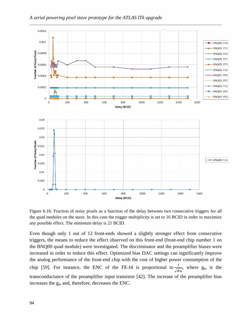
A serial powering pixel stave prototype for the ATLAS ITk upgrade
94
Figure 6.16: Fraction of noisy pixels as a function of the delay between two consecutive triggers for all
the quad modules on the stave. In this case the trigger multiplicity is set to 16 BCID in order to maximize
any possible effect. The minimum delay is 21 BCID.
Even though only 1 out of 12 front-ends showed a slightly stronger effect from consecutive
triggers, the means to reduce the effect observed on this front-end (front-end chip number 1 on
the BNQ00 quad module) were investigated. The discriminator and the preamplifier biases were
increased in order to reduce this effect. Optimized bias DAC settings can significantly improve
the analog performance of the front-end chip with the cost of higher power consumption of the
chip [59]. For instance, the ENC of the FE-I4 is proportional to 1
√𝑔𝑚, where gm is the
transconductance of the preamplifier input transistor [42]. The increase of the preamplifier bias
increases the gm and, therefore, decreases the ENC.

6.3 Characterization of the serially powered detector prototype
95
Figure 6.17 shows a fraction of noisy pixels as a function of the discriminator bias DAC setting
for the 2-trigger noise occupancy scans with a delay of 70 BCID between the two consecutive
triggers performed on the front-end chip number 1 of the BNQ00 quad module. This delay value
is chosen according to the plot on the Figure 6.16, which shows that the effect is the strongest at
this point (peak of the number of noisy pixels). The standard initial tuning configuration is used.
The trigger multiplicity is set to 16. Thus, the discriminator bias is increased starting with the
default value (also used for the IBL), which is indicated on the Figure 6.17. The front-end is
retuned every time the discriminator bias is changed in order to ensure that the threshold setting
is unaltered. As it can be seen from the plot, the increase of the discriminator bias leads to a
significant decrease of the number of noisy pixels as expected. The most optimal discriminator
bias DAC setting for this case is 130. Further increase of the discriminator bias does not lead to
decrease of the number of noisy pixels.
Figure 6.17: Fraction of noisy pixels as a function of the discriminator bias DAC setting for the 2-trigger
noise occupancy scans with a delay of 70 BCID between the two consecutive triggers performed on the
front-end chip number 1 of the BNQ00 quad module. The standard initial tuning configuration is used.
The trigger multiplicity is set to 16. The initial (default) DAC setting of the discriminator bias is shown as
well.
The 2-trigger noise occupancy scans were repeated on the front-end chip number 1 of the
BNQ00 quad module with the most optimal DAC setting of the discriminator bias (130) in order
to ensure that the peak of the number of noisy pixels does not shift to another value of the delay
between the two consecutive triggers. The standard initial tuning configuration is used. The
trigger multiplicity is set to 16. Figure 6.18 shows the result of this investigation. As it can be
seen the peak of the number of noisy pixels does not shift to another value of the delay between
the two consecutive triggers and is significantly reduced.

A serial powering pixel stave prototype for the ATLAS ITk upgrade
96
Figure 6.18: Fraction of noisy pixels as a function of the delay between two consecutive triggers for the
front-end chip number 1 on the BNQ00 quad module. The most optimal DAC setting of the discriminator
bias (130) is used. The trigger multiplicity is set to 16.
The increase of the preamplifier bias reduces the number of noisy pixels as well but not as
significant as the increase of the discriminator bias. Figure 6.19 shows a fraction of noisy pixels
as a function of the preamplifier bias DAC setting for the 2-trigger noise occupancy scans with a
delay of 70 BCID between the two consecutive triggers performed on the front-end chip number
1 of the BNQ00 quad module. The standard initial tuning configuration is used. The trigger
multiplicity is set to 16. Thus, the preamplifier bias is increased starting with the default value
(also used for the IBL), which is indicated on the Figure 6.19. The front-end is retuned every
time the preamplifier bias is changed in order to ensure that the threshold setting is not altered
effectively due to the changed signal amplitude. Unlike the discriminator bias, the preamplifier
bias decreases with the increase of its DAC setting. As it can be seen from the plot, the increase
of the preamplifier bias leads to a decrease of the number of noisy pixels but not as significant as
in case of the discriminator bias increase. The plot also demonstrates that pixels in the outermost
columns of the chip are more sensitive to the digital crosstalk. The increase of the preamplifier
bias for the pixels in the outermost columns allows further reducing the number of noisy pixels
with respect to the case when only the main preamplifier bias is increased proving the fact that a
significant number of the pixels in the outermost columns is affected by the digital crosstalk. The
main preamplifier bias corresponds to all the pixels of the chip apart from the pixels in the
outermost columns.

6.3 Characterization of the serially powered detector prototype
97
Figure 6.19: Fraction of noisy pixels as a function of the preamplifier bias DAC setting for the 2-trigger
noise occupancy scans with a delay of 70 BCID between the two consecutive triggers performed on the
front-end chip number 1 of the BNQ00 quad module. The standard initial tuning configuration is used.
The trigger multiplicity is set to 16. The initial (default) DAC setting of the preamplifier bias is shown as
well. The preamplifier bias decreases with the increase of its DAC setting. Square markers correspond to
the case when only the main preamplifier bias is changed. Diamond shape markers correspond to the case
when the main preamplifier bias and the preamplifier biases for the left and right outermost columns are
changed as well allowing reaching lower values of noisy pixels.
2-trigger noise occupancy scans have as well been performed for the quad modules on the stave
tuned to the baseline threshold. The baseline threshold configuration makes pixels more sensitive
to the digital crosstalk. At first, the trigger multiplicity of 1 is used. Figure 6.20 shows the results
of the scans for the most of the front-ends, which do not show any effect.

A serial powering pixel stave prototype for the ATLAS ITk upgrade
98
Figure 6.20: Fraction of noisy pixels as a function of the delay between two consecutive triggers for most
of the front-ends on the stave. In this case the trigger multiplicity is set to 1 BCID. The minimum delay is
6 BCID. Baseline threshold tuning configuration is used.
However, front-end number 2 of the BNQ01 quad module and front-end number 1 of the BNQ00
quad module show an increase in the number of noisy pixels. For the front-end number 2 of the
BNQ01 quad module the increase in the number of noisy pixels is not significant and can be seen
only for variable delay values below 100 BCID (Figure 6.21). Noisy pixels appear only in the
right outermost column, which in this case is more sensitive to the digital crosstalk (Figure 6.22).
For the front-end number 1 of the BNQ00 quad module the effect is significant leading to all the
pixels on the chip being noisy for a few values of the variable delay (Figure 6.23). As has been
mentioned earlier, this effect is most likely due to the bad decoupling connection of the filtering
capacitor on the module flex and is independent from the powering scheme.

6.3 Characterization of the serially powered detector prototype
99
Figure 6.21: Fraction of noisy pixels as a function of the delay between two consecutive triggers for the
front-end number 2 of the BNQ01 quad module. In this case the trigger multiplicity is set to 1 BCID. The
minimum delay is 6 BCID. Baseline threshold tuning configuration is used.
Figure 6.22: Noisy pixels on the front-end number 2 of the BNQ01 quad module after the standard noise
occupancy scan and after the 2-trigger noise occupancy scan with a delay of 65 BCID between the two
consecutive triggers (peak of the number of noisy pixels)

A serial powering pixel stave prototype for the ATLAS ITk upgrade
100
Figure 6.23: Fraction of noisy pixels as a function of the delay between two consecutive triggers for the
front-end number 1 of the BNQ00 quad module. In this case the trigger multiplicity is set to 1 BCID. The
minimum delay is 6 BCID. Baseline threshold tuning configuration is used.
As expected, a stronger effect is observed when the trigger multiplicity is increased to 16. For the
most of the front-ends the fraction of noisy pixels is higher for the higher trigger multiplicity but
only for the variable delay values below 100 BCID (Figure 6.24). As mentioned, the trigger
multiplicity used for the ATLAS standard operation is 1. A trigger multiplicity of 16 is not
foreseen to be used at the experiment. Front-end number 2 of the BNQ01 quad module and front-
end number 1 of the BNQ00 quad module show a significant increase in the number of noisy
pixels. As indicated earlier, for the front-end number 1 of the BNQ00 quad module this can be
caused by the bad decoupling connection of the filtering capacitor on the module flex
independent from the powering scheme.

6.3 Characterization of the serially powered detector prototype
101
Figure 6.24: Fraction of noisy pixels as a function of the delay between two consecutive triggers for all
the quad modules on the stave. In this case the trigger multiplicity is set to 16 BCID in order to maximize
any possible effect. The minimum delay is 21 BCID. Baseline threshold tuning configuration is used.
6.3.4 Performance studies with noisy modules
As shown in section 6.3.2, the performance of the modules in the chain is not affected if a
number of chips has a noise occupancy higher than 10-5
for a few percent of pixels. To
investigate further the effects of noise propagation in the serial powering chain, a test has been
performed where the global threshold of all four front-end chips on a module is decreased,
making the module noisy. This translates in a higher digital activity, and thus in a higher digital
current than provided (0.15A per chip for the digital power). As shown in [54] and [56], the input

A serial powering pixel stave prototype for the ATLAS ITk upgrade
102
and output voltages of the shunt-LDO regulator collapse if the current flowing in the shunt
transistor is lower than 5 mA, thus switching off the module. As a consequence, the module
current consumption decreases, the voltages across the module can rise again, until the module is
fully on. At this point, the digital activity is high, the current consumption increases and the
voltages collapse, so that an oscillation of the module voltage and current consumption is
induced. Figure 6.25 shows an example of the oscillation on the power line when two modules
are operated with a threshold below the baseline. The amplitude of the oscillation is 380 mV at a
frequency of 120 Hz.
Figure 6.25: Oscillation across the power line with two modules in the chain (i.e. 8 readout chips)
operated with a threshold below the baseline. The amplitude of the oscillation is 380 mV (500 mV/div) at
a frequency of 120 Hz (4 ms/div).
Two different tuning configurations have been used for the quad modules on the stave during the
performance studies with noisy modules: standard tuning and baseline tuning. The following
algorithm has been used to evaluate the performance of the quad modules in the chain while one
or more quad modules in the chain are oscillating:
Performing digital, analog, threshold and noise occupancy scans for reference
Making one (or more) module(s) noisy by lowering the threshold
Number of noise hits increases digital activity increases more current is needed
than supplied voltage across the module oscillates

6.3 Characterization of the serially powered detector prototype
103
Performing digital, analog, threshold and noise occupancy scans with one (or more)
module(s) in the chain being noisy
Bringing module’s threshold back to tuned value
Performing digital, analog, threshold and noise occupancy scans for reference
Only noise occupancy scans have been performed when baseline tuning configuration has been
used due to the fact that the on-chip injection circuit cannot be used in this case.
Threshold scans on the non-oscillating modules tuned with a standard tuning configuration do
not show any performance degradation when one or more modules on the stave are oscillating.
No effect on the threshold and threshold dispersion values has been observed. Tables 6.2 and 6.3
show the ENC and ENC dispersion values for 3 modules, as an example, for the case when there
are no noisy modules in the chain and for the case when one of the modules on the stave is
oscillating. The ENC increased by a maximum of 6 e-, which is well below the ENC dispersion
(≤ 14 e-).
Without noisy Quad
Quad FE read out Noise [e-] Noise dispersion [e-]
BNQ00 FE1 FE4
130 118
12 12
BNQ01 FE2 FE3
155 165
13 14
BNQ05 FE2 FE3
142 148
12 13
Table 6.2: The ENC and ENC dispersion values, obtained with the threshold scans, for 3 modules (as an
example) tuned with a standard tuning configuration for the case when there are no noisy modules in the
chain

A serial powering pixel stave prototype for the ATLAS ITk upgrade
104
Noisy Quad
Quad FE read out Noise [e-] Noise dispersion [e-]
Increase in noise [e-]
BNQ00 BNQ01 FE2 FE3
161 169
13 14
5 4
BNQ05 FE2 FE3
144 151
12 13
2 2
BNQ01 BNQ00 FE1 FE4
136 121
13 12
6 3
BNQ05 FE2 FE3
143 150
12 12
1 2
BNQ05 BNQ00 FE1 FE4
132 119
12 11
2 1
BNQ01 FE2 FE3
157 166
13 14
2 1
Table 6.3: The ENC and ENC dispersion values, obtained with the threshold scans, for 3 modules (as an
example) tuned with a standard tuning configuration for the case when one of the modules on the stave is
oscillating
Analog, digital and noise occupancy scans on the non-oscillating modules tuned with a standard
tuning configuration do not show any performance degradation as well and are identical to the
reference scans.
Noise propagation in the chain has also been tested with modules configured with baseline
threshold. A noise occupancy scan has been performed on the non-oscillating modules for the
case when the voltage across 1 module in the chain was oscillating as well as for the case when
the voltage across 2 modules in the chain was oscillating (Figure 6.25). No increase of the noise
occupancy has been observed.
These results are in agreement with what was observed in [51] and [53], and thus confirm that a
disturbance on the power line is not a concern in a serially powered pixel system.
6.3.5 Performance studies with bypassed modules
Prior to the performance studies with bypassed modules the communication with the PSPP chip
when the serial current for the modules is off has been tested. This test had to be performed due
to the fact that this may be the case during the power up of the pixel detector where the power
line for the PSPP chip and the serial current will share the same ground as in the current setup.

6.3 Characterization of the serially powered detector prototype
105
The tests have shown that the communication is not affected when the serial current for the
modules is off.
The details of the verification of the autonomous fault detection feature of the PSPP chip,
performed on a standalone module, can be found in [49].
Performance studies with statically and dynamically bypassed modules have been made in order
to prove that bypassing of one or more modules does not influence the performance of other
modules in the serial powering chain. Static bypassing in this case means that the scans were
performed on the non-bypassed modules after some of the other modules in the chain were
bypassed. Dynamic bypassing in this case means that that some of the modules on the stave were
bypassed during the time when the scans were running on the non-bypassed modules. Two
different tuning configurations have been used for the quad modules on the stave during the
performance studies with bypassed modules: standard tuning and baseline tuning. The following
algorithm has been used to evaluate the performance of the quad modules in the chain while one
or more quad modules in the chain are bypassed:
Performing digital, analog, threshold and noise occupancy scans for reference
Bypassing one (or more) module(s) with the shunting command to the PSPP chip
Performing digital, analog, threshold and noise occupancy scans with one (or more)
module(s) in the chain being bypassed
Turning bypassed module(s) back on
Performing digital, analog, threshold and noise occupancy scans for reference
Only noise occupancy scans have been performed when baseline tuning configuration has been
used due to the fact that the on-chip injection circuit cannot be used in this case.
Figure 6.26 shows the voltage across the chain when activating the PSPP chip on one module.
The voltage decrease indicates that the module is successfully powered off. A residual voltage of
approximately 300 mV is left across the shunt transistor in the PSPP chip. The time to switch off
the chip is about 5 ms. This is dominated by the time response of the current source and the cable
electrical properties, and it is thus specific to this setup and not to the chip.

A serial powering pixel stave prototype for the ATLAS ITk upgrade
106
Figure 6.26: Voltage drop across the serial powering chain observed during the bypass activation. The
voltage across the chain is 13.6 V (2 V/div) when all the modules are powered. The voltage is reduced to
11.9 V in about 5 ms (1 ms/div) when one module is bypassed.
Figure 6.27a shows a schematic diagram of the quad modules on the stave. Some of the quad
modules have on-flex PSPP chip which allows bypassing a certain module. Services for the
PSPP chips are provided in parallel via a PSPP master board (Section 6.1). All bypass transistors
are open during the standard operation of the stave and therefore all the modules are powered.
With this configuration reference scans have been made. Figure 6.27b shows the case after two
of the quad modules have been bypassed and the other quad modules observe voltage drop from
the bypass activation.

6.3 Characterization of the serially powered detector prototype
107
Figure 6.27: (a) Schematic diagram of the quad modules on the stave with the PSPP chips and
corresponding services for the standard operation case when all the bypass transistors are open. (b) The
case after two of the quad modules have been bypassed and the other quad modules observe voltage drop
from the bypass activation.
The performance studies with the dynamically bypassed modules have been made in order to
check whether the non-bypassed modules are affected and to find out how strong is this effect. It
was also necessary to prove that the dynamic effect from the bypass happens only during the
switching of the PSPP chip and does not extend beyond this time. The switching time of the
PSPP chip has been measured and is about 5 ms (Figure 6.26). Standard tuning configuration has
been used for the modules during the dynamic bypassing tests.
No effect from the dynamic bypass activation has been observed in threshold scans. However a
small effect can be seen in noise occupancy scans on some of the non-bypassed modules (Figure
6.28b). 107 triggers have been sent during the noise occupancy scan. Analysis of the hit data has
shown that there were no more than 3 hits per pixel. Moreover, the recorded hits appeared
approximately during the time when the bypasses were activated. Therefore, it can be concluded
that the dynamic effect from the bypass is short, small and happens only during switching.

A serial powering pixel stave prototype for the ATLAS ITk upgrade
108
Figure 6.28: (a) Reference noise occupancy scan results for the two front-ends. (b) Effect on the front-
ends from the dynamic bypass activation.
The most important for the detector operation is that the correct functioning of the non-bypassed
modules is re-established after the bypass activation on one or more modules is finished. This
has been proven with performance studies with statically bypassed modules.
Threshold scans on the non-bypassed modules tuned with a standard tuning configuration do not
show any performance degradation, when 1, 2 or 3 quad modules on the stave are bypassed
statically. No effect on the threshold and threshold dispersion values has been observed. Tables
6.4 and 6.5 show the ENC and ENC dispersion values for all quad modules on the stave for the
case when there are no bypassed modules in the chain and for the case when 3 quad modules on
the stave are bypassed statically. No effect on the ENC and ENC dispersion values has been
observed as well.

6.3 Characterization of the serially powered detector prototype
109
Without bypassed
Quads
Quad FE read out Noise [e-] Noise dispersion [e-]
BNQ00 FE1
FE4
131
118
12
12
BNQ01 FE2
FE3
154
162
13
14
BNQ05 FE2
FE3
141
148
12
13
BNQ02 FE3
FE4
138
154
12
14
BNQ03 FE2
FE3
141
137
13
12
BNQ04 FE4
FE3
144
159
13
14
Table 6.4: The ENC and ENC dispersion values, obtained with the threshold scans, for all quad modules
on the stave tuned with a standard tuning configuration for the case when there are no bypassed modules
in the chain
BNQ02, BNQ03, BNQ04
bypassed
Quad FE read out Noise [e-] Noise dispersion [e-]
BNQ00 FE1
FE4
130
117
12
12
BNQ01 FE2
FE3
154
164
13
14
BNQ05 FE2
FE3
141
148
12
12
Table 6.5: The ENC and ENC dispersion values, obtained with the threshold scans, for all quad modules
on the stave tuned with a standard tuning configuration for the case when 3 quad modules on the stave are
bypassed statically
Analog, digital and noise occupancy scans on the non-bypassed modules tuned with a standard
tuning configuration do not show any performance degradation as well, when 1, 2 or 3 quad
modules on the stave are bypassed statically, and are identical to the reference scans.
Static bypassing effects in the chain have also been investigated with modules configured with
baseline threshold. A noise occupancy scan has been performed on the non-bypassed modules

A serial powering pixel stave prototype for the ATLAS ITk upgrade
110
when 1, 2 or 3 quad modules on the stave have been bypassed statically. No increase of the noise
occupancy has been observed.
Table 6.6 summarizes the tests performed on the non-bypassed modules when 1, 2 or 3 quad
modules on the stave have been bypassed statically. No difference in performance has been
measured.
Tuning configuration Test Results
Standard tuning Analog test
Digital test
Threshold scan
Noise occupancy scan
Performance of the analog and digital
parts of the front-end chip unchanged
Performance of the digital part of the
front-end chip unchanged
No effect on threshold, threshold
dispersion, ENC and ENC dispersion
No increase in noise occupancy
Baseline threshold tuning Noise occupancy scan No increase in noise occupancy
Table 6.6: Summary of the tests performed on the non-bypassed modules when 1, 2 or 3 quad modules on
the stave have been bypassed statically
6.3.6 Crosstalk test
A crosstalk test has been performed for the serially powered pixel detector prototype in order to
prove that clock, command and data channels of different quad modules on the stave do not
affect each other during operation. First of all reference threshold scans were performed
consecutively for every module. Thus the modules were configured and read out one by one.
Afterwards, the threshold scans were performed for all the quad modules on the stave
simultaneously. Thus the configuration of all the modules was performed at the same time and
therefore all the command and clock lines were active. Data from all the modules were readout
simultaneously as well and separated in the software. Table 6.7 shows the comparison of the
threshold, the threshold dispersion and the equivalent noise charge for all the modules on the
stave obtained from the consecutive (reference) threshold scans and the simultaneous (crosstalk)
threshold scans.

6.3 Characterization of the serially powered detector prototype
111
Threshold scan Quad FE read out Threshold [e-] Threshold dispersion [e-] Noise [e-]
Consecutive
BNQ00 FE1
FE4
1472
1532
26
24
132
119
BNQ01 FE2
FE3
1488
1469
29
28
157
164
BNQ05 FE2
FE3
1511
1470
31
31
141
149
BNQ02 FE3
FE4
1536
1548
26
27
138
151
BNQ03 FE2
FE3
1559
1552
29
24
142
139
BNQ04 FE4
FE3
1549
1546
26
25
157
145
Simultaneous
BNQ00 FE1
FE4
1472
1526
25
24
129
120
BNQ01 FE2
FE3
1482
1468
30
28
155
163
BNQ05 FE2
FE3
1511
1473
30
31
140
149
BNQ02 FE3
FE4
1538
1548
26
28
137
151
BNQ03 FE2
FE3
1556
1554
30
24
142
138
BNQ04 FE4
FE3
1551
1545
27
25
158
145
Table 6.7: Comparison of the threshold, threshold dispersion and the equivalent noise charge for all the
modules on the stave obtained from the consecutive (reference) threshold scans and the simultaneous
(crosstalk) threshold scans
No significant effect can be observed on the threshold, threshold dispersion and the equivalent
noise charge for the simultaneous (crosstalk) threshold scans with respect to the reference
threshold scans and therefore the results confirm that clock, command and data channels of
different quad modules on the stave do not affect each other during operation.
6.3.7 Source scan

A serial powering pixel stave prototype for the ATLAS ITk upgrade
112
A source scan is performed as a final test for all the quad modules on the stave. This scan records
hits from a radioactive source and allows mimicking the operation of the pixel detector in the
experiment. It also validates the performance of the modules from charge collection in the sensor
to hit processing in the front-end chip and data outputting. For this test an 241
Am source was
used. The source has been placed at different locations to readout hits from the modules on both
sides of the stave (Figure 6.29). A fraction of low energy gamma rays emitted by the 241
Am
source is absorbed by atomic electrons that are hence moved into the conduction band due to the
photoelectric effect that is the dominant process at low photon energies, in silicon below about
100 keV as shown on the Figure 3.2 in the Section 3.5 [13]. The self-trigger mode, described in
detail in Section 4.6.1, of the FE-I4 readout chip has been used for the source scan. Thus the
trigger signal in this case is generated by the front-end every time a hit is recorded. The noise
occupancy and stuck pixel tunings have been performed prior to the source scan in order to mask
noisy and stuck pixels. Noisy pixels have to be removed due to the fact that they affect the
recorded hit map and ToT distribution. Stuck pixels keep the HitOR signal constantly active high
and thus have to be removed in order to enable self-triggering mode.
Figure 6.29: Serially powered pixel stave prototype and an 241
Am source, which can be moved along the
stave with the help of a dedicated support structure
Figure 6.30 shows a schematic representation of the modules on the stave, where the hit maps
obtained from the source scan are shown on the corresponding front-end chips. Hits are recorded
in all pixels illuminated by the source. The dotted lines represent modules on the bottom side of
the stave. The position of the source for the various scans is shown as well. A higher number of
hits is recorded in correspondence to the source location. Areas of lower hit counts can be seen
below the passive components on the module flex, and below the weights used to hold the
modules in contact with the stave. The latter can be seen as large dark blue regions in the plot. A
lower number of hits is obtained also on the modules on the bottom side of the stave. Here a
more homogenous distribution of hits is observed. As the gamma rays illuminate the sensor from
the back side, there is no interaction with the components on the module flex.

6.3 Characterization of the serially powered detector prototype
113
Figure 6.30: A schematic representation of the modules on the stave, where the hit maps obtained from
the source scan are shown on the corresponding front-end chip. The position of the source for the various
scans is shown as well.
The ToT distribution for the front-end number 3 on the BNQ01 quad module as an example is
shown on the Figure 6.31. The peak in the distribution corresponds to a charge of ~16 ke-. The
charge resolution of the FE-I4 readout chip is limited by the 4 available bits for the ToT code.
The error on the calibration of the injected charge is about 5 %. The charge of ~16 ke-
corresponds to an energy of ~57.6 keV which is in a very good agreement with the 60 keV peak
of the 241
Am source spectrum. This result is in agreement with the one obtained for the single
FE-I4 chip powered with constant voltage, presented in Section 4.6.1.
Figure 6.31: The ToT distribution for the front-end number 3 on the BNQ01 quad module as an example
The results of the source scan prove that all features of the serial powering chain, from voltage
generation, to data transmission and sensor biasing work correctly, and demonstrate that a

A serial powering pixel stave prototype for the ATLAS ITk upgrade
114
serially powered pixel detector can operate error free for up to 10 hours in the conditions
corresponding to later operation in the experiment.

115
Chapter 7
Conclusion and Outlook
The LHC upgrade to the HL-LHC is foreseen in the near future in order to increase the
probability of new discoveries. This includes the upgrade of the ATLAS detector.
During the LHC Long Shutdown 3 (LS3) and the full luminosity LHC upgrade (HL-LHC) which
is foreseen around 2025 the entire ATLAS tracking system will be replaced by an all-silicon
detector called Inner Tracker (ITk) which should be able to withstand the increased luminosity of
5×1034
cm-2
s-1
. The ITk is foreseen to include 4 strip barrel layers supplemented with 2×6 end-
cap disks and 5 pixel barrel layers. The work presented in this thesis is focused on the ATLAS
ITk pixel detector upgrade.
Advanced silicon pixel detectors will be an essential part of the ITk pixel detector where they
will be used for tracking and vertexing. Characterization of the pixel detectors is one of the
required tasks for a successful ATLAS Tracker upgrade. Therefore a versatile and modular test
system for advanced silicon pixel detectors for the HL-LHC has been developed in the
framework of this thesis. This includes hardware, firmware and software developments. The
developed system is called USBpix3 and it can be used for readout and characterization of
single- and multi-chip pixel modules as well as multiple pixel modules (i.e. FE-I4 based quad
modules). The readout and characterization of next generation front-ends that are currently being
developed for the ATLAS ITk pixel detector can also be performed with the USBpix3 readout
system. Dedicated tests have been made in order to verify the performance of the developed USB
3.0 microcontroller and FPGA firmware as well as the developed hardware. All the performed
tests proved an excellent performance of the readout system. It has been shown that the readout
system can cope with data rates of up to 2.24 Gbit/sec (1 Gbit/sec) while maintaining the data
integrity when the USB 3.0 interface (Ethernet interface) is used to connect to the data
acquisition PC. The multi-gigabit transceivers and the clocking resources of the readout system
have shown error-free operation at a line rate of 3.125 Gbit/sec and, therefore, can be reliably
used for the readout and characterization of the RD53 readout chips, that are currently being
developed. The developed USBpix3 readout system has been used to characterize single and
quad FE-I4 modules functionalities. The results of the measurements confirmed the correct
operation of the USBpix3 and verified that the tested single and quad FE-I4 modules function
correctly. Single FE-I4 module was powered according to the standard voltage-based powering
scheme, while quad FE-I4 modules were powered according to the serial powering scheme.
Analog and digital parts of the tested single FE-I4 module show less than 0.02 % of failing

Conclusion and Outlook
116
pixels. The hit detection threshold can be tuned precisely to the target value of 1500 e-, and the
threshold dispersion across the pixel matrix is only ~ 30 e- after tuning. The feedback current is
successfully tuned in such a way that a return to baseline within 250 ns (10 ToT) is obtained for
a signal corresponding to 16 ke-. The equivalent noise charge (ENC) is characterized as well.
The ENC after the tuning is about 130 e-. Expected results have been obtained as well with a
source scan performed with an 241
Am source. All the obtained results are in a very good
agreement with the results of the same measurements performed with the USBpix readout
system. The results obtained during characterization of standalone quad FE-I4 modules, powered
according to the serial powering scheme, are in agreement with the results of the single FE-I4
module characterization: less than 0.04 % of failing pixels are registered in the analog and digital
parts of every front-end; target threshold of 1500 e- is reached with dispersion below 30 e
-, target
ToT is reached as well; the ENC after the tuning is between 120 and 160 e-. The results obtained
with single and quad FE-I4 modules prove that the USBpix3 readout system can be reliably used
for the readout of single and multiple front-ends. These results were also used as one of the
references for the measurement results of the serially powered pixel detector prototype. Up to
now about 80 units of the USBpix3 readout system have been produced, tested and distributed to
many groups in ATLAS, CMS, Belle II and other collaborations. These numbers are expected to
grow in the future. Broad functionality available for the characterization of advanced silicon
pixel detectors along with high bandwidth, light weight and small size make the USBpix3
readout system highly popular in the LHC collaboration and beyond.
One of the main challenges for the ATLAS ITk Phase II Pixel upgrade is a low mass, efficient
power distribution to power detector modules. This requires a powering scheme alternative to the
parallel (direct) powering which is currently used. A serial powering scheme reduces power
losses in the cables, cable material, total detector power consumption and number of power
supply channels and therefore increases power efficiency and reduces material budget and costs.
In the framework of this thesis a serially powered pixel detector prototype has been built with all
the components that are needed for current distribution, data transmission, sensor biasing,
bypassing and redundancy in order to demonstrate the operation of modules powered in series by
servicing a constant current, instead of providing a voltage to each module independently or in
parallel as traditionally done in high energy physics experiments. Detailed investigations of the
electrical performance of the serially powered stave, equipped with FE-I4 quad modules,
including threshold homogeneity, noise occupancy, robustness against noise, crosstalk and
power failures, operation with low detection threshold and consecutive trigger commands have
been made. Performance studies with radioactive source have been made in order to confirm that
the modules work properly, from charge collection in the sensor to hit processing in the front-end
and data outputting. A bypass scheme based on the PSPP chip has also been validated as a
further safety measure in case of failure of modules in the chain. The modules showed excellent
performance both under standard working conditions, as well as in more challenging operating
scenarios. Less than 0.04 % of failing pixels are registered in the analog and digital parts of every
front-end. The target threshold is reached on all the modules in the chain with dispersion below

6.3 Characterization of the serially powered detector prototype
117
30 e-. The target ToT is reached as well. The ENC after the tuning is between 120 and 160 e
-.
The number of modules in the chain does not influence threshold dispersion and noise values. A
stable minimum threshold between 600 and 800 e- can be reached with the help of the novel
baseline threshold tuning algorithm. Consecutive triggers do not affect the modules in the chain
stronger than in the parallel powering scheme. Noisy and bypassed modules do not affect the rest
of the modules in the chain significantly. The correct operation of the bypass scheme is
confirmed. No crosstalk between the modules is observed. Expected results are obtained as well
with a source scan performed with an 241
Am source. All the obtained results are in a very good
agreement with respect to the voltage based powering scheme. The USBpix3 readout system has
been used for the stave readout and proved to be suitable for the parallel readout of multiple FE-
I4 quad modules. The work presented in the thesis confirmed the feasibility of implementing the
serial powering scheme in the ITk. The serial powering scheme has been chosen as the baseline
for the ATLAS ITk pixel system.
Improvements in the regulator design as well as in the bypass, AC-coupling and high voltage
distribution schemes would allow reaching even higher power efficiency and lower mass for the
serial powering. Further investigations for the serial powering scheme have to be performed as
well with the pixel detector prototypes closer to the final ITk pixel detector design. In this case
the detector modules have to be based on the next generation front-ends (RD53 readout chips)
that are currently being developed. The built detector prototype can become a reference for the
next designs. The developed measurement concepts as well as the results obtained in the
framework of this thesis can serve as a basis for the future tests. The developed USBpix3 readout
system can be used for the future investigations as it has been proven that the USBpix3 can
support the readout and characterization of the next generation front-ends.

Bibliography
118
Bibliography
[1] G. Aad et al. Observation of a new particle in the search for the Standard Model Higgs
boson with the ATLAS detector at the LHC. Phys. Lett., B716: 1–29, 2012.
[2] CERN. New results indicate that particle discovered at CERN is a Higgs boson. CERN
press release, March 2013.
[3] L. Evans and P. Bryant. LHC Machine. JINST, 3:S08001, 2008.
[4] The ATLAS Experiment home page, http://www.atlas.ch.
[5] ATLAS Collaboration. The ATLAS Experiment at the CERN Large Hadron Collider.
JINST, 3:S08003, 2008.
[6] ATLAS Collaboration. ATLAS detector and physics performance: Technical Design
Report, 1. Tech. rep. Geneva: CERN, 1999.
[7] ATLAS Collaboration. The ATLAS experiment at CERN.
http://www.atlas.ch/photos/full-detector-cgi.html.
[8] ATLAS Collaboration. ATLAS pixel detector electronics and sensors. JINST, 3:P07007,
2008.
[9] A new subdetector for ATLAS, https://home.cern/about/updates/2014/05/new-
subdetector-atlas
[10] ATLAS Collaboration. Letter of Intent for the Phase-II Upgrade of the ATLAS
Experiment. Technical Report CERN-2012-022. LHCC-I-023, CERN, Geneva,
December 2012.
[11] A. Kluge, G. Aglieri Rinella, G. Anelli et al. The ALICE silicon pixel detector. Nucl.
Instrum. Meth., A582: 728–732, 2007.
[12] H.C. Kaestli, W. Bertl, W. Erdmann et al. CMS barrel pixel detector overview. Nucl.
Instrum. Meth., A582: 724–727, 2007.
[13] P. Rossi L. Fischer, T. Rohe and N. Wermes. Pixel detectors: From fundamentals to
applications. Springer, 2006.
[14] N. Wermes. Pixel vertex detectors. 2006.

119
[15] RD53 Collaboration, http://rd53.web.cern.ch/RD53/
[16] M. Garcia-Sciveres et al., Towards third generation pixel readout chips. Nucl. Instrum.
Meth., A731: 83-87, 2013.
[17] J. Weingarten, S. Altenheiner, M. Beimforde, M. Benoit, M. Bomben, et al. Planar Pixel
Sensors for the ATLAS Upgrade: Beam Tests results. JINST, 7:P10028, 2012.
[18] C. Gallrapp. Planar Pixel Sensors for the ATLAS tracker upgrade at HL-LHC. Nucl.
Instrum. Meth., A718: 323–324, 2013.
[19] C. Da Via et al. 3D silicon sensors: Design, large area production and quality assurance
for the ATLAS IBL pixel detector upgrade. Nucl. Instrum. Meth., A694: 321–330,
December 2012.
[20] I. Peric. A novel monolithic pixelated particle detector implemented in high voltage
CMOS technology. Nucl. Instrum. Meth., A582: 876–885, 2007.
[21] W. Snoeys. Monolithic pixel detectors for high energy physics. Nucl. Instrum. Meth.,
A731: 125–130, 2013.
[22] N. Savic et al. Thin n-in-p planar pixel modules for the ATLAS upgrade at HL-LHC.
ArXiv:1605.00463, 2016.
[23] M. Garcia-Sciveres, D. Arutinov, M. Barbero et al. The FE-I4 pixel readout integrated
circuit. Nucl. Instrum. Meth., A636: S155–S159, 2011.
[24] M. Barbero et al. The FE-I4 Pixel Readout Chip and the IBL Module. Proceedings of
Science, PoS, Vertex, 2011
[25] FE-I4 Collaboration. The FE-I4B Integrated Circuit Guide. Version 2.3, December 30,
2012
[26] D. Arutinov et al. Digital architecture and interface of the new ATLAS Pixel Front-End
IC for upgraded LHC luminosity. IEEE Transactions on Nuclear Science 56(2), April
2009
[27] ATLAS Collaboration. Phase-II Upgrade Scoping Document. Technical Report CERN-
2015-020. LHCC-G-166, CERN, Geneva, September 2015.
[28] Enclustra official web site, http://www.enclustra.com/en/products/fpga-
modules/mercury-kx1/
[29] Cypress official web site, http://www.cypress.com/products/ez-usb-fx3-superspeed-usb-
30-peripheral-controller

Bibliography
120
[30] PyBAR development web page, https://github.com/SiLab-Bonn/pyBAR
[31] Basil development web page, https://github.com/SiLab-Bonn/basil
[32] J. Janssen, Development of an FPGA-based FE-I3 pixel readout system and
characterization of novel 3D and planar pixel detectors, Diploma thesis BONN-IB-2010-
08 (2010).
[33] USBpix readout system web page, http://icwiki.physik.uni-
bonn.de/twiki/bin/view/Systems/UsbPix
[34] T. Flick et al. The Phase II ATLAS Pixel Upgrade: The Inner Tracker (ITk) - ATL-ITK-
PROC-2016-006.
[35] N. Savic et al., Investigation of thin n-in-p planar pixel modules for the ATLAS
upgrade, Proceedings of the 18th IWORID workshop, submitted to JINST (2016).
[36] J. Lange et al., 3D silicon pixel detectors for the High-Luminosity LHC, Proceedings of
the 8th
International Workshop on Semiconductor Pixel Detectors for Particles and
Imaging, to be published in JINST. September, 2016. arXiv:1610.07480v2
[37] M. Garcia-Sciveres and J. Christiansen, RD Collaboration Proposal: Development of
pixel readout integrated circuits for extreme rate and radiation, CERN-LHCC-2013-008
(2013), URL:http://cds.cern.ch/record/1553467
[38] T. Heim et al., FE65-P2: a Prototype Pixel Readout Chip in 65 nm Technology for HL-
LHC Upgrades, to be submitted to 2016 IEEE Nuclear Science Symposium Conference
Record (2016).
[39] H. Correia et al., ATLAS Large eta task force report, CERN, ATL-UPGRADE-INT-
2015-001, (2015).
[40] A. J. Barr et al., Higgs Self-Coupling Measurements at a 100 TeV Hadron Collider,
JHEP 02 (2015) 016, 1412.7154.
[41] S. McMahon et al., High Level Functional Requirements of the ITk: High Level
Functional Requirements of the ITk, CERN, ATL-COM-UPGRADE-2015-015, (2015).
[42] J.-W. Tsung et al., Signal and noise of Diamond Pixel Detectors at High Radiation
Fluences, JINST 7 (2012), 10.1088/1748-0221/7/09/P09009.

121
[43] M.-A. Karagounis. Analog Integrated CMOS Circuits for the Readout and Powering of
Highly Segmented Detectors in Particle Physics Applications, PhD thesis,
FernUniversität Hagen.
[44] M. Havránek et al., Measurement of pixel sensor capacitances with sub-femtofarad
precision, Nucl. Instrum. Meth., A, 2013.
[45] IBERT for 7 Series GTX Transceivers Xilinx web page,
https://www.xilinx.com/products/intellectual-property/ibert_7series_gtx.html
[46] Understanding and Characterizing Timing Jitter, Tektronix Primer, 2003.
[47] M. Backhaus, The upgraded Pixel Detector of the ATLAS Experiment for Run 2 at the
Large Hadron Collider, Nucl. Instrum. Meth. A, 2016, http://dx.doi.org/10.1016/j.
nima.2016.05.018i
[48] V. Filimonov et al., A serial powering pixel stave prototype for the ATLAS ITk
upgrade, JINST (2017), 10.1088/1748-0221/12/03/C03045.
[49] L. Gonella et al., Performance evaluation of a serially powered pixel detector prototype
for the HL-LHC, JINST (2017), 10.1088/1748-0221/12/03/P03004.
[50] M. Weber. Power distribution for SLHC trackers: Challenges and solutions. Nucl.
Instrum. Meth. A592: 44–55, 2008.
[51] D.B. Ta, T. Stockmanns, F. Hugging, P. Fischer, J. Grosse-Knetter, O. Runolfsson et al.,
Serial powering: Proof of principle demonstration of a scheme for the operation of a large
pixel detector at the LHC, Nucl. Instrum. Meth. A 557, 2006.
[52] ATLAS collaboration, Progress and advances in serial powering of silicon modules for
the ATLAS tracker upgrade, 2011 JINST 6 C01019.
[53] L. Gonella, Low mass hybrid pixel detectors for the high luminosity LHC upgrade, PhD
thesis, BONN-IR-2013-18 (2013).
[54] M. Karagounis et al., An integrated Shunt-LDO regulator for serial powered systems, in
Proceedings of ESSCIRC, Athens, 2009, pp. 276–279.
[55] L. Puellen, Development of a Detector Control System for the serially powered ATLAS
pixel detector at the HL-LHC, PhD thesis, Bergische Universität Wuppertal (2015).

Bibliography
122
[56] L. Gonella et al., The shunt-LDO regulator to power the upgraded ATLAS pixel
detector, 2012 JINST 7 C01034
[57] National Semiconductor, LVDS Owner’s Manual,
http://www.ti.com/lit/ml/snla187/snla187.pdf
[58] RD53 Collaboration, RD53A Integrated Circuit Specifications, Version 3.2, Dec. 13,
2015
[59] J. Janssen, Test beam results of ATLAS DBM pCVD diamond detectors using a novel
threshold tuning method, accepted for publication in JINST (2016).
[60] The ATLAS collaboration, ATLAS Pixel IBL: Stave Quality Assurance, ATLAS
NOTE, ATL-INDET-PUB-2014-006, September 10, 2014
[61] STEP1 ITk Layout Studies,
https://atlas.web.cern.ch/Atlas/GROUPS/PHYSICS/PLOTS/ITK-2016-001/
[62] USBpix3 distribution tables, http://icwiki.physik.uni-
bonn.de/twiki/bin/view/Systems/USBpix3Tables
[63] C. Grupen, Particle detectors, 2008
[64] R. L. Gluckstern, Uncertainties in track momentum and direction, due to multiple
scattering and measurement errors, Nucl. Instrum. Meth. 24 (1963), pp. 381–389
[65] F. Ragusa and L. Rolandi, Tracking at LHC, New J. Phys. 9 (2007), p. 336
[66] J. Grosse-Knetter, Vertex Measurement at a Hadron Collider - The ATLAS Pixel
Detector, BONN-IR-2008-04, PhD thesis, 2008
[67] H. Kolanoski, N. Wermes, Teilchendetektoren: Grundlagen und Anwendungen, 2015
[68] G.R. Lynch, O.I. Dahl. Approximations to multiple Coulomb scattering, Nuclear Instr.
Meth. B 58 (1991), pp. 6–10

123
Appendix
Alternative upgrade options considered for the USBpix
Several upgrade options have been considered in order to overcome the limitations of the
MultiIO board.
The most straightforward option is to fully redesign the MultiIO board and include larger FPGA
and memory, USB 3.0 and Gbit Ethernet interfaces leaving the board downward compatible with
the USBpix adapter cards and software. This option provides the highest flexibility but it also
requires the highest development effort and has the highest risk.
Another option is to use a commercial evaluation board which already has all the necessary
components and interfaces and to design a passive connector adapter to provide compatibility
with the USBpix adapter cards. This option requires the lowest development effort but it also
provides the lowest flexibility and may lead to mechanical issues due to the fact that evaluation
boards include many components that are not needed for the detector readout. These components
increase the form factor of the board significantly.
The selected upgrade option assumes using a commercial FPGA module with a custom made
carrier board (Section 4.2). All the upgrade options are summarized in Table 1.
Upgrade Option Flexibility Development effort Comment
Full redesign of the
MuliIO board High High
Highest development
risk
Commercial
evaluation board
with adapter
Low Low Large form factor
Commercial FPGA
module with custom
carrier board
Medium / High Medium Freedom to design a
custom carrier board
Table 1: USBpix upgrade options

Appendix
124
Firmware, hardware and software of the USBpix3 readout system
A detailed block diagram showing developed firmware, hardware and software for the USBpix3
readout system can be seen on Figure 1. A complete description of every block of the diagram is
given in a dedicated section below.
Figure 1: A detailed block diagram showing developed firmware, hardware and software for the USBpix3
readout system
Firmware of the USBpix3
USB 3.0 microcontroller firmware
In order to implement USB 3.0 functionality in the USBpix3 a dedicated firmware has been
developed for the FX3 device [29] which is a USB 3.0 microcontroller that includes an ARM
CPU. The Enclustra Mercury KX1 FPGA module holds the FX3 device. The existing software
framework of the USBpix readout system (pyBAR [30]) is compatible to the developed firmware
which connects the FPGA module to a data acquisition computer (host).
Implementation of a USB 3.0 interface includes configuration of four endpoints for different
transfer types as well as USB enumeration descriptors in order to send data to the host and
receive data from it. Figure 1 shows the configured endpoints. Endpoints 2 and 6 are used for
block transfers in DMA auto channels that are implemented between USB endpoints and General
Programmable Interface (GPIF) sockets to maximise the transfer speed between the host and the

125
FPGA as these channels operate without CPU intervention. Endpoint 1 is used for control
transfers and slow peripherals such as I2C and SPI interfaces that are configured to allow
accessing EEPROM and SPI Flash on-board. I2C and SPI transfers use DMA manual channels
that are implemented as well and suppose CPU intervention.
Connectivity between the FX3 device and the FPGA is realized with the GPIF interface which is
integrated in the FX3 device (Figure 1) and can be configured by the means of state machine.
The GPIF can function as master or slave. It provides 256 firmware programmable states,
supports 8, 16 and 32-bit parallel data bus, enables interface frequencies up to 100 MHz and
supports 14 configurable control pins when 32 bit data bus is used. All control pins can be either
input/output or bidirectional.
In current application the GPIF is used to control the FPGA. In other words the FX3 is a master
and the FPGA is a slave. Figure 2 shows other electrical details of the GPIF. Both I2C and SPI
interfaces are implemented in the FX3 firmware, however it’s not possible to use the SPI
interface together with 32-bit data bus of the GPIF. Communication type is synchronous, internal
100 MHz clock is used with negative clock edge, data bus is 32 bits wide and is multiplexed with
the address bus. Some control signals are also used. All signals are set to active high.
Figure 2: Electrical details of the General Programmable Interface of the FX3 device
The logic of the GPIF is defined in the form of a state machine diagram as shown on Figure 3.
The state machine consists of two main loops. One loop is responsible for writing to the FPGA

Appendix
126
and another loop is responsible for reading from the FPGA. First of all after application is started
and the GPIF interface is initialized, the state machine goes to RESET state where it drives Reset
output to reset the FPGA. Then depending on the type of the request from the host it switches to
the reading loop of the state machine or to the writing loop of the state machine. The first state in
writing loop is IDLE_WRITE. It will go to the Drive Address state (WR_DR_ADDR) if the data
in the corresponding DMA socket is available. If this is the case it goes first to the
WR_WAIT_REGS state in order to wait for the address register to be filled and afterwards it
goes to the WR_DR_ADDR state (if the data in the address register is valid), drives the address
to the data bus and signals the FPGA about the started transfer. Several delay states in the state
machine such as WR_ADDR_DELAY, which the state machine enters next, are necessary to
synchronize the timing between the FX3 and the FPGA and in this case to account for the time
that is needed for the address to be driven to the data bus. Then the state machine goes to the
Drive Count state (WR_DR_COUNT) which is needed to drive the counter value to the data bus.
This value is used by the FPGA for counting the incoming data. Another delay after that
(WR_COUNT_DELAY) is used for the reason explained above. When the FPGA receives the
address and the counter value it answers with RDY signal and the state machine can go to the
WR_DATA state which is used for driving data to the data bus. An additional output signal is
used here to notify the FPGA that the data is present on the data bus. The data is driven to the
data bus only until the data in the corresponding DMA socket is available and the FPGA is ready
to accept the data. If the FPGA is not ready to accept the data the state machine goes to the
WR_WAIT state where it waits until the FPGA is ready. After the data transfer the state machine
returns to the IDLE_WRITE state. Reading loop works in a similar manner. As it has been
already mentioned the data transfer with the GPIF interface is done with the help of DMA
Factory without CPU intervention.

127
Figure 3: State machine diagram of the General Programmable Interface of the FX3 device
GPIF and FPGA timing parameters are taken into account during the firmware development.
Dedicated simulations with FX3 development software (GPIF II Designer) and with FPGA
development software (ISim) have been performed in order to verify the correct operation of the
interface.
FPGA firmware
The implemented Kintex-7 FPGA firmware provides the connectivity to the FX3 device, to the
USBpix adapter cards (in case of the MIO3 board) and a number of peripheral connectors and
interfaces that are described in detail in the next section. It also provides readout and
configuration logic for pixel readout chips and modules which is the main goal of the USBpix3
readout system. The FPGA firmware is organized in a modular structure where every module has
its address space (Figure 1).
An FX3 interface module is implemented for data transfer between the FPGA logic and the FX3
device. A finite state machine (FSM) is a core of this module. It interacts with the state machine
of the GPIF interface (Figure 3) during the data transfer and thus is implemented in a similar
manner. This module also provides a buffer for the 100 MHz design clock that comes from the
FX3, 32 bit to 8 bit and vice versa data bus adapter in case 8-bit data bus has to be used

Appendix
128
internally in the FPGA (this is the case for older versions of the FPGA modules) and a tristate
buffer for the data bus between the FX3 and the FPGA.
A command sequencer module is dedicated for providing clock and command signals for the
front-end. Several command output modes are available: command synchronized with the
positive edge of the clock / negative edge of the clock, Manchester encoded command according
to IEEE 802.3 standard and Manchester encoded command according to G.E. Thomas standard
(also known as Biphase-L code or Manchester-II code). Manchester encoded command
according to IEEE 802.3 standard is used in the firmware for the MMC3 board to realize AC-
coupled data transmission which is needed for the Serially Powered Stave readout where each
module has different ground potential. Differential drivers for clock and command lines are
implemented in the MMC3 FPGA firmware (Figure 1) due to the fact that the USBpix adapter
card which holds LVDS transceivers is not used. The number of these drivers can be adjusted
according to the number of front-ends that have to be readout.
Several FE-I4 receiver modules allow continuous data readout from multiple FE-I4 chips. Each
receiver module includes data to clock phase alignment logic, 8b/10b record synchronizing and
decoding logic and data error monitoring logic which can detect various types of data errors such
as 8b/10b decoder and FIFO overflow errors. Received data are propagated through the clock
domain crossing (CDC) FIFO and the generic FIFO which is used for buffering the data for a
certain channel in case the common block RAM memory is receiving the data from another
channel. Differential receivers for data lines are implemented in the MMC3 FPGA firmware
(Figure 1) due to the fact that the USBpix adapter card which holds LVDS transceivers is not
used. The number of differential receivers as well as FE-I4 receiver modules can be adjusted
according to the number of front-ends that have to be readout. Each differential receiver has
internal differential termination to maintain the signal integrity in the data channels.
A trigger logic unit (TLU) module adds trigger logic to the FPGA firmware design. The trigger
logic is often needed during the front-end characterization. Several trigger inputs are available
through dedicated LEMO and RJ45 connectors on the carrier boards. TLU clock and busy output
signals are provided as well through dedicated LEMO and RJ45 connectors on the carrier boards.
Trigger IDs received by the TLU are propagated to a common block RAM FIFO. Several trigger
modes are available: normal trigger mode, TLU without handshake, TLU with simple handshake
and TLU with trigger data handshake. Several formats of the TLU output data are available as
well: trigger number according to trigger mode, time stamp only and 15-bit time stamp combined
with 16-bit trigger number. The TLU module is connected with the command sequencer module
which generates a certain trigger command for the front-end when the TLU module receives an
external trigger.
A round-robin arbiter module is needed for multiplexing of several 32-bit data streams from the
FE-I4 receiver modules and the TLU module. The number of the incoming data streams (the
width of the arbiter) can be adjusted according to the number of front-ends that have to be

129
readout and depends as well on the presence of the TLU module. The arbiter module also allows
giving a priority for a certain data stream in case the writing operation for this stream has to be
finished without interruption. The data multiplexing is needed in the design due to the fact that
the data streams from the FE-I4 receiver modules and the TLU module share a common block
RAM FIFO.
A Block RAM FIFO module is used as the main memory for the design. All the data streams
from the FE-I4 receiver modules and the TLU module arrive to this common FIFO after being
multiplexed by the arbiter module. The Block RAM FIFO module uses FPGA internal block
RAM space. The logic of this module is organized as a standard FIFO logic where FIFO almost
full / empty thresholds can be programmed by the user application and FIFO status signals can
be monitored. The data buffered in this FIFO can be read out by the user application via the
GPIF interface of the USB 3.0 microcontroller (FX3 device) and the FX3 interface module of the
FPGA firmware design.
A PLL module receives the 100 MHz clock from the FX3 and generates 16 MHz, 40 MHz, 160
MHz and 320 MHz clocks that are needed for different modules of the firmware design. An
additional 40 MHz clock shifted in phase by 45 degrees is generated as well to be used for
clocking the Manchester encoded command transfer. All the generated clocks are routed to the
design modules through dedicated clock buffers in order to minimize the skew.
Two register modules are implemented in order to, firstly, have the possibility to disable
individual command channels when multiple front-ends with identical addresses should be
configured with individual configurations and, secondly, to be able to enable power supply
channels on the USBpix Burn-in Card.
Structure and connections of the FPGA firmware modules are kept unified with the USBpix.
This means that coding principles and code structure are kept the same as in the FPGA firmware
for the USBpix system. Therefore user willing to switch from the USBpix to the USBpix3 can
easily understand the modules structure and adjust it to his own needs.
Carrier boards for the USBpix3
MIO3
Figure 4 shows the top view of the PCB design of the MIO3 carrier board which has been
developed with the help of the Altium Designer software.

Appendix
130
Figure 4: Top view of the PCB design of the MIO3 carrier board
This custom made carrier board provides the connectivity which is necessary for advanced
silicon pixel detectors characterization such as KEL connector (on the right side) for Burn-In
Card, FE-I4 Adapter Card and GPAC, LEMO and RJ-45 connectors for the trigger logic (on the
left side), SMA connectors for the external clock and the Gbit links, USB-B 3.0 and Gigabit
Ethernet connectors to provide connectivity to a data acquisition computer. Schematic of the
board can be found in [33].
Power can be provided via external power supply or via USB. This can be set with the J205
jumper.
Two Hirose high speed board to board connectors are used for connecting the Enclustra Mercury
KX1 module which is the core of the system.
Input and output levels of the trigger logic signals can be set by the J400 jumper to 1.8V, 2.5V or
3.3V. More specifically this jumper sets the power supply voltage of the B-port of the dual-bit
bus transceiver with configurable voltage translation (U400) which is used for transferring the
signals between the LEMO connectors and the FPGA (Figure 5). Thus the B-port outputs of this
transceiver are connected to the LEMO connectors and referenced to the voltage set by the J400
jumper. The A-port outputs of the transceiver are connected to the FPGA and referenced to the
VCCIO_A voltage which can be set by the J200 jumper to 2.5V or 3.3V.

131
Figure 5: Schematic of the design responsible for the voltage translation and the signal transfer between
the LEMO connectors and the FPGA
The VCCIO_B voltage can be set by the J201 jumper to 1.8V, 2.5V or 3.3V. Both VCCIO_A
and VCCIO_B voltages are used to power different design components of the MIO3 carrier
board and IO cells of certain IO banks in the FPGA.
TLU differential signals that are provided through the RJ-45 connector on the left side of the
MIO3 carrier board (Figure 4) are converted to single-ended signals with the help of a high-
speed differential transceiver before being connected to the FPGA.
Enclustra Mercury KX1 FPGA module includes 4 multi-gigabit transceivers (MGTs) that are
part of Kintex 7 FPGA. 4 multi-gigabit transceivers compose a so-called MGT Quad where 4
channels share 1 common PLL. Each channel includes a channel PLL, a transmitter and a
receiver. These transceivers support line rates up to 10 Gb/s and are needed for the
characterization of the future RD53 readout chips. MIO3 carrier board supports usage of 2
MGTs. For that purpose it holds reference clock oscillator for MGTs, 2 SMA connectors for
external reference clock and 8 SMA connectors for differential channels of 2 transmitters (TXs)
and 2 receivers (RXs). Thus there are two possible sources of the reference clock for the MGTs.
The first one is the reference clock oscillator, located on the carrier board. It has a startup
frequency of 156.25 MHz that can be used as a reference clock for the MGTs. This frequency
can be reprogrammed to another value via the I2C interface. The clock fanout buffer duplicates
the reference clock signal. The first output of the fanout buffer is fed directly to the reference

Appendix
132
clock input 1 of the FPGA MGT Quad. The second output of the fanout buffer is connected to
the clock multiplexer. The output of the clock multiplexer is connected to the reference clock
input 0 of the FPGA MGT Quad. Therefore the reference clock input 0 can use either the
reference clock signal provided by the reference clock oscillator or the external reference clock
provided via two SMA connectors. The schematic of the reference clock generation for the
MGTs is shown on Figure 6.
Figure 6: Schematic of the reference clock generation for the MGTs
A JTAG connector is used for uploading the FPGA firmware which can be stored in the SPI
Flash memory of the KX1 module. The firmware for the USB 3.0 microcontroller (FX3 device)
can be uploaded via USB 3.0 connector and can be stored in another dedicated SPI Flash
memory of the KX1 module.
A PMOD connector is dedicated for various extension boards that can be used to expand the
functionality of the MIO3.
An EEPROM and a current sense are available as well on the MIO3 carrier board. They can be
accessed via the I2C interface. The addresses of all the devices on the MIO3 carrier board that
can be accessed via the I2C interface are selected in a way to avoid having identical addresses for
the carrier board and the commercial KX1 module devices.

133
Test points, buttons, LEDs and a header with user I/Os are also provided for debugging,
monitoring and controlling purposes.
All the buttons are active low. Reset button resets the system. Reload button is connected to the
PROG_N pin of the FPGA. It forces the FPGA to clear the current configuration. A
reconfiguration is required after pressing the Reload button. A USR button is connected to a
standard FPGA I/O pin and can be programmed to provide a certain controlling function
according to the requirements of the user.
Loaded and PWR_GOOD LEDs are control LEDs. The PWR_GOOD LED is connected to the
PWR_GOOD signal, which comes from the KX1 module and indicates that DC-DC converters
are in regulation. The signal is pulled to GND if any of the on-board regulators fail. The Loaded
LED shows the configuration status of the FPGA. The LED is on when a valid bitstream is
loaded and off if no bitstream has been loaded or the FPGA configuration has failed. 4 user
LEDs are connected to standard FPGA I/O pins and can be programmed to provide certain
monitoring functions according to the requirements of the user. In the current FPGA firmware
design these LEDs are connected to different status flags of the common block RAM FIFO
module. There are also 4 user LEDs available on the KX1 module. In the current FPGA
firmware design these LEDs are programmed to show the synchronization status of the first 4
FE-I4 receiver channels. All user LEDs are active low.
The tracks for the MGTs, USB 3.0 and Gigabit Ethernet are routed according to the high speed
PCB design requirements. All the differential tracks in the design are routed according to the
differential signaling requirements. Thus the signal integrity is maintained.
MMC3
Figure 7 shows the top view of the PCB design of the MMC3 carrier board which has also been
developed with the help of the Altium Designer software.

Appendix
134
Figure 7: Top view of the PCB design of the MMC3 carrier board
The MMC3 carrier board has the same connectivity as the MIO3 carrier board apart from the
KEL connector which is replaced with eight RJ-45 connectors with optional AC-coupling. This
allows direct connection of the FE-I4 modules. In the current FPGA firmware design each RJ-45
connector is an individual channel which includes differential clock, command, data and NTC
lines. The USBpix adapter card (FE-I4 adapter card or Burn-in card) which holds LVDS
transceivers is not used with the MMC3 and therefore differential drivers and receivers for clock,
command and data lines are implemented in the FPGA firmware in this case, allowing direct
connection of up to eight or more FE-I4 readout chips. The maximum number of the FE-I4
readout chips that can be readout with the MMC3 depends on the clock and command lines
sharing. Schematic of the board can be found in [33].
The AC-coupling option is needed for the Serially Powered Stave readout where each module
has different ground potential. Dedicated solder jumpers (JP17 – JP24) can be configured for
differential clock and command lines to reduce the common mode voltage or set it to a certain
potential. This is needed in case of the FE-I4 readout and depends on the chosen LVDS coupling
option. Figure 8 shows FE-I4 specific LVDS coupling options that can be chosen on the MMC3
carrier board. Four out of eight differential NTC lines have two different possible configurations
as well and thus can be connected either directly to the FPGA or to the NTC sense logic on the
MMC3 carrier board. A certain option can be selected with the help of dedicated solder jumpers
(JP9 – JP16). The NTC sense logic includes a multiplexer for selecting a differential NTC line to
process and an amplifier.

135
Figure 8: FE-I4 specific LVDS coupling options that can be chosen on the MMC3 carrier board
Other configuration jumpers of the MMC3 carrier board are identical to the configuration
jumpers of the MIO3 carrier board. However according to the current FPGA firmware design the
VCCIO_B voltage should be set to 2.5V due to the LVDS standard which is used for the
differential clock, command and data lines connecting the FE-I4 modules and the FPGA. An
additional FPGA_MODE jumper is available on the MMC3 carrier board (starting from revision
1.2). It has to be set to enable uploading the FPGA firmware to the SPI Flash memory of the
KX1 module where it can be stored. Another additional JP_PMOD jumper is available as well on
the MMC3 carrier board. It is used to select whether VCC ports of the PMOD connector are
connected to 3.3 V or the VCCIO_A voltage.
Four additional power channels are available as well on the MMC3 carrier board. Each channel
includes a load switch and a current sense which can disable the channel in case of overcurrent.
Channel status can be monitored with the help of ON and ERROR LEDs. All channels can be
controlled via I2C interface with the help of a dedicated I/O port device which can as well be
used for reading out the channel status.
PCB design optimizations for the mass production versions of the MIO3 and the MMC3 carrier
boards have been performed. This includes schematic optimizations, routing optimizations for
the signal layers and the power planes. Placement optimizations are necessary in order to enable
more efficient routing. Unification of the components is performed as well. It supposes usage of
the same components for the common parts of the MIO3 and the MMC3 boards. A number of
user friendly optimizations are made as well. This includes the same placement of the
components for the common parts of the MIO3 and the MMC3 boards, additional holes for board

Appendix
136
stability, mounting posts for the connectors between the carrier board and KX1 module,
footprints optimizations for easier soldering, better buttons, etc.
PyBAR readout framework adaptation to the USBpix3
PyBAR readout framework overview
PyBAR (Bonn ATLAS Readout in Python and C++) is a versatile test and readout framework for
the ATLAS FE-I4(A/B) pixel readout chip [30].
Basil framework [31] is used by pyBAR for accessing the readout hardware. Basil is a modular
testing and data acquisition framework in Python which provides generic FPGA firmware
modules for different hardware platforms and drivers for wide range of lab appliances.
PyBAR is flexible framework which can be adapted to various needs. Support for different
hardware platforms is included in the pyBAR host software and FPGA firmware. Thus MultiIO,
SEABAS2, Avnet LX9 and Digilent Nexys4 DDR readout hardware as well as FE-I4 Adapter
Card, Burn-in Card (Quad Module Adapter Card) and the General Purpose Analog Card (GPAC)
are supported.
PyBAR host software is written in Python and C++ and has a script based interface. It supports
Windows, Linux and OSX. Configuration files are human readable. Full control over command
generation for front-end is provided. Front-end data can be readout fully including timestamps
and stored in HDF5 file. Fast raw data analysis, validity checking, event and cluster building are
provided as well. Script based transparent interface allows fast developing and implementation
of new scan algorithms. Real-time online monitor with graphical user interface is an additional
useful feature of pyBAR.
USBpix3 related PyBAR adaptations
PyBAR software has been adapted in order to support the USBpix3 readout system. Multi-chip
support which has been implemented for the MIO3 and MMC3 boards is the major adaptation.
The multi-chip support includes separate configuration of the front-ends and separation of the
output data. Existing scans dedicated for single front-end chip readout have been transformed
into parallel or consecutive scans for multiple front-end chips where dedicated output files are
generated for each front-end. Possibility to disable single command channel has been added as

137
well for the case when multiple front-ends with identical addresses should be configured with
individual configurations. This is the case for the Serially Powered Stave readout.
In the adapted software number of front-ends, configuration source for each front-end and
address for each front-end can be set by the user as shown on Figure 9. Output data files are
individual for each front-end and have suffix _fex, where x is a front-end number.
Figure 9: Multi-chip support from the user’s perspective
Currently various tests, scans and tunings can be performed with USBpix3 and pyBAR for
multiple front-ends:
Global and pixel register tests
IV, digital, analog, threshold, source, double trigger, external trigger and self-trigger
scans
Threshold, gain, noise occupancy, minimum threshold and threshold baseline tunings
Online monitoring