development of a novel time-of-flight laser …
TRANSCRIPT
DEVELOPMENT OF A NOVEL TIME-OF-FLIGHT LASER RANGEFINDER
FOR OPTO-MECHATRONIC APPLICATIONS
by
© Michael Morgan
A Thesis submitted to the
School of Graduate Studies
in partial fulfillment of the requirements for the degree of
Masters of Engineering
Engineering and Applied Science
Memorial University of Newfoundland
May 2020
St. John’s Newfoundland and Labrador

ii
ABSTRACT
A Laser rangefinder is an opto-electric device used to determine the distance
between two objects. There are many applications for laser rangefinders in industries such
as unmanned vehicles, defence sectors, scientific exploration, and outdoor sporting
activities. In this work a novel time-of-flight laser rangefinder was designed to deliver
range information while meeting size weight and power constraints. The laser rangefinder
consists of three main systems, optical, electrical, and mechanical. The optical system
consists of collimating transmitting optics and a focusing mirror for receiving optics. The
electrical system is comprised of a pulsing circuit providing a narrow pulse with high
peak current, a receiving circuit for identifying the return signal, and an FPGA controller
for triggering the pulse and calculating distance. The mechanical system is made up of the
housing of the laser rangefinder which ensures concentricity and spacing of the optical
system.

iii
ACKNOWLEDGEMENTS
I would like to thank Dr. Nichols Krouglicof for his guidance and support
throughout the research and writing process, ACOA, Boeing, and RDC for funding the
INSPIRUS Project which allowed this research to be possible, the staff of the
Mechantronics Development and Prototyping Facility at Memorial University, and all
others at Memorial University who provided aid through this project.

iv
Table of Contents
ABSTRACT ............................................................................................................................... ii
ACKNOWLEDGEMENTS ....................................................................................................... iii
Table of Contents ....................................................................................................................... iv
List of Figures ............................................................................................................................ vi
List of Tables ............................................................................................................................. ix
List of Appendices ...................................................................................................................... x
List of Abbreviations and Acronyms .......................................................................................... xi
Chapter 1: Introduction ............................................................................................................... 1
1.1. Project Background ..................................................................................................... 1
1.2. Design Requirements ................................................................................................... 3
1.3. Objectives and Expected Outcomes ............................................................................. 5
1.4. Thesis Outline ............................................................................................................. 6
Chapter 2: Literature Review ...................................................................................................... 8
2.1 Laser Rangefinders ...................................................................................................... 8
2.1.1 Ranging Method .................................................................................................... 10
Chapter 3: Optical Design ......................................................................................................... 14
3.1. Introduction ............................................................................................................... 14
3.2. Development of Ray Tracing Algorithm for Design of Aspherical Optical Interface ... 15
3.3. Development of ray tracing algorithm for lens validation ........................................... 25
3.4. Development of ray tracing algorithm for Aspherical Mirror ...................................... 33
3.5. Design of Transmitting Optics ................................................................................... 36
3.5.1. Testing of Transmitting Optics ........................................................................... 40
3.5.2. Alternative Transmitting Optics ......................................................................... 47

v
3.6. Design of Receiving Mirror ....................................................................................... 50
3.6.1. Light Energy Dissipation .................................................................................... 50
3.6.2. Testing of Mirror ............................................................................................... 53
Chapter 4: Electrical Design ...................................................................................................... 56
4.1. Introduction ............................................................................................................... 56
4.2. Pulsing Circuit ........................................................................................................... 56
4.2.1. Design ............................................................................................................... 56
4.2.2. Simulation ......................................................................................................... 58
4.2.3. Testing ............................................................................................................... 60
4.3 Receiving Circuit ....................................................................................................... 64
4.3.1 Design ............................................................................................................... 64
4.3.2 Testing ............................................................................................................... 66
Chapter 5: Mechanical Design................................................................................................... 73
5.1. Circuit Board Design ................................................................................................. 73
5.2. Housing Design ......................................................................................................... 74
Chapter 6: FPGA Design ........................................................................................................... 78
6.1 Implementation .......................................................................................................... 78
6.1.1 Error Checking Algorithm...................................................................................... 79
Chapter 7: Conclusions ............................................................................................................. 82
7.1 Successes ................................................................................................................... 82
7.2 Review of Expected Outcomes .................................................................................. 83
7.3 Future Work .............................................................................................................. 84
Bibliography ............................................................................................................................. 86
Appendix A: Mechanical Drawings ........................................................................................... 89

vi
List of Figures
Figure 1: Coaxial Laser Rangefinder Light Path ........................................................................ 15
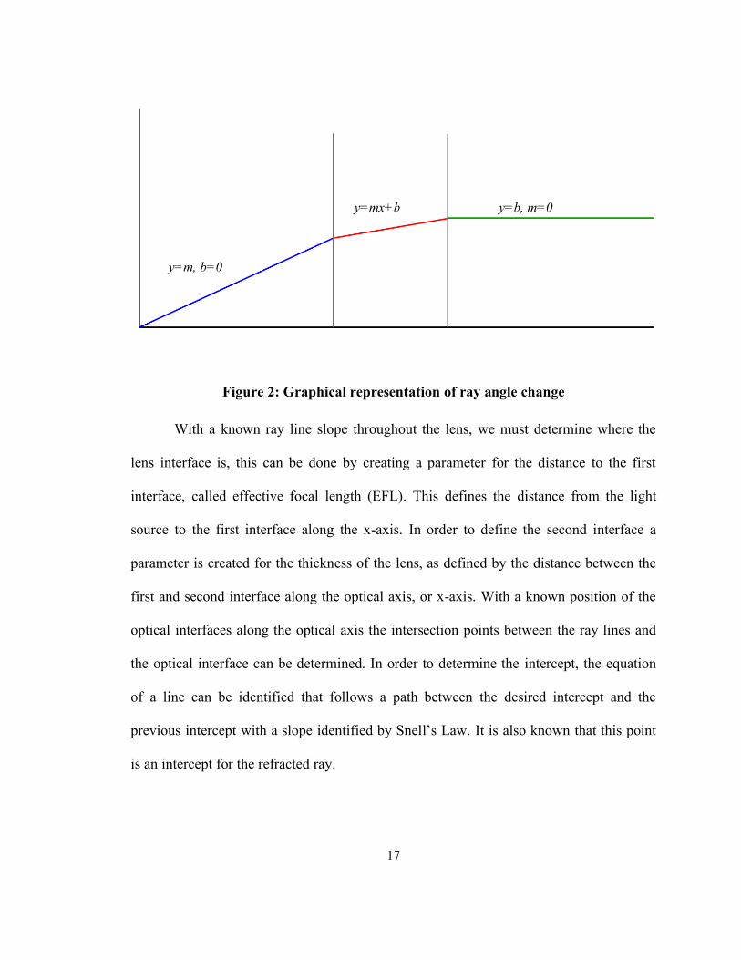
Figure 2: Graphical representation of ray angle change .............................................................. 17
Figure 3: Snell’s Law Example (First Interface left, Second Interface right, Air side red, Acrylic
side blue) .................................................................................................................................. 19
Figure 4: Lens Extrapolation Diagram ....................................................................................... 20
Figure 5: Representation of Equation 35 (left) and Equation 36 (Right) where the red line is the
ray exiting the interface, and the dotted line is the normal to the interface .................................. 32
Figure 6: Representation of Equation 40, Law of Reflection ..................................................... 35
Figure 7: MATLAB Generated Lens Profile .............................................................................. 38
Figure 8: Percent error and Ray Angle ....................................................................................... 40
Figure 9: Percent Error and Lens Profile .................................................................................... 40
Figure 10: Polynomial Generation of First Interface .................................................................. 41
Figure 11: Polynomial Generation of Second Interface .............................................................. 42
Figure 12: Actual vs. Theoretical Lens Shape ............................................................................ 43
Figure 13: Laser Diode Collimation Test with Machined Lens (Left) without Lens (Right) ........ 44
Figure 14: Ray tracing for lens validation .................................................................................. 45
Figure 15: Lumenera Lt425 ....................................................................................................... 46
Figure 16: Laser Collimation Test Setup.................................................................................... 48
Figure 17: Collimated Laser ...................................................................................................... 50
Figure 18: MATLAB Generated Mirror Profile ......................................................................... 53

vii
Figure 19: Mirror Focus Test..................................................................................................... 54
Figure 20: Pulsing circuit diagram ............................................................................................. 58
Figure 21: Multisim Circuit ....................................................................................................... 58
Figure 22: Multisim Oscilloscope Capacitor Discharge ............................................................. 59
Figure 23: Multisim Oscilloscope Pulse .................................................................................... 60
Figure 24: Prototype board design and actual ............................................................................ 61
Figure 25: Transmission Pulse (trigger signal – red, pulse signal – yellow) ................................ 62
Figure 26: Final pulsing circuit board design ............................................................................. 63
Figure 27: Final pulsing board, front (left) and back (right) ....................................................... 63
Figure 28: Reverse Bias Photodiode .......................................................................................... 65
Figure 29: Receiving Circuit board with Reverse Bias Circuit, design (left) and final board (right)
................................................................................................................................................. 66
Figure 30: Face to Face Laser and Receiver (Transmission pulse - channel 1 (yellow), Ground -
channel 2 (blue), Receiver - channel 3 (purple)) ........................................................................ 67
Figure 31: Transmission Pulse (Yellow) and Receiver Noise (Blue) from Oscilloscope ............. 68
Figure 32: Receiver Signal with 60 Hz Noise ............................................................................ 69
Figure 33: Receiver Signal with grounded housing .................................................................... 69
Figure 34: Pre-amplifier (left) and Transimpedance amplifier (right) ......................................... 70
Figure 35: Aluminum foil shielding test .................................................................................... 71
Figure 36: Extended housing isolation test................................................................................. 72
Figure 37: Complete Laser Rangefinder Diagram ...................................................................... 74
Figure 38: Laser Rangefinder Assembly Transparent View of Optical Axis ............................... 76

viii
Figure 39: Laser Rangefinder Assembly Electrical Connections ................................................ 76
Figure 40: State diagram of FPGA Algorithm............................................................................ 79
Figure 41: Error Checking Algorithm Block Diagram ............................................................... 80

ix
List of Tables
Table 1: Comparison of Gimbal Systems and PKM ..................................................................... 3
Table 2: Design Specifications .................................................................................................... 5
Table 3: Specifications of Commercial Laser Rangefinders ....................................................... 10
Table 4: Comparison of Photodiodes ......................................................................................... 64
Table 5: Final Laser Rangefinder Specifications ........................................................................ 84

x
List of Appendices
Appendix A: Mechanical Drawings ........................................................................................... 89

xi
List of Abbreviations and Acronyms
ASIC Application Specific Integrated Circuit
CAD Computer Aided Design
EFL Effective Focal Length
FPGA Field Programmable Gate Array
GaAs Gallium Arsenide
IOR Index of Refraction
MSE Mean Square Error
Nd:YAG Neodymium-doped Yttrium Aluminum Garnet
Op-Amp Operational Amplifier
PIN Positive-Intrinsic-Negative
PKM Parallel Kinematic Mechanism
PLL Phase Locked Loop
RC Resistor-Capacitor
RF Radio Frequency
SWaP Size Weight and Power

1
Chapter 1: Introduction
1.1. Project Background
The Intelligent Sensor Platforms for Unmanned Vehicles project under the
supervision of Dr. Nicholas Krouglicof began at Memorial University in 2010. This
project was the response to a proposal for the development of an opto-electric method of
sense and avoid for unmanned vehicles. Due to changing regulations on the use of
unmanned aerial vehicles in commercial air space there is an increasing demand for a
reliable system that can be used to detect airborne objects, such as commercial aircraft,
and move out of their path of flight. As defined by the U.S. Army Classifies unmanned
aircraft are grouped by maximum payload. The target unmanned aircraft for this project
fits into Group 2 or Group 3 which ranges from 21 to 1320 pounds (9.5 to 599 kg) [1].
Requirements from the nature of these unmanned aircraft insist that payload components,
such as a sense and avoid system, be of low size, weight, and power (SWaP). Dr.
Krouglicof proposed a system in which an intelligent camera would have a fixed field of
view and be able to identify airborne objects within that field of view, this will then
provide the unmanned vehicle with the ability to locate the object in two dimensions,
however to be able to navigate around or away from an object all three dimensions are
needed. In order to determine the depth of the object a second sensor must be used. It was
proposed that a precise high-speed pointing device would be used to move this sensor and
gather the depth information.
2
Typically, in opto-electric aircraft payloads a gimbal based turret system is used,
such as the TASE150 [2], or MicroPOP [3]. Although these systems can be very accurate,
they can consume large amounts of power, be slow moving, and heavy. As an alternative
the project aimed to create a high speed parallel kinematic mechanism (PKM). A PKM
has many advantages over a gimbal, as it has a much lower moving mass, therefore
requiring less power, and is able to achieve faster speeds. Another alternative to a gimbal
or a PKM is a fixed radar system which can scan an area for objects such as the
EchoFlight [4]. This provides a convenient package solution with no moving mass,
however has a fixed field of view and limited repetition rate. A comparison of
specifications of gimbal systems performance and a radar solution can be found in Table
1. The project group developed a high-speed linear motor based on voice coil technology
that is capable of sub-micron precision, a velocity of 2 meters per second, and a 6.6
newton per amp force constant within a 12-millimeter stroke. This was then used in a
unique robotic architecture to create two unique PKM devices, one able to move in two
degrees of freedom, and the other in three degrees of freedom. These two devices weigh
less than 2.5 kilograms and are able to achieve over 1000 degrees per second pointing
speed in any direction, maintain a pointing accuracy of a one hundredth of a degree, and
only consume on average seven watts of power. With a pointing device capable of
moving to a new position every 20 milliseconds, it was determined that the sensor needed
to solve the sense and avoid problem would be a time-of-flight laser rangefinder with a
high repetition rate. In comparison to using a second camera for gathering depth

3
information, a time-of-flight laser rangefinder can gather information at a much higher
rate, while maintaining SWaP requirements.
Table 1: Comparison of Gimbal Systems and PKM
Specificatio
n
PKM+LRF TASE150 MicroPOP EchoFlight Units
Pan +/- 32 360 360 120(fixed field
of view)
Degrees
Tilt +/- 32 +23/-203 +30/-90 80(fixed field
of view)
Degrees
Yaw +/- 32 N/A N/A N/A Degrees
Rotation
Rate
630(average)
- 1170(max)
150 100 N/A Degrees/
Sec
Power 0.54(min) -
8(max)
14 (average)
- 22(max)
15-16.8 15(Standby) -
40(Operating)
Watts
Size 137x137x148 122x112x178 104x104x18
0
187x121x40 mm
Weight 2.15 0.9 1.2 0.73-0.817 kg
1.2. Design Requirements
With the determination that a time-of-flight laser rangefinder was needed for the
sense and avoid system, certain design requirements were identified. Table 2 provides a
summary of all design specifications explained in this sections. Based on the settling time
for the pointing device it was found that a repetition rate of at least 50 measurements per
second was required. The pointing device is capable of moving from one position to
another anywhere within the working envelope in 20 milliseconds, therefore a repetition
rate of 50 measurements per second would align with this constraint. The pointing device
also strictly determines the physical dimensions of the rangefinder. As the performance of
the pointing device is affected greatly by the mass of the object mounted on the motion

4
platform, the laser rangefinder cannot exceed a mass of 250 grams. In addition to the
affect of mass on the performance of the pointing device, the inertia of the rangefinder
must be minimized; this corresponds to the mounted height being kept at a minimum. As
well, due to the physical structure of the pointing device the rangefinder must fit within a
circular area 65 millimeters in diameter.
As part of the Intelligent Sensor Platforms for Unmanned Vehicles project a
controller board was developed using a Field Programmable Gate Array (FPGA). This
controller board was used for every device developed within the project in order to ensure
cohesive operation between devices. Therefore, to maintain consistent development this
same board must be used for the development of the laser rangefinder. Utilizing this
board will aid in maintaining the SWaP requirements of the sense and avoid system as
both the pointing device and rangefinder can operate through the same controller board,
simplifying the overall design and minimizing the maximum power used. The use of this
board will also help in communication between the pointing device/rangefinder controller
and the controller of the intelligent camera, which will also be using a board of the same
design.
A critical constraint that is required for the rangefinder is that of the useable
range. As it is intended to be used for a sense and avoid system, measurement at a range
of less than 50 meters is not necessary. The targets of interest and unmanned vehicle itself
will be moving at speeds ranging from 50 meters per second to upwards of 250 meters per
second; therefore within 50 meters it would be too late for a maneuver to avoid collision.
The distance of interest is on the order of 1 kilometer, providing the unmanned vehicle
5
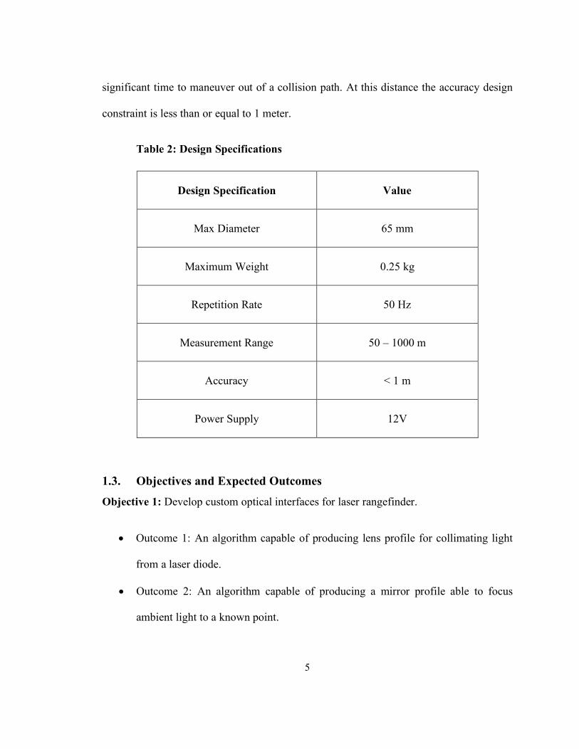
significant time to maneuver out of a collision path. At this distance the accuracy design
constraint is less than or equal to 1 meter.
Table 2: Design Specifications
Design Specification Value
Max Diameter 65 mm
Maximum Weight 0.25 kg
Repetition Rate 50 Hz
Measurement Range 50 – 1000 m
Accuracy < 1 m
Power Supply 12V
1.3. Objectives and Expected Outcomes
Objective 1: Develop custom optical interfaces for laser rangefinder.
• Outcome 1: An algorithm capable of producing lens profile for collimating light
from a laser diode.
• Outcome 2: An algorithm capable of producing a mirror profile able to focus
ambient light to a known point.

6
• Outcome 3: Experimental evaluation of custom designed and manufactured
optical interfaces.
Objective 2: Development of electrical system for laser rangefinder.
• Outcome 4: Hardware implemented pulsing circuit able to meet design
requirements.
• Outcome 5: Hardware implemented receiving circuit able to meet design
requirements.
• Outcome 6: FPGA based controller for interfacing with laser rangefinder.
Objective 3: Development of mechanical structure for laser rangefinder
• Outcome 7: A manufactured laser rangefinder housing meeting design
requirements.
1.4. Thesis Outline
Chapter 1: Introduction – This chapter provides background context to the thesis and
defines objectives for the project.
Chapter 2: Literature Review – This chapter provides a summary of the advancement
of laser rangefinder technology.
Chapter 3: Optical Design – This chapter outlines the algorithms developed to create the
optical system of the laser rangefinder, relating to the first objective and outcomes.

7
Chapter 4: Electrical Design – This chapter details the design and testing of the
electrical systems of the laser rangefinder.
Chapter 5: Mechanical Design – This chapter specifies all mechanical components
required to assemble the laser rangefinder.
Chapter 6: FPGA Design – This chapter specifies the development of the control
algorithm for the laser rangefinder.
Chapter 7: Conclusions – Provides a summary of the thesis and outcomes of the
objectives.

8
Chapter 2: Literature Review
2.1 Laser Rangefinders
In the late 1950’s the ruby laser was invented, paving the way for many further
developments. One such development was the invention of the laser rangefinder. In 1961
the first laser rangefinder was developed, demonstrating the capabilities of the ruby laser.
This system however weighed 90 pounds. Shortly after, in 1966, in the paper “The Laser
Rangefinder”, Hamilton and Fowler describe a portable laser rangefinder system capable
of ranging 10 kilometers with an accuracy of 10 meters, weighing 35 pounds [5]. By the
late 1960’s development of Gallium Arsenide (GaAs) injection lasers were successful,
which provided new methods for laser ranging [6]. The main benefits to the GaAs laser
were the improvement on overall size and weight in comparison to the ruby laser, as well
as high pulse repetition rate. With this configuration, a laser rangefinder was developed
where the total weight was only 9 pounds, 10% of the first laser rangefinder although the
ranging distance was limited to 400 meters. This range finding system described by
Koechner, [6], utilizes a coaxial optical arrangement where the receiving optical axis is
in line with the transmitting optics. This design is achieved through the use of a classic
Cassegrain telescope where the incoming parallel light rays are reflected off of a
parabolic mirror onto smaller hyperbolic mirror centered in the telescope. The hyperbolic
mirror reflects the light rays back to a focal point behind the telescope body [7]. This
telescope design has been in use since the 1700’s when described by Cassegrain and
Newton. This arrangement is popular for maintaining a long optical path in a compact
physical size. The described laser rangefinder places the transmitting laser in front of the

9
hyperbolic mirror, therefore not detracting from any received light, and the receiving unit
is placed behind the Cassegrain telescope collecting light through the focus of the
hyperbolic mirror. This design also utilizes a beam splitter to reflect visible light to a
viewfinder for manual positioning. This beam splitter allows the infrared light from the
transmitter to pass into the receiving unit [6]. Even into the 1980’s GaAs lasers were still
limited to ranging on the order of 100 meters, the common approach for longer range
remained pumped lasers [8], although no longer ruby, typically Nd:YAG.
To show the progression that has been made in laser diode technologies, it can
easily be seen in the 21st century that laser diode rangefinders are readily available at low
cost. These devices can be purchased commercially for uses such as hunting and golfing
such as the Bushnell Legend Rangefinder [9]. This is a point and shoot laser rangefinder
capable of 1000-meter maximum range on a reflective target for a price of 184.00 USD.
In an industrial market, Jenoptik offers laser diode rangefinders with maximum ranges of
20,000 meters [10]. These two examples demonstrate the advancement in laser diodes and
electronics in the last 30 years and a summary of the performance characteristics can be
found in Table 3.

10
Table 3: Specifications of Commercial Laser Rangefinders
Design Specification Bushnell Legend Jenoptik DLEM Units
Size 33x107x74 97x25x50 mm
Weight 0.17 0.095 kg
Repetition Rate N/A 1 Hz
Measurement Range 5 - 1097 10-5000 meters
Accuracy 0.9 1 meters
Power Supply 3 10 Volts
This technology has been further developed into many different forms and uses. In
addition, the methods of Laser Range finding have broadened as range can be determined
based on time of flight sensors, measuring the time it takes for a laser pulse to travel to
and from a target, or the phase shift of a reflected laser pulse can be examined to
determine the range. Applications of this technology have been used to create devices
that can collect data of thousands of points simultaneously, one single point over vast
ranges, or a single point over a very short distance at high precision. The uses for the laser
rangefinders can be found in both military and civilian applications.
2.1.1 Ranging Method
There are two main types of laser ranging methods, time-of-flight and phase shift,
also known as phase modulation. Each of these ranging methods have different strengths
and weaknesses and are used for varying applications.
11
Time-of-flight laser rangefinders utilize time measurement as the source of
distance measurement. The main principal is to time how long it takes a laser pulse to
travel from the source, reflect off of the target, and return to the detector located close to
the source. This type of laser range finder excels at ranging objects at large distances,
upwards of 1 kilometer, while maintaining minimal power consumption. The key factors
to time of flight are ensuring a narrow high-power pulse and a high rate of counting to
maintain precision. In the first laser rangefinders the method in which these lasers were
able to create high power short pulses was through utilizing Q-switching [11]. Q-
switching refers to a technique where laser energy is stored and then released
instantaneously in order to produce high power laser pulses [12]. Q-Switching was
completed through various means including, mechanical, acousto-optic, electro-optic, or
dye switching. An example of mechanical Q-Switching is the use of a rotating mirror
which would shutter the laser light as it leaves a resonating chamber. Utilizing
mechanical methods presented problems due to size and weight limitations, as well as the
maintenance on the device [11]. With advancement in semiconductor lasers there are
many benefits as they are small and efficient and do not require the Q-Switching methods
found with traditional lasers. In place of the Q-Switching methods, a semiconductor laser
can be pulsed with the drive current [8]. This ability significantly improves portability
and maintainability of the laser rangefinder. The counting resolution of early laser
rangefinders consisted of analog counters, an example of which is described by Koechner.
The analog counter consists of a bistable multibibrator, integrating RC network, and four
monostable multivibrators for reset conditions. This counter is triggered by the

12
transmission voltage of the laser and stopped by the reception of the pulse or monostable
multivibrators. The output of the integrating element is fed into an amplifier which
provides the signal to a panel meter [6]. Advances in electronics allowed for the
development of digital counters which utilize a crystal-controlled clock for counting. This
method makes the resolution of the measurement directly related to the clock frequency; a
higher frequency provides a higher resolution. With the development of FPGA devices,
the counter and control method can be housed in a single device with small footprint
compared to the 4 cubic inch size of an analog counter.
An FPGA, or Field Programmable Gate Array, is a form of application specific
integrated circuit that has several thousand usable gate arrays that can be reprogrammed
[13]. This ability provides an opportunity for rapid prototyping and development for
small volume ASICs. Specifically of use in an FPGA is the ability to create multiple
clocks at varying speeds through a phase lock loop (PLL) [14]. Based on the clock of the
system, a PLL can be generated through means such as multiplying or dividing the
system clock, for a laser rangefinder, this allows a transmitting pulse frequency and
timing frequency to both be generated through the same controlling device, providing
synchronization of the start points for the transmission and counter. In addition, the PLL
can be scaled to the maximum available limit of the FPGA to provide optimum timing
resolution.
Phase shift rangefinders function under a different principal than time-of-flight
sensors. In order to determine distance, they emit a source signal in the form of a sine
wave and modulate the frequency and amplitude of the sine wave. The modulated sine
13
wave is reflected off of the target and the returning signal is captured. The reflected wave
will have undergone a phase shift, where the peaks of the sine wave now occur at a
different point. The size of the phase shift is then correlated to a distance [15]. Primary
uses for this type of method include point cloud generation, where an entire scene is to be
captured in a short period of time, such as in architectural heritage scanning [16]. As
phase shift rangefinders must emit a constant signal, the power consumption is higher
than time-of-flight sensors, and the range is limited to the power available.

14
Chapter 3: Optical Design
3.1. Introduction
Through the required constraints on the laser rangefinder for size, weight, and
power, it was decided that an infrared laser emitting diode would be used as the optical
power source. A laser diode was selected based on the optical power output, package size,
and maximum pulsing rate. The laser diode that was chosen was the OSRAM
Semiconductor SPL PL 90_3. This laser diode is capable of a maximum optical output
power of 90 Watts with a wavelength of 905n. It is housed in a standard five-millimeter
diode package and is capable of generating laser pulses from 1 to 100 nanoseconds in
length. There were no other laser diodes that provided comparable performance in this
package. In conjunction with the infrared emitter, the Panasonic PNZ331CL PIN
Photodiode was chosen as the optical receiver. This receiver meets all size, weight, and
power requirements, and a two nanosecond rise and fall time. The benefit of the rise and
fall time will aid in producing accurate return signal identification.
A unique novel arrangement was developed for the laser rangefinder in which all
optical components would exist along the same optical axis. This would be achieved by
developing a combined lens which will provide collimation for the laser diode while
allowing the returning light to pass unaltered through the surrounding area. A focusing
mirror is positioned at the end of the laser rangefinder to direct the returning light onto the
photodiode. Utilizing this coaxial design provides improved alignment of the transmitting

15
and receiving light paths, as well as opportunities to minimize the overall size as a single
lens can be used for two purposes, as opposed to two separate lenses. A generalization of
the coaxial operation of the laser rangefinder can be found in Figure 1, showing the light
path of both the transmitted light and received light though the same lens.
Figure 1: Coaxial Laser Rangefinder Light Path
3.2. Development of Ray Tracing Algorithm for Design of Aspherical
Optical Interface
Ray tracing is based on the assumption that light can be simplified into straight
lines that pass through an optical interface undergoing operations of refraction or
reflection to produce the resultant image [17] . Using this simplification and known light
characteristics, an algorithm can be developed that will define the shape of a lens that is
required to achieve a desired light image. In the case of a laser rangefinder an algorithm
must be made to define a lens with an image that is a spot of collimated light, light rays
that are parallel, and a second algorithm to define a mirror that can focus collimated light
to a specific point.
Transmitted Light Path
Received Light Path
Mirror
Collimating Lens

16
To begin developing an algorithm, the desired light path must be identified. This
may be due to physical constraints on the size of the lens, or light source characteristics.
For the case of a light source, a technical specification sheet can be used to determine the
maximum angle at which light is emitted, therefore providing a maximum ray angle that a
light ray will follow. This also determines the maximum diameter of the lens, as the
diameter will become a function of the largest ray angle and focal length, or distance from
the lens. With the light source known we can define each ray graphically by the linear
equation as shown in Equation 1, where y and x are the radius of the lens and distance
along optical axis on a graph, m is the slope of the line, and b is the y-intercept.
bmxy += Equation 1
In the design of a singular lens, it is known that there will be two optical
interfaces, the first being the intercept of the ray with the lens after it has left the light
source and the second as the ray passes from the lens back into the atmosphere. With two
optical interfaces there will be three different ray line equations, the first being simplified
with the assumption that the origin will act as the light source, removing the y-intercept
(b=0), and the third equation can be simplified to a constant as it is known that the light
will be collimated. As the second ray equation has no specific definition, it must be
constrained. This can be completed by specifying a desired angle change between the first
and second ray. For this algorithm it was chosen that the angle would be reduced by half.
The graphical representation of this is conveyed in Figure 2.
17
Figure 2: Graphical representation of ray angle change
With a known ray line slope throughout the lens, we must determine where the
lens interface is, this can be done by creating a parameter for the distance to the first
interface, called effective focal length (EFL). This defines the distance from the light
source to the first interface along the x-axis. In order to define the second interface a
parameter is created for the thickness of the lens, as defined by the distance between the
first and second interface along the optical axis, or x-axis. With a known position of the
optical interfaces along the optical axis the intersection points between the ray lines and
the optical interface can be determined. In order to determine the intercept, the equation
of a line can be identified that follows a path between the desired intercept and the
previous intercept with a slope identified by Snell’s Law. It is also known that this point
is an intercept for the refracted ray.
y=m, b=0
y=b, m=0 y=mx+b

18
With the design constraints of the ray paths and mediums in which the ray will be
passing known, the required slope for the optical interface along each ray can be
identified through the application of Snell’s Law, Equation 2 Snell’s Law dictates that the
relation of the sines of the input and output ray angles will be proportional to the relation
of the index of refraction of the mediums.
( ) ( )outoutinin nn sinsin =
Equation 2
As Snell’s Law is applied to a flat plane, entry and exit angles are defined relative
to the normal of that flat plane, therefore we can determine the slope of the flat plane,
which is a tangent on the lens interface at the intersection point of each incoming and
outgoing ray line, and the coordinates of the intersection point on this plane. To do this
each ray line slope must be converted to an incident angle to the tangent, and the angle of
the normal to the tangent must be identified in order to relate the slope of the tangent back
to the axis.

19
Figure 3: Snell’s Law Example (First Interface left, Second Interface right, Air side
red, Acrylic side blue)
n1
Air
n2
Acrylic
θ1 θ2
n2
Acrylic
θ2
θ3
n3
Air

20
It is also known that based on the design constraints of moving from a larger to a
smaller slope (angled ray from the source to parallel collimated rays), and that the index
of refraction of the lens medium is greater than that of atmosphere, the first lens interface
will consist of tangents of decreasing positive slope values and the second interface will
be increasing negative slope values, moving through the horizontal optical axis, therefore
simplifying the formulas required in the algorithm.
Figure 4: Lens Extrapolation Diagram
n1
Air
n2
Acrylic
Intersection of tangent
with next intersection
point

21
For a known slope of value m, the angle between the slope and the horizontal can
be defined by the arctan of m. If the design optical axis occurs on the x-axis, the angle
between the first ray and first interface would be equal to arctan of m, α, plus the angle
between the normal of the tangent and the horizontal, βn,
Equation 3.
+= nin Equation 3
In the case of the first interface it is known that the outgoing angle will be equal to
half of the incoming angle relative to the horizontal, γ, as specified by the design
constraints, plus the angle between the normal of the tangent and the horizontal, βn as
described in Equation 4.
+= nout Equation 4
Utilizing Snell’s Law, Equation 2, a new equation can be created by substituting
the constraints for the incoming and outgoing angles as described in Equation 3 and
Equation 4. This substitution creates Equation 5 which can be used to solve for βn through
the use of the Newton –Raphson method.
( ) ( ) +=+ noutnin nn sinsin Equation 5
Newton-Raphson method is an iterative method in which a function is specified,
in this case the function found in Equation 6 is equivalent to Equation 5 rearranged.
( ) ( ) ( ) +−+= ninnoutn nnF sinsin Equation 6

22
Newton Raphson method requires an initial guess of the value of βn, then
increments this value of βn, by a value determined by dividing the solution of the original
function, Equation 6 at the initial guess, by the derivative of the function Equation 7 at the
initial guess.
( ) ( ) ( ) +−+= ninnoutn nnF coscos' Equation 7
Dividing the original function by the derivative, which is equivalent to the slope
of the function at the estimated value, a delta value is identified, dth, as shown in
Equation 8.
( )( )n
nth
F
Fd
'
−= Equation 8
The delta value, dth, is used to increment the value of βn until the delta value is
near zero, defined by 10-6. The iteration equation for βn is found in Equation 9.
thnn d+=+ 1 Equation 9
With the solution of the Newton-Raphson method producing a value of βn, the
normal of the curve of the lens, Equation 10 defines the slope of the tangent to the curve
by taking the inverse of the tangent of βn.
)tan(
1tan
n
m
=
Equation 10
23
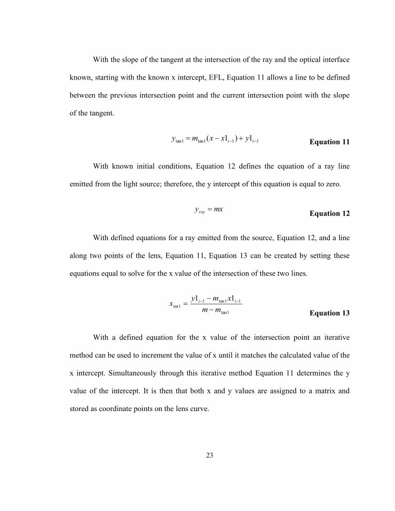
With the slope of the tangent at the intersection of the ray and the optical interface
known, starting with the known x intercept, EFL, Equation 11 allows a line to be defined
between the previous intersection point and the current intersection point with the slope
of the tangent.
111tan1tan 1)1( −− +−= ii yxxmy Equation 11
With known initial conditions, Equation 12 defines the equation of a ray line
emitted from the light source; therefore, the y intercept of this equation is equal to zero.
mxyray = Equation 12
With defined equations for a ray emitted from the source, Equation 12, and a line
along two points of the lens, Equation 11, Equation 13 can be created by setting these
equations equal to solve for the x value of the intersection of these two lines.
1tan
11tan11int
11
mm
xmyx ii
−
−= −−
Equation 13
With a defined equation for the x value of the intersection point an iterative
method can be used to increment the value of x until it matches the calculated value of the
x intercept. Simultaneously through this iterative method Equation 11 determines the y
value of the intercept. It is then that both x and y values are assigned to a matrix and
stored as coordinate points on the lens curve.

24
To calculate the coordinates of the intersection points of the second lens interface
the same Newton – Raphson function is used. The only difference is that arguments are
passed into the function which describes the path of the ray entering and exiting the
second interface, as constrained by design assumptions. The output of the Newton-
Raphson method provides the Normal of the second interface at the intersection point
with the ray which has been refracted by the first interface. Using the same method as
found in Equation 10, the slope of the tangent to the second interface is identified, mtan2.
Equation 14 utilizes the known slope of the curve at the intersection point to define a line
between the intersection point and the previous intersection point.
112tan2tan 2)2( −− +−= ii yxxmy Equation 14
With the design constraint on the slope of the ray leaving the first interface, and
knowing that it intersects the first lens at a defined coordinate, Equation 15 defines the
path of the ray line that exits the first interface after it has undergone the refraction
defined by Snell’s Law.
)(1 2122 mmxxmy iray −+= − Equation 15
In a method similar to that used for the first interface Equation 14 and Equation 15
can be set equal to one another to create Equation 16, which has been rearranged to solve
for the x coordinate of the intersection point of the second interface.
2tan2
2112tan12int
)(122
mm
mmxxmyx iii
−
−−−= −−− Equation 16
25
Through the same iterative process used to identify the coordinates of the first
interface, the values of the x and y coordinates of the second lens interface are also
captured and assigned to a matrix. This is then repeated for a defined number of iterations
to generate a series of points which can be used to determine the polynomial of the curve
of the first and second interfaces through regression.
3.3. Development of ray tracing algorithm for lens validation
With a completed lens design through the algorithm defined in section 3.2, or any
other lens defined by a polynomial, an algorithm can be developed that computes the
effectiveness of the lens for the use of collimation. This algorithm begins with specific
assumptions; that the transmitting source is known, and that it will originate at a known
distance, or within a specified range of distances from the first lens interface and that the
polynomial of the lens interfaces is defined. The purpose of the algorithm is to output a
series of ray angles emitted from the second lens interface and determine how closely
they resemble that of fully collimated light rays.
Similar to section 3.2 Newton – Raphson method can be used, however in this
case, instead of solving for the normal to the curve, it will be used to solve for the
coordinates along the curve in which the ray and the curve intersect. As the polynomial is
known, the outgoing ray angles from both the first and second interfaces can be solved
directly with the solution of Newton Raphson. To solve for the x and y coordinates of the
intersection point, the algorithm utilizes the slope of the ray exiting the light sources as an

26
input, incrementing the slope, and therefore angle, across the first lens interface.
Equation 17 defines the equation of the ray emitted from the source with input slope m,
with a y-intercept value equivalent to the effective focal length, EFL, of the lens, or
distance of the emitter from the first lens interface.
EFLmxy −= Equation 17
To complete the function for Newton-Raphson the polynomial of the lens
interface must be defined. Equation 18 defines the polynomial of the first lens interface,
the constants A, B, and C are inputs of the algorithm.
11
2
11 CxBxAy ++= Equation 18
With both the equation of the incoming ray and the polynomial of the first
interface defined, Equation 19, the Newton-Raphson function can be defined as a matrix
of the two equations with two unknowns.
( )
−−
−++=
EFLyxm
yCxBxAyxF
2
, Equation 19
With the function defined, the derivative must be determined in order to calculate
the delta values for the x and y coordinates based on the initial guess. Equation 20 defines
the derivative of the function in Equation 19, also in the form of a matrix of two
equations.

27
( )
−
−+=
1
12,'
m
BxAyxF Equation 20
With the function and derivative defined, the delta value, dth, of the initial guess
can be determined through Equation 21, in which the function is divided by the
derivative.
( )( )yxF
yxFd th
,'
,−= Equation 21
With the delta value defined, the next iteration of x and y coordinates can be
determined through Equation 22 and repeated until the result of the delta approaches zero.
In the algorithm this point is defined as 10-6.
+
=
th
th
dy
dx
y
x
y
x
int
int Equation 22
With the solution of the coordinates of the intersection point of the first ray and
the first interface, it is now possible to use these values to determine the path of the ray
exiting the first interface. This can be done by rearranging Snell’s Law to solve for the
outgoing angle where the ray is moving from air to the lens medium. To simplify the
equations, a substitution is made in Snell’s Law, Equation 2, using Equation 23 to define
the index of refraction (IOR) as the lens medium divided by the atmospheric medium.

28
atmosphere
lens
n
nIOR = Equation 23
=
IORa I
O
)sin(sin 1
1
Equation 24
We know that when applying Snell’s law to a ray passing through an interface the
angles are relative to the normal of the interface, therefore we must determine the angle of
the normal. It is known that the derivative of a polynomial is equal to the slope of the
polynomial at a given set of coordinates, mtan1, as described in Equation 25. With this
slope identified, we can use Equation 26 defines the angle of the normal from the slope
identified in Equation 25 by taking the inverse of the tan of the slope.
11int11tan 2 BxAm += Equation 25
)tan( 1tan1 ma= Equation 26
With the assumptions made that the location of the light source is known the slope
acts as an input in the algorithm, and therefore Equation 27 defines the angle of the ray
entering the first interface, γ1, based on the input slope, m.
)tan(1 ma= Equation 27
As stated, Snell’s law requires that input and output angles be defined relative to
the normal of the lens interface. Equation 28 provides the angle of the ray entering the
first interface relative to the normal of the first interface β1 and Equation 29 defines the
angle of the ray exiting the first interface relative to the normal of the first interface.
111 90 +−=I Equation 28

29
1190 Oray −+= Equation 29
With the angle of the outgoing ray defined the slope can also be determined
through Equation 30. With the slope defined an equation of the path of the ray exiting the
first interface can be created in the form of a linear equation, Equation 31. Knowing that
this line passes through the intersection point of the first ray and the first interface it is
possible to solve for the y-intercept, bray.
)tan( rayraym = Equation 30
1int1int xmyb rayray −= Equation 31
Having fully defined the equation of the ray exiting the first interface and having
the polynomial constants of the second interface defined through inputs of the algorithm,
the Newton-Raphson function previously described can be reused. The only condition is
that instead of utilizing the variables for the linear question of the first ray, slope and y-
intercept, now the variables for the second ray are substituted. The output of the Newton-
Raphson function will provide the x and y coordinates of the intersection point of the ray
exiting the first interface and the second interface.
Similarly to identifying the angle of the ray exiting the first interface, the angle
exiting the second interface can be determined through Equation 32, which rearranges
Snell’s Law to solve for the outgoing angle where there is a transition from the lens
medium back to air.
( ))sin(sin 22 IO IORa = Equation 32
30
Again, as Snell’s Law requires all angles to be relative to the normal of the lens
interface the normal to the lens must be determined at this intersection point. This can be
completed by solving for the derivative of the polynomial of the second lens interface,
Equation 33, which is equivalent to the slope, and then taking the inverse tan of this to
provide B2 as found in Equation 34.
22int22tan 2 BxAm += Equation 33
)tan( 2tan2 ma= Equation 34
As this algorithm has the intent of determining the difference between the
outgoing ray and a perfectly collimated ray, in the case of this algorithm an angle of 90
degrees, two conditions had to be generated when determining the final output angle
based on the normal to the second lens interface. One in which the angle of the normal to
the lens interface is greater than that of the incoming ray, Equation 35, and one in which
the angle of the normal is less than that of the incoming ray, Equation 36. The angles of
the normal and ray are all relative to the horizontal plane, or x axis. This is important in
determining the angle of the outgoing ray relative to the horizontal for output and
analysis. If the incorrect condition was used it would provide a false value of the angle of
the outgoing ray.
)90(22 rayI −−= Equation 35
)90(22 rayI −+−= Equation 36

31
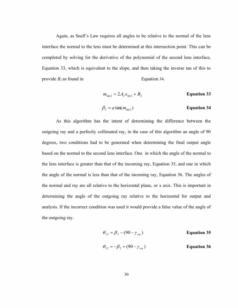
The two conditions of the outgoing ray angle can be represented in Figure 5. In
this figure the solid black line is the lens interface, the blue line is the path of the ray
which has exited the first interface and is passing through the second interface, the red
line is the ray exiting the second interface, and the dashed line represents the normal to
the second lens interface. The depiction on the left represents the case of Equation 35,
where the angle of the normal is greater than that of the incoming ray relative to the
horizontal. The depiction on the right represents Equation 36 where the angle of the
normal is less than that of the incoming ray relative to the horizontal.
32
Figure 5: Representation of Equation 35 (left) and Equation 36 (Right) where the
red line is the ray exiting the interface, and the dotted line is the normal to the
interface
n3
Air
n2
Acrylic
θ3
θ2
θ2
θ3
n3
Air
n2
Acrylic

33
With the outgoing ray calculated, this entire process is iterated through a specified
number of incoming ray slopes over a specified number for focal lengths to determine
which focal length will best suit the designed lens.
3.4. Development of ray tracing algorithm for Aspherical Mirror
The development of an algorithm for an aspherical mirror was completed
similarly to lens design algorithm described in section 3.2. Using the mathematical
modelling software MATLAB, an algorithm was written that would determine the ideal
curve for a mirror that would reflect incoming infrared light to a single point aligned with
the optical axis of the mirror at a specified distance. The algorithm provides the ability to
customize of the mirror shape based on the distance of the focus point from the surface of
the mirror, diameter of area blocked by electronics for the receiving circuit and desired
outer mirror diameter. As with the collimating lens design, incoming and outgoing ray
characteristics are also known for the mirror.
For the development of the algorithm it is being assumed that incoming rays of
light will be parallel with the optical axis of the mirror. This assumption has been made
based on a diffuse or Lambertian reflection of the transmitted light from the target object.
A diffuse reflection implies that the light energy from the transmission will be equally
distributed radially outward from the point of reflection. Based on this assumption light
rays will be reflected parallel to the light transmitted and return to the laser rangefinder in
this pattern. Using this assumption, it is possible to define Equation 37, the path of the
incoming light ray, as a constant.

34
by inray =_ Equation 37
The algorithm identifies the x and y coordinates of points along the mirror surface
by solving the equation of the intersection of the ray of light entering the mirror and a line
defined by the previous mirror point and the slope of the mirror at that point. As the ray
entering the mirror is a constant parallel to the horizontal as defined in Equation 37. This
value will act as an input to the algorithm and be incremented through a loop. Therefore
Equation 38 can be used to make the assignment of this ray equivalent to the y value of
the intersection point of the mirror.
inrayi yy _= Equation 38
Utilizing the design constraints and required inputs to the algorithm, such as
distance between the mirror and the receiver and the radius at which the mirror curvature
begins, the first x and y intercepts are known. With this initial condition Equation 39 can
be used to solve for the next x coordinate of the intersection point of the incoming ray and
the mirror.
1tan
1tan11
−
−−− +−=
i
iiii
im
mxyyx
Equation 39
The collimating lens algorithm used Snell’s Law to determine the relationship
between incoming and outgoing rays of light; similarly the mirror algorithm is based on
the law of reflection, Equation 40, in which the incoming angle is equivalent to the
outgoing angle relative to the surface normal.
35
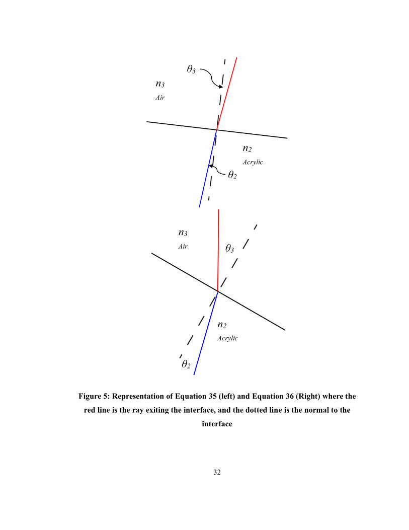
outin = Equation 40
This implies that the slope of the ray relative to the normal of the intersection
point of the mirror will be equivalent for the incoming and outgoing rays as represented
by Figure 6. Knowing that the incoming ray is parallel to the optical axis, the horizontal,
the slope of the outgoing ray is equivalent to the twice the slope of the normal. Assigning
design constraints can provide enough information to specify the slope of the first ray
between the focal point and the mirror can be determined. Equation 41 defines the path of
a ray between the mirror and the receiver.
ray
raym
EFLxmy −= Equation 41
Figure 6: Representation of Equation 40, Law of Reflection
θ
θ
Mirror
Air
36
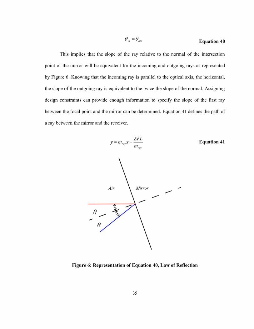
To solve for the angle of the normal Equation 41 can be rearranged to solve for the
slope of the ray path between the mirror and receiver, Equation 42. Then by applying the
fundamentals of the law of refraction, Equation 43 calculates the angle of the normal by
finding half of the arctangent of the slope of the ray.
EFLx
ym
i
iray
−=
Equation 42
( )2
tan ray
norm
ma= Equation 43
With the angle of the normal defined it is possible to identify the slope of the
tangent to the mirror at the intersection point. Equation 44 shows that this is calculated by
the inverse tangent of the angle of the normal.
)tan(
1tan
norm
m
−= Equation 44
3.5. Design of Transmitting Optics
In order to design the lens for the laser rangefinder, the algorithm described in 3.2
was written that would generate the required lens shape for specified incoming and
outgoing light characteristics. As the laser diode that will be used is known, it can be
assumed that the laser light is being emitted from a point source, as the emitter is quoted
at 2000 square micrometers. The laser diode also specifies that the output characteristics
of the laser, or beam divergence, are 9 degrees parallel to the emitter and 25 degrees

37
perpendicular to the emitter. Therefore, using the largest beam divergence of 25 degrees,
the first optical interface of the lens will have to accept point source emitting light rays at
a divergence of 25 degrees. Similarly, since it is desired that the output of the lens should
consist of collimated light, the light rays leaving the lens, or the second optical interface,
should be parallel. With the input and output characteristics of the lens known, the only
other requirements are to specify the distance of the point source from the first interface,
the desired thickness of the lens, and how the light rays inside of the lens will be treated.
The distance of the point source, as well as the thickness of the lens can be changed to
meet the physical design requirements of the laser rangefinder.
Another required input for the algorithm is for the index of refraction of the
medium in which light will pass through in order to satisfy Snell’s Law. It will be
assumed that the laser rangefinder will only be used in earth’s atmosphere, therefore the
index of refraction is 1.0 and the second medium will be acrylic, which has an index of
refraction of 1.48 [18]. Acrylic was chosen as the lens material for the physical properties
of clarity, weight, and machinability.

38
Figure 7: MATLAB Generated Lens Profile
In order to calculate the accuracy of the lens design the lens validation algorithm
described in 3.3 was used. In this algorithm the angle of the outgoing ray calculated for
each ray leaving the lens for a series of given focal lengths and then stored in a matrix.
This matrix is then exported from MATLAB and manipulated in Excel to provide the
mean square error, MSE, for each focal length. This was completed by subtracting the
angle of the ray from 90 degrees to obtain the error in each ray, squaring this value and
then for each focal length taking a sum of all ray errors and dividing by the number of
rays as shown in Equation 45. The standard deviation of the square error was also
39
calculated and the focal length which provided the minimum mean square error and
standard deviation was identified.
( )=
−=
n
i
ray
n
iMSE
1
2
290
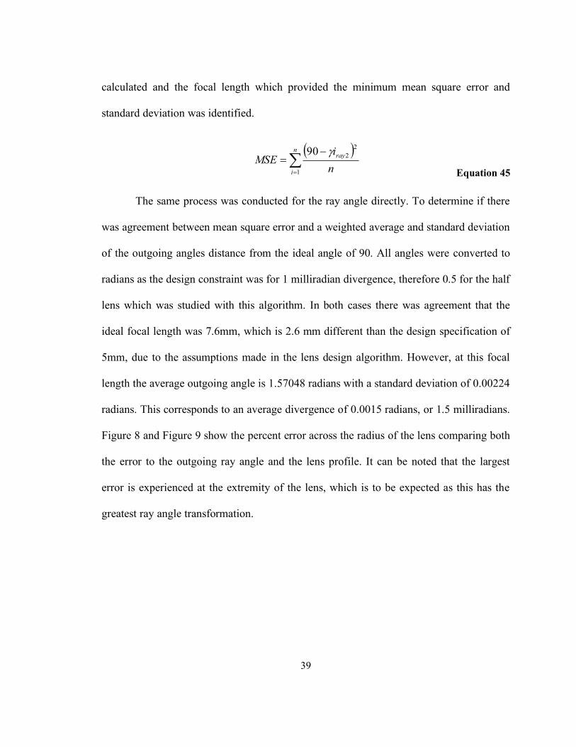
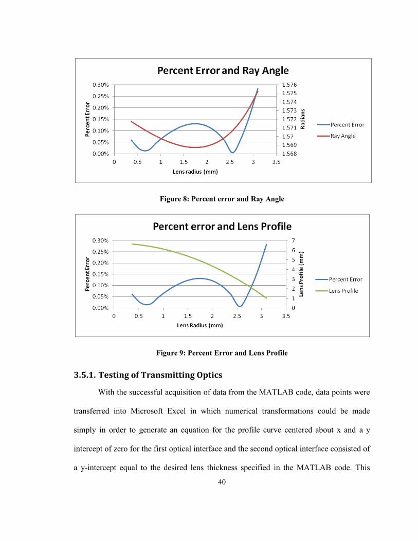
Equation 45
The same process was conducted for the ray angle directly. To determine if there
was agreement between mean square error and a weighted average and standard deviation
of the outgoing angles distance from the ideal angle of 90. All angles were converted to
radians as the design constraint was for 1 milliradian divergence, therefore 0.5 for the half
lens which was studied with this algorithm. In both cases there was agreement that the
ideal focal length was 7.6mm, which is 2.6 mm different than the design specification of
5mm, due to the assumptions made in the lens design algorithm. However, at this focal
length the average outgoing angle is 1.57048 radians with a standard deviation of 0.00224
radians. This corresponds to an average divergence of 0.0015 radians, or 1.5 milliradians.
Figure 8 and Figure 9 show the percent error across the radius of the lens comparing both
the error to the outgoing ray angle and the lens profile. It can be noted that the largest
error is experienced at the extremity of the lens, which is to be expected as this has the
greatest ray angle transformation.
40
Figure 8: Percent error and Ray Angle
Figure 9: Percent Error and Lens Profile
3.5.1. Testing of Transmitting Optics
With the successful acquisition of data from the MATLAB code, data points were
transferred into Microsoft Excel in which numerical transformations could be made
simply in order to generate an equation for the profile curve centered about x and a y
intercept of zero for the first optical interface and the second optical interface consisted of
a y-intercept equal to the desired lens thickness specified in the MATLAB code. This

41
equation was then transferred to the 3D Computer Aided Design software Solidworks.
Utilizing the ability to create an equation driven curve in a sketch feature, the exact lens
profiles were duplicated. To create a 3D part from this sketch the profiles were rotated
about a central axis, collinear with the optical axis. Additional features were added to the
lens in order to provide structural mounting features, as well as create the pass-through
lens allowing light to reach the receiver mirror.
Figure 10: Polynomial Generation of First Interface

42
Figure 11: Polynomial Generation of Second Interface
With a completed part design, the file was then sent to a machine shop for
production. Upon receipt of the completed lens a test was conducted in order to determine
the accuracy of the machining process. Using the Zeiss O-Inspect Coordinate
Measurement Machine in the Mechatronics Development and Prototyping Facility at
Memorial University, measurements on the order of a micron were taken of the lens.
Analysis of these measurements indicated that the profile that was manufactured did not
match that generated in modelling software. Measurements of the lens were taken along
two perpendicular axes across the second interface and the flat plane of the lens was used
as a reference for a base plane. Due to the available measurement probes on the O-Inspect
Machine, the first interface could not be measured. The smallest probe diameter could not
measure the transition in curvature of the lens. The measurements were plotted in
Microsoft Excel and compared to the theoretical curve specified by the lens design. The

43
results indicated that the top portion of the lens appeared to be flattened, potentially from
the hand polishing process and that the polynomial curve varied throughout the lens.
Figure 12: Actual vs. Theoretical Lens Shape
To test the optical characteristics of the lens a 3D printed mount was created to
position a laser diode the correct distance from the lens. A camera with the infrared filter
removed was mounted next to the lens and both were positioned facing a planar surface 2
meters away. The laser diode was set to pulse a 50ns laser pulse at a frequency of 50
hertz, while the camera had a ten thousand millisecond exposure time. At a 2-meter range
a successful laser collimation lens would produce a spot approximately equal to the
diameter of the collimating lens, for this case six millimeters. The spot that was captured
by the camera was approximately 150-200 millimeters in diameter. When the same test

44
arrangement was used without a collimating lens the spot size was approximately 900
millimeters along the widest axis.
Figure 13: Laser Diode Collimation Test with Machined Lens (Left) without Lens
(Right)
Recognizing that it may not be feasible to produce a lens to the desired
specifications, MATLAB was used to simulate what focal length would provide the
optical collimating characteristics based on the measurements from the physical lens. The
known measurements from the physical lens would undergo transformations in Microsoft
Excel in order to generate a polynomial equation for each interface in relation to the
desired configuration used to design the lens. Using the algorithm described in section
3.3, the angle of the final output ray lines and identifying the mean square error of the
difference from the design target of collimated ray lines for each tested focal length, the
optimal focal length can be found. Figure 14 shows the graphical output of the lens
validation algorithm for a single focal length, some of the output rays appear reflected
downward, however this implies that the output angle is greater than 90 degrees, or
vertical.
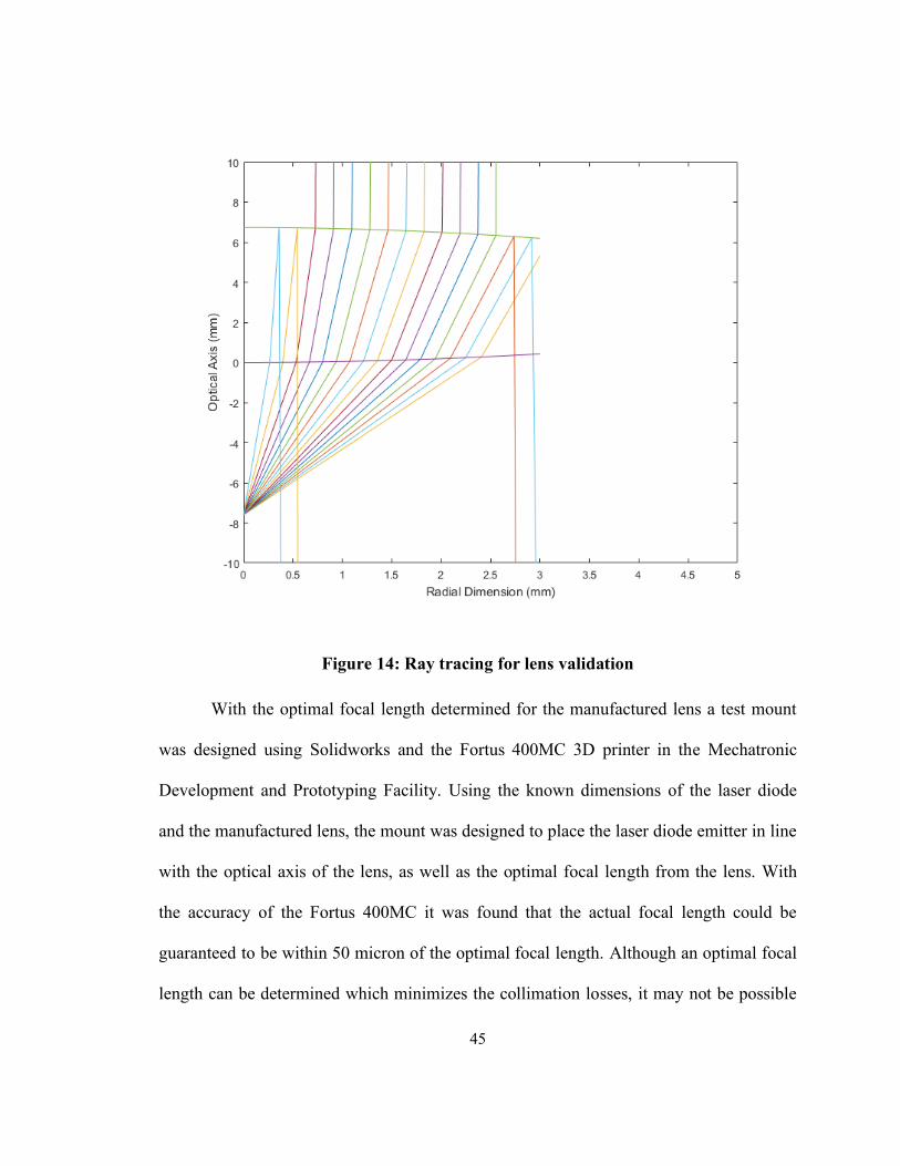
45
Figure 14: Ray tracing for lens validation
With the optimal focal length determined for the manufactured lens a test mount
was designed using Solidworks and the Fortus 400MC 3D printer in the Mechatronic
Development and Prototyping Facility. Using the known dimensions of the laser diode
and the manufactured lens, the mount was designed to place the laser diode emitter in line
with the optical axis of the lens, as well as the optimal focal length from the lens. With
the accuracy of the Fortus 400MC it was found that the actual focal length could be
guaranteed to be within 50 micron of the optimal focal length. Although an optimal focal
length can be determined which minimizes the collimation losses, it may not be possible
46
to orient the lens to provide the desired collimation characteristics. In order to determine
the collimation characteristics of the lens a test was developed utilizing a camera image
capture system.
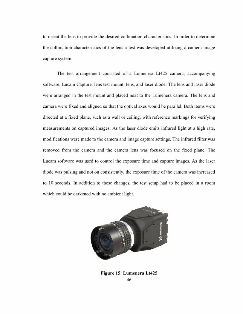
The test arrangement consisted of a Lumenera Lt425 camera, accompanying
software, Lucam Capture, lens test mount, lens, and laser diode. The lens and laser diode
were arranged in the test mount and placed next to the Lumenera camera. The lens and
camera were fixed and aligned so that the optical axes would be parallel. Both items were
directed at a fixed plane, such as a wall or ceiling, with reference markings for verifying
measurements on captured images. As the laser diode emits infrared light at a high rate,
modifications were made to the camera and image capture settings. The infrared filter was
removed from the camera and the camera lens was focused on the fixed plane. The
Lucam software was used to control the exposure time and capture images. As the laser
diode was pulsing and not on consistently, the exposure time of the camera was increased
to 10 seconds. In addition to these changes, the test setup had to be placed in a room
which could be darkened with no ambient light.
Figure 15: Lumenera Lt425

47
Based on standard laser collimation characteristics achieving one milliradian of
beam divergence, it would be expected that if the lens performed as designed the spot size
at 1 meter would be equal to the diameter of the collimating lens plus two millimeters.
(tan(0.001)*1m=0.001m). With a lens diameter of approximately three millimeters, the
spot size should be five millimeters. It was found that the lens produced a spot that was
110 millimeters at 1.5 meters. This value correlates to a beam divergence of 36
milliradians. As the tested beam divergence deviated greatly from that of the theoretical,
it was determined that with the provided resources it was not possible to develop a
customized collimating lens and that an alternative solution would have to be developed.
3.5.2. Alternative Transmitting Optics
Through design and testing it was found that due to limitations in the
manufacturing processes available a feasible lens could not be produced. Future work
may be completed with the implementation of precision machining practices, however, to
complete the remainder of the work a standard collimating lens was purchased from
Edmund Optics, lens 64-799. In order to still achieve the design requirements of collinear
optical axis for the transmitting and receiving optical paths a single lens was
manufactured from the purchased lens and a piece of optically clear cast acrylic. A circle
of the required diameter was cut from a sheet of the acrylic with the use of a TROTEC
laser cutter in the Mechatronic Development and Prototyping Facility. A hole was then
precisely machined with an M9x0.5 thread at the center to receive the mount on the
purchased lens. This would provide for adjustment of the purchased lens to identify the
optimal focal point.

48
Figure 16: Laser Collimation Test Setup
Lumenera Lt425
FPGA
Laser Rangefinder
Power Supply
Target Surface

49
To ensure proper collimation of the laser, a test setup was created with the use of a
Lumenera camera. The camera would be used to detect the laser spot on an object while
the focal length was adjusted, providing the ability to accurately tune the collimation. The
test setup consisted of the Lumenera camera pointed at a white box, the laser rangefinder
pointed at the same white box from a distance of 2 meters, the equipment required to
power the laser rangefinder, and a laptop to view the camera images, as shown in Figure
16. To first ensure the functionality of detecting the infrared laser the camera was pointed
directly at the transmitter and the laser was visible. The next step was to see if the laser
spot could be detected on the surface of the white box. Initially, the spot was not
collimated the spot was not visible with the Lumenera camera and the lab lights had to be
turned off. With the lights turned off, the spot was collimated utilizing the thread on the
collimating lens to identify the optimal focal length. The lights were then turned back on
and the spot was highly visible as indicated by Figure 17. It can be noted that there are
three distinct lines of collimated infrared light. Each of these lines corresponds to an
infrared emitter found in the laser diode used in the transmitting electronics, the OSRAM
SPL PL90_3. This laser diode consists of three epitaxially emitters, where three 25W
emitters are stacked to create one 75W laser diode.

50
Figure 17: Collimated Laser
3.6. Design of Receiving Mirror
3.6.1. Light Energy Dissipation
In order to apply the lens generating algorithm described in section 3.4, a diameter
of the overall mirror must be known. The size of the mirror will be restricted by the
amount of light energy required by the receiver to generate a signal. Equation 46 was
used to determine the size that was required for the receiving optics. This equation was
defined by Nejad et al [19] and determines the amount of optical power that would be
returned to the laser rangefinder receiving optics.

51
opti Pr
rAP
2
)2exp(−= Equation 46
It is required to obtain the absorption coefficient (α), or atmospheric extinction
coefficient to determine the calculation of returned optical power. Wojtanoski [20] et al
studied the atmospheric extinction coefficient for 905 nm lasers in the application of laser
rangefinders and found that over a range of varying relative humidity, the coefficient was
on average 2.3 Km-1 for the worst case scenario of only 1 kilometer visibility. As one of
the design constraints was to achieve 1 kilometer ranging and that since the initial
intention of this project was to pair the laser rangefinder with a vision system, the object
targeted will need to be visible within that range. Therefore, infrared transmission through
cloud and adverse atmospheric conditions can be ignored for visibility of less than 1
kilometer. It was assumed that the total transmission loss (τ) would be 0.75, as combined
from the transmission medium and lens medium and that the total target reflection loss (ρ)
is 1% as used by Nejad et al [19].
Using an iterative method in Microsoft Excel, the reception power was calculated
for varying distances (r), optical power output (Popt), and target object size. Based on the
theoretical beam divergence of the designed lens, if the target object was larger than the
beam, 100 percent of the beam would be returned; otherwise the reflected beam would be
reduced by the fraction of the target area to the diverged beam area for the given distance.
Once the returned optical power was calculated for a variety of distances, the values were
then used to determine the minimum receiving optics that could be used. Similarly, the
received optical energy into the laser diode would be based on a reduction of the returned

52
light energy area and the area of the receiving optics (A), under the assumption that the
designed mirror focused 100 percent of incoming light onto the photodiode. Using the
datasheet from the photodiode the minimum requirement for received light can be
determined, and therefore the size of the laser rangefinder can be scaled to identify a
minimum size.
Although the initial design constraint was to make the laser rangefinder as small
and light weight as possible to meet SWaP requirements, it was chosen to design the test
laser rangefinder much larger than the minimum design requirement in order to simplify
testing. The chosen mirror diameter was 50mm, this was then used in the algorithm to
determine the coordinates of the mirror surface, generating the curve found in Figure 18.

53
Figure 18: MATLAB Generated Mirror Profile
3.6.2. Testing of Mirror
Using the same methods as with the collimating lens, the data from the MATLAB
program was transferred into Microsoft Excel. The data was then manipulated in order to
fit a parabolic curve, however in this case the point of intersection with the x-axis was not
at 0, but at a point equal to the radius of the specified area that was blocked by
electronics. This equation was then used in Solidworks to create a 3D CAD model of the
mirror. This provides the ability to add features to simplify the machining and testing
processes. With a complete 3D CAD model, a drawing was created, and both the part and
drawing were given to a machine shop for manufacture.

54
Although manufacturing flaws were identified with the production of the
collimating lens, the manufacture of the mirror was attempted. As the light source is
infrared light, a material would be required that is capable of reflecting the maximum
percentage of infrared light. It was found that gold has a reflectivity coefficient greater
than 95% for infrared light [21]. As it is impractical to manufacture the entire lens out of
gold, it was determined that a gold coating could be placed on the surface of any material
through the process of gold sputtering, commonly used for providing a metallic coating to
non-metallic parts used in scanning electron microscopes. Therefore, aluminum was
chosen as the medium for the mirror due to the ease of availability and machining
characteristics. Through this method a coating of 76.7 nm thick was applied. This was
completed in two coatings of 38.3nm and 38.4 nm.
Using the O-Inspect Coordinate Measurement Machine in the Mechatronics
Development and Prototyping Facility the accuracy of the machining process was able to
be verified. Unlike the manufacture of the collimating lens which had significant
machining error, the mirror was nearly a match to the specified design and differed by an
average of five percent error. It was found that the error tended to increase towards the
center of the mirror. Feedback from the machinist indicated that this may be preventable
with slight changes to the design of the mirror. The design included a flat portion at the
center where the mirror is blocked by electronics. This provided difficulty for the tooling
to continue the required radius where the curve met the flat point.

55
Figure 19: Mirror Focus Test
A test was conducted where the ability to focus the mirror was realized by using a
sacrificial circuit board for the photodiode and drilling a hole in place of the photodiode.
A small piece of opaque material such as paper was then fixed over this hole. With the
laser rangefinder assembled, visible light could be shone into the laser rangefinder. This
configuration allows the focused spot of the mirror to be visualized by the observer. In
Figure 19 the focused spot can clearly be identified on the paper. The mirror focus could
then be adjusted to minimize the spot size for maximum optical energy, taking into
account the offset distance of the photodiode from the surface of the circuit board.

56
Chapter 4: Electrical Design
4.1. Introduction
Based on the requirements to design a laser rangefinder that would meet Size
Weight and Power requirements it was known that a compact, minimal electronics design
would be required. By utilizing surface mount technology, a circuit of a few components
would be able to fit within a small footprint, reducing the constraint the electronics would
have on the overall size of the laser rangefinder. The majority of the computation required
for triggering and timing the laser pulse would be completed in a Field Programmable
Gate Array, greatly reducing the number of components required in the overall design.
This also provided the capability of off board processing, meaning that the only functions
that would need to be completed on the laser rangefinder itself would be the pulsing and
receiving functions.
4.2. Pulsing Circuit
4.2.1. Design
It was known that in order to achieve an accurate pulse, the integrity of the pulse
generated would need to be maintained through consecutive pulses in addition to creating
a high peak current to produce sufficient optical power for the pulse to transmit the
desired distance of one kilometer. Wang Qing et al in the paper Design of High Peak
Current and Narrow Pulse Driver [22] define a circuit to generate a narrow high peak
current pulse through the use simple electronic components. As an FPGA is being utilized
to generate the trigger pulse a portion of the circuit can be removed for simplification.

57
The Wang Qing design utilizes an N-Channel and P-Channel mosfet combination to
provide the switching function to pulse the laser diode. Similarly a circuit proposed in the
document “Drive Electronics for Pulsed Laser Diodes: Power Where it Matters” [23]
which utilizes a BJT instead of mosfets and a different diode orientation. By combining
each of these circuits a pulsing circuit, Figure 20, was able to be created that would
generate a narrow pulse with a minimal number of components. Through simulation of it
was found that the required peak current to produce sufficient optical power was not
being achieved with a single mosfet, therefore a second mosfet was added in parallel with
the first mosfet. These would receive the same trigger signal, switching at the same time,
therefore increasing the current drain that will pass through the laser diode, in turn
increasing the current optical power.

58
Figure 20: Pulsing circuit diagram
4.2.2. Simulation
The pulsing design was thoroughly simulated with the use of the National
Instruments software Multisim [24]. This software provided the capability of using exact
pSpice models of the electrical components to simulate the real-world environment. This
provides the flexibility of adding components and simulating the impact of different
mosfets or diodes without the need to purchase and test each component increasing
certainty in the chosen components. The effect of changing a mosfet or diode can be
quantified by measuring the difference in peak current of the output pulse. To measure
the peak current, the voltage drop is measured across the 0.1 ohm resistor and the
amperage is calculated.

59
Figure 21: Multisim Circuit
In addition to the need for a high peak current output pulse, it was required that
the pulsing circuit could meet the requirement for high rate of repetition. The design
requirement was a minimum of 50 Hz, indicating that the circuit must create the same
pulse at a minimum repetition rate of every 20 milliseconds.

60
Figure 22: Multisim Oscilloscope Capacitor Discharge

61
Figure 23: Multisim Oscilloscope Pulse
4.2.3. Testing
A prototype board was developed to test the ability of the circuit to create the
required pulse. The purpose of this board was to identify any issues with the circuit in
practical use, and therefore overall size or positioning of the components was not
considered. The optimization of surface area would be completed for the final board.

62
Figure 24: Prototype board design and actual
The prototype board was connected to the FPGA board to provide the pulse
trigger signal and the voltage across a 0.1-ohm resistor in line with the diode was
measured using an oscilloscope. Figure 25 shows the oscilloscope output of the prototype
board transmission pulse across the resistor.

63
Figure 25: Transmission Pulse (trigger signal – red, pulse signal – yellow)
With successful implementation of pulsing circuit, a board revision was made
taking into consideration the size and shape required to fit in the final housing design.
This design stressed the importance of minimization of components and utilizing every
available space on the board. The final design was able to accommodate all the required
components on a double-sided board with 0.0002676 m2 area in the optical field of view,
of which most was occupied by the laser diode. The final design can be viewed in Figure
26 where the dotted lines represent the ground and power plane outlines.

64
Figure 26: Final pulsing circuit board design
Figure 27: Final pulsing board, front (left) and back (right)

65
4.3 Receiving Circuit
4.3.1 Design
The receiving circuit that was used for preliminary testing of the laser rangefinder
was a reverse biased photodiode, implying that the diode is grounded through a resistor,
when photocurrent is received a current is generated, producing a signal that can be
picked up by the FPGA, this circuit can is represented in Figure 28. The chosen
photodiode was the Panasonic PNZ331CL [25], the datasheet for this photodiode
provides the reverse bias circuit as a suggested method of signal capture. This photodiode
was chosen as the peak wavelength of sensitivity is 900 nm and the photodiode emits a
wavelength of 905nm. The physical characteristics of this photodiode also allow for ease
of alignment in the designed circuit boards as it is has through-hole mounting. A
comparison table of other photodiodes can be found in Table 4.
Table 4: Comparison of Photodiodes
Parameter
Panasonic
PNZ331CL
Vishay
TEMD1040
Optek
OPF480
Units
Maximum Operating Voltage 30 60 5(typ.) V
Photo Current 14 10 5 µA
Peak Sensitivity Wavelength 900 940 905 nm
Response Time 2 4 2 ns
Acceptance Half Angle 70 15 40 degrees
Photodetection sensitivity 0.55 0.6 N/A A/W

66
Utilizing the calculations from 3.6.1 and the photocurrent characteristics of the
photodiode it was predicted that the reverse diode circuit design, combined with sufficient
isolation and accurate optical design, would result the laser pulse saturating the
photodiode, creating adequate feedback current.
Figure 28: Reverse Bias Photodiode
With the chosen photodiode and circuit, a receiving circuit board was developed.
This board used the same physical outline as the transmitting circuit board to ensure
consistency in the optical path of returned light.

67
Figure 29: Receiving Circuit board with Reverse Bias Circuit, design (left) and final
board (right)
4.3.2 Testing
Initial testing was completed by placing the laser diode directly face to face with
the photodiode. The goal of this test was to identify a baseline that the photodiode could
saturate with the laser diode. In this test the laser diode and photodiode were connected to
separate power supplies. Figure 30 clearly indicates that in this arrangement, when the
laser is pulsed the receiver saturates.
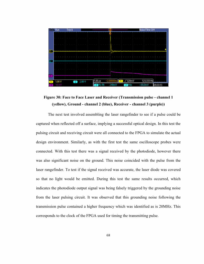
68
Figure 30: Face to Face Laser and Receiver (Transmission pulse - channel 1
(yellow), Ground - channel 2 (blue), Receiver - channel 3 (purple))
The next test involved assembling the laser rangefinder to see if a pulse could be
captured when reflected off a surface, implying a successful optical design. In this test the
pulsing circuit and receiving circuit were all connected to the FPGA to simulate the actual
design environment. Similarly, as with the first test the same oscilloscope probes were
connected. With this test there was a signal received by the photodiode, however there
was also significant noise on the ground. This noise coincided with the pulse from the
laser rangefinder. To test if the signal received was accurate, the laser diode was covered
so that no light would be emitted. During this test the same results occurred, which
indicates the photodiode output signal was being falsely triggered by the grounding noise
from the laser pulsing circuit. It was observed that this grounding noise following the
transmission pulse contained a higher frequency which was identified as is 20MHz. This
corresponds to the clock of the FPGA used for timing the transmitting pulse.

69
Figure 31: Transmission Pulse (Yellow) and Receiver Noise (Blue) from Oscilloscope
It was also observed that the receiver signal appeared to have a wavering
component. The background voltage level measured from the receiving circuit would
increase and decrease. When the time scale of the oscilloscope was increased it became
apparent that there was 60 Hz interference on the receiving circuit, as shown in Figure 32.
It was found that this could be removed by connecting the rangefinder housing to ground.
In future development this could be incorporated directly into the housing design. The
results of grounding the housing are found in Figure 33.

70
Figure 32: Receiver Signal with 60 Hz Noise
Figure 33: Receiver Signal with grounded housing
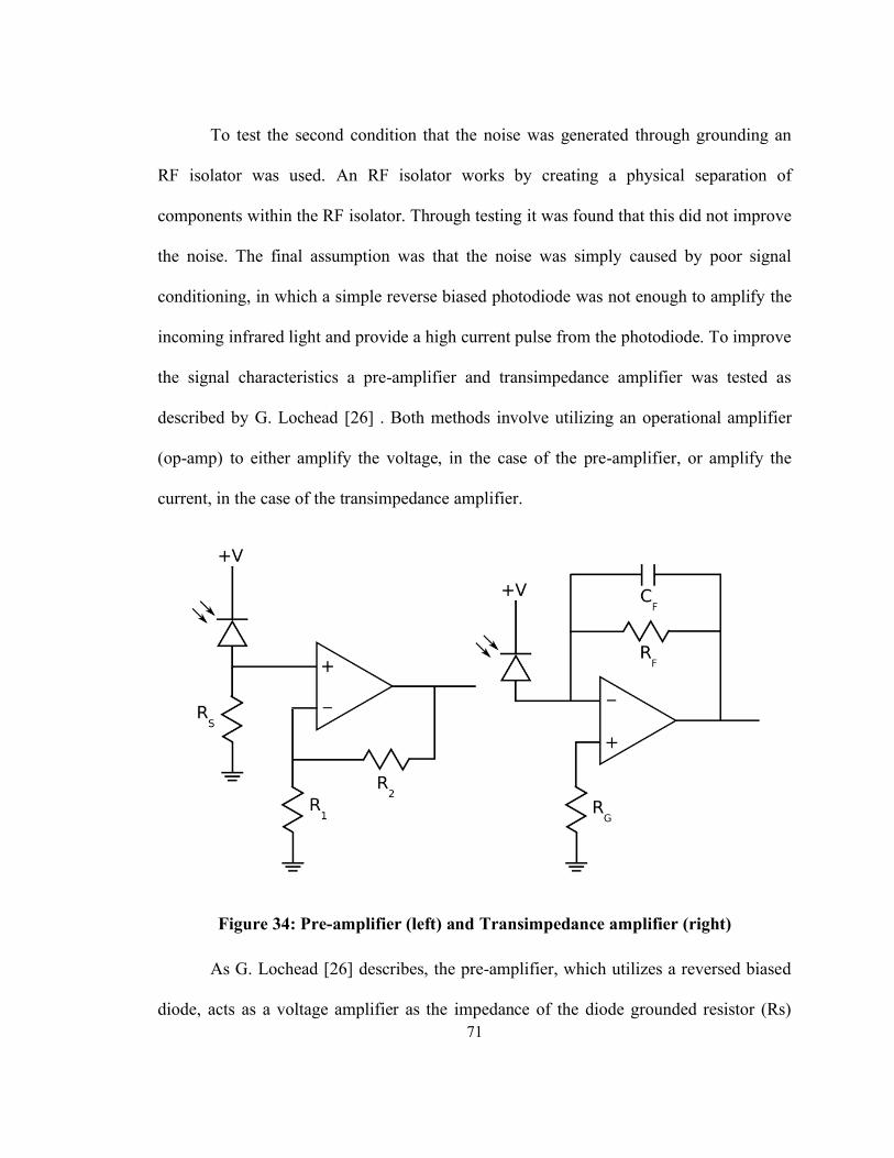
71
To test the second condition that the noise was generated through grounding an
RF isolator was used. An RF isolator works by creating a physical separation of
components within the RF isolator. Through testing it was found that this did not improve
the noise. The final assumption was that the noise was simply caused by poor signal
conditioning, in which a simple reverse biased photodiode was not enough to amplify the
incoming infrared light and provide a high current pulse from the photodiode. To improve
the signal characteristics a pre-amplifier and transimpedance amplifier was tested as
described by G. Lochead [26] . Both methods involve utilizing an operational amplifier
(op-amp) to either amplify the voltage, in the case of the pre-amplifier, or amplify the
current, in the case of the transimpedance amplifier.
Figure 34: Pre-amplifier (left) and Transimpedance amplifier (right)
As G. Lochead [26] describes, the pre-amplifier, which utilizes a reversed biased
diode, acts as a voltage amplifier as the impedance of the diode grounded resistor (Rs)
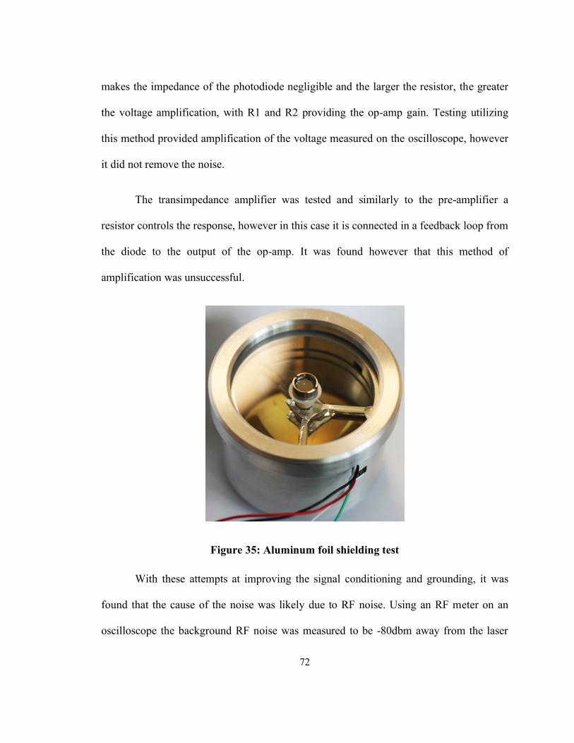
72
makes the impedance of the photodiode negligible and the larger the resistor, the greater
the voltage amplification, with R1 and R2 providing the op-amp gain. Testing utilizing
this method provided amplification of the voltage measured on the oscilloscope, however
it did not remove the noise.
The transimpedance amplifier was tested and similarly to the pre-amplifier a
resistor controls the response, however in this case it is connected in a feedback loop from
the diode to the output of the op-amp. It was found however that this method of
amplification was unsuccessful.
Figure 35: Aluminum foil shielding test
With these attempts at improving the signal conditioning and grounding, it was
found that the cause of the noise was likely due to RF noise. Using an RF meter on an
oscilloscope the background RF noise was measured to be -80dbm away from the laser

73
rangefinder. While the probe was within a range of 0 to 30 millimeters from the laser
rangefinder the oscilloscope reading varied with a maximum of -30 dbm. With proven
evidence of RF interference modifications were made to the laser rangefinder to provide
shielding between the boards through the use of aluminum foil tape, Figure 35, however
this did not reduce the RF impact. In order to further isolate the pulsing and receiving
circuits a new laser rangefinder housing was made that would separate the boards, Figure
36. This however negates the design constraints of overall size. While testing in this
configuration noise was still an issue. Further work needs to be completed in creating
isolation between the devices. This could be completed through mechanical means of
shielding or electrical devices such as opto-isolators. In addition, there may be the
possibility of reviewing the causes of the RF noise emitted from the pulsing circuit and
any options that may be available in the design of the pulsing circuit to minimize this.
Figure 36: Extended housing isolation test

74
Chapter 5: Mechanical Design
5.1. Circuit Board Design
The design for the circuit board was developed based on the minimum required
space to place the electrical components, as well as the minimum area required for
achieving the required light to activate the photodiode. A circular design was chosen as
this maximizes the receiving area with the smallest width. The diameter of the circle was
chosen by adding the area required for the electrical components and support legs of the
suspended center to the required area to receive light transmittance at the design distance
of 1 kilometer for the design optical power as described in 3.6.1. This total area was then
used to find the diameter of the circle.
Three support legs were chosen for the suspended electrical components out of
structural necessity. Using a singular support leg would cause significant potential for
deflection of the electrical components when the laser rangefinder was under any form of
position change, such as the motion of the moving vehicle. Similarly, two support legs
present the potential for rotation of the suspended board, if in a coaxial arrangement, or
deflection as with the singular support leg if the legs were not aligned axially. Using three
support legs provides rigidity of the centrally suspended board. The support legs were
also designed to occupy the minimum amount of area while providing adequate space for
electrical traces to connect the components to the external connectors. By minimizing the
width of the support legs, two are able to be used to carry signal traces, while the third
provides transmission through the ground and power planes to the central board.

75
Two mounting holes were placed on the circuit board in order to provide alignment
within the laser rangefinder housing.
5.2. Housing Design
Using the circuit boards and the optical configuration as the requirements, while
keeping in mind the SWaP considerations, the housing was designed to minimize the
overall size, while creating ease of assembly without over complicating any components
of the device to provide ease of manufacturability. The design criteria for the housing
were defined by the required focal length for the transmission lens, the focal length for
the mirror, spacing between the two circuit boards, and the diameter required to allow
adequate light reception.
Figure 37: Complete Laser Rangefinder Diagram
Housing
Mirror
Alignment Screw
Board Spacer
Receiver and Transmitter Boards
Lens
Connectors
Lens Spacer
Lens Cap
76
A singular body comprises the housing of the laser rangefinder, this will house the
circuit boards, mirror, and combination lens. As the optical design utilizes a collinear
optical axis for transmitting and receiving, it was required to utilize geometric
dimensioning and tolerancing to reduce the chance of error, specifically in the
concentricity of components and placement of the mounting holes which align with the
circuit boards.
The housing is divided into two sections, the optics and circuit section, and the
mirror section. The chosen optical design for the transmission lens consists of a flat plane
lens with an aspherical collimating lens mounted in the center by a fine thread, providing
adjustability for focal length. Therefore, the position of the flat plane lens could be fixed
relative to the circuit boards and the distance between the circuit boards and between the
boards fixed with spacers. Similar to the collimating lens, the mirror required adjustment
for calibration and was therefore isolated in a section of the housing which contained a
fine thread, allowing for the proper focal length to be identified in testing. Additional
requirements for the housing included slots which were machined through the side of the
housing in order to provide access to the connectors on the circuit boards. For the
prototype design a simple connector was used, however, for protection from the
environment, a sealed connector would need to be specified, and adjustment to slot design
would have to be made.

77
Figure 38: Laser Rangefinder Assembly Transparent View of Optical Axis
Figure 39: Laser Rangefinder Assembly Electrical Connections
In addition to the housing, three other parts were required to assemble the laser
rangefinder. To seal the lens into the housing an external lens cap was designed that could

78
thread onto the housing. For the design of the prototype the lens cap directly applies
friction to the lens to hold it in place, however an O-ring face seal could be incorporated
to provide protection from the environment. Two spacers had to be designed for use
within the housing, one between the circuit boards, and another between the transmitting
circuit board and the transmitting lens. The thickness of the spacers did not require a tight
tolerance because of the adjustability built into the lens design, however, to minimize any
movement of components within the interior of the housing a diameter tolerance was
required.

79
Chapter 6: FPGA Design
6.1 Implementation
The FPGA board developed by the INSPIRUS project was used for the testing and
development of the laser rangefinder. The functions of the board can be divided into two
categories, timing and pulse generation and detection.
The pulse generation and detection functions could have been developed utilizing
discrete electronics, however for ease of implementation and maintaining SWaP
requirements these functions were also integrated into the FPGA. The capabilities of the
Altera Cyclone 3 allowed the use of a phase lock loop which can multiply the internal
clock speed of the FPGA. As the clock speed is directly proportional to the accuracy of
distance detection.
The design of the laser range finding system was based around a state machine.
The state machine can exist in a single state at a time, as specified conditions are achieved
the state will change triggering different events. This state machine can be represented by
a loop, where the states continuously cycle through one another. In the “done” state the
program is looking for a trigger signal to begin the laser range finding process. When
initiated the state changes to the “pulse” state in which a trigger is initiated to pulse the
laser. When the pulse is triggered the state will change to the “timing” state in which a
counter is enabled and will count at the phase locked clock speed until a received bit is
identified by the receiver. With the reception of a bit the state will change to the “done”

80
state outputting the count from the counter and await another trigger signal. A state
diagram of the state flow can be found in ____.
Figure 40: State diagram of FPGA Algorithm
6.1.1 Error Checking Algorithm
As there could be a potential for interference creating false positives or loss of
data a signal processing algorithm could be used to ensure that the data received is
accurate. An algorithm is described by Sharma, Visveswaran and Gaba [27] in which a
unique sequence of bits could be transmitted rather than a single pulse. Through the use
of FPGA, this sequence can be stored in a register, the incoming data can then be shifted
through a register at the clock frequency and compared to the original sequence. If a
match is identified it can then be assumed that the correct data has been received as a
successful transmission, stopping the counter. A block diagram in Figure 41 shows the
data flow through this algorithm. The utilization of signal processing will impose an
81
inherent delay on the system as the incoming data is shifted and compared, however this
can be calculated through repeated accurate tests and the delay can be removed from the
timing calculation in order to provide accurate distance information.
Figure 41: Error Checking Algorithm Block Diagram
A sample algorithm was created and realized on an FPGA in which the entire
transmission and reception process would be simulated through the use of a serial
connection with MATLAB. A code was written in MATLAB that would simulate a
desired distance and 8-bit sequence representing the returned signal. This would be
transferred to the FPGA, in which the distance would be represented by a clock lasting for
the desired amount of time provided by MATLAB and once the time was up the 8-bit
sequence was read at the clock speed into a shift register. Using the algorithm provided
by Sharma et al [27], the desired 8 bit sequence is saved in a register and the incoming

82
data is then compared to corresponding bits in each register. In order to initiate the
comparison, the desired sequence must begin with a logic high (1), signaling the most
significant bit of the shift register to trigger the comparison function. Once the successful
comparison was identified and the distance counter stopped, the measured count would be
returned to MATLAB in the form of a distance. This would then be compared to the
provided distance provided and the delay of the system can be identified.

83
Chapter 7: Conclusions
7.1 Successes
The goal of this project was to develop a laser rangefinder that could mount on a
motion platform for aerial sense and avoid applications. In order to achieve this, it would
need to be small in size, lightweight, and consume minimal power.
Through the research and development process it was demonstrated that an
integrated transmitting collimator and receiving lens design can be developed through a
ray tracing algorithm utilizing known input and output characteristics of the optical
transmitter. With minor manipulation, the same principles of this algorithm can be used to
determine the output characteristics for a known lens profile and input transmitter
characteristics.
Success was found in the development of a pulsing circuit that could provide the
required amperage to pulse a laser diode with sufficient optical power for the design
range of 1 kilometer and maintain a minimal surface area to improve light transmission
past the circuit board for the single axis design. The realized circuit performed as
expected based on the simulated model created using MultiSim. Utilizing this circuit with
a FPGA controlling program to provide a pulse trigger the transmission portion of the
project was very promising. The pulsing circuit was able to create a 30 Amp 50
nanosecond pulse at a frequency of 20 Hz with a 12-volt power supply.
In isolated testing the developed receiving circuit was able to detect the infrared
signal from the transmitting pulse, validating the design theory of the receiving circuit.

84
However due to shielding and isolation capabilities the combination of a transmitting and
receiving laser rangefinder was not possible, although each unit worked independently.
The mechanical design of the housing for the rangefinder provided a robust
housing that was capable of minor adjustments to improve the ability to test the device.
The housing design could easily be assembled and was lightweight.
7.2 Review of Expected Outcomes
Outcome 1: An algorithm was developed that was able to produce the lens profile for a
lens capable of collimating light from a laser diode.
Outcome 2: An algorithm was developed that could produce a mirror profile able to focus
ambient light to a known point.
Outcome 3: An experimental evaluation was conducted on the custom designed lens and
mirror. In addition, an experimental evaluation was conducted of a commercial lens to
replace custom lens.
Outcome 4: A pulsing circuit was designed and implemented meeting the design
requirements.
Outcome 5: A receiving circuit was designed and implemented, however it was unable to
perform as desired, not meeting design requirements.
Outcome 6: A controller was developed utilizing an FPGA that could interface with the
laser rangefinder.
Outcome 7: A laser rangefinder housing was designed and manufactured and met the
design requirements.

85
Table 5: Final Laser Rangefinder Specifications
Design Specification Value
Diameter 63.5 mm
Weight 0.177 kg
Repetition Rate 50 Hz
Measurement Range N/A
Accuracy N/A
Power Supply 12V
7.3 Future Work
The theory applied to the lens design and algorithms used imply that it is possible
to manufacture a single lens that will provide the required transmission and receiving
optical parameters required. The limitations that were found due to the machining
processes did not allow for validation of this theory. Possibilities for future testing could
include submission of the design to an outside manufacturer with experience in lens
development to provide more accurate test results and validation of the theory and
algorithm.
The electrical components utilizing in the transmitting and receiving circuits
functioned when isolated from one another, however future development is required to

86
determine the proper amount of shielding required between the transmitting and receiving
electronics to prevent interference, as the two components were successfully tested at a
distance, but caused issues when in close proximity due to RF interference.
The mechanical design of the housing could benefit from improvements around
weather resistance. Additional design elements that would provide increased protection
from the elements such as a face seal on the lens, and O-ring in the lens cap and mirror.
Additional development could be focused around robust connectors, for interfacing the
laser rangefinder with the FPGA board, or an option for integration of the two systems in
one unit.

87
Bibliography
[1] U.S. Army UAS Center of Excellence, “U.S. Army Unmanned Aircraft Systems
Roadmap 2010-2035,” Fort Rucker, Alabama.
[2] Cloud Cap Technology, “TASE150 / TASE200 Compact Lightweight Daylight /
IR Imaging.” Hood River, OR, 2014.
[3] Israel Aerospace Industries LTD, “MicroPOP Micro Pug-in Optronic Stabilized
Payload.” Yehud, Israel, 2008.
[4] Echodyne, “EchoFlight 3D Airborne DAA Radar.” 2020.
[5] G. W. Hamilton, B. Sc, and A. L. Fowler, “The laser rangefinder,” no. September,
1966.
[6] U. S. A. E. Command and F. Monmouth, “Both systems have the disadvantage of
low repetition,” no. 1, 1968.
[7] R. Society, “Mr . Isaac Newton ’ s Considerations upon Part of a Letter of
Monsuur de Berce Printed in the Eight French Memoire , Concerning the Cata-
Drioptrical Telescope , Pretended to be Improv ’ d and Refined by M . Cassegrain
Author ( s ): Isaac Newton and M . Ca,” vol. 7, no. 1672, pp. 4056–4059, 2019.
[8] R. Signals and R. Establishment, “Review Laser rangefinders,” vol. 13, pp. 259–
293, 1981.
[9] Bushnell, “Bushnell Legend Laser Rangefinder Owner’s Guide.” 2019.
[10] Jenoptik, “Unparalleled performance with our second-generation DLEM Laser

88
Rangefinders.” 2019.
[11] R. Paper, “A Review,” vol. 45, no. 4, 1995.
[12] M. The, O. Of, and P. Lasers, “Chapter 11,” 2012.
[13] J. Isoaho and A. Nummela, “Technologies and Utilization of Field Programmable
Gate Arrays.”
[14] Altera, “Altera Phase-Locked Loop (Altera PLL) IP Core User Guide,” 2015.
[15] Sean Higgins, “Laser Scanning: How Does It Work, Anyway? - SPAR 3D,” 2004.
[Online]. Available: https://www.spar3d.com/news/related-new-technologies/laser-
scanning-how-does-it-work-anyway/. [Accessed: 14-Mar-2019].
[16] S. J. Alonso, M. Rubio, F. Martín, and G. Fernández, “COMPARING TIME-OF-
FLIGHT AND PHASE-SHIFT . THE SURVEY OF THE ROYAL PANTHEON
IN THE BASILICA OF SAN ISIDORO ( LEÓN ),” vol. XXXVIII, no. March, pp.
2–4, 2011.
[17] R. Kingslake and R. B. Johnson, Meridional Ray Tracing, Second. Burlington,
MA: Academic Press, 2010.
[18] S. N. Kasarova, N. G. Sultanova, C. D. Ivanov, and I. D. Nikolov, “Analysis of the
dispersion of optical plastic materials,” Opt. Mater. (Amst)., vol. 29, no. 11, pp.
1481–1490, Jul. 2007.
[19] S. M. Nejad and S. Olyaee, “Low-Noise High-Accuracy TOF Laser Range
Finder,” Am. J. Appl. Sci., vol. 5, no. 7, pp. 755–762, 2008.

89
[20] J. Wojtanowski, M. Zygmunt, M. Kaszczuk, Z. Mierczyk, and M. Muzal,
“Comparison of 905 nm and 1550 nm semiconductor laser rangefinders ’
performance deterioration due to adverse,” vol. 22, no. 3, pp. 183–190, 2014.
[21] O. Loebich, “The Optical Properties of Gold,” Gold Bull., vol. 5, no. 1, pp. 2–10,
1972.
[22] Q. Wang, X. Tian, G. Wu, and M. Luo, “Design of high-peak current and narrow
pulse driver of laser diode,” J. China Univ. Posts Telecommun., vol. 16, no.
September, pp. 82–85, Sep. 2009.
[23] W. Reeb and L. C. Gmbh, “Drive Electronics for Pulsed Laser Diodes Power
where it Matters.”
[24] National Instruments, “NI Circuit Design Suite.” Austin, Texas, 2012.
[25] Panasonic, PIN Photodiode for Optical Fiber Communication Systems. 2013.
[26] G. Lochead, “Photodiode amplifiers Pre-amplifier,” pp. 1–8.
[27] P. Sharma, G. S. Visveswaran, and S. P. Gaba, “Digital Signal Processing using
Barker Code for Application in Laser Range Finder,” vol. 28, pp. 90–95, 2012.

90
Appendix A: Mechanical Drawings

91

92

93
94

95
96