development of a nano manipulator based on an atomic force
TRANSCRIPT

Arch Histol Cytol, 72 (4/5): 271-278 (2009)
Received March 28, 2009
*This work was supported in part by a leading project of the Ministry of Education, Sports, Science and Technology, "Development of elementary techniques for the electron microscope in the next generation" (to FI and TU), and by a Grant-in-Aid for Sientific Research from Japan Society for the Promotion of Science (to TU).
Address for correspondence: Dr. Futoshi Iwata, Department of Mechanical Engineering, Facul ty of Engineering, Shizuoka University, Hamamatsu, 432-8561, JapanTel & Fax: +81-53-478-1072E-mail address: [email protected]
Development of a nano manipulator based on an atomic force microscope coupled with a haptic device: a novel manipulation tool for scanning electron microscopy*
Futoshi Iwata1, Shinsuke Kawanishi1, Hisayuki Aoyama2, and Tatsuo Ushiki3
1Department of Mechanical Engineering, Faculty of Engineering, Shizuoka University, Hamamatsu; and 2Department of Mechanical Engineering and Intelligent Systems, University of Electro-Communications, Chofu; and 3Division of Microscopic Anatomy and Bio-imaging, Department of Cellular Function, Niigata University, Graduate School of Medical and Dental Sciences, Niigata, Japan
since the operator can move the AFM probe freely at any position on the sample surface while feeling the interaction force between the probe and the sample surface. We tested two types of cutting methods: simple cutting and vibration cutting. Our results showed that vibration cutting with probe oscillation is very useful for the dissection of biological samples which were dried for SEM observation. Thus, cultivated HeLa cells were successfully micro-dissected by vibration cutting, and the dissection process could be observed in real time in the SEM. This AFM manipulation system is expected to serve as a powerful tool for dissecting various biological samples at the micro and nanometer-scale under SEM observation.
Introduction
Scanning probe microscopes (SPMs) are a family of microscopes which scan a probing tip over the sample surface. SPMs have been mainly used as surface imaging tools with nanometer scale resolution, but they can be also used for local surface manipulation. Manipulators based on SPMs are expected to become powerful tools not only for material science but also for biology because micrometer and nanometer scale objects can be moved or fabricated in various (i.e, vacuum, air or liquid) conditions by them. Indeed, several studies involving manipulation have been performed by SPMs (Decossas et al., 2003; Yongda et al., 2007). However, as for such nanometer scale manipulation using conventional SPMs, the manipulation itself cannot be viewed during the operation. The operator therefore has to move the probe in a blind condition, which often induces damage to the
Summary. We developed a novel nano manipulator based on an atomic force microscope (AFM) that can be operated inside the sample chamber of a scanning electron microscope (SEM). This AFM manipulator is also coupled with a haptic device, and the nanometer-scale movement of the AFM cantilever can be scaled up to the millimeter-scale movement of the pen handle of the haptic device. Using this AFM manipulation system, we were able to observe the AFM cantilever and samples under the SEM and obtain topographical images of the AFM under the SEM. These AFM images contained quantitative height information of the sample that is difficult to obtain from SEM images. Our system was also useful for positioning the cantilever for accurate AFM manipulation because the manipulation scene could be directly observed in real time by SEM. Coupling of the AFM manipulator with the haptic device was also useful for manipulation in the SEM
272 F. Iwata et al.:
scale manipulation and fabrication, not only for material sciences but also in biological fields. We recently developed a nanometer-scale manipulator based on an AFM coupled with a haptic device that can be operated under the SEM. Using this system, operators can monitor the manipulation by SEM not only visually but also tactilely by the haptic device in real time conditions. In the present paper, we introduce the details of this system and show its applicability to the manipulation of biological samples under SEM observation.
Material and Methods
Compact AFM manipulator
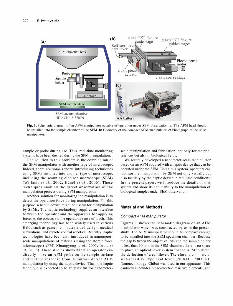
Figures 1 shows the schematic diagram of an AFM manipulator which was constructed by us in the present study. The AFM manipulator should be compact enough to be installed into the SEM specimen chamber. Because the gap between the objective lens and the sample holder is less than 10 mm in the SEM chamber, there is no space to place an optical lever system for the AFM to detect the deflection of a cantilever. Therefore, a commercial self-sensit ive type canti lever (NPX1CTP003, SII Nanotechnology, Chiba) was used in our apparatus. This cantilever includes piezo-electric resistive elements, and
sample or probe during use. Thus, real-time monitoring systems have been desired during the SPM manipulation. One solution to this problem is the combination of the SPM manipulator with another type of microscope. Indeed, there are some reports introducing techniques using SPMs installed into another type of microscope, including the scanning electron microscope (SEM) (Willams et al . , 2002; Hänel et al . , 2006). These techniques enabled the direct observat ion of the manipulation process during SPM manipulation. Another solution for monitoring the manipulation is to detect the operation force during manipulation. For this purpose, a haptic device might be useful for manipulation by SPMs. The haptic technology supplies an interface between the operator and the apparatus for applying forces to the objects via the operator's sense of touch. This emerging technology has been widely used in various fields such as games, computer-aided design, medical simulations, and remote control robotics. Recently, haptic technologies have been also introduced in nanometer-scale manipulations of materials using the atomic force microscope (AFM) (Guangyong et al., 2005; Iwata et al., 2008). These studies showed that an operator can directly move an AFM probe on the sample surface and feel the response from its surface during AFM manipulation by using the haptic device. Thus, the haptic technique is expected to be very useful for nanometer-
Fig. 1. Schematic diagram of an AFM manipulator capable of operation under SEM observation. a: The AFM head should be installed into the sample chamber of the SEM. b: Geometry of the compact AFM manipulator. c: Photograph of the AFM manipulator.

Manipulation tool for SEM 273
piezoelectric actuator. As for the z axis, an external elliptical shell (APA-60S, CEDRAT Technologies, France) including a piezoelectric actuator was used; this also mechanically amplifies the stroke of the piezoelectric actuator three times. The maximum strokes of the x, y and z axis scanners are 50, 50 and 60 μm, respectively.
Coupling with a haptic device
Figure 2a shows a schematic diagram of the manipulation sys tem. The en t i re sys tem cons is t s o f the AFM manipulator, a controller, a PZT driver, a haptic device and a personal computer (PC). The compact and stand-alone AFM manipulator was put on the sample stage in the SEM chamber (S-3700N, Hitachi, Tokyo). We employed a commercial haptic device that has a pen-like handle with a serial rink mechanism
the deflection of the cantilever can be directly detected as an electric signal without any optical lever systems. Thus, the insertion of the self-detective cantilever under the objective lens of the SEM allowed us to design a compact AFM manipulator for operation under SEM observation. The AFM manipulator is a stand-alone type AFM, which has a z axial coarse positioning stage and x, y, z axial fine positioning mechanism. For the z axial coarse positioning, a small z axial stage was assembled with a miniature piezoelectric motor (Picomotor, New Focus Technologies, USA). For the fine positioning and scanning mechanism, a large stroke movement is required for the manipulation of biological samples. In order to achieve a large scanning range, flexure guide stages consisting of a parallel spring structure and a piezoelectric actuator were constructed for each axis in the x and y direction which mechanically triples the stroke of the
Fig. 2. a: Schematic diagram of the experimental setup of the AFM manipulator. The AFM is coupled with a haptic device, so the operator feels the response from the sample during scratching. b: Photograph of the manipulator system.

274 F. Iwata et al.:
signal is sent to the feedback controller to change the setting point of the feedback control. The system then changes the force between the probe and the surface in response to pushing by the operator. Through this sequential process, the operator can change the applied force for the manipulation or fabrication of the sample while feeling the response from the sample surface via the haptic device.
FIB cut cantilever for nano manipulation
In order to perform an accurate manipulation, the probing tip of the AFM manipulator should be directly observed under the SEM. However, the probe of the commercial cantilever is not observed in the top view image ( because the probe is present on the lower side of the cantilever (Fig. 3a, b). In order to solve this problem, the end of the cantilever was partly cut by using focused ion beam milling (Fig. 3c, d). This enabled the probing tip to be recognized in the top view SEM image as shown in Fig. 3d, which allows us to access the probe precisely and accurately to the target position on the sample surface.
(PHANTOM desktop; SensAble Technologies, USA) (Fig. 2b). An operator can move the AFM cantilever directly on the sample while feeling the response from the sample surface. The homemade controller and software were modified to include the haptic device for the manipulation. With respect to the lateral movement in the x and y directions, a signal from the haptic device is sent to the personal computer, and the signal is sent to the piezo drive circuit by passing through a digital-to-analog converter. The topographical signal detected in the AFM controller is fed to the personal computer, and the signal is converted to the displacement in the z-direction of the pen handle of the haptic device. Using this process, the nanometer-scale movement of the cantilever detected by the AFM can be scaled up to the millimeter-scale movement of the pen handle of the haptic device. As a result, the nanometer-scale topography on the sample surface can be felt with operator's fingers through the pen handle. Thus, using this technique, the operator can move the AFM cantilever on the sample surface to any position and feel the response from the sample surface through the cantilever deflection. During the manipulation, if the operator pushes the pen handle against the response, a signal is sent to the personal computer to calculate and convert the force feedback signal, and the converted
Fig. 3. Fabrication of the cantilever for improving operationality under SEM observation a: Original shape of the commercial cantilever. b: Top view image of the cantilever. The probing tip is hidden by the body of the cantilever. c: Cantilever fabricated by FIB cutting. The end of the cantilever was milled by taper cutting. d: Top view image of the fabricated cantilever. The edge of the probe is easily recognized.

Manipulation tool for SEM 275
it was easy to recognize the probing tip of the FIB fabricated cantilever. After we decided on an area to be studied, we could move and approach the cantilever for AFM imaging in the SEM. In this operation, the probe was easily positioned at the area for AFM imaging, and then scanning could be carried out in a contact mode under the SEM observation. The sequential operation was very smooth and convenient for AFM observation, and, during the AFM operation under SEM observation, there was no cross-talk and no electrical-noise between both the SEM and the AFM systems. Thus, we were able to obtain the topographical image of AFM under SEM observation (Fig. 4b). In Figure 4, the AFM image of the HeLa cell (b) exactly corresponds to the square region of the SEM image (a). This enabled details of the surface topography of the cell with height information to be distinguished in the AFM image.
Dissection of HeLa cells under SEM observation
To verify the performance of our manipulation system, we dissected HeLa cells with the AFM manipulator under SEM observation. The haptic device used in our system enabled the dissection of HeLa cells with the AFM probe, as if we could directly feel the loading force of the cantilever with the operator's hand. When the cells were cut by a simple movement of the AFM probe with the average loading force of 10 μN, the cut line was not smooth but irregular, as shown in Figure 5a. During the process, we also felt any irregularity in the dissecting
Sample preparation
In this experiment, HeLa cells were used in the present study. They were grown on glass coverslips according the standard procedure of the cell culture. Briefly, the cells were cultivated on the coverslip in a culture medium (RPMI 1640, Invitrogen Japan, Tokyo) containing 10% fetal bovine serum and antibiotics, at 37℃ in a 5% CO2 incubator for 1–3 days. The cells on the coverslip were fixed with 1.5% glutaraldehyde in a 0.1% phosphate buffer (pH 7.4) for 2 h or more and then conductive-stained by treatment with a 0.5% tannic acid solution and a 1% osmium tetoxide solution. They were dehydrated in a series of ethanol, transferred to isoamyl acetate and dried in a critical point dryer using liquid CO2. The coverslips with dried cells were mounted on aluminum stubs with double-sided adhesive carbon tape and coated with platinum-palladium in an ion coater for SEM observation.
Results
AFM imaging under SEM observation
Using our AFM manipulation system, we were able to observe the cantilever and samples by SEM, while operating the cantilever for the AFM imaging of samples. Figure 4a shows an SEM image of HeLa cells and the manipulating cantilever. As shown in this micrograph,
Fig. 4. AFM imaging of a HeLa cell under SEM observation. a: SEM image of HeLa cells and the cantilever. The square is a scanning area for AFM imaging. b: AFM topographical image of the HeLa cell.

276 F. Iwata et al.:
response with our fingers via the haptic device. This is probably because dried biological samples are not uniform but rather fragile in structure, which resulted in a cracking or collapsing of the sample surface as if the samples had been scratched with a blunt needle. To cut the HeLa cells smoothly and effectively, we then carried out vibration cutting with probe oscillation. A modulation signal of 9 kHz with an amplitude of 50 nm was added to the y axis scanner. Figure 5b shows the scratched lines from cutting with probe vibration. The direction of the probe vibration was parallel to the long axis of the cantilever. The average loading force was 2μN. Using this method, the cells were successfully dissected with a smooth cutting line. The cutting edge was sharp and there was no surface distortion in the periphery of the cutting region; even the loading force was lower than in the case of cutting without a probe
vibration. Figure 5c shows scratched lines by cutting with and without probe vibration. In both cases, the average loading force was 2μN. As described above, the cell process was successfully dissected with vibration cutting and the cutting line was smooth and sharp. On the other hand, the cell process was not cut but slightly scratched when the probe was not vibrated during cutting. Thus, the vibration cutting was very effective for the dissection of dried biological samples in the SEM. Figure 5d shows an example of cell dissection by vibration cutting: the letter "S" was carved on the surface of the HeLa cell by vibration cutting with the haptic device. The average loading force was 2μN. During the process, we were able to carve the surface while sensing a smooth response in the haptic device.
Fig. 5. SEM images of HeLa cells cut by the AFM manipulator using the haptic device. a: Fabrication by cutting without probe vibration. The broken line indicates the trajectory of the probe. It is difficult to cut the cell smoothly. b: Fabrication by cutting with probe vibration. The HeLa cell was successfully dissected. c: Cutting of the cell process with and without probe vibration. In both cases, the same loading force of 2μN was applied. d: Carving a letter "S, on the surface of the HeLa cell.

Manipulation tool for SEM 277
Discussion
The present study has introduced a compact AFM which can operate in the sample chamber of the SEM, demonstrating its applicability to the biological fields not only as an imaging tool but also as a novel manipulation tool for SEM. SEM has been widely used for obtaining three-dimensional information of samples at the millimeter to nanometer scales. However, there is no quantitative height information in conventional SEM images. For instance, the edge line of the HeLa cell is bright in the SEM image due to the edge effect produced by secondary electrons, even though the actual height of this part is topographically low. On the other hand, AFM images contain quantitative information in three dimensions, and the sample profile containing height information can be easily obtained. Therefore, by coupling SEM with AFM, it becomes possible to analyze the sample height from AFM imaging while observing the detail of the surface topography by SEM. In addition, the combination of AFM and SEM is useful for AFM imaging because the probing tip of the cantilever can be easily and accurately approximated to the sample of interest under SEM observation. Our system is expected to become a powerful tool for obtaining AFM images of the restricted regions of bulky samples because the accurate approach of the AFM probe to the bulky samples is very difficult under optical microscopic observation. In the present study, we also demonstrated that our AFM system is useful for the manipulation of samples under the SEM. We especially showed that the haptic device is effective for AFM manipulation because the operator can move the AFM probe rather freely to any position on the surface while feeling the interaction force detected by the cantilever on the sample surface. As for the cutting performance of our system, we tested two type of cutting methods: simple cutting and vibration cutting. Our results showed that the vibration cutting with probe oscillation is very useful for the dissection of biological samples prepared and dried for SEM observation. We previously used the vibration cutting method for dissecting different samples including the soft polymers and dried collagen fibrils (Iwata et al., 1999, 2008). These previous studies also revealed the usefulness of vibration cutting for dissecting both hard samples and elastic soft samples. In the present study, we also showed how vibration cutting is further useful for the dissection of dried, fragile biological samples. On the other hand, simple cutting without probe oscillation is not suitable for the precise dissection of our samples, probably because
it produces a sliding interaction between a probe of the AFM and the sample surface (Meyers et al., 1992; Leung and Goh, 1992), making it difficult to cut the sample smoothly for micro or nanometer-scale fabrication. For dissecting samples in an SEM, sensing the distance between the AFM probe and the sample is very important to avoid any bumping of the probe onto the sample. Although the SEM provides three-dimensional images, a single micrograph from conventional SEM presents a view for only one eye, and it is difficult to realize correctly the depth of the observation field. Thus, an SEM with real-time stereo imaging by the simultaneous collection of stereo-pair images would be useful for manipulation in an SEM. We are now interested in the manipulation in this type of SEM, and the details will be described later in a separate paper. In conclusion, we developed a novel nano manipulator based on an AFM which can be operated inside the sample chamber of the SEM. This system enabled us to observe the manipulation in real time observations by using the SEM. Through the coupling of the AFM manipulator with a haptic device for human interface, the operator can move the AFM probe to any position on the surface while feeling the loading force against the sample with the his/her hand. This system is expected to become a powerful tool for dissecting biological samples at various micro and nanometer-scales under SEM observation.
AcknowledgementsWe thank the designers of Hitachi High-Technologies Corporation for providing the SEM system.
References
Decossas S, Patrone L, Bonnot AM, Comim F, Decossas M, Baraski A, Chevrier J: Nanomanipulation by atomic force microscopy of carbon nanotubes on a nanostructured surface. Surf Sci 543: 57-62 (2003).
Guangyong L, Ning X, and Donna HW: In situ sensing and manipulation of molecules in biological samples using a nanorobotic system. Nanomedicine 1: 31-40 (2005).
Hänel K, Brinkner A, Müllegger S. Winkler A, Wòll C: Manipulation of organic needles using an STM operated under SEM control. Surf Sci 600: 2411-2416 (2006).
278 F. Iwata et al.
Iwata F, Matsumoto T, Ogawa R, Sasaki A: Scratching on polystyrene thin film without bumps using atomic force microscopy. J Vac Sci Technol B17: 2452-2456 (1999).
Iwata F, Ohara K, Ishizu Y, Sasaki A, Aoyama H, Ushiki T: Nanometer-scale manipulation and ultrasonic cutting using an atomic force microscope controlled by a haptic device as a human interface. Jpn J Appl Phys 47: 6181-6185 (2008).
Leung OM, Goh MC: Orientation ordering of polymers by atomic force microscope tip-surface interaction. Science 3: 64-66 (1992).
Meyers GF, DeKoven BM, Seitz JT: Is the molecular surface of polystyrene really glassy. Langmuir 8: 2330-2335 (1992).
Willams PA, Patel AM, Sinclair M, Seeger A, Helser A: Controlled placement of an individual carbon nanotube onto a microelectromechanical structure. Appl Phys Lett 80: 2574 - 2576 (2002).
Yongda Y, Tao S, Yingchun L, Shen D: Investigation on AFM-based micro/ nano-CNC machining system. Int J Machine Tool Manuf 47: 1654-1659 (2007).