development of 200mips-class 64bitmpu for space application · development of 200mips-class...
TRANSCRIPT

1
Development of 200MIPS-class 64bitMPU for Space Application
“Development of 64bit MPU for highly functional space system of the next generation, by adopting COT and HBD”
October 22nd 2004High-Reliability Components Corporation

2
The purpose of the development
• High performance MPU is recognized as “strategic parts” and required to develop (by Japanese original technology) for high performance oriented satellite.
• It should be required that the satellite components which can calculate the huge data will be developed.
• It’s difficult to obtain the high performance MPU for space application, which is essential to satellite on-board computer.

3
The details of the developmentFy2002 Fy2003
Development and test of radiation hardening cells SEL Test
SEU Test
SET Test
Preparation of cell library
200MIPS class 64bit MPUSpecification・Design
Manufacture of Pre Production device
Designing for 304pin PKG
Development of ICE
Development of evaluation board
Test of device
Pre Qualification Test(QT),
Manufacture for QT device
Higher function
Manufacture of pre Production device using HBD cell
Development of RTOS
Designing for 304pin PKG
Test of device
1st. trial production
2nd. trial production
Fy2004

4
Requirement for MPU• Investigated the user requirement in the user’s
meeting by JAXA, and reached the followingdecision– MPU core and peripheral circuit within 1chip– MPU core
• MIPS 5KfTM 64bitMPU 32kbytes instruction & data cache memory
64bits Floating-point unit• 200MHz operate
– Peripheral circuit• Memory Controller(8bank,8bit/16bit/32bit/64bit)• DMA Controller(2channels)• UART(Functionally compatible with 16550, 2channels)• Timer/Counter(2channels)• Interrupt controller • PCI controller (66MHz,32bits,PCI spec. 2.2)

5
COT ProcedureUsing radiation hardening cells, Creating GDSⅡCircuit design
Multiple use of applicable designs
Manufacture Mask
Manufacture Wafer Commercial foundry line
Wafer banking
Assembly
Screening
Optimization of Qualification Test
Use of in-process inspection
GroupA(Electrical test)
GroupB (workmanship)
GroupC(life)
GroupD(pakage)
Periodical evaluation by typical sample
Qualification Test

6
1st. Trial Production• Development Flow
Specifications examination
Provide peripheral circuit
Front-End design
Back-End design
Manufacture of Wafer
Assembly
Package design LSI tester program
Tests

7
1st. Trial Production• Provide peripheral circuit
– Procurement conditions• Have the MIPS 5KfTM interface(EC interface) and be able to
interface with peripheral circuit• Possible to provide all peripheral IPs (Have a miss interface when made by several manufacturers)
• Possible to customize IPs• Possible to make new IPs
Select a design house to meet with the above conditions

8
1st. Trial Production– Specifications of peripheral circuit
The peripheral circuit block diagram.
UART CPU Bus Slave
Memory Controller
Interrupt Controller
PCI Bus Arbiter
Control Register
PCI Host Bridge
DMA
Timer
PCI Bus
CPU Bus
UART CPU Bus Slave
Memory Controller
Interrupt Controller
PCI Bus Arbiter
Control Register
PCI Host Bridge
DMA
Timer
PCI Bus
CPU Bus

9
1st. Trial Production• Front-End/Back-End design
– Design language : Verilog-HDL– PLL is used in each of core,
peripheral and PCI– Possible to select each
frequency in core, peripheral and PCI
– Cache memory including parity with MBU(Multi-Bit-Upset) protection
5mm
10mm

10
1st. Trial Production• Development of 304pin ceramic QFP-Package
– Same size with 1MG/A, and compatibility of IC socket and career
– Change the cavity size(chip size 5×10mm□)– 2 power supplies that different
from 1MG/A (1.8V/3.3V)
– Radiation shielded for TID

11
1st. Trial Production
ICEICE
200200MIPS MPUMIPS MPU
Test BoardTest Board
ICEICE
200200MIPS MPUMIPS MPU
Test BoardTest Board
• Verification(Test)
– Using LSI tester for MPU
– Prepare a development environment for MPU .(photo)
• ICE:Provide AdvicePlus by YDC• Development of evaluation board for
MPU
– Verification by software for MPU
12
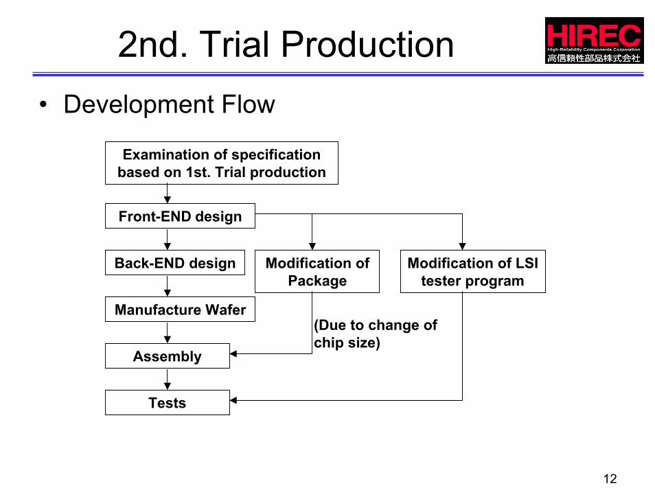
2nd. Trial Production• Development Flow
Examination of specification based on 1st. Trial production
Front-END design
Back-END design
Manufacture Wafer
Assembly
Modification of Package
Modification of LSI tester program
(Due to change of chip size)
Tests

13
2nd. Trial Production• Examination of specification based on 1st.
Trial production– Procedures to avoid design mistake
• Shortage of operational speed margin in peripheral circuit• Misconnection between PCI and test clock• Discrepancy between actual function and specification of
peripheral circuit
– Modification to improve performance and usability• Higher speed of parity circuit in the cache memory• Addition of 4:1 operation speed between MPU and peripheral
circuit• Optimization of PLL circuit• Reduction of switching noise by improvement of power
supplies and GND.

14
2nd. Trial Production• Mitigation agaist SEEs
– HBD(Hardness-By-Design) is:• The method to mitigation against the radiation effects by
implementing circuit design utilizing the pure commercial process
– Design of several FF/Latch by HBD methodology• Mitigation against SEU/SET• Cell area:approx 2 times(following figuers:patent pending)
• Propagation delay:no increase• Power:approx 2 times
Original standard cell(Latch)Original standard cell(Latch) HBD cell(Latch)HBD cell(Latch)

15
2nd. Trial Production• Front-End/Back-End design
– Usage of the HBD cell library• Applicable for all FF/Latch• 7×10mm□ total chip area
– Cache memory including parity with MBU protection
– Improvement of power supplies and GND
– Optimization of the PLL circuit
7mm
10mm

16
2nd. Trial Production• Modification of 304 pin ceramic QFP Package
– Modified the cavity size due to the change of chip sizeto (5×10mm□ →7×10mm□)
– Radiation shielded for TID

17
2nd. Trial Production• Verification(Test)
– Verification of MPU by LSI tester– Use of RTOS(Real-Time-OS)– eSOL:eBinder(μITRON)
• Performed operational verification by preparing operational program which can net be verified by IEC alone

18
2nd. Trial Production• Measurement of Power consumption
– Conditions:• Under continuous cache access operations• Ratio of operational frequency core:peripheral = 2:1
0.00
0.50
1.00
1.50
2.00
2.50
3.00
3.50
4.00
4.50
5.00
0 50 100 150 200 250
周波数[MHz]
消費
電力
[W]
85℃ 1.95V/3.6V
25℃ 1.95V/3.6V
85℃ 1.8V/3.3V
25℃ 1.8V/3.3V

19
Radiation Hardness• Radiation Immunity of MPU
– Test results of SEU for basic circuits in MPU
Circuit name SRAM-PW SRAM-HS RH-Latch PLL-8211 PLL-8511Number of use in MPU 594944 73728 34551 1 1
Cross Section [cm2/bit] 3.16E-07 3.28E-07 <1.05E-9 4.88E-07 4.36E-07
LETth [MeV/(mg/cm2)] 0.46 0.46 >40.3 >6.54 >3.56
Solar Min. [SEUs/bit/day] 2.28E-07 2.33E-07 1.24E-15 5.70E-07 1.96E-06[SEUs/device/day] 1.36E-01 1.72E-02 4.28E-11 5.70E-07 1.96E-06
Solar Max. [SEUs/bit/day] 9.54E-08 9.77E-08 2.76E-16 1.32E-07 7.76E-07[SEUs/device/day] 5.68E-02 7.20E-03 9.54E-12 1.32E-07 7.76E-07
Solar Min. [SEUs/bit/day] 6.66E-07 6.80E-07 3.68E-15 2.00E-06 5.88E-06[SEUs/device/day] 3.96E-01 5.01E-02 1.27E-10 2.00E-06 5.88E-06
Solar Max. [SEUs/bit/day] 2.36E-07 2.41E-07 8.26E-16 6.80E-07 1.89E-06[SEUs/device/day] 1.40E-01 1.78E-02 2.85E-11 6.80E-07 1.89E-06
** ALOS orbit : height 692km, inclination 98.16°, stormy
geosynchronous orbit : height 36000km, inclination 0°, stormy
Predicted SEU rate (ALOS orbit)
Predicted SEU rate (geosynchronous orbit)

20
Radiation Hardness• Radiation Immunity of MPU
– Test results of proton SEU for SRAM circuits in MPU
Circuit name SRAM-PW SRAM-HSNumber of use in MPU 594944 73728
A (fitting parameter)* 0.083
B (fitting parameter)* 0.066
Solar Min. [SEUs/bit/day] 3.80E-07 2.46E-07[SEUs/device/day] 2.26E-01 1.81E-02
Solar Max. [SEUs/bit/day] 2.51E-07 1.62E-07[SEUs/device/day] 1.49E-01 1.19E-02
Solar Min. [SEUs/bit/day] 2.38E-08 1.54E-08[SEUs/device/day] 1.42E-02 1.14E-03
Solar Max. [SEUs/bit/day] 8.50E-09 5.49E-09[SEUs/device/day] 5.06E-03 4.05E-04
* fitting parameter of Bendel 2 parameter fitting** ALOS orbit : height 692km, inclination 98.16°, stormy geosynchronous orbit : height 36000km, inclination 0°, stormy
Weibull fitting
Predicted SEU rate (ALOS orbit)**
Predicted SEU rate (geosynchronous orbit)**

21
Radiation Hardness• Radiation Immunity of MPU
– The prediction of SEU for SRAM circuits in MPU(heavy ion, Proton)
Circuit name SRAM-PW SRAM-HS
Solar Min. [SEUs/device/day] 3.62E-01 3.53E-02Solar Max. [SEUs/device/day] 2.06E-01 1.91E-02
Solar Min. [SEUs/device/day] 4.10E-01 5.13E-02Solar Max. [SEUs/device/day] 1.45E-01 1.82E-02** ALOS orbit : height 692km, inclination 98.16°, stormy geosynchronous orbit : height 36000km, inclination 0°, stormy
Predicted SEU rate (ALOS orbit)**
Predicted SEU rate (geosynchronous orbit)**
Number of use in MPU 594944 73728
• SEL immunity : 64[MeV/(mg/cm2)• TID immunity : 1kGy(Si)

22
Development Result Up To Now
• Specification of 200MIPS class 64bitMPU– Developed MPU integrating 32kB instruction cache &
32kB data cache, 64 bit Floating-point unit(FPU) Processor
– Integrated the following peripheral circuits• Memory Controller(8bank,8bit/16bit/32bit/64bit)• DMA Controller(2channels)• UART(Functionally compatible with 16550, 2channels)• Timer/Counter(2channels)• Interrupt controller • PCI controller (66MHz,32bits,PCI spec. 2.2)
– Integrated MIPS 5KfTM and peripheral circuit in one chip

23
Development Result Up To Now
• Functional evaluation of trial sample and arrangement of development support tools
– Performed functional evaluation of MIPS 5KfTM and peripheral circuits, by using trial sample, and confirmed that the essential functions intgrated in MPU are working satisfactorily
– Arranged development support tools including LSI tester, ICE and RTOS, during the course of functional evaluation
– Realized operational speed of 200MHz in MPU core, while 100MHz in peripheral

24
Plan from now on• FY2004,1st. Half(Now):
– Passed preparatory verification tests for MPU developed, satisfactory
– Under 2nd trial MPU production• FY2004, 2nd Half:
– Will perform development verification test• FY2005:
– Production of Flight Model