develop of arm mbed os support for bluenrg-2, a soc
TRANSCRIPT

Collegio di Ingegneria Elettronica, delle Telecomunicazioni e Fisica
Corso di Laurea Magistrale in Ingegneria Elettronica
Tesi di Laurea Magistrale
Develop of ARMMbed OS support forBlueNRG-2, a SoC capable to run applications
based on Bluetooth Low Energy protocol.
Relatore:Chiar.mo Prof. Maurizio MARTINACorrelatore:Chiar.mo Ing. Antonio VILEI
Candidato:
Antonio ORLANDO - 231012
Marzo-Aprile 2019


Contents
Introduction 1
1 Bluetooth Low Energy Architecture 5
1.1 Basic Rate (BR) vs Bluetooth Low Energy (LE) . . . . . . . . . . . . . . . . . . 6
1.1.1 LE Network Topologies . . . . . . . . . . . . . . . . . . . . . . . . . . 9
1.2 LE Protocol Stack . . . . . . . . . . . . . . . . . . . . . . . . . . . . . . . . . . 12
2 Bluetooth Low Energy Stack Design and Organization 17
2.1 PHY - Physical Layer . . . . . . . . . . . . . . . . . . . . . . . . . . . . . . . . 17
2.2 LL - Link Layer . . . . . . . . . . . . . . . . . . . . . . . . . . . . . . . . . . . 20
2.3 HCI - Host Controller Interface . . . . . . . . . . . . . . . . . . . . . . . . . . 22
2.3.1 HCI packet standard . . . . . . . . . . . . . . . . . . . . . . . . . . . . 25
2.4 L2CAP - Logical Link Control and Adaption Protocol . . . . . . . . . . . . . . 28
2.5 SM - Security Manager . . . . . . . . . . . . . . . . . . . . . . . . . . . . . . . 29
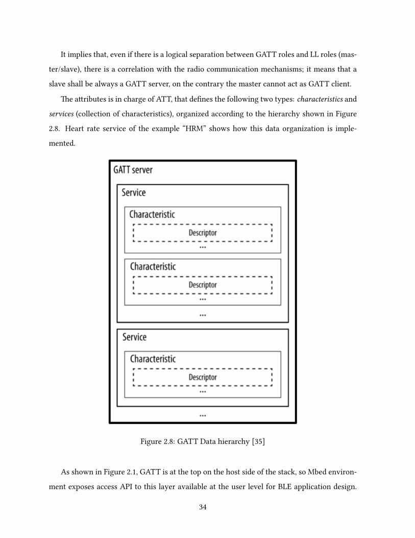
2.6 ATT - A�ribute Protocol . . . . . . . . . . . . . . . . . . . . . . . . . . . . . . 32
2.7 GATT - Generic A�ribute Pro�le . . . . . . . . . . . . . . . . . . . . . . . . . 33
2.8 GAP - Generic Access Pro�le . . . . . . . . . . . . . . . . . . . . . . . . . . . . 35
2.8.1 GAP Modes . . . . . . . . . . . . . . . . . . . . . . . . . . . . . . . . . 37
2.8.2 GAP Procedures . . . . . . . . . . . . . . . . . . . . . . . . . . . . . . 37
3 BlueNRG-2 STMicroelectronics System-On-Chip 39
3.1 ARM Cortex-M0 Core Architecture . . . . . . . . . . . . . . . . . . . . . . . . 41
3.2 Peripherals . . . . . . . . . . . . . . . . . . . . . . . . . . . . . . . . . . . . . . 44
i

3.2.1 GPIO . . . . . . . . . . . . . . . . . . . . . . . . . . . . . . . . . . . . . 44
3.2.2 Wake up Controller and Reset . . . . . . . . . . . . . . . . . . . . . . . 47
3.2.3 NVIC . . . . . . . . . . . . . . . . . . . . . . . . . . . . . . . . . . . . . 47
3.2.4 MFT . . . . . . . . . . . . . . . . . . . . . . . . . . . . . . . . . . . . . 49
3.2.5 UART . . . . . . . . . . . . . . . . . . . . . . . . . . . . . . . . . . . . 51
3.2.6 Memory . . . . . . . . . . . . . . . . . . . . . . . . . . . . . . . . . . . 53
3.2.7 BLE . . . . . . . . . . . . . . . . . . . . . . . . . . . . . . . . . . . . . 55
4 ARMMbed OS 5 57
4.1 HAL Architecture . . . . . . . . . . . . . . . . . . . . . . . . . . . . . . . . . . 58
4.1.1 Layer description . . . . . . . . . . . . . . . . . . . . . . . . . . . . . . 60
4.1.2 ARM Cordio BLE Host . . . . . . . . . . . . . . . . . . . . . . . . . . . 64
4.2 Design Tools . . . . . . . . . . . . . . . . . . . . . . . . . . . . . . . . . . . . . 64
4.2.1 Mbed Online Compiler . . . . . . . . . . . . . . . . . . . . . . . . . . . 65
4.2.2 Mbed CLI . . . . . . . . . . . . . . . . . . . . . . . . . . . . . . . . . . 66
4.2.3 Exporting . . . . . . . . . . . . . . . . . . . . . . . . . . . . . . . . . . 66
5 Porting 69
5.1 Se�ing up (Hardware and So�ware) . . . . . . . . . . . . . . . . . . . . . . . . 71
5.1.1 Target Description . . . . . . . . . . . . . . . . . . . . . . . . . . . . . 71
5.2 Hardware API and Peripheral Drivers . . . . . . . . . . . . . . . . . . . . . . . 74
5.2.1 Startup Routine and Linker Script . . . . . . . . . . . . . . . . . . . . . 74
5.2.2 IRQ and NVIC . . . . . . . . . . . . . . . . . . . . . . . . . . . . . . . . 78
5.2.3 GPIO . . . . . . . . . . . . . . . . . . . . . . . . . . . . . . . . . . . . . 79
5.2.4 Serial . . . . . . . . . . . . . . . . . . . . . . . . . . . . . . . . . . . . . 82
5.2.5 Microsecond Ticker . . . . . . . . . . . . . . . . . . . . . . . . . . . . . 85
5.3 Connectivity . . . . . . . . . . . . . . . . . . . . . . . . . . . . . . . . . . . . . 86
5.3.1 BLE API . . . . . . . . . . . . . . . . . . . . . . . . . . . . . . . . . . . 87
5.4 Low power mode . . . . . . . . . . . . . . . . . . . . . . . . . . . . . . . . . . 91
5.4.1 Sleep . . . . . . . . . . . . . . . . . . . . . . . . . . . . . . . . . . . . . 92
5.4.2 Deep Sleep . . . . . . . . . . . . . . . . . . . . . . . . . . . . . . . . . 93
ii

5.5 Results and further developments . . . . . . . . . . . . . . . . . . . . . . . . . 94
5.5.1 Code size . . . . . . . . . . . . . . . . . . . . . . . . . . . . . . . . . . 95
5.5.2 Power performances . . . . . . . . . . . . . . . . . . . . . . . . . . . . 96
5.5.3 Final considerations . . . . . . . . . . . . . . . . . . . . . . . . . . . . 100
Appendix A - Source Code 103
Microsecond Ticker - us ticker api.c . . . . . . . . . . . . . . . . . . . . . . . . . . . 103
DTM Command Parsing - Command Table . . . . . . . . . . . . . . . . . . . . . . . 105
HCI Driver - BlueNrgHCIDriver.cpp . . . . . . . . . . . . . . . . . . . . . . . . . . . 108
Low Power Mode - sleep api.c . . . . . . . . . . . . . . . . . . . . . . . . . . . . . . 115
ARM Mbed OS HRM (Heart Rate Monitor) - main.cpp . . . . . . . . . . . . . . . . . 126
Appendix B - Toolchain Setup 131
Bibliography 137
iii

iv

List of Figures
1.1 Bluetooth technology in IoT. . . . . . . . . . . . . . . . . . . . . . . . . . . . . 6
1.2 Broadcast Topology [35]. . . . . . . . . . . . . . . . . . . . . . . . . . . . . . . 10
1.3 Apple iBeacon advertising packet structure. . . . . . . . . . . . . . . . . . . . 10
1.4 Connected Topology [35]. . . . . . . . . . . . . . . . . . . . . . . . . . . . . . 11
1.5 Bluetooth Low Energy hardware con�gurations [35]. . . . . . . . . . . . . . . 14
1.6 X-NUCLEO-IDB05A1 connected to a NUCLEO-F401RE over SPI through the
Morpho Connector. . . . . . . . . . . . . . . . . . . . . . . . . . . . . . . . . . 15
2.1 Bluetooth Low Energy stack organization . . . . . . . . . . . . . . . . . . . . . 18
2.2 BLE Frequency channels [35] . . . . . . . . . . . . . . . . . . . . . . . . . . . . 19
2.3 Link Layer state machine [28] . . . . . . . . . . . . . . . . . . . . . . . . . . . 21
2.4 HCI command packet �elds [21] . . . . . . . . . . . . . . . . . . . . . . . . . . 26
2.5 HCI event packet �elds [21] . . . . . . . . . . . . . . . . . . . . . . . . . . . . 27
2.6 HCI ACL data packet �elds [21] . . . . . . . . . . . . . . . . . . . . . . . . . . 28
2.7 LE Pairing Phases [21] . . . . . . . . . . . . . . . . . . . . . . . . . . . . . . . 30
2.8 GATT Data hierarchy [35] . . . . . . . . . . . . . . . . . . . . . . . . . . . . . 34
3.1 BlueNRG-2 pin out top view (QFN32) [30]. . . . . . . . . . . . . . . . . . . . . 40
3.2 BlueNRG-2 datapath architecture (basic blocks). [30] . . . . . . . . . . . . . . 41
3.3 Cortex-M0 three-stage pipeline. . . . . . . . . . . . . . . . . . . . . . . . . . . 42
3.4 Average interrupt current consumption comparison between di�erent archi-
tectures. [37] . . . . . . . . . . . . . . . . . . . . . . . . . . . . . . . . . . . . . 42
3.5 Cortex-M0 based microcontroller architecture. [37] . . . . . . . . . . . . . . . 43
3.6 BlueNRG-2 wake up logic and reset generation [30]. . . . . . . . . . . . . . . . 47
v

3.7 BlueNRG-2 power-up sequence [30]. . . . . . . . . . . . . . . . . . . . . . . . 48
3.8 BlueNRG-2 MFT mode 3 block diagram [30]. . . . . . . . . . . . . . . . . . . . 50
3.9 BlueNRG-2 memory address space. . . . . . . . . . . . . . . . . . . . . . . . . 53
4.1 Mbed OS 5 IoT infrastructure (ARM Pelion-based). [10] . . . . . . . . . . . . . 58
4.2 Mbed OS 5 architecture . . . . . . . . . . . . . . . . . . . . . . . . . . . . . . . 59
4.3 CMSIS Core File Structure. [15] . . . . . . . . . . . . . . . . . . . . . . . . . . 61
4.4 Mbed Online Compiler. . . . . . . . . . . . . . . . . . . . . . . . . . . . . . . . 65
4.5 Mbed CLI project exporter help. . . . . . . . . . . . . . . . . . . . . . . . . . . 67
5.1 Mbed OS target hierarchical organization [10] . . . . . . . . . . . . . . . . . . 72
5.2 STEVAL IDB008Vx [29] . . . . . . . . . . . . . . . . . . . . . . . . . . . . . . . 74
5.3 RESET HANDLER �owchart (startup part 1). . . . . . . . . . . . . . . . . . . 75
5.4 MBED SDK INIT �owchart (startup part 2). . . . . . . . . . . . . . . . . . . . 76
5.5 Building process �ow. . . . . . . . . . . . . . . . . . . . . . . . . . . . . . . . . 76
5.6 BlueNRG-2 GPIO driver adaption layer to Mbed OS interrupt HAL. . . . . . . 81
5.7 BLE stack - DTM adaption layer (at HCI) . . . . . . . . . . . . . . . . . . . . . 89
5.8 STMicroelectronics “PowerShield” board and target BlueNRG-2 module ex-
pansion power measurement setup . . . . . . . . . . . . . . . . . . . . . . . . 97
5.9 ARM Mbed OS HRM current trend during execution . . . . . . . . . . . . . . . 98
5.10 Sample LED Blink application with sleep mode . . . . . . . . . . . . . . . . . . 99
5.11 Sample LED Blink application with deep sleep mode . . . . . . . . . . . . . . . 100
vi

List of Tables
1.1 Bluetooth Radio Technology [22]. . . . . . . . . . . . . . . . . . . . . . . . . . 7
1.2 Bluetooth Topology Options [22]. . . . . . . . . . . . . . . . . . . . . . . . . . 9
2.1 HCI command example on BlueNRG-2 API . . . . . . . . . . . . . . . . . . . . 23
2.2 HCI event callback example on BlueNRG-2 stack . . . . . . . . . . . . . . . . . 23
2.3 HCI ACL data transmit command on BlueNRG-2 stack . . . . . . . . . . . . . 24
2.4 HCI ACL data receive event on BlueNRG-2 stack . . . . . . . . . . . . . . . . . 24
2.5 L2CAP layer implementation of BlueNRG-2 ARM Mbed porting (ARM Cordio
host) . . . . . . . . . . . . . . . . . . . . . . . . . . . . . . . . . . . . . . . . . 29
2.6 SM layer implementation of BlueNRG-2 ARM Mbed porting (ARM Cordio host) 32
2.7 ATT - A�ribute Example [28] . . . . . . . . . . . . . . . . . . . . . . . . . . . 33
2.8 ATT layer implementation of BlueNRG-2 ARM Mbed porting (ARM Cordio host) 33
2.9 GATT application program interface for BlueNRG-2 ARM Mbed porting . . . 35
2.10 GATT layer implementation of BlueNRG-2 ARM Mbed porting (ARM Cordio
host) . . . . . . . . . . . . . . . . . . . . . . . . . . . . . . . . . . . . . . . . . 35
2.11 GAP modes and role applicability [28] . . . . . . . . . . . . . . . . . . . . . . . 37
2.12 GAP procedures and mode applicability [28] . . . . . . . . . . . . . . . . . . . 37
3.1 BlueNRG-2 IO functional map [30]. . . . . . . . . . . . . . . . . . . . . . . . . 45
3.2 BlueNRG-2 GPIO registers [30]. . . . . . . . . . . . . . . . . . . . . . . . . . . 47
3.3 BlueNRG-2 ISR vector table [30]. . . . . . . . . . . . . . . . . . . . . . . . . . . 49
3.4 BlueNRG-2 MFTx registers [30]. . . . . . . . . . . . . . . . . . . . . . . . . . . 51
3.5 BlueNRG-2 UART registers [30]. . . . . . . . . . . . . . . . . . . . . . . . . . . 53
3.6 BlueNRG-2 FLASH - CONFIG register description [30]. . . . . . . . . . . . . . 55
vii

5.1 Mbed OS HRM compiler report (develop con�guration) . . . . . . . . . . . . . 96
5.2 Mbed OS HRM compiler report (debug con�guration) . . . . . . . . . . . . . . 96
5.3 HRM code size and SRAM occupation . . . . . . . . . . . . . . . . . . . . . . . 96
viii

Introduction
Several market analysis about the future of Internet forecast a strong increase in terms of
connected devices. Most of daily use objects (domestic appliances, wearable devices, etc.) are
becoming “smart” and in turn connected to the network: they will create the so-called Internet
of �ings. Most of these devices will be ba�ery-powered, in need for a low power oriented
design.
Looking at the current scenario a potentially valid enabling connectivity technology seems
to be Bluetooth Low Energy. �is work takes inspiration from the following question: “how the
market leading companies are planning to drive this new market?”. �e aim of this thesis is
thus to understand, by looking at the future in which this technology will be to the a�ention
of many developers, how simple, fast and low cost could be a design based on it.
A possible answer to the la�er question is: provide rapid prototyping (with potential valid-
ity at release time), cross-platform, open source, connected to cloud. Once identi�ed a platform
compliant to this research proposal (ARM Mbed OS), it has been implemented on a product
providing connectivity in compliance with the mentioned “low cost” requirement (STMicro-
electronics BlueNRG-2).
�is study however, because of its experimental purpose, is not intended to contextualize
the discussed technology and forecast the trend in the smart objects market (only assumption
could be made), due to the fact that it is still very uncertain. It is intended to be a design of one
valid proposal between possible solution, but further future studies are required to determine
the true market location of such a solution. What is hoped to last long and to draw inspiration
for other studies are the idea and the methodology regarding this work.
1

�esis Organization
�e document is organized as in the following.
Chapter 1 provides the state of art of Bluetooth Low Energy: �rst of all there is a general
overview, an analysis to contextualize its current market and which features are required to
BLE-based products; then, there is an explanation on what are the key features of the BLE
made up from a comparison between Bluetooth Low Energy and Basic Rate/Enhanced Data
Rate technologies. A�erwards the most widespread architectures on which BLE products are
developed, enhanced by examples of the la�er used to develop the thesis work are presented.
Chapter 2 presents the stacked architecture of BLE, with a speci�c section dedicated to each
layer. Every section explains general concepts of these building blocks; however this is not
intended to be as a complete stack characterization, so it does not cover any aspect of each
building block, but rather an experience-based description of how these concepts have been
applied during this thesis period on the speci�c case of Mbed OS porting on BlueNRG-2. �is
kind of exposition have been preferred because it allows to highlight the key point of the
performed experimentation.
Chapter 3 contains an architectural description of BlueNRG-2 System-On-Chip, in partic-
ular its core logic and instruction set, peripherals and interconnection circuitry. It shows the
whole addressing mechanism for peripheral and core register and memory system (Flash and
SRAM). At the end, how to optimize the BLE controller initialization to reduce data memory
occupation is explained.
Chapter 4 describes how Mbed OS simpli�es IoT design based on ARM Cortex-M architec-
ture devices. It sets out its Hardware Abstraction Layer architecture, which avoids a complex
(and not portable) bare metal programming providing a full C/C++ instruction set, and how
the ecosystem deals with the code size increase introduced as drawback, in terms of a modular
approach. A�er that, the most signi�cant modules are shown, together with the developing
technologies and tools enabling the design on the Mbed OS platform.
2

Chapter 5 shows the actual Mbed OS porting on BlueNRG-2 SoC, ideas and solutions to
the encountered issues. �e provided contents structure however presents also the whole
project work�ow, indeed it is organized according the project “timeline”. Starting from bare
metal requirements, passing through HAL API and BLE API porting and then in a low power
features study, it faithfully runs through the time (nicely) spent for developing this thesis in
STMicroelectronics Lecce site. Finally, what learned by this experience and the future scenario
deriving from this activity is presented.
3

4

Chapter 1
Bluetooth Low Energy Architecture
In 2018, nearly 4 billion devices has been shipped with Bluetooth technology. �anks to Blue-
tooth mesh networking and the arrival of Bluetooth 5, released by the Bluetooth Special Interest
Group (SIG) on 7th December 2016, Bluetooth is now poised as an industrial-grade connectivity
solution and this suggests Bluetooth is about to become the wireless constant in the Internet
of �ings (IoT) for decades to come.
Since its inception (almost 20 years ago), Bluetooth has continuously evolved, expand-
ing the universe of innovative ways for things to connect — driving innovation creating new
categories of devices. Whether it is a connection for wireless audio, wearable devices, track-
ing assets, or automating buildings, Bluetooth is the innovative force creating new consumer,
commercial, and industrial markets. [22]
Bluetooth 5 Core Speci�cation de�nes two di�erent con�gurations:
• Basic Rate (BR, the “classical” technology);
• Low Energy (BLE or LE, introduced in 2010, with Core 4.0 speci�cation).
Bluetooth 5 is fully back compatible with previous versions of the Core, ensuring the cor-
rect interoperability among devices implementing di�erent speci�cation versions. LE is back
compatible down to Core 4.0 (its �rst release), hence Bluetooth devices quali�ed on any spec-
i�cation version prior to 4.0 cannot communicate in any way with a BLE device. Bluetooth
wireless technology shares some similar features between BR and LE stack protocols, such as
5

device discovering, advertising, connection establishment procedure, nevertheless these tech-
nologies are intended for di�erent scenarios and they are not mutually compatible. [35].
Unless otherwise noted, this document uses the Bluetooth Core 5 Speci�cation as reference
[21].
Figure 1.1: Bluetooth technology in IoT.
1.1 Basic Rate (BR) vs Bluetooth Low Energy (LE)
Bluetooth operates at frequencies between 2400 MHz and 2483.5 MHz, including band guards
2 MHz wide at bo�om end and 3.5 MHz wide at top. �is is in the globally unlicensed (but
not unregulated) Industrial, Scienti�c and Medical (ISM) 2.4 GHz short-range radio frequency
band. Table 1.1 sums up the most important characteristics of the Physical Layer (PHY) of both
Bluetooth technologies [23].
Bluetooth LE Bluetooth BR/EDR
Optimized For… Short burst data transmission Continuous data streaming
Frequency Band 2.4GHz ISM Band (2.402 – 2.480
GHz Utilized)
2.4GHz ISM Band (2.402 – 2.480
GHz Utilized)
6

Channels 40 channels with 2 MHz spacing
(3 advertising channels/ 37 data
channels)
79 channels with 1 MHz spacing
Channel Usage Frequency Hopping Spread Spec-
trum (FHSS)
Frequency Hopping Spread Spec-
trum (FHSS)
Modulation GFSK GFSK, π/4 DQPSK, 8DPSK
Power Consumption ∼0.01x to 0.5x of reference (de-
pending on use case)
1 (reference value)
Data Rate LE 2M PHY: 2 Mb/s
LE 1M PHY: 1 Mb/s
LE Coded PHY (S=2): 500 Kb/s
LE Coded PHY (S=8): 125 Kb/s
EDR PHY (8DPSK): 3 Mb/s
EDR PHY (π/4 DQPSK): 2 Mb/s
BR PHY (GFSK): 1 Mb/s
Max Tx Power Class 1: 100 mW (+20 dBm)
Class 1.5: 10 mW (+10 dbm)
Class 2: 2.5 mW (+4 dBm)
Class 3: 1 mW (0 dBm)
Class 1: 100 mW (+20 dBm)
Class 2: 2.5 mW (+4 dBm)
Class 3: 1 mW (0 dBm)
Network Topologies Point-to-Point (incl. piconet)
Broadcast
Mesh
Point-to-Point (incl. piconet)
Table 1.1: Bluetooth Radio Technology [22].
BR system is essentially thought to low-power continuous data transfers. It uses a radio
technology called Frequency-Hopping Spread Spectrum (FHSS), transmi�ing data into pack-
ets, each packet on one of 79 designated Bluetooth channels. Every channel has a bandwidth
of 1 MHz. It usually performs 1600 hops per second, with Adaptive Frequency-Hopping (AFH)
enabled. BR includes also Enhanced Data Rate (EDR), Alternate Media Access Control (MAC)
and Physical (PHY) layer extension (AMP); this system o�ers synchronous and asynchronous
connections with data rates of 721.2 kb/s for BR, 2.1 Mb/s for EDR and up to 54 Mb/s with
the 802.11 (i.e. WiFi™) AMP - also called Bluetooth HS (High Speed) - by using Bluetooth to
7

establish the connection and WiFi to transport the actual data.
BLE uses the same FHSS technique, but with several di�erences in the channel distribution
(detailed in Section 2.1). It is oriented to very low power applications, in particular to a market
whose wireless-connected devices are designed to be powered by a coin-cell ba�ery, such as the
transmi�ing very small packets of data - 8-27 octets - at low rates with longer transmission
intervals (up to 10 seconds, consuming a small fraction of power with respect to BR, EDR,
HS devices) [28]. In addition to that BLE is also capable to setup a connection and start a
transmission in less than 10 milliseconds (with respect to BR, which takes up to 1 second).
�ese features allows BLE to work in conditions where the Bluetooth radio is switched o� for
long time windows, thus achieving the discussed low power performances and making this
technology perfect both in point-to-point and broadcast connections and also in the Personal
Area Network (PAN) context, especially with Bluetooth Mesh topology, as clari�ed by Table 1.2
[24].
Bluetooth LE Bluetooth BR/EDR
Point-to-Point (1:1 device communication)
Setup time < 6 ms 100 ms
Max connections/de-
vice (piconet)
Unlimited (implementation spe-
ci�c)
7
Max payload size 251 byte 1021 byte
Security 128 bit AES, user de�ned appli-
cation layer
64 bit/ 128 bit, user de�ned appli-
cation layer
Service de�nition GATT Pro�les Traditional Pro�les
Broadcast (1:m device communication)
Max payload size Primary Channel: 31 byte
Secondary Channel: 255 byte
Chaining of packets for larger
messages
Not Applicable
Security User de�ned application layer
8

Service de�nition Beacon Formats
(not speci�ed by Bluetooth SIG)
Mesh (m:m device communication)
Max nodes 32767 Not Applicable
Max subnets 7
Message addressing Unicast, Multicast, Broadcast
Up to 16,384 group addresses
Supports publish/subscribe ad-
dressing
Message forwarding Managed �ood
Max payload size 29 byte payload
Security 128-bit AES
Device, network and application
levels
Service de�nition Mesh Models, Mesh Properties
Table 1.2: Bluetooth Topology Options [22].
1.1.1 LE Network Topologies
A BLE device can communicate with the rest of the world in two ways: broadcasting and
connection. Each mechanism has its own advantages and limitations, and they are both subject
to the guidelines established by the Generic Access Pro�le (GAP), which de�nes device roles in
the communication [35] and is described in detail in Section 2.8.
Broadcasting And Observing
In BLE connectionless broadcasting mode is possible to send data out to any scanning device
or receiver in listening range. As shown in Figure 1.2 this mechanism essentially allows to
send data out one-way to any actor that is capable of picking up the transmi�ed data.
In this topology one can identify two kind of devices: broadcaster (or beacon) and observer.
9

Figure 1.2: Broadcast Topology [35].
Broadcasting is the perfect choice for those scenario where the push of small amounts of
data on a �xed scheduling time is required. A practical application (the “hello world” of the BLE
technology) of this connection topology is the Apple®iBeacon indoor positioning technology
[1], that consists in a 31 bytes [17] advertising packet (the organization such packets is shown
in Figure 1.3) periodically dispatched with any security and privacy (this is the major issue of
the broadcast architecture).
Figure 1.3: Apple iBeacon advertising packet structure.
10

Connection
Connected topology presents more advanced features in comparison to broadcast one. In
particular it presents three main features:
• bidirectional communication;
• capability of sending higher amount of data with respect to the advertising payload;
• privacy, the communication takes place only between the two peers direct involved (no
unadmi�ed sni�ng even in the communication range).
Connection includes devices with two kind of roles:
• central or master, it initiates and manages the connection, the connection timing of the
link;
• peripheral or slave accepts the connection request.
Figure 1.4: Connected Topology [35].
A device can be simultaneously central and peripheral if its link layer handles multiples
connections (as in BlueNRG-2 SoC - Section 2.2), this allows to build up hybrid networks, with
devices acting di�erent roles.
11

Furthermore it brings with it an important advantage: lower power consumption [35].
As a ma�er of fact in this mode, with respect to broadcast, it is possible to extend the delay
of connection events further out, to accumulate data and send them in larger chunks. �is
allows to power o� the radio for longer period, and wake up it when the planned send event
is reached, rather than continuously advertise the full payload at a �xed advertising rate.
1.2 LE Protocol Stack
Since the inception of the Bluetooth Low energy technology, formally adopted by the Blue-
tooth SIG starting from the Core speci�cation version 4.0, it has been organized in a series of
basic communicating hardware and so�ware “building blocks”organized in a stack structure,
the so called Bluetooth Low Energy stack.
More in detail, the BLE stack can split up in three macro groups, each of them including
certain of the BLE stack layers [35], namely:
• Controller
– PHY (2.1)
– LL (2.2)
– HCI (controller side) (2.3)
�e bo�om part of the Bluetooth Low Energy protocol stack, including the radio. �e
reference protocols and design constraints for those layers are de�ned in the Bluetooth
SIG core speci�cation [21].
• Host
– HCI (host side) (2.3)
– L2CAP (2.4)
– SM (2.5)
– ATT (2.6)
12

– GATT (2.7)
– GAP (2.8)
�e top part of the Bluetooth Low Energy protocol stack. It manages the communication
between devices. �e reference protocols and design constraints for those layers are
de�ned in the Bluetooth SIG core speci�cation [21].
• Application User application interface with the BLE stack. It implements, using the
la�er, the complex functionality required by the use case for which the BLE-based sys-
tem is developed (i.e. Apple iBeacon). Furthermore, the Bluetooth SIG core speci�cation
document [21] de�nes how low energy devices acts in certain particular applications
(like ones regarding health care, �tness, proximity sensing, mesh, etc.) and o�ers sev-
eral out of the box solutions to implement them, the so called BLE pro�les (or services)
(as, for instance, the HeartRate Pro�le - HRP, Glucose Pro�le - GLP, Proximity Pro�le -
PXP, etc), in a similar way as BR/EDR does (e.g. with File Transfer Pro�le - FTP, Headset
Pro�le - HSP, etc.).
�is stack organization is fundamental to reach the inter-operability between di�erent de-
vices, manufactured by di�erent companies and implementing the same BLE stack in di�erent
ways.
In particular these layers can be implemented on a single SoC BLE device, for example
this con�guration is used by simple sensors, to keep Printed Circuit Board (PCB) design and
footprint complexity, bill of materials and then cost low; otherwise, where the application
complexity grows in runs on a di�erent application processor, connected to the controller
through by means of a transport layer. �ese are (depicted in Figure 1.5) the most common
con�guration commercially available.
Dual IC with connectivity device
One IC, typically a microcontroller but sometimes an application processor (e.g. on smart-
phone implementations), runs the application, while a second IC runs the complete BLE stack
(host + controller). Usually the transport layer between those two ICs is implemented over a
13

Figure 1.5: Bluetooth Low Energy hardware con�gurations [35].
proprietary protocol, chosen by the vendor and not included in the Bluetooth Core Speci�ca-
tion, so the application needs to be adapted. Whether this solution is good or not depends on
the �nal application.
Dual IC over HCI
One IC runs the application and the host, while the second runs the controller. �e advantage
of this con�guration lies in the standardized (by the SIG) HCI interface, so it’s easy to choose
the two ICs, without regards for the manufacturer. �e transport layer between host and
controller can be implemented by using the most common standard for integrated circuits
communication, such as USB, UART or SPI interface.
An example of this con�guration has been used during the thesis work as initial study
case for the BLE technology and moreover for advanced debugging purposes. It consists in
the couple of ICs (Figure 1.6):
• STM32F401RE microcontroller over NUCLEO-F401RE board (it embeds also an on-circuit
debugger and programmer ST-LINK v2.1), running an MbedOS 5.11 based application
and the host ARM Cordio Stack;
• BlueNRG-MS over a X-NUCLEO-IDB05A1 (it embeds a NUCLEO-compatible morpho
14

Figure 1.6: X-NUCLEO-IDB05A1 connected to a NUCLEO-F401RE over SPI through the Mor-
pho Connector.
connector and the RF frontend to the ceramic antenna), a low-power single-mode BLE
network co-processor1.
SoC (System On Chip)
A single IC runs the application, the host and the controller. It is the case of STMicroelectronics
BlueNRG-2 SoC (further information are provided by Chapter 3), the focus product of this
thesis work, running an ARM MbedOS 5.11-based application, the ARM Cordio host and the
STMicroelectronics controller stack on the same IC.
Chapter 2 provides more in detail a description of each building block of the BLE stack,
1For the sake of completeness, the above con�guration fall into this category because of its con�guration.
Indeed, the BlueNRG-MS is capable to run the full BLE stack (it is an ARM Cortex M0-based product) and to be
programmed and controlled by SPI or UART also at the host level, resulting suitable also for the �rst category
(although it has never been used in this way during the thesis work).
15

with a focus on the la�er con�guration (SoC) in the speci�c case of the Mbed OS porting on
BlueNRG-2.
16

Chapter 2
Bluetooth Low Energy Stack Design and
Organization
In the following sections there is a deepening on each layer of the BLE stack, mainly describing
standardized features in the Bluetooth Core Speci�cation document. Practical examples are
also are also adduced, referring to the particular System On Chip stack implementation of
ARM Mbed OS on BlueNRG-2 (regarding the host) and to its speci�c hardware accelerators
(controller side).
A summary overview representing the BLE stack structure and layers relationships is given
by Figure 2.1: this BLE stack description is exposed by a bo�om-up approach, starting from
the Radio Frequency level up to the application interface one.
2.1 PHY - Physical Layer
�e intent of the Physical Layer is essentially to perform the translation between the micro-
controller digital domain to the radio analog one of the radio. It consists of a circuitry capable
of modulating and demodulating and transforming them into a sequence of digital symbols,
i.e. a sequence of bits.
As mentioned while comparing BLE and BR/EDR technologies in Section 1.1, BLE uses
the same FHSS technique of BR/EDR, but with 2 MHz spacing between each channel, which
accommodates 40 channels, 3 of them (37, 38, 39) dedicated to advertising [21], as shown in
17

APPLICATION PROFILES AND SERVICES
BLE stack
Host
GATT (Generic Attribute Profile)
GAP (Generic Access Profile)
ATT (Attribute Protocol)
SM (SecurityManager)
L2CAP (Logical Link Control and Adaption Protocol)
HCI (Host Controller Interface)
Controller
LL (Link Layer)
PHY (Physical Layer)
Figure 2.1: Bluetooth Low Energy stack organization
Figure 2.2. �is technique minimizes the e�ect of any interference potentially present in the 2.4
GHz band, especially from radio (classic Bluetooth, IEEE 802.11 - WiFi, IEEE 802.15 - WPAN,
18

i.e. Wireless Personal Area Network ), but also from high power analog devices (microwave
ovens), whose strong transmission power can a�ect the activity of low energy devices [19].
Figure 2.2: BLE Frequency channels [35]
More in details BLE uses an adaptive frequency hopping (AFH) technology, exploiting only
a subset of all the available frequencies in order to avoid transmissions on those ones used by
other devices with no-adaptive technologies. �ose frequencies are centered at [28]:
fc = 240 + k ∗ 2 MHz, where k = 0.39.
�e radio hops between channels is communicated on each connection event using the
formula [35]:
chnew = (chold + hop)mod 37
where hop is a randomly generated number.
Random Number Generator (RNG)
On BlueNRG-2 those numbers are generated by a Random Number Generator hardware pe-
ripheral. �e la�er is based on a continuous analog noise that provides a 16-bit value when
the read acts and its throughput is 1 number every 1.25µs. Even if this unit is for the stack
working purposes (it is used also for some Link Layer features), its generated value can also be
read from user context, since RNG is addressed through AHB (AMBA1 High-Performance Bus).1Advanced Microcontroller Bus Architecture
19

�is implies, on Cortex-M0, that the peripheral access shall be in 32 bit (refer to Section 3.2.6),
otherwise an hard fault is raised [30].
Additional details about PHY radio are provided in Section 3.2.7.
2.2 LL - Link Layer
�e Link Layer lies on the PHY interface (as illustrated in Figure 2.1) and it is usually im-
plemented with a custom hybrid combination of hardware and so�ware (depending on the
manufacturer) [35]. Considering stack design, link layer is the most complex part, its imple-
mentation is abstracted to the upper layers of the host by the HCI (details in Section 2.3),
whose purpose is in fact to standardize the access to LL. Its complexity lies in the fact that this
layer works with hard real-time constraints, indeed it implements the architecture for timing
management according to the requirements of the Bluetooth Low Energy Core Speci�cations.
As mentioned above it is an hybrid HW/SW design: starting from the hardware part, it
includes hardware accelerators for intrinsically automated functionality and computationally
expensive features, to avoid the overloading of control unit, that has to process all the host
(and also the application in a SoC implementation like BlueNRG-2) with additional complex
tasks. On BlueNRG-2 these LL hardware accelerators are:
• RNG (described in Section 2.1);
• Public Key Accelerator (PKA) [30].
Public Key Accelerator (PKA)
On BlueNRG-2 the Public Key Accelerator unit is used for those application requiring secu-
rity over the link. It is involved in the computation of cryptographic public keys primitives
through Elliptic Curve Cryptography (ECC), by using a prede�ned curve and a prede�ned prime
modulus.
�is peripheral is addressable and accessible through AHB. PKA core is clocked at fck/2,
while memory is clocked at fck; a�er reset the PKA core and memory are clock-gated, so before
its utilization it requires the correct clock gate initialization.
20

�e main feature of the PKA unit are:
• Elliptic curve Di�e-Hellman (ECDH) public-private key pair calculation accelerator;
• fast modular multiplication based on the Montgomery modular algorithm;
• AHB slave interface with reduced command set;
• PKA internal RAM available for the system when the hardware accelerator is not used.
So�ware LL
�e so�ware part of the link layer manages the link state of the radio and establishes the
role of devices in the communication (advertiser-broadcaster/observer-scanner or central-
master/peripheral-slave).
On BlueNRG-2 the LL so�ware is implemented through a Finite State Machine with 5
states, shown in Figure 2.3.
Figure 2.3: Link Layer state machine [28]
BlueNRG-2 supports up to 8 simultaneous link, i.e. is capable of concurrently processing
up to 8 of these �nite state machines. By the way, using even more links increases both �ash
21

and RAM occupation, so there is a tradeo� with the reachable application complexity that
decreases along with the increasing of the links number. It would be useful to explain more
in detail certain BlueNRG-2 link layer features by presenting some key pieces of its code.
However this is not feasible, since its source code is STMicroelectronics-classi�ed and not
released. Moreover, link layer has non of its API (Application Program Interface) exposed. To
access the controller functionality STMicroelectronics releases a static library available in the
“BlueNRG DK (Development Kit) - version 3.0.0” [31], named “libbluenrg1 stack.a”, even if, the
“lowest” layer on which a developer can �nd exposed API is the Host Controller Interface.
2.3 HCI - Host Controller Interface
As already discussed, Bluetooth Low Energy devices allows several di�erent con�gurations in
their implementation, they are based on the chip count and the application complexity. In its
Core Speci�cation document, Bluetooth SIG de�nes HCI layer in terms of standard protocol
that permits to the host, across a serial interface, to communicate with the controller, and
vice versa. Depending on the implementation - dual chip over HCI or single chip - several
additional layers could be added in the construction of the BLE stack.
In general, one can identify three di�erent typologies of HCI communication:
• host sends to controller HCI commands;
• controller noti�es to the host HCI events;
• host and controller bidirectionally exchanges (TX and RX) HCI ACL data (Asynchronous
ConnectionLess).
In dual chip solutions host-controller communication is usually implemented across the
most widespread serial peripherals, i.e. UART, SPI, SDIO or USB; in this case the overhead
introduced in the BLE stack is given by peripheral drivers (both HCI host-side and controller-
side). �is is the so called HCI Transport Layer [35].
In single-chip design, this implementation depends on the SoC hardware architecture. For
instance, on BlueNRG-2, HCI command layer (host side) is accessible through ST stack func-
tions, whose name starts by “hci *”. �ey are designed in compliance to Core speci�cation
22

documents [21], Volume 2 part E. A command prototype is reported as example in Table 2.1,
full HCI API is available in “bluenrg1 api.h” [31].
tBleStatus2 hci le set advertising data
uint8 t Advertising data length �e number of signi�cant octets in the following data
�eld (input parameter)
uint8 t* Advertising data[31] 31 octets of data forma�ed as de�ned in Vol. 3 Part C,
Section 11 [21] (input parameter)
Table 2.1: HCI command example on BlueNRG-2 API
Concerning HCI events on BlueNRG-2, its noti�cation to the host is performed by a series
of event callbacks, one for each event speci�ed by the Core document [21]. �e full HCI event
API is declared in the �le “bluenrg1 events.h” ; an example of BlueNRG-2 HCI event callback is
provided in Table 2.2.
void hci le read remote used features complete event
uint8 t Status Standard error code from Bluetooth speci�cation [21], Vol.
2, part D (input parameter)
uint16 t Connection Handle Connection handle to be used to identify the connection
with the peer device (input parameter)
uint16 t* LE Features[8] Bit Mask List of used LE features, according to LE Link
Layer speci�cation [21] (input parameter)
Table 2.2: HCI event callback example on BlueNRG-2 stack
HCI ACL data transmission in BlueNRG-2 is performed by the command shown in Table
2.3:
2Unsigned byte indicating success or error code.
23

tBleStatus hci tx acl data
uint16 t connHandle Connection handle for which the command is given. Range:
0x0000-0x0EFF (0x0F00 - 0x0FFF Reserved for future use) (input
parameter)
uint8 t pbFlag Packet boundary �ag (input parameter)
uint8 t bcFlag Broadcast �ag (input parameter)
uint16 t dataLen Length of PDU data in octets (input parameter)
uint8 t* pduData PDU (Protocol Data Unit) data pointer (input parameter)
Table 2.3: HCI ACL data transmit command on BlueNRG-2 stack
while the ACL data receive event callback is shown in Table 2.4. Notice that this event is
the only one in the entire BlueNRG-2 HCI layer returning a tBleStatus byte. �is allows to
notify the link layer FSMs any possible errors in ACL data delivering (for instance disable the
controller ACL indication, or set a timeout, to avoid incoming bu�er saturation).
tBleStatus hci rx acl data event
uint16 t connHandle Connection handle for which the command is given. Range:
0x0000-0x0EFF (0x0F00 - 0x0FFF Reserved for future use) (input
parameter)
uint8 t pbFlag Packet boundary �ag (input parameter)
uint8 t bcFlag Broadcast �ag (input parameter)
uint16 t dataLen Length of PDU data in octets (input parameter)
uint8 t* pduData PDU (Protocol Data Unit) data pointer (input parameter)
Table 2.4: HCI ACL data receive event on BlueNRG-2 stack
In addition to that, HCI ACL data receive event handler is available only if BlueNRG-
2 is reset into a special mode: the so-called link layer only mode. �is mode has resulted
fundamental in the Mbed driver development (further details are discussed in Section 3.2.7).
BlueNRG-2 HCI API is exposed, contrary to link layer; the implementation however, as
24

well as link layer case (Section 2.2), is STMicroelectronics classi�ed and cannot be shown in
this document.
�e single chip BlueNRG-2 case of study o�ers a point of view on how implement use HCI
layer in those kind of devices. Even if BlueNRG-2 HCI design is totally compliant to Bluetooth
SIG Core Speci�cation, it is not so clarifying to understand how communication at this point
(commands, events, ACL data) takes place, as it is impossible to identify a transport layer
between host and controller.
Nevertheless �nd the connection between the transport-based design of the HCI interface
(as in ARM Cordio stack), described by Bluetooth SIG in the form of standardized packets, and
the function-callback structure previously discussed, is a key point of the design the Cordio-ST
driver developed during this thesis work and shown in Chapter 5.
2.3.1 HCI packet standard
Whether they are commands, events or ACL data, HCI format present a set of common rules
[21]:
• �elds of packets shall be intended in Li�le Endian form, unless otherwise speci�ed;
• negative values are expressed as two’s complement, where admi�ed;
• the order of parameters in HCI command function, as well as in HCI event callbacks, is
the same as in the HCI packet;
• all parameter values are expressed and received in Li�le Endian format, unless otherwise
speci�ed;
• parameter values or opcodes not de�ned by an implementation shall be ignored and the
operation shall be completed (i.e. host or controller shall not stop functioning because
of receiving an incorrect value).
HCI Command Packet
It is sent to the controller from the host. A BLE controller shall support commands with up
to 258 byte: 3 byte header (opcode + length) + 255 byte payload; packet structure is shown in
25

Figure 2.4.
Figure 2.4: HCI command packet �elds [21]
Each packet is composed by 2 bytes opcode for univocal command identi�cation. Opcode
parameter is divided into 2 �elds:
• OGF Opcode Group Field, the 6 MSB;
• OCF Opcode Command Field, the 10 LSB.
OGF with all bits equal to 1 (OGF= 0x3F) represents vendor speci�c commands. An example
of a vendor speci�c command is given by aci hal write con�g data discussed in Section 3.2.7.
Each command has a certain number of parameters with the following structure: the �rst
octet represents the length of the parameter in octets, the following ones are the parameter
values.
HCI Event Packet
It is sent to the host from the controller to signal an occurred event. Host shall support packet
events with up to 255 byte size plus the HCI event header (2 byte); its structure is shown in
�gure 2.5.
Fields of the HCI event packet are described in the following:
• Event code (1 octet) is used to uniquely identify di�erent types of events;
26

Figure 2.5: HCI event packet �elds [21]
• Parameter Total Length (1 octet) is the length of all the parameters in the event packet,
speci�ed in number of octets;
• Event Parameter is the payload (the size and number of parameters for each events is
speci�ed).
Low Energy speci�c events are identi�ed by an additional byte - a 0x3E placed always at
the beginning - in the event packet.
HCI ACL data Packet
HCI ACL data packets are bidirectionally exchanged between host and controller and can be
divided in two groups [21]: Automatically-Flushable, whose �ush is based on the se�ing of an
automatic �ush timer; Non-Automatically-Flushable, not controlled by the timeout mechanism
described above, that shall be kept alive and handled in a di�erent way. �e format of the HCI
ACL Data Packet is shown in Figure 2.6
An ACL data packet has size up to 31 octets (including a L2CAP header inside the Data
payload, 2.4); it is structured in the following way:
• Handle (12 bits) represents the connection handle which identi�es the primary controller
transmi�ing a packet (or a segment);
27

Figure 2.6: HCI ACL data packet �elds [21]
• PB Flag (2 bits) is the Packet Boundary Flag, it identi�es if when a packet have been
fragmented (if the controller does not support packet Length Extension);
• BC Flag (2 bits) discriminates between point-to-point and broadcast data.
• Data Total Length (2 octets) is the length of the Data payload.
2.4 L2CAP - Logical Link Control and Adaption Protocol
HCI is the layer in charge of performing packets exchange between host and controller. How-
ever it acts only at transport level, it means that HCI does not take into account anything
about physical bu�ers’ size (controller side) or memory organization (host side). L2CAP is in
charge to handle the data organization inside packets.
First of all, in case of transmission, L2CAP performs fragmentation of packets to �t the
controller size: it takes large data chunks coming from the upper layers and shrink them up to
�t the 27 bytes3 payload of BLE Link Layer packets. In reception L2CAP parses multiple frag-
mented packets, assembles them in a data chunk and sends it to the upper layers. A developer
shall take into account that, on the 27 byte payload, 4 byte are occupied by L2CAP header, so
the real payload from the Application Layer point of view is 23 byte.
In addition to that this layer acts as protocol multiplexer [35], collecting data coming from
di�erent protocols and with di�erent meaning and merging the whole into a BLE packet.3If the controller does not support DLE (Data Length Extension) 27 byte is the minimum required
28

During the porting activity on BlueNRG-2, L2CAP implementation has not been signi�-
cantly explored and studied: this layer is provided by ARM as o�-the-shelf part in the ARM
Mbed BLE Cordio stack. Its implementation is not provided in the “Appendix A” of this doc-
ument (the amount of source code is huge), however it is possible to �nd it inside the ARM
Mbed GitHub repository [7], by following the path speci�ed by Table 2.5.
L2CAP layer (BLE stack - Mbed OS 5.11)
Repository • https://github.com/ARMmbed/mbed-os/tree/master/
features/FEATURE BLE/targets/TARGET CORDIO/stack/
cordio stack/ble-host/sources/stack/l2c
Commit ID 1d2ab42d275fce26717df2781c537ffbb996a856
Table 2.5: L2CAP layer implementation of BlueNRG-2 ARM Mbed porting (ARM Cordio host)
2.5 SM - Security Manager
Security Manager is the BLE stack layer in charge of providing secure procedures for gener-
ating and exchanging security keys. �is is the basis for se�ing up encrypted communication
channels, remote devices trusted identi�cation, avoid malicious tracking by hiding the public
address.
SM de�nes two roles [35]:
• Initiator corresponds to the Link Layer master (and therefore the GAP central);
• Responder corresponds to the Link Layer slave (and therefore the GAP peripheral).
From the architectural point of view, security features are designed taking into account
that responding devices have less computing resources (memory) than initiators. Even if SM
is de�ned as part of host, it involves both the host and the controller: the host part uses
hardware features (depending on the cryptography algorithms) of the underlying link layer to
generate cryptographic keys and HCI provides access methods to those features for SM.
Link Layer supports encryption and authentication by using the CBC-MAC (Cipher Block-
Chaining Message Authentication Code) algorithm and a 128-bit AES-CCM (block cipher) [28].
29

Using security features implies the appending of additional 4 byte MIC (Message Integrity
Check) to the data packet payload.
Bluetooth SIG Core Speci�cations de�nes a set of authentication methods depending on the
I/O capabilities of initiator and responder, i.e. presence of input peripheral to select yes/no or
a numeric keyboard rather than no input, on the output side the presence/absence of a display
[28]; the higher the hardware complexity, the higher is the reachable security level. �ose
methods are (from the simplest to the most secure one): Just Works, Numeric Comparison4,
Passkey Entry and OOB (Out Of Band) [21].
Figure 2.7: LE Pairing Phases [21]
Consortium de�nes also that encrypted communications on BLE architecture shall start
by SM performing the LE Pairing procedure: during this phase two devices exchange their
identity information and create security keys, used for a trusted relationship establishment.
A sequence diagram showing the interaction between initator and responder during pairing
procedure is reported in Figure 2.7. Pairing takes place in 3 phases.4(only available if LE Secure Connection is used)
30

Phase 1 - pairing feature exchange
Connected devices exchange their I/O capabilities. �ose information are used to select the
key generation method in phase 2.
Phase 2 - key generation
�is phase depends on 2 di�erent scenarios: if there is a LE Legacy Pairing process, then a STK
(Short-Term Key) is generated, else if there is a LE Secure Connection follows the generation of
a LTK (Long-Term Key). In both cases there is the generation and exchange of a public-private
key pair for each device, based on the ECDH (Elliptic Curve Di�e-Hellman) algorithm
On BlueNRG-2 this phase involves the Link Layer (in particular PKA hardware unit).
Phase 3 - transport key distribution
Details on how security keys is distributed depends on phase 2 occurrence. However it is
possible to identify some common points:
• data signing and veri�cation a�er the distribution of a CSRK (Connection Signature Re-
solving Key);
• distribution of a IRK (Identity Resolving Key), used for identi�cation of those devices
using private addresses.
Concerning BlueNRG-2 Mbed OS porting, SM functionality on the controller side (link
layer and PKA) are delegated to the STMicroelectronics static libraries “libbluenrg1 stack.a”(for
HCI communication from the host to the link layer) and “cryptolib.a” [29] providing speci�c
API for using cryptography features of the SoC and its hardware accelerators. However, the
implementation of these libraries cannot be provided since they are STMicroelectronics clas-
si�ed.
�e host side of SM layer in this porting is directly provided by ARM through its Cordio
stack. Like L2CAP (Section 2.4), the amount of source code is huge and so not provided in this
document, nevertheless it is fully referenced by Table 2.6
31

SM layer (BLE stack - Mbed OS 5.11)
Repository • https://github.com/ARMmbed/mbed-os/tree/master/
features/FEATURE BLE/targets/TARGET CORDIO/
stack/cordio stack/ble-host/sources/sec/common
• https://github.com/ARMmbed/mbed-os/tree/master/
features/FEATURE BLE/targets/TARGET CORDIO/stack/
cordio stack/ble-host/sources/stack/smp
Commit ID 1d2ab42d275fce26717df2781c537ffbb996a856
Table 2.6: SM layer implementation of BlueNRG-2 ARM Mbed porting (ARM Cordio host)
2.6 ATT - Attribute Protocol
In a BLE technology, from the application point of view, one can identify two kinds of devices:
the �rst ones embed and expose some features, the others can performs some operations on
these, like read and write. �is kind of structure can be associated to the client-server paradigm,
and ATT is the layer implementing them in the Bluetooth Low Energy stack architecture.
A BLE device assumes the client or server role with no regard for its master or slave role
[35]; they are logically di�erent by the application point of view, moreover a device can be
client and server simultaneously. Isolating ATT from the rest of the stack, it could be inter-
preted as a wire protocol between devices, where server stores a�ributes and answers client
actions: it is the duty of the client to correct format requests and correct interpret answers,
server has only to acknowledge or reject.
Nevertheless, even if ATT is mostly based on this paradigm, it is not “pure”: ATT server
presents also the feature of indication and noti�cation (an example is illustrated by “HRM” in
Appendix A), it means that a server (always a�er a client request) can signal the client an
a�ribute change, saving it from continuous polling cycles.
During the porting activity, ATT functional aspects have not been extensively explored
(since it is hooked and hidden by GATT and L2CAP, as visible from Figure 2.1). However, in
application development is important to understand ATT layer and from the data meaning
32

point of view: a�ributes are organized in a lookup table and Bluetooth SIG de�nes for them
the structure depicted in Table 2.7.
Attribute Handle Attribute Type Attribute Value Attribute Permissions
0x0008 “Temperature
UUID”
“Temperature
Value”
“Read-only, no authorization,
no authentication”
Table 2.7: ATT - A�ribute Example [28]
On BlueNRG-2 Mbed OS porting, this layer is provided by ARM Cordio host stack; its
source code can be referenced on the ARM Mbed Cordio target repository by Table 2.8 content.
ATT layer (BLE stack - Mbed OS 5.11)
Repository • https://github.com/ARMmbed/mbed-os/tree/master/
features/FEATURE BLE/targets/TARGET CORDIO/stack/
cordio stack/ble-host/sources/stack
Commit ID 4e5240b74351ed00ad5b857715da7ff41dfde8d2
Table 2.8: ATT layer implementation of BlueNRG-2 ARM Mbed porting (ARM Cordio host)
As mentioned, ATT is only a ”collection” of descriptors, a database of characteristics. A
framework for using ATT a�ributes is provided by GATT layer.
2.7 GATT - Generic Attribute Pro�le
�e Generic A�ribute Pro�le layer de�nes methodologies to exchange pro�le and user data
over a BLE connection [35]. �ese data consist in services, characteristics, descriptors dis-
coverability, reading, writing, noti�cation and indication properties [28]. Since GATT is a
manager for ATT, its role are the same of the la�er:
• GATT server stores data and provides access methods to a remote GATT client;
• GATT client inquires server to expose its services by performing a service discovery pro-
cedure and accesses them by performing read, write, notify and indicate operations.
33
It implies that, even if there is a logical separation between GATT roles and LL roles (mas-
ter/slave), there is a correlation with the radio communication mechanisms; it means that a
slave shall be always a GATT server, on the contrary the master cannot act as GATT client.
�e a�ributes is in charge of ATT, that de�nes the following two types: characteristics and
services (collection of characteristics), organized according to the hierarchy shown in Figure
2.8. Heart rate service of the example “HRM” shows how this data organization is imple-
mented.
Figure 2.8: GATT Data hierarchy [35]
As shown in Figure 2.1, GATT is at the top on the host side of the stack, so Mbed environ-
ment exposes access API to this layer available at the user level for BLE application design.
34

�e source code of this API is referenced in Table 2.9.
GATT API (BLE user API - Mbed OS 5.11)
Repository • https://github.com/ARMmbed/mbed-os/tree/master/
features/FEATURE BLE/source/generic
Commit ID 4019efb21d8702673ea3e95310a59e0ff95e7cb1
Table 2.9: GATT application program interface for BlueNRG-2 ARM Mbed porting
From the Mbed OS implementation on BlueNRG-2 point of view, a dedicated con�guration
for disabling GATT features of STMicroelectronics BlueNRG-2 host, described in Section 3.2.7,
avoiding its GATT manager initialization and its consequently Flash and SRAM allocation.
A�er that, GATT implementation used in this porting is the one provided by ARM Cordio
host with no modi�cations, whose reference is provided in Table 2.10.
GATT layer (BLE stack - Mbed OS 5.11)
Repository • https://github.com/ARMmbed/mbed-os/blob/master/
features/FEATURE BLE/targets/TARGET CORDIO/
source/CordioGattServer.cpp
Commit ID ce11081db79cb4e45928fba04431e6c465e5000e
Table 2.10: GATT layer implementation of BlueNRG-2 ARM Mbed porting (ARM Cordio host)
2.8 GAP - Generic Access Pro�le
GAP is the layer in charge to handle the advertising process and de�nes mechanisms related
to connection. Moreover it de�nes the position that a device in a BLE network can cover:
broadcaster and observer, with respect to Broadcast mode (Chapter 1, Figure 1.2) and central
and peripheral with respect to Connection mode (Chapter 1, Figure 1.4).
35

Broadcaster (Beacon)
Suitable to transmit-only application where the broadcaster sends out periodically advertising
packets containing the data payload. A broadcaster device could be theoretically designed
with TX-only radio and link layer (but in practise this kind of radio design is never used). �e
broadcaster uses the advertiser Link Layer role.
An example of broadcaster is a public BLE thermometer [6], sending temperature readings
(in the form of advertising packet rather than connection ones) to any interested device in the
communication range.
Observer
Receiver side of a receive-only application, it listens for data embedded in advertising packets
from broadcasting peers [35]. As said for the broadcaster, the radio part of an observer could
be simpli�ed and designed to be RX-only.
Central
It corresponds to the Link Layer master. A device in this role starts operations by listening to
other peers advertising packets and then opens a connection with selected devices.
Peripheral
It is the LL slave. �is actor advertises packets to allow a central to discover it and then
establish a connection. �e role is thought for devices with low hardware resources, in terms
of computation and power supply.
An example of a couple central-peripheral could be a smart watch connected to a smart-
phone5.
In the following there are reported two overviews about GAP operating modes and GAP
procedures supported by BlueNRG-2 [28]. It can act on any modes implementing any proce-
dure de�ned by Bluetooth SIG Core Speci�cation, since it is a general purpose BLE application
processor, respectively in Table 2.11 and 2.12.5Also the ”HRM” (in Appendix A) works as peripheral.
36

2.8.1 GAP Modes
Mode GAP procedures GAP role
Broadcast Observation Broadcaster
Non-discoverable N/A Peripheral
Limited discoverable Limited and general discovery Peripheral
General discoverable General Discovery Peripheral
Non connectable N/A Peripheral
Connectable (direct) Direct advertising Any
Connectable (undirect) Undirect advertising Any
Non bondable N/A Peripheral
Bondable Bonding Peripheral
Table 2.11: GAP modes and role applicability [28]
2.8.2 GAP Procedures
Procedure GAP role GAP peer mode
Observation Observer Central
Limited discovery Central Limited discoverable
General discovery Central Limited and general discoverable
Name discovery Peripheral or central Peripheral
Auto connection Central Connectable (in a white list [21])
General connection Central Connectable
Selective connection Central Connectable (in a white list)
Direct connection Central Connectable (direct)
Connection parameter update Central Any connectable
Bonding Central Bondable
Terminate Central Any connectable
Table 2.12: GAP procedures and mode applicability [28]
37

38

Chapter 3
BlueNRG-2 STMicroelectronics
System-On-Chip
BlueNRG-2 is a STMicroelectronics BLE (5.0 compliant) application processor, embedding an
ARM Cortex-M0 microcontroller.
It is a minor upgrade of its previous version, BlueNRG-1: as a ma�er of fact it has more
Flash memory with respect to the la�er, while the whole BLE stack architecture is the same.
Its strength lies in the fact that BlueNRG-2 can natively run user application code, so it is more
versatile than a network co-processor (like the BlueNRG-MS).
For this reason BlueNRG-2 embeds also all the most widespread useful peripherals in mi-
crocontroller based applications. In particular it is provided with [30]:
• High performance, ultra-low power Cortex-M0 32-bit based architecture core;
• Programmable 256 kB Flash;
• 24 kB RAM with retention (two 12 kB banks);
• 1 x UART interface;
• 1 x SPI interface;
• 2 x I2C interface;
• 14, 15 or 26 GPIOs (depends on the package);
39

• 2 x MFT (MultiFunction Timer);
• 10-bit ADC (for ba�ery charge measurement);
• Watchdog and RTC;
• DMA controller;
• PDM (Pulse Density Modulation) stream processor for audio applications.
BlueNRG-2 pinout is reported in Figure 3.1 (QFN32 package is taken as example).
Figure 3.1: BlueNRG-2 pin out top view (QFN32) [30].
BlueNRG-2 architecture and bus interconnection topology is shown in Figure 3.2; the blue
blocks represent the BLE Radio and RF front end, white ones the microcontroller architecture
and bus interconnection, green is the BLE controller.
40

Figure 3.2: BlueNRG-2 datapath architecture (basic blocks). [30]
3.1 ARM Cortex-M0 Core Architecture
ARM Holdings is a British society whose core business is based on the IP (Intellectual property)
selling of its architectural designs.
BlueNRG-2 is provided with an ARM Cortex-M0 microcontroller architecture. It is an ultra
low power processor, with a very low gate count1 and thus optimized for deeply embedded
designs requiring area-optimized cores [5].
ISA - Instruction Set Architecture
ARM Cortex-M0 is a 32-bit RISC (Reduced Instruction Set Computer) architecture, based on a
speci�cation called ARMv6-M Architecture. �e bus interface, peripherals interfaces, memory
and registers access and internal data paths are 32-bit width [37].
In deep the Cortex-M0 core is designed with a three-stage pipeline architecture, whose
basic mechanism is shown in Figure 3.3, keeping low the number of �ip �ops, hence reducing
1�is is the architectural concept, the �nal IC design depends on the silicon foundry. In 2009, when Cortex-
M0 has been released, it was a demonstration on how to cramp a 32-bit machine in a 8-bit processor IC footprint,
speci�ed in 12k gates. [37]
41

latency (jointly with a full pipe a�er three clock cycles), dynamic power and branch penalty2,
resulting in a good trade o� with the “power e�ciency” �gure of merit.
DECODEFETCH EXECUTE
DECODEFETCH EXECUTE
DECODEFETCH EXECUTE
t t+1 t+2 t+3 t+4
INSTR_1
INSTR_2
INSTR_3
An instruction is fetched from memoryThe registers used in the instruction are decoded
Register read from register bank Shift and ALU operations Registers write back to register bank
Figure 3.3: Cortex-M0 three-stage pipeline.
To further improve the power e�ciency Cortex-M0 presents another microarchitectural-
level optimization: it uses a subset (56 instructions) of the �umb ISA with a subset inherited
from the 32-bit full �umb and the others are 16-bit in size to improve code density [37]. For
this reason, even if this architecture is classi�ed as RISC, this is not completely true since it
has an hybrid (in instruction size) ISA. �e result of this approach is shown in Figure 3.4.
Figure 3.4: Average interrupt current consumption comparison between di�erent architec-
tures. [37]
�e system bus interface has a pipelined design approach too and is based on a protocol
called AHB Lite (Advanced High performance Bus). Figure 3.5 represents a Cortex-M0 based
microcontroller (including bus and peripherals).
2Compared to the classic RISC pipeline.
42

Figure 3.5: Cortex-M0 based microcontroller architecture. [37]
�e AHB (System Bus) is an high-speed interconnection within microcontroller core and
its basic peripherals (code memory, data memory, SRAM, boot ROM when available), resulting
in an overall Von Neumann architecture. It supports 8-16-32-bit data transfers.
Other microcontroller peripherals are interconnected through the APB (Advanced Periph-
eral Bus). It has a non pipelined architecture, allowing slower peripherals to work apart from
the high speed core avoiding bo�leneck risks.
�e interconnection between System Bus and Peripheral Bus is provided by an AHB-APB
bridge. In addition to that BlueNRG-2 has a DMA (Direct Memory Access) controller3, allowing
DMA-capable peripheral to access the memory without any interrupt to the processing unit.
ARM Cortex-M0 supports hardware interrupt features (discussed at Section 3.2.3) designed
in order to reduce ISR execution e�ciency as well as so�ware triggered exceptions with higher
priority than user code. Moreover it carries also the possibility to selectively switch o� the
clock for those unused peripherals.
�e mentioned features are extremely important in ba�ery-powered wireless systems de-
sign, like BLE ones.
3On a Cortex-M0 based architecture this feature is optional. [37]
43

3.2 Peripherals
�is section describes BlueNRG-2 hardware peripherals that has been ported on Mbed OS
operating system, or in some way involved in the implementation of some Mbed OS features.
Register addresses are reported for sake of completeness, however they are abstracted in STMi-
croelectronics BlueNRG-2 Development Kit [31] by CMSIS - Cortex Microcontroller So�ware
Interface Standard abstraction layer through some intuitive macros (in Section 4.1.1).
Clock Gating
Clock peripheral base register is located at
CKGEN SOC BASE ADDR = 0x40900000.
At the o�set address
CLOCK EN = CKGEN SOC BASE ADDR + 0x20
there is a 32-bit register allowing unused peripheral clock gating (disable clock). Each bit of
this register corresponds to enable/disable for a peripheral (except reserved bits); the bit mask
is available in BlueNRG-2 reference manual [30].
Mbed OS high level API enable/disable clock peripherals results in a write on this register.
3.2.1 GPIO
�e BlueNRG-2 o�ers 14 GPIOs (WCSP34 package), 15 GPIOs (QFN32 package) or 26 GPIOs
(QFN48 package). �e programmable I/O pin can be con�gured for operating as:
• programmable GPIOs;
• peripheral input or output line of standard communication interfaces;
• 2 PWM (Pulse Width Modulation) sources and 4 PWM output pins;
• 5 wakeup sources from standby and sleep mode;
• each IO pin can generate edge or level interrupts regardless of its mode con�guration.
44

GPIO pin GPIO mode 000 GPIO mode 001 GPIO mode 100 GPIO mode 101
Name Pull4 Type Signal Type Signal Type Signal Type Signal
IO0 DN I/O GPIO 0 I UART CTS I/O SPI CLK O CPUCLK
IO1 DN I/O GPIO 1 O UART RTS I/O SPI CS1 I PDM DATA
IO2 DN I/O GPIO 2 O PWM0 O SPI OUT O PDM CLK
IO3 DN I/O GPIO 3 O PWM1 I SPI IN - -
IO4 DN I/O GPIO 4 I UART RXD I/O I2C2 CLK O PWM0
IO5 DN I/O GPIO 5 O UART TXD I/O I2C2 DAT O PWM1
IO6 DN I/O GPIO 6 O UART RTS I/O I2C2 CLK I PDM DATA
IO7 DN I/O GPIO 7 I UART CTS I/O I2C2 DAT O PDM CLK
IO8 DN I/O GPIO 8 O UART TXD I/O SPI CLK I PDM DATA
IO9 UP I/O GPIO 9 I SWCLK I SPI IN O XO16/32M
IO10 UP I/O GPIO 10 I SWDIO O SPI OUT O CLK 32K
IO11 UP I/O GPIO 11 I UART RXD I/O SPI CS1 O CLK 32K
IO12 NONE OD GPI 12 I - I/O I2C1 CLK - -
IO13 NONE OD GPI 13 I UART CTS I/O I2C1 DAT - -
IO14 DN I/O GPIO 14 I/O I2C1 CLK I/O SPI CLK - -
IO15 DN I/O GPIO 15 I/O I2C1 DAT I/O SPI CS1 - -
IO16 DN I/O GPIO 16 O PWM0 I SPI IN - -
IO17 DN I/O GPIO 17 O PWM1 O SPI OUT - -
IO18 DN I/O GPIO 18 O SPI CS2 O UART RTS - -
IO19 DN I/O GPIO 19 O SPI CS3 I UART CTS - -
IO20 DN I/O GPIO 20 I UART CTS O SPI CS2 - -
IO21 DN I/O GPIO 21 O PWM1 I/O SPI CS1 - -
IO22 DN I/O GPIO 22 O PWM0 O SPI CS3 - -
IO23 DN I/O GPIO 23 O UART TXD O SPI OUT O PDM CLK
IO24 DN I/O GPIO 24 I UART RXD I SPI IN I PDM DATA
IO25 DN I/O GPIO 25 O UART RTS I/O SPI CLK O PDM CLK
Table 3.1: BlueNRG-2 IO functional map [30].
By default each pin is con�gured as input with pull enabled. Every pin internally has
only a pull type internally, according to the Table 3.1; for this reason in Mbed OS GPIO data
structures (mentioned in 5.1.1) it has been necessary to replace PullUp and PullDown4Whether speci�c pull mode is required, like in I2C, it shall be provided through external resistor.
45

with PullEnable and PullNone options.
Mbed OS GPIO map data structures has been designed according to Table 3.1.
IO9 and IO10 are SWD (Serial Wire Debug) pins. SWD is a subset of the JTAG interface
used by ARM microcontrollers with small packages (as BlueNRG-2). �ese pins, consisting
in clock and data lines, provide access to the BlueNRG-2 Cortex-M0 debug unit as a regular
JTAG does (real-time access to system memory without halting the processor or requiring any
target resident code [2] and regular usage of breakpoints and watchpoints). Its usage is shown
in Appendix B.
GPIO base peripheral address is
GPIO BASE ADDR = 0x40000000
and peripheral registers are shown in Table 3.2 (further details are provided in BlueNRG-2
datasheet). STMicroelectronics releases a GPIO HAL in its BlueNRG DK, that simplify this
peripheral usage and setup has been used in Mbed OS GPIO API implementation.
Address o�set Name RW Reset Description
0x00 DATA RW 0x00000000 IO0 to IO25 data value.
0x04 OEN RW 0x00000000 GPIO output enable register (1 bit per GPIO).
0x08 PE RW 0x03FFFFFF Pull enable (1 bit per IO).
0x0C DS RW 0x00000000 IO driver strength (1 bit per IO).
0x10 IS RW 0x00000000 Interrupt sense register (1 bit per IO).
0x14 IBE RW 0x00000000 Interrupt edge register (1 bit per IO).
0x18 IEV RW 0x00000000 Interrupt event register (1 bit per IO).
0x1C IE RW 0x00000000 Interrupt mask register (1 bit per IO).
0x20 RIS R 0x00000000 Raw interrupt status register (1 bit per IO).
0x24 MIS R 0x00000000 Masked interrupt status register (1 bit per IO).
0x28 IC W 0x00000000 Interrupt clear register (1 bit per IO).
0x2C MODE0 RW 0x00000000 Select mode for IO0 to IO7.
0x30 MODE1 RW 0x00000110 Select mode for IO8 to IO15.
0x34 MODE2 RW 0x00000000 Select mode for IO16 to IO23.
0x38 MODE3 RW 0x00000000 Select mode for IO24 to IO25.
0x3C DATS RW 0x00000000 Set some bits of DATA when in GPIO mode without
a�ecting the others (1 bit per IO).
46

0x40 DATC RW 0x00000000 Clear some bits of DATA when in GPIO mode
without a�ecting the others (1 bit per IO).
0x44 MFTX RW 0x00000000 Select the IO to be used as capture input for the
MFTX timers.
Table 3.2: BlueNRG-2 GPIO registers [30].
3.2.2 Wake up Controller and Reset
Figure 3.6: BlueNRG-2 wake up logic and reset generation [30].
General principle for wake up and reset logic is shown in Figure 3.6. Releasing the pin
puts the chip out of shutdown state; at �rst the wake up logic is powered and receives the
POR (Power On Reset). Whether the circuitry logic decides to wake up from sleep or deep sleep
mode, it generates a core logic reset. �e la�er can also be triggered by watchdog expiry event,
a system reset or a lockup reset. System reset does not a�ect the debugger connection, while
lockup reset does not occur with debugger a�ached.
�e reset procedure correct timing is shown in Figure 3.7.
3.2.3 NVIC
�e Nested Vectored Interrupt Controller handles 48 exceptions divided in:
• 16 Cortex-M0 speci�c interrupts (0x00 - 0x3C o�set address range);
• 32 device peripheral interrupts (0x40 - 0xBC o�set address range).
47

Figure 3.7: BlueNRG-2 power-up sequence [30].
On Cortex-M0 based devices ISR vector table ISR BASE ADDR can be only mapped on
the Flash base address or the SRAM base address5. �e ISR vector table is listed in Table 3.3;
SRAM remap operation is in charge of the Flash controller (remap procedure is described in
3.2.6).
Position Priority Priority type Description Address
-3 Fixed Reset handler 0x00000004
-2 Fixed NMI handler 0x00000008
-1 Fixed HardFault handler 0x0000 000C
RESERVED 0x00000010 – 0x00000028
3 Se�able SVC handler 0x0000002C
RESERVED 0x00000030 - 0x00000034
5 Se�able PendSV handler 0x00000038
6 Se�able SystemTick handler 0x0000003C
0 Init 0 Se�able GPIO interrupt 0x00000040
1 Init 0 Se�able FLASH controller interrupt 0x00000044
2 Init 0 Se�able RESERVED 0x00000048
3 Init 0 Se�able RESERVED 0x0000004C
4 Init 0 Se�able UART interrupt 0x00000050
5 Init 0 Se�able SPI interrupt 0x00000054
6 Init 0 CRITICAL BLE controller interrupt 0x00000058
7 Init 0 Se�able Watchdog interrupt 0x0000005C
5�ere is no VTOR - Vector Table O�set Register de�ning a location, like in Cortex-M3 and M4 based devices.
48

8 Init 0 Se�able RESERVED 0x00000060
9 Init 0 Se�able RESERVED 0x00000064
10 Init 0 Se�able RESERVED 0x00000068
11 Init 0 Se�able RESERVED 0x0000006C
12 Init 0 Se�able RESERVED 0x00000070
13 Init 0 Se�able ADC interrupt 0x00000074
14 Init 0 Se�able I2C 2 interrupt 0x00000078
15 Init 0 Se�able I2C 1 interrupt 0x0000007C
16 Init 0 Se�able RESERVED 0x00000080
17 Init 0 Se�able MFT1 A interrupt 0x00000084
18 Init 0 Se�able MFT1 B interrupt 0x00000088
19 Init 0 Se�able MFT2 A interrupt 0x0000008C
20 Init 0 Se�able MFT2 B interrupt 0x00000090
21 Init 0 Se�able RTC interrupt 0x00000094
22 Init 0 Se�able PKA interrupt 0x00000098
23 Init 0 Se�able DMA interrupt 0x0000009C
24 – 31 Init 0 Se�able RESERVED 0x000000A0 – 0x000000BC
Table 3.3: BlueNRG-2 ISR vector table [30].
3.2.4 MFT
BlueNRG-2 has two Multi Functions Timers; main features are [30]:
• two 16-bit programmable timer counters;
• two 16-bit reload/capture registers (depending on the mode of operation);
• an 8-bit fully programmable prescaler (shared by both MFT);
• clock source selector in pulse accumulate mode, external event mode or system clock with
se�able prescaler;
• two I/O pins (TnA - TnB) with se�able edge detection operating as capture inputs;
49

• two interrupts (one per timer) triggerable by capture event, timer reload or under�ow6.
MFT can be used in 5 di�erent modes and in each mode both MFT peripherals and registers
have a certain con�guration; the complete list of MFT peripherals mode operation is provided
in the reference manual [30].
In this porting project MFT Mode 3 has been used: timers have been con�gured as dual
independent timer/counter peripherals. It allows to use MFT1 and MFT2 separately. �e oper-
ation performed in Mode 3 is shown in Figure 3.8.
Figure 3.8: BlueNRG-2 MFT mode 3 block diagram [30].
More in general, Mode 3 con�gures the peripheral to operate as dual independent system
timer or external event counter. In addition, the Timer/Counter 1 can generate a 50% duty cycle
PWM signal on the TnA pin. TnB pin can be used as external-event or pulse-accumulate input
and provide clock either to MFT1 or MFT2. Both counters clock can be prescaled (but there is
only a prescaler for both peripherals).
Timer/Counter 1 counts down at the selected clock speed. Upon under�ow, TnCNT1
(count register) is reloaded at TnCRA (compare register) value and count proceeds. Whether
enabled, TnA can toggle at each under�ow event, generating the 50% PWM signal without any6It is not allowed to use MFT as forward counters, but only backward: for this reason only over�ow interrupt
is not available. It has been taken into account and discussed in the microsecond ticker design, Section 5.2.5.
50

CPU interaction. In addition to that, under�ow event sets the TnAPND (pending interrupt bit)
value and an exception could be generated if TnAIEN (interrupt enable) is asserted.
Timer/Counter 2 works as same as Timer/Counter 1, with the only limitation in generating
PWM output (not available).
Peripheral base addresses are located at
MFT1 BASE ADDR = 0x40D00000,
MFT2 BASE ADDR = 0x40E00000
and peripheral registers are shown in Table 3.4 (further details available in BlueNRG-2 refer-
ence manual [30]).
Address o�set Name RW Reset Description
0x00 TnCNT1 RW 0x00000000 Timer/Counter1 register.
0x04 TnCRA RW 0x00000000 Capture/Reload A register.
0x08 TnCRB RW 0x00000000 Capture/Reload B register.
0x0C TnCNT2 RW 0x00000000 Timer/Counter 2 register.
0x10 TnPRSC RW 0x00000000 Clock prescaler register.
0x14 TnCKC RW 0x00000000 Clock unit control register.
0x18 TnMCTRL RW 0x00000000 Timer mode control register.
0x1C TnICTRL RW 0x00000000 Timer interrupt control register.
0x20 TnICLR RW 0x00000000 Timer interrupt clear register.
Table 3.4: BlueNRG-2 MFTx registers [30].
3.2.5 UART
BlueNRG-2 integrates a Universal Asynchronous Receiver/Transmi�er supporting much of the
features of 16C650 UART [30] industry standard. �ese are:
• programmable baud rates up to 2 Mbps;
• programmable data frame of 5, 6, 7 or 8 bits of data;
• even, odd, stick or no-parity, 1 or 2 stop bit generation and detection;
• support hardware (RTS/CTS) and so�ware (Xon/Xo�) �ow control;
51

• false start bit detection;
• line break generation and detection;
• programmable 64 words FIFO, 8 bit + 4 status (optional) word length;
• DMA support.
Base peripheral address is
UART BASE ADDR = 0x40300000
and its registers are described in Table 3.5. Further details are provided in BlueNRG-2 datasheet
[30].
Address o�set Name RW Reset Description
0x00 DR RW 0x00000000 Data register.
0x04 RSR R 0x00000000 Receive status register.
0x08 ECR W 0x00000000 Error clear register. Write to clear framing (FE),
parity (PE), break (BE), and overrun (OE) errors.
0x0C TIMEOUT RW 0x000001FF Timeout register.
0x18 FR R 0x00001E90 Flag register.
0x1C LCRH RX RW 0x00000000 Receive line control register.
0x24 IBRD RW 0x00000000 Integer baud rate register.
0x28 FBRD RW 0x00000000 Fractional baud rate register.
0x2C LCRH TX RW 0x00000000 Transmit line control register.
0x30 CR RW 0x00040300 Control register.
0x34 IFLS RW 0x00000012 Interrupt FIFO level select register.
0x38 IMSC RW 0x00000000 Interrupt mask set/clear register.
0x3C RIS R 0x00000000 Raw interrupt status register.
0x40 MIS R 0x00000000 Masked interrupt status register.
0x44 ICR W 0x00000000 Interrupt clear register.
0x48 DMACR RW 0x00000000 DMA control register.
0x50 XFCR RW 0x00000000 XON/XOFF control register.
0x54 XON1 RW 0x00000000 Xon1 character used for so�ware �ow control.
0x58 XON2 RW 0x00000000 Xon2 character used for so�ware �ow control.
0x5C XOFF1 RW 0x00000000 Xo�1 character used for so�ware �ow control.
52

0x60 XOFF2 RW 0x00000000 Xo�2 character used for so�ware �ow control.
Table 3.5: BlueNRG-2 UART registers [30].
3.2.6 Memory
As said in the beginning of this Chapter, BlueNRG-2 is designed with a Von Neumann archi-
tecture approach. It means that CPU registers, code and data memory, peripherals and I/O are
addressable through the whole machine memory space (4 GB for a 32-bit machine).
BlueNRG-2 is coded in li�le Endian format, the word least signi�cant byte is the lowest
numbered byte. �e addressable memory space is divided into 16 main 256 MB blocks (not the
whole space is addressed and it is marked as “RESERVED”).
All the peripherals are addressed by APB, except DMA, RNG and PKA peripherals that are
addressed by AHB. �ese three hardware accelerators moreover shall be accessed only with
32-bit accesses: any 8-bit or 16-bit access generates an AHB error leading to a hard fault on
Cortex-M0.
ROM REGION0x10000000
0x100007FF
FLASH REGION (256K)
0x10040000
0x1007FFFF
RAM REGION (24K)0x20000000
0x20005FFF
Figure 3.9: BlueNRG-2 memory address space.
�e whole addressable space organization is provided in BlueNRG-2 datasheet [30]; the
memory space (Flash and SRAM) is shown in Figure 3.9. �e 2K ROM section stores, among
the others, a pre-programmed (from STMicroelectronics at manufacturing) bootloader. It gives
memory access whether the previously programmed user �rmware locks the SWD interface
53

GPIO. �is bootloader is executed (instead of Flash �rmware) by forcing to GND the IO7 pin,
and it is useful either to reprogram the Flash or to instruct the Flash controller (e.g. perform a
mass erase).
Flash Controller
BlueNRG-2 integrates a Flash controller to interface its embedded 256 KB �ash memory array.
�is array is composed by 128 pages containing 8 rows of 64 words (128 × 8 × 64 = 65536
words, 32-bit per word). Write operation consists in writing a ‘0’ it means that write a logic
‘1’ implies a previous erase. �e ADDRESS inside its own register is built as
ADDRESS[15:0] = XADR[9:0] & YADR[5:0]
with:
• XADR[9:3] = page address;
• XADR[2:0] = row address;
• YADR[5:0] = word address (one word = four bytes);
Flash controller implements the necessary logic to carry out the Flash memory operations
(program/erase) through an instruction and data access interface based on the AHB protocol.
Its operations are controlled by peripheral registers starting from the base address
FLASH BASE ADDR = 0X40100000.
A detailed description of Flash controller registers is reported in the BlueNRG-2 datasheet
[30]. For Mbed OS porting on BlueNRG-2 purpose it is proper to mention the FLASH - CON-
FIG register at
FLASH - CONFIG = FLASH BASE ADDR + 0X04.
It allows the ISR vector table remap operation (mandatory for Mbed OS) from Flash mem-
ory to SRAM base address, according to the description provided in Table 3.6.
54

Bit Field name Reset RW Description
0 RESERVED 0 RW RESERVED
1 REMAP 0 RW Remaps the interrupt vector table in RAM
2 RESERVED 0 RW RESERVED
3 PREMAP 1 RW Remaps the interrupt vector table in FLASH
31:4 RESERVED 0 RW RESERVED
Table 3.6: BlueNRG-2 FLASH - CONFIG register description [30].
3.2.7 BLE
BlueNRG-2 integrates a BLE speci�cation compliant RF transceiver, yielding the standard reg-
ulation in the unlicensed 2.4GHz ISM band. �e RF transceiver requires very few external
components, providing 96dB link budget with excellent link reliability, keeping the peak cur-
rent below 15mA.
In TX, the PA (Power Ampli�er) drives the signal generated by the frequency synthesizer
out to the antenna terminal through a simple matching network (delivered power as well as
the harmonic content depends on the external seen impedance by PA).
Several operating modes are available for BlueNRG-2 radio: Reset mode, Sleep mode, Active
mode and Radio mode.
Reset mode is entered asserting the active-low external reset signal; in this mode the SoC
voltage regulators, clocks and RF front end are powered down.
In Sleep mode either the LS (Low Speed) crystal oscillator or the LS ring oscillator are run-
ning, whereas HS (High Speed) sources and RF circuitry is o�; Link Layer FSMs and SRAM
content are retained. In this mode BlueNRG-2 waits for a GPIO interrupt or an internal Vir-
tual Timer peripheral expiration to wake up.
In Active mode everything is powered on: MCU, RF interface, power supplies and oscilla-
tors. Radio mode adds to active mode the TX and RX capability.
55

Link Layer setup
BlueNRG-2 Link Layer supports up to 8 simultaneous links; the number of active links is
se�able with a preprocessor directive. �e usage of BlueNRG-2 in its “full” link layer con�g-
uration mode has a drawback: it requires both Flash and SRAM memory space. For this rea-
son, in this experimental porting activity, BlueNRG-2 has been con�gured with the so-called
BLE STACK BASIC CONFIGURATION, i.e.:
• no Controller privacy;
• no LE secure connection;
• no Master GAP role;
• no Data Length Extension;
• 1 active Link Layer FSM.
In addition to that BlueNRG-2 is put in a special mode, the so-called link-layer only. It al-
lows to remove from �nal build the STMicroelectonics host stack, resulting in more free-space
for ARM Cordio host. �is setup is done at runtime, during ARM Mbed OS BLE initialization
(described in Section 5.3.1), by calling the procedure
a c i h a l w r i t e c o n f i g d a t a ( 0 x2C , 1 , &one ) ;
where &one points to a user-de�ned memory location containing an unsigned integer equal
to 1.
BlueNRG-2 Link Layer only is an experimental mode: it is not fully tested and supported by
STMicroelectronics, nevertheless its current developed version has been resulted su�ciently
mature to support this explorative porting activity.
56

Chapter 4
ARMMbed OS 5
Mbed OS ecosystem comes out at the beginning of this decade with the idea (similar to the
Arduino One project) of simplifying the design �ow of embedded systems based on ARM ar-
chitecture and encouraging the development of smart devices in the IoT era. It lies on the
idea of rapid prototyping: providing a set of layers that “interprets” the user code, it allows the
la�er to work on di�erent ARM microcontrollers in a uniform way [10]. Today ARM Mbed
OS growth has been signi�cant for the following reasons.
Despite code compilers relies on heuristic optimization engines (hence not always converg-
ing to the absolute minimum), they are becoming ever more e�cient in terms of �nal binary
code size; moreover a modern-day case of study are machine learning compilers, capable of
reaching optimization levels1 not allowed by heuristic methods [36].
In addition to that Mbed OS has been created with a modular design, providing an high
level of �exibility in customization. As a ma�er of fact developers can easily include/exclude
many features in their Mbed OS build, with regard of the �nal application.
Furthermore, starting from Mbed OS 5, it provides a complete IoT solution in terms of
connectivity (i.e. Pelion Device Management): it enhances Mbed OS with cloud features, sim-
plifying the trusted relationship establishment between a huge number of di�erent devices
and natively implementing the most widespread security protocols. �is allows an high �exi-
bility and a long product lifecycle due to the simplicity in distributing updates and extensions.
An overview of an ARM Mbed OS based IoT infrastructure is shown in Figure 4.11Not only on size or execution speed, but also on other new aspects, like power e�ciency.
57

Figure 4.1: Mbed OS 5 IoT infrastructure (ARM Pelion-based). [10]
What has just been said means that today Mbed OS is not to be intended only as a rapid
prototyping platform: it can be taken into account as complete solution and concrete option
for new IoT designs.
4.1 HAL Architecture
Mbed OS provides an abstraction layer for those (ARM-based) microcontrollers it runs on,
allowing designers to focus on writing C/C++ applications, in such a way it is possible to
reuse the �rmware on any Mbed-enabled platform [10].
Using this HAL (Hardware Abstraction Layer) design simpli�es the integration (and hides
the mechanisms) of the most widespread microcontroller peripherals, such as timers. As con-
sequence, it is possible to selectively enable (or disable) a feature in a simple automatic way,
by only including (or not) in the �nal project. �e overall basic architecture of what runs on
an Mbed-enabled board or module is shown in Figure 4.2.
Mbed OS supports an RTOS core (based on CMSIS RTX RTOS): it enables multithreading,
real-time and deterministic �rmware execution providing features like mutexes, semaphores
and threads to the application level. RTOS feature is the most powerful of Mbed OS, but also
58

Figure 4.2: Mbed OS 5 architecture
the most resource-hungry; for this reason it has been ported and tested on BlueNRG-2, but
not released, since it is not possible to use it when the Bluetooth Low Energy stack is running,
even if in minimal con�guration. �erefore, the RTOS porting is not mentioned in the Porting
Chapter (5).
Mbed OS is IoT-oriented, for this reason it comes out with a multilevel security model
required by IoT products. It is able to exploit the low-level features and hardware accelerators
provided by ARM silicon partners for data securing and identi�cation [10].
�e structure of ARM Mbed OS supports also File System technology: whereas an applica-
tion requires a speci�c block level storage, it is feasible to choose the best �le system ��ing
the IoT device. �e FAT �le system (e.g. in a datalog system backed by a micro SD card) allows
the inter-operability between Mbed OS and the general purpose operating systems (Windows,
MacOS, Linux), the whole is completed by a low-level support to the most common transport
layers (like SPI).
On the bo�om side Mbed OS integrates a retargeting layer, allowing a system-level ab-
straction of the bootstrap procedures and the integration with di�erent toolchains [10]. Or-
ange blocks in the bo�om layer, shown in Figure 4.2, are the starting point building blocks for
new target porting.
59

4.1.1 Layer description
More in details the Mbed OS project is split according to the following hierarchy (these are
the sub-folder grouping the Mbed OS source code).
• CMSIS Core
• Components
• Drivers
• Events
• Features
• HAL
• RTOS
• Targets
• Tools
CMSIS Core
CMSIS Core (Cortex Microcontroller So�ware Interface Standard) implements the basic run-time
system for a Cortex-M device and gives the user access to the processor core and the device
peripherals [15]. It de�nes:
• HAL for Cortex-M processor registers with standardized de�nitions for the SysTick,
NVIC, System Control Block registers, MPU registers, FPU registers, and core access
functions.
• System exception names to interface to system exceptions without having compatibility
issues.
• Methods to organize header �les that makes it easy to learn new Cortex-M microcontroller
products and improve so�ware portability. �is includes naming conventions for device-
speci�c interrupts.
• Methods for system initialization to be used by each MCU vendor. For example, the stan-
dardized SystemInit function is essential for con�guring the clock system of the
device.
• Intrinsic functions used to generate CPU instructions that are not supported by standard
C functions.
• A variable to determine the system clock frequency which simpli�es the SysTick timer
setup.
60

�e detailed �le structure of the CMSIS-Core device templates is shown in Figure 4.3.
startup_<device>.S CMSIS Device Startup
Interrupt Vector
system_<device>.c CMSIS System & Clock
Configuration
<device>.h CMSIS Device
Peripheral Access
system_<device>.c CMSIS System & Clock
Configuration
<user>.c/cpp User Application
main(){...}
core_<cpu>.h CMSIS
CPU & Core Access
cmsis_compiler.h Core Peripheral Functions
CPU Instruction Access SIMD Instruction Access
CMSIS-CORE Device Files (Silicon Vendor)
User Program
CMSIS-CORE Standard Files (ARM)
Figure 4.3: CMSIS Core File Structure. [15]
Components
It contains a collection of connectivity and inter-operability features. First of all it provides a
security framework for IoT connectivity (ARM PSA - Platform Security Architecture); it provides
also the HAL (up to Link Layer) for the Personal Area Network technology and Mesh (802.15.4),
as well as the enabling HAL for Wi-Fi and connectivity over IP. In terms of inter-operability
it provides a File System feature abstraction layer.
Features
It contains additional (with respect to components) IoT connectivity technologies, like: BLE
Host, Lightweight IP stack, cellular, TLS features, NFC, USB Host, etc.
BLE Host has been involved in this porting activity and it is discussed more in details at
the end of this Section (ARM Cordio BLE Host).
Drivers
�is part contains the user-level API, providing the access to the microcontroller peripher-
als, such as Ticker, DigitalIn, DigitalOut, InterruptIn, Serial,
Timer, etc.
61

�ey are designed in C++, allowing the �rwmare designer to use the full C++ syntax and
access the low level functionality by means of classes and objects relations, including the pow-
erful features of inheritance and polymorphism of to the OOP (Object Oriented Paradigm). For
example, DigitalOut is a clever abstraction of the GPIO: it initializes the peripheral as
GPIO output, capable of driving a LED, with only a simple code line
DigitalOut led(LED1);
where the constructor parameter is simple an enumeration literal de�ning the peripheral pin
(further details in Section 5.1.1).
In addition to that, these drivers implements some useful operators overloading, in order to
simplify the most widespread operations, like toggling a led in the following instruction.
led != led;
�ere are some peripherals, like GPIO, totally abstracted by its drivers (DigitalOut,
DigitalIn), on the contrary other ones have a direct match, like SPI.cpp, I2C.cpp.
A full description of Mbed OS API is available in the Mbed OS reference book [10].
Events
�e Event class provides APIs to con�gure events delay and period timings. It is feasible to
execute operation like post an event to the underlying EventQueue, and cancel the
most recently posted event [10].
�e most powerful feature of an EventQueue is the background execution: it is capable
to execute the dispatch loop in a transparent way, exploiting a ticker in RTOS-less design2
and avoiding to the user every synchronization problems. An event post simply performs a
callback registration (for one-shot or periodic execution); it is then automatically serialized
and scheduled in the queue dispatch loop.
Serialization is the most intuitive way to deal with Bluetooth Low Energy: this technology
is based on a commands and events �ow, that can be easily handled by a queue of events (all
Mbed OS BLE examples are based on this mechanism).2A queue can run on a separate thread context in RTOS mode and multiple queues are admi�ed, each one
with its own dispatch loop
62

At the end, another useful feature is given by the deferred execution: instead of executing
complex tasks from ISR context, an interrupt signals events to the EventQueue and the
la�er executes ISRs from the dispatch loop context.
HAL
�ese are the Mbed OS API implementation and contains the access methods to the base pe-
ripherals. Each target shall implement its version of this HAL API and this implementation is
required to be in C. Further details on the implemented API are available in Section 5.2.
Targets
It contains the CMSIS abstraction layer of each Mbed-enabled device, de�nes also the toolchain
support, the startup code and linker �les. Targets are organized in a hierarchical way described
in 5.1.1.
RTOS
�e Mbed OS RTOS capabilities include managing objects such as threads, synchronization
objects and timers. It also provides interfaces for a�aching an application-speci�c idle hook
function, reads the OS tick count and implements functionality to report RTOS errors [10].
It provides a strong enhancement to Mbed OS in terms of synchronization and code safety,
with the drawback of a huge increase in Flash and SRAM occupation, o�en unacceptable on
limited-resources systems like BlueNRG-2.
Tools
Mbed OS includes many tools to simplify the development process, in terms of components
con�gurations, toolchains integration and support. Besides it provides some testing tools,
most of them are python scripts exploited by the Mbed CLI (4.2.2).
63

4.1.2 ARM Cordio BLE Host
ARM Cordio is a complete radio IP supporting Bluetooth 5 protocol, compatible with di�erent
ultra low power silicon technologies (from 55 to 40 nm). ARM has designed Link Layer and
Physical Layer �rmware, as well as a �exible and modular host. �is host is open source and
implemented by ARM Mbed OS; for this reason it has been ported on BlueNRG-2.
ARM Cordio Host stack consists of3:
• A�ribute Protocol and Pro�le (ATT and GATT);
• Generic Access Pro�le (GAP);
• Security Manager Protocol (SMP);
• L2CAP;
• Wireless So�ware Foundation (WSF) portable OS services and wrappers (optimized for
Cortex-M architecture);
• HCI (“thin” ExactLE HCI layer or full transport-based HCI).
�is host is optimized for ba�ery powered resource constrained devices, it has a low RAM
footprint (10 kB), supporting master and slave roles and providing capability of acting as client
or server. Besides it is extremely modular: mentioned features can be selectively disabled
(through intuitive macros and de�nes automatically generated by the Mbed OS library con�g-
urator) to reduce the overall Flash memory footprint.
4.2 Design Tools
�e ARM Mbed ecosystem provides many tools to enhance the development on Mbed OS plat-
form and simplify the con�guration procedures throughout the whole design process. More-
over it embeds a validation system and an o�-the-shelf solution for code testing.
�e two Mbed OS development tools are Mbed Online Compiler and Mbed CLI (Command
Line Interface). Both of them allow to perform two basic tasks [10]:3Flyer available at: https://www.arm.com/files/pdf/ARM-Cordio-Stack.
64

• bring Mbed OS code from Mbed online repositories (with all dependencies);
• compile the code for a target and provide a single executable �le to �ash onto the Mbed
device.
For non-conventional design (like porting of new devices) Mbed OS ecosystem provides
also exporters capable of project automatic creation for the most widespread IDEs.
4.2.1 Mbed Online Compiler
�e Mbed Online Compiler provides a lightweight C/C++ IDE, precon�gured to quickly write
code, compile and �ash on the target device. Any install neither any preliminary setup is
required to use the online compiler: it is a web app, which is why only a browser (it is a
platform-independent solution, available on every operating system) and a login are required.
A screenshot of the Mbed Online Compiler is provided in Figure 4.4.
Figure 4.4: Mbed Online Compiler.
Despite it is a web app, it is extremely powerful and versatile: it includes code forma�ing
and auto-generation of documentation features, syntax highlighting, undo/redo and cut/copy-
/paste keyboard shortcuts and even a code forma�er. Its compilation engine is based on ARMc5
or ARMc6 (depending on the device HAL architecture).
65

Another important feature is the integrated version control: it allows project collaboration,
branch and merge of �rmware code, through a simpli�ed interface and a Git-like model [11].
At the end it can be used free-of-charge even in commercial applications.
Its limitation is represented by debug because it does not provide debugging tools; for this
reason, for those project where it is required, there’s the need to export to third party complete
tools (as described, for this porting project, in Appendix B).
4.2.2 Mbed CLI
ARM Mbed CLI is the command line tool packaged as mbed-cli, based on Python and
supporting a BASH-like syntax. It enables all the Online Compiler features, like Git- and
Mercurial-based version control, dependencies management, code publishing, support for re-
motely hosted repositories (GitHub, GitLab and mbed.org), use of the Arm Mbed OS build
system and export functions and other operations. A complete user guide, as well as installa-
tion requirements and procedure of the Mbed CLI is provided in the Mbed OS Reference Guide
[10].
.mbedignore
�e .mbedignore �le can be placed in any directory where the Mbed build system is going
to search for source �les and dependencies. Paths (de�ned in a BASH-like style) inside this
�le are ignored and excluded from the Mbed build. �is kind of approach is useful, since it
avoids developers to writes the de�nitions of a huge quantity of preprocessor macros deciding
whether or not include �les. A convenient place for the .mbedignore �le is the project root
directory.
4.2.3 Exporting
�e Mbed ecosystem exporters allow to develop Mbed OS applications on third party IDEs
and toolchains (among the others Keil uVision, Eclipse CDT, IAR EWARM, etc.). Moreover it
is feasible to migrate an existing Mbed OS project into another IDE project, either from the
Mbed Online Compiler or Mbed CLI.
66

With respect to the Online Compiler exporter, it allows to download a project into a .zip
archive containing a generated project in the speci�ed toolchain format.
Concerning a local project Mbed CLI generates the third party project �les in the target
exported project through the mbed export command (its guide is reported in Figure 4.5).
At the end it is su�cient to import the project into the selected IDE (or open the just created
project �le).
Figure 4.5: Mbed CLI project exporter help.
Additional information about exporters, up-to-date compatibility issues between IDEs and
toolchains and required con�gurations are available in the Mbed OS Reference Guide [10].
67

68

Chapter 5
Porting
Mbed OS is the ARM ecosystem for the Internet of �ings. Since it is an open source platform,
each user can contribute to its growth in many di�erent ways: by �xing some bugs or defects in
the current implementation, refactoring some functionality in a more e�cient way, updating
documentation and updating targets.
�ese activities can be done internally, in a direct contact with ARM supervisors, or ex-
ternally by opening a Pull Request on GitHub ARM Mbed OS repository [7] from a previously
created fork on ARM Mbed OS master repository (i.e. a clone on the own GitHub repository of
the ARM Mbed OS develop branch [11]). Exploiting the pull request procedures is absolutely
the most convenient option: ARM provides some automatic tests for the CI (Continuous Inte-
gration), license check and the compatibility with the most widespread toolchains, allowing a
developer to avoid common initial errors at the beginning of the activity.
�e porting of a new target (STMicroelectronics BlueNRG2) in the ARM Mbed ecosystem
is classi�ed as “target update”. �ere was a preliminary study by the company itself consisting
in the porting of some basic peripheral and a reduced set of BLE features on BlueNRG-1, but
there was any a�empt of porting the full BLE stack on a STMicroelectronics BLE SoC with the
proposed approach. Since it has had a highly experimental connotation, an hybrid develop
approach has been exploited:
• direct contact with ARM Cordio Host Stack supervisors to propose and discuss some
guidelines, concerning BLE, to be adopted without exposing to the whole Mbed OS team
69

some implementation-speci�c details;
• pull request to correct some issues and re�ne some details mandatory to CI, integration
with the Online Compiler, Mbed CLI compliance and other things potentially useful for
Mbed Community and for porting this kind of target SoC devices.
Since, as previously said, this activity has been designed as experimental for evaluating the
feasibility and give a feedback about supporting ARM Mbed OS on BLE application processors,
the porting has not been done in a full way, but some important points have been identi�ed
and developed.
�e full porting targets list is de�ned by ARM [9] and divided into the following tasks.
1. Setting up (HW and SW)
2. Bootstrap and reset handler
3. IRQ
4. GPIO
5. Serial port
6. Low power ticker
7. Microsecond ticker
8. Tickless
9. RTC
10. SPI
11. TRNG
12. Connectivity
13. Flash
14. Bootloader
15. Pelion Client (optional)
16. Other HAL modules (optional)
�e implemented basic set of tasks in this porting are the highlighted ones. Source code
developed during this activity is quite huge, for this reason it is not entirely reported in this
document; nevertheless it is fully available on the GitHub repository:
https://github.com/ntoni92/mbed-os-BlueNRG2/tree/master/
targets/TARGET STMBLUE.
Details about porting are described and discussed more in detail in the following sections.
Unless otherwise speci�ed, mentioned code is available under this root (relevant excerpts are
directly reported, where needed for reasons of clarity, inside each section or in Appendix A).
70

5.1 Setting up (Hardware and So�ware)
�e work carried out during this period starts from choosing a suitable setup for the develop-
ment environment. �is phase, that consists in the choose of an IDE (Integrated Development
Environment), a toolchain and a development board, can be considered a preliminary, and is
described apart in Appendix B.
As prerequisite of a generic Cortex-M based device porting on Mbed OS there is also the
implementation of the CMSIS core.
CMSIS Core
CMSIS-Core (Cortex Microcontroller So�ware Interface Standard) implements the basic run-
time system for a Cortex-M device and gives the user access to the processor core and the
device peripherals [15]. More in detail it contains the HAL (low level map of addresses into
more user-friendly names) for processor registers, Interrupt Controller and peripherals.
CMSIS support is provided by the �le
https://github.com/ntoni92/mbed-os-BlueNRG2/blob/master/
targets/TARGET STMBLUE/TARGET BLUENRG2/
TARGET STEVAL IDB008V2/device/BlueNRG2.h
and included in the STMicroelectronics BlueNRG-2 DK [31].
Peripheral HAL is available in the directory
https://github.com/ntoni92/mbed-os-BlueNRG2/tree/master/
targets/TARGET STMBLUE/Periph Driver
and provided in a couple of “*.c” and “*.h” �les for each BlueNRG-2 peripheral.
5.1.1 Target Description
Mbed OS integrates information about supported devices in a “json” �le. It is located at target-
s/targets.json under the Mbed OS root directory [7]. �is �le organizes the supported devices
in a hierarchical way shown in Figure 5.1, and each supported device shall respect one of these
hierarchies.
71

Figure 5.1: Mbed OS target hierarchical organization [10]
�e support of BlueNRG-2 has been added by following the �rst one in Figure 5.1; the
code added in targets.json �le for the BlueNRG-2 support in Mbed OS ecosystem is available
and described in the following.
"BLUENRG2": {"inherits": ["Target"],"core": "Cortex−M0","supported toolchains": ["GCC ARM"],"release versions": ["5"],"default lib": ["std"],"public": false,"extra labels": ["STMBLUE","CORDIO"],"device has": ["SERIAL","SERIAL ASYNCH","SERIAL FC","INTERRUPTIN","
SLEEP"],"macros": ["BLUENRG2 DEVICE","LS SOURCE=LS SOURCE EXTERNAL 32KHZ","
SMPS INDUCTOR=SMPS INDUCTOR 10uH","BLE STACK CONFIGURATION=BLE STACK BASIC CONFIGURATION","CMSIS VECTAB VIRTUAL", "CMSIS VECTAB VIRTUAL HEADER FILE=\"cmsis nvic.h\""],
"features": ["BLE"]},"STEVAL IDB008V2": {
"inherits": ["BLUENRG2"],"extra labels add": ["STMBLUE"],"device has add": ["STDIO MESSAGES","USTICKER"],"config": {
"clock source": {"help": "Crystal oscillator frequency","value": "HS SPEED XTAL 32MHZ","macro name": "HS SPEED XTAL"
},"clock source": {
"help": "Controller tick time (in milliseconds)","value": "200","macro name": "TICK MS"
}}
}
72

First of all, STMicroelectronics already has its hierarchy inside Mbed OS because of its
support to STM32 ARM Cortex-M based MCUs. However, even if BlueNRG-2 is a Cortex-M0
based device, its hardware peripherals and therefore HAL is much di�erent from the STM32;
for this reason a new hierarchy have been de�ned for the speci�ed STMicroelectronics BLE
processor.
MCU - BLUENRG2
�e entry BLUENRG2 describes the microcontroller: it inherits properties from the basic
Mbed Target, de�ning its Cortex-M0 core base and the support for GCC ARM toolchain.
�is entry is not public, it means that it cannot be directly exported but is only de�ned
as parent. macros-add creates a preprocessor directive for each listed macro, at the end
features contains directives for the build system where it has to scan for resources [10].
Board - STEVAL IDB008V2
With respect to MCU section it adds some macros containing information about some compo-
nents connected to the SoC, the high-speed crystal oscillator frequency and the stack library
con�guration. In addition to that it provides information about available HAL; to include them
in the building process, the Mbed OS build system de�nes a macro composed by DEVICE
followed by the string de�ning the HAL in the device has list.
�e STEVAL IDB008V2 is shown in Figure 5.2.
Together with the target de�nition, Mbed OS de�nes a method to map bu�ons and LEDs
connected to the target on a speci�c board1. �is is done through the de�nition of the Pin-
Name enumeration inside the header
https://github.com/ntoni92/mbed-os-BlueNRG2/blob/master/
targets/TARGET STMBLUE/TARGET BLUENRG2/
TARGET STEVAL IDB008V2/PinNames.h.
and allows, for instance, the use of the literal LED1 without knowing on which BlueNRG-2
pin it is connected.1More in general, Mbed OS allows to rede�ne the name for the GPIO connected to.
73

Figure 5.2: STEVAL IDB008Vx [29]
5.2 Hardware API and Peripheral Drivers
Once terminated the preliminary setup required by Mbed build system, the porting activity
has moved on the startup procedure design, the correct memory map and then the HAL im-
plementation.
5.2.1 Startup Routine and Linker Script
Bootstrap operation is de�ned mainly by two phases: the design of a startup routine and locat-
ing it at the address where the control unit starts to execute the program a�er the reset. �is
second point is part of a more general memory operation that consists in creating a correct
mapping of the whole BlueNRG-2 memory.
Reset Handler
�e RESET HANDLER is located at
https://github.com/ntoni92/mbed-os-BlueNRG2/blob/master/
targets/TARGET STMBLUE/hal/src/system bluenrg1.c
named system bluenrg1.c2. A reset routine has been provided for the ARMc5, ARMc6 IAR,2�e bluenrg1 statement has been kept to be consistent with the BlueNRG DK nomenclature.
74

GCC ARM toolchain; in the following lines the reference one is theGCC ARM RESET HANDLER
(identi�ed by a #ifdef GNUC ) directive. �is code is wri�en in a mixed C and inline
assembly way, the reset execution �ow is provided in Figure 5.3.
RESET
Low Level Init
POR
Context Restore
1
END
Load .data section
Zero init .bsssection
Load MSP
0
_start
Figure 5.3: RESET HANDLER �owchart (startup part 1).
First of all this startup routine performs a low level init, that checks a status �ag
to identify the reset reason, returning 1 if the reason is a POR (Power-On Reset) or perform-
ing a CS contextRestore when the reason is a wake up from sleep, then resuming the
execution from the point it has been halted.
In case of POR, the routine proceeds by loading the .data segment initializers from Flash
memory to SRAM and by �lling the .bss section with zero values (additional details about the
meanings of this memory sections are provided in the Linker Script paragraph). At the end,
the entry point for the application is loaded into the MSP (Master Stack Pointer) and the Mbed
OS start function is called.
Even if the reset procedure is terminated, the startup procedure is not completed: inside
the Mbed OS context there is a mbed sdk init procedure (in mbed overrides.c �le) that
performs other low level initialization, whose behavior is de�ned in Figure 5.4.
�is routine performs an initialization for the analog circuitry (SMPS - Switched Mode
Power Supply and LDO - Low DropOut regulators con�guration, oscillators setup and cali-
bration, BOR - BrownOut Reset detection setup), then the controller-side stack initialization.
75

_start
System Init
Stack Init
ISR vectorremap
RAL_Isr setup(critical priority)
main
Figure 5.4: MBED SDK INIT �owchart (startup part 2).
Startup is completed by se�ingRAL Isr interrupt service routine to theBLUE CTRL IRQn
(i.e. the BlueNRG-2 radio controller) and the NVIC priority of this interrupt to the highest (0
- CRITICAL, mandatory for correct radio events handling).
Linker Script
Where the source code of a program is split into multiple �les (Mbed OS is coded in more than
16000 �les), each �le is processed on its own. �e building process is divided into four steps
[16], an overview is given in Figure 5.5.
PRE-PROCESSING
Comments removal Include expansion Macro expansion
*.c files
COMPILING
From C to assembly code
*.i files
ASSEMBLING
From assembly to machine level code
*.s files
LINKING
Merge binary code Symbols placing in memory
*.o files Binary file
Figure 5.5: Building process �ow.
�e �nal merging of intermediate created �les is in charge of the linker. Linking process
76

on a bare metal system3 consists in a static linking, it means that the produced binary �le shall
include all the required library (a�er all there is any possibility of dynamic runtime library
load on bare metal). Static linking does:
• symbol resolution, i.e. univocally mapping of each symbol reference into a symbol de�-
nition, in a multi-�le design at this stage symbols are marked with E (right now de�ned
and relocatable), U (unde�ned), D (already de�ned) and at the end of this phase any U
symbol shall exists, otherwise a link error is raised;
• relocation, i.e. the map of each symbol onto a speci�c code memory location.
�e la�er determines the �nal location of all the memory sections, de�ned in the following.
.text section is the section of program’s virtual memory space containing executable in-
structions; it is mapped in ROM, i.e. on the Flash memory on BlueNRG-2. At the beginning of
this section (placed at the Flash base address, 0x10040000 on BlueNRG-2) of this section
there is located the startup routine, followed by the ISR vector table.
Along with BlueNRG-2 stack de�nitions, it contains virtual methods table, C++ construc-
tors and destructors required by Mbed OS framework.
.bss section contains static uninitialized variables. �is section shall be minimized because
it is entirely located in RAM (i.e. on the BlueNRG-2 SRAM). �ere are other sections, with
di�erent names, that can be logically considered part of .bss: they have been de�ned apart
from .bss for a dedicated con�guration of some BlueNRG-2 stack library data structures (i.e.
.bss. blue RAM).
.data section contains initialized data, that is initialized variables and static global variables.
On this BlueNRG-2 porting it contains some compile-time con�guration of the ST stack library
(i.e. BLE BASIC CONFIGURATION, 3.2.7) and Mbed OS default con�guration. �is section
is located in BlueNRG-2 Flash memory but a�er reset is copied into SRAM.
3Bare Metal indicates a computing system in which application are not built on an operating system.
77

.heap region is a BlueNRG-2 SRAM region with variable size, dedicated to dynamic alloca-
tion operations (malloc, free, etc.); it is a shared region, accessible from all Mbed OS tasks.
Its beginning is located from contiguously to the end of the .bss section and grows towards
the stack region.
stack region is the classical program stack. In particular it is a LIFO (Last In First Out)
memory segment that starts at the end of the SRAM space and grows backwards the .heap
region. When the la�er two regions overlaps, an error is raised (stack over�ow error).
�e linker script �le has been developed only for theGCC ARM toolchain, and it is provided
at
https://github.com/ntoni92/mbed-os-BlueNRG2/blob/master/
targets/TARGET STMBLUE/TARGET BLUENRG2/
TARGET STEVAL IDB008V2/device/TOOLCHAIN GCC ARM/BlueNRG2.ld.
5.2.2 IRQ and NVIC
Mbed OS requires the implementation of a mechanism to change ISRs at runtime. Taking
into account limitations of ARM Cortex-M0 core, detailed in 3.1, this is done by adding to the
CMSIS-Core HAL the following �les:
https://github.com/ntoni92/mbed-os-BlueNRG2/blob/master/
targets/TARGET STMBLUE/TARGET BLUENRG2/
TARGET STEVAL IDB008V2/device/cmsis nvic.c
containing the BlueNRG-2 ported code and, in the same directory, cmsis nvic.h header con-
taining de�nitions. �e CMSIS-style function that allows to change the ISR behavior are
NVIC SetVector and NVIC GetVector.
�e la�er only returns the handler address of the IRQ passed as input parameter; the �rst
has been implemented on BlueNRG-2 Mbed OS porting in order to change the ISR vector loca-
tion from Flash to SRAM base address (by asserting the proper bit in the FLASH->CONFIG
register), copy the entire ISR vector on its �rst call (i.e. in RESET HANDLER), and on suc-
cessive calls map only the desired ISR for the desired IRQ. Signature and implementation of
78

NVIC SetVector are reported in the following listing.
void NVIC SetVector(IRQn Type IRQn, uint32 t vector) {uint32 t *old vectors = (uint32 t *)NVIC FLASH VECTOR ADDRESS;// Copy from flash and switch to dynamic vectors if first time calledif(FLASH−>CONFIG == FLASH PREMAP MAIN){
for (int i = 0; i < NVIC NUM VECTORS; i++) {*((uint32 t *)(NVIC RAM VECTOR ADDRESS + (i*4))) =
old vectors[i];}FLASH−>CONFIG = FLASH REMAP RAM;
}// Set the vector*(uint32 t *)(NVIC RAM VECTOR ADDRESS + (IRQn*4) + (
NVIC USER IRQ OFFSET*4)) = vector;}
5.2.3 GPIO
�is API provides access to the General Purpose Input/Output digital lines of BlueNRG-2 and
its implementation provides to the STMicroelectronics SoC capability to:
• setup a pin to drive a logic value (DigitalOut);
• acquire a logic value from a pin (DigitalIn);
• use a pin in a bidirectional way implementing the la�er two features at the same time
(DigitalInOut);
• allow a pin to interrupt the BlueNRG-2 logic core when an event of rise or falling edge
(or both) occurs and execute a user-de�ned a�ached ISR (InterruptIn).
In particular, the �rst three features are enable by implementing the Mbed OS APIgpio api.h,
the la�er throughgpio irq api.h in the directoryhttps://github.com/ntoni92/
mbed-os-BlueNRG2/tree/master/hal.
Implementation are provided in �les (following the same nomenclature for the API head-
ers)
https://github.com/ntoni92/mbed-os-BlueNRG2/blob/master/
targets/TARGET STMBLUE/gpio api.c
79

and
https://github.com/ntoni92/mbed-os-BlueNRG2/blob/master/
targets/TARGET STMBLUE/gpio irq api.c.
To implement these two �les, it is mandatory to de�ne two GPIO data structures, and Mbed
OS guidelines suggests to do this in a �le objects.h within the
mbed-os/targets/TARGET VENDOR/TARGET MCU FAMILY/TARGET MCUNAME
directory. Further details are provided into the following paragraphs.
gpio api.c
First of all gpio t data structure has been implemented and imported. BlueNRG-2 HAL
already provided a suitable GPIO data structure in its driver set (BlueNRG1 gpio.h), so only a
rede�nition has been su�cient.#define gpio t GPIO InitType
�e primary functions of this driver are gpio init and gpio dir. Mbed OS classes
de�ning digital ports (DigitalIn, DigitalOut, DigitalInOut and In-
terruptIn) calls them to de�ne the behavior of the initialized pin. �e implementation is
provided in the following listing.//initialize gpio pinvoid gpio init(gpio t *obj, PinName pin) {
obj−>GPIO Pin = (uint32 t)pin;// preset to output by defaultobj−>GPIO Mode = GPIO Output;obj−>GPIO Pull = ENABLE;obj−>GPIO HighPwr = ENABLE;// Enable the GPIO ClockSysCtrl PeripheralClockCmd(CLOCK PERIPH GPIO, ENABLE);
GPIO Init(obj);obj−>GPIO Mode = GPIO Output;
}
//set gpio pin directioninline void gpio dir(gpio t *obj, PinDirection direction) {
obj−>GPIO Mode = (uint8 t)direction;GPIO Init(obj);obj−>GPIO Mode = direction;
}
80

gpio irq api.c
To enable IRQ from GPIO peripheral, the gpio irq s data structure has been de�ned. It
contains the EXTI (EXTernal Interrupt) structure de�ned in the BlueNRG-2 peripheral HAL
GPIO �le and an id �eld; it is shown in the following listing.struct gpio irq s{
GPIO EXTIConfigType exti;uint32 t id
};
�is driver provides an initialization routine gpio init, that basically sets interrupt to
be edge-triggered by writing a zero in the exti.GPIO IrqSense register (Mbed OS I/O
high level class does not allow level sensitive interrupts, even if BlueNRG-2 has this feature
it is not available to user level). In addition to that it sets GPIO Handler as GPIO IRQ
handler; the la�er clears the pending IRQ bit in the NVIC and executes the Mbed OS callback
irq handler.
Mbed OS high level interrupt API are capable of con�guring a GPIO interrupt in four
di�erent modes: IRQ NONE, RISE ENABLE, FALL ENABLE, BOTH ENABLE. On BlueNRG-2,
GPIO IRQ con�guration is slightly di�erent: this SoC has a register (exti.GPIO event)
containing only rise, fall or both. �e none interrupt status is obtained by writing the IE
(Interrupt Enable) register. For this reason, a map between Mbed OS API and BlueNRG-2
EXTI controller has been obtained by implementing the adaption depicted in Figure 5.6 and
the code in the following listing.
GPIO_Event_Both DISABLE
GPIO_Event_High ENABLE
GPIO_Event_Both ENABLE
GPIO_Event_Low ENABLE
IRQ_NONE
RISE_ENABLE
BOTH_ENABLE
FALL_ENABLE
irq_rise
irq_fall
irq_none
irq_none
irq_none
irq_none
irq_rise
irq_fall
Figure 5.6: BlueNRG-2 GPIO driver adaption layer to Mbed OS interrupt HAL.
81

void gpio irq set(gpio irq t *obj, gpio irq event event, uint32 t enable){
gpio irq event event new;FunctionalState enable new;switch(event){
case IRQ NONE://its initialize value
event new = (gpio irq event)GPIO Event Both;enable new = DISABLE;break;
case IRQ RISE:event new = (gpio irq event)GPIO Event High;enable new = ENABLE;break;
case IRQ FALL:event new = (gpio irq event)GPIO Event Low;enable new = ENABLE;break;
}if(obj−>exti.GPIO Event != GPIO Event Both)
event new = GPIO Event Both;///end of lutobj−>exti.GPIO Event = event new;GPIO EXTIConfig(&obj−>exti);//to avoid the IRQFALL to be mapped into IRQnoneobj−>exti.GPIO Event = event;GPIO EXTICmd(obj−>exti.GPIO Pin, (FunctionalState)enable new);
}
5.2.4 Serial
�is API provides to Mbed OS access to UART peripheral. �is serial link consists in two
unidirectional asynchronous channels (one for TX and one for RX). Since a UART connection
is asynchronous, receiver and transmi�er must be con�gured with the same speed se�ings.
On BlueNRG-2 there are two pins,IO 8 (USBTX) andIO 11 (USBRX), de�ned in the
PinNames.h PinName enumeration, that are connected to the Mbed OS USB port, allowing a
user to easily communicate with a PC terminal emulator through a USB connection [10].
Mbed OS UART HAL porting requires to provide the de�nition of the data structure se-
rial s in the header �le objects.h. STMicroelectronics BlueNRG1 uart.h DK peripheral driver
provides a data structure UART InitType for the serial port con�guration, nevertheless it
is not su�cient to provide complete Mbed OS support, since the la�er requires additional in-
formation regarding the IRQ index (for SoC where multiple serial interfaces are present, but
82

it’s not BlueNRG-2 case) and TX/RX pins. �e implementation of serial s is provided in
the following listing.struct serial s{
UARTName uart;uint32 t index irq; // Used by irqUART InitType init; //bluenrg structPinName pin tx;PinName pin rx;
};
On the user-level API side, TX and RX pin shall be de�ned as parameters of the class Se-
rial invocation, the baud rate can be de�ned in the same declaration as optional parameter
(if not declared, Mbed OS uses as baud rate the value de�ned by the macro
MBED CONF PLATFORM STDIO BAUD RATE, de�ned in the mbed con�g.h �le auto-generated
by the Mbed CLI project exporter). UART initialization relies on a routine that provides a de-
fault peripheral con�guration, in particular it performs:
1. clock UART and GPIO initialization;
2. GPIO TX and RX pin setup, raising an error if the selected pin is not connected to the
UART controller;
3. 8-bit data length, 1 stop bit, no parity and no hardware �ow control;
4. interrupt capability on data reception.
Parameters at point 3 can be modi�ed from the user-level Serial base class access meth-
ods at a second time. In addition to that the serial initialization sets stdio uart inited,
an Mbed OS internal �ag, to 1, when the UART I/O is mapped on the BlueNRG-2 GPIO con-
nected to the USB interface. �is provides to the user direct access to the Mbed OS
STDIO MESSAGES feature: it allows the user to direct access (and call) C standard I/O func-
tion (for instance printf) in a transparent way, i.e. without con�guring any Serial ob-
ject. �is has been, during the porting activity, a very powerful aid for debugging purpose.
�e UART initialization code is reported in the following listing.void serial init(serial t *obj, PinName tx, PinName rx){
//GPIO and UART Peripherals clock enableSysCtrl PeripheralClockCmd(CLOCK PERIPH UART | CLOCK PERIPH GPIO,
ENABLE);
83

//This statement is valid for both BlueNRG1-2,//developed under DK 3.0.0//GPIO TX configswitch(tx){
case USBTX:GPIO InitUartTxPin8();break;
case IO 5:GPIO InitUartTxPin5();break;
default:error(”The selected is not UARTTX capable.
Choose the correct pin.”);break;
}//GPIO RX configswitch(rx){
case USBRX:GPIO InitUartRxPin11();break;
case IO 4:GPIO InitUartRxPin4();break;
default:error(”The selected is not UARTRX capable.
Choose the correct pin.”);break;
}/*
------------ UART configuration -------------------- BaudRate = 115200 baud- Word Length = 8 Bits- One Stop Bit- No parity- Hardware flow control disabled (RTS and CTS signals)- Receive and transmit enabled
*/UART StructInit(&obj−>serial.init);UART Init(&obj−>serial.init);obj−>serial.uart = UART 1;obj−>serial.pin tx = tx;obj−>serial.pin rx = rx;/* Interrupt as soon as data is received. */UART RxFifoIrqLevelConfig(FIFO LEV 1 64);/* Enable UART */UART Cmd(ENABLE);// For stdio management in platform/mbedboard.c//and platform/mbedretarget.cppif (tx==USBTX && rx==USBRX) {
stdio uart inited = 1;memcpy(&stdio uart, obj, sizeof(serial t));
}}
84

5.2.5 Microsecond Ticker
�e porting of this API allows Mbed OS to perform activities that requires an accurate timing
(for instance wait or periodic routines execution from interrupt context). In addition to that
it permits to the Mbed OS scheduler to correctly de�ne its system time.
�e Mbed OS porting guide provides a detailed description concerning the implementation
of this API [9], de�ning some constraints for some functions to avoid race conditions and
problems related to thread and interrupt safety.
On the hardware side, it requires a hardware counter with the following features:
• reported frequency between 250KHz and 8MHz;
• 16 bit (at least);
• ticker rolls over at (1 << bits) and continues counting starting from 0;
• increment by 1 each tick.
• interrupt generation capability on a compare event.
In addition to that, the last API requirement is to provide in this API information about the
tick frequency and bit number of the hardware timer in the ticker info t by using the
following function.const ticker info t *us ticker get info(){
static const ticker info t info = {FREQ TICK, // 1 MHzNUMBITS // 16
};return &info;
}
On the ISR side, Mbed OS higher level API requires that, when the compare condition is
veri�ed and the IRQ is generated, the ISR calls the us ticker irq handler Mbed OS
API callback.
BlueNRG-2 has two hardware peripherals, MFT (Multi Functional Timer, described at 3.2.4)
clocked at System Clock frequency (32 MHz), suitable for this API implementation; MFT2B has
been chosen for this purpose.
85

Nevertheless BlueNRG-2 MFT2B (but also MFT1) is not fully compliant with Mbed OS re-
quirements, since it is capable only of backwards counting: this has been handled by exploiting
the one’s complement arithmetic, providing the bitwise complement timer value for timestamp
read operation and computing the value for interrupts �re at speci�c timestamp by di�erence
instead of sum. For the microsecond ticker is relevant to provide full API ported, it is available
in Appendix A.
5.3 Connectivity
BlueNRG-2 is a Bluetooth Low Energy application processor, capable of running a full BLE
stack (host and controller on the same chip) as described in Chapter 2. On the other hand,
Mbed OS is an embedded operating system oriented to IoT, for this reason it includes all the
necessary features to develop ARM Cortex-M based devices in terms of connectivity; in spite
of this the juxtaposition Mbed OS - BlueNRG-2 is not so immediate.
Mbed OS is designed for “pure” microcontrollers, providing detailed information about
porting on this kind of devices and focusing on the most widespread microcontroller periph-
erals, such as UART, GPIO, SPI, I2C, DMA, ADC, etc. However, BlueNRG-2 is a di�erent prod-
uct, porting Mbed OS by means of microcontroller is feasible, but useless. On the contrary,
what has been identi�ed as “mandatory” from STMicroelectronics for BlueNRG-2 is to port
the Mbed OS BLE architecture, in such a way to exploit the SoC for its original purpose.
In addition to that, at the beginning of the thesis project, there was any consolidated pro-
cedure to port Mbed OS BLE architecture directly on a BLE application processor due to the
lack of an existing Mbed-enabled BLE SoC4: this makes the study of this part of the project the
most experimental and the most interesting at all.
Mbed OS BLE stack implementation
As previously mentioned, Mbed OS provides its BLE connectivity API [8], described in Chapter
4, providing a simpli�ed access to BLE technology at user application level.
4More precisely, not by using the stack con�guration developed in this work.
86

Provide functionality to these BLE API goes through the implementation of the underlying
BLE stack architecture; for this purpose two ideas have been evaluated:
1. design an adaption layer between Mbed OS BLE API and STMicroelectronics BlueNRG
stack library;
2. exploit the ARM Cordio BLE host architecture and design the adaption layer at HCI
level.
Advantage of the �rst approach has been identi�ed with �ash occupation: BlueNRG stack
would be highly optimized in terms of code size, however this approach implies a continuous
support from STMicroelectronics for the integration of any change from ARM to its BLE API
in the adaption layer.
In addition to that, a comparison between the two approaches has been directly discussed
with ARM Mbed OS team: ARM has provided some information (details are classi�ed) about
an internal test similar to this case, showing a comparison between solution 1 and 2 and quan-
tifying the �ash occupation di�erence in less than 5 kB (more in solution 2) and furthermore
showing an unexpected SRAM save of 4 kB (less in solution 2, due to the deep integration of
ARM Cordio BLE Host in Mbed OS that allows heavy runtime optimization).
For this reasons solution 2 has been identi�ed as the most convenient, and one has to notice
also another important advantage for the approach 2: the adaption layer on the HCI layer
would require less support and would be valid for longer time, since it leans on an interface
that is standardized by Bluetooth SIG [21], allowing this solution to work mainly in compliance
with Bluetooth standard and providing the highest level of abstraction regarding both host and
controller implementation.
5.3.1 BLE API
Once opted for a BLE stack porting over HCI layer, another solution space analysis has been
performed (even with the precious support from ARM) to determine the most convenient
implementation, resulting in these two options:
1. thin HCI porting design, using ARM Cordio HCI commands on the HCI host-side to
87

wrap ST controller procedure, and ST events callback procedures to wrap ARM Cordio
Host event handlers (HCI controller side);
2. design a full transport based HCI layer between ARM Cordio host and ST controller.
First option implementation relies on the exactLE thin HCI of ARM Cordio host; as the
same as the preface of this section this �rst option presents more disadvantages than bene�ts.
ExactLE implementation requires a controller implementation-speci�c synchronization task
to handle the host-controller communication in a correct way and to provide the correct link-
layer FSM timing and processing. �is solution is good, however is again too sensitive to the
host implementation, so it has been discarded.
�erefore the second option has been deeply investigated and chosen. �e last issue to
solve is related to the absence of a real serial transport: it has been overcome by exploiting DTM
(Direct Test Mode). �e la�er is a Bluetooth SIG standard, used for automated conformance
testing and allowing direct access to LL and PHY features of the DUT (Device Under Test)
[21] by enabling the exchange of packets compliant to the HCI standard format (described in
Chapter 2, Section 2.3) over a serial interface, like UART or SPI. �e mechanism exploited by
DTM in this project is only for parsing (there is no serial interface involved between host and
controller) and is presented in Figure 5.7.
Once de�ned the overall porting architecture, the next step is to identify ARM Cordio host
requirements and implement them. HCI driver shall be split in two entities.
HCI Transport - TransportDriver
�is driver inherits from the ARM Cordio CordioHCITransportDriver class. It must implement:
• initialize and terminate methods. �is porting on SoC design has not a real
transport, so any initialization/termination is required, nevertheless transport initial-
ization is exploited for the periodic Link Layer FSM tick (calling BTLE StackTick)
invocation.
• writemethod sends data to the BlueNRG-2 controller. It performs a parse of the packet
coming from the ARM Cordio host and a linear search in a command table based on the
88
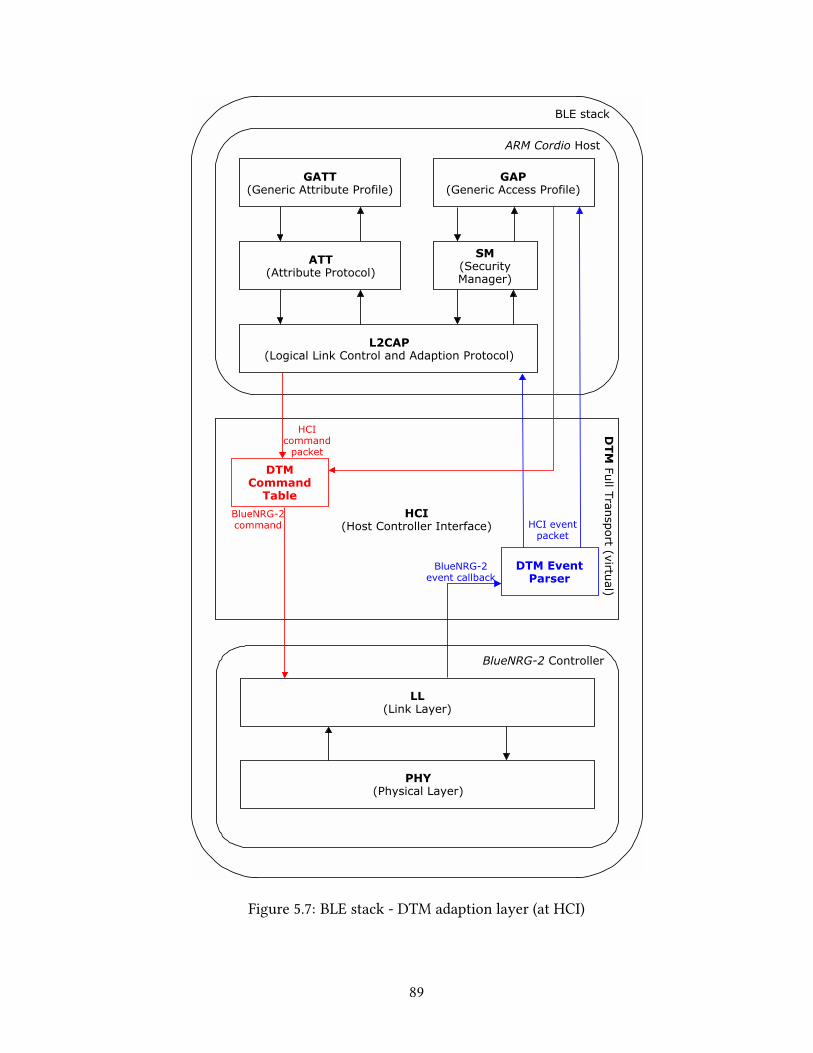
BLE stack
ARM Cordio Host
GATT (Generic Attribute Profile)
GAP (Generic Access Profile)
ATT (Attribute Protocol)
SM (SecurityManager)
L2CAP (Logical Link Control and Adaption Protocol)
HCI (Host Controller Interface)
BlueNRG2 Controller
LL (Link Layer)
PHY (Physical Layer)
DTM Full Transport (virtual)
DTMCommandTable
DTM EventParser
HCIcommandpacket
BlueNRG2command
BlueNRG2event callback
HCI eventpacket
Figure 5.7: BLE stack - DTM adaption layer (at HCI)
89

HCI command opcodes. Once resolved the opcode, the HCI command is executed by
pushing the HCI routine address in a function pointer, the rest of the host HCI packet
is parsed into PACKED5 structures organized according to the BlueNRG-2 required pa-
rameters for the command to be executed. �e command table is provided in Appendix
A, while the data structure implementing the function pointer mechanism is presented
in the next listing.
• on data received is a method whose purpose is to forward a packet coming from
the controller to the host, it is also “externalized” to be available to the C code of the
DTM parser (with name rcv callback).
/**** IN DTM HEADER ****/typedef uint16 t (*hci command process and response type)(uint8 t *
buffer in, uint16 t buffer in length, uint8 t *buffer out, uint16 tbuffer out max length) ;
typedef struct hci command table type s {uint16 t opcode;hci command process and response type execute;
} hci command table type;
An example of command parsing through the DTM adaption layer is provided in the fol-
lowing listing. Concerning BLE events, the parsing procedure is the opposite.typedef PACKED(struct) hci le set random address cp0 s {
uint8 t Random Address[6];} hci le set random address cp0;
uint16 t hci le set random address process(uint8 t *buffer in, uint16 tbuffer in length, uint8 t *buffer out, uint16 t buffer out max length)
{/* Input params */hci le set random address cp0 *cp0 = (hci le set random address cp0 *)(
buffer in + 1 + (0));
int output size = 1;/* Output params */uint8 t *status = (uint8 t *) (buffer out + 6);
if (buffer out max length < (1 + 6)) { return 0; }*status = hci le set random address(cp0−>Random Address /* 6 */);buffer out[0] = 0x04;buffer out[1] = 0x0E;buffer out[2] = output size + 3;buffer out[3] = 0x01;
5PACKED structures are data structures compiled without padding (to save memory).
90

buffer out[4] = 0x05;buffer out[5] = 0x20;return (output size + 6);
}
HCI Driver - HCIDriver
�is class inherits from the base class CordioHCIDriver. It shall provide:
• do initialize and do terminate, in this BlueNRG-2 driver they are not im-
plemented since controller initialization is performed at startup;
• get buffer pool description returns a 1430 bytes bu�er for the ARM Cordio
host to use;
• HCI reset sequence is started by start reset sequence, then the handler han-
dle reset sequence is performed until the reset procedure end is signaled by the
signal signal reset sequence done.
More in detail, the handle reset sequence provides initialization for BlueNRG-2
controller parameters, i.e. the LE event mask, that is a bit mask which events the controller
signals to the host and those to �ush. It provides also initialization for ARM Cordio runtime
parameters, such as Bluetooth address, controller bu�er size, supported state, whitelist size, LE
(Length Extension) features supported, resolving list size and maximum data length [21] [6].
TransportDriver and HCIDriver are provided in the �le BlueNrgHCIDriver.cpp,
while DTM adaption layer, due to huge amount of code, is not directly reported (as previously
said only the DTM command table is) in this document and provided at
https://github.com/ntoni92/mbed-os-BlueNRG2/blob/master/
targets/TARGET STMBLUE/DTM/src/DTM cmd db.c
5.4 Low power mode
As last step of the described porting activity there is the implementation of mechanisms that
allows BlueNRG-2 to save power in idle state through Mbed OS API. As explained in Chapter 1,
power saving is mandatory to make a BLE product a�ractive in an aggressive market context.
91

BlueNRG-2 natively provides three di�erent low power modes [27]:
• CPU-Halt mode
– �e least aggressive low power modes. CPU is stopped, but all device peripherals
are active and able to wake the CPU through interrupt.
• Sleep mode
– CPU and peripherals stopped, with the exception of the low speed oscillator and
external wake up sources (wake up virtual timers and GPIO pin 9, 10, 11, 12, 13).
– When wake up is triggered BlueNRG-2 reverts to its previous running mode a�er
the high speed oscillator stabilization.
• Standby mode
– CPU and all peripherals disabled, wake up sources are only GPIO pin 9, 10, 11, 12,
13.
– When wake up is triggered BlueNRG-2 reverts to its previous running mode a�er
the high speed oscillator stabilization.
On the Mbed OS side, the low power features are enabled by adding the “SLEEP” label
in the “device has” option of target’s section in the targets.json �le, described
in Section 5.1.1 [9]. A�er that, low power feature are enabled by providing a target-speci�c
implementation of the API mbed-os/hal/sleep api.h. �e la�er de�nes two low
power modes, hal sleep and hal deepsleep whose study is provided in Section 5.4.1
and 5.4.2 respectively and implementation is provided in Appendix A.
5.4.1 Sleep
In Mbed OS sleep mode the system core clock is disabled and RAM is put into data retention
state. In addition to that:
• any peripheral capable of generating interrupts must wake up the device;
92

• the device shall wake up within 10µs.
In addition to that, BlueNRG-2 controller requires to be queried and responds itself, ac-
cording to the state of the LL FSM, the sleep mode depth it can achieve.
Taking into account these design information, the only BlueNRG-2 sleep mode compatible
with Mbed OS is the CPU-Halt mode. For this reason the sleep manager is designed to query
the controller stack and if this check returns a deep sleep mode equal or greater than CPU-Halt
the CPU is halted (if this check fails the controller is not ready to sleep and thus the whole
system can’t sleep).
If the preliminary sleep check is passed there is no need to save peripheral registers (CPU-
Halt mode maintains con�gurations for all peripherals). �e only exception is the watchdog:
before sleep its control register value is saved (it will be restored right a�er wake up) and the
peripheral is disabled, to avoid a reset while CPU is halted.
5.4.2 Deep Sleep
In Mbed OS deep sleep mode the system core clock is disabled and RAM is put into data reten-
tion state. In addition to that:
• GPIO, RTC (Real Time Clock) or Low Power Ticker must wake up the CPU;
• the device shall wake up within 10ms.
�e same BlueNRG-2 stack controller query mechanism described for sleep mode in Section
5.4.1 is exploited to validate deep sleep request, but with respect to the la�er, for this mode a
return value higher than CPU-Halt is required.
However BlueNRG-2 hardware architecture presents a huge limitation in implementing
Mbed OS deep sleep mode: there is neither RTC nor hardware timer connected to the wake
up controller6. More precisely, there are two timers connected to the wake up controller, nev-
ertheless they are used from STMicroelectronics stack library, they are not directly accessible
as hardware peripherals but only through an interface provided in the header bluenrg1 stack.h
6An hardware timer connected to the wake up controller is required for implementing the Low Power Ticker,
that is in turn a wake up from deep sleep source.
93

(called Virtual Timers), and so quite useless for implementing an Mbed OS Low Power Ticker
(at least in a traditional way).
�e only available wake up peripheral is GPIO. �is represents an enormous limitation
in using deep sleep mode, since there is no way to schedule a wake up event at a certain
timestamp; this con�nes deep sleep to be used only in applications where wake up is required
to occur in a totally non-deterministic way and where there is there is an external access to
the system (resulting in a GPIO interrupt). One can see this deep sleep implementation only
as a porting exercise and something to evaluate bene�ts of BlueNRG-2 advanced sleep modes.
Concerning the implementation, when BlueNRG-2 goes in deep sleep, the peripheral reg-
isters values are lost. For this reason there are more operation to do before going into deep
sleep:
• save peripheral registers values into SRAM;
• save status into SRAM and disable watchdog;
• save application context (processor registers contents into SRAM);
• save MSP, PSP (Main and Process Stack Pointers) and PC (Program Counter) values into
SRAM.
�is setup completes the preliminary operations before going in deep sleep, and it has been
the last step in this experimental porting of ARM Mbed OS on BlueNRG-2 SoC.
5.5 Results and further developments
In this section there are presented some signi�cant results concerning the utilization of Mbed
OS operating system on BlueNRG-2. First of all there are reported information about com-
piled binary size and memory (Flash memory and SRAM occupation), a�er that there is a
functional veri�cation of an application (designed by ARM Mbed team and suggested as BLE
“Hello World”) and at the end there are some measurements concerning power consumption.
94

HRM - Heart Rate Monitor
�e presented HRM application has been taken as reference application while developing the
BlueNRG-2 Mbed OS porting, due to the fact that HRM pro�le requires the functionality of
almost all the BLE features (advertising, connection, service discovery, noti�cation) and so
it is a complete test for all the BLE stack layers. In addition to that, this approach has been
discussed and used in accordance with an internal ST team (located in France) working on the
Mbed OS porting on another BLE device, in order to exchange useful feedback about reciprocal
issues and progresses.
HRM has been useful also for another reason: it has been compiled and executed on an
already working and consolidated STMicroelectronics con�guration, a dual-chip over HCI
(NUCLEO-F401RE + X-NUCLEO-IDB05A1 BlueNRG-MS network coprocessor expansion, al-
ready mentioned in Chapter 1). Since the HCI is implemented through SPI, it has been possible
to extract the HCI trace resulting by correct execution of HRM, and use it as benchmark and
debug during BlueNRG-2 porting activity.
HRM code is reported in Appendix A.
5.5.1 Code size
�e following report tables refers to HRM code compiled with:
• GCC ARM toolchain 6.3.1 - 20170620 (release) [ARM/embedded-6-branch revision 249437]
• Mbed OS 5.11 [ARMmbed/mbed-os master branch, commit ID
df9ac85cbb38d8f06380b339398e73f968e3ba0a]
Considering that BlueNRG-2 controller is con�gured at its minimum (single link mode)
one can immediately notice that Mbed OS, also con�gured at its minimum (no RTOS), keeps
BlueNRG-2 memory to its limit: the free space for application is very tiny.
In debug mode moreover the printf (more in general the STDIO) cannot be called and has
to be disabled, otherwise the �nal code size exceeds Flash capacity.
In develop mode there is an improvement in terms of occupation, however in this con�gu-
ration debug symbols are removed from the executable (it means no live variables information
95

and no stepping mode execution) resulting in an increased di�culty in application develop.
Optimization level .text [B] .data [B] .bss [B]
-Os -g1 (optimize size) 213032 10600 7700
Table 5.1: Mbed OS HRM compiler report (develop con�guration)
Optimization level .text [B] .data [B] .bss [B]
-Og -g3 (optimize debug) 241600 10600 7828
Table 5.2: Mbed OS HRM compiler report (debug con�guration)
Flash (.text + .data) [B] SRAM (.data + .bss) [B]
HRM (develop pro�le) 223632 18300
HRM (debug pro�le) 251600 18428
Table 5.3: HRM code size and SRAM occupation
A possible trade o� could be to compile Mbed OS code with optimize-size options and the
user code with debug symbols enabled. A more aggressive solution could be (as ARM does
with Mbed OS 2 and OS 5 in its online compiler) to compile and provide Mbed OS 5 as static
binary library.
5.5.2 Power performances
�e last Mbed HRM testing on BlueNRG-2 concerns the power consumption of the system.
Considering the thesis work purpose, it is not interesting to characterize precisely the power
behavior of BlueNRG-2, but rather one could consider this part as an additional Mbed OS HRM
functional veri�cation on BlueNRG-2 (an more in general provide food for though regarding
what said on Bluetooth Low Energy technology in Chapter 1).
�e measurement setup is reported in Figure 5.8 and consists of:
• X-NUCLEO-LPM01A board for Nucleo expansion consumption measurement [33] (the
blue one);
96

• a X-NUCLEO expansion shield (the green top one) embedding a complete BlueNRG-2
System-on-Module, with RF frontend and ceramic antenna (the one in the metallic case
marked with “ES”).
Figure 5.8: STMicroelectronics “PowerShield” board and target BlueNRG-2 module expansion
power measurement setup
�e following is performed on this setup, instead of using the STEVAL-IDB008V2 board,
because it has only the BlueNRG-2 SoC (and not the accessory STEVAL ICs like, for instance,
the UART to USB interface).
Since the interest is in a qualitative power behavior, details about the measure itself are
omi�ed. Moreover the BlueNRG-2 System-On-Module is not commercial at the time when this
study has been carried on, additional information (like schematics and meaning of connectors)
97

cannot be provided since they are STMicroelectronics-restricted. Finally, one has to notice that
the proposed Mbed OS BLE API implementation on BlueNRG-2 does not support sleep modes
because of the lack of a wake up source (discussed at 5.3.1).
A dynamic current measure plot, with a sampling frequency of 10kHz, is provided in
Figure 5.9, generated by a so�ware GUI (STM32CubeMonitor-Power [34]) controlling the X-
NUCLEO-LPM01A through UART.
Figure 5.9: ARM Mbed OS HRM current trend during execution
Figure 5.9 shows BlueNRG-2 startup (POR) a�er about 2s, then it starts advertising with
1s interval (advertising events corresponds to 14mA peaks). At about 18s there is a connec-
tion from a central device and a service discovery request, the activity increases and average
current rises up, the central device enables noti�cations on the BlueNRG-2 HRM peripheral
and at about 23s it starts to notify the heart rate value (performed each second, but covered
from other device activity). At the end, a�er 35s, central device disconnects from HRM and it
starts advertising again.
During connection anything can be improved, however, as proposal of future search (since
at the time of this porting design is not feasible) it could be ideal to put the device in low
power mode during idle intervals occurring between advertising events (the la�er proposed
98

implementation puts BlueNRG-2 in sleep mode -5.4.1 - during these idle intervals). A simple
example in next section shows the potentially power saving with this strategy.
Low Power modes (further development)
Since BLE API is not compatible with deep sleep mode, this simple test has been designed
to show the current consumption trend of an application capable to go into the maximum
achievable power saving mode.
It is an application that blinks a LED every 2s. �is �rst plot (Figure 5.10) represents
the case in which BlueNRG-2 is fully active while the LED is on (the LED absorbed current
contributes in this phase) and is in sleep mode (CPU-Halt) when the LED is o�.
Figure 5.10: Sample LED Blink application with sleep mode
It presents a 2.5mA current consumption in idle phase, the same as the HRM example idle
phase between advertising events.
In the next example, shown in Figure 5.11, idle phase (LED o�) is spent in deep sleep mode
with a BlueNRG-2 Virtual Timer sets to wake up the device and turn on the LED every 2s.
�e code implementation of this last example is not reported, since it is coded in an hybrid
Mbed OS and bare direct calls to the STMicroelectronics BlueNRG-2 controller HAL, so not
99

compliant with Mbed OS guidelines.
Figure 5.11: Sample LED Blink application with deep sleep mode
One can notice that, out of idle phase, the consumption has not a regular trend. �is is due
to the fact that the wake up from deep sleep requires more operations with respect to sleep
case, involving oscillator re-calibration and a context restore. But above all, the most noticeable
information is the current consumption in idle deep sleep mode: it is less than 5µA.
5.5.3 Final considerations
Strictly concerning BlueNRG-2, collected data demonstrate not only that the coexistence of
ARM Mbed OS (with his BLE host stack ARM Cordio) and BlueNRG-2 HAL controller archi-
tecture is feasible, but that it makes sense to support this porting to reach the Mbed-enabled
status. �e only feature completely cut o� in this development is OTA - Over �e Air �rmware
update and programming: it is one of the most interesting features of BLE, but it requires a
huge amount of free memory to be implemented (this is not the case of this porting). Never-
theless, for those designs not requiring OTA, Mbed OS on BlueNRG-2 could be an interesting
solution. For this reason a merge pull-request has been opened with ARM, but there are some
features that ARM should introduce to support Cordio-based SoC design. �e most important
100

among the others is the capability of processing also the controller FSM at the same time (not
provided because, up to now, ARM Cordio host has been intended to work in a dual-chip con-
�guration when host and controller run on di�erent timing domains and communicate over
an asynchronous serial interface), so the possibility to register a callback that runs in the same
host tick context has been required to ARM. �is would allow to hide the stack synchronization
mechanism at the user level BLE API.
�e pull-request is available at the following URL:
https://github.com/ARMmbed/mbed-os/pull/9491.
More generally, this porting activity has been started with experimental and research pur-
poses. First and foremost this experience shows that, in embedded system design, good so�-
ware design strategies become every day more and more important and by now it is mandatory
to match a good electronic architecture to an e�cient �rmware construction. Let’s concen-
trate on power e�ciency discussed in the last activity of this chapter: consumption has a
strong cross-correlation with the code running on it, power has been reduced of many order
of magnitude only by changing �rmware design strategy. Translating these concepts into real
world, BLE technology is thought for ultra low power applications, mainly powered by coin-
cell ba�eries: it means that a �rmware has the “authority” to decide if ba�ery charge lasts
for six days or for six months. Whether the �rst option occurs while the second is expected
brings to destroy all the e�ort done for an excellent electronic/microelectronic design and
above all for the improvement of fabrication and miniaturization device technology, which in
the last few years is the primary R&D item of expenditure for a silicon foundry because of the
increasing cost-per-transistor trend.
Besides, experimenting this porting opens to the possibility in terms of �rmware reuse: in
the past a �rmware was more “bare metal” than today and thus strictly related to its hardware
and a change in the hardware architecture of the same product (for instance a new version of
the product) usually required a new �rmware. For this reason the concept of HAL - Hardware
Abstraction Layer has been introduced: a good co-design of the HAL-based �rmware avoids a
new bare-metal design of the la�er and allows to perform only a less invasive code refactoring
(for instance, on STM32 family microcontrollers, CubeMX HAL permits to easily migrate the
101

code between di�erent Cortex-M microcontrollers). Mbed OS is breaking again this paradigm
allowing to run the same code on di�erent architectures without changing any code line: for
instance it is possible the same identical HRM code either on a SoC (as BlueNRG-2 application
processor is) or on a dual-chip over HCI architecture (for instance NUCLEO + BlueNRG-MS
BLE co-processor).
For the discussed reasons STMicroelectronics, an excellence in semiconductor industry,
has began a reinforcing policy in its application design sector and to increase its asset also in
so�ware/�rmware solutions quality too. Moreover it has decided to reinforce its partnership
with ARM Mbed OS by starting to develop the support on other BLE devices. STMicroelec-
tronics considers Mbed OS support an important asset in its portfolio, and even if this project
has not the ambition to say if it absolutely correct or not, it adds a good reason to think that
is a reasonable choice.
102

Appendix A - Source Code
Microsecond Ticker - us ticker api.c
#include "us ticker api.h"#include "PeripheralNames.h"#include "hal types.h"#include "BlueNRG1 mft.h"#include "BlueNRG1 sysCtrl.h"#include "misc.h"
#define FREQ TICK 1000000#define NUMBITS 16
enum InitStatus{noinit = 0,init = 1,
}status;
const ticker info t *us ticker get info(){
static const ticker info t info = {FREQ TICK,NUMBITS
};return &info;
}
void us ticker isr(void){//clear interrupt flag and call the us ticker handlerMFT ClearIT(MFT2, MFT IT TND);us ticker irq handler();
}
void us ticker init(void){if(status == init) return;
status = init;
MFT InitType timer init;NVIC InitType NVIC InitStructure;
103

//tickcount = 0;
NVIC SetVector(MFT2B IRQn, (uint32 t)&us ticker isr);SysCtrl PeripheralClockCmd(CLOCK PERIPH MTFX2, ENABLE);MFT StructInit(&timer init);
timer init.MFT Mode = MFT MODE 3;timer init.MFT Prescaler = SYST CLOCK/FREQ TICK − 1;timer init.MFT Clock1 = MFT NO CLK;timer init.MFT Clock2 = MFT PRESCALED CLK;timer init.MFT CRA = 0x0000;timer init.MFT CRB = 0xFFFF;
MFT Init(MFT2, &timer init);
//Set counter for timer2MFT SetCounter2(MFT2, 0xFFFF);
//Enable MFT2B InterruptNVIC InitStructure.NVIC IRQChannel = MFT2B IRQn;NVIC InitStructure.NVIC IRQChannelPreemptionPriority =
HIGH PRIORITY;NVIC InitStructure.NVIC IRQChannelCmd = ENABLE;NVIC Init(&NVIC InitStructure);
//Enable the MFT2 interruptMFT EnableIT(MFT2, MFT IT TND, ENABLE);
//Start MTF2BMFT Cmd(MFT2, ENABLE);
}
void us ticker free(){if(status == init){
MFT Cmd(MFT2, DISABLE); //Disable MTF2BMFT DeInit(MFT2); //Deinit peripheralNVIC DisableIRQ(MFT2B IRQn); //Disable IRQSysCtrl PeripheralClockCmd(CLOCK PERIPH MTFX2, DISABLE);
//Disable Clock Gate peripheralstatus = noinit;
}}
uint32 t us ticker read(){if(!status)
us ticker init();//bitwise complement, MFT2 is a backward counter
return ˜MFT GetCounter2(MFT2);}
/* We get here absolute interrupt time which takes into account counteroverflow.
* Since we use additional count-DOWN timer to generate interrupt we needto calculate load value based on timestamp.
104

* If the timestamp value is higher than the actual count, then theinterrupt will be triggered after ”timestamp - actualticks”.* If the timestamp value is lower than the actual count, then theinterrupt is triggered at the next count cycle after the overflow,
i.e. ”timestamp + 1 x overflowcount (0xFFFF) - actualcount”.*/
void us ticker set interrupt(timestamp t timestamp){if(!status)
us ticker init();
uint16 t delta ticks = (uint16 t)(timestamp − us ticker read());//back counter
if (delta ticks == 0) {// The requested delay is less than the minimum resolution of this//counter.delta ticks = 1;
}//Clock Gate peripheral, safe since IRQ is disabled by high level APISysCtrl PeripheralClockCmd(CLOCK PERIPH MTFX2, DISABLE);
MFT2−>TNCRB = delta ticks;MFT EnableIT(MFT2, MFT IT TND, ENABLE);//Disable Clock Gate peripheralSysCtrl PeripheralClockCmd(CLOCK PERIPH MTFX2, ENABLE);
}
/* NOTE: following API implementations must be called with interruptsdisabled! */
void us ticker disable interrupt(void){if(!status)
us ticker init();MFT EnableIT(MFT2, MFT IT TND, DISABLE);
}
void us ticker clear interrupt(void){MFT ClearIT(MFT2, MFT IT TND);
}
void us ticker fire interrupt(void){NVIC SetPendingIRQ(MFT2B IRQn);
}
DTM Command Parsing - Command Table
/**** IN DTM IMPLEMENTATION ****/const hci command table type hci command table[57] = {
/* hcidisconnect */{0x0406, hci disconnect process},/* hcireadremoteversioninformation */{0x041d, hci read remote version information process},
105

/* hciseteventmask */{0x0c01, hci set event mask process},/* hcireset */{0x0c03, hci reset process},/* hcireadtransmitpowerlevel */{0x0c2d, hci read transmit power level process},/* hcireadlocalversioninformation */{0x1001, hci read local version information process},/* hcireadlocalsupportedcommands */{0x1002, hci read local supported commands process},/* hcireadlocalsupportedfeatures */{0x1003, hci read local supported features process},/* hcireadbdaddr */{0x1009, hci read bd addr process},/* hcireadrssi */{0x1405, hci read rssi process},/* hcileseteventmask */{0x2001, hci le set event mask process},/* hcilereadbuffersize */{0x2002, hci le read buffer size process},/* hcilereadlocalsupportedfeatures */{0x2003, hci le read local supported features process},/* hcilesetrandomaddress */{0x2005, hci le set random address process},/* hcilesetadvertisingparameters */{0x2006, hci le set advertising parameters process},/* hcilereadadvertisingchanneltxpower */{0x2007, hci le read advertising channel tx power process},/* hcilesetadvertisingdata */{0x2008, hci le set advertising data process},/* hcilesetscanresponsedata */{0x2009, hci le set scan response data process},/* hcilesetadvertiseenable */{0x200a, hci le set advertise enable process},/* hcilesetscanparameters */{0x200b, hci le set scan parameters process},/* hcilesetscanenable */{0x200c, hci le set scan enable process},/* hcilecreateconnection */{0x200d, hci le create connection process},/* hcilecreateconnectioncancel */{0x200e, hci le create connection cancel process},/* hcilereadwhitelistsize */{0x200f, hci le read white list size process},/* hcileclearwhitelist */{0x2010, hci le clear white list process},/* hcileadddevicetowhitelist */{0x2011, hci le add device to white list process},/* hcileremovedevicefromwhitelist */{0x2012, hci le remove device from white list process},/* hcileconnectionupdate */{0x2013, hci le connection update process},/* hcilesethostchannelclassification */{0x2014, hci le set host channel classification process},
106

/* hcilereadchannelmap */{0x2015, hci le read channel map process},/* hcilereadremoteusedfeatures */{0x2016, hci le read remote used features process},/* hcileencrypt */{0x2017, hci le encrypt process},/* hcilerand */{0x2018, hci le rand process},/* hcilestartencryption */{0x2019, hci le start encryption process},/* hcilelongtermkeyrequestreply */{0x201a, hci le long term key request reply process},/* hcilelongtermkeyrequestednegativereply */{0x201b, hci le long term key requested negative reply process},/* hcilereadsupportedstates */{0x201c, hci le read supported states process},/* hcilereceivertest */{0x201d, hci le receiver test process},/* hciletransmittertest */{0x201e, hci le transmitter test process},/* hciletestend */{0x201f, hci le test end process},/* hcilesetdatalength */{0x2022, hci le set data length process},/* hcilereadsuggesteddefaultdatalength */{0x2023, hci le read suggested default data length process},/* hcilewritesuggesteddefaultdatalength */{0x2024, hci le write suggested default data length process},/* hcilereadlocalp256publickey */{0x2025, hci le read local p256 public key process},/* hcilegeneratedhkey */{0x2026, hci le generate dhkey process},/* hcileadddevicetoresolvinglist */{0x2027, hci le add device to resolving list process},/* hcileremovedevicefromresolvinglist */{0x2028, hci le remove device from resolving list process},/* hcileclearresolvinglist */{0x2029, hci le clear resolving list process},/* hcilereadresolvinglistsize */{0x202a, hci le read resolving list size process},/* hcilereadpeerresolvableaddress */{0x202b, hci le read peer resolvable address process},/* hcilereadlocalresolvableaddress */{0x202c, hci le read local resolvable address process},/* hcilesetaddressresolutionenable */{0x202d, hci le set address resolution enable process},/* hcilesetresolvableprivateaddresstimeout */{0x202e, hci le set resolvable private address timeout process},/* hcilereadmaximumdatalength */{0x202f, hci le read maximum data length process},/* acihalwriteconfigdata */{0xfc0c, aci hal write config data process},/* acihalreadconfigdata */{0xfc0d, aci hal read config data process}
107

};
HCI Driver - BlueNrgHCIDriver.cpp
/********************************************************** @file BlueNrgHCIDriver.c* @author Antonio O.* @date 21 Dec. 2018********************************************************/
#include <mbed.h>#include "CordioHCIDriver.h"#include "CordioHCITransportDriver.h"#include "hci api.h"#include "hci cmd.h"#include "hci core.h"#include "dm api.h"#include "bstream.h"//#include "DTM boot.h"#include "DTM cmd db.h"#include "osal.h"#include "bluenrg1 api.h"#include "bluenrg1 stack.h"#include "hci defs.h"#include "BLEInstanceBase.h"
//STACKTICK CODE is used for emulating BTLE StackTick on an HCI vendor//specific command.//This value is not used and can be assigned to this functionality.//The wrapper for BTLE StackTick is providen in DTM command db header#define STACKTICK CODE 0xFCFF#define TICK US TICK MS*1000
extern ”C” void rcv callback(uint8 t *data, uint16 t len){ble::vendor::cordio::CordioHCITransportDriver::on data received(
data, len);}
#define HCI RESET RAND CNT 4#define LL WITHOUT HOST OFFSET 0x2C
namespace ble {namespace vendor {namespace bluenrg {
/*** BlueNRG HCI driver implementation.* @see cordio::CordioHCIDriver
108

*/
class HCIDriver : public cordio::CordioHCIDriver{public:
/*** Construction of the BlueNRG HCIDriver.* @param transport: Transport of the HCI commands.*/HCIDriver(cordio::CordioHCITransportDriver& transport driver) :
cordio::CordioHCIDriver(transport driver) { }
virtual ˜HCIDriver() {};/*** @see CordioHCIDriver::doinitialize*/
virtual void do initialize() {
}
/*** @see CordioHCIDriver::startresetsequence*/
virtual void start reset sequence() {/* send an HCI Reset command to start the sequence */HciResetCmd();
}
/*** @see CordioHCIDriver::doterminate*/
virtual void do terminate() {
}
/*** @see CordioHCIDriver::handleresetsequence*/
virtual void handle reset sequence(uint8 t *pMsg) {// only accept command complete event:if (*pMsg != HCI CMD CMPL EVT) {
return;}
uint8 t Value LL = 0x01;uint16 t opcode;
// static uint8t randCnt;
/* parse parameters */pMsg += HCI EVT HDR LEN;pMsg++; /* skip num packets */BSTREAM TO UINT16(opcode, pMsg); // copy opcodepMsg++; /* skip status */
109

/* decode opcode */switch (opcode){
case HCI OPCODE RESET:/* initialize rand command count */
// randCnt = 0;
//manually initialization of random address//(because there is no GAP init)
//8 bytes allocated because of ST random generationuint8 t Random Address[8];
hci le rand(Random Address);//bitwise or for 2 MSB (required by core 5.0 for Random Static Address)
Random Address[5] = Random Address[5] | 0xC0;
//Set the controller in Link Layer Only modeaci hal write config data(LL WITHOUT HOST OFFSET, 1, &
Value LL);hci le set random address(Random Address);
//DO NOT SET ANY EVENT MASK, BY DEFAULT ALL EVENTS ENABLED
// Ask the Bluetooth address of the controller.hci read bd addr(hciCoreCb.bdAddr);
// Read the size of the buffer of the controller and store the buffer//parameters in the stack Cordio runtime parameters.
hci le read buffer size(&hciCoreCb.bufSize, &hciCoreCb.numBufs);
/* initialize ACL buffer accounting */hciCoreCb.availBufs = hciCoreCb.numBufs;
// Read the states and state combinations supported by the link layer// of the controller and store supported state and combination in the//runtime parameters of the stack Cordio.
hci le read supported states(hciCoreCb.leStates);
// Read the total of whitelist entries that can be stored in the//controller and store the number of whitelist entries in the stack//Cordio runtime parameters.
hci le read white list size(&hciCoreCb.whiteListSize);
// Read the LE features supported by the controller and store the set// of LE features supported by the controller in the Cordio Stack//runtime parameters.
uint8 t features[2];//it is a 64 bit number, but only 16 MSB are significant (future use)
hci le read local supported features(features);hciCoreCb.leSupFeat = features[1] << 8 | features[0];
//reset sequence could terminate here depending on controller configuration
110

hciCoreReadResolvingListSize();
break;
case HCI OPCODE LE READ RES LIST SIZE:// Store the number of address translation entries in the stack// runtime parameter.
BSTREAM TO UINT8(hciCoreCb.resListSize, pMsg);
// Read the Controller maximum supported payload octets and packet// duration times for transmission and reception.
hciCoreReadMaxDataLen();break;
case HCI OPCODE LE READ MAX DATA LEN:{
// Store payload definition in the runtime stack parameters.uint16 t maxTxOctets;uint16 t maxTxTime;
BSTREAM TO UINT16(maxTxOctets, pMsg);BSTREAM TO UINT16(maxTxTime, pMsg);
/* use Controller’s maximum supported payload octets and packet* duration times for transmission as Host’s suggested values for* maximum transmission number of payload octets and maximum packet* transmission time for new connections.*/
HciLeWriteDefDataLen(maxTxOctets, maxTxTime);}break;
case HCI OPCODE LE WRITE DEF DATA LEN:if (hciCoreCb.extResetSeq){
/* send first extended command */(*hciCoreCb.extResetSeq)(pMsg, opcode);
}else{
/* initialize extended parameters */hciCoreCb.maxAdvDataLen = 0;hciCoreCb.numSupAdvSets = 0;hciCoreCb.perAdvListSize = 0;
/* send next command in sequence */HciLeRandCmd();
}break;
case HCI OPCODE LE READ MAX ADV DATA LEN:case HCI OPCODE LE READ NUM SUP ADV SETS:case HCI OPCODE LE READ PER ADV LIST SIZE:
// handle extended command
111

if (hciCoreCb.extResetSeq){
/* send next extended command in sequence */(*hciCoreCb.extResetSeq)(pMsg, opcode);
}break;
case HCI OPCODE LE RAND:/* last command in sequence set resetting state* and call callback */
signal reset sequence done();break;
default:break;
}}
virtual ble::vendor::cordio::buf pool desc tget buffer pool description() {uint8 t buffer[1430];static const wsfBufPoolDesc t pool desc[] = {
{ 16, 14 },{ 32, 10 },{ 64, 4 },{ 128, 2 },{ 272, 1 }
};
return ble::vendor::cordio::buf pool desc t(buffer, pool desc);}
private:
void hciCoreReadMaxDataLen(void){
/* if LE Data Packet Length Extensions is supported by Controller* and included */
if ((hciCoreCb.leSupFeat & HCI LE SUP FEAT DATA LEN EXT) &&(hciLeSupFeatCfg & HCI LE SUP FEAT DATA LEN EXT))
{/* send next command in sequence */
HciLeReadMaxDataLen();}else{
/* send next command in sequence */HciLeRandCmd();
}}
void hciCoreReadResolvingListSize(void){
/* if LL Privacy is supported by Controller and included */
112

if ((hciCoreCb.leSupFeat & HCI LE SUP FEAT PRIVACY) &&(hciLeSupFeatCfg & HCI LE SUP FEAT PRIVACY))
{/* send next command in sequence */
HciLeReadResolvingListSize();}else{
hciCoreCb.resListSize = 0;
/* send next command in sequence */hciCoreReadMaxDataLen();
}}
};
/*** Virtual Transport driver, used to exchange packet between host and* controller.*/
class TransportDriver : public cordio::CordioHCITransportDriver {public:
TransportDriver() : ble base(BLE::DEFAULT INSTANCE) {}
virtual ˜TransportDriver(){ }
/*** @see CordioHCITransportDriver::initialize*/
virtual void initialize() {/* Stack Initialization *///DTMStackInit();/* Periodic signal for BTLEStackTick initialization *///tick.attachus(callback(this, &StackTick), TICKMS*1000);tick.attach us(mbed::callback(this, &ble::vendor::bluenrg::
TransportDriver::StackTick), TICK US);}
/*** @see CordioHCITransportDriver::terminate*/
virtual void terminate() { }
/*** @see CordioHCITransportDriver::write*/
virtual uint16 t write(uint8 t type, uint16 t len, uint8 t *pData) {if(type== HCI CMD TYPE){
uint8 t resp len;resp len = process command(pData, len, buffer out, 255);rcv callback(buffer out, resp len);
}else if(type==HCI ACL TYPE){
113

uint16 t connHandle;uint16 t dataLen;uint8 t* pduData;uint8 t pb flag;uint8 t bc flag;
connHandle = ((pData[1] & 0x0F) << 8) + pData[0];dataLen = (pData[3] << 8) + pData[2];pduData = pData+4;pb flag = (pData[1] >> 4) & 0x3;bc flag = (pData[1] >> 6) & 0x3;hci tx acl data(connHandle, pb flag, bc flag, dataLen,
pduData);}
return len;}
private:uint16 t process command(uint8 t *buffer in, uint16 t buffer in length,
uint8 t *buffer out, uint16 t buffer out max length){uint16 t ret val, opCode;
Osal MemCpy(&opCode, buffer in, 2);for (uint i = 0; i < (sizeof(hci command table)/sizeof(
hci command table type)); i++) {if (opCode == hci command table[i].opcode) {
ret val = hci command table[i].execute(buffer in+2,buffer in length−2, buffer out, buffer out max length);
return ret val;}
}// Unknown command lengthbuffer out[0] = 0x04;buffer out[1] = 0x0F;buffer out[2] = 0x04;buffer out[3] = 0x01; ///01 unknown command ¡-buffer out[4] = 0x01;Osal MemCpy(&buffer out[5], &opCode, 2);return 7;
}
void StackTick(){ble base−>signalEventsToProcess(BLE::DEFAULT INSTANCE);
}
//buffer to store hci event packets generated after an hci commanduint8 t buffer out[258];Ticker tick;BLEInstanceBase* ble base;
};
} // namespace bluenrg} // namespace vendor
114

} // namespace ble
/*** Cordio HCI driver factory*/ble::vendor::cordio::CordioHCIDriver& ble cordio get hci driver() {
static ble::vendor::bluenrg::TransportDriver transport driver;static ble::vendor::bluenrg::HCIDriver hci driver(transport driver);return hci driver;
}
Low Power Mode - sleep api.c
/** sleepapi.h** Created on: 25 jan 2019* Author: Antonio O.*/
#if DEVICE SLEEP// IO13 — IO12 — IO11 — IO10 — IO9
#define GPIO WAKE BIT MASK 31// asserted pin in GPIOWAKEBITMASK are asserted at the value in the same//position of this mask#define GPIO WAKE LEVEL MASK 0
#define SHPR3 REG 0xE000ED20
#define WAKENED FROM IO9 0x09#define WAKENED FROM IO10 0x11#define WAKENED FROM IO11 0x21#define WAKENED FROM IO12 0x41#define WAKENED FROM IO13 0x81#define WAKENED FROM BLUE TIMER1 0x101#define WAKENED FROM BLUE TIMER2 0x401
#define LOW POWER STANDBY 0x03
#define BLUE CURRENT TIME REG 0x48000010
#include "sleep api.h"#include "bluenrg1 stack.h"#include "misc.h"#include "miscutil.h"
//BlueNRG2 sleepmodes typestypedef enum {
SLEEPMODE RUNNING = 0,
115

SLEEPMODE CPU HALT = 1,SLEEPMODE WAKETIMER = 2,SLEEPMODE NOTIMER = 3,
} SleepModes;
uint32 t cStackPreamble[CSTACK PREAMBLE NUMBER];volatile uint32 t* ptr ;
static void BlueNRG HaltCPU(void){// Store the watchdog configuration and the disable it to avoid reset//during CPU halt.
uint32 t WDG CR saved = WDG−>CR;WDG−>CR = 0;
// Wait for interrupt is called: the core execution is halted until an//event occurs.
WFI();
// Restore the watchdog functionality.WDG−>CR= WDG CR saved;
}
/** STMICROELECTRONICS DEEP SLEEP IMPLEMENTATION **/static void BlueNRG DeepSleep(SleepModes sleepMode, uint8 t gpioWakeBitMask
){uint32 t savedCurrentTime, nvicPendingMask;PartInfoType partInfo;uint8 t i;/* System Control saved */uint32 t SYS Ctrl saved;/* NVIC Information Saved */uint32 t NVIC ISER saved, NVIC IPR saved[8], PENDSV SYSTICK IPR saved;/* CKGEN SOC Enabled */uint32 t CLOCK EN saved;/* GPIO Information saved */uint32 t GPIO DATA saved, GPIO OEN saved, GPIO PE saved, GPIO DS saved,
GPIO IS saved, GPIO IBE saved;uint32 t GPIO IEV saved, GPIO IE saved, GPIO MODE0 saved,
GPIO MODE1 saved, GPIO IOSEL MFTX saved;#ifdef BLUENRG2 DEVICE
uint32 t GPIO MODE2 saved, GPIO MODE3 saved;#endif
/* UART Information saved */uint32 t UART TIMEOUT saved, UART LCRH RX saved, UART IBRD saved,
UART FBRD saved;uint32 t UART LCRH TX saved, UART CR saved, UART IFLS saved,
UART IMSC saved;uint32 t UART DMACR saved, UART XFCR saved, UART XON1 saved,
UART XON2 saved;uint32 t UART XOFF1 saved, UART XOFF2 saved;/* SPI Information saved */uint32 t SPI CR0 saved, SPI CR1 saved, SPI CPSR saved, SPI IMSC saved,
SPI DMACR saved;
116

uint32 t SPI RXFRM saved, SPI CHN saved, SPI WDTXF saved;/* I2C Information saved */uint32 t I2C CR saved[2], I2C SCR saved[2], I2C TFTR saved[2],
I2C RFTR saved[2];uint32 t I2C DMAR saved[2], I2C BRCR saved[2], I2C IMSCR saved[2],
I2C THDDAT saved[2];uint32 t I2C THDSTA FST STD saved[2], I2C TSUSTA FST STD saved[2];/* RNG Information saved */uint32 t RNG CR saved;/* SysTick Information saved */uint32 t SYST CSR saved, SYST RVR saved;/* RTC Information saved */uint32 t RTC CWDMR saved, RTC CWDLR saved, RTC CWYMR saved,
RTC CWYLR saved, RTC CTCR saved;uint32 t RTC IMSC saved, RTC TCR saved, RTC TLR1 saved, RTC TLR2 saved,
RTC TPR1 saved;uint32 t RTC TPR2 saved, RTC TPR3 saved, RTC TPR4 saved;/* MFTX Information saved */uint32 t T1CRA saved, T1CRB saved, T1PRSC saved, T1CKC saved,
T1MCTRL saved, T1ICTRL saved;uint32 t T2CRA saved, T2CRB saved, T2PRSC saved, T2CKC saved,
T2MCTRL saved, T2ICTRL saved;/* WDT Information saved */uint32 t WDG LR saved, WDG CR saved, WDG LOCK saved;/* DMA channel [0..7] Information saved */uint32 t DMA CCR saved[8], DMA CNDTR saved[8], DMA CPAR saved[8],
DMA CMAR[8];/* ADC Information saved */uint32 t ADC CTRL saved, ADC CONF saved, ADC IRQMASK saved,
ADC OFFSET LSB saved, ADC OFFSET MSB saved;uint32 t ADC THRESHOLD HI saved, ADC THRESHOLD LO saved;/* FlASH Config saved */uint32 t FLASH CONFIG saved;/* PKA Information saved */uint32 t PKA IEN saved;
/* Get partInfo */HAL GetPartInfo(&partInfo);
/* Save the peripherals configuration *//* System Control */SYS Ctrl saved = SYSTEM CTRL−>CTRL;/* FLASH CONFIG */FLASH CONFIG saved = FLASH−>CONFIG;/* NVIC */NVIC ISER saved = NVIC−>ISER[0];
// Issue with Atollic compiler// memcpy(NVICIPRsaved, (void const *)NVIC-¿IP, sizeof(NVICIPRsaved));
for (i=0; i<8; i++) {NVIC IPR saved[i] = NVIC−>IP[i];
}
117

PENDSV SYSTICK IPR saved = *(volatile uint32 t *)SHPR3 REG;/* CKGEN SOC Enabled */CLOCK EN saved = CKGEN SOC−>CLOCK EN;/* GPIO */GPIO DATA saved = GPIO−>DATA;GPIO OEN saved = GPIO−>OEN;GPIO PE saved = GPIO−>PE;GPIO DS saved = GPIO−>DS;GPIO IS saved = GPIO−>IS;GPIO IBE saved = GPIO−>IBE;GPIO IEV saved = GPIO−>IEV;GPIO IE saved = GPIO−>IE;GPIO MODE0 saved = GPIO−>MODE0;GPIO MODE1 saved = GPIO−>MODE1;
#ifdef BLUENRG2 DEVICEGPIO MODE2 saved = GPIO−>MODE2;GPIO MODE3 saved = GPIO−>MODE3;
#endifGPIO IOSEL MFTX saved = GPIO−>MFTX;/* UART */UART TIMEOUT saved = UART−>TIMEOUT;UART LCRH RX saved = UART−>LCRH RX;UART IBRD saved = UART−>IBRD;UART FBRD saved = UART−>FBRD;UART LCRH TX saved = UART−>LCRH TX;UART CR saved = UART−>CR;UART IFLS saved = UART−>IFLS;UART IMSC saved = UART−>IMSC;UART DMACR saved = UART−>DMACR;UART XFCR saved = UART−>XFCR;UART XON1 saved = UART−>XON1;UART XON2 saved = UART−>XON2;UART XOFF1 saved = UART−>XOFF1;UART XOFF2 saved = UART−>XOFF2;/* SPI */SPI CR0 saved = SPI1−>CR0;SPI CR1 saved = SPI1−>CR1;SPI CPSR saved = SPI1−>CPSR;SPI IMSC saved = SPI1−>IMSC;SPI DMACR saved = SPI1−>DMACR;SPI RXFRM saved = SPI1−>RXFRM;SPI CHN saved = SPI1−>CHN;SPI WDTXF saved = SPI1−>WDTXF;/* I2C */for (i=0; i<2; i++) {
I2C Type *I2Cx = (I2C Type*)(I2C2 BASE+ 0x100000*i);I2C CR saved[i] = I2Cx−>CR;I2C SCR saved[i] = I2Cx−>SCR;I2C TFTR saved[i] = I2Cx−>TFTR;I2C RFTR saved[i] = I2Cx−>RFTR;I2C DMAR saved[i] = I2Cx−>DMAR;I2C BRCR saved[i] = I2Cx−>BRCR;I2C IMSCR saved[i] = I2Cx−>IMSCR;I2C THDDAT saved[i] = I2Cx−>THDDAT;
118

I2C THDSTA FST STD saved[i] = I2Cx−>THDSTA FST STD;I2C TSUSTA FST STD saved[i] = I2Cx−>TSUSTA FST STD;
}/* RNG */RNG CR saved = RNG−>CR;/* RTC */RTC CWDMR saved = RTC−>CWDMR;RTC CWDLR saved = RTC−>CWDLR;RTC CWYMR saved = RTC−>CWYMR;RTC CWYLR saved = RTC−>CWYLR;RTC CTCR saved = RTC−>CTCR;RTC IMSC saved = RTC−>IMSC;RTC TCR saved = RTC−>TCR;RTC TLR1 saved = RTC−>TLR1;RTC TLR2 saved = RTC−>TLR2;RTC TPR1 saved = RTC−>TPR1;RTC TPR2 saved = RTC−>TPR2;RTC TPR3 saved = RTC−>TPR3;RTC TPR4 saved = RTC−>TPR4;/* MFTX */T1CRA saved = MFT1−>TNCRA;T1CRB saved = MFT1−>TNCRB;T1PRSC saved = MFT1−>TNPRSC;T1CKC saved = MFT1−>TNCKC;T1MCTRL saved = MFT1−>TNMCTRL;T1ICTRL saved = MFT1−>TNICTRL;T2CRA saved = MFT2−>TNCRA;T2CRB saved = MFT2−>TNCRB;T2PRSC saved = MFT2−>TNPRSC;T2CKC saved = MFT2−>TNCKC;T2MCTRL saved = MFT2−>TNMCTRL;T2ICTRL saved = MFT2−>TNICTRL;/* SysTick */SYST CSR saved = SysTick−>CTRL;SYST RVR saved = SysTick−>LOAD;/* WDT */WDG LR saved = WDG−>LR;WDG CR saved = WDG−>CR;if(WDG−>LOCK == 0) {
WDG LOCK saved = 0x1ACCE551;} else {WDG LOCK saved = 0;
}/* DMA */for (i=0; i<8; i++) {
DMA CH Type *DMAx = (DMA CH Type*)(DMA CH0 BASE+ 0x14*i);DMA CNDTR saved[i] = DMAx−>CNDTR;DMA CCR saved[i] = DMAx−>CCR;DMA CPAR saved[i] = DMAx−>CPAR;DMA CMAR[i] = DMAx−>CMAR;
}/* ADC */ADC CONF saved = ADC−>CONF;ADC IRQMASK saved = ADC−>IRQMASK;
119

ADC OFFSET MSB saved = ADC−>OFFSET MSB;ADC OFFSET LSB saved = ADC−>OFFSET LSB;ADC THRESHOLD HI saved = ADC−>THRESHOLD HI;ADC THRESHOLD LO saved = ADC−>THRESHOLD LO;ADC CTRL saved = ADC−>CTRL;
/* PKA */PKA IEN saved = PKA−>IEN;
// Enable the STANDBY modeif (sleepMode == SLEEPMODE NOTIMER) {
BLUE CTRL−>TIMEOUT |= LOW POWER STANDBY<<28;}
//Save the CSTACK number of words that will be restored at wakeup reseti = 0;ptr = vector table[0]. ptr ;ptr −= CSTACK PREAMBLE NUMBER;do {
cStackPreamble[i] = *ptr;i++;ptr++;
} while (i < CSTACK PREAMBLE NUMBER);
if (((partInfo.die major<<4)|(partInfo.die cut)) >= WA DEVICE VERSION) {/* Lock the flash */flash sw lock = FLASH LOCK WORD;/* Disable BOR */SET BORconfigStatus(FALSE);
}
//Enable deep sleepSystemSleepCmd(ENABLE);//The disable irq() used at the beginning of the BlueNRGSleep()//function//masks all the interrupts. The interrupts will be enabled at the end of//the context restore. Now induce a context save.void CS contextSave(void);CS contextSave();
//Disable deep sleep, because if no reset occurs for an interrupt//pending, the register value remain set and if a simple CPUHALT command//is called from the application the BlueNRG-1 enters in deep sleep//without make a context save.//So, exiting from the deep sleep the context is restored with//wrong random value.SystemSleepCmd(DISABLE);
if (!wakeupFromSleepFlag) {if((NVIC−>ISPR[0]&(1<<BLUE CTRL IRQn)) == 0) {
//At this stage the Blue Control Interrupt shall not be pending.//So, if this happens means that the application has called the//BlueNRGSleep() API with the wakeup source already acrive.//In this scenario we don’t need to wait the 91 us, otherwise
120

//the radio activity will be compromised.nvicPendingMask = savedNVIC ISPR ˆ NVIC−>ISPR[0];if ((savedSHCSR != SCB−>SHCSR) | |
//Verified if a SVCall Interrupt is pending((savedNVIC ISPR != NVIC−>ISPR[0]) && (nvicPendingMask & NVIC−>
ISER[0]))//Verified if a NVIC Interrupt is pending
((savedICSR & 0x10000000) != (SCB−>ICSR & 0x10000000)) | |// Verified if a PendSV interrupt is pending
(((savedICSR & 0x4000000) != (SCB−>ICSR & 0x4000000)) && (SysTick−>CTRL & 0x02))) {
// Verified if a SysTick interrupt is pendingsavedCurrentTime = (*(volatile uint32 t *)BLUE CURRENT TIME REG) >>
4;if (0xFFFFF >= (savedCurrentTime+3)) {
//Check if the counter are wrappingwhile ((savedCurrentTime+3) > ((*(volatile uint32 t *)
BLUE CURRENT TIME REG) >> 4)); //Not Wrap} else {
while (((*(volatile uint32 t *)BLUE CURRENT TIME REG) >> 4) != (savedCurrentTime + 3 − 0xFFFFF)); //Wrap
}}
}
if (((partInfo.die major<<4)|(partInfo.die cut)) >= WA DEVICE VERSION){
/* Restore BOR configuration */SET BORconfigStatus(TRUE);/* Unlock the flash */flash sw lock = FLASH UNLOCK WORD;
}
// Disable the STANDBY modeif (sleepMode == SLEEPMODE NOTIMER) {
BLUE CTRL−>TIMEOUT &= ˜(LOW POWER STANDBY<<28);}
} else {
/* Start a new calibration, needed to signal if the HS is ready */CKGEN BLE−>CLK32K IT = 1;CKGEN BLE−>CLK32K COUNT = 0;CKGEN BLE−>CLK32K PERIOD = 0;
// Restore the CSTACK number of words that will be saved before the sleepi = 0;ptr = vector table[0]. ptr ;ptr −= CSTACK PREAMBLE NUMBER;do {
*ptr = cStackPreamble[i];i++;ptr++;
} while (i < CSTACK PREAMBLE NUMBER);
121

/* Restore the peripherals configuration *//* FLASH CONFIG */FLASH−>CONFIG = FLASH CONFIG saved;/* NVIC */NVIC−>ISER[0] = NVIC ISER saved;
for (i=0; i<8; i++) {NVIC−>IP[i] = NVIC IPR saved[i];
}
*(volatile uint32 t *)SHPR3 REG = PENDSV SYSTICK IPR saved;/* CKGEN SOC Enabled */CKGEN SOC−>CLOCK EN = CLOCK EN saved;/* GPIO */GPIO−>DATA = GPIO DATA saved;GPIO−>OEN = GPIO OEN saved;GPIO−>PE = GPIO PE saved;GPIO−>DS = GPIO DS saved;GPIO−>IEV = GPIO IEV saved;GPIO−>IBE = GPIO IBE saved;GPIO−>IS = GPIO IS saved;GPIO−>IC = GPIO IE saved;GPIO−>IE = GPIO IE saved;GPIO−>MODE0 = GPIO MODE0 saved;GPIO−>MODE1 = GPIO MODE1 saved;
#ifdef BLUENRG2 DEVICEGPIO−>MODE2 = GPIO MODE2 saved;GPIO−>MODE3 = GPIO MODE3 saved;
#endifGPIO−>MFTX = GPIO IOSEL MFTX saved;/* UART */UART−>TIMEOUT = UART TIMEOUT saved;UART−>LCRH RX = UART LCRH RX saved;UART−>IBRD = UART IBRD saved;UART−>FBRD = UART FBRD saved;UART−>LCRH TX = UART LCRH TX saved;UART−>CR = UART CR saved;UART−>IFLS = UART IFLS saved;UART−>IMSC = UART IMSC saved;UART−>DMACR = UART DMACR saved;UART−>XFCR = UART XFCR saved;UART−>XON1 = UART XON1 saved;UART−>XON2 = UART XON2 saved;UART−>XOFF1 = UART XOFF1 saved;UART−>XOFF2 = UART XOFF2 saved;/* SPI */SPI1−>CR0 = SPI CR0 saved;SPI1−>CR1 = SPI CR1 saved;SPI1−>CPSR = SPI CPSR saved;SPI1−>IMSC = SPI IMSC saved;SPI1−>DMACR = SPI DMACR saved;SPI1−>RXFRM = SPI RXFRM saved;
122

SPI1−>CHN = SPI CHN saved;SPI1−>WDTXF = SPI WDTXF saved;/* I2C */for (i=0; i<2; i++) {
I2C Type *I2Cx = (I2C Type*)(I2C2 BASE+ 0x100000*i);I2Cx−>CR = I2C CR saved[i];I2Cx−>SCR = I2C SCR saved[i];I2Cx−>TFTR = I2C TFTR saved[i];I2Cx−>RFTR = I2C RFTR saved[i];I2Cx−>DMAR = I2C DMAR saved[i];I2Cx−>BRCR = I2C BRCR saved[i];I2Cx−>IMSCR = I2C IMSCR saved[i];I2Cx−>THDDAT = I2C THDDAT saved[i];I2Cx−>THDSTA FST STD = I2C THDSTA FST STD saved[i];I2Cx−>TSUSTA FST STD = I2C TSUSTA FST STD saved[i];
}/* RNG */RNG−>CR = RNG CR saved;/* SysTick */SysTick−>LOAD = SYST RVR saved;SysTick−>VAL = 0;SysTick−>CTRL = SYST CSR saved;/* RTC */RTC−>CWDMR = RTC CWDMR saved;RTC−>CWDLR = RTC CWDLR saved;RTC−>CWYMR = RTC CWYMR saved;RTC−>CWYLR = RTC CWYLR saved;RTC−>CTCR = RTC CTCR saved;RTC−>IMSC = RTC IMSC saved;RTC−>TLR1 = RTC TLR1 saved;RTC−>TLR2 = RTC TLR2 saved;RTC−>TPR1 = RTC TPR1 saved;RTC−>TPR2 = RTC TPR2 saved;RTC−>TPR3 = RTC TPR3 saved;RTC−>TPR4 = RTC TPR4 saved;/* Enable moved at the end of RTC configuration */RTC−>TCR = RTC TCR saved;/* MFTX */MFT1−>TNCRA = T1CRA saved;MFT1−>TNCRB = T1CRB saved;MFT1−>TNPRSC = T1PRSC saved;MFT1−>TNCKC = T1CKC saved;MFT1−>TNMCTRL = T1MCTRL saved;MFT1−>TNICTRL = T1ICTRL saved;MFT2−>TNCRA = T2CRA saved;MFT2−>TNCRB = T2CRB saved;MFT2−>TNPRSC = T2PRSC saved;MFT2−>TNCKC = T2CKC saved;MFT2−>TNMCTRL = T2MCTRL saved;MFT2−>TNICTRL = T2ICTRL saved;/* WDT */WDG−>LR = WDG LR saved;WDG−>CR = WDG CR saved;WDG−>LOCK = WDG LOCK saved;
123

/* DMA */for (i=0; i<8; i++) {
DMA CH Type *DMAx = (DMA CH Type*)(DMA CH0 BASE+ 0x14*i);DMAx−>CNDTR = DMA CNDTR saved[i];DMAx−>CCR = DMA CCR saved[i] ;DMAx−>CPAR = DMA CPAR saved[i];DMAx−>CMAR = DMA CMAR[i];
}/* ADC */ADC−>CONF = ADC CONF saved;ADC−>IRQMASK = ADC IRQMASK saved;ADC−>OFFSET MSB = ADC OFFSET MSB saved;ADC−>OFFSET LSB = ADC OFFSET LSB saved;ADC−>THRESHOLD HI = ADC THRESHOLD HI saved;ADC−>THRESHOLD LO = ADC THRESHOLD LO saved;ADC−>CTRL = ADC CTRL saved;
/* PKA */PKA−>IEN = PKA IEN saved;//The five IRQs are linked to a real ISR. If any of the five IRQs//triggered, then pend their ISR//Capture the wake source from the BLEREASONRESET registerif ((CKGEN SOC−>REASON RST == 0) &&
(CKGEN BLE−>REASON RST >= WAKENED FROM IO9) &&(CKGEN BLE−>REASON RST <= WAKENED FROM IO13) &&
gpioWakeBitMask) {if ((((CKGEN BLE−>REASON RST & WAKENED FROM IO9) ==
WAKENED FROM IO9) && (GPIO−>IE & GPIO Pin 9)) | |(((CKGEN BLE−>REASON RST & WAKENED FROM IO10) ==
WAKENED FROM IO10) && (GPIO−>IE & GPIO Pin 10)) | |(((CKGEN BLE−>REASON RST & WAKENED FROM IO11) ==
WAKENED FROM IO11) && (GPIO−>IE & GPIO Pin 11)) | |(((CKGEN BLE−>REASON RST & WAKENED FROM IO12) ==
WAKENED FROM IO12) && (GPIO−>IE & GPIO Pin 12)) | |(((CKGEN BLE−>REASON RST & WAKENED FROM IO13) ==
WAKENED FROM IO13) && (GPIO−>IE & GPIO Pin 13))){
NVIC−>ISPR[0] = 1<<GPIO IRQn;}
}
// Disable the STANDBY modeif (sleepMode == SLEEPMODE NOTIMER) {
BLUE CTRL−>TIMEOUT &= ˜(LOW POWER STANDBY<<28);}
//Restore the System Control register to indicate which HS crystal is usedSYSTEM CTRL−>CTRL = SYS Ctrl saved;
// Wait until the HS clock is ready.// If SLEEPMODENOTIMER is set, wait the LS clock is ready.if (sleepMode == SLEEPMODE NOTIMER) {
DeviceConfiguration(FALSE, TRUE);} else {
124

DeviceConfiguration(FALSE, FALSE);}
/* If the HS is a 32 MHz */if (SYS Ctrl saved & 1) {
#if (FORCE CORE TO 16MHZ == 1)/* AHB up converter command register write*/AHBUPCONV−>COMMAND = 0x14;
#else/* AHB up converter command register write*/AHBUPCONV−>COMMAND = 0x15;
#endif}
}
//We can clear PRIMASK to reenable global interrupt operation.// enable irq(); //done in haldeepsleep
}
void hal sleep(void){//only CPU halt, wakeup from any interrupt source//wakeup timer is not available
// Disable IRQscore util critical section enter();
//Flag to signal if a wakeup from standby or sleep occurredwakeupFromSleepFlag = 0;
//ask the BLE controller if link layer termination is ongoing,//to go sleep at least it shall return at least SLEEPMODECPUHALTSleepModes sleepMode allowed = (SleepModes)
BlueNRG Stack Perform Deep Sleep Check();
if(sleepMode allowed >= SLEEPMODE CPU HALT){BlueNRG HaltCPU();
}// Unmask all the interruptcore util critical section exit();
}
void hal deepsleep(void){//check no active UART RX - when tx ongoing fifo empty flag is 0 (RESET)#if DEVICE SERIAL
serialTxActive();#endif
// Disable IRQscore util critical section enter();
//Flag to signal if a wakeup from standby or sleep occurredwakeupFromSleepFlag = 0;
125

//ask the BLE controller if link layer termination is ongoing,//to go sleep at least it shall return at least SLEEPMODEWAKETIMER - only//GPIO wakeup available
volatile SleepModes sleepMode allowed = (SleepModes)BlueNRG Stack Perform Deep Sleep Check();
switch(sleepMode allowed){case SLEEPMODE CPU HALT:
BlueNRG HaltCPU();break;
case SLEEPMODE WAKETIMER:case SLEEPMODE NOTIMER:
//Setup the GPIO Wakeup Source//sleepModeallowed = SLEEPMODEWAKETIMER;SYSTEM CTRL−>WKP IO IS = GPIO WAKE LEVEL MASK;SYSTEM CTRL−>WKP IO IE = GPIO WAKE BIT MASK;BlueNRG DeepSleep(sleepMode allowed,GPIO WAKE BIT MASK);break;
default:break;
}// Unmask all the interruptcore util critical section exit();
}
#endif //DEVICE SLEEP
ARMMbed OS HRM (Heart Rate Monitor) - main.cpp
/* mbed Microcontroller Library* Copyright (c) 2006-2015 ARM Limited** Licensed under the Apache License, Version 2.0 (the ”License”);* you may not use this file except in compliance with the License.* You may obtain a copy of the License at** http://www.apache.org/licenses/LICENSE-2.0** Unless required by applicable law or agreed to in writing, software* distributed under the License is distributed on an ”AS IS” BASIS,* WITHOUT WARRANTIES OR CONDITIONS OF ANY KIND, either express or implied.* See the License for the specific language governing permissions and* limitations under the License.*/
#include <events/mbed events.h>#include <mbed.h>#include "ble/BLE.h"#include "ble/gap/Gap.h"#include "ble/services/HeartRateService.h"
126

#include "pretty printer.h"
const static char DEVICE NAME[] = ”ORLHRM”;
static events::EventQueue event queue(/* event count */ 16 *EVENTS EVENT SIZE);
class HeartrateDemo : ble::Gap::EventHandler {public:
HeartrateDemo(BLE &ble, events::EventQueue &event queue) :ble(ble),event queue(event queue),led1(LED1, 1),connected(false),hr uuid(GattService::UUID HEART RATE SERVICE),hr counter(100),hr service(ble, hr counter, HeartRateService::LOCATION FINGER),adv data builder( adv buffer) { }
void start() {ble.gap().setEventHandler(this);
ble.init(this, &HeartrateDemo::on init complete);
event queue.call every(500, this, &HeartrateDemo::blink);event queue.call every(1000, this, &HeartrateDemo::
update sensor value);
event queue.dispatch forever();}
private://Callback triggered when the ble initialization process has finishedvoid on init complete(BLE::InitializationCompleteCallbackContext *
params) {if (params−>error != BLE ERROR NONE) {
printf(”Ble initialization failed.”);return;
}
print mac address();
start advertising();}
void start advertising() {/* Create advertising parameters and payload */
ble::AdvertisingParameters adv parameters(ble::advertising type t::CONNECTABLE UNDIRECTED,ble::adv interval t(ble::millisecond t(1000))
);
adv data builder.setFlags();
127

adv data builder.setAppearance(ble::adv data appearance t::GENERIC HEART RATE SENSOR);
adv data builder.setLocalServiceList(mbed::make Span(& hr uuid, 1));
adv data builder.setName(DEVICE NAME);
/* Setup advertising */
ble error t error = ble.gap().setAdvertisingParameters(ble::LEGACY ADVERTISING HANDLE,adv parameters
);
if (error) {printf(”ble.gap().setAdvertisingParameters() failed“r“n”);return;
}
error = ble.gap().setAdvertisingPayload(ble::LEGACY ADVERTISING HANDLE,adv data builder.getAdvertisingData()
);
if (error) {printf(”ble.gap().setAdvertisingPayload() failed“r“n”);return;
}
/* Start advertising */
error = ble.gap().startAdvertising(ble::LEGACY ADVERTISING HANDLE);
if (error) {printf(”ble.gap().startAdvertising() failed“r“n”);return;
}}
void update sensor value() {if ( connected) {
// Do blocking calls or whatever is necessary for sensor polling.// In our case, we simply update the HRM measurement.
hr counter++;
// 100 ¡= HRM bps ¡=175if ( hr counter == 175) {
hr counter = 100;}
hr service.updateHeartRate( hr counter);}
}
128

void blink(void) {led1 = ! led1;
}
private:/* Event handler */
void onDisconnectionComplete(const ble::DisconnectionCompleteEvent&) {ble.gap().startAdvertising(ble::LEGACY ADVERTISING HANDLE);connected = false;
}
virtual void onConnectionComplete(const ble::ConnectionCompleteEvent &event) {if (event.getStatus() == BLE ERROR NONE) {
connected = true;}
}
private:BLE & ble;events::EventQueue & event queue;DigitalOut led1;
bool connected;
UUID hr uuid;
uint8 t hr counter;HeartRateService hr service;
uint8 t adv buffer[ble::LEGACY ADVERTISING MAX SIZE];ble::AdvertisingDataBuilder adv data builder;
};
//Schedule processing of events from the BLE middleware in the event queue.void schedule ble events(BLE::OnEventsToProcessCallbackContext *context) {
event queue.call(Callback<void()>(&context−>ble, &BLE::processEvents));}
int main(){
BLE &ble = BLE::Instance();ble.onEventsToProcess(schedule ble events);
HeartrateDemo demo(ble, event queue);demo.start();
return 0;}
129

130

Appendix B - Toolchain Setup
In this Appendix there is explained how to con�gure an Eclipse CDT-based free development
environment for mbed-OS, as an alternative to the priced counterparts (IAR EWARM, Keil
µVision) and the ST supported toolchain Atollic TrueSTUDIO (that is currently under devel-
opment).
�e given con�guration has been used during the BlueNRG-2 Mbed OS porting activity.
Prerequisites
To ensure a correct management of binary installation (and future updates of them), it is useful
to use xpm, a package manager built on a javascript runtime (Node.js), that allows an high
portability on di�erent development platform and a correct organization of the folder hier-
archy (in such a way Eclipse is able to resolve all its path dependencies) [13]. �e following
description relies on the use of xpm.
First of all, the following elements must be installed:
1. ARM toolchain, by using the command:
$ xpm install --global @gnu-mcu-eclipse/arm-none-eabi-gcc
2. �is step is Windows speci�c, it provides, among the others, make.exe:
$ xpm install --global @gnu-mcu-eclipse/windows-build-tools
3. OpenOCD, a so�ware interface for the STM ST-Link debugger:
$ xpm install --global @gnu-mcu-eclipse/openocd
4. Java Development Kit (through its installation wizard) [18].
131

5. Eclipse-CDT with MCU plugins. �e simplest way to get it is to download a ready-to-go
version from the GNU MCU Eclipse webpage. [13].
6. mbed-CLI (through its installation wizard) [10].
C/C++ Build
Using the classic Eclipse C/C++ toolchain (GCC ARM, based on the autogeneration of make�le
provided by Mbed-OS python exporters and Eclipse CDT) is feasible, but the ARM Mbed OS
compliance is obtained when the source code passes some tests provided in the Mbed-OS
distribution, compiling using the Mbed-CLI. For this reason Mbed-CLI compiler support has
been introduced in Eclipse too.
To perform this migration one has to open the Project - Properties, then choose External
builder in the Builder type: �eld, deselect the item Use default build command and type “mbed”
into the Build command: label.
Builder Se�ings
A�er that, in the Behavior tab one has to con�gure options for build and clean, choosing the
target name identifying the development board in the targets.json �le in the mbed-OS project
folder (in this case, as example, is reported the name of the evaluation board of BlueNRG-2,
underlined in blue).
132

Behavior
Debug and Run con�guration
�e debug con�guration relies on:
• ST-Link v2.1 hardware adapter;
• GDB + OpenOCD so�ware interface. [25]
In particular, the ST-Link hardware adapter is not the standalone one, but the one embed-
ded on a STM32 NUCLEO-F070RB. While using this kind of hardware it is mandatory to con-
�gure the SWD without hardware reset pin, due to the design of the Nucleo board. Moreover,
it is impossible to use the ST-Link in JTAG mode or SWIM (Single Wire Interface Module): the
only admi�ed mode is the 2 wires SWD plus VCC detection and ground, so a 4 wires connec-
tion. On the NUCLEO ST-Link board it is noticeable the removal of the two yellow-highlighted
jumpers, essential for the external programming usage. One has also to notice that no UART
connection is provided to the ST-Link (it is provided to the PC through the connector on the
target board - red).
133

ST-Link connection to STEVAL-IDB008V2
To handle those problems, the board (in this case the STEVAL-IDB008V2 [29], used as
development platform) OpenOCD TCL script �les have been modi�ed, adding the instructions
in the highlighted lines in the following �gure, in such a way as to ensure:
• de�nition of HLA-SWD transports (the default one is JTAG);
• BlueNRG-2 so�ware reset before and a�er �ash programming.
Modi�ed OpenOCD script
On Eclipse, one has to add a new OpenOCD from the menu Debug - Debug Con�gurations,
se�ing up the path to the .elf executable �le.
134

Debug Con�guration - Main
At the end, one has to con�gure the path for the OpenOCD executable, board script �les,
init options, and the path to GDB executable.
Debug Con�guration - Debugger
135

136

Bibliography
[1] Apple. Ge�ing Started with iBeacon, 2014. Published at https://developer.
apple.com/ibeacon/Getting-Started-with-iBeacon.pdf.
[2] ARM. Serial Wire Debug - 2-Pin Debug Port. Published at https://developer.
arm.com/products/architecture/cpu-architecture/
debug-visibility-and-trace/coresight-architecture/
serial-wire-debug - last visit: Oct. 2018.
[3] ARM. Cortex™-M0 Devices - Generic User Guide, 2009. [DUI0497A] - Pub-
lished at http://infocenter.arm.com/help/topic/com.arm.doc.
dui0497a/DUI0497A cortex m0 r0p0 generic ug.pdf.
[4] ARM. Cortex™-M0 Revision r0p0 - Technical Reference Manual, 2009. [DDI0432C] - Pub-
lished at http://infocenter.arm.com/help/topic/com.arm.doc.
ddi0432c/DDI0432C cortex m0 r0p0 trm.pdf.
[5] ARM. ARM®v6-M Architecture - Reference Manual, 2017. [DDI0419D] -
Published at https://static.docs.arm.com/ddi0419/d/DDI0419D
armv6m arm.pdf.
[6] ARM. ARM Mbed GitHub repositosy - BLE Examples, 2018. Available (with examples de-
scriptions) at https://github.com/ARMmbed/mbed-os-example-ble -
last visit: Feb. 2019.
[7] ARM. ARM Mbed GitHub repositosy - Mbed OS 5, 2018. Available at https://
github.com/ARMmbed - last visit: Feb. 2019.
137

[8] ARM. ARM Mbed OS 5 - Bluetooth overview, 2018. Published at https://os.mbed.
com/docs/v5.11/apis/bluetooth.html - last visit: Feb. 2019.
[9] ARM. ARM Mbed OS 5 - Porting Guide, 2018. Published at https://os.mbed.com/
docs/v5.11/porting/index.html - last visit: Feb. 2019.
[10] ARM. Mbed OS reference book - version 5.11, 2018. Sections ”Reference, Tools, Tutorials”,
published at https://os.mbed.com/docs/v5.11/reference/index.
html - last visit: Feb. 2019.
[11] Sco� Chacon and Ben Straub. Pro Git - Everything you need to know about Git. Apress®,
second edition, 2018. Published at https://git-scm.com/book/en/v2.
[12] Lewin Edwards. Embedded System Design on a Shoestring: Achieving High Performance
with a Limited Budget (Embedded Technology). Newnes, 2003.
[13] Liviu Ionescu. GNU MCU Eclipse - A family of Eclipse CDT extensions and tools for GNU
ARM & RISC-V development, 2018. Published at https://gnu-mcu-eclipse.
github.io - last visit: Nov. 2018.
[14] David Kalinsky. Context Switch, 2001. Published at https://www.
embedded.com/design/prototyping-and-development/
4023300/Context-Switch - last visit: Jan. 2019.
[15] Keil. Cortex Microcontroller So�ware Interface Standard - version 5.4.0, 2018. Published
at http://www.keil.com/pack/doc/CMSIS/General/html/index.
html - last visit: Nov. 2018.
[16] Vikash Kumar. Compiling a C program - Behind the scenes,
2017. Published at https://www.geeksforgeeks.org/
compiling-a-c-program-behind-the-scenes/ - last visit: Dec.
2018.
[17] ARM Mbed. Understanding the di�erent types of BLE Beacons - iBeacon Data Spec, 2015
(last updated). Published at https://developer.apple.com/ibeacon/
Getting-Started-with-iBeacon.pdf.
138

[18] Oracle. Java SE Development Kit 8 Downloads, 2018. Published at https:
//www.oracle.com/technetwork/java/javase/downloads/
jdk8-downloads-2133151.html - last visit: Oct. 2018.
[19] Petar Popovski, Hiroyuki Yomo, and Ramjee Prasad. Strategies for adaptive frequency
hopping in the unlicensed bands, 2006. Published at https://ieeexplore.ieee.
org/document/4052302.
[20] Miro Samek. Building Bare-Metal ARM Systems with GNU, 2007. Pub-
lished (in ten parts) at https://www.embedded.com/development/
mcus-processors-and-socs - last visit: Nov. 2018.
[21] Bluetooth SIG. Bluetooth Core Speci�cation, 5.0 edition, 2016. Pub-
lished at https://www.bluetooth.com/specifications/
bluetooth-core-specification - last visit: Dec. 2018.
[22] Bluetooth SIG. Bluetooth Technology - �e global standard for communication, 2018. Pub-
lished at https://www.bluetooth.com/bluetooth-technology - last
visit: Dec. 2018.
[23] Bluetooth SIG. Radio Versions - �e right radio for the right job, 2019. https://www.
bluetooth.com/bluetooth-technology/radio-versions - last visit:
Dec. 2018.
[24] Bluetooth SIG. Topology Options - Devices need multiple ways to connect,
2019. https://www.bluetooth.com/bluetooth-technology/
topology-options - last visit: Dec. 2018.
[25] Richard M. Stallman, Roland Pesch, and Stan Shebs. Debugging with GDB, 2018. Pub-
lished at https://www.gnu.org/software/gdb/documentation - last
visit: Nov. 2018.
[26] Richard M. Stallman and the GCC Developer Community. Using the GNU Compiler
Collection - For GCC version 8.2.0, 2018. Published at https://gcc.gnu.org/
onlinedocs/gcc-8.2.0/gcc.pdf.
139

[27] STMicroelectronics. BlueNRG-1 and BlueNRG-2 low power modes, 2018. [AN4820]
- Published at https://www.st.com/content/ccc/resource/
technical/document/application note/group0/17/f2/d8/
23/03/01/47/a9/DM00263007/files/DM00263007.pdf/jcr:
content/translations/en.DM00263007.pdf.
[28] STMicroelectronics. BlueNRG-1, BlueNRG-2 BLE stack v2.x programming guidelines, 2018.
[PM0257] - Published at https://www.st.com/content/ccc/resource/
technical/document/programming manual/group0/03/12/05/
a4/84/de/47/35/DM00294449/files/DM00294449.pdf/jcr:
content/translations/en.DM00294449.pdf.
[29] STMicroelectronics. BlueNRG-1, BlueNRG-2 development kits, 2018. [UM2071]
- Published at https://www.st.com/content/ccc/resource/
technical/document/user manual/group0/a3/3a/74/0f/5d/
89/44/3d/DM00298232/files/DM00298232.pdf/jcr:content/
translations/en.DM00298232.pdf.
[30] STMicroelectronics. BlueNRG-2 Datasheet - Bluetooth®low energy wireless system-on-
chip, 2018. [DS12166] - Published at https://www.st.com/resource/en/
datasheet/bluenrg-2.pdf.
[31] STMicroelectronics. BlueNRG DK (Development Kit), 2018. https://www.st.com/
en/embedded-software/stsw-bluenrg1-dk.html - last visit: Nov. 2018.
[32] STMicroelectronics. BlueNRG GUI SW package, 2018. [UM2058] - Published at https:
//www.st.com/content/ccc/resource/technical/document/
user manual/group0/b6/e0/6e/ef/bd/ed/4a/62/DM00286976/
files/DM00286976.pdf/jcr:content/translations/en.
DM00286976.pdf.
[33] STMicroelectronics. STM32 Nucleo expansion board for power consumption measure-
ment, 2018. [UM2243] - Published at https://www.st.com/content/ccc/
140

resource/technical/document/user manual/group0/f7/ff/
95/ce/29/53/49/98/DM00406577/files/DM00406577.pdf/jcr:
content/translations/en.DM00406577.pdf.
[34] STMicroelectronics. STM32CubeMonitor-Power so�ware tool for power and
ultra-low-power measurements, 2018. [UM2202] - Published at https:
//www.st.com/content/ccc/resource/technical/document/
user manual/group0/6f/4e/e7/1d/9b/e2/46/1b/DM00386264/
files/DM00386264.pdf/jcr:content/translations/en.
DM00386264.pdf.
[35] Kevin Townsend, Carles Cufı, Akiba, and Robert Davidson. Ge�ing Started with Bluetooth
Low Energy: Tools and Techniques for Low-Power Networking. O’Reilly Media, �rst edition,
2014.
[36] Zheng Wang and Michael O’Boyle. Machine Learning in Compiler Optimisation, 2018.
Published at https://ieeexplore.ieee.org/document/8357388.
[37] Joseph Yiu. �e De�nitive Guide to ARM® Cortex™-M0 and Cortex-M0+ Processors. Newnes
- Elsevier, second edition, 2017.
141

142

Giunto alla �ne del mio percorso di studi desidero rivolgere un sentito ringraziamento a tu�i
coloro che hanno contribuito al raggiungimento di questo importante traguardo.
Prima di tu�o ringrazio i docenti del Corso di Laurea Magistrale in Ingegneria Ele�ronica del
Politecnico di Torino. Seguire le loro lezioni, seminari, laboratori ed ascoltare i loro consigli e stato
un privilegio ed un piacere e quanto mi lasciano in dote sara fondamentale per il prosieguo della
mia vita, non solo quella professionale.
Un ringraziamento speciale va al mio Relatore, il Professor Maurizio Martina, per la sua
preziosa guida in questo periodo di tesi, la sua disponibilita e pazienza, e sopra�u�o per avermi
supportato e incoraggiato nell’a�rontare quest’esperienza in azienda.
Ringrazio tu�o lo sta� di STMicroelectronics Lecce, per avermi reso il luogo di lavoro ac-
cogliente come una seconda casa: da ognuno ho percepito quotidianamente, �n dal primo incon-
tro, l’a�e�o prima della stima. Tra tu�i Gianmarino (responsabile di sede) per avermi arricchito
con la sua enorme esperienza e i suoi consigli, Antonio (correlatore), per tu�o il supporto e per
aver creduto in me e nella mia capacita di sviluppare questo proge�o sin dal primo incontro e a
Riccardo, che con estrema gentilezza in piu di un’occasione ha messo da parte addiri�ura i suoi
impegni per fornire preziosi chiarimenti ai miei quesiti.
Un ringraziamento va anche ai miei colleghi di universita, in particolare Giuseppe e Guido,
con cui ho condiviso tanti momenti divertenti e le parti piu faticose di questo percorso, e ci tengo
ora a condividere la soddisfazione piu grande.
Grazie a tu�i i miei amici ed in particolare ad Alberto, Gabriele, Federico, Daniele, Michele,
Francesco e Mino, per aver condiviso con me questi meravigliosi anni.
Rivolgo in�ne un grazie di cuore, il piu grande e piu importante, alla mia famiglia, per aver
creduto in me, per avermi incitato e incoraggiato nei momenti di di�colta. Il raggiungimento
di questo traguardo e sopra�u�o merito dei miei familiari, che mi hanno dato le possibilita, la
�ducia e i mezzi necessari ad a�rontare il percorso. Grazie, perche senza di voi non avrei potuto
vivere questa magni�ca avventura.
Ad maiora!
Antonio Orlando
