detector needs for long wavelength astrophysicssurplus detectors from major missions should be made...
TRANSCRIPT

Detector Needs for Long WavelengthAstrophysics
A Report by the Infrared, Submillimeter, andMillimeter Detector Working Group
June 2002
Front Cover Figure Captions: (Upper Left) Simulated map of the sky observed with 1024-pixel70 �m camera on the Multiband Imaging Photometer for SIRTF [C. Engelbracht]; (Upper Right)Galactic Center region observed with the 2MASS Survey; (Lower Left) Cosmic MicrowaveBackground temperature fluctuations observed with the BOOMERANG instrument [A. Lange];(Lower Right) Eight-channel superconducting frequency domain multiplexer for Transition EdgeBolometers. The chip is 1 x 1 cm in size. [A. Lee].
Infrared, Submillimeter, Millimeter Detector Working Group
Erick Young (University of Arizona, Chair)
1 – 40 �m Detector SubgroupCraig McCreight (Ames Research Center, Subgroup Chair)Terry Herter (Cornell)Ian McLean (UCLA)
Long Wavelength Direct Detector SubgroupPaul Richards (UC Berkeley, Subgroup Chair)Andrew Lange (Caltech)Harvey Moseley (Goddard Space Flight Center)Erick Young (University of Arizona)
Coherent Detector SubgroupCharles Lawrence (JPL, Subgroup Chair)John Carlstrom (Chicago)William Danchi (Goddard Space Flight Center)Jonas Zmuidzinas (Caltech)
NASA RepresentativesJay Frogel (NASA Headquarters)Eric Smith (NASA Headquarters)Guy Stringfellow (University of Colorado)

i
Executive Summary
Observations at infrared, submillimeter, and millimeter wavelengths will be essential foraddressing many of the key questions in astrophysics. Because of the very wide wave-length coverage, a variety of detector types will be required to satisfy these needs. Toenable and to take full advantage of the opportunities presented by the future missionconcepts under consideration, a significant and diverse effort in developing detectortechnologies will be needed.
The Infrared, Submillimeter, and Millimeter Detector Working Group (ISMDWG) findsthat the development of very large (103 – 104 pixels) arrays of direct detectors for far-infrared to millimeter wavelengths to be the most important need. Several technologiesshould be explored, including impurity band photoconductors and TES bolometers, withthe emphasis on producing complete systems.
As detector systems become larger, more complex, and more expensive, the availablemechanisms for supporting development from proof of concept to flight worthytechnology are limited. We encourage NASA to develop the resources to support thistype of engineering. As part of this finding, we stress the importance of maintaining keyinfrastructure elements in the research community.
For coherent systems, the greatest need is improvement in sensitivity between 1 – 3 THz(� = 300 – 100 �m). Additionally, development in other system components such aslocal oscillators will be needed. The development of arrays of coherent receivers willgreatly increase mapping speed.
Readout technology is an essential element in both photon and bolometer systems. Thecontinued development of SQUID (Superconducting Quantum Interference Device)amplifiers and multiplexers will be key to the production of very large format bolometerarrays. Cryogenic silicon integrated circuit readout technology is crucial to photo-conductive infrared and submillimeter detectors, and maintenance of the design andfabrication capabilities is important.
Si:Sb Blocked Impurity Band detectors are a unique NASA developed technology, andthey provide the highest performance in the 28-40 �m wavelength range. Continuedmaintenance of this capability is critical to science in this wavelength band.
Surplus detectors from major missions should be made available on a competed basis tothe scientific community for use in other NASA flight programs, SOFIA instruments,ground-based instrumentation, and laboratory testing. We also endorse an examinationof the spares philosophy on major missions with the goal of maximum scientific returnthroughout OSS.
Maintaining technology requires the continued support of NASA, industrial, anduniversity laboratories. Support of key detector technologies requires consistentmanagement oversight that looks at the long-term goals to insure continuity of effort.Continuity and stability of funding is essential to insuring the availability of detectors forfuture missions.

ii
Table of Contents
I Introduction................................................................................................................. 1
a) Charge of the Working Group .................................................................................... 1
b) NASA Strategic Planning Process.............................................................................. 2
c) General Considerations............................................................................................... 3
II Science Motivation ..................................................................................................... 4
a) CMB Science and Mission ......................................................................................... 4
b) Formation and Evolution of Galaxies......................................................................... 7
c) Formation of Stars and Planets ................................................................................. 10
III. Detector Overview..................................................................................................... 13
a) Fundamental limits on performance ......................................................................... 13
b) Detector Arrays......................................................................................................... 16
c) The State of the Art................................................................................................... 17
d) Detector Development Needs................................................................................... 19
e) Principal Findings ..................................................................................................... 20
IV Detailed Detector Discussion .................................................................................... 22
a) 1 – 40 µm Detector Arrays ...................................................................................... 22
b) Long Wavelength Direct Detectors ......................................................................... 27
c) Technologies For Coherent Detection ...................................................................... 33
V. Keys to Success............................................................................................................ 39
References......................................................................................................................... 42
Appendix A. Acronyms .................................................................................................. 43
Appendix B. NASA Technology Readiness Levels Summary........................................ 46
1
I Introduction
a) Charge of the Working GroupThe Infrared, Submillimeter, and Millimeter Detector Working Group (ISMDWG) waschartered by the Astronomy and Physics Division of NASA’s Office of Space Science(OSS) to produce a roadmap of sensor developments needed to attain the scientific goalsof missions defined in the roadmaps for the Astronomical Search for Origins (ASO) andStructure and Evolution of the Universe (SEU) Themes.
The charge of the ISMDWG includes:
1. Enumeration of the requirements for IR, Sub-mm, and millimeter wave detectorsassociated with the goals of the Theme roadmaps and the Decadal Survey.
2. Evaluation of the compatibility of existing detector technology with the foreseenmissions.
3. Assessment of the current capabilities for design, fabrication, and testing of IR,Sub-mm, and millimeter detectors and associated readout technologies in theU.S. and abroad.
4. Assessment of the current state of IR, Sub-mm, and millimeter detectortechnology research and development.
On the basis of this assessment of the current state of IR/Sub-mm detector technology,the ISMDWG should outline a Research Roadmap for detector development in the nearterm and the long term based on NASA OSS mission needs. The immediate applicationof this report is to provide input to the strategic planning activities for the Origins andSEU Themes. Additionally, the report will be made available to the scientific communityto guide investigators to NASA’s strategic needs.
The ISMDWG is chaired by Erick Young (University of Arizona). Because of the breathof technologies encompassed under the charter, the Working Group is organized intothree subgroups:
1. 1 – 40 �m Detectors: Craig McCreight (Ames Research Center, Subgroup Chair),Terry Herter (Cornell), and Ian McLean (UCLA);
2. Long Wavelength Direct Detectors: Paul Richards (UC Berkeley, SubgroupChair), Andrew Lange (Caltech), Harvey Moseley (Goddard Space Flight Center),and Erick Young (University of Arizona);
3. Coherent Detectors: Charles Lawrence (JPL, Subgroup Chair), John Carlstrom(Chicago), William Danchi (Goddard Space Flight Center), and Jonas Zmuidzinas(Caltech)
Additional members of the Working Group are Jay Frogel (NASA Headquarters), EricSmith (NASA Headquarters), and Guy Stringfellow (University of Colorado).
Significant input to the Working Group came from two workshops held in early 2002.The Second Workshop on New Concepts for Far-IR Submillimeter Space Astronomy washeld at the University of Maryland on March 7-8, 2002. It focused on the science goals,mission concepts, and enabling technologies for space observatories that will operate

2
between 20-800 �m. The Far-IR, Sub-MM, and MM Detector Technology Workshopwas held in Monterey California on April 1-3, 2002. It highlighted both direct andcoherent detector technology for space missions. Additional input from the communitycame in the form of town hall meetings held in conjunction with the AAS Meeting atWashington, DC in January 2002 and the Monterey Detector Technology Workshop, aswell as site visits to GSFC, JPL, and a number of detector vendors.
b) NASA Strategic Planning ProcessIn the Office of Space Science, the strategic planning process fulfills a number ofdifferent purposes. Most importantly, the planning process allows the OSS to develop aconsensus on the long range goals of the organization and to focus investments in tech-nology and research for future missions. It provides a guide to the science community inpresenting research requests to NASA. Finally, the plan provides the scientific and tech-nical justification for augmentation requests. The Strategic Plans are developed withinput from a number of sources, as is depicted in Figure 1-1. Most important is the flowdown from fundamental questions identified by the scientific community, with the mostprominent input being the National Academy Decadal Survey.
Additionally, the Committee on the Physics of the Universe has recently released a reporton the scientific opportunities at the interface between physics and astronomy. TheAstronomy and Physics Division of the OSS is preparing roadmaps for both the SEU andASO Themes under the sponsorship of the SEU and the Origins Subcommittees. Theseplans feed into the development of the overall strategic plan for the Space ScienceEnterprise (SSE). The goal of the roadmapping effort is to produce a plan that addressesthe 10 to 20 year timescale.
Figure 1-1. The OSS Strategic Planning Process
3
c) General ConsiderationsThe charge of the Working Group covers a phenomenal four decades of wavelengthsfrom 1 �m to 10 mm. No single detector technology is suitable for the entire range, anddiverse physical detection mechanisms are required. Based on the technologies involved,it proved to be natural to divide the landscape into three subgroups.
In the 1 – 40 �m range, large format, hybrid detector arrays are available utilizing a num-ber of detector materials including InSb, HgCdTe, and doped silicon. Generally, thetechnology involves a two-dimensional pixel array of photon detectors that is attached toa matching silicon readout integrated circuit. This hybrid technology is generally welladvanced, and high performance detector arrays are available in formats as large as 2048x 2048 pixels.
Beyond 40 �m, both photon and thermal detectors are used. Photon detectors directlyconvert incoming light directly into electronic carriers that are then measured. The mostprevalent long wavelength photon detectors use doped germanium in the photoconductivemode. Recent work on other materials systems such as extrinsic germanium or GaAsimpurity band conduction detectors has shown promise. Thermal detectors, in contrast,convert the photon energy into heat that raises the temperature of the sensing element.Some form of thermometer is then required to measure this temperature rise. Detectorsof exquisite sensitivity have been built using advanced technologies such as semi-conducting thermistors or superconducting Transition Edge Sensors (TES). For bothlong wavelength photon and thermal detectors, the construction of large arrays ofdetectors is a major challenge.
Coherent detector systems amplify the incoming photon stream, preserving both phaseand amplitude information. Consequently, coherent detectors are subject to a quantummechanical noise limit [see Section III-b]. The signals are often downconverted in fre-quency prior to detection, and they have proven particularly useful in applications thatrequire very high spectral resolution. The main technical challenges in coherent detectorsare the need to improve sensitivities at higher frequencies, the need for improved localoscillators, and the desire for large arrays of receivers.
An absolutely key point about the detector technologies beyond ~30 �m is the minimalcommercial or military support for development. Historically, it has been astronomerswho have been responsible for the advances in the technology. Without the support ofNASA, particularly in the steps to take a technology from “promising” to “useful”, muchof this wavelength range would be unreachable. Even at wavelengths shorter than 30 �m,where an industrial base has been established for IR astronomical detector technology,this base is very fragile. Without sustained support, this base may disappear, and highperformance detectors will no longer be available.
Clearly the emphasis of the Decadal Report and the Roadmaps is on the large, “strategic”space missions. Other important opportunities exist. The long lifetime of the Strato-spheric Observatory for Infrared Astronomy (SOFIA) will allow the airborne observatoryto take great advantage of advances in detector technology. It is also important toremember that the development of new detector technologies often enables highlyproductive, smaller space investigations.
4
II Science Motivation
For a number of fundamental reasons, observations at infrared, submillimeter, andmillimeter wavelengths are essential to the understanding of diverse astrophysicalphenomena. In this section we describe three representative investigations that samplethe range of infrared, submillimeter, and millimeter science. The three areas, the cosmicmicrowave background, the formation and evolution of galaxies, and the formation ofstars, address some of the most important questions in contemporary astrophysics. Forthis report, these examples also serve the important role of helping to identify the keymeasurement capabilities that will be needed. How these measurement capabilitiestranslate into specific detector requirements will be summarized in Section III and dis-cussed in detail in Section IV.
The astronomical community has devoted significant thought to prioritizing futureinvestments in observing capabilities, and we follow the lead set by the Decadal Survey(2001), the Committee on Physics of the Universe (2002), as well as the Origins and SEURoadmaps in identifying specific mission concepts. Some of these missions conceptssuch as the Single Aperture Far Infrared telescope (SAFIR, also known as the FilledAperture Infrared telescope, FAIR) and the Cosmic Microwave Background Polarizationmission (CMBPol) have been identified in the OSS Strategic Plan as potential missionsbeyond 2007, but they are not yet part of the approved NASA program. The IRDWGhas, nevertheless, found it useful to use these concepts to help define the directions thatastronomy will be going at these wavelengths, understanding that details of the imple-mentations will certainly change as the mission ideas develop.
a) CMB Science and MissionThe Cosmic Microwave Background radiation (CMB) is the oldest electromagnetic radia-tion in the universe. Observations of the CMB give a detailed picture of the universe300,000 years after the Big Bang, and they are one of the pillars of Big Bang cosmology.The smoothness of this radiation supports the idea of an inflationary expansion of theuniverse at an early epoch. The black body spectrum measured by the Far InfraredAbsolute Spectrometer (FIRAS) on the Cosmic Background Explorer (COBE) constrainsenergy release in the universe back to about two months after the Big Bang. Angularfluctuations in the CMB provide an ancient record of the interaction between matter andradiation in the early universe. The COBE Diffuse Microwave Radiometer (DMR) firstmeasured the primordial temperature fluctuations remaining after inflation at a level of 30�K. Recent ground and balloon based measurements of the small-scale temperatureanisotropy have confirmed the 30 year old prediction that acoustic waves modify thesefluctuations and play an important role in the formation of structure. The observedangular power spectrum of these fluctuations provides constraints on the contents of theuniverse, and it shows that the universe is flat. These results are consistent with thepicture that ordinary baryonic matter makes up only ~5% of the universe and that darkmatter is ~25% and dark energy ~70%. Figure 2-1 (Hu and Dodelson, 2002) shows theresults for a theoretical calculation of the temperature and polarization spectra forplausible cosmological parameters. The anticipated statistical uncertainties for Planck

5
are also shown. The Microwave Anisotropy Probe (MAP) and Planck will test theseresults with exquisite precision, provide accurate values of nearly all importantcosmological parameters, and begin the exploration of the polarization anisotropy of theCMB.
Observations of the polarization characteristics of the CMB have the potential to providea vision of the universe near the instant of its birth. Some mechanisms for polarization,such as scattering from density fluctuations, produce so-called E-mode polarization,which has no curl-like component. E-mode polarization will be measured over limitedsky regions by ground based and balloon borne experiments, and it will be statisticallycharacterized over the entire sky by MAP, and especially the Planck mission. Gravita-tional waves created in the earliest phase of an inflationary universe imprint a differentand distinctive polarization pattern on the CMB radiation. The polarization field arisingfrom tensor gravitational waves has a curl-like component and is called B-mode polari-zation. The detection of B-mode polarization would be a great triumph for inflationarycosmology, providing us a picture of physical processes in the universe 10-34 secondsafter the Big Bang. Since the inflationary models are dependent on the details of particlephysics, this measurement would allow us to probe particle physics at the Grand UnifiedTheory (GUT) energy scale, which is unreachable by any conceivable Earth-boundaccelerator. Its absence would still constrain the energy for inflation or support
Figure 2-1 Temperature (black), E-mode polarization (blue) and B-mode polarization (red)spectra for �tot = 1, ��= 2/3, �bh2 =0.02, �mh2 = 0.16, n = 1, zri = 7, Ei = 2.2 × 10¹⁶ GeV.Dashed lines represent negative crosscorrelation and boxes represent the statistical errors ofthe Planck satellite. From Hu and Dodelson (2002).

6
alternative Big Bang models. The measurement of CMB polarization with the goal ofdetecting the signature of inflation has been strongly endorsed by the Committee onPhysics of the Universe (2002).
A deep probe of the polarization of the CMB will yield additional important results.Weak lensing by the intervening matter influences both the E and B-mode polarizationfields. Lensing dominates the B-mode field for multipoles > 100. Correlation of the Eand B-mode fields can provide an accurate map of the mass distribution in the earlyuniverse out to multipoles of ~ 1000, which extends the range of estimates based ontemperature alone by an order of magnitude.
The CMB community is developing a mission concept that has the objective ofmeasuring the B-mode polarization predicted from GUT-level inflation. The detectorrequirements for such a mission can be estimated from the predicted signal strengthwhich, assuming reasonable cosmological parameters, is thought to be ~ 300 timessmaller than the temperature anisotropy. Additionally, many measurement issuesincluding angular scale, sky coverage, subtraction of polarized foregrounds, multipole-space coverage, and especially control of systematic errors will need to be considered inthe mission development. A noise floor at least two orders of magnitude below that forPlanck may be required. Since fundamental limits restrict improvements in individualdetectors to factors of 2, or 3, the square of the remaining factor must be obtained fromsome combination of the number of detectors and the observing time. The need for highperformance polarimetry with arrays of > 10 3 detectors in each of many wavelengthbands is inescapable.
Table 2-1 Detector Needs for CMB Investigation
ScienceInvestigation
MeasurementCapability
DetectorRequirements
Physics atGUT
Energies
CMB B-ModePolarization
Arrays of >103
Detectors in a HighPerformance Polarimeter
7
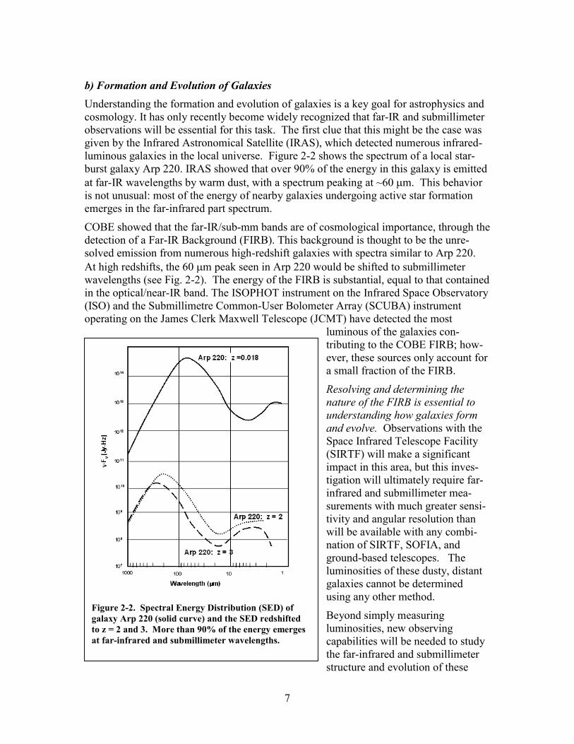
b) Formation and Evolution of GalaxiesUnderstanding the formation and evolution of galaxies is a key goal for astrophysics andcosmology. It has only recently become widely recognized that far-IR and submillimeterobservations will be essential for this task. The first clue that this might be the case wasgiven by the Infrared Astronomical Satellite (IRAS), which detected numerous infrared-luminous galaxies in the local universe. Figure 2-2 shows the spectrum of a local star-burst galaxy Arp 220. IRAS showed that over 90% of the energy in this galaxy is emittedat far-IR wavelengths by warm dust, with a spectrum peaking at ~60 �m. This behavioris not unusual: most of the energy of nearby galaxies undergoing active star formationemerges in the far-infrared part spectrum.
COBE showed that the far-IR/sub-mm bands are of cosmological importance, through thedetection of a Far-IR Background (FIRB). This background is thought to be the unre-solved emission from numerous high-redshift galaxies with spectra similar to Arp 220.At high redshifts, the 60 �m peak seen in Arp 220 would be shifted to submillimeterwavelengths (see Fig. 2-2). The energy of the FIRB is substantial, equal to that containedin the optical/near-IR band. The ISOPHOT instrument on the Infrared Space Observatory(ISO) and the Submillimetre Common-User Bolometer Array (SCUBA) instrumentoperating on the James Clerk Maxwell Telescope (JCMT) have detected the most
luminous of the galaxies con-tributing to the COBE FIRB; how-ever, these sources only account fora small fraction of the FIRB.
Resolving and determining thenature of the FIRB is essential tounderstanding how galaxies formand evolve. Observations with theSpace Infrared Telescope Facility(SIRTF) will make a significantimpact in this area, but this inves-tigation will ultimately require far-infrared and submillimeter mea-surements with much greater sensi-tivity and angular resolution thanwill be available with any combi-nation of SIRTF, SOFIA, andground-based telescopes. Theluminosities of these dusty, distantgalaxies cannot be determinedusing any other method.
Beyond simply measuringluminosities, new observingcapabilities will be needed to studythe far-infrared and submillimeterstructure and evolution of these
Figure 2-2. Spectral Energy Distribution (SED) ofgalaxy Arp 220 (solid curve) and the SED redshiftedto z = 2 and 3. More than 90% of the energy emergesat far-infrared and submillimeter wavelengths.

8
galaxies. What are the roles of star formation and active nuclei in the creation of thisluminosity? How do these roles change with time?
Progress has been made both observationally and theoretically in understanding the starformation rate in galaxies. However, there is still significant difficulty in reconciling theestimates for the star formation rate given by ultraviolet, visible, infrared, and submilli-meter observations. For instance, Figure 2-3 (Blain et al. 2002) shows estimates of thestar formation rate of the universe as a function of redshift determined at a variety ofwavelengths. There is a dramatic increase in the star formation rate at redshifts greaterthan ~0.4. However, these data do not yet constrain the redshift at which the starformation rate begins to decline; for instance, z~5 is not ruled out. The interpretation ofthe optical and near infrared data suffers from large and uncertain corrections for dustextinction. The existing submillimeter data are difficult to interpret, since the number ofobjects is small, and few redshifts are known. Furthermore, it is not yet clear what theconnection is, if any, between the high redshift star-forming galaxies seen in the opticaland near infrared and those seen in the submillimeter.
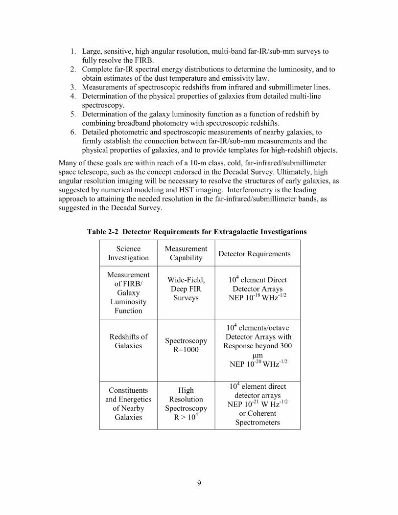
It is clear that much more detailed information will be required in order to fullyunderstand early galaxy formation and evolution, and the nature of the far-infraredbackground. Some of the key observations will include:
Figure 2-3: Estimated history of star formation rate per unit commoving volume inthe universe (from Blain et al 2002). The individual points represent various opticaland near-infrared measurements, and the single up-pointing arrow representscurrent submm estimates. The thick solid and dashed curves represent best fits of asimple luminosity evolution model and a hierarchical model of luminous merginggalaxies to the far-infrared and submillimeter data. Further details of the plot canbe found in Blain et al. (2002).
9
1. Large, sensitive, high angular resolution, multi-band far-IR/sub-mm surveys tofully resolve the FIRB.
2. Complete far-IR spectral energy distributions to determine the luminosity, and toobtain estimates of the dust temperature and emissivity law.
3. Measurements of spectroscopic redshifts from infrared and submillimeter lines.4. Determination of the physical properties of galaxies from detailed multi-line
spectroscopy.5. Determination of the galaxy luminosity function as a function of redshift by
combining broadband photometry with spectroscopic redshifts.6. Detailed photometric and spectroscopic measurements of nearby galaxies, to
firmly establish the connection between far-IR/sub-mm measurements and thephysical properties of galaxies, and to provide templates for high-redshift objects.
Many of these goals are within reach of a 10-m class, cold, far-infrared/submillimeterspace telescope, such as the concept endorsed in the Decadal Survey. Ultimately, highangular resolution imaging will be necessary to resolve the structures of early galaxies, assuggested by numerical modeling and HST imaging. Interferometry is the leadingapproach to attaining the needed resolution in the far-infrared/submillimeter bands, assuggested in the Decadal Survey.
Table 2-2 Detector Requirements for Extragalactic Investigations
ScienceInvestigation
MeasurementCapability Detector Requirements
Measurementof FIRB/Galaxy
LuminosityFunction
Wide-Field,Deep FIRSurveys
104 element DirectDetector Arrays
NEP 10-18 WHz-1/2
Redshifts ofGalaxies Spectroscopy
R=1000
104 elements/octave Detector Arrays withResponse beyond 300
�m NEP 10-20 WHz-1/2
Constituentsand Energetics
of NearbyGalaxies
HighResolution
SpectroscopyR > 104
104 element directdetector arrays
NEP 10-21 W Hz-1/2
or CoherentSpectrometers

10
c) Formation of Stars and PlanetsAlthough the general outlines of the star formation process are known, many of the mostimportant aspects remain elusive. What initiates the core collapse? How are binary starsformed? What is the detailed role of disks to outflows from protostars? What determinesthe mass of a star? What processes determine when, where and how planets form, andwith what masses? Far-infrared and submillimeter observations are critical for the studyof star and planet formation for three fundamental reasons. First, since star formationregions are cold, they radiate predominantly at long wavelengths. To understand thephysical processes acting during star formation, we must observe the dominant form ofradiated energy. Second, the process of conversion of interstellar clouds into starsinvariably occurs in regions of high dust extinction. Stars are born in cold interstellarcloud cores that are so optically thick they are sometimes undetectable even in the mid-infrared. Far-infrared and submillimeter photons can penetrate this dust and allow thestudy of the underlying objects and processes. Third, the dominant atomic and molecularspectral lines that provide cooling in these clouds are at infrared and submillimeter wave-lengths. Additionally, the chemical evolution of star forming regions is best explored atthese wavelengths where the spectra show an amazing richness of features (see, forexample, Figure 2-5). These spectral signatures have great diagnostic potential forunraveling the physical, dynamical andchemical evolution of clouds.
Key to addressing these questions will be theimproved angular resolution promised byfuture large missions at wavelengthsinaccessible from the ground. While SIRTFand Herschel will be yield substantialinformation on the long-wavelength emissionfrom these regions, neither facility will havethe angular resolution to explore the keyphysical scales of the star formation process.A new generation of far-infrared andsubmillimeter missions will improve on thesituation. A far-infrared 10-m telescope, forexample, provides a resolution of ~1 arcsec at50�m (~ 100 AU for the nearest star formingregions), so imaging could probe the densityand temperature structure of these ~1000 AUcollapsing cores on critical physical scales(Figure 2-4). This angular resolution willbegin to allow the investigation of frag-mentation and binary star formation. High-resolution far-infrared and submillimeterspectroscopy with a large FIR telescope wouldenable study of the dynamical collapse ofdense cores on these angular scales, providinga velocity resolution better than 1 km/s.
Figure 2-4. HH-30 disk and jet observedwith HST/WFPC-2. The circle indicatesthe resolution attainable at 50 �m with a10-m FIR telescope. (C. Burrows, K.Stapelfeldt, the WFPC2 Science Team, andNASA).
11
In addition to observing structures associated with disks, an understanding of the starformation process will need studies of entire star formation complexes. The regions ofinterest range from a few arcminutes to nearly a degree across, and maps in bothcontinuum emission from the dust as well as maps in important emission lines will beneeded to assess the physical conditions in the clouds. The requirement for efficientmapping at high resolution requires that facilities be equipped with very large formatarrays of far-infrared and submillimeter detectors. Spectroscopic investigations of starforming regions will also greatly benefit from large detector arrays. With SOFIA, forexample, large format far infrared arrays would be needed for the construction of a crossdispersed echelle spectrograph that would give spatially resolved spectra of extendedstructures.
Ultimately, very high angular resolution observations will be crucial to confirmingtheories outlining how stars form and interact with their surrounding disk environment,and in understanding exactly what factors control whether and how planets form.Resolutions of 0.1 to 1 AU are required to probe circumstellar disk structure in theregions of terrestrial planet formation, searching for disk gaps and measuring the sharpthermal and compositional gradients that are predicted as a consequence of planetgrowth. Core accretion and outflow processes can be studied, and the structure near theinterface between the central star and disk can be probed. These resolutions will be
attainable with a 1 to 10 km baselineinterferometer at 50�m for thenearest star formation regions.
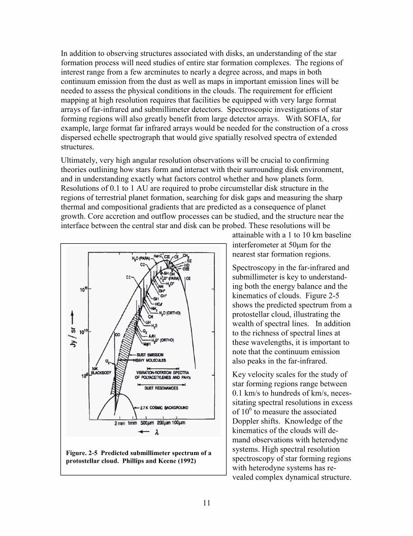
Spectroscopy in the far-infrared andsubmillimeter is key to understand-ing both the energy balance and thekinematics of clouds. Figure 2-5shows the predicted spectrum from aprotostellar cloud, illustrating thewealth of spectral lines. In additionto the richness of spectral lines atthese wavelengths, it is important tonote that the continuum emissionalso peaks in the far-infrared.
Key velocity scales for the study ofstar forming regions range between0.1 km/s to hundreds of km/s, neces-sitating spectral resolutions in excessof 106 to measure the associatedDoppler shifts. Knowledge of thekinematics of the clouds will de-mand observations with heterodynesystems. High spectral resolutionspectroscopy of star forming regionswith heterodyne systems has re-vealed complex dynamical structure.
Figure. 2-5 Predicted submillimeter spectrum of aprotostellar cloud. Phillips and Keene (1992)

12
Figure 2-6 shows spectra that were taken with SWAS that illustrate the richness of thekinematic information available with these types of observations. By combining the highangular resolution with the kinematic information possible with heterodyne receivers, itwill be possible to produce detailed dynamical models of representative systems.
The technical challenges for future detector development for spectroscopy are twofold.First, high performance systems need to be pushed to beyond 1 THz since many of thelines occur at � < 300 �m. Second, exploration of the structure of these regions willrequire mapping over extended regions, and arrays of heterodyne receivers will berequired for observing efficiency.
Table 2-3. Detector Needs for Star Formation Investigations
ScienceInvestigation
MeasurementCapability
DetectorRequirements
Census of StarFormation
Regions/ Structureof Young StellarObjects (YSO’s)
High ResolutionContinuumMapping
104 element Detector Arrays at Far Infrared and
Submillimeterwavelengths
Cloud and YSOKinematics andEnergy Balance
High resolutionSpectroscopy
R>106
Arrays of CoherentReceivers and/or Arrays of
Direct Detectors
Figure 2-6 SWAS spectra of the 557 GHz transition of ortho-H2O in various star formationregions showing the wide variety of line shapes. Ashby et al (2000).
13
III. Detector Overview
In this section we describe fundamental limits to detector performance, summarize thecurrent state of the art, and present our findings for the developments in detectors anddetector systems needed to answer the key science questions identified in the NASAStrategic Plans and the National Academy of Sciences reports.
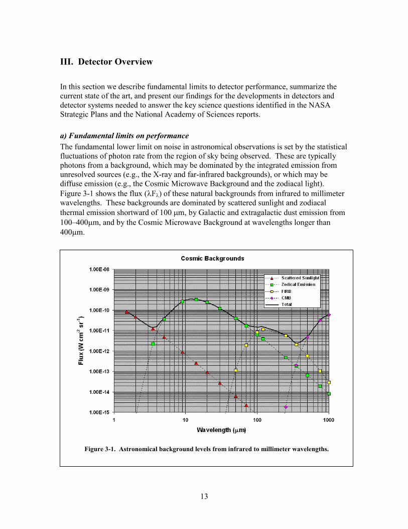
a) Fundamental limits on performanceThe fundamental lower limit on noise in astronomical observations is set by the statisticalfluctuations of photon rate from the region of sky being observed. These are typicallyphotons from a background, which may be dominated by the integrated emission fromunresolved sources (e.g., the X-ray and far-infrared backgrounds), or which may bediffuse emission (e.g., the Cosmic Microwave Background and the zodiacal light).Figure 3-1 shows the flux (�F�) of these natural backgrounds from infrared to millimeterwavelengths. These backgrounds are dominated by scattered sunlight and zodiacalthermal emission shortward of 100 �m, by Galactic and extragalactic dust emission from100–400�m, and by the Cosmic Microwave Background at wavelengths longer than400�m.
Figure 3-1. Astronomical background levels from infrared to millimeter wavelengths.
14
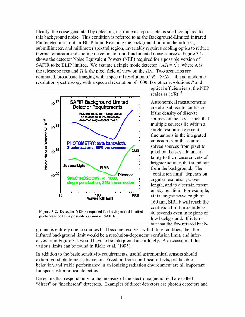
Ideally, the noise generated by detectors, instruments, optics, etc. is small compared tothis background noise. This condition is referred to as the Background-Limited InfraredPhotodetection limit, or BLIP limit. Reaching the background limit in the infrared,submillimeter, and millimeter spectral region, invariably requires cooling optics to reducethermal emission and cooling detectors to limit fundamental noise sources. Figure 3-2shows the detector Noise Equivalent Powers (NEP) required for a possible version ofSAFIR to be BLIP limited. We assume a single mode detector (A� = �2), where A isthe telescope area and � is the pixel field of view on the sky. Two scenarios arecomputed, broadband imaging with a spectral resolution of R = ���� = 4, and moderateresolution spectroscopy with a spectral resolution of 1000. For other resolutions R and
optical efficiencies �, the NEPscales as (�/R)1/2.
Astronomical measurementsare also subject to confusion.If the density of discretesources on the sky is such thatmultiple sources lie within asingle resolution element,fluctuations in the integratedemission from these unre-solved sources from pixel topixel on the sky add uncer-tainty to the measurements ofbrighter sources that stand outfrom the background. The“confusion limit” depends onangular resolution, wave-length, and to a certain extenton sky position. For example,at its longest wavelength of160 �m, SIRTF will reach theconfusion limit in as little as40 seconds even in regions oflow background. If it turnsout that the far-infrared back-
ground is entirely due to sources that become resolved with future facilities, then theinfrared background limit would be a resolution-dependent confusion limit, and infer-ences from Figure 3-2 would have to be interpreted accordingly. A discussion of thevarious limits can be found in Rieke et al. (1995).
In addition to the basic sensitivity requirements, useful astronomical sensors shouldexhibit good photometric behavior. Freedom from non-linear effects, predictablebehavior, and stable performance in an ionizing radiation environment are all importantfor space astronomical detectors.
Detectors that respond only to the intensity of the electromagnetic field are called“direct” or “incoherent” detectors. Examples of direct detectors are photon detectors and
Figure 3-2. Detector NEP's required for background-limitedperformance for a possible version of SAFIR.
15
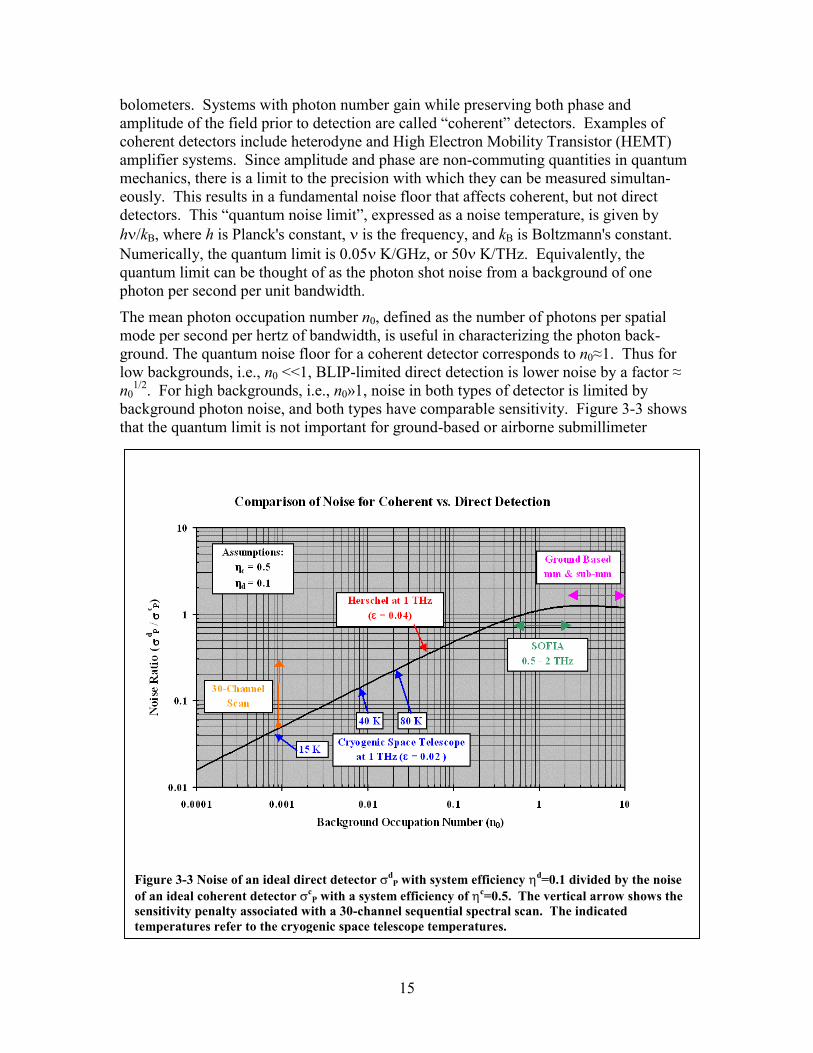
bolometers. Systems with photon number gain while preserving both phase andamplitude of the field prior to detection are called “coherent” detectors. Examples ofcoherent detectors include heterodyne and High Electron Mobility Transistor (HEMT)amplifier systems. Since amplitude and phase are non-commuting quantities in quantummechanics, there is a limit to the precision with which they can be measured simultan-eously. This results in a fundamental noise floor that affects coherent, but not directdetectors. This “quantum noise limit”, expressed as a noise temperature, is given byh�/kB, where h is Planck's constant, � is the frequency, and kB is Boltzmann's constant.Numerically, the quantum limit is 0.05� K/GHz, or 50� K/THz. Equivalently, thequantum limit can be thought of as the photon shot noise from a background of onephoton per second per unit bandwidth.
The mean photon occupation number n0, defined as the number of photons per spatialmode per second per hertz of bandwidth, is useful in characterizing the photon back-ground. The quantum noise floor for a coherent detector corresponds to n0≈1. Thus forlow backgrounds, i.e., n0 <<1, BLIP-limited direct detection is lower noise by a factor ≈n0
1/2. For high backgrounds, i.e., n0»1, noise in both types of detector is limited bybackground photon noise, and both types have comparable sensitivity. Figure 3-3 showsthat the quantum limit is not important for ground-based or airborne submillimeter
Figure 3-3 Noise of an ideal direct detector �dP with system efficiency �d=0.1 divided by the noise
of an ideal coherent detector �cP with a system efficiency of �c=0.5. The vertical arrow shows the
sensitivity penalty associated with a 30-channel sequential spectral scan. The indicatedtemperatures refer to the cryogenic space telescope temperatures.

16
telescopes where the background is dominated by hot thermal emission of the optics orthe atmosphere, but is a serious issue at frequencies beyond 1 THz for a cold telescope inspace, where direct detectors enjoy a large advantage. As a result, direct detection shouldbe used for imaging instruments and low-to-medium resolution spectroscopy on low-background space telescopes. Note, however, that the CMB itself contributes n0>1 belowabout 50GHz (� = 6 mm); thus at these frequencies, coherent receivers can becompetitive for observation of the CMB.
The situation for high-resolution spectroscopy is subtler. While grating spectrometerswith array detectors are the systems of choice for moderate resolutions, they cannotprovide the highest resolutions at long wavelengths. The difficulty with grating spec-trometers is that for a resolution R, the linear size must be of order R�. Achieving R =106 at � = 200 µm would require a cold grating 200 meters long! Other classes ofspectrometer, such as Fabry–Perot spectrometers, solve this size problem by folding theoptical path, and resolutions approaching R = 106 are achievable. The cost is reducedsensitivity because of the need to scan through the spectrum. Fig. 3-3 shows the penaltyfor a scan of 30 spectral elements, which is sufficient to give a modest amount ofinformation about the line shape. In practice, system factors combine to strongly favorcoherent heterodyne detection for high-resolution spectroscopy for frequencies below1.5–2THz (� >200 - 150 �m). In addition, coherent detection is competitive at lowfrequencies where quantum noise is not an issue.
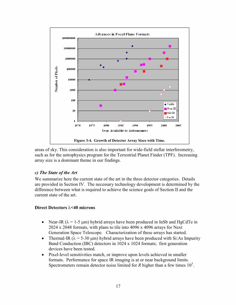
b) Detector ArraysAstronomy has greatly benefited from the advances in semiconductor technology overthe past few decades. Following the original observation by Moore (1965) that thecomplexity of integrated circuits was doubling on a yearly basis, the industry has main-tained an exponential rate of growth for more than 40 years. The array sizes available toastronomy have shown a similar growth. Figure 3-4 shows the increase in formats overthe years. The advantages of large format arrays have been well documented, and theyinclude greatly increased efficiency, sensitivity, ability to accurately assess backgrounds,high precision photometry, and high precision positional information. Clearly, however,the longest wavelengths have yet to realize the full potential of large array formats.
The time required to measure a given section of sky to a specified noise level scales asSensitivity2 / Npixels. The squared dependence gives a high priority to improvements indetector sensitivity. However, the detection sensitivity for astronomical sources willeventually be limited by background photon noise or confusion. In that case, increasingthe number of pixels becomes the highest priority of detector development. Forbroadband imaging applications, the raw sensitivity of existing long wavelength directdetectors is adequate to approach background or confusion limits. Large gains inobserving capability will need to come primarily from increasing array sizes. Opticalarrays are now in use with tens of millions of pixels. In contrast, the largest far-infraredarray is the 32x32 SIRTF photoconductor array. The situation is the same across theentire wavelength range that we are considering. To answer the fundamental sciencequestions discussed in Section II, significantly larger far infrared and submillimeterarrays will be needed. Since the angular resolution of future missions will likely be anorder of magnitude better than SIRTF, much larger arrays will be needed to cover useful
17
areas of sky. This consideration is also important for wide-field stellar interferometry,such as for the astrophysics program for the Terrestrial Planet Finder (TPF). Increasingarray size is a dominant theme in our findings.
c) The State of the ArtWe summarize here the current state of the art in the three detector categories. Detailsare provided in Section IV. The necessary technology development is determined by thedifference between what is required to achieve the science goals of Section II and thecurrent state of the art.
Direct Detectors �<40 microns
� Near-IR (� = 1-5 �m) hybrid arrays have been produced in InSb and HgCdTe in2024 x 2048 formats, with plans to tile into 4096 x 4096 arrays for NextGeneration Space Telescope. Characterization of these arrays has started.
� Thermal-IR (� = 5-30 �m) hybrid arrays have been produced with Si:As ImpurityBand Conduction (IBC) detectors in 1024 x 1024 formats; first generationdevices have been tested.
� Pixel-level sensitivities match, or improve upon levels achieved in smallerformats. Performance for space IR imaging is at or near background limits.Spectrometers remain detector noise limited for R higher than a few times 103.
Figure 3-4. Growth of Detector Array Sizes with Time.

18
� Extrinsic silicon (especially Si:Sb) technology has only limited support outside ofNASA and is therefore vulnerable. The associated silicon readout technology fortemperatures below 20 K is not firmly established.
� Industry is a key partner in this wavelength range, and astronomy-relevanttechnologies need to be sustained to assure they are available.
Direct Detectors � > 40 micron� No military or commercial technology is available for long wavelength direct
detectors.� Flight Ge:Ga photoconductor arrays for SIRTF have 1024 pixels at 70µm, and 40
pixels at 160 µm, with MOS multiplexers.� Work on IBC detectors from Ge or GaAs may improve pixel performance and
extend lithographed photon detector arrays to ~ 400 µm, but significant effort willbe needed to demonstrate useful performance for even a single pixel.
� Concepts for longer wavelength superconducting photon detectors have beendemonstrated and ideas exist for multiplexers.
� Semiconducting bolometer arrays up to several hundred pixels are in use or underdevelopment, but it will be difficult to scale JFET amplifier technology to largerarrays. Larger arrays using MOSFET readouts are under development for theHerschel mission.
� Superconducting TES bolometers with SQUID amplifiers have demonstratedexcellent test results from individual pixels. Lithographed arrays of bothabsorber-coupled bolometers and antenna-coupled bolometers with integratedfilters are being fabricated. Output multiplexing has been demonstrated.
Coherent Detectors� Mixers operate at nearly the quantum noise limit for frequencies below ~500 GHz
(� = 600 �m) but performance degrades to 20 - 40 times the quantum limit above1 THz (� = 300 �m).
� A number of local oscillator (LO) technologies are in use, including frequencymultipliers, lasers, and vacuum tube devices.
� Only small mixer arrays have been built.� The best present amplifier performance is roughly 3 times the quantum limit
below 10 GHz (� = 30 mm) and 6 times the limit at 100 GHz (� = 3 mm). Thehighest amplifier frequency is above 200 GHz (� = 1.5 mm).
� Amplifier arrays of 10 - 20 elements have been built
19
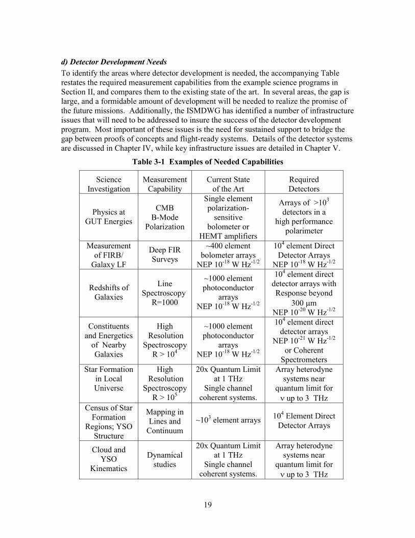
d) Detector Development NeedsTo identify the areas where detector development is needed, the accompanying Tablerestates the required measurement capabilities from the example science programs inSection II, and compares them to the existing state of the art. In several areas, the gap islarge, and a formidable amount of development will be needed to realize the promise ofthe future missions. Additionally, the ISMDWG has identified a number of infrastructureissues that will need to be addressed to insure the success of the detector developmentprogram. Most important of these issues is the need for sustained support to bridge thegap between proofs of concepts and flight-ready systems. Details of the detector systemsare discussed in Chapter IV, while key infrastructure issues are detailed in Chapter V.
Table 3-1 Examples of Needed Capabilities
ScienceInvestigation
MeasurementCapability
Current Stateof the Art
RequiredDetectors
Physics atGUT Energies
CMBB-Mode
Polarization
Single elementpolarization-
sensitivebolometer or
HEMT amplifiers
Arrays of >103
detectors in ahigh performance
polarimeter
Measurementof FIRB/
Galaxy LF
Deep FIRSurveys
~400 elementbolometer arrays
NEP 10-18 W Hz-1/2
104 element DirectDetector Arrays
NEP 10-18 W Hz-1/2
Redshifts ofGalaxies
LineSpectroscopy
R=1000
~1000 elementphotoconductor
arraysNEP 10-18 W Hz-1/2
104 element directdetector arrays withResponse beyond
300 �mNEP 10-20 W Hz-1/2
Constituentsand Energetics
of NearbyGalaxies
High Resolution
SpectroscopyR > 104
~1000 elementphotoconductor
arraysNEP 10-18 W Hz-1/2
104 element directdetector arrays
NEP 10-21 W Hz-1/2
or CoherentSpectrometers
Star Formationin LocalUniverse
High Resolution
SpectroscopyR > 105
20x Quantum Limitat 1 THz
Single channelcoherent systems.
Array heterodynesystems near
quantum limit for� up to 3 THz
Census of StarFormation
Regions; YSOStructure
Mapping inLines and
Continuum~103 element arrays 104 Element Direct
Detector Arrays
Cloud andYSO
Kinematics
Dynamicalstudies
20x Quantum Limitat 1 THz
Single channelcoherent systems.
Array heterodynesystems near
quantum limit for� up to 3 THz
20
e) Principal Findings
Far-infrared and Submillimeter ArraysAs its most important conclusion, the ISMDWG finds that an aggressive effort to developthe largest possible format far-infrared and submillimeter detector arrays would be themost significant benefit to the NASA Space Science Program in the area of infrared,submillimeter, and millimeter detectors. Arrays of 103-104 pixels will be needed forSOFIA and the important future mission concepts. For spectroscopy, sensitivityimprovements of two orders of magnitude are needed. It is essential that completeprototype systems be fabricated. Because of the wide range of applications for thesearrays, it is likely that a variety of technologies will be needed to satisfy the differentrequirements.
We strongly support the development of large format bolometer arrays, in particular TESsystems. These will likely be an essential element of the far-infrared to millimeter wave-length astronomy program. In particular, the development of complete systems,including sensors, readouts, cryogenic systems, and electronics, will be needed to meetthe ambitious science goals of NASA.
We encourage continued work toward very large photoconductor arrays. In particular,the realization of Impurity Band Conduction detectors that operate at far-infrared andsubmillimeter wavelengths should be pursued. Promising new material systems such asGaAs should be explored. Readouts for far-infrared photoconductors need continueddevelopment.
Support for Infrastructure and Intermediate Technology Readiness Level (TRL) DetectorDevelopmentMechanisms, such as the SARA Program, exist within NASA to support low-TRLdevelopments, while mission funding is available for the final development to bringtechnologies to full flight status. As systems become more complex and expensive, themethods to support the work to take promising concepts to mid-TRL prototypes are verylimited. The ISMDWG strongly encourages NASA to develop the resources to supportthis type of engineering, as a complement to the existing SARA program, which shouldretain its role of supporting innovative low-TRL research.
As part of this finding, we encourage NASA to explore methods for supporting keyinfrastructure elements in the research community. There is limited commercial ormilitary interest for most of the technologies discussed in this report, so NASA will haveto assume responsibility for the bulk of the development effort. Often, the work involvesspecialized facilities or equipment, and there are currently very few ways to provide theneeded support. In particular, the push to large array formats will likely requiresubstantial new investments in equipment and facilities.
Improvements in Coherent SystemsFor coherent systems the most important goal is to continue the push toward bettersensitivity. Between frequencies of 1 - 3 THz (� = 300 - 100 �m), the attained sensitivityis well below that set by the quantum limit, and significant improvements are possible.

21
For submillimeter heterodyne receivers, a priority is continued local oscillatordevelopment, where higher frequencies, wider tuning bandwidths, and more outputpower are all important. The development of arrays of coherent receivers will providesignificant improvements in mapping speed.
Readout TechnologyMultiplexing is the key issue for achieving large format arrays.
For TES bolometers, superconducting SQUID readouts provide low-noise, low-poweramplification. Multiplexed SQUID readouts will be essential for the construction of verylarge format bolometer arrays for a CMB polarization mission, and we strongly endorsecontinued development of this technology.
For photoconductive detectors, maintenance of the design and fabrication capabilities forlarge format silicon readout integrated circuits is of vital importance throughout thewavelength range covered by this report. Relative to the costs of integrated circuitdevelopment, the available OSS funding is limited, and the success of producing highperformance cryogenic (T < 20 K) readouts has been spotty. The ISMDWG urges OSSto develop resources to insure the availability of this technology in the future.
Maintenance of Si:Sb Detector CapabilitySi:Sb Blocked Impurity Band detectors are a unique NASA-developed technology.These detectors provide the highest performance detectors in the key 28-40 �mwavelength range. We note that the continued maintenance of this capability is critical toastronomical research in this wavelength band.
Distribution of Surplus Flight DetectorsSurplus detectors from major missions should be made available on a competed basis tothe scientific community for use in other NASA flight programs, SOFIA instruments,ground-based instrumentation, and laboratory testing. We also endorse an examinationof the spares philosophy with the goal of maximum scientific return throughout OSS.
22
IV Detailed Detector Discussion
a) 1 – 40 µm Detector ArraysThe previous decade has seen a dramatic increase in the available sensitivity and formatof various types of multiplexed IR detector arrays within the wavelength range 1 – 40µm. These hybrid arrays have been developed and optimized for space astronomy, and,with appropriate modifications, for higher background ground-based astronomicalapplications. They have been successfully used in a wide range of scientific applications,ranging from relatively broadband imaging to high-resolution spectroscopy. They havebeen used for detailed studies of a wide range of objects and physical processes, rangingfrom extrasolar giant planets, brown dwarfs, proto-planetary disks and star formation, toobscured active galactic nuclei, primeval galaxies and the origins of the first stars andgalaxies. Dust-enshrouded regions, substellar mass temperature ranges, molecular bands,and the UV-optical emission of high-redshift sources are all accessible from spaceplatforms at these wavelengths.
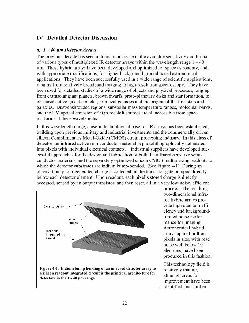
In this wavelength range, a useful technological base for IR arrays has been established,building upon previous military and industrial investments and the commercially drivensilicon Complimentary Metal-Oxide (CMOS) circuit processing industry. In this class ofdetector, an infrared active semiconductor material is photolithographically delineatedinto pixels with individual electrical contacts. Industrial suppliers have developed suc-cessful approaches for the design and fabrication of both the infrared-sensitive semi-conductor materials, and the separately optimized silicon CMOS multiplexing readouts towhich the detector substrates are indium bump-bonded. (See Figure 4-1) During anobservation, photo-generated charge is collected on the transistor gate bumped directlybelow each detector element. Upon readout, each pixel’s stored charge is directlyaccessed, sensed by an output transistor, and then reset, all in a very low-noise, efficient
process. The resultingtwo-dimensional infra-red hybrid arrays pro-vide high quantum effi-ciency and background-limited noise perfor-mance for imaging.Astronomical hybridarrays up to 4 millionpixels in size, with readnoise well below 10electrons, have beenproduced in this fashion.
This technology field isrelatively mature,although areas forimprovement have beenidentified, and further
Figure 4-1. Indium bump bonding of an infrared detector array toa silicon readout integrated circuit is the principal architecture fordetectors in the 1 - 40 �m range.

23
advancements and optimizations are warranted. While a useful industrial base has beenestablished, one must remember that the total astronomical market remains relativelysmall, and that industrial participation and progress is dependent upon sustained funding.
The common astronomical hybrid detector arrays in this region can be grouped by wave-length depending on the energy gap of the infrared active detector material. At the short-est wavelengths (1 - ~5 �m), photovoltaic (PV) detector arrays are used. These diodedetectors are made from intrinsic semiconductors, are typically operated with a modestback bias, and have inherently high absorption efficiency. The most sensitive detectorchoice for applications between 5 and ~40 µm is extrinsic silicon. In this technology, anappropriate impurity is introduced (doped) into the silicon lattice, so that a relativelysmall (long-wavelength) energy gap results to create mobile carriers. Whether the detec-tor substrate is made of intrinsic or extrinsic semiconductor, they are bonded with indiumbumps to a silicon CMOS multiplexer (or ‘readout’) to form a hybrid structure.
Photovoltaic IR Detector ArraysAt the shortest IR wavelengths, 1 to about 5 µm, PV detectors have been fabricated fromintrinsic semiconductor materials such as indium antimonide (InSb, with 5.3 µm cutoff)and mercury cadmium telluride (Hg(1-x)CdxTe, with variable cutoff).
InSb arrays with excellent sensitivity have been developed for SIRTF (256 x 256 format)and the Japanese Astro-F (412 x 512 format). A major development program is under-way for the Next Generation Space Telescope (NGST). Data indicate that the NGSTread noise requirement of <9 electrons read noise (multiply sampled) will be achieved at30 K. Material purity and processing technologies have steadily improved. The physicaldimensions of the detector-grade substrates have increased to about 75 mm, large enoughto accommodate 2048 x 2048 arrays of 25 µm pixels. Ground-based InSb arrays are
commercially available in1024 x 1024 formats, anddevelopmental 2048 x2048 hybrids for ground-based applications havebeen produced and suc-cessfully tested. NGST issponsoring the develop-ment and demonstrationof 2048 x 2048 low-background arrays thatmeet the requirements ofthis mission. Thesecandidate arrays will be‘tiled’ together into 4096x 4096 mosaics and opti-mized for operation at 30K.
HgCdTe arrays have beendeveloped for scientific
Figure 4-2. WFC3 Infrared Focal Plane Array. The detector is a1024x1024 HgCdTe array with a 1.7 �m cutoff.
24
use in a range of alloy compositions (and hence, of cutoff wavelengths and operatingtemperatures). The Near Infrared Camera and Multi-Object Spectrometer (NICMOS)arrays were developed for HST nearly a decade ago, with 2.5 µm-cutoff material in a 256x 256 format. Steady progress has been made, and substantially larger arrays with thiscutoff are now available for ground-based applications. As with InSb, larger detectorsubstrates have been produced to accommodate 2048 x 2048 formats. These arrays havepixel sizes near 18 µm. For space applications, both 1.7 µm-cutoff arrays for Wide FieldCamera 3 (WFC3) and 5 µm-cutoff arrays for NGST are under development, the latter in2048 x 2048 format. Figure 4-2 shows the 1024 x 1024 pixel infrared focal plane arrayfor WFC3 that will be installed on HST in 2004. The 5 µm-cutoff arrays being developedfor NGST, like other modern devices of this type, are produced by molecular beamepitaxy. Test data indicate excellent sensitivity, with correlated double sampled noise of~15 electrons at 35 K; the noise requirements for NGST appear to be achievable. Likethe competing InSb candidate for NGST, HgCdTe detectors will be implemented in tiledarray modules of 4096 x 4096 pixels, which are baselined for operation at 37 K.
These PV detectors utilize silicon CMOS readouts produced at commercial foundries.Because the required operating temperatures are above the carrier freeze out at ~20 K, thereadout circuits can be implemented with reasonably conventional design rules andprocessing steps. Close cooperation between designers within the detector houses, andtheir counterparts at the silicon foundries, is important in developing low-noise, low-power readouts appropriate for astronomical applications. The overall sensitivity ofrecent intrinsic arrays is very good, with quantum efficiencies approaching unity, andread noise, after multiple sampling, well below 10 electrons rms.
Impurity Band Conduction (IBC)� IR Detector ArraysFor longer wavelengths, extrinsic silicon is used as the detector material. Modernextrinsic silicon detectors are now produced with a very thin, very highly-doped detectorlayer, in the IBC (also called BIB) configuration. Figure 4-3 depicts the representativestructure of an n-type IBC detector. The energy band diagram shows the heavily dopedIR absorbing layer with the associated impurity band and the low-doped blocking layerthat prevents the dark current from reaching the electrical contacts. The IBC / BIBdetectors have demonstrated clear advantages in radiation hardness and photometricoperation, and they offer a modest extension in wavelength coverage compared to theearlier bulk photoconductors. The arsenic-doped silicon IBC (Si:As, ~28 µm cutoff) wasthe first, and is the clearly the most mature, example of this class. This material providesuseful spectral coverage down to ~5 µm. It was incorporated in formats of both 128 x128 and 256 x 256 on SIRTF, with operating temperatures around 6 K. Quantumefficiencies above 60%, and multiply sampled read noise at or below 10 electrons, havebeen achieved. A prototype NGST Si:As IBC array with a 1024 x 1024 format has beenproduced and tested. The sensitivity is similar to that achieved in smaller formats. Arelatively new variant of this detector material, antimony-doped silicon (Si:Sb IBC), wasdeveloped for the Infrared Spectrograph on SIRTF, and useful response has been � The terms Impurity Band Conduction (IBC), and the trademarked name Blocked Impurity Band (BIB),are equivalent.

25
achieved out to ~38 µm.These SIRTF arrays, in 128x 128 format, will operate at4 – 5 K, with somewhatlower quantum efficiencyand higher noise. A higher-background version of theseSi:Sb arrays, in 256 x 256format, will fly in theFORCAST instrument onSOFIA. These IBC devicesexhibit excellent photometricbehavior, in many respectsacting like PV detectors.
Since temperatures of 4 - 8K are needed to suppressdark current, specializedlow-temperature readouts arerequired. The siliconmultiplexers must bespecially designed andprocessed, to allow low noise operation at sub-freezeout temperatures. This is a difficultchallenge, both because of the low-temperature device physics, and because of theongoing problem of identifying silicon foundries willing to depart from their normalprocessing schedules. There are numerous examples of such ‘deep-cryo’ customfoundries failing, or moving on to other interests. Years are often required to (try to) re-establish a lost capability, with serious consequences in the development of readouts inboth the 5 – 40 µm range, and also for the 50 – 200+ µm far-infrared, which requireseven lower temperatures.
Promising Directions
Array FormatsThe continued development of ever larger formats can be expected with adequatesupport. Formats of 4096 x 4096 pixels appear to be feasible today. Extending formatsbeyond the NGST objectives should be done with activities that are aligned to futureOrigins and SEU goals.
Detector MaterialsRefinements in modern material growth techniques, in particular those using molecularbeam epitaxy, are resulting in improvements in Hg(1-x)CdxTe. It should be possible toextend the high quantum efficiency and moderate operating temperatures of this materialsystem to significantly longer wavelengths.
Figure 4.3 (a) Representative Structure of n-Type IBC Detector; (b)Band diagram of the detector. (Haller and Beeman 2002).

26
Readout technologyBoth the format and functionality of readout integrated circuits can be improved.Examples include on-chip clock generation, reference pixels, star tracking circuitry, andA/D conversion capability. For mid-IR and longer wavelengths, effort is needed toimprove the custom deep-cryogenic CMOS readouts required to achieve low noise attemperatures below 20 K. The challenge will be to identify ways to take advantage of theincreasingly powerful capabilities of the silicon processing industry while adapting to thefoundries’ commercial emphasis on high-speed digital devices. The potential benefit toNASA would be sophisticated sensor systems that have simple (and low cost) interfacesat the system level.
Developmental technologiesNASA should continue to monitor the status of developments in advanced bandgap-engineered devices such as Quantum Well Infrared Photoconductors (QWIP's), strained-layer superlattice devices, and quantum dots or wires, which may offer improvements inproducibility and higher operating temperature. Some of these technologies promise‘multi-color’ detection (simultaneous detection of photons in 2 or more wavelength bandswithin the same detector), which may have applicability in specific scientific investi-gations. NASA should also monitor advanced energy resolving / photon countingtechnologies such as the Superconducting Tunnel Junctions (STJ) and Transition EdgeSensors (TES), that may be emerging at very near-IR wavelengths. These technologiesshould be supported when technological progress appears encouraging, and thecharacteristics of the devices align well with future OSS mission requirements.
Development Findings
Si:Sb BIB TechnologySi:Sb technology is unique to NASA. It has proven to be useful for application in SIRTFand SOFIA, but is not fully developed. This technology that will be lost unless it issustained by NASA
Array FormatsFuture NASA missions will require improved large format arrays, with excellentsensitivity (high quantum efficiency, low noise, low dark current, and good photometricperformance). It is desirable to develop more highly integrated, on-chip arrayelectronics, so that the interface would involve only a few noise-immune digital (oroptical) lines. It is also desirable to achieve array technologies that operate at highertemperatures without degrading sensitivity. For future large space missions, simplifiedcryogenic systems or passively-cooled approaches may be essential. Silicon readoutelectronics will continue to be critical in achieving these large-format arrays. Thechallenging aspects of deep-cryogenic silicon CMOS processing for multiplexingreadouts are essentially unique to NASA; the techniques and know-how need to besupported and sustained by NASA. It is important to note that many of these readoutconsiderations also apply to long-wavelength photon detectors.
27
b) Long Wavelength Direct Detectors
Direct detectors for wavelengths from 40 µm to several mm are used to measure manydifferent astronomical phenomena including thermal radiation from dust in our galaxy,redshifted dust emission from the earliest galaxies, and the CMB. These sourcescomprise >80% of the radiant energy in the universe. Because there is no commercial ormilitary interest, these detectors are built by and for astronomers. Progress in receiversensitivity has been remarkable. The speed with which a given region of the sky can bemapped has increased by a factor 1018 in 40 years, corresponding to a doubling of speedevery 12 months. Sensitivities of individual detectors are approaching the fundamentallimits set by photon noise. As shown in Figure 3-2, these correspond to NEP ~ 10-18
WHz-1/2 for photometry, which can be achieved, and ~10-20 WHz-1/2 for spectroscopy,which remains difficult. However, the science goals discussed in Section II will requirearrays of long wavelengths direct detectors in formats that do not now exist.
There are many requirements for useful arrays of direct detectors. These includesensitivity at the photon noise limit for the particular application, insensitivity to cosmicrays, wide dynamic range, simple time response, low power dissipation, moderatecryogenic requirements, etc. System requirements such as output multiplexing andpractical ambient electronics are also critical. Existing long wavelength arrays are eitherlimited to a few hundreds of detectors or fall short of the above requirements in importantways. There is much room for improvement. Fortunately, developments now envisionedor now in progress promise to enable the arrays required for future missions. However asustained effort by NASA will be required to produce flight-ready hardware.
There are three main types of long wavelength direct detector. In a photon detector, theabsorbed photon creates one or two electronic excitations that are measured before theyare thermalized. Examples include photovoltaic, photoconductive, and blocked-impurity-band (BIB) devices made from semiconductors. There are also quasiparticle photondetectors made from superconductors. Photon detectors have a long wavelength cut-offset by the excitation energy (energy gap) and an operating temperature requirement set bythe noise from the thermally excited dark current. In thermal detectors, such asbolometers with semiconductor or superconducting Transition Edge Sensor (TES)thermometers, the electronic excitation by the absorbed photon is thermalized before it ismeasured. There is no fundamental long wavelength cut-off, and the operatingtemperature requirement is set by the need to reduce thermal fluctuation noise. Therequired temperatures are typically lower than for photon detectors. A third distinct typeof receiver, used as a direct detector at millimeter wavelengths, consists of a HighElectron Mobility Transistor (HEMT) amplifier followed by a diode direct detector. Thisapproach is subject to the quantum noise limit and is described in Section IVc.

28
Photon DetectorsPhotoconductive detectors of Ge:Ga have been widely used for astronomy, for example,on IRAS, COBE, IRTS, ISO, and the Kuiper Airborne Observatory. Ge:Ga arrays havebeen developed for the Multiband Imaging Photometer for SIRTF (MIPS) instrument,and detectors are being developed for spectroscopy with the Photoconductor ArrayCamera and Spectrometer (PACS) instrument on Herschel. The MIPS has two Ge:Gaarrays. One array has 1024 unstressed detectors covering 50-100 �m. The other arrayhas 40 detectors, which have been stressed to reduce the excitation energy, for a 160 µmband. They operate at temperatures of 1.5 K, have detective quantum efficiencies of 15-20%, and use custom (but commercially produced) cryogenic CMOS charge-integratingamplifiers and multiplexers. The SIRTF arrays are the result of a long developmentprocess and are a major achievement. The 70µm array (Figure 4-4) is the only 1024-element far-infrared direct detector system. There is, however, room for improvement.Higher quantum efficiencies would yield significant benefits. Conventional germaniumphotoconductors have low absorption coefficients, require large volumes, and thus havesignificant cosmic ray sensitivity. They also have complicated time responses that affectcalibration, observing strategies and data analysis in low background applications.Recent theoretical insight suggests that there may be an opportunity to eliminate some ofthe nonlinear behavior. Compared to the hybrid detector arrays found at shorter wave-lengths, these arrays are complex and require hand assembly of monolithic elements. Inparticular, in the case of stressed detectors, the need to apply a uniaxial stress to extendthe long wavelength cutoff adds significant mechanical complexity.
At shorter wavelengths, silicon photoconductors have been replaced by IBC (or BIB)devices that have anumber of well-known advantages.These include highquantum efficiency,low cosmic raycross-section,simple timeresponse, extendedwavelength cover-age, and arrayfabrication by opti-cal lithography. Amodest NASA pro-gram to producelonger wavelengthIBC detectors fromGe has made steadyprogress. How-ever, methods forproducing therequired epitaxial
Figure 4-4. The SIRTF/ MIPS Ge:Ga Array. The array is 32x32 formatand covers the wavelength range 50 - 110 �m.

29
low-doped blocking layer remain problematic. Recent successes in producing low-dopedepitaxial blocking layers suitable for GaAs IBC detectors suggests that it may be possibleto extend IBC photon detector performance to arrays at wavelengths as long as 400µm.Satisfactory detector pixels are anticipated, but have not yet been produced. If success-ful, however, the potential payoff will be very large, promising many of the benefitscurrently enjoyed at shorter wavelengths including operating temperatures higher thanrequired by thermal detectors and the applicability of silicon multiplexer technology.MOSFET amplifiers and multiplexers that operate at these low temperatures exist, buttheir use at longer wavelengths will require additional optimization. Additionally, themaintenance of the foundry production capabilities remains an issue.
An entirely different type of photon detector is being developed which use the very smallexcitation energy in a superconductor. In these devices, photons are absorbed in a coldsuperconducting film where the electrons are bound into Cooper pairs. Each incidentphoton breaks a pair and creates two single excited electrons, or quasiparticles. Thereadout is designed to be sensitive to quasiparticles, but not to the pairs. Individual pixelsof two different devices show promising performance and multiplexing schemes havebeen suggested. However, it is too early to judge whether these approaches will extendphoton detection to mm wavelengths.
Thermal DetectorsWell-developed semiconductor bolometer technologies exist to produce arrays of tens tohundreds of pixels that are operated at temperatures of 100 to 300 mK. They aretypically fabricated by lithography on membranes of Si or SiN and use thermistors of ion-implanted silicon or neutron-transmutation-doped Ge. Thermistor impedances of ~ 107 �match well to JFET amplifiers operated at ~ 100K. An AC bias is used when low fre-quency noise must be minimized. The photons are absorbed by metal films that can becontinuous or patterned in a mesh. Thepatterning can be designed to minimize thecosmic ray cross section, to select thespectral band, to provide polarizationsensitivity, or to control the throughput.Bolometer architectures include pop-upstructures or two-layer bump bondedstructures for close-packed arrays and spiderweb or other bolometers for horn-coupledarrays. Bolometers are used from 40 to2000µm in many experiments includingNASA pathfinder ground based instruments,and balloon experiments such asBOOMERANG, MAXIMA and BAM.Figure 4-5 shows a spider web bolometerfrom the BOOMERANG experiment. Thistype of detector is being used on spaceexperiments such as the High FrequencyInstrument (HFI) on Planck and SPIRE on
Figure 4-5. BOOMERANG Spider Web bolometer.
30
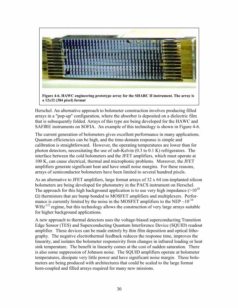
Herschel. An alternative approach to bolometer construction involves producing filledarrays in a "pop-up" configuration, where the absorber is deposited on a dielectric filmthat is subsequently folded. Arrays of this type are being developed for the HAWC andSAFIRE instruments on SOFIA. An example of this technology is shown in Figure 4-6.
The current generation of bolometers gives excellent performance in many applications.Quantum efficiencies can be high, and the time-domain response is simple andcalibration is straightforward. However, the operating temperatures are lower than forphoton detectors, necessitating the use of sub-Kelvin (0.3 to 0.1 K) refrigerators. Theinterface between the cold bolometers and the JFET amplifiers, which must operate at100 K, can cause electrical, thermal and microphonic problems. Moreover, the JFETamplifiers generate significant heat and have small noise margins. For these reasons,arrays of semiconductor bolometers have been limited to several hundred pixels.
As an alternative to JFET amplifiers, large format arrays of 32 x 64 ion-implanted siliconbolometers are being developed for photometry in the PACS instrument on Herschel.The approach for this high background application is to use very high impedance (>1010
�) thermistors that are bump bonded to MOSFET amplifiers and multiplexers. Perfor-mance is currently limited by the noise in the MOSFET amplifiers to the NEP ~10-16
WHz-1/2 regime, but this technology allows the construction of very large arrays suitablefor higher background applications.
A new approach to thermal detectors uses the voltage-biased superconducting TransitionEdge Sensor (TES) and Superconducting Quantum Interference Device (SQUID) readoutamplifier. These devices can be made entirely by thin film deposition and optical litho-graphy. The negative electrothermal feedback reduces the response time, improves thelinearity, and isolates the bolometer responsivity from changes in infrared loading or heatsink temperature. The benefit in linearity comes at the cost of sudden saturation. Thereis also some suppression of Johnson noise. The SQUID amplifiers operate at bolometertemperatures, dissipate very little power and have significant noise margin. These bolo-meters are being produced with architectures that could be scaled to the large formathorn-coupled and filled arrays required for many new missions.
Figure 4-6. HAWC engineering prototype array for the SHARC II instrument. The array isa 12x32 (384 pixel) format
31
In addition, there is work on bolometers that are coupled to the optics by planar litho-graphed antennas and superconducting microstrip transmission lines. In this implemen-tation, the absorbing element is a resistive termination to the line, which can be verysmall. At low operating temperatures (~ 100 mK) such terminations can be depositeddirectly on the dielectric substrate. The weakness of the coupling between electrons andphonons provides adequate thermal isolation between the (hot) electrons and the substratewithout the use of membranes or legs. In antenna-coupled bolometers, the signal ispropagated in a superconducting microstrip transmission line. These lines can branch toform diplexers, and can incorporate high performance microstrip bandpass filters forfrequencies up to ~700 GHz (� ~ 430 �m). It should even be possible to make a low-resolution spectrometer with this technology. This feature may prove important forobtaining photometric redshift information at long wavelengths and for doing directdetection spatial interferometry. However, this development is at an early stage. Theperformance of superconducting antennas, transmission lines and diplexers, has beendemonstrated in other contexts, but their use in bolometer systems has not been fullydemonstrated.
Large format arrays of antenna-coupled TES bolometers or possibly superconductingphoton detectors are very attractive candidates for a CMB polarization mission. Broad-band antennas with RF diplexing and/or interleaved antennas can make efficient use ofthe focal plane. Antennas are inherently polarization sensitive, and the excellent gainstability provided by the feedback in TES bolometers facilitates polarization differencing.Such detectors are necessary for the high frequency bands of a CMB polarization missionand would be sufficient for all bands. However, much work remains to be done on thebolometers themselves and, especially, on the design of a high performance bolometricpolarimeter.
Large format arrays of TES bolometers must have output multiplexing to avoid verylarge numbers of leads leaving the cryostat. Lines of 30-50 detectors can be multiplexedbefore amplification using superconducting thin film technology. A time-domainmultiplexer that uses a SQUID for each bolometer to switch the outputs sequentiallythrough a single SQUID amplifier has been fabricated and successfully demonstrated.Progress is being made on a frequency-domain multiplexer which combines the signalsfrom a row of bolometers, each of which is biased at a different frequency. The signalsare then amplified by a single SQUID and recovered with ambient temperature lock-inamplifiers. The success of TES bolometer arrays ultimately depends on the success ofone or both of these multiplexer technologies.
Individual devices with a variety of architectures have been fabricated by lithography andtested successfully. Fabrication of large format arrays is in progress. However, very littlework has been done on system architectures. Fortunately, the basic building blocks of thetype of system that will be needed for space submillimeter and millimeter missions arecommon both to ground-based long-wavelength systems and to TES X-ray calorimeterson missions such as Constellation X. The NASA long wavelength infrared program canbenefit greatly from these developments if and only if it makes a sustained investment indemonstrating the unique aspects of the systems architectures that will be necessary forinfrared and mm-wave applications. In particular, scaling to 103 –104 pixels will requiresubstantial development beyond the proof-of-principle stage to insure flight-ready status.
32
Summary
PhotoconductorsSemiconducting photon detector arrays of 1024 pixels exist for wavelengths out to 120µm. These arrays use CMOS readout multiplexing technology that has been adaptedfrom shorter wavelengths. Expansion to larger formats while retaining the system leveladvantages that are present with this technology is important. Development of Ge orGaAs IBC detectors, which could improve pixel performance and extend large formatphoton detector array technology to several hundred µm will be of particular importance.Readout issues such as compatibility with very long wavelength detectors and the manu-facturing infrastructure should be addressed.
TES BolometersThe new TES bolometer technology has a number of useful operational characteristics,and should be producible in large format arrays. It is compatible with time domain orfrequency domain multiplexing to SQUID amplifiers. The expectation is that this techno-logy will enable large format detector arrays with very good performance over a widerange of wavelengths. The development of SQUID multiplexers will be critical to thesuccess of TES bolometers. Support should be sought to improve the maturity ofpromising bolometer technologies and to develop the system architectures required forvery large arrays on future missions.
Semiconducting BolometersSemiconducting bolometric detectors with individual JFET amplifiers perform well, andarrays of up to several hundred pixels are under development or in use for manymissions. However, this JFET technology is difficult to scale to large format arrays forspace missions. Large format bolometer arrays mated to MOSFET readouts are beingdeveloped for Herschel, and we recommend that NASA monitor developments in thisarea.
Research and Analysis Program and System DemonstrationsThe long wavelength direct detector community is very creative, and novel devices canbe expected from it. The SARA program plays an essential role in enabling newdevelopments such as the superconducting photon detectors. Promising new devicesshould be developed as their predicted performance warrants. Many of the detectorsbeing developed are entirely new and have not yet been demonstrated in astronomicalinstrument systems. In addition, several of the mission applications will have verydemanding performance specifications. As a result, it will be crucial to gain experiencewith prototype ground-based, balloon-borne, and airborne instruments using thesetechnologies. The ISMDWG is concerned that present grant sizes may be inadequate todevelop the complex, very large array systems that will be needed in the future, and weencourage exploration of new funding mechanisms.

33
c) Technologies For Coherent DetectionA coherent receiver system (Fig. 4-7) usually consists of a local oscillator (LO), whichproduces a monochromatic signal at frequency �LO; a "mixer", which is a nonlineardevice that down-converts the signal collected by the telescope at frequency �s to a lowermicrowave frequency �IF = |�s-�LO|, known as the intermediate frequency (IF); a series ofIF amplifiers; and finally a "backend" spectrometer which produces a spectrum of the IFsignal. This IF spectrum is a replica of the spectrum of the telescope signal. The mixerusually determines the sensitivity of the system. At submillimeter and far-infraredwavelengths, the mixer is usually a superconducting device. Alternatively, at centimeterand millimeter wavelengths, low-noise amplifiers may be used prior to downconversionusing standard semiconductor diode mixers. For continuum radiometers, such as thoseused for CMB observations, the down-conversion step may be omitted, in which case theamplified signal is filtered and detected, usually with a diode detector. In all cases, thesystem has a large photon number gain, and is therefore subject to the quantum limit.
MixersDramatic advances have been made in submillimeter and far-infrared mixers over thepast decade. Semiconductor Schottky-diode mixers have been replaced bySuperconductor-Insulator-Superconductor (SIS) tunnel junction and superconducting HotElectron Bolometer (HEB) mixers. These devices use metallic low-Tc superconductorsand generally operate at 1.5 - 4 K. Alternative devices are also being investigated, such
telescope
Local Oscillator
IF ampbackend spectrometers
ν
IF
LO
νSν IF system and
multiplier
or MMICGunn osc.
amplifier
mixer
Figure 4-7. Block diagram of a heterodyne spectrometer. The telescope signal is combined witha local oscillator in a mixer, to yield the intermediate frequency

34
as those using semiconductor quantum wells. These may offer advantages such as highertemperature operation, but competitive devices have not yet been demonstrated. SISmixers have achieved sensitivities within a factor of 2 of the quantum limit at millimeterwavelengths. However, mixer performance above 1 THz (�=300 �m) degrades totypically 40 times the quantum limit. It is not yet clear whether current device conceptswill allow the quantum limit to be approached at these higher frequencies, or whethernew ideas will be needed.
SIS MixersAt frequencies below 1.2 THz (� > 250 �m) superconducting tunnel junction(Superconductor-Insulator-Superconductor or SIS) mixers offer the best performance.These devices behave essentially as photodiodes; photon-assisted tunneling produces oneelectron of current per photon absorbed. The tunnel junction itself is usually made usingniobium (Tc = 9.2 K) or higher Tc niobium alloys such as NbN or NbTiN, along with avery thin (10—20 Å) tunnel barrier, usually aluminum oxide or aluminum nitride (AlN).It is nontrivial to fabricate high quality tunnel junctions, and only certain materialscombinations have proved successful. The submillimeter signal is coupled to the SISjunction from a waveguide probe or planar antenna using a thin-film transmission linecircuit. The theory of SIS mixers is quite well developed and is used extensively fordetailed design. One of the main challenges for high-frequency SIS mixer design isdealing with the large parallel-plate capacitance of the SIS junction. It is necessary tofabricate an inductive tuning circuit along with the tunnel junction. This approach is veryeffective for millimeter-wavelength mixers, and noise within a factor of a few of thequantum limit has been achieved. At higher frequencies, especially over 1 THz (� = 300�m), the losses in the tuning circuit become important and cause the mixer performanceto deteriorate. Nevertheless,good performance has beenobtained up to 1.2 THz (� =250 �m) for the HIFIinstrument for the HerschelSpace Observatory, withnoise within a factor of 20of the quantum limit. Theupper frequency limit forSIS mixers given currenttechnology is around 1.5-1.6 THz (� =200-188 �m).
HEB MixersHot Electron Bolometer(HEB) mixers use a small,thin superconducting filmoperating at the transitiontemperature, coupled to awaveguide probe or planar
Figure 4-8 Microbridge HEB mixer designed to operate at frequenciesas high as 2.5 THz. (JPL).
35
antenna. Changes in the submillimeter power deposited in the HEB cause changes in theresistance, much like the TES readouts for direct-detection bolometers. A major issue forHEB mixers is achieving a thermal time constant that is fast enough to yield a useful IFoutput bandwidth of a few GHz. Two methods are used: (1) phonon cooling, using ultra-thin NbN or NbTiN films; (2) diffusion cooling, using sub-micron Nb, Ta, NbAu, or Aldevices coupled to normal-metal cooling “pads” or electrodes. Competitive sensitivitieshave been demonstrated for both types of devices. Phonon-cooled devices perhaps enjoya modest sensitivity advantage, while diffusion-cooled devices may have broader IFbandwidths. In contrast to SIS mixers, HEB devices do not have an identifiable highfrequency limit, and have been demonstrated well into the far-infrared, at frequenciesexceeding 2.5 THz (� ~ 120 �m). Typical performance levels are a factor of 40 over thequantum limit, or roughly 1 K/GHz for the double-sideband noise temperature. Thedetailed physics of HEB mixers is not thoroughly understood yet, although significantprogress is being made.
Local OscillatorsSuperconducting mixers typically require microwatt LO powers, which is roughly 3-4orders of magnitude lower than their semiconductor (Schottky diode) predecessors. As aresult, a broader range of LO sources can be used. The technologies being used orinvestigated include diode multipliers, lasers and optoelectronics, and “vacuum tube”oscillators such as klystrons, including novel nano-fabricated versions.
Frequency MultipliersMultipliers use semiconductor (Schottky varactor) diodes to generate successiveharmonics of a powerful millimeter-wavelength signal. Several multipliers may becascaded to obtain high multiplication factors, e.g. x12 or x16. Dramatic advances in thisarea have been made over the past few years, particularly as a result of the developmentsfor HIFI/Herschel. These advances have come through a combination of sophisticatedelectromagnetic modeling, a better understanding of the device physics, and vastlyimproved device and waveguide fabrication techniques. One major advance has been thedevelopment of millimeter-wave InP HEMT power amplifiers which drive the first stagemultiplier. These amplifiers replace Gunn oscillators, and allow broadband operationwith purely electronic tuning. Another major advance is the development of integrateddiode multipliers, which eliminate the delicate whisker contacts used previously. Thesediode devices are mounted in waveguide blocks, with a waveguide horn output on thefinal stage. This all solid-state approach offers continuous tuning, high reliability, andrelatively straightforward system integration. On the other hand, this approach becomesincreasingly difficult at higher frequencies. At present, useful power from all-solid-statesources has been demonstrated to ~1.5 THz (� = 200 �m).
Lasers and Optoelectronic ApproachesOptically-pumped far-infrared gas lasers can generate > 1 mW power levels and havebeen used in receiver systems, particularly for pumping Schottky-diode mixers, but arenot continuously tunable and have numerous drawbacks for space applications.Semiconductor “quantum-cascade” lasers have recently been demonstrated at 4.4 THz
36
(70 �m), which need only DC current to produce a far-infrared output. So far only pulsed(not CW) operation has been demonstrated. Alternative approaches are being proposed,in which a far-infrared semiconductor laser is pumped using another laser, such as near-infrared diode lasers. Photomixer LO's are another approach for generatingsubmillimeter radiation using optical or near-infrared diode lasers. The photomixer isessentially a very fast detector, and generates the submillimeter beat frequency betweentwo optical or near-IR diode lasers. A very appealing aspect of this approach is thepossibility of generating frequencies over a very wide tuning bandwidth. Whilesubstantial (mW) power levels have been demonstrated at millimeter wavelengths, theoutput power of photomixers drops very rapidly with frequency. Nonetheless, microwattpower levels useful for pumping HEB mixers may be feasible up to 2-3 THz (� = 150 -100 �m).
Vacuum-tube devicesScaled versions of traditional microwave oscillators such as klystrons and backward-wave oscillators have been pushed to frequencies exceeding 1 THz (� = 300 �m). Whilethese devices are continuously tunable, they are often bulky, power hungry, require watercooling, and have limited operating lifetimes, and therefore have limited applicability forspace missions. However, interest in these devices has resurfaced recently, due to novelmicro- and nano-fabrication techniques that may mitigate some of the problems.
AmplifiersLow-noise amplifiers are useful for microwave and millimeter-wave detection,particularly for CMB studies. Substantial performance gains have been achieved throughthe development of cryogenic InP-based HEMT devices and integrated circuits. HEMTamplifiers are also used as the IF amplifiers which follow superconducting mixers in sub-mm heterodyne systems. HEMT's may also find an important role in direct detectionsystems, and are being proposed as preamplifiers for several novel superconductingdetector concepts.
Low-noise Millimeter AmplifiersOver the last decade, two developments in transistor technology have producedsignificant reductions in noise and dissipated power and have enabled operation atfrequencies above 200 GHz (� = 150 �m). The first development was High ElectronMobility Transistors (HEMT's) based on indium phosphide substrates. This developmentwas funded initially by the DOD, and is supported by substantial commercial demand.The second development was Monolithic Microwave Integrated Circuit (MMIC)technology, also supported by large military and commercial demand.
InP amplifiers have achieved excellent noise performance. Cooling from roomtemperature to 20 K lowers noise by roughly an order of magnitude, and noise of threetimes the quantum limit at 8 GHz (� = 38 mm) and six times the quantum limit at 100GHz (� = 3 mm), with nearly uniform performance over bandwidths of 20-30% has beenrealized. Noise and power dissipation are roughly a factor of three lower than in GaAsdevices. Compared to SIS mixers and bolometers, which require temperatures from

37
several K to tenths of a K, InP amplifiers have modest cooling requirements. However,the typical power dissipation is several milliwatts per amplifier, which becomes animportant issue for large arrays.
At frequencies above ~40 GHz (� = 7.5 mm), the performance of MMIC amplifiers isclearly superior to that of amplifiers built from discrete transistors. MMIC amplifiersalso can be assembled much more quickly, and are very reproducible.
The largest millimeter arrays built to date involve several tens of radiometers (i.e.,“pixels”). If this technology is used on a CMB polarization mission, much larger arraysof up to 103 elements would be required. This scale should be achievable with thedevelopment of advanced packaging and manufacturing techniques.
Improvements of amplifier noise by a factor of two are expected with devices based onInSb materials. Currently under development by the DoD, InSb devices also offer theprospect of higher frequency operation and lower power dissipation. Noise of three timesthe quantum limit or lower should be achievable through 100 GHz (�=3 mm) over thenext few years.
IF AmplifiersHIFI/Herschel, along with many other projects, has chosen an IF band of 4-8 GHz.Amplifier performance in this band is truly impressive, with noise temperatures of ~2 K,as low as 3 times the quantum limit. However, broader IF bandwidths are desirable. Anamplifier that operates between 4-12 GHz has been demonstrated, and a 6-18 GHzcryogenic MMIC amplifier is under development.
Spectrometer BackendsA wide variety of technologies are available for backend spectrometers. The majorparameters of interest are bandwidth, spectral resolution, power dissipation, and in somecases, cost. Digital correlators can provide very high spectral resolution (<< 1 MHz), canhave bandwidths of 1-2 GHz per unit, can have numerous operating modes with varyingresolutions and bandwidths, and are straightforward to mass-produce. This technologycontinues to advance rapidly, due to the large investments being made by the semi-conductor industry. However, the power dissipation remains relatively high. Acousto-optic spectrometers (AOS), such as those being developed for HIFI/Herschel, usesubstantially less power and can provide ~1 MHz resolution with four 1 GHz bands in asingle unit. This technology is relatively mature, and only evolutionary improvementsmay be expected. Very wide contiguous bandwidths (4 GHz) with moderate spectralresolution (~30 MHz) can be provided with analog correlators, which have relatively lowpower dissipation. It appears possible to extend this technology to much wider band-widths. An alternative technique for wide band (10-20 GHz) spectroscopy has beenproposed, involving optical modulation of a visible or near-IR laser.
38
Development Priorities
Improvements in SensitivityThe most important goal is to continue the push toward better sensitivity. Sensitivitieswithin a factor of a few of the quantum limit have been achieved below ~500 GHz (� =600 �m ), but there remains much room for improvement throughout the radio to far-infrared spectrum. The need is particularly acute at frequencies between 1-3 THz (�=300- 100 �m), and also at millimeter wavelengths for CMB work. Modern design tools,improved understanding of the device physics, better fabrication techniques, and newmaterials, or better knowledge of materials parameters, will all play important roles.However, in some cases better engineering may not be the answer, and novel deviceconcepts may be needed.
Local OscillatorsFor submillimeter heterodyne receivers, the second priority is continued local oscillatordevelopment. Higher frequencies, wider tuning bandwidths, and more output power areall important. Diode multipliers are the best solution at this point, but may be overtakenby new technologies, especially at the higher frequencies.
Array TechnologyArray receivers allow fast mapping. For CMB measurements, large array receivers arethe second priority for development, since LO’s are not needed. For submillimeterspectroscopy, array receivers are a third priority.
Other issuesBackend spectrometers should be developed in parallel with the receiver front ends. Thegoals here include broad bandwidths, low power, low mass, high spectral resolution, andstable operation.
Power dissipation is obviously a key issue for large arrays of HEMT amplifiers; asubstantial reduction in the dissipated power would be a big benefit.
Increasing the IF and RF bandwidth of heterodyne receivers is important, since thisreduces system complexity and increases the speed of line surveys. Another area toinvestigate is the integration of the final LO stages with the mixer, which would simplifysystem integration.

39
V. Keys to SuccessThere are three major drivers for detector development: 1) support of planned majorNASA missions such as SOFIA and NGST, 2) maintenance and advancement oftechnology for competed missions in the Small Explorer (SMEX) and Medium-ClassExplorer (MIDEX) programs, and 3) development of new technologies that could openup new opportunities for science either through competed missions or future strategicmissions. Each of these efforts has different requirements for implementation.
Major MissionsMajor missions require early development of key detector technologies to keep them offthe critical path. A good example of the benefit of this approach is SIRTF, where theprogram obtained focal planes that met or exceeded the original requirements throughconcentrated efforts on detectors for each instrument. This was possible because ofadequate funding by the project and an intimate knowledge of the system requirementson the part of the instrument teams. NGST is proceeding in a similar fashion but with theproject overseeing the technology development. For major missions, a coordinated,focused early detector development program overseen by the project and/or instrumentteams is essential.
Competed MissionsBoth the Explorer and Discovery programs allow for focused missions to target specific,compelling science questions. Competed missions make efficient use of existing detectortechnology, typically leveraging developments made by large missions. These programsdo not have the budget or schedule for significant detector development. Examples ofcompeted missions that leveraged technology from SIRTF and NGST include the Wide-field Infrared Explorer (WIRE), a SMEX mission, and two MIDEX missions recentlyaccepted for Phase A study, the Next Generation Sky Survey (NGSS) and theAstroBiology Explorer (ABE). NASA must maintain and enhance detectors that havebeen developed for specific missions since this technology is the linchpin that enables theExplorer and Discovery lines to succeed with new, exciting science.
Maintaining Existing CapabilitiesThere is already evidence of the disappearance of capabilities with the completion of theSIRTF focal planes, and such a problem is expected once NGST has completed itsdetector procurement. The cost of maintaining a core group and doing a “developmentcycle” in an industrial vendor type environment (either corporate or at a government lab)ranges from $400 K/year to more than $1 M/year depending on the vendor and the scopeof the effort. This amount is significantly more than a typical ROSS award, but can behighly leveraged due to other programs. It is very important to provide a mechanism forcompetitively funding proposals that maintain or advance key capabilities that arejustified by potential science missions.
40
Program ManagementMaintaining technology requires the continued support of industrial and universitylaboratories. The difficulty that arises is determining which technologies should bemaintained, especially given limited resources. Although peer review is necessary toselect amongst competing proposals, it does not have a long-term corporate memory andcannot provide vision for the program. The ISMDWG believes that a detector “czar” isneeded to see that the overall program is balanced and sustained. Support of key detectortechnologies requires consistent management oversight that looks at the long-term goalsto insure continuity of support.
SOFIAAn important source of support for the infrared, submillimeter, and millimeter detectorcommunity is the SOFIA project. During operations, SOFIA management hopes tospend significant resources on detector development through peer reviewed grants. Withits decades-long lifetime coupled with the ability to quickly change instruments, SOFIAwill be an ideal testbed for advanced detector concepts. Because these detectors willpotentially benefit future space flight missions, there is clear synergy between the SOFIAdetector efforts and other NASA programs. The ISMDWG is encouraged by theexpression of support for detector development by the SOFIA project. We also endorseapplication or leveraging of other NASA technology funding to SOFIA detector needs.
Surplus DetectorsMost major missions produce a surplus of detectors during their development stage.These residual assets can help maintain a knowledge base of this technology in thecommunity and can provide an opportunity for innovative scientific use. They could beused to accomplish exciting science in SMEX and MIDEX missions or ground basedinstruments. This mechanism is not to be used as a substitute for ongoing detector devel-opment, but rather is a way to take full advantage of the technological investment fromflight programs. Making residual detectors available to the community can act as abridge between major missions, and it can keep some of the infrastructure and expertiseavailable for competed missions. Surplus detectors from major missions should be madeavailable on a competed basis to the scientific community for use in the other NASAprograms, ground based instrumentation, and laboratory testing, and would represent anextremely effective use of these government investments.
Mid-TRL DevelopmentIt is clear that sustained investment in future infrared, submillimeter, and millimeterdetector development will be required to assure that the expert teams remain intact, atNASA, in industry, at universities, and within the user community. NASA shouldconsider instituting and managing a detector development program which takes a long-term, strategic view of needs as system develop through the Technology ReadinessLevels (TRL) (see Appendix B). Low TRL development properly occurs through theSpace Astrophysics Research and Analysis (SARA) program, while support for detailedengineering development is available through flight projects. However, mid-TRL (pre-mission) funding is much more difficult to obtain, particularly when there is little

41
commercial or military interest. Bridging this gap is essential if promising technologiesare ever to become candidates for flight. The problem becomes more serious as systemsincrease in complexity, and the needed amount of support exceeds the typical SARAlevels. Alternate funding mechanisms that can support the extension of promisingtechnologies to mid-TRL’s would benefit NASA Space Science efforts.
Detector Fabrication InfrastructureMost of the detector technologies described in this report are of interest only to NASA,and do not have significant commercial or military support. This is especially true foremerging technologies, such as the superconducting detectors. As a result, there arelimited opportunities for leveraging costs, and NASA must largely assume responsibilityfor the entire detector development effort, including the support of the detectorfabrication infrastructure. In particular, new investments in equipment and facilities arelikely to be needed to support the development of large format arrays. Such support isbeyond the scope of the present SARA program.
System-level DemonstrationsMany of the detectors being developed are entirely new and have not yet been demon-strated in astronomical instrument systems. In addition, several of the mission appli-cations such as CMB polarization and submillimeter direct-detection spectroscopy willhave very demanding performance specifications. As a result, it will be crucial to gainexperience with prototype ground-based, balloon-borne, and airborne instruments usingthese new technologies. We encourage NASA to maintain and enhance opportunities toconduct these system-level demonstrations.

42
ReferencesAstronomy and Astrophysics Survey Committee, Board on Physics and Astronomy,
Space Studies Board, National Research Council, 2001, Astronomy andAstrophysics in the New Millennium, National Academy Press: Washington, DC. [Decadal Survey]
Ashby, M. L. N., Bergin, E.A., Plume, R., Carpenter, J., Neufeld, D.A., Chin, Erickson,N. R., Goldsmith, P. F., Harwit, M., Howe, J.E., Kleiner, S. C., Koch, D.G., Patten,B. M., Schieder, R., Snell, R.L., Stauffer, J.R., Tolls, V., Wang, Z., Winnewisser, G.,Zhang, Y.F., and Melnick, G.J. 2000, ApJL, 539, L115.
Blain, A. W., I. Smail, R. J. Ivison, J.-P. Kneib, and D. T. Frayer . 2002, “SubmillimeterGalaxies”, Phys. Rep., in press.
Committee on the Physics of the Universe, M. Turner, Chair, 2002, Connecting Quarkswith the Cosmos: Eleven Science Questions for the New Century, NationalAcademy Press: Washington, DC
Haller, E.E., and Beeman, J. 2002, “Far-Infrared Photoconductors: Recent Advances andFuture Prospects”, Proc. Monterey Workshop on FIR, SubMM, and MM Detectors,NASA/CP-211408.
Hu,W., and Dodelson, S. 2002, "Cosmic Microwave Background Anisotropies", Ann.Rev. Astron. and Astrophys.,
Moore, G. 1965. "Cramming More Components onto Integrated Circuits", Electronics,Vol. 38, April 19, 1965.
Phillips, T. and Keene, J. 1992, "Submillimeter Astronomy", IEEE, Proceedings, vol. 80,no. 11, p. 1662-1678
Rieke, G.H., Young, E.T., and Gautier, T.N.. 1995, “Detection Limits in the Far-Infrared”, Space Science Reviews, 74, 17.

43
Appendix A. Acronyms2MASS Two-Micron All Sky Survey
ABE AstroBiology Explorer
A/D Analog to Digital
AOS Acousto-Optic Spectrometer
ASO Astronomical Search for Origins
BAM Balloon Anisotropy Measurement
BIB Blocked Impurity Band
BLIP Background Limited Infrared Photodetection
BOOMERANG Bolometric Observations Of Millimetric Extragalactic RadiationANd Geophysics
CDS Correlated Double Sample
CMB Cosmic Microwave Background
CMBPol Cosmic Microwave Background Polarization Mission
CMOS Complimentary Metal Oxide Semiconductor
COBE Cosmic Background Explorer
CW Carrier Wave
DoD Department of Defense
DMR Diffuse Microwave Radiometer (on COBE)
DQE Detective Quantum Efficiency
FET Field Effect Transistor
FIR Far-Infrared ( 40 - ~200 �m)
FIRAS Far Infrared Absolute Spectrometer (on COBE)
FIRB Far Infrared Background
GUT Grand Unified Theory
HAWC High-resolution Airborne Widebandwidth Camera
HEB Hot Electron Bolometer
HEMT High Electron Mobility Transistor
HIFI Heterodyne Instrument for the Far-Infrared (on Herschel)
HFI High Frequency Instrument (on Planck)
HST Hubble Space Telescope
IBC Impurity Band Conduction

44
IF Intermediate Frequency
IRAC Infrared Array Camera (on SIRTF)
IRAS Infrared Astronomical Satellite
IRS Infrared Spectrograph (on SIRTF)
IRTS Infrared Telescope in Space
ISMDWG Infrared, Submillimeter, and Millimeter Detector Working Group
ISO Infrared Space Observatory
ISOCAM ISO Camera
ISOPHOT ISO Photo-polarimeter
JCMT James Clerk Maxwell Telescope
JFET Junction Field Effect Transistor
KAO Kuiper Airborne Observatory
LO Local Oscillator
MAXIMA Millimeter Anisotropy eXperiment IMaging Array
MIDEX Medium-class Explorer
MIPS Multiband Imaging Photometer for SIRTF
MIR Mid-Infrared ( 5 - 40 �m )
MMIC Monolithic Microwave Integrated Circuit
MOSFET Metal Oxide Semiconductor Field Effect Transistor
NEP Noise Equivalent Power
NGSS Next Generation Sky Survey
NGST Next Generation Space Telescope
NICMOS Near Infrared Camera Multi Object Spectrometer (on HST)
NIR Near-Infrared ( 1 - 5 �m )
NRAO National Radio Astronomy Observatory
OSS Office of Space Science
PACS Photoconductor Array Camera and Spectrometer (on Herschel)
PC PhotoConductive
PV PhotoVoltaic
QE Quantum Efficiency
QWIP Quantum Well Infrared Photoconductor
RF Radio Frequency

45
ROSS Research Opportunities in Space Science
SAFIR Single Aperture Far Infrared Telescope
SAFIRE Submillimeter and Far Infrared Experiment (on SOFIA)
SARA Space Astronomy Research and Analysis
SCUBA Submillimetre Common-User Bolometer Array
SED Spectral Energy Distribution
SHARC Submillimeter High Angular Resolution Camera
SEU Structure and Evolution of the Universe
SIN Superconducting-Insulator-Normal
SIRTF Space Infrared Telescope Facility
SIS Superconductor-Insulator-Superconductor
SMEX Small Explorer
SOFIA Stratospheric Observatory for Infrared Astronomy
SPIRE Spectral and Photometric Imaging REceiver (on Herschel)
SQUID Superconducting Quantum Interference Device
SSAC Space Science Advisory Committee
SSE Space Science Enterprise
STJ Superconducting Tunnel Junction
Sub-mm Submillimeter (200 to ~1000 �m)
TES Transition Edge Sensor.
TPF Terrestrial Planet Finder
TRL Technology Readiness Level
WFC3 Wide Field Camera 3 (on Hubble Space Telescope)
WIRE Wide Field Infrared Explorer
YSO Young Stellar Object
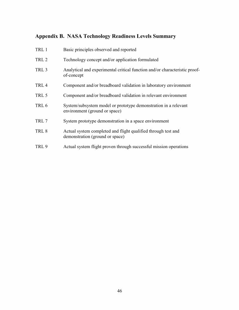
46
Appendix B. NASA Technology Readiness Levels Summary
TRL 1 Basic principles observed and reported
TRL 2 Technology concept and/or application formulated
TRL 3 Analytical and experimental critical function and/or characteristic proof-of-concept
TRL 4 Component and/or breadboard validation in laboratory environment
TRL 5 Component and/or breadboard validation in relevant environment
TRL 6 System/subsystem model or prototype demonstration in a relevantenvironment (ground or space)
TRL 7 System prototype demonstration in a space environment
TRL 8 Actual system completed and flight qualified through test anddemonstration (ground or space)
TRL 9 Actual system flight proven through successful mission operations