designcon 2012 - full system channel co …...designcon 2012 full system channel co-optimization for...
TRANSCRIPT

DesignCon 2012
Full System Channel Co-optimization for 28Gb/s SerDes FPGA Applications with Stacked Silicon Interconnect Technology Namhoon Kim, Xilinx, Inc. [email protected], (408) 879-3563 Zhaoyin Daniel Wu, Xilinx, Inc. [email protected], (408) 879-7722 Jack Carrel, Xilinx, Inc. [email protected], (972) 246-0239 Joong-ho Kim, Xilinx, Inc. [email protected], (408) 879-6117 Paul Wu, Xilinx, Inc. [email protected], (408) 626-6435
Abstract To enable 28 Gb/s transceiver operation, Xilinx has employed many innovative techniques for circuits, packaging and systems. Virtex®-7 HT FPGAs are designed to use Stacked Silicon Interconnect (SSI) technology that relies on an interposer built on low loss package substrate material. Channel loss, reflection loss and crosstalk noise are critical factors in determining system performance at this very high speed. The new concept of SSI in an FPGA device will be introduced. The interposer includes a significant number of TSVs (Through Silicon Vias) for the high speed signals. Technology requirements and manufacturing processes to support 28Gb/s SerDes application will be presented. It is imperative that the signal path including the interposer is accurately modeled over the high frequency operating range by considering all those requirements before design optimization. Detailed design optimization for the interposer has been performed to find optimum design rules by taking into consideration manufacturability and parasitic effects of the TSV’s from DC to high frequency, which can cause major performance degradation. We will also introduce a package design methodology for 28Gb/s SerDes signal support. The package material selection to minimize dielectric loss and trace design to minimize copper/surface roughness loss for the package substrate is very important. In addition, the design topologies to minimize signal loss, reflection loss and crosstalk will be presented. Package and PCB design co-optimization is very important to minimize reflections from solder ball interface. Any single mismatch in the very high speed system can result in the significant closure of the eye diagram. Once full channel analysis has been performed including the optimized silicon interposer model on top of a low loss package substrate and PCB model, the simulation data is then compared to the measured 28Gb/s eye diagram, showing very good correlation. The proposed optimized channel system enables high performance signaling and great visibility of 28Gb/s SerDes enabled FPGA products.
Author(s) Biography Namhoon Kim is a Senior Staff Signal Integrity Engineer in the Advanced Package Design and Development group at Xilinx, Inc., responsible for package development, electrical design/analysis and methodology development for Xilinx FPGA products and systems. Before he joined Xilinx, he worked for Rambus, Inc. and Silicon Image, Inc. He has over 10 years of experience in high speed device and channel design, SI/PI simulation, modeling and characterization of Fibre Channel, SATA, PCIe, DVI/HDMI, DDR and XDR/TBI(12.8Gbps~16Gbps) memory system. He received his BSEE & MSEE degree in Electrical Engineering from KAIST. He is also an IEEE senior member, actively working for major IEEE conferences and societies. He has over 25 published papers and 5 patents in the field of signal and power integrity. Zhaoyin Daniel Wu is a Staff Design Engineer in the SerDes Technology Group at Xilinx, Inc. He is working on SerDes channel modeling/architecture with 3D-IC, EM design/modeling of spiral inductor, finger capacitor (MOMcap), LC-tank, and substrate noise. He was with Ansoft, AltraBroadband Inc., and ITRI before joining Xilinx. He has experience on both RFIC circuit and passive component designs such as UHF RFID Tag (860 ~ 960 MHz), UWB Transceiver (3.1 ~ 4.8 GHz), GSM900/1800, On-Chip Spiral/ Transformer/Balun, Multilayered LTCC/Organic RF Filter, Planar Antenna, and etc. He has 5 published papers in the area of circuit design, and 2 US patent being filed for spiral inductor. Jack Carrel is an applications engineer at Xilinx. He has over 30 years of experience in product development and design in the fields of Instrumentation, Test and Measurement, and Telecommunications. His background includes development of electro-optic modules, Multi-gigabit transceiver boards, high speed and high resolution data acquisition systems for government and commercial applications. Most recently he has been involved in product development and application using multi-gigabit transceivers with specific focus on PCB design issues. He has been published in several professional publications. Jack received his Bachelor of Science degree in Electrical Engineering from the University of Oklahoma. Joong-Ho Kim received his Ph. D. degrees in electrical and computer engineering from Georgia Institute of Technology, Atlanta, Georgia, in 2002. During his graduate study, he developed transmission matrix and macro-modeling methods for analyzing large and complex power delivery networks. In 2011, Joong-Ho joined in Xilinx Inc., San Jose, CA as a Principal Engineer/Technical Director in the Advanced Package Design and Development Department. He is currently working on package/system development, electrical design, analysis, and methodology development for Xilinx FPGA products. During 2005 – 2011, he was working on Technology Development Division, at Rambus Inc., Santa Clara, CA. He was responsible for product/technology design and analysis in signal/power integrity (SI/PI) area for high performance memory interface products such as XDR1/2, DDR2/3/4, GDDR, Mobile XDR, LPDDR2/3, and next generation mobile, computing, and graphic memory systems. During 2002-2005, he worked on SI/PI
analysis for CMOS microprocessors and in-house tool developments at Intel Corp. He is an IEEE senior member, actively working for major IEEE conferences and societies in the semi-conductor area. He has more than fifty publications in refereed journals and conferences, two books (as a chapter author for IEC: Power Distribution Network Design Methodologies, Prentice Hall: High-Speed Signaling: Jitter Modeling, Analysis, and Budgeting), nine issued patents and three patents pending. He received Best Paper Award at EPEP ’00, 1st Place Poster Award at NSF-PRC’ 00, and Best Paper Award at Intel DTTC’ 04, and two Best Paper Awards at IEC DesignCon ’08. Paul Wu is currently with Xilinx as Director of packaging design and signal integrity development. He holds 22 patents and has authored 15 original technical papers. Prior to Xilinx he had been with Prolinx Labs, Intel Corp., Cadence and MCC. Paul earned his BSEE from National Taiwan University and MSEE & Ph.D. in Computer Science from Northwestern University, where he conducted research on discrete and geometric algorithms. His current interests are focusing on development of high density interconnect technologies and design verification methodologies and their applications in advanced semiconductor packaging.

Introduction: World’s First Single-FPGA Solution for 400G Communication To address the insatiable demand for more bandwidth, the telecommunications industry is accelerating development of Nx100G and 400G line cards for communication systems. These systems will leverage new optical interconnect standards to address power density and thermal management issues attendant with scaling the capacity of existing infrastructure. A critical component of the solution is 28 Gb/s electrical interfaces that increase port density and reduce power per bit. Xilinx is responding to the demand for more bandwidth with two key developments. The first is high-fidelity 28 Gb/s transceiver technology that meets the stringent requirements of next-generation communication systems. The second is 28 nm Virtex®-7 HT FPGAs that integrate an unprecedented 16 x 28 Gb/s and 72 x 13.1 Gb/s transceivers with logic, memory, and I/O resources that enable the first silicon device (FPGA or otherwise) to support 400G line cards and the industry’s largest single-FPGA solution for Nx100G line cards. The CEI-28G specification guiding the development of 28G networking imposes extremely tight jitter budgets (0.30 UI) on system designers building 28G chip-to-optics interfaces. Xilinx® GTZ 28 Gb/s transceivers are designed to deliver superior jitter performance. This begins with the phase-locked loop (PLL), which is based on an LC tank design. To ensure maximum design flexibility along with best jitter performance, Virtex-7 HT FPGAs employ a modular, multirate transceiver architecture that provides improved noise immunity. Unique clocking, clock distribution, and PLL design minimizes jitter across multiple transceivers. Additional design features minimize lane-to-lane skew to support tough optical standards like Scalable SerDes Framer Interface (SFI-S) that limit acceptable skew to 500 ps. Creating a single transceiver design that can support line rates spanning the range from 19.6 Gb/s to 28.05 Gb/s while meeting demanding jitter requirements. [1] To enable 28 Gb/s transceiver operation, Xilinx has employed many innovative techniques for circuits and systems. Virtex®-7 HT FPGAs use Stacked Silicon Interconnect (SSI) on the low loss package substrate material. Channel loss, reflection loss and crosstalk noise are critical factors that determine system performance at this very high speed. Any single mismatch in the channel can result in the significant closer of the eye diagram. A system design methodology including the silicon interposer and package that minimizes loss due to attenuation, reflection and crosstalk will be introduced in this paper. Overview of Stacked Silicon Interconnect Technology FPGA-based solutions can provide the system-level functionality currently delivered by ASICs and ASSPs. The requirements for a viable solution include increased capacity, lower power, and higher bandwidth. The most aggressive adopters of FPGA technology are eager to employ the highest capacity and bandwidth device of a new FPGA generation. However, the challenges of building large FPGAs early in the production life cycle can limit the ability to supply the volumes of devices because at the early stages of a new process node, when defect densities are high, die yield declines dramatically as die size increases. To address these issues, Xilinx has introduced stacked silicon interconnect
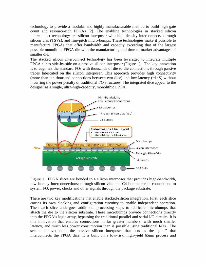
technology to provide a modular and highly manufacturable method to build high gate count and resource-rich FPGAs [2]. The enabling technologies in stacked silicon interconnect technology are silicon interposer with high-density interconnects, through silicon vias (TSVs), and fine-pitch micro-bumps. These technologies make it possible to manufacture FPGAs that offer bandwidth and capacity exceeding that of the largest possible monolithic FPGA die with the manufacturing and time-to-market advantages of smaller die. The stacked silicon interconnect technology has been leveraged to integrate multiple FPGA slices side-by-side on a passive silicon interposer (Figure 1). The key innovation is to augment the standard I/Os with thousands of die-to-die connections through passive traces fabricated on the silicon interposer. This approach provides high connectivity (more than ten thousand connections between two dice) and low latency (~1nS) without incurring the power penalty of traditional I/O structures. The integrated dice appear to the designer as a single, ultra-high-capacity, monolithic FPGA.
Figure 1. FPGA slices are bonded to a silicon interposer that provides high-bandwidth, low-latency interconnections; through-silicon vias and C4 bumps create connections to system I/O, power, clocks and other signals through the package substrate. There are two key modifications that enable stacked-silicon integration. First, each slice carries its own clocking and configuration circuitry to enable independent operation. Then each slice undergoes additional processing steps to fabricate microbumps that attach the die to the silicon substrate. These microbumps provide connections directly into the FPGA’s logic array, bypassing the traditional parallel and serial I/O circuits. It is this innovation that enables connections in far greater numbers, with much smaller latency, and much less power consumption than is possible using traditional I/Os. The second innovation is the passive silicon interposer that acts as the “glue” that interconnects the FPGA dice. It is built on a low-risk, high-yield 65nm process and
provides four layers of metallization for building the traces that connect the logic regions of multiple FPGA slices. The third innovation is the through-silicon vias (TSVs) and C4 solder bumps that mount the FPGA/interposer stack-up on a high-performance package substrate using flip-chip assembly techniques. The coarse-pitch TSVs provide the connections between the package and the FPGA for the parallel and serial I/O, power/ground, clocking, configuration signals, etc. These stacked-silicon FPGAs break through the limitations of monolithic FPGAs, extending their value to create super high capacity FPGAs with unmatched chip-to-chip bandwidth. However, this stack-silicon FPGA approach requires silicon interposer with TSV which does not exist in conventional monolithic FPGAs. Although the silicon interposer is only a hundred micron thick, we need to design it carefully because the conventional TSV design may be a limiting factor in the critical data path due to high capacitive loading and crosstalk caused by a lossy silicon substrate. For high frequency applications like the 28Gb/s SerDes, failure to consider high frequency effects of TSV will degrade the rise/fall time, increase crosstalk, increase noise injection, and cause significant performance degradation of the signal transmitted on a high speed channel.
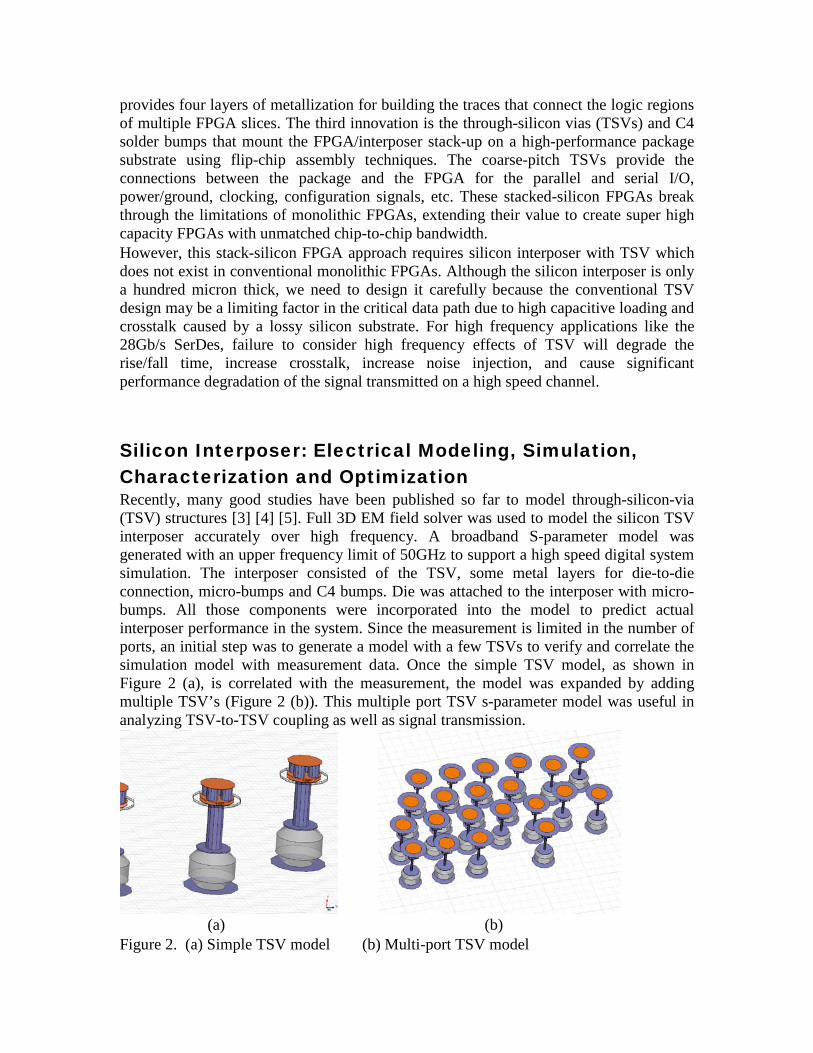
Silicon Interposer: Electrical Modeling, Simulation, Characterization and Optimization Recently, many good studies have been published so far to model through-silicon-via (TSV) structures [3] [4] [5]. Full 3D EM field solver was used to model the silicon TSV interposer accurately over high frequency. A broadband S-parameter model was generated with an upper frequency limit of 50GHz to support a high speed digital system simulation. The interposer consisted of the TSV, some metal layers for die-to-die connection, micro-bumps and C4 bumps. Die was attached to the interposer with micro-bumps. All those components were incorporated into the model to predict actual interposer performance in the system. Since the measurement is limited in the number of ports, an initial step was to generate a model with a few TSVs to verify and correlate the simulation model with measurement data. Once the simple TSV model, as shown in Figure 2 (a), is correlated with the measurement, the model was expanded by adding multiple TSV’s (Figure 2 (b)). This multiple port TSV s-parameter model was useful in analyzing TSV-to-TSV coupling as well as signal transmission.
(a) (b) Figure 2. (a) Simple TSV model (b) Multi-port TSV model
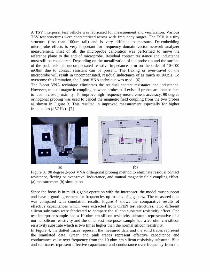
A TSV interposer test vehicle was fabricated for measurement and verification. Various TSV test structures were characterized across wide frequency ranges. The TSV is a tiny structure (less than 100um tall) and is very difficult to measure. De-embedding microprobe effects is very important for frequency domain vector network analyzer measurement. First of all, the microprobe calibration was performed to move the reference plane to the end of microprobe. Residual contact resistance and inductance must still be considered. Depending on the metallization of the probe tip and the surface of the pad, residual, uncompensated resistive impedance term on the order of 10~100 mOhm due to contact resistant can be present. The flexing or over-travel of the microprobe will result in uncompensated, residual inductance of as much as 100pH. To overcome this limitation, the 2-port VNA technique was used. [6] The 2-port VNA technique eliminates the residual contact resistance and inductance. However, mutual magnetic coupling between probes still exists if probes are located face to face in close proximity. To improve high frequency measurement accuracy, 90 degree orthogonal probing was used to cancel the magnetic field coupling from the two probes as shown in Figure 3. This resulted in improved measurement especially for higher frequencies (>5GHz). [7]
(a) (b) Figure 3. 90 degree 2-port VNA orthogonal probing method to eliminate residual contact resistance, flexing or over-travel inductance, and mutual magnetic field coupling effect. (a) measurement (b) simulation Since the focus is in multi-gigabit operation with the interposer, the model must support and have a good agreement for frequencies up to tens of gigahertz. The measured data was compared with simulation results. Figure 4 shows the comparative results of effective capacitances which were extracted from OPEN test structures. Two different silicon substrates were fabricated to compare the silicon substrate resistivity effect. One test interposer sample had a 10 ohm-cm silicon resistivity substrate representative of a normal silicon resistivity and the other test interposer sample had a 20 ohm-cm silicon resistivity substrate which is two times higher than the normal silicon resistivity. In Figure 4, the dotted traces represent the measured data and the solid traces represent the simulated data. Green and pink traces represent effective capacitance and conductance value over frequency from the 10 ohm-cm silicon resistivity substrate. Blue and red traces represent effective capacitance and conductance over frequency from the
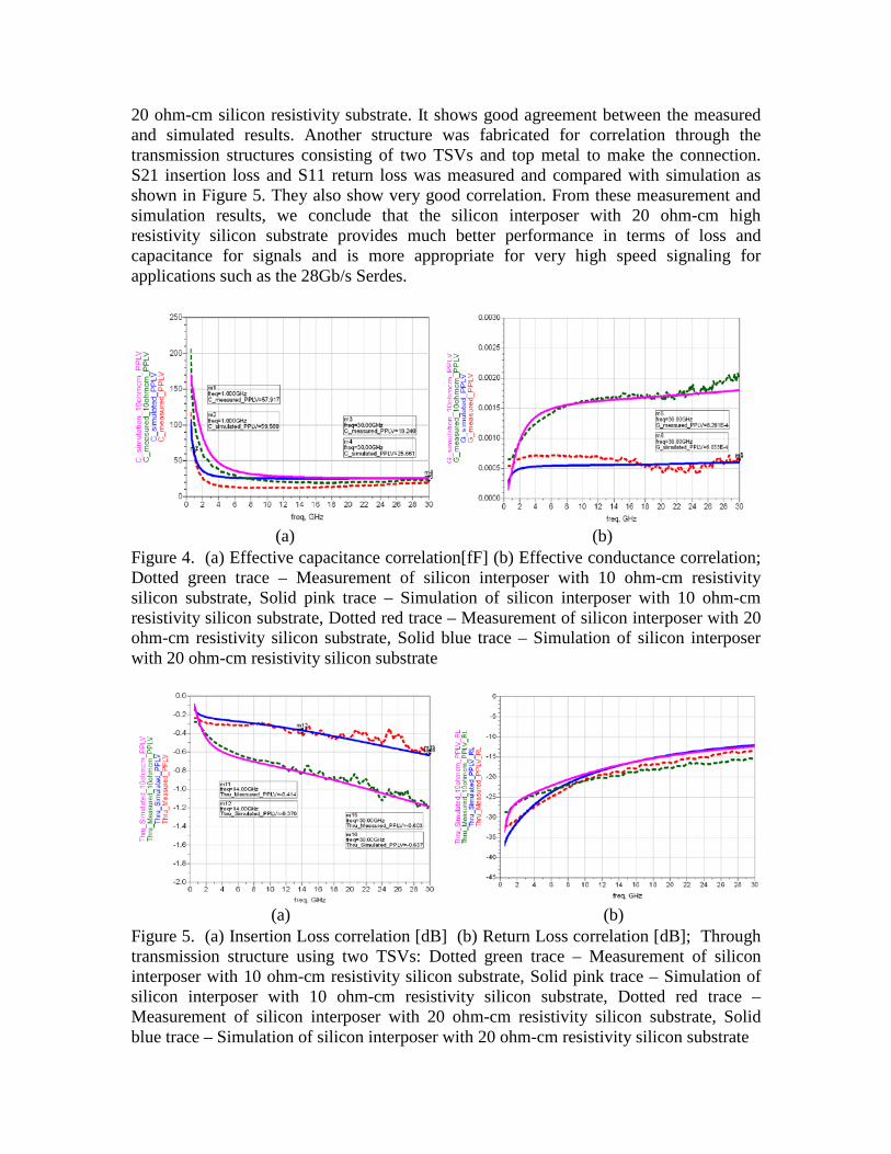
20 ohm-cm silicon resistivity substrate. It shows good agreement between the measured and simulated results. Another structure was fabricated for correlation through the transmission structures consisting of two TSVs and top metal to make the connection. S21 insertion loss and S11 return loss was measured and compared with simulation as shown in Figure 5. They also show very good correlation. From these measurement and simulation results, we conclude that the silicon interposer with 20 ohm-cm high resistivity silicon substrate provides much better performance in terms of loss and capacitance for signals and is more appropriate for very high speed signaling for applications such as the 28Gb/s Serdes.
(a) (b) Figure 4. (a) Effective capacitance correlation[fF] (b) Effective conductance correlation; Dotted green trace – Measurement of silicon interposer with 10 ohm-cm resistivity silicon substrate, Solid pink trace – Simulation of silicon interposer with 10 ohm-cm resistivity silicon substrate, Dotted red trace – Measurement of silicon interposer with 20 ohm-cm resistivity silicon substrate, Solid blue trace – Simulation of silicon interposer with 20 ohm-cm resistivity silicon substrate
(a) (b) Figure 5. (a) Insertion Loss correlation [dB] (b) Return Loss correlation [dB]; Through transmission structure using two TSVs: Dotted green trace – Measurement of silicon interposer with 10 ohm-cm resistivity silicon substrate, Solid pink trace – Simulation of silicon interposer with 10 ohm-cm resistivity silicon substrate, Dotted red trace – Measurement of silicon interposer with 20 ohm-cm resistivity silicon substrate, Solid blue trace – Simulation of silicon interposer with 20 ohm-cm resistivity silicon substrate
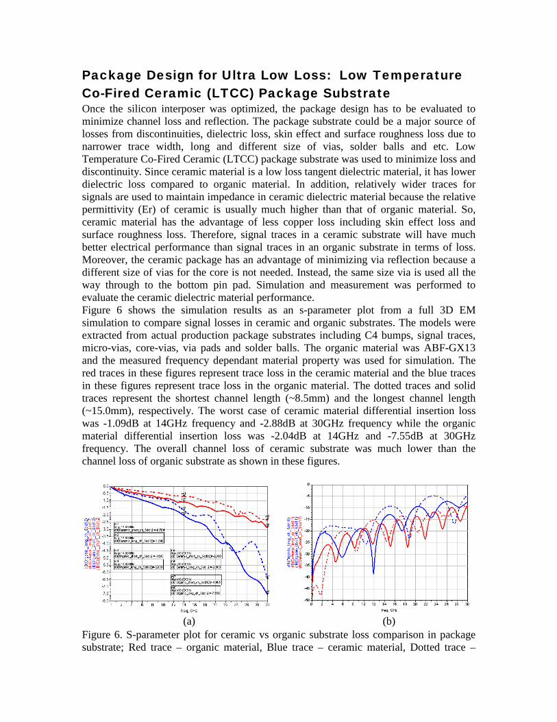
Package Design for Ultra Low Loss: Low Temperature Co-Fired Ceramic (LTCC) Package Substrate Once the silicon interposer was optimized, the package design has to be evaluated to minimize channel loss and reflection. The package substrate could be a major source of losses from discontinuities, dielectric loss, skin effect and surface roughness loss due to narrower trace width, long and different size of vias, solder balls and etc. Low Temperature Co-Fired Ceramic (LTCC) package substrate was used to minimize loss and discontinuity. Since ceramic material is a low loss tangent dielectric material, it has lower dielectric loss compared to organic material. In addition, relatively wider traces for signals are used to maintain impedance in ceramic dielectric material because the relative permittivity (Er) of ceramic is usually much higher than that of organic material. So, ceramic material has the advantage of less copper loss including skin effect loss and surface roughness loss. Therefore, signal traces in a ceramic substrate will have much better electrical performance than signal traces in an organic substrate in terms of loss. Moreover, the ceramic package has an advantage of minimizing via reflection because a different size of vias for the core is not needed. Instead, the same size via is used all the way through to the bottom pin pad. Simulation and measurement was performed to evaluate the ceramic dielectric material performance. Figure 6 shows the simulation results as an s-parameter plot from a full 3D EM simulation to compare signal losses in ceramic and organic substrates. The models were extracted from actual production package substrates including C4 bumps, signal traces, micro-vias, core-vias, via pads and solder balls. The organic material was ABF-GX13 and the measured frequency dependant material property was used for simulation. The red traces in these figures represent trace loss in the ceramic material and the blue traces in these figures represent trace loss in the organic material. The dotted traces and solid traces represent the shortest channel length (~8.5mm) and the longest channel length (~15.0mm), respectively. The worst case of ceramic material differential insertion loss was -1.09dB at 14GHz frequency and -2.88dB at 30GHz frequency while the organic material differential insertion loss was -2.04dB at 14GHz and -7.55dB at 30GHz frequency. The overall channel loss of ceramic substrate was much lower than the channel loss of organic substrate as shown in these figures.
(a) (b) Figure 6. S-parameter plot for ceramic vs organic substrate loss comparison in package substrate; Red trace – organic material, Blue trace – ceramic material, Dotted trace –
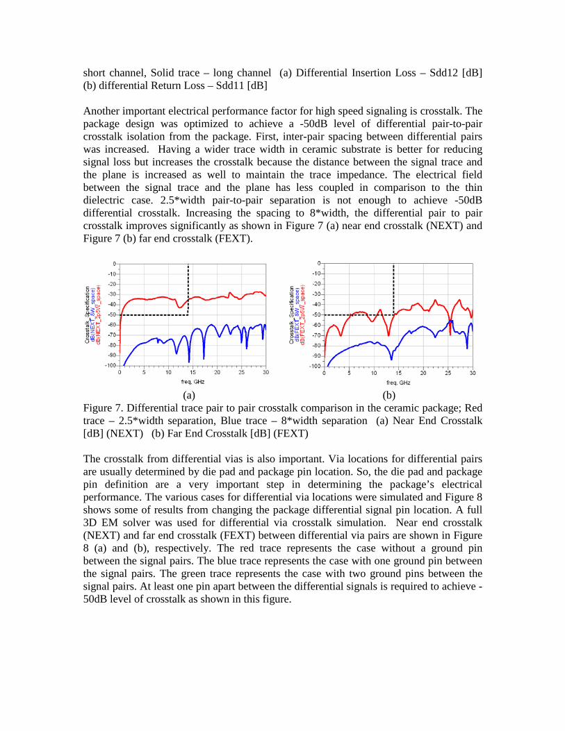
short channel, Solid trace – long channel (a) Differential Insertion Loss – Sdd12 [dB] (b) differential Return Loss – Sdd11 [dB] Another important electrical performance factor for high speed signaling is crosstalk. The package design was optimized to achieve a -50dB level of differential pair-to-pair crosstalk isolation from the package. First, inter-pair spacing between differential pairs was increased. Having a wider trace width in ceramic substrate is better for reducing signal loss but increases the crosstalk because the distance between the signal trace and the plane is increased as well to maintain the trace impedance. The electrical field between the signal trace and the plane has less coupled in comparison to the thin dielectric case. 2.5*width pair-to-pair separation is not enough to achieve -50dB differential crosstalk. Increasing the spacing to 8*width, the differential pair to pair crosstalk improves significantly as shown in Figure 7 (a) near end crosstalk (NEXT) and Figure 7 (b) far end crosstalk (FEXT).
(a) (b) Figure 7. Differential trace pair to pair crosstalk comparison in the ceramic package; Red trace – 2.5*width separation, Blue trace – 8*width separation (a) Near End Crosstalk [dB] (NEXT) (b) Far End Crosstalk [dB] (FEXT) The crosstalk from differential vias is also important. Via locations for differential pairs are usually determined by die pad and package pin location. So, the die pad and package pin definition are a very important step in determining the package’s electrical performance. The various cases for differential via locations were simulated and Figure 8 shows some of results from changing the package differential signal pin location. A full 3D EM solver was used for differential via crosstalk simulation. Near end crosstalk (NEXT) and far end crosstalk (FEXT) between differential via pairs are shown in Figure 8 (a) and (b), respectively. The red trace represents the case without a ground pin between the signal pairs. The blue trace represents the case with one ground pin between the signal pairs. The green trace represents the case with two ground pins between the signal pairs. At least one pin apart between the differential signals is required to achieve -50dB level of crosstalk as shown in this figure.
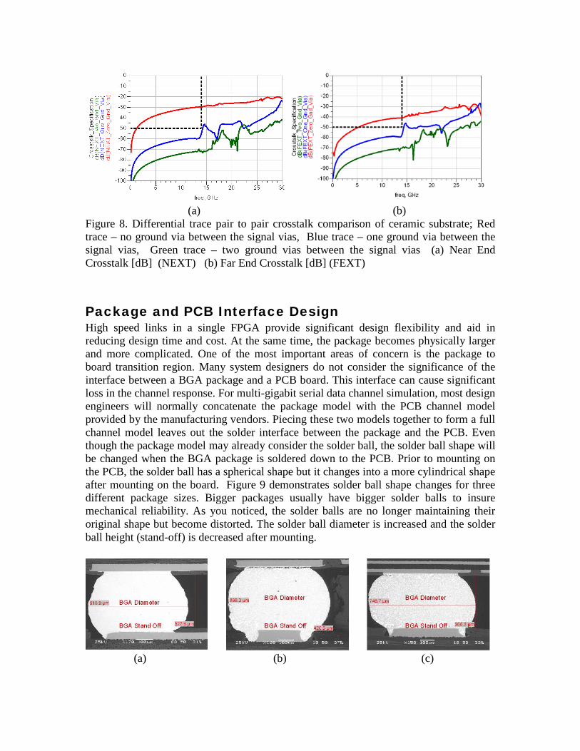
(a) (b) Figure 8. Differential trace pair to pair crosstalk comparison of ceramic substrate; Red trace – no ground via between the signal vias, Blue trace – one ground via between the signal vias, Green trace – two ground vias between the signal vias (a) Near End Crosstalk [dB] (NEXT) (b) Far End Crosstalk [dB] (FEXT)
Package and PCB Interface Design High speed links in a single FPGA provide significant design flexibility and aid in reducing design time and cost. At the same time, the package becomes physically larger and more complicated. One of the most important areas of concern is the package to board transition region. Many system designers do not consider the significance of the interface between a BGA package and a PCB board. This interface can cause significant loss in the channel response. For multi-gigabit serial data channel simulation, most design engineers will normally concatenate the package model with the PCB channel model provided by the manufacturing vendors. Piecing these two models together to form a full channel model leaves out the solder interface between the package and the PCB. Even though the package model may already consider the solder ball, the solder ball shape will be changed when the BGA package is soldered down to the PCB. Prior to mounting on the PCB, the solder ball has a spherical shape but it changes into a more cylindrical shape after mounting on the board. Figure 9 demonstrates solder ball shape changes for three different package sizes. Bigger packages usually have bigger solder balls to insure mechanical reliability. As you noticed, the solder balls are no longer maintaining their original shape but become distorted. The solder ball diameter is increased and the solder ball height (stand-off) is decreased after mounting.
(a) (b) (c)

(a) 17 x 17 mm (b) 35 x 35 mm (c) 42.5 x 42.5mm
Stand Off Diameter Stand Off Diameter Stand Off Diameter
327.6um 615.9um 420.6um 666.3um 365.3um 748.7um
Figure 9. Solder Balls between Substrate and PCB after Mounting (a) 17mm x 17mm BGA (b) 35mm x 35mm BGA (c) 42.5mm x 42.5mm BGA This phenomenon causes additional parasitics in a channel. Notice in Figure 9, the solder ball becomes larger than the BGA solder pad on the PCB after mounting. The distorted solder ball with pad and the nearby ground plane layer on both the package substrate and the PCB create additional capacitance which degrades overall system performance by adding more reflections and jitter due to the impedance discontinuity. Figure 10 shows a TDR simulation that investigates changing the solder ball size and shape in the interface area. X-axis is time and y-axis is the reflective waveform voltage. In this TDR graph, a deeper valley represents a more capacitive characteristic and a shallower valley represents a less capacitive characteristic. As you can see, the capacitance is varying significantly due to changes in solder ball shapes. In this particular case, 0.16mm bigger diameter solder ball results in approximately a 15ohm differential impedance drop in the interface area.
Figure 10. TDR Simulation with Various Solder Ball Size Impedance changes due to board mounting were also verified by full-wave 3D EM field simulation. A similar study has been performed previously [8]. The BGA package and the PCB board were individually simulated using a full-wave 3D EM field solver. Each s-parameter model from simulation was concatenated into a circuit simulator, HSPICE or ADS, to generate a set of cascaded s-parameters. Afterwards, the BGA package was attached to the PCB board in the full-wave 3D EM field solver and a composite model was generated. The full-wave 3D EM field extraction was performed on the composite

BGA/PCB structure to generate s-parameters. The s-parameters from the different methods were compared to investigate the differences.
(a) (b)
Figure 11. Concatenated Model vs. End-to-End Combined Model: Solid Red Line – Combined Model, Dash Blue Line – Concatenated Model, Dot Pink Line – Concatenated Model with Solder Ball Shape Change (a) Differential Return Loss [Sdd11] (b) Differential Insertion Loss [Sdd21] The s-parameters in Figure 11 show a clear difference between the models. The left graph of s-parameters is a differential return loss graph and the right graph of s-parameters is a differential insertion loss graph. The solid red line represents a package substrate and a board combined into one model in a simulator and the blue dashed line represents a concatenated model, which is a package substrate and board simulated separately and then cascaded in the circuit simulator, without considering of the solder ball shape changes. As you can see in the figure, the concatenated model has a much better performance because the model does not include additional capacitance caused by solder ball shape changes. Then, next consideration is the solder ball shape changes in the concatenated model. The dotted pink line in the figure shows this. The results correlate more closely to the combined model now, although not perfectly matched. This is due to the additional capacitance between the solder ball (bigger than PCB solder pad) and the PCB ground plane (underneath PCB solder pad) which was not considered in the concatenated model even though the solder ball shape changes were taken into account. The simulation would need to consider all of these effects to achieve better accuracy. Multiple techniques can be used to compensate for the capacitance from solder ball transition. Cutting the ground plane in the area around the interface as shown in Figure 12 is commonly used compensation technique utilized in the industry today. Since capacitive parasitics are so significant for a large package, cutting multiple ground plane layers for both package substrate and PCB may be required. Other compensation structures like the spiral via structure in the package can also be used but the wave length is too short for even this high frequency, so we need to be careful in using it due to the cut-off frequency limitation. [9]

Solder Ball
PKG PAD
PCB PAD
PCB GND
PKG GND
Solder Ball
GND CUT
GND CUT
Figure 12. Cutting Ground Planes on Both Package Substrate and PCB
System Simulation using SSI, LTCC Package and PCB model After the silicon interposer, package, PCB and the interface design were optimized, full system simulations were performed. Higher silicon substrate resistivity of 20 ~ 30 ohm-cm is chosen to be used for the passive interposer. On the other hand, the technology of manufacturing packages and PCBs are evolving simultaneously such as LTCC (Low Temperature Co-Fired Ceramic) package and low loss PCB material. In addition, the capability of transceiver is another degree of freedom of channel design. Therefore, it is worthwhile to investigate if the equalization functions available in SerDes transceiver can be exerted to compensate the degraded eye and BER bathtub. In the channel simulation, models of the 11.4mm LTCC package and a 6 inch Megtron6 signal trace were generated. Then, two interposers with silicon substrate resistivity of 20 and 30ohm-cm were added to investigate the impacts on SerDes signal transmission. To visualize their impacts on the package plus board channel in the frequency domain, the differential transmitted s-parameters versus frequency are overlaid on the same plot as shown in Figure 13.
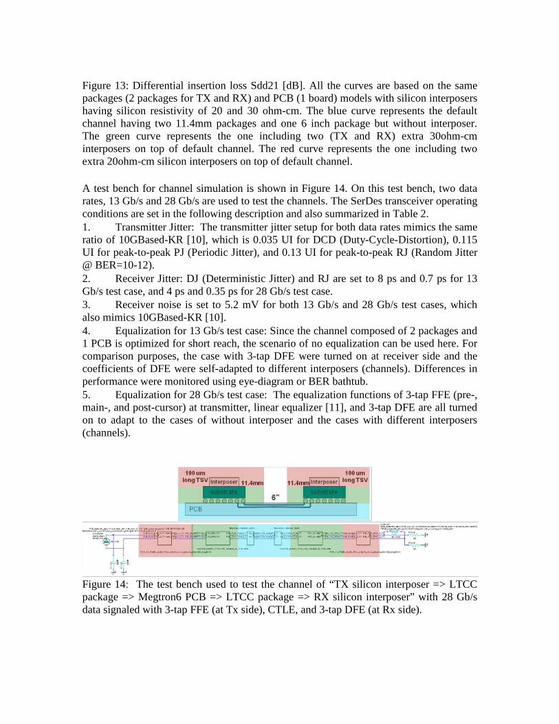
Figure 13: Differential insertion loss Sdd21 [dB]. All the curves are based on the same packages (2 packages for TX and RX) and PCB (1 board) models with silicon interposers having silicon resistivity of 20 and 30 ohm-cm. The blue curve represents the default channel having two 11.4mm packages and one 6 inch package but without interposer. The green curve represents the one including two (TX and RX) extra 30ohm-cm interposers on top of default channel. The red curve represents the one including two extra 20ohm-cm silicon interposers on top of default channel. A test bench for channel simulation is shown in Figure 14. On this test bench, two data rates, 13 Gb/s and 28 Gb/s are used to test the channels. The SerDes transceiver operating conditions are set in the following description and also summarized in Table 2. 1. Transmitter Jitter: The transmitter jitter setup for both data rates mimics the same ratio of 10GBased-KR [10], which is 0.035 UI for DCD (Duty-Cycle-Distortion), 0.115 UI for peak-to-peak PJ (Periodic Jitter), and 0.13 UI for peak-to-peak RJ (Random Jitter @ BER=10-12). 2. Receiver Jitter: DJ (Deterministic Jitter) and RJ are set to 8 ps and 0.7 ps for 13 Gb/s test case, and 4 ps and 0.35 ps for 28 Gb/s test case. 3. Receiver noise is set to 5.2 mV for both 13 Gb/s and 28 Gb/s test cases, which also mimics 10GBased-KR [10]. 4. Equalization for 13 Gb/s test case: Since the channel composed of 2 packages and 1 PCB is optimized for short reach, the scenario of no equalization can be used here. For comparison purposes, the case with 3-tap DFE were turned on at receiver side and the coefficients of DFE were self-adapted to different interposers (channels). Differences in performance were monitored using eye-diagram or BER bathtub. 5. Equalization for 28 Gb/s test case: The equalization functions of 3-tap FFE (pre-, main-, and post-cursor) at transmitter, linear equalizer [11], and 3-tap DFE are all turned on to adapt to the cases of without interposer and the cases with different interposers (channels).
Figure 14: The test bench used to test the channel of “TX silicon interposer => LTCC package => Megtron6 PCB => LTCC package => RX silicon interposer” with 28 Gb/s data signaled with 3-tap FFE (at Tx side), CTLE, and 3-tap DFE (at Rx side).
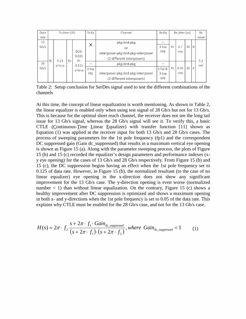
Table 2: Setup conclusion for SerDes signal used to test the different combinations of the channels At this time, the concept of linear equalization is worth mentioning. As shown in Table 2, the linear equalizer is enabled only when using test signal of 28 Gb/s but not for 13 Gb/s. This is because for the optimal short reach channel, the receiver does not see the long tail issue for 13 Gb/s signal, whereas the 28 Gb/s signal will see it. To verify this, a basic CTLE (Continuous-Time Linear Equalizer) with transfer function [11] shown as Equation (1) was applied at the receiver input for both 13 Gb/s and 28 Gb/s cases. The process of sweeping parameters for the 1st pole frequency (fp1) and the correspondent DC suppressed gain (Gain dc_suppressed) that results in a maximum vertical eye opening is shown as Figure 15 (a). Along with the parameter sweeping process, the plots of Figure 15 (b) and 15 (c) recorded the equalizer’s design parameters and performance indexes (x-y eye opening) for the cases of 13 Gb/s and 28 Gb/s respectively. From Figure 15 (b) and 15 (c), the DC suppression begins having an effect when the 1st pole frequency set to 0.125 of data rate. However, in Figure 15 (b), the normalized resultant (to the case of no linear equalizer) eye opening in the x-direction does not show any significant improvement for the 13 Gb/s case. The y-direction opening is even worse (normalized number < 1) than without linear equalization. On the contrary, Figure 15 (c) shows a healthy improvement after DC suppression is optimized and shows a maximum opening in both x- and y-directions when the 1st pole frequency is set to 0.05 of the data rate. This explains why CTLE must be enabled for the 28 Gb/s case, and not for the 13 Gb/s case.
( ) ( ) 1 ,22
22)( seddc_suppres
21
seddc_suppres12 <
⋅+⋅⋅+⋅⋅+
⋅= Gainwherefsfs
GainfsfsH
πππ
π (1)

(a)
(b)
(c) Figure 15: (a) The way of figuring out the optimal setting for linear equalizer. (b) & (c) The optimal DC suppression gain, correspondent x-and y-opening of the eye diagram when lowering down the 1st pole frequency of the linear equalizer. The testing results are overlaid in the bathtub plots of Figure 16. In Figure 16(a), the red curves show the bathtub BER plot without turning on any equalization and the result shows the interposer can bring down the eye opening@ BER=1e-14 from 0.5543UI (without interposer) to 0.5441UI (for 30 ohm-cm interposer) and 0.5082UI (for 20 ohm-cm interposer). The blue curves show the bathtub BER plot with 3-tap DFE turning on at receiver side and result shows the 20 ohm-cm interposer can bring down the eye opening@ BER=1e-14 from 0.67UI (for without interposer and 30 ohm-cm interposer) to
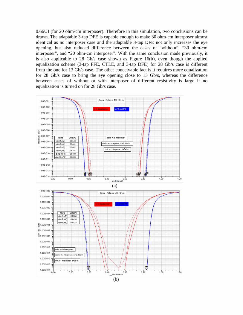
0.66UI (for 20 ohm-cm interposer). Therefore in this simulation, two conclusions can be drawn. The adaptable 3-tap DFE is capable enough to make 30 ohm-cm interposer almost identical as no interposer case and the adaptable 3-tap DFE not only increases the eye opening, but also reduced difference between the cases of “without”, “30 ohm-cm interposer”, and “20 ohm-cm interposer”. With the same conclusion made previously, it is also applicable to 28 Gb/s case shown as Figure 16(b), even though the applied equalization scheme (3-tap FFE, CTLE, and 3-tap DFE) for 28 Gb/s case is different from the one for 13 Gb/s case. The other conceivable fact is it requires more equalization for 28 Gb/s case to bring the eye opening close to 13 Gb/s, whereas the difference between cases of without or with interposer of different resistivity is large if no equalization is turned on for 28 Gb/s case.
(a)
(b)
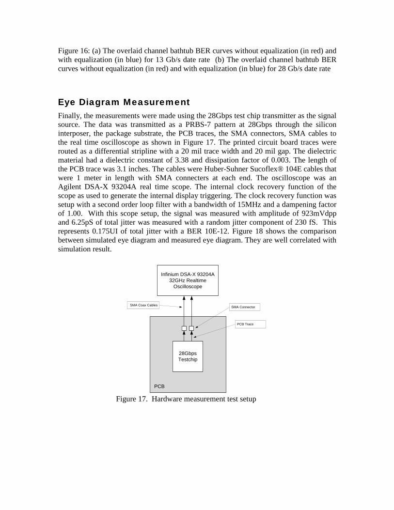
Figure 16: (a) The overlaid channel bathtub BER curves without equalization (in red) and with equalization (in blue) for 13 Gb/s date rate (b) The overlaid channel bathtub BER curves without equalization (in red) and with equalization (in blue) for 28 Gb/s date rate
Eye Diagram Measurement Finally, the measurements were made using the 28Gbps test chip transmitter as the signal source. The data was transmitted as a PRBS-7 pattern at 28Gbps through the silicon interposer, the package substrate, the PCB traces, the SMA connectors, SMA cables to the real time oscilloscope as shown in Figure 17. The printed circuit board traces were routed as a differential stripline with a 20 mil trace width and 20 mil gap. The dielectric material had a dielectric constant of 3.38 and dissipation factor of 0.003. The length of the PCB trace was 3.1 inches. The cables were Huber-Suhner Sucoflex® 104E cables that were 1 meter in length with SMA connecters at each end. The oscilloscope was an Agilent DSA-X 93204A real time scope. The internal clock recovery function of the scope as used to generate the internal display triggering. The clock recovery function was setup with a second order loop filter with a bandwidth of 15MHz and a dampening factor of 1.00. With this scope setup, the signal was measured with amplitude of 923mVdpp and 6.25pS of total jitter was measured with a random jitter component of 230 fS. This represents 0.175UI of total jitter with a BER 10E-12. Figure 18 shows the comparison between simulated eye diagram and measured eye diagram. They are well correlated with simulation result.
Infinium DSA-X 93204A 32GHz Realtime
Oscilloscope
28Gbps Testchip
PCB
SMA Connector
PCB Trace
SMA Coax Cables
Figure 17. Hardware measurement test setup
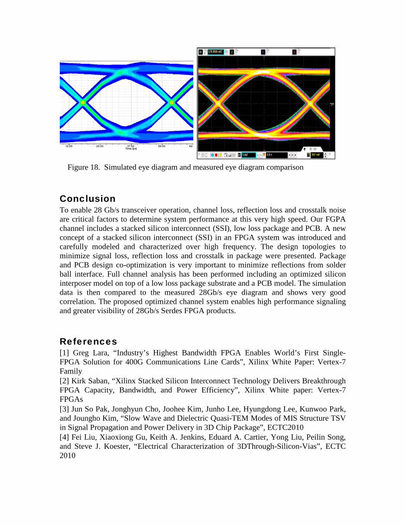
Figure 18. Simulated eye diagram and measured eye diagram comparison
Conclusion To enable 28 Gb/s transceiver operation, channel loss, reflection loss and crosstalk noise are critical factors to determine system performance at this very high speed. Our FGPA channel includes a stacked silicon interconnect (SSI), low loss package and PCB. A new concept of a stacked silicon interconnect (SSI) in an FPGA system was introduced and carefully modeled and characterized over high frequency. The design topologies to minimize signal loss, reflection loss and crosstalk in package were presented. Package and PCB design co-optimization is very important to minimize reflections from solder ball interface. Full channel analysis has been performed including an optimized silicon interposer model on top of a low loss package substrate and a PCB model. The simulation data is then compared to the measured 28Gb/s eye diagram and shows very good correlation. The proposed optimized channel system enables high performance signaling and greater visibility of 28Gb/s Serdes FPGA products.
References [1] Greg Lara, “Industry’s Highest Bandwidth FPGA Enables World’s First Single-FPGA Solution for 400G Communications Line Cards”, Xilinx White Paper: Vertex-7 Family [2] Kirk Saban, “Xilinx Stacked Silicon Interconnect Technology Delivers Breakthrough FPGA Capacity, Bandwidth, and Power Efficiency”, Xilinx White paper: Vertex-7 FPGAs [3] Jun So Pak, Jonghyun Cho, Joohee Kim, Junho Lee, Hyungdong Lee, Kunwoo Park, and Joungho Kim, “Slow Wave and Dielectric Quasi-TEM Modes of MIS Structure TSV in Signal Propagation and Power Delivery in 3D Chip Package”, ECTC2010 [4] Fei Liu, Xiaoxiong Gu, Keith A. Jenkins, Eduard A. Cartier, Yong Liu, Peilin Song, and Steve J. Koester, “Electrical Characterization of 3DThrough-Silicon-Vias”, ECTC 2010

[5] Joohee Kim, Jun So Pak, Jonghyun Cho, Junho Lee, Hyungdong Lee, Kunwoo Park and Joungho Kim , “Modeling and Analysis of Differential Signal Through Silicon Via (TSV) in 3D IC”, CPMT Symposium Japan 2010. [6] Agilent Application Note, “Ultra-low Impedance Measurements Using 2-port Measurement” [7] Namhoon Kim, Zhaoyin Daniel We, Arif Rahman, Dongwook Kim, and Paul Wu, “Through Silicon Via (TSV) Design Considering Technology Challenges for Very High-Speed Signal Transmission”, DesignCon 2011, Santa Clara, Jan. 31 - Feb. 3, 2011 [8] Martin Schauer, Hong Ahn, Namhoon Kim, Chris Wyland, and Paul Wu, “Efficient Modeling and Simulation for Package-PCB Co-Design and Co-Optimization”, DesignCon 2010 [9] Namhoon Kim, Hongsik Ahn, Chris Wyland, Ray Anderson, and Paul Wu, “Spiral Via Structure in a BGA Package to Mitigate Discontinuities in Multi-Gigabit SERDES System”, ECTC2010 [10] “IEEE Std 802.3ap™-2007 (Amendment to IEEE Std 802.3™-2005)”, pp. 92 and 100, IEEE Computer Society. [11] “Nexxim Simulator of Designer Online Help”, Chapter 5 VerifEye and QuickEye Anslyses, pp. 5-82, ANSYS, Inc..