design summary for microsip-enabled tps8267xsip - ti · pdf file 1q 2011 design summary for...
TRANSCRIPT

1Q 2011www.ti.com
Design Summary forMicroSiP™-enabled TPS8267xSiP
Introduction
Package Label
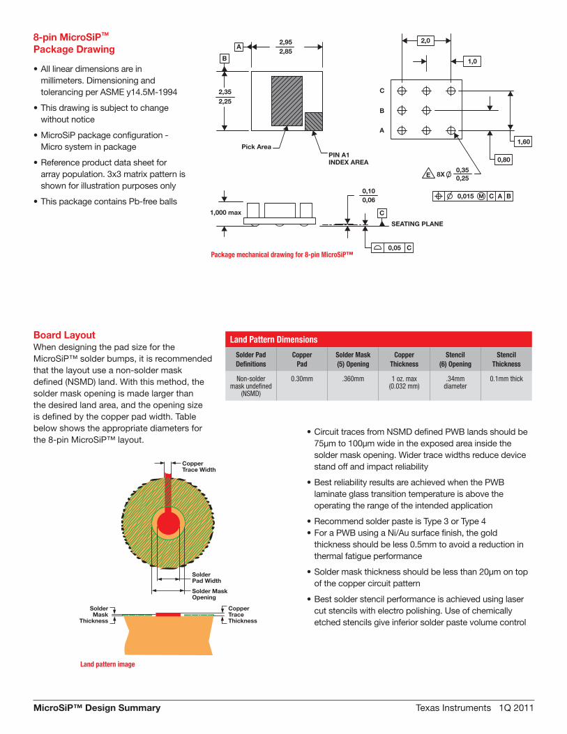
8-pin Package Drawing
Board Layout
Packaging Information
MicroSiP Surface Mount
Board-Level Reliability Data
Electrical Characterization
Thermal Evaluation
Rework
FAQ
**Bumppitchis1,0mminxdirection,0,8mminydirection.
IntroductionAsthemarketplacecontinuestodemandsizereductionsinportableelectronicproducts,theneedforsmallerpackagingandsmallersubsystempackagingbecomesparamount.Inaddition,sizereductionscannolongerfocusonlyonpackagesurfacearea,meaninglengthandwidth,butalsomustdecreasethepackagethicknessandweight.Toaddresstheserapidlyevolvingcustomerrequirements,TIhasintroducedMicroSiP™,thelatestinnovationinSystem-in-Package(SiP)technologyintegratingICandpassivecomponentsinasingledevicefeaturinganembeddedPicoStar™.ThesmallMicroSiPfootprintprovidesastand-alonepowersupplyplatformdrivinganunprecedentedpowertopackagedensityof90mA/mm2.MicroSiP(packagedesignatorSIP)isofferedtodayina8-pinformatfortheTPS8267x.
Packaging Attributes
Attribute 8-ball
Ball Pitch 0,8/1,0mm**
Ball Diameter 0,30mm
Package Length ~2,30mm
Package Width ~2,90mm
Package Height 1,0mm max
Bump Matrix 3x3
Bump Metallurgy SAC305
Moisture Level Level 2 at 260°C
MicroSiP™ package
2,90mm1,0mm Max.
2,30
mm
MicroSiP™ cross-sectional view
PicoStar™
FR-4 Laminate Substrate
Inductor
BGASolder Bumps
8-pin MicroSiP™
Package Drawing
MicroSiP™ Design Summary TexasInstruments1Q2011
PIN A1INDEX AREA
Pick Area
2,35
2,95A
B2,85
2,25
2,0
0,015
0,35
0,80
1,60
0,25
M C A
E 8X
B
C
B
A
1,0
SEATING PLANE
1,000 max
0,10
0,05 C
0,06
C
PIN A1INDEX AREA
Pick Area
2,35
2,95A
B2,85
2,25
2,0
0,015
0,35
0,80
1,60
0,25
M C A
E 8X
B
C
B
A
1,0
SEATING PLANE
1,000 max
0,10
0,05 C
0,06
C
PIN A1INDEX AREA
Pick Area
2,35
2,95A
B2,85
2,25
2,0
0,015
0,35
0,80
1,60
0,25
M C A
E 8X
B
C
B
A
1,0
SEATING PLANE
1,000 max
0,10
0,05 C
0,06
C
•Alllineardimensionsareinmillimeters.DimensioningandtolerancingperASMEy14.5M-1994
•Thisdrawingissubjecttochangewithoutnotice
•MicroSiPpackageconfiguration-Microsysteminpackage
•Referenceproductdatasheetforarraypopulation.3x3matrixpatternisshownforillustrationpurposesonly
•ThispackagecontainsPb-freeballs
•CircuittracesfromNSMDdefinedPWBlandsshouldbe75µmto100µmwideintheexposedareainsidethesoldermaskopening.Widertracewidthsreducedevicestandoffandimpactreliability
•BestreliabilityresultsareachievedwhenthePWBlaminateglasstransitiontemperatureisabovetheoperatingtherangeoftheintendedapplication
•RecommendsolderpasteisType3orType4•ForaPWBusingaNi/Ausurfacefinish,thegold
thicknessshouldbeless0.5mmtoavoidareductioninthermalfatigueperformance
•Soldermaskthicknessshouldbelessthan20µmontopofthecoppercircuitpattern
•Bestsolderstencilperformanceisachievedusinglasercutstencilswithelectropolishing.Useofchemicallyetchedstencilsgiveinferiorsolderpastevolumecontrol
Board LayoutWhendesigningthepadsizefortheMicroSiP™solderbumps,itisrecommendedthatthelayoutuseanon-soldermaskdefined(NSMD)land.Withthismethod,thesoldermaskopeningismadelargerthanthedesiredlandarea,andtheopeningsizeisdefinedbythecopperpadwidth.Tablebelowshowstheappropriatediametersforthe8-pinMicroSiP™layout.
Land Pattern Dimensions
Solder PadDefinitions
CopperPad
Solder Mask(5) Opening
CopperThickness
Stencil(6) Opening
StencilThickness
Non-solder mask undefined
(NSMD)
0.30mm .360mm 1 oz. max(0.032 mm)
.34mm diameter
0.1mm thick
CopperTraceThickness
SolderMask
Thickness
SolderPad Width
CopperTrace Width
Solder MaskOpening
Land pattern image
Package mechanical drawing for 8-pin MicroSiP™

MicroSiP™ Design Summary TexasInstruments1Q2011
Packaging Information
Nounderfilloradhesivewaseitherusedorrequiredforthesepackages.Preconditioning:3passreflow+24hr/125°Cbake0.7mmthickFR4epoxymainboard.
8-pin MicroSiP™
Test Parameters Results (tfirst fail)
Drop 1500G/1.0ms pulse > 100 drops
Temp Cycle -40/125°C, 2 cycles/hr > 1000 cycles
MicroSiP™ Surface MountSurfacemountingofMicroSiPpackagesisbroadlysimilartoBGApackageassembly.TIrecommendstheuseofPb-freesolderpasteappliedviaa0.1mmthickstencil(criticalstencildimensionsshowninboardlayoutsubsection).Thepasteacts:toaidwettingoftheSiPbumptotheboardland,toholdtheSiPinplaceduringreflow,andtocontributemetalvolumeoftheresultantsolderjoint.StandardJEDECreflowprofilesfornear-eutecticSnAgCusolderalloysaresuggested(max260°C).Board-SiPsolderjointheightis120µm.
SiP Cu Trace
Main Board Cu Land
SiP-Main BoardSolder Joint
Inductor
SiP Substrate
Main Board
P2T
T2
T1
E2
D1
E1
F
W
Bo
Ao
Po
Ko
[10 pitches cumulativetolerance on tape +0.2 mm]
Embossment for cavity size,see note 1 Table 2
User Direction of Unreeling
Center Lines of Cavity
Cover Tape
B1 is for tape feeder reference only,including draft concentric about Bo
Do
B1
S1
Pin 1
Package Carrier-Tape Width (W) Pocket Pitch (P) Pocket Width (Ao) Pocket Length (Bo) Pocket Depth (Ko) Reel Diameter
MicroSip™ 8.0 ± 0.30 4.0 ± 0.10 2.45 ± 0.05 3.05 ± 0.05 1.1 ± 0.05 178
Do D1 Min E1 Po P2 R Ref. S1 Min. T Max. T1o Max.
1.5+0.1 -0.0 1.5 1.75 ± 0.1 4.0 ± 0. 2.0 ± .05 30 0.6 0.6 0.25
Orient component as shown with Pin 1 closest to the tape sprocket holes on tape leading edge. All dimensions in millimeters.
Tape and reel
Cross-section of MicroSiP™ mounted to main board
Board-Level Reliability Data

MicroSiP™ Design Summary TexasInstruments1Q2011
Thermal Image of MicroSiP™ when IC is dissipating 0.45W. Ambient temperature is 22°C, max junction temperature is 72°C. For thermal modeling, a value of QJA=125°C/W provides an excellent initial estimate of thermal performance.
Close-up of MicroSiP™ mounted to the TI EVM
Thermal Evaluation
100
90
80
70
60
50
40
30
20
10
00.1 1 10 100 1000
I - Load Current - mAO
% - y
cn
eiciff
E
V = 1.8 VO
V = 2.7 VPFM/PWM Operation
I
V = 3.6 VPFM/PWM Operation
I
V = 4.2 VPFM/PWM Operation
I V = 3.6 VForced PWM Operation
I
100
90
80
70
60
50
40
30
20
10
00.1 1 10 100 1000
I - Load Current - mAO
% - y
cn
eiciff
E
V = 1.2 VO V = 2.7 VPFM/PWM Operation
I
V = 3.6 VPFM/PWM Operation
I
V = 4.2 VPFM/PWM Operation
I
V = 3.6 VForced PWM Operation
I
100
90
80
70
60
50
40
30
20
10
00.1 1 10 100 1000
I - Load Current - mAO
% - y
cn
eiciff
E
V = 1.8 VO
V = 2.7 VPFM/PWM Operation
I
V = 3.6 VPFM/PWM Operation
I
V = 4.2 VPFM/PWM Operation
I V = 3.6 VForced PWM Operation
I
100
90
80
70
60
50
40
30
20
10
00.1 1 10 100 1000
I - Load Current - mAO% -
yc
nei
ciffE
V = 1.2 VO V = 2.7 VPFM/PWM Operation
I
V = 3.6 VPFM/PWM Operation
I
V = 4.2 VPFM/PWM Operation
I
V = 3.6 VForced PWM Operation
I
SIP-8(TOP VIEW) (BOTTOM VIEW)
SIP-8
A1
B1
C1
A2
B2
C2GND
MODE
VOUT
GND
A3
C3
VIN
EN
A3
C3
A2
B2
C2GND
EN
VIN
GNDC1
VOUT
MODE
A1
B1
PIN ASSIGNMENTS
Pin Description
Plot of efficiency as a function of current forA) Vo=1.8V and B) Vo=1.2V
Electrical Characterization
A - Efficiency vs Load Current
B - Efficiency vs Load Current

MicroSiP™ Design Summary TexasInstruments1Q2011
Package LabelTypicalviewoftheSiPmarkinginthetopofthepackage.Markingincludesbothlottracecodingandpin1indicator.
Code:CC-DeviceCodeYML-DateCodeLSB-Lot/Site/BoardTraceCode
FAQQ: What is a MicroSiP™?A: MicroSiP™isaminiaturizedSystem-in-Package(SiP)thatintegratesSiliconintegratedcircuits(IC’s)withpassive
componentsinaBGA-format.Typically,thepassivesarearrangedonthetop,BGAballsarearrayedonthebottomandtheintegratedcircuitPicoStar™packageisembeddedinthelaminatesubstrate.TheMicroSiPcanbeeithersquareorrectangular.
Q: How is a MicroSiP™ different from a wafer-chip-scale-package (WCSP)?A: TheMicroSiPpackageincludesICandpassiveswhiletheWCSPisonlyanIC.Forexample,theTPS8267xpackagedin
MicroSiPintegratesaDC-DCconverterwithinductorandinput-outputcapstoprovideastand-alonepowersupply.
Q: What is a PicoStar™?A: PicoStar™isadie-sizedpackagedesignedtobeembeddedinHDIlaminatesubstrates.
Q: Is this a lead-free (Pb-free) package?A: Yes,MicroSiPpackagescomplywithlead-freeenvironmentalpolicies.TheBGAbumpsandthepassivejointsbothare
SAC305(3%Ag,0.5%Cu,balanceSn).
Q: What land pad size should I design on my board for these packages?A: TIrecommendsthattheboardlandcloselymatchthelandsizeontheSiP—300umdiameter,non-soldermaskdefined.
MicroSiPmountedtoa0.7mmthickPCBwithOSPpadseasilywithstands1000cyclesfrom-40to125°C(15minutedwells).
Q: Are there any special MicroSiP™ placement requirements?A: MovementoftheMicroSiPfromT&RtoplacementonthePCBcanbetreatedasasimilarsizedBGA.TheMicroSiPshould
bepickedfromtheinductortopsurfaceemployinga~1mmdiameternozzle/rubbertip(contactareabetween0.5-1.0mm2).
Q: Can I mount MicroSiP™ to the bottom of the PCB board?A: Yesyoucan.Ideally,thefirstandsecondreflowprofilesareidentical.ThereflowprofileshouldfollowJEDECstandardsfor
SMTofnear-eutecticSnAgCusolder.
Q: Can the MicroSiP™ withstand multiple reflows?A: Yes.Boardlevelreliabilitytestingwasperformedafter3passreflow(1passforassembly,then2additionalpasses).
Ingeneral,assemblyoftheMicroSiPpackagecanbetreatedexactlylikeaBGA.
Q: What alignment accuracy is possible?A: TIrecommendsprintingalead-freesolderpasteasdescribedintheboardlayoutsubsectionbeforeplacementofthe
MicroSiP.AlignmentaccuracydependsonboardpadtoleranceandMicroSiPplacementaccuracy.MicroSiPpackagesself-alignduringreflow—finalalignmentaccuracyisverylikelybetterthanplacementaccuracy.
Q: How do board assembly yields of MicroSiP™ compare to a similar BGA?A: ForaBGAofsimilarsizeandpitch,theassemblyyieldisidenticaltotheMicroSiPpackage.
MicroSiP labeling is shown in the top view image. Marking includes both lot trace coding and pin 1 indicator
ReworkItisstronglyrecommendedthatthePCBwithmountedSMTdevicesbebakedpriortoanyreworksothatabsorbedmoistureisremoved(SeeJ-STD-033formoredetails).ThereworkprocessshouldbecharacterizedsuchthatthetemperatureoftheMicroSiP™packageandsurroundingPCBareaarecontrolled.Eitheranattachedthermocoupleoraninfraredcameraworkswelltodeterminearepeatableheatingprofile.
Componentremovalprocessexample:• Alignnozzleoverparttoberemoved• Maintainnozzle1.27mmoverthepackage• Preheatboardto90°C,nozzlewarmingat20%airflow/125°C• Soakstageat20%airflow/225°C/90seconds• Rampstageat25%airflow/335°C/30seconds• Reflowstageat25%airflow/370°C/65seconds• Enablevacuum,lowernozzle,removeinductorfromMicroSiP• DiscardInductor• Repositionnozzle,reheatat25%airflow/370°C/20seconds• Enablevacuum,lowernozzle,removeMicroSiPfromPCB• Cooldownstageat40%airflow/25°C/50seconds• TurnoffvacuumandremovepartMicroSiPfromnozzle• Avoidhandlingdamageoftheremovedunit• Donotreuse/repairtheremovedunit
Componentreplacementprocessexample:• Applysolderpastetoboardusingamicro-stencil• AlignMicroSiPoverboardlandpads• PlaceMicroSiPonboard.Careshouldbetaken
topreventovertravelduringplacementwhichmaydamagethepackageorvacuumtip
• Raisenozzle1.27mm• Preheatboardto90°C,nozzlewarmingat20%air
flow/125°C• Soakstageat20%airflow/225°C/90seconds• Rampstageat25%airflow/335°C/30seconds• Reflowstageat25%airflow/370°C/65seconds• Cooldownstageat40%airflow/25°C/50seconds
Air-VacEngineering:Air-VacEngineering(www.air-vac-eng.com)hasestablishedheatingprofilesandtoolingrecommendationsfortheirHotGas(convection)reworkequipment,DRS-24NC.
NozzleNMX188DVG-0.18”Exhaustopening-VTMX020-35VacuumTip
Comparable hot gas (convection heating) rework equipment from
other vendors can also be used successfully.
TI Worldwide Technical SupportInternetTI Semiconductor Product Information Center Home Pagesupport.ti.comTI E2E™ Community Home Pagee2e.ti.com
Product Information CentersAmericas Phone +1(972)644-5580
Brazil Phone 0800-891-2616
Mexico Phone 0800-670-7544
Fax +1(972)927-6377 Internet/Email support.ti.com/sc/pic/americas.htm
Europe, Middle East, and AfricaPhone
EuropeanFreeCall 00800-ASK-TEXAS (0080027583927)
International +49(0)8161802121
RussianSupport +7(4)959810701
Note:TheEuropeanFreeCall(TollFree)numberisnotactiveinallcountries.Ifyouhavetechnicaldifficultycallingthefreecallnumber,pleaseusetheinternationalnumberabove.
Fax +(49)(0)8161802045Internet support.ti.com/sc/pic/euro.htmDirectEmail [email protected]
JapanPhone Domestic 0120-92-3326Fax International +81-3-3344-5317 Domestic 0120-81-0036Internet/Email International support.ti.com/sc/pic/japan.htm Domestic www.tij.co.jp/pic
AsiaPhone International +91-80-41381665 Domestic Toll-FreeNumber Note:Toll-freenumbersdonotsupport
mobileandIPphones. Australia 1-800-999-084 China 800-820-8682 HongKong 800-96-5941 India 1-800-425-7888 Indonesia 001-803-8861-1006 Korea 080-551-2804 Malaysia 1-800-80-3973 NewZealand 0800-446-934 Philippines 1-800-765-7404 Singapore 800-886-1028 Taiwan 0800-006800 Thailand 001-800-886-0010Fax +8621-23073686Email [email protected]@ti.comInternet support.ti.com/sc/pic/asia.htm
B122010
Important Notice:TheproductsandservicesofTexasInstrumentsIncorporatedanditssubsidiariesdescribedhereinaresoldsubjecttoTI’sstandardtermsandconditionsofsale.CustomersareadvisedtoobtainthemostcurrentandcompleteinformationaboutTIproductsandservicesbeforeplacingorders.TIassumesnoliabilityforapplicationsassistance,customer’sapplicationsorproductdesigns,softwareperformance,orinfringementofpatents.Thepublicationofinformationregardinganyothercompany’sproductsorservicesdoesnotconstituteTI’sapproval,warrantyorendorsementthereof.
©2011TexasInstrumentsIncorporated
TheplatformbarandE2EaretrademarksofTexasInstruments.Allothertrademarksarethepropertyoftheirrespectiveowners.
SLIB006

IMPORTANT NOTICE
Texas Instruments Incorporated and its subsidiaries (TI) reserve the right to make corrections, modifications, enhancements, improvements,and other changes to its products and services at any time and to discontinue any product or service without notice. Customers shouldobtain the latest relevant information before placing orders and should verify that such information is current and complete. All products aresold subject to TI’s terms and conditions of sale supplied at the time of order acknowledgment.
TI warrants performance of its hardware products to the specifications applicable at the time of sale in accordance with TI’s standardwarranty. Testing and other quality control techniques are used to the extent TI deems necessary to support this warranty. Except wheremandated by government requirements, testing of all parameters of each product is not necessarily performed.
TI assumes no liability for applications assistance or customer product design. Customers are responsible for their products andapplications using TI components. To minimize the risks associated with customer products and applications, customers should provideadequate design and operating safeguards.
TI does not warrant or represent that any license, either express or implied, is granted under any TI patent right, copyright, mask work right,or other TI intellectual property right relating to any combination, machine, or process in which TI products or services are used. Informationpublished by TI regarding third-party products or services does not constitute a license from TI to use such products or services or awarranty or endorsement thereof. Use of such information may require a license from a third party under the patents or other intellectualproperty of the third party, or a license from TI under the patents or other intellectual property of TI.
Reproduction of TI information in TI data books or data sheets is permissible only if reproduction is without alteration and is accompaniedby all associated warranties, conditions, limitations, and notices. Reproduction of this information with alteration is an unfair and deceptivebusiness practice. TI is not responsible or liable for such altered documentation. Information of third parties may be subject to additionalrestrictions.
Resale of TI products or services with statements different from or beyond the parameters stated by TI for that product or service voids allexpress and any implied warranties for the associated TI product or service and is an unfair and deceptive business practice. TI is notresponsible or liable for any such statements.
TI products are not authorized for use in safety-critical applications (such as life support) where a failure of the TI product would reasonablybe expected to cause severe personal injury or death, unless officers of the parties have executed an agreement specifically governingsuch use. Buyers represent that they have all necessary expertise in the safety and regulatory ramifications of their applications, andacknowledge and agree that they are solely responsible for all legal, regulatory and safety-related requirements concerning their productsand any use of TI products in such safety-critical applications, notwithstanding any applications-related information or support that may beprovided by TI. Further, Buyers must fully indemnify TI and its representatives against any damages arising out of the use of TI products insuch safety-critical applications.
TI products are neither designed nor intended for use in military/aerospace applications or environments unless the TI products arespecifically designated by TI as military-grade or "enhanced plastic." Only products designated by TI as military-grade meet militaryspecifications. Buyers acknowledge and agree that any such use of TI products which TI has not designated as military-grade is solely atthe Buyer's risk, and that they are solely responsible for compliance with all legal and regulatory requirements in connection with such use.
TI products are neither designed nor intended for use in automotive applications or environments unless the specific TI products aredesignated by TI as compliant with ISO/TS 16949 requirements. Buyers acknowledge and agree that, if they use any non-designatedproducts in automotive applications, TI will not be responsible for any failure to meet such requirements.
Following are URLs where you can obtain information on other Texas Instruments products and application solutions:
Products Applications
Audio www.ti.com/audio Communications and Telecom www.ti.com/communications
Amplifiers amplifier.ti.com Computers and Peripherals www.ti.com/computers
Data Converters dataconverter.ti.com Consumer Electronics www.ti.com/consumer-apps
DLP® Products www.dlp.com Energy and Lighting www.ti.com/energy
DSP dsp.ti.com Industrial www.ti.com/industrial
Clocks and Timers www.ti.com/clocks Medical www.ti.com/medical
Interface interface.ti.com Security www.ti.com/security
Logic logic.ti.com Space, Avionics and Defense www.ti.com/space-avionics-defense
Power Mgmt power.ti.com Transportation and www.ti.com/automotiveAutomotive
Microcontrollers microcontroller.ti.com Video and Imaging www.ti.com/video
RFID www.ti-rfid.com Wireless www.ti.com/wireless-apps
RF/IF and ZigBee® Solutions www.ti.com/lprf
TI E2E Community Home Page e2e.ti.com
Mailing Address: Texas Instruments, Post Office Box 655303, Dallas, Texas 75265Copyright © 2011, Texas Instruments Incorporated